C H A P T E R
18
696
Oversampling Converters
Oversampling A/D and D/A converters are popular for high-resolutionmedium-to-low-speed applications such as high-quality digital audio and base-band signal processing in some wireless systems. A major reason for their pop-ularity is that oversampling converters relax the requirements placed on theanalog circuitry at the expense of more complicated digital circuitry. This trade-off became desirable with the advent of deep submicron CMOS technologies ascomplicated high-speed digital circuitry became more easily realized in less area, but
the realization of high-resolution analog circuitry was complicated by the low power-supply voltages and poortransistor output impedance caused by short-channel effects. With oversampling data converters, the analogcomponents have reduced requirements on matching tolerances and amplifier gains. Oversampling convertersalso simplify the requirements placed on the analog anti-aliasing filters for A/D converters and smoothing filtersfor D/A converters. For example, usually only a first- or second-order anti-aliasing filter is required for A/D con-verters, which can often be realized very inexpensively. Furthermore, a sample-and-hold is usually not requiredat the input of an oversampling A/D converter.
In this chapter, the basics of oversampling converters are discussed first. We shall see that extra bits of res-olution can be extracted from converters that sample much faster than the Nyquist rate. Furthermore, this extraresolution can be obtained with lower oversampling rates by spectrally shaping the quantization noise throughthe use of feedback. The use of shaped quantization noise applied to oversampling signals is commonlyreferred to as delta-sigma ( ) modulation.1 Simple first- and second-order modulators are discussed, fol-lowed by a discussion of typical system architectures for data converters. Next, two popular approachesfor realizing decimation filters are described. Descriptions of some modern approaches are then describedalong with some practical considerations. The chapter concludes with an example design of a third-order A/D converter.
18.1 OVERSAMPLING WITHOUT NOISE SHAPINGIn this section, the advantage of sampling at higher than the Nyquist rate is discussed. Here, we shall see that extradynamic range can be obtained by spreading the quantization noise power over a larger frequency range. How-ever, we shall see that the increase in dynamic range is only 3 dB for every doubling of the sample rate. To obtainmuch higher dynamic-range improvements as the sampling rate is increased, noise shaping through the use offeedback can be used and is discussed in the next section.
1. Delta-sigma modulation is also sometimes referred to as sigma-delta modulation.
Key Point: Oversampling converters relax the require-ments placed on the analog circuitry at the expense of more complicated digital circuitry.
ΔΣ ΔΣΔΣ
ΔΣ
c18.fm Page 696 Sunday, October 23, 2011 3:31 PM
18.1 Oversampling without Noise Shaping 697
18.1.1 Quantization Noise Modelling
We begin by modelling a quantizer as adding quantization error , as shown in Fig. 18.1. The output signal,, is equal to the closest quantized value of . The quantization error is the difference between the input and
output values. This model is exact if one recognizes that the quantization error is not an independent signal butmay be strongly related to the input signal, . This linear model becomes approximate when assumptions aremade about the statistical properties of , such as being an independent white-noise signal. However,even though approximate, it has been found that this model leads to a much simpler understanding of and withsome exceptions is usually reasonably accurate.
18.1.2 White Noise Assumption
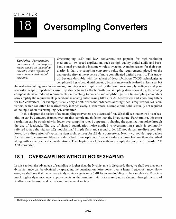
If is very active, can be approximated as an independent random num-ber uniformly distributed between , where equals the difference betweentwo adjacent quantization levels. Thus, the quantization noise power equals
(from Section 15.3) and is independent of t he sam pling frequency, .Also, the spectral density of , , is white (i.e., a constant over frequency)and all its power is within (a two-sided definition of power).
Assuming white quantization noise, the spectral density of the quantiza-tion noise, appears as shown in Fig. 18.2.
e n( )
Fig. 18.1 Quantizer and its linear model.
x n( ) y n( )y n( )x n( )
e n( )
Quantizer Model
e n( ) y n( ) x n( )–=
y n( ) x n( )
x n( )e n( ) e n( )
ΔΣ
Key Point: Quantization with a step size “LSB” can be mod-eled as an additive quantization noise uniformly distributed between –LSB/2 and +LSB/2 with a white power spectrum and total power of LSB2/12.
x n( ) e n( )Δ 2⁄± Δ
Δ2 12⁄ fs
e n( ) Se f( )f± s 2⁄
Se f( )
Fig. 18.2 Assumed spectral density of quantization noise.
0 fs
2---
Se f( )
ffs
2---–
kxΔ
12----------⎝ ⎠⎛ ⎞ 1
fs
---=Height
c18.fm Page 697 Sunday, October 23, 2011 3:31 PM
698 Chapter 18 • Oversampling Converters
The spectral density height is calculated by noting that the total noise power is and, with a two-sideddefinition of power, equals the area under within , or mathematically,
(18.1)
Solving this relation gives
(18.2)
EXAMPLE 18.1
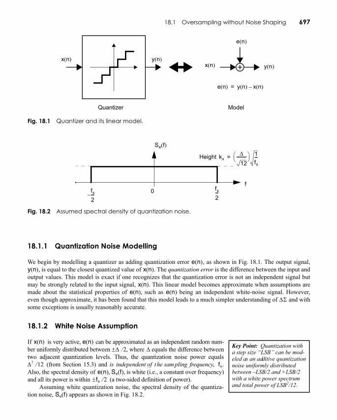
Find the output and quantization errors for two different quantizers, as shown in Fig. 18.3, when the inputvalues are
(18.3)
Also find the expected power and the power density height, , of the quantization noise when the samplingfrequency is normalized to .
SolutionThe output and quantization noise values for this example are given in Table 18.1. Note that although the outputsignals, , are well-defined values, the quantization error values can be approximated as uniformly distributedrandom numbers since the input signal is quite active.
Recalling that the quantization noise power is given by
(18.4)
then the expected noise powers of the two quantizers are
(18.5)
Δ2 12⁄Se f( ) f± s 2⁄
Se2 f( ) df
fs 2⁄–
fs 2⁄
∫ kx2 df
fs 2⁄–
fs 2⁄
∫ kx2fs
Δ2
12------= = =
kxΔ
12----------⎝ ⎠⎜ ⎟⎛ ⎞ 1
fs
---=
Fig. 18.3 Two example quantizers.
0.25 0.75
0.5–
1.0–
1.0
0.5
0.25–0.75–
y n( )
x n( )
Quantizer I(Five-level quantizer)
x n( )
y n( )
Quantizer II(Two-level quantizer)
1.0–
1.0
Δ 0.5= Δ 2.0=
x n( ) 0.01 0.31 0.11– 0.80 0.52 0.70–, , , , ,{ }=
Se2 f( )
2π rad sample⁄
y n( )
PeΔ12------
2=
PI0.52
12--------- 0.0208 W= =
c18.fm Page 698 Sunday, October 23, 2011 3:31 PM
18.1 Oversampling without Noise Shaping 699
(18.6)
where we note that these values are not affected by normalizing the sampling frequency. Also note that the twopower estimates for and correspond to rms power levels of and , respectively.
For the power density, we note that the power is spread evenly between , resulting in a density of
(18.7)
which results in
(18.8)
(18.9)
18.1.3 Oversampling Advantage
Oversampling occurs when the signals of interest are bandlimited to yet the sample rate is at , where ( being the Nyquist rate or, equivalently, the minimum sampling rate for signals bandlimited to ). We definethe oversampling ratio, OSR, as
(18.10)
After quantization, since the signals of interest are all below , is filtered by to create the signal, as shown in Fig. 18.4. This filter eliminates quantization noise (together with any other signals) greater
than . Assuming the input signal is a sinusoidal wave, its maximum peak value without clipping is . For
this maximum sinusoidal wave, the signal power, , has a power equal to
(18.11)
Table 18.1 Example signal values and quantizationnoise for two quantizers.
x(n)
Quantizer I(Five Levels)
Quantizer II(Two Levels)
y(n) e(n) y(n) e(n)
0.01 0.0 –0.01 1 0.990.31 0.5 0.19 1 0.69
–0.11 0.0 0.11 –1 –0.890.80 1.0 0.2 1 0.200.52 0.5 –0.02 1 0.48
–0.70 –0.5 0.2 –1 –0.30
PII22
12------ 0.333 W= =
PI PII 0.144 0.577fs 2⁄±
Se2 f( ) Pe
fs
------=
SeI2 f( ) 0.0208
2π----------------⎝ ⎠⎛ ⎞ 0.00331 W
rad sample⁄----------------------------= =
SeII2 f( ) 0.333
2π-------------⎝ ⎠⎛ ⎞ 0.053 W
rad sample⁄----------------------------= =
f0 fs fs 2f0>2f0 f0
OSRfs
2f0
------≡
f0 y1 n( ) H f( )y2 n( )
f0
2N Δ 2⁄( )Ps
PsΔ2N
2 2----------⎝ ⎠⎜ ⎟⎛ ⎞ 2
Δ222N
8-------------= =
c18.fm Page 699 Sunday, October 23, 2011 3:31 PM
700 Chapter 18 • Oversampling Converters
The power of the input signal within remains the same as before since we assumed the signal’s fre-quency content is below . However, the quantization noise power is reduced to
(18.12)
Therefore, doubling OSR (i.e., sampling at twice the rate) decreases the quantization noise power by one-halfor, equivalently, 3 dB (or, equivalently, 0.5 bits).
We can also calculate the maximum SQNR (in ) to be the ratio of the maximum sinusoidal power to thequantization noise power in the signal . Mathematically, we have through the use of (18.11) and (18.12)
(18.13)
which is also equal to
(18.14)
The first term is the SQNR due to the N-bit quantizer while the OSR term is theSQNR enhancement obtained from oversampling. Here we see that straightoversampling gives a SQNR improvement of or, equivalently,
. The reason for this SQNR improvement through the use ofoversampling is that when quantized samples are averaged together, the signalportion adds linearly, whereas the noise portion adds as the square root of thesum of the squares. Note that this enhancement also takes place with respect toother types of noise, such as thermal noise in circuits. Hence, oversampling
generally improves overall signal to noise ratio (SNR) by 10 log(OSR).
Fig. 18.4 (a) A possible oversampling system without noise shaping. (b) The brick-wall response of the filter to remove much of the quantization noise.
N-bit quantizer
u n( ) y2 n( )y1 n( )
H f( )
0 f0 fs
2---
ff0–fs
2---–
H f( )
1
(a)
(b)
y2 n( )f0
Pe Se2 f( ) H f( ) 2 df
fs 2⁄–
fs 2⁄
∫ kx2 df
f0–
f0∫2f0
fs
------Δ2
12------ Δ2
12------ 1
OSR-------------⎝ ⎠⎛ ⎞= = = =
dBy2 n( )
SQNRmax 10 Ps
Pe
------⎝ ⎠⎛ ⎞log 10 3
2---22N
⎝ ⎠⎛ ⎞log 10 OSR( )log+= =
SQNRmax 6.02N 1.76 10 OSR( )log+ +=
Key Point: Oversampling a signal at OSR times the Nyquist rate, without spectrally shaping the quantization noise, results in a SNR enhancement of 10 log(OSR) dB.
3 dB/octave0.5 bits/octave
c18.fm Page 700 Sunday, October 23, 2011 3:31 PM
18.1 Oversampling without Noise Shaping 701
EXAMPLE 18.2
Consider a sampled dc signal, , of value 1 V where the measured voltage, , is plus a noise signal, .Assume is a random signal uniformly distributed between . What is the SNR for when looking atindividual values? If eight samples of are averaged together, roughly what is the new SNR? To illustrate theresults, use eight typical samples for of {0.94, –0.52, –0.73, 2.15, 1.91, 1.33, –0.31, 2.33}.
Solution
Referencing signals to , we calculate the power of and to both be 1 watt. Thus the SNR for is when looking at individual values. Note that it is difficult to see the signal value of in the example samples since the SNR is so poor.If eight samples are averaged, we are realizing a modest low-pass filter, resulting in the oversampling ratio
being approximately equal to 8 (this is a rough estimate since a brick-wall filter is not being used). Since eachoctave of oversampling results in a 3-dB SNR improvement, the averaged value should have a SNR of around
. Note that averaging the eight given samples results in , which more closely represents thesignal value of .
The reason oversampling improves the SNR here is that by summing eight measured values, the eight signalvalues add linearly to 8 (or 64 watts) while the eight noise values add to (or 8 watts), since the noisevalues are assumed to be independent.
EXAMPLE 18.3
Given that a 1-bit A/D converter has a 6-dB SQNR, what sample rate is required using oversampling (no noiseshaping) to obtain a 96-dB SQNR (i.e., 16 bits) if ? (Note that the input into the A/D converter hasto be very active for the white-noise quantization model to be valid—a difficult arrangement when using a 1-bit quantizer with oversampling without noise shaping.)
Solution
Oversampling (without noise shaping) gives where 1 octave implies doubling the sampling rate. Werequire divided by , or 30 octaves. Thus, the required sampling rate, , is
!
This example shows why noise shaping is needed to improve the SQNR faster than , since is highly impractical.
18.1.4 The Advantage of 1-Bit D/A Converters
While oversampling improves the signal-to-noise ratio, it does not improve linearity. For example, if a 16-bitlinear converter is desired while using a 12-bit converter with oversampling, the 12-bit converter must have anintegral nonlinearity error less than LSB (here, LSB refers to that for a 12-bit converter). In other words,the component accuracy would have to match better than 16-bit accuracy (i.e., percent
Vs Vmeas Vs Vnoise
Vnoise 3± Vmeas
Vmeas
Vmeas
1 Ω Vs Vnoise Vmeas
0 dB Vmeas 1 VVmeas
9 dB Vmeas 0.88751 V
Vrms 8 Vrms
f0 25 kHz=
3 dB octave⁄90 dB 3 dB octave⁄ fs
fs 230 2f0× 54,000 GHz≅=
3 dB/octave54,000 GHz
1 24⁄100 × 1 216⁄( ) 0.0015=
c18.fm Page 701 Sunday, October 23, 2011 3:31 PM
702 Chapter 18 • Oversampling Converters
accuracy). Thus, some sort of auto calibration or laser trimming must be used toobtain the required linearity. However, as we saw in Example 18.3, with a highenough sampling rate, the output from a 1-bit converter can be filtered to obtainthe equivalent of a 16-bit converter. The advantage of a 1-bit D /A is that it isinherently linear.2 This linearity is a result of a 1-bit D/A converter having onlytwo output values and, since two points define a straight line, no trimming orcalibration is required. This inherent linearity is one of the major motivations formaking use of oversampling techniques with 1-bit converters. In fact, the reader
may be aware that many audio converters use 1-bit converters for realizing 16- to 18-bit linear converters (withnoise shaping). In fact, 20-bit linearity has been reported without the need for any trimming [Leopold, 1991].Finally, it should be mentioned that there are other advantages when using oversampling techniques, such as areduced requirement for analog anti-aliasing and smoothing filters.
18.2 OVERSAMPLING WITH NOISE SHAPINGIn this section, the advantage of noise shaping the quantization noise through the use of feedback is discussed.Here, we shall see a much more dramatic improvement in dynamic range when the input signal is oversampled ascompared to oversampling the input signal with no noise shaping. Although this section illustrates the basic prin-ciples with reference to A/D converters, much of it applies directly to D/A converters as well.
The system architecture of a oversampling A/D converter is shown in Fig. 18.5. The first stage is a con-tinuous-time anti-aliasing filter and is required to band-limit the input signal to frequencies less than one-half theoversampling frequency, . When the oversampling ratio is large, the anti-aliasing filter can often be quite simple,such as a simple RC low-pass filter. Following the anti-aliasing filter, the continuous-time signal, , is sampledby a sample and hold. This signal is then processed by the modulator, which converts the analog signal into anoise-shaped low-resolution digital signal. The third block in the system is a decimator. It converts the oversam-pled low-resolution digital signal into a high-resolution digital signal at a lower sampling rate usually equal totwice the frequency of the desired bandwidth of the input signal. The decimation filter can be conceptuallythought of as a low-pass filter followed by a down sampler, although in many systems the decimation is per-formed in a number of stages. It should be mentioned that in many realizations where the modulator is real-ized using switched-capacitor circuitry, a separate sample-and-hold is not required, as the continuous-time signal
2. This assumes that second-order errors due to imperfections such as signal-dependent power supply, or reference voltages, or memory in the D/A converter are not present.
Key Point: One-bit D/A con-verters are inherently linear. Hence, when combined with a high oversampling ratio, they can provide a good signal to quantization noise and dis-tortion ratio.
ΔΣΔΣ
Fig. 18.5 Block diagram of an oversampling A/D converter.
Sampleand
Digital
filterholdlow-passmod
ΔΣ
xsh t( ) xlp n( ) xs n( )xc t( )
fs fs fs 2f0
xdsm n( )
OSRAnti-
aliasingfilter
xin t( )
AnalogDigital
Decimation filter
fs
xc t( )ΔΣ
ΔΣ
c18.fm Page 702 Sunday, October 23, 2011 3:31 PM
18.2 Oversampling with Noise Shaping 703
is inherently sampled by the switches and input capacitors of the SC . In the next few sections the operation ofthe various building blocks will be described in greater detail.
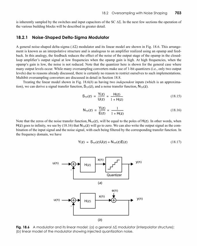
18.2.1 Noise-Shaped Delta-Sigma Modulator
A general noise-shaped delta-sigma ( ) modulator and its linear model are shown in Fig. 18.6. This arrange-ment is known as an interpolative structure and is analogous to an amplifier realized using an opamp and feed-back. In this analogy, the feedback reduces the effect of the noise of the output stage of the opamp in the closed-loop amplifier’s output signal at low frequencies when the opamp gain is high. At high frequencies, when theopamp’s gain is low, the noise is not reduced. Note that the quantizer here is shown for the general case wheremany output levels occur. While many oversampling converters make use of 1-bit quantizers (i.e., only two outputlevels) due to reasons already discussed, there is certainly no reason to restrict ourselves to such implementations.Multibit oversampling converters are discussed in detail in Section 18.8.
Treating the linear model shown in Fig. 18.6(b) as having two independent inputs (which is an approxima-tion), we can derive a signal transfer function, , and a noise transfer function, .
(18.15)
(18.16)
Note that the zeros of the noise transfer function, , will be equal to the poles of . In other words, when goes to infinity, we see by (18.16) that will go to zero. We can also write the output signal as the com-
bination of the input signal and the noise signal, with each being filtered by the corresponding transfer function. Inthe frequency domain, we have
(18.17)
ΔΣ
ΔΣ
Fig. 18.6 A modulator and its linear model: (a) a general modulator (interpolator structure); (b) linear model of the modulator showing injected quantization noise.
ΔΣ
H z( )–
x n( )u n( ) y n( )
H z( )–
x n( )u n( ) y n( )
e n( )
Quantizer
(a)
(b)
STF z( ) NTF z( )
STF z( ) Y z( )U z( )-----------≡ H z( )
1 H z( )+--------------------=
NTF z( ) Y z( )E z( )-----------≡ 1
1 H z( )+--------------------=
NTF z( ) H z( )H z( ) NTF z( )
Y z( ) STF z( )U z( ) NTF z( )E z( )+=
c18.fm Page 703 Sunday, October 23, 2011 3:31 PM
704 Chapter 18 • Oversampling Converters
To noise-shape the quantization noise in a useful manner, we choose suchthat its magnitude is large from to (i.e., over the frequency band of interest).With such a choice, the signal transfer function, , will approximate unityover the frequency band of interest very similarly to an opamp in a unity-gainfeedback configuration. Furthermore, the noise transfer function, , willapproximate zero over the same band. Thus, the quantization noise is reducedover the frequency band of interest while the signal itself is largely unaffected.The high-frequency noise is not reduced by the feedback as there is little loop
gain at high frequencies. However, additional post filtering can remove the out-of-band quantization noise withlittle effect on the desired signal.
Before choosing specific functions for , note that the maximum level of the in-band input signal, ,must remain within the maximum levels of the feedback signal, ; otherwise the large gain in will causethe signal to saturate. For example, if a quantizer having output levels of is used, the input signalmust also remain within for frequencies where the gain of is large. In fact, for many modulators theinput signal needs to be significantly smaller than the bounds of the quantizer output levels to keep the modula-tor stable.3 However, the maximum level of the input signal, , for frequencies where the gain of issmall will not necessarily cause the signal to saturate. In other words, the maximum level of the out-of-band input signal can be quite a bit larger than the feedback levels (see Problem 18.6).
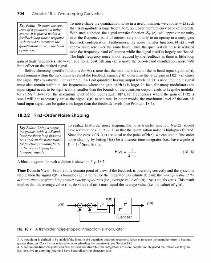
18.2.2 First-Order Noise Shaping
To realize first-order noise shaping, the noise transfer function, , shouldhave a zero at dc (i.e., ) so that the quantization noise is high-pass filtered.Since the zeros of are equal to the poles of , we can obtain first-ordernoise shaping by letting be a discrete-time integrator (i.e., have a pole at
).4 Specifically,
(18.18)
A block diagram for such a choice is shown in Fig. 18.7.
Time Domain View From a time domain point of view, if the feedback is operating correctly and the system isstable, then the signal is bounded (i.e., ). Since the integrator has infinite dc gain, the average value of thediscrete-time integrator’s input must exactly equal zero (i.e., average value of equals zero). This resultimplies that the average value (i.e., dc value) of must equal the average value (i.e., dc value) of .
3. A modulator is defined to be stable if the input to the quantizer does not become so large as to cause the quantizer error to become greater than (which is referred to as overloading the quantizer). See Section 18.7.4. A continuous-time integrator can also be used, but discrete-time integrators are more popular in integrated realizations as they are less sensitive to sampling jitter and have better distortion characteristics.
Key Point: To shape the spec-trum of a quantization noise source, it is placed within a feedback loop whose response is designed to attenuate the quantization noise in the band of interest.
H z( )0 f0
STF z( )
NTF z( )
H z( ) u n( )y n( ) H z( )
x n( ) 1-bit 1±1± H z( )
u n( ) H z( )
Δ 2⁄±
x n( )
Key Point: Using a single integrator inside a ΔΣ modu-lator feedback loop places a zero at dc in the noise trans-fer function providing first-order noise shaping for low-pass signals.
NTF z( )z 1=
NTF z( ) H z( )H z( )
z 1=
H z( ) 1z 1–------------=
Fig. 18.7 A first-order noise-shaped interpolative modulator.
–
x n( )u n( ) y n( )
Quantizer
z 1–
x n( ) ∞≠u n( ) y n( )–
u n( ) y n( )
c18.fm Page 704 Sunday, October 23, 2011 3:31 PM

18.2 Oversampling with Noise Shaping 705
Again, the similarity of this configuration and an opamp having unity-gain feedback is emphasized. Theopen-loop transfer function of an opamp is closely approximated by a first-order integrator having very large gainat low frequencies.
EXAMPLE 18.4
Find the output sequence and state values for a dc input, , of when a two-level quantizer of is used(threshold at zero) and the initial state for is 0.1.
SolutionThe output sequence and state values are given in Table 18.2.
Note that the average of exactly equals as expected. However, also note that the output pattern isperiodic, which implies that the quantization noise is not random in this example. (However, the result is muchmore satisfying than applying directly into a 1-bit quantizer using straight oversampling, which would giveall 1s as its output.)
Frequency Domain View From a frequency domain view, the signal transfer function, , is given by
(18.19)
and the noise transfer function, , is given by
(18.20)
We see here that the signal transfer function is simply a delay, while the noise transfer function is a discrete-timedifferentiator (i.e., a high-pass filter).
To find the magnitude of the noise transfer function, , we let and write the following:
(18.21)
u n( ) 1 3⁄ 1.0±x n( )
y n( ) 1 3⁄
1 3⁄
STF z( )
STF z( ) Y z( )U z( )----------- 1 z 1–( )⁄
1 1 z 1–( )⁄+--------------------------------- z 1–= = =
NTF z( )
NTF z( ) Y z( )E z( )----------- 1
1 1 z 1–( )⁄+--------------------------------- 1 z 1––( )= = =
NTF f( ) z = ejωT ej2πf fs⁄=
NTF f( ) 1 ej– 2πf fs⁄–
ejπf fs⁄ e
jπf– fs⁄–
2j--------------------------------- 2j e
jπ f– fs⁄××= =
πffs
-----⎝ ⎠⎛ ⎞sin 2j e
jπf– fs⁄××=
Table 18.2 First-order modulator example.
n x(n) x(n + 1) y(n) e(n)0 –0.1000 –0.5667 –1.0 –0.90001 –0.5667 –0.7667 –1.0 –0.43332 –0.7667 –0.1000 –1.0 –0.23333 –0.1000 –0.5667 –1.0 –0.90004 –0.5667 –0.7667 –1.0 –0.43335 . . . . . . . . . . . .
c18.fm Page 705 Sunday, October 23, 2011 3:31 PM
706 Chapter 18 • Oversampling Converters
Taking the magnitude of both sides, we have the high-pass function
(18.22)
Now the quantization noise power over the frequency band from to is given by
(18.23)
and making the approximation that (i.e., ), so that we can approximate to be, we have
(18.24)
Assuming the maximum signal power is the same as that obtained before in (18.11), the maximum SNR for thiscase is given by
(18.25)
or, equivalently,
(18.26)
We see here that doubling the OSR gives an SQNR improvement for a first-ordermodulator of or, equivalently, a gain of 1.5 bits/octave. This result should becompared to the 0.5 bits/octave when oversampling with no noise shaping.
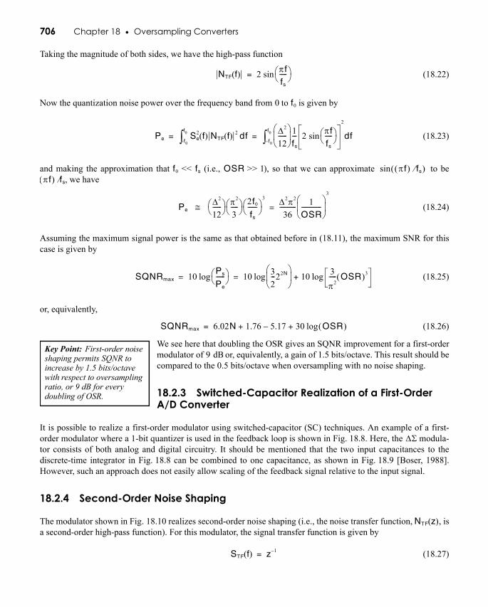
18.2.3 Switched-Capacitor Realization of a First-Order A/D Converter
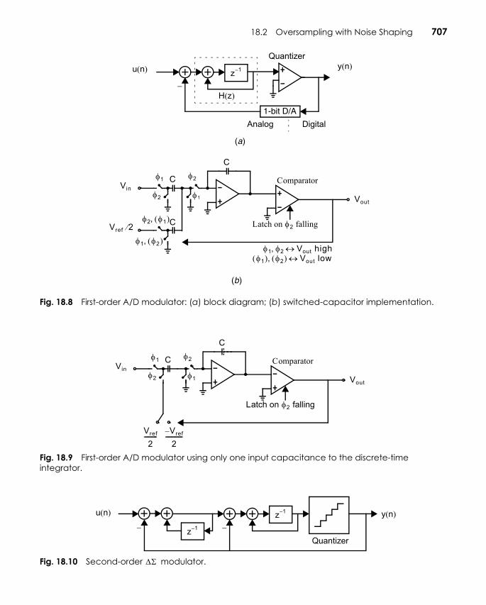
It is possible to realize a first-order modulator using switched-capacitor (SC) techniques. An example of a first-order modulator where a 1-bit quantizer is used in the feedback loop is shown in Fig. 18.8. Here, the modula-tor consists of both analog and digital circuitry. It should be mentioned that the two input capacitances to thediscrete-time integrator in Fig. 18.8 can be combined to one capacitance, as shown in Fig. 18.9 [Boser, 1988].However, such an approach does not easily allow scaling of the feedback signal relative to the input signal.
18.2.4 Second-Order Noise Shaping
The modulator shown in Fig. 18.10 realizes second-order noise shaping (i.e., the noise transfer function, , isa second-order high-pass function). For this modulator, the signal transfer function is given by
(18.27)
NTF f( ) 2 πffs
-----⎝ ⎠⎛ ⎞sin=
0 f0
Pe Se2 f( ) NTF f( ) 2 df
f0–
f0∫Δ2
12------⎝ ⎠⎜ ⎟⎛ ⎞ 1
fs
--- 2 πffs
-----⎝ ⎠⎛ ⎞sin
2
dff0–
f0∫= =
f0 << fs OSR >> 1 πf( ) fs⁄( )sinπf( ) fs⁄
PeΔ2
12------⎝ ⎠⎛ ⎞ π2
3-----⎝ ⎠⎛ ⎞ 2f0
fs
------⎝ ⎠⎛ ⎞
3
≅ Δ2π2
36----------- 1
OSR-------------⎝ ⎠⎜ ⎟⎛ ⎞
3
=
SQNRmax 10 Ps
Pe
------⎝ ⎠⎛ ⎞log 10 3
2---22N
⎝ ⎠⎜ ⎟⎛ ⎞
log 10 3π2----- OSR( )3log+= =
SQNRmax 6.02N 1.76 5.17– 30 OSR( )log+ +=
Key Point: First-order noise shaping permits SQNR to increase by 1.5 bits/octave with respect to oversampling ratio, or 9 dB for every doubling of OSR.
9 dB
ΔΣ
NTF z( )
STF f( ) z 1–=
c18.fm Page 706 Sunday, October 23, 2011 3:31 PM
18.2 Oversampling with Noise Shaping 707
Fig. 18.8 First-order A/D modulator: (a) block diagram; (b) switched-capacitor implementation.
1-bit D/A
–
u n( ) y n( )Quantizer
z 1–
Analog Digital
H z( )
(a)
(b)
Vref 2⁄
Vin
Vout
C
C
C
φ2
φ2
φ1
φ1
φ2 φ1( ),
φ1 φ2( ),
Latch on φ2 falling
φ1 φ2, Vout high↔φ1( ) φ2( ), Vout low↔
Comparator
Fig. 18.9 First-order A/D modulator using only one input capacitance to the discrete-time integrator.
Vref
2---------
Vin
Vout
C
C φ2
φ2
φ1
φ1
Latch on φ2 falling
Comparator
V– ref
2------------
Fig. 18.10 Second-order modulator.ΔΣ
–
u n( ) y n( )
Quantizer
z 1–
– z 1–
c18.fm Page 707 Sunday, October 23, 2011 3:31 PM
708 Chapter 18 • Oversampling Converters
and the noise transfer function is given by
(18.28)
Additionally, the magnitude of the noise transfer function can be shown to be given by
(18.29)
resulting in the quantization noise power over the frequency band of interest being given by
(18.30)
Again, assuming the maximum signal power is that obtained in (18.11), the maximum SQNR for this case isgiven by
(18.31)
or, equivalently,
(18.32)
We see here that doubling the improves the SQNR for a second-ordermodulator by or, equivalently, a gain of 2.5 bits/octave.
The realization of the second-order modulator using switched-capacitor tech-niques is left as an exercise for the interested reader.
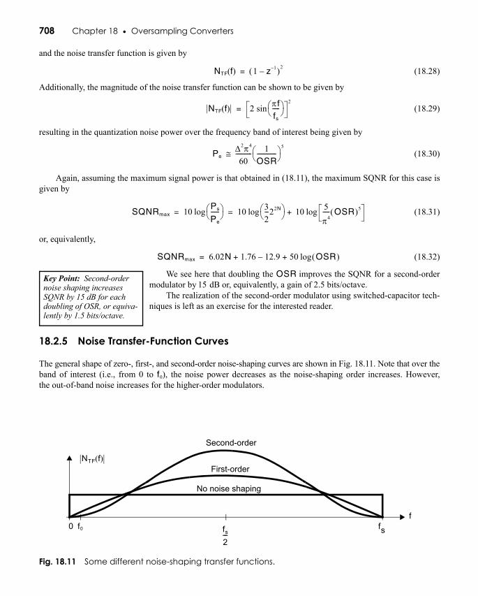
18.2.5 Noise Transfer-Function Curves
The general shape of zero-, first-, and second-order noise-shaping curves are shown in Fig. 18.11. Note that over theband of interest (i.e., from 0 to ), the noise power decreases as the noise-shaping order increases. However,the out-of-band noise increases for the higher-order modulators.
NTF f( ) 1 z 1––( )2=
NTF f( ) 2 πffs
-----⎝ ⎠⎛ ⎞sin
2=
PeΔ2π4
60----------- 1
OSR-------------⎝ ⎠⎛ ⎞ 5
≅
SQNRmax 10 Ps
Pe
------⎝ ⎠⎛ ⎞log 10 3
2---22N
⎝ ⎠⎛ ⎞log 10 5
π4----- OSR( )5log+= =
SQNRmax 6.02N 1.76 12.9– 50 OSR( )log+ +=
Key Point: Second-order noise shaping increases SQNR by 15 dB for each doubling of OSR, or equiva-lently by 1.5 bits/octave.
OSR15 dB
Fig. 18.11 Some different noise-shaping transfer functions.
0 f0 fsfs
2---
NTF f( )First-order
Second-order
No noise shaping
f
f0
c18.fm Page 708 Sunday, October 23, 2011 3:31 PM
18.2 Oversampling with Noise Shaping 709
EXAMPLE 18.5
Given that a 1-bit A/D converter has a -dB SQNR, what sample rate is required to obtain a -dB SNR (or16 bits) if kHz for straight oversampling as well as first- and second-order noise shaping?
Solution
Oversampling with No Noise Shaping From Example 18.3, straight oversampling requires a sampling rate of GHz.
First-Order Noise Shaping First-order noise shaping gives 9 dB/octave where 1 octave is doubling the OSR.Since we lose 5 dB, we require 95 dB divided by 9 dB/octave, or octaves. Thus, the required samplingrate, , is
MHz
This compares very favorably with straight oversampling, though it is still quite high.
Second-Order Noise Shaping Second-order noise shaping gives 15 dB/octave, but loses 13 dB. Thus werequired 103 dB divided by 15 dB/octave, resulting in a required sampling rate of only 5.8 MHz. However, thissimple calculation does not take into account the reduced input range for a second-order modulator needed for sta-bility.
18.2.6 Quantization Noise Power of 1-Bit Modulators
Assuming the output of a 1-bit modulator is , then one can immediately deter-mine the total power of the output signal, , to be a normalized power of 1 watt.Since consists of both signal and quantization noise, it is clear that the signalpower can never be greater than 1 watt. In fact, as alluded to earlier, the signallevel is often limited to well below the level in higher-order modulators tomaintain stability. For example, assuming that the maximum peak signal level isonly , then the maximum signal power is 62.5 mW (referenced to a load). This would imply a signal power approximately 12 dB less than is predicted by (18.11) and a correspond-ing reduction in the SQNR estimates that follow from (18.11). Since the signal power plus quantization noisepower equals 1 W, in this example the maximum signal power is about 12 dB below the total quantization noisepower. Fortunately, as we saw above, the quantization noise power is mostly in a different frequency region thanthe signal power and can therefore be filtered out. Note, however, that the filter must have a dynamic rangecapable of accommodating the full power of at its input. For a A/D converter, the filtering would bedone by digital filters following the quantizer.
18.2.7 Error-Feedback Structure
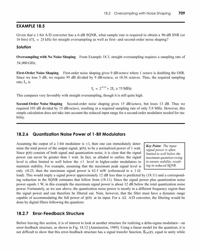
Before leaving this section, it is of interest to look at another structure for realizing a delta-sigma modulator—anerror-feedback structure, as shown in Fig. 18.12 [Anastassiou, 1989]. Using a linear model for the quantizer, it isnot difficult to show that this error-feedback structure has a signal transfer function, , equal to unity while
6 96f0 25=
54,000
10.56fs
fs 210.56 2f0× 75≅=
Key Point: The input signal power is often limited to well below the maximum quantizer swing to ensure stability, result-ing in reduced SQNR.
1±y n( )
y n( )
1±
0.25± 1 Ω
y n( ) ΔΣ
STF z( )
c18.fm Page 709 Sunday, October 23, 2011 3:31 PM
710 Chapter 18 • Oversampling Converters
the noise transfer function, , equals . Thus for a first-order modulator, , or in otherwords, the block is simply .
Unfortunately, a slight coefficient error can cause significant noise-shaping degradation with this error-feedback structure. For example, in a first-order case, if the delayed signal becomes (rather than ), then
, and the zero is moved off dc. Such a shift of the zero will result in the quantization noisenot being fully nulled at dc and therefore would not be suitable for high oversampling ratios. Thus, this structure is notwell suited to analog implementations where coefficient mismatch occurs. In contrast, an interpolative structure hasthe advantage that the zeros of the noise transfer function remain at dc as long as has infinite gain at dc. Thishigh gain at dc can usually be obtained in analog implementations by using opamps with large open-loop gains anddoes not rely on component matching. The error feedback structure is discussed here because it is useful for analysispurposes and can work well for fully digital implementations (such as in D/A converters) where no coefficientmismatches occur.
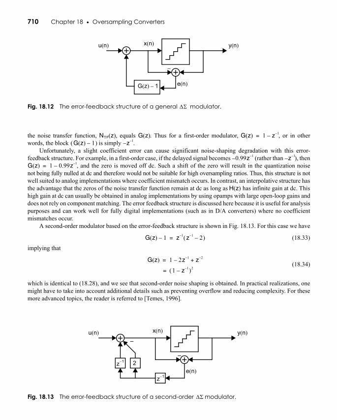
A second-order modulator based on the error-feedback structure is shown in Fig. 18.13. For this case we have
(18.33)
implying that
(18.34)
which is identical to (18.28), and we see that second-order noise shaping is obtained. In practical realizations, onemight have to take into account additional details such as preventing overflow and reducing complexity. For thesemore advanced topics, the reader is referred to [Temes, 1996].
Fig. 18.12 The error-feedback structure of a general modulator.
G z( ) 1–
y n( )
e n( )
x n( )u n( )
–
ΔΣ
NTF z( ) G z( ) G z( ) 1 z 1––=G z( ) 1–( ) z 1––
0.99z 1–– z 1––G z( ) 1 0.99z 1––=
H z( )
Fig. 18.13 The error-feedback structure of a second-order modulator.ΔΣ
y n( )
e n( )
x n( )u n( )
–z 1–
z 1–
2
–
G z( ) 1– z 1– z 1– 2–( )=
G z( ) 1 2z 1– z 2–+–=
1 z 1––( )2=
c18.fm Page 710 Sunday, October 23, 2011 3:31 PM
18.3 System Architectures 711
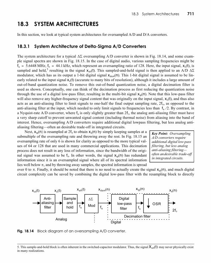
18.3 SYSTEM ARCHITECTURESIn this section, we look at typical system architectures for oversampled A/D and D/A converters.
18.3.1 System Architecture of Delta-Sigma A/D Converters
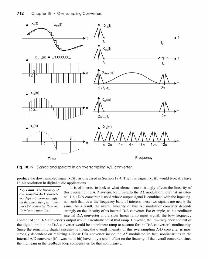
The system architecture for a typical oversampling A/D converter is shown in Fig. 18.14, and some exam-ple signal spectra are shown in Fig. 18.15. In the case of digital audio, various sampling frequencies might be
MHz, kHz, which represent an oversampling ratio of 128. Here, the input signal, , issampled and held,5 resulting in the signal . This sampled-and-held signal is then applied to an A/D modulator, which has as its output a 1-bit digital signal . This 1-bit digital signal is assumed to be lin-early related to the input signal (accurate to many bits of resolution), although it includes a large amount ofout-of-band quantization noise. To remove this out-of-band quantization noise, a digital decimation filter isused as shown. Conceptually, one can think of the decimation process as first reducing the quantization noisethrough the use of a digital low-pass filter, resulting in the multi-bit signal . Note that this low-pass filterwill also remove any higher-frequency signal content that was originally on the input signal, , and thus alsoacts as an anti-aliasing filter to limit signals to one-half the final output sampling rate, , as opposed to theanti-aliasing filter at the input, which needed to only limit signals to frequencies less than . By contrast, ina Nyquist-rate A/D converter, where is only slightly greater than , the analog anti-aliasing filter must havea very sharp cutoff to prevent unwanted signal content (including thermal noise) from aliasing into the band ofinterest. Hence, oversampling A/D converters require additional digital lowpass filtering, but less analog anti-aliasing filtering—often an desirable trade-off in integrated circuits.
Next, is resampled at to obtain by simply keeping samples at asubmultiple of the oversampling rate and throwing away the rest. In Fig. 18.15 anoversampling rate of only 6 is shown for clarity as opposed to the more typical val-ues of 64 or 128 that are used in many commercial applications. This decimationprocess does not result in any loss of information, since the bandwidth of the origi-nal signal was assumed to be . In other words, the signal has redundantinformation since it is an oversampled signal where all of its spectral informationlies well below , and by throwing away samples, the spectral information is spreadover 0 to . Finally, it should be noted that there is no need to actually create the signal , and much digitalcircuit complexity can be saved by combining the digital low-pass filter with the resampling block to directly
5. This sample-and-hold block is often inherent in the switched-capacitor modulator. Thus, the signal may never physically exist in many realizations.
ΔΣ
Fig. 18.14 Block diagram of an oversampling A/D converter.
Sampleand
Digital
filterholdlow-passMod
ΔΣ
xsh t( ) xlp n( ) xs n( )xc t( )
fs fs fs 2f0
xdsm n( )
OSRAnti-
aliasingfilter
xin t( )
AnalogDigital
Decimation filter
fs 5.6448= f0 44.1= xc t( )xsh t( ) ΔΣ
Xsh t( )
xdsm n( )xc t( )
xlp n( )xc t( )
2f0
fs 2⁄fs 2f0
Key Point: Oversampling A/D converters require additional digital low-pass filtering, but less analog anti-aliasing filtering—often an desirable trade-off in integrated circuits.
xlp n( ) 2f0 xs n( )
f0 xlp n( )
ππ xlp n( )
c18.fm Page 711 Sunday, October 23, 2011 3:31 PM
712 Chapter 18 • Oversampling Converters
produce the downsampled signal , as discussed in Section 18.4. The final signal, , would typically have resolution in digital audio applications.
It is of interest to look at what element most strongly affects the linearity ofthis oversampling A/D system. Returning to the modulator, note that an inter-nal 1-bit D/A converter is used whose output signal is combined with the input sig-nal such that, over the frequency band of interest, these two signals are nearly thesame. As a result, the overall linearity of this modulator converter dependsstrongly on the linearity of its internal D/A converter. For example, with a nonlinearinternal D/A converter and a slow linear ramp input signal, the low-frequency
content of the D/A converter’s output would essentially equal that ramp. However, the low-frequency content ofthe digital input to the D/A converter would be a nonlinear ramp to account for the D/A converter’s nonlinearity.Since the remaining digital circuitry is linear, the overall linearity of this oversampling A/D converter is moststrongly dependent on realizing a linear D/A converter inside the modulator. In fact, nonlinearities in theinternal A/D converter (if it was multi-bit) have only a small effect on the linearity of the overall converter, sincethe high gain in the feedback loop compensates for that nonlinearity.
Fig. 18.15 Signals and spectra in an oversampling A/D converter.
Time Frequency
xc t( )
t f
Xc f( )xsh t( )
f
Xsh f( )
fsf0
n
xdsm n( ) 1.000000±=
fsf0
xlp n( )
n
ω
ω
Xlp ω( )
Xdsm ω( )
2π
xs n( )
n ω
Xs ω( )
2πf0 fs⁄
2π2πf0 fs⁄
2ππ 4π 6π 8π 10π 12π1 23
123 …
…
123
4 …
…
xs n( ) xs n( )16-bit
Key Point: The linearity of oversampled A/D convert-ers depends more strongly on the linearity of its inter-nal D/A converter than on its internal quantizer.
ΔΣ
ΔΣ
ΔΣ
c18.fm Page 712 Sunday, October 23, 2011 3:31 PM
18.3 System Architectures 713
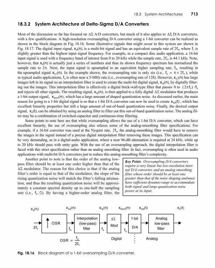
18.3.2 System Architecture of Delta-Sigma D/A Converters
Most of the discussion so far has focused on A/D converters, but much of it also applies to D/A converters,with a few qualifications. A high-resolution oversampling D/A converter using a 1-bit converter can be realized asshown in the block diagram in Fig. 18.16. Some illustrative signals that might occur in this system are shown inFig. 18.17. The digital input signal, , is a multi-bit signal and has an equivalent sample rate of , where isslightly greater than the highest input signal frequency. For example, in a compact disc audio application, a 16-bitinput signal is used with a frequency band of interest from 0 to 20 kHz while the sample rate, , is 44.1 kHz. Note,however, that is actually just a series of numbers and thus its shown frequency spectrum has normalized thesample rate to . Next, the input signal is upsampled to an equivalent higher sampling rate, , resulting inthe upsampled signal . In the example shown, the oversampling rate is only six (i.e., ), whilein typical audio applications, is often near a 5-MHz rate (i.e., oversampling rate of 128). However, has largeimages left in its signal so an interpolation filter is used to create the multi-bit digital signal, , by digitally filter-ing out the images. This interpolation filter is effectively a digital brick-wall-type filter that passes to and rejects all other signals. The resulting signal, , is then applied to a fully digital modulator that producesa 1-bit output signal, , which has a large amount of shaped quantization noise. As discussed earlier, the mainreason for going to a 1-bit digital signal is so that a 1-bit D/A converter can now be used to create , which hasexcellent linearity properties but still a large amount of out-of-band quantization noise. Finally, the desired outputsignal, , can be obtained by using an analog filter to filter out this out-of-band quantization noise. The analog fil-ter may be a combination of switched-capacitor and continuous-time filtering.
Some points to note here are that while oversampling allows the use of a 1-bit D/A converter, which can haveexcellent linearity, the use of oversampling also relaxes some of the analog-smoothing filter specifications. Forexample, if a 16-bit converter was used at the Nyquist rate, , the analog-smoothing filter would have to removethe images in the signal instead of a precise digital interpolation filter removing these images. This specification canbe very demanding, as in a digital-audio application, where a near 96-dB attenuation is required at 24 kHz, while upto 20 kHz should pass with unity gain. With the use of an oversampling approach, the digital interpolation filter isfaced with this strict specification rather than an analog smoothing filter. In fact, oversampling is often used in audioapplications with multi-bit D/A converters just to reduce this analog-smoothing filter’s complexity.
Another point to note is that the order of the analog low-pass filter should be at least one order higher than that of the
modulator. The reason for this choice is that if the analogfilter’s order is equal to that of the modulator, the slope of therising quantization noise will match the filter’s falling attenua-tion, and thus the resulting quantization noise will be approxi-mately a constant spectral density up to one-half the samplingrate (i.e., ). By having a higher-order analog filter, the
ΔΣ ΔΣ
Fig. 18.16 Block diagram of a 1-bit oversampling D/A converter.
Interpolation
filter(low-pass) Mod
ΔΣ 1-bit
D/A
Analog
filterlow-pass
AnalogDigital
xs n( ) xs2 n( ) xlp n( ) xdsm n( ) xda t( ) xc t( )
2f0 fs fs fs
OSRfs
2f0
-------≡
OSR
xs n( ) 2f0 f0
2f0
xs n( )2π fs
xs2 n( ) fs 6 2f0×=fs xs2 n( )
xlp n( )0 2πf0( ) fs⁄
xlp n( ) ΔΣxdsm n( )
xda t( )
xc t( )
2f0
Key Point: Oversampling D/A converters require a very linear but low-resolution inter-nal D/A converter, and an analog smoothing filter whose order should be at least one greater than that of the noise shaping and must have sufficient dynamic range to accommodate both signal and large quantization noise power at its input.
ΔΣ
fs 2⁄
c18.fm Page 713 Sunday, October 23, 2011 3:31 PM
714 Chapter 18 • Oversampling Converters
spectral density of the output signal’s quantization noise will have a bandwidth similar to the analog filter’sbandwidth, which is around .
Finally, note that the analog filter must be able to strongly attenuate high-frequency noise, as much of the quan-tization noise is centered around , and this analog filter should be linear so it does not modulate the noiseback to the frequency band of interest. In many applications, the realization of these filters, especially if they areintegrated, is nontrivial.
18.4 DIGITAL DECIMATION FILTERSThere are many techniques for realizing digital decimation filters in oversampling A/D converters. In this section, wediscuss two popular approaches—multi-stage and single-stage.
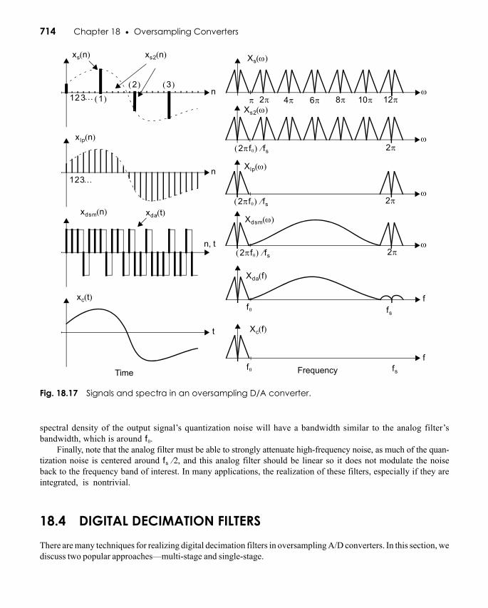
Fig. 18.17 Signals and spectra in an oversampling D/A converter.
xlp n( )
xdsm n( ) xda t( )
xc t( )
n
n
n t,
t
f
f
ω
ω
ω
ω
Xs ω( )
Xs2 ω( )
Xlp ω( )
Xdsm ω( )
Xda f( )
Xc f( )
Time Frequency
fs
fsf0
f0
xs n( ) xs2 n( )
2ππ 4π 6π 8π 10π 12π
2π2πf0( ) fs⁄
2π2πf0( ) fs⁄
2π2πf0( ) fs⁄
123
123 1( )
2( ) 3( )…
…
f0
fs 2⁄
c18.fm Page 714 Sunday, October 23, 2011 3:31 PM
18.4 Digital Decimation Filters 715
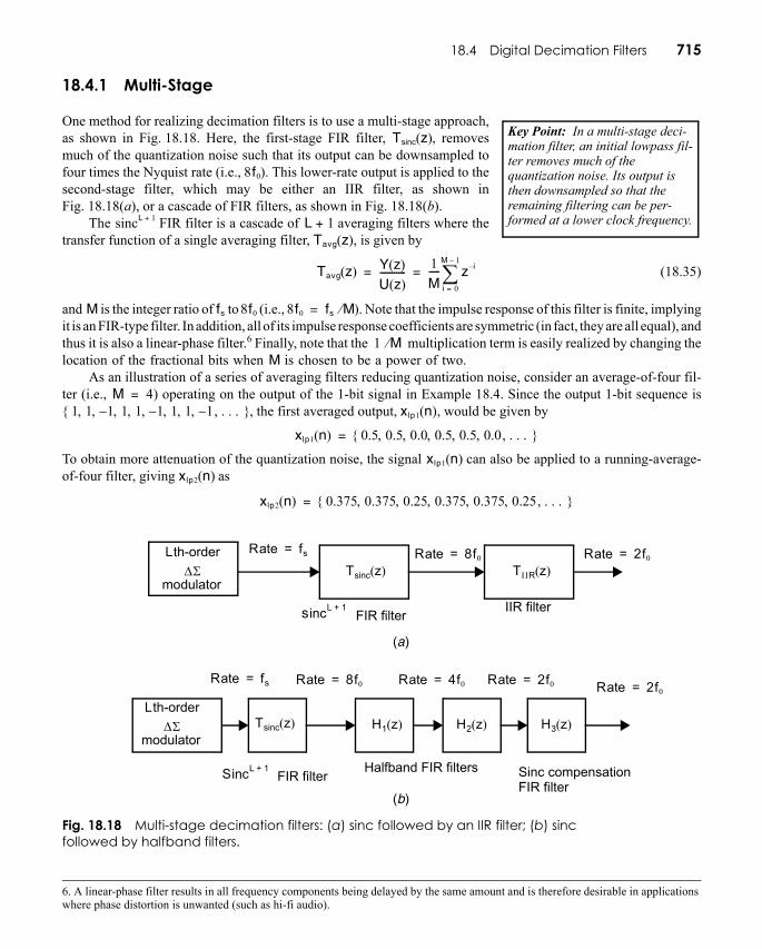
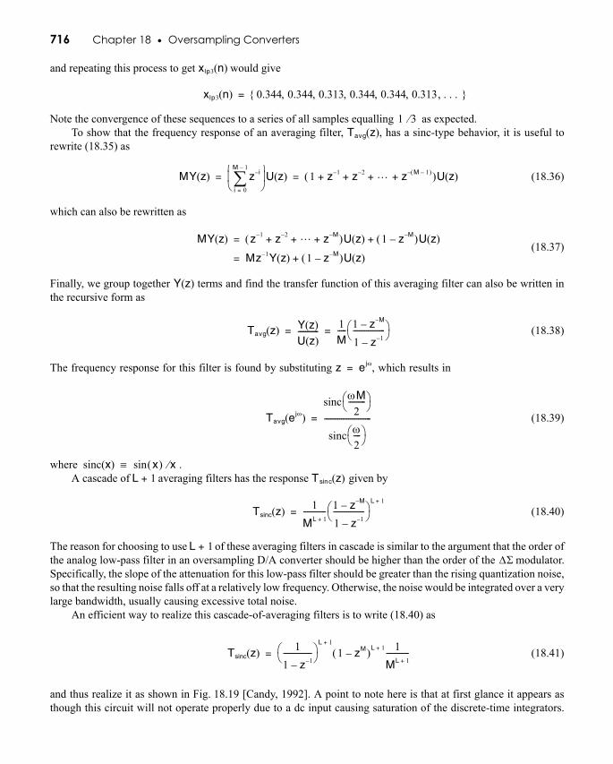
18.4.1 Multi-Stage
One method for realizing decimation filters is to use a multi-stage approach,as shown in Fig. 18.18. Here, the first-stage FIR filter, , removesmuch of the quantization noise such that its output can be downsampled tofour times the Nyquist rate (i.e., ). This lower-rate output is applied to thesecond-stage filter, which may be either an IIR filter, as shown inFig. 18.18(a), or a cascade of FIR filters, as shown in Fig. 18.18(b).
The FIR filter is a cascade of averaging filters where thetransfer function of a single averaging filter, , is given by
(18.35)
and is the integer ratio of to (i.e., ). Note that the impulse response of this filter is finite, implyingit is an FIR-type filter. In addition, all of its impulse response coefficients are symmetric (in fact, they are all equal), andthus it is also a linear-phase filter.6 Finally, note that the multiplication term is easily realized by changing thelocation of the fractional bits when is chosen to be a power of two.
As an illustration of a series of averaging filters reducing quantization noise, consider an average-of-four fil-ter (i.e., ) operating on the output of the 1-bit signal in Example 18.4. Since the output 1-bit sequence is
, the first averaged output, , would be given by
To obtain more attenuation of the quantization noise, the signal can also be applied to a running-average-of-four filter, giving as
6. A linear-phase filter results in all frequency components being delayed by the same amount and is therefore desirable in applications where phase distortion is unwanted (such as hi-fi audio).
Key Point: In a multi-stage deci-mation filter, an initial lowpass fil-ter removes much of the quantization noise. Its output is then downsampled so that the remaining filtering can be per-formed at a lower clock frequency.
Fig. 18.18 Multi-stage decimation filters: (a) sinc followed by an IIR filter; (b) sinc followed by halfband filters.
FIR filters incL 1+ IIR filter
Rate fs= Rate 8f0= Rate 2f0=ΔΣ
modulator
Lth-orderTsinc z( ) TIIR z( )
FIR filterSincL 1+ Halfband FIR filters
Rate fs= Rate 8f0= Rate 2f0=
ΔΣmodulator
Lth-orderTsinc z( )
Rate 4f0=
(a)
(b)
H1 z( ) H2 z( ) H3 z( )
Sinc compensationFIR filter
Rate 2f0=
Tsinc z( )
8f0
sincL 1+ L 1+Tavg z( )
Tavg z( ) Y z( )U z( )----------- 1
M----- z i–
i 0=
M 1–
∑= =
M fs 8f0 8f0 fs M⁄=
1 M⁄M
M 4=1 1 1– 1 1 1– 1 1 1, . . .–, , , , , , , ,{ } xlp1 n( )
xlp1 n( ) 0.5 0.5 0.0 0.5 0.5 0.0, . . ., , , , ,{ }=
xlp1 n( )xlp2 n( )
xlp2 n( ) 0.375 0.375 0.25 0.375 0.375 0.25, . . ., , , , ,{ }=
c18.fm Page 715 Sunday, October 23, 2011 3:31 PM
716 Chapter 18 • Oversampling Converters
and repeating this process to get would give
Note the convergence of these sequences to a series of all samples equalling as expected.To show that the frequency response of an averaging filter, , has a sinc-type behavior, it is useful to
rewrite (18.35) as
(18.36)
which can also be rewritten as
(18.37)
Finally, we group together terms and find the transfer function of this averaging filter can also be written inthe recursive form as
(18.38)
The frequency response for this filter is found by substituting , which results in
(18.39)
where . A cascade of averaging filters has the response given by
(18.40)
The reason for choosing to use of these averaging filters in cascade is similar to the argument that the order ofthe analog low-pass filter in an oversampling D/A converter should be higher than the order of the modulator.Specifically, the slope of the attenuation for this low-pass filter should be greater than the rising quantization noise,so that the resulting noise falls off at a relatively low frequency. Otherwise, the noise would be integrated over a verylarge bandwidth, usually causing excessive total noise.
An efficient way to realize this cascade-of-averaging filters is to write (18.40) as
(18.41)
and thus realize it as shown in Fig. 18.19 [Candy, 1992]. A point to note here is that at first glance it appears asthough this circuit will not operate properly due to a dc input causing saturation of the discrete-time integrators.
xlp3 n( )
xlp3 n( ) 0.344 0.344 0.313 0.344 0.344 0.313, . . ., , , , ,{ }=
1 3⁄Tavg z( )
MY z( ) z i–
i 0=
M 1–
∑⎝ ⎠⎜ ⎟⎛ ⎞
U z( ) 1 z 1– z 2– … z M 1–( )–+ + + +( )U z( )= =
MY z( ) z 1– z 2– … z M–+ + +( )U z( ) 1 z M––( )U z( )+=
Mz 1– Y z( ) 1 z M––( )U z( )+=
Y z( )
Tavg z( ) Y z( )U z( )----------- 1
M----- 1 z M––
1 z 1––-----------------⎝ ⎠⎛ ⎞= =
z ejω=
Tavg ejω( )sinc ωM
2---------⎝ ⎠⎛ ⎞
sinc ω2----⎝ ⎠⎛ ⎞
-------------------------=
sinc x( ) x( )sin x⁄≡L 1+ T csin z( )
Tsinc z( ) 1ML 1+------------ 1 z M––
1 z 1––-----------------⎝ ⎠⎛ ⎞
L 1+
=
L 1+ΔΣ
Tsinc z( ) 11 z 1––---------------⎝ ⎠⎛ ⎞
L 1+
1 zM–( )L 1+ 1ML 1+------------=
c18.fm Page 716 Sunday, October 23, 2011 3:31 PM
18.4 Digital Decimation Filters 717
Fortunately, such a result does not occur when 2’s-complement arithmetic is used due to its wrap-around charac-teristic. Specifically, although the dc levels at the integrator outputs may be incorrect, the differentiators comparethe present sample with that of samples past while rejecting the dc component. Thus, as long as this differenceis properly maintained (as it would be using 2’s-complement arithmetic) the correct calculation is performed.
Referring once again to Fig. 18.18, the purpose of the filters following the filter is twofold. One reasonfor their use is to remove any higher-frequency input signals (in effect, a sharp anti-aliasing filter) before the signalis downsampled to the final Nyquist rate (i.e., ). In other words, while the filter is good at filtering outthe quantization noise, it is not sharp enough to act as a reasonable anti-aliasing filter for input signals slightlyhigher than . A second reason is to compensate for the frequency drop in the passband caused by the filter.This anti-aliasing and sinc-compensation filter might be realized using a single IIR filter, as shown inFig. 18.18(a). Alternatively, a few halfband FIR filters might be used together with a separate sinc-compensationFIR filter, as shown in Fig. 18.18(b). A halfband FIR filter has a passband from 0 to , while its stopband isfrom to with every second coefficient being zero [Vaidyanathan, 1993]. Thus, with a high enough filterorder, its output can be downsampled by a factor of two. It has also been shown that in some applications, thesehalfband and sinc-compensation filters can be realized using no general multi-bit multipliers [Saramaki, 1990].
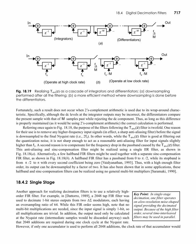
18.4.2 Single Stage
Another approach for realizing decimation filters is to use a relatively high-order FIR filter. For example, in [Dattorro, 1989], a 2048 tap FIR filter wasused to decimate 1-bit stereo outputs from two modulators, each havingan oversampling ratio of 64. While this FIR order seems high, note that nomulti-bit multiplications are needed, since the input signal is simply 1-bit, soall multiplications are trivial. In addition, the output need only be calculatedat the Nyquist rate (intermediate samples would be discarded anyway) suchthat 2048 additions are required during one clock cycle at the Nyquist rate.However, if only one accumulator is used to perform all 2048 additions, the clock rate of that accumulator would
Fig. 18.19 Realizing as a cascade of integrators and differentiators: (a) downsampling performed after all the filtering; (b) a more efficient method where downsampling is done before the differentiators.
Tsinc z( )
z 1– z 1– z M– z M– fs
M-----
OutIn
(a)
z 1– z 1– fs
M----- z 1– z 1–
(Operate at low clock rate)
OutIn
(Operate at high clock rate) (b)
(Integrators) (Differentiators)
––
– –
fs M⁄ fs M⁄fsfs
M
T csin z( )
2f0 T csin z( )
f0 T csin z( )
π 2⁄π 2⁄ π
Key Point: In single-stage decimation, one filter operates on a low-resolution noise-shaped signal providing the decimated output. Because of the high filter order, several time-interleaved filters may be used in parallel.
ΔΣ
c18.fm Page 717 Sunday, October 23, 2011 3:31 PM
718 Chapter 18 • Oversampling Converters
be 2048 times the Nyquist rate. For example, if the Nyquist rate is 48 kHz, the single accumulator would haveto be clocked at 98.3 MHz. To overcome this high clock rate, 32 separate FIR filters are realized (with sharedcoefficients) in a time-interleaved fashion, with each FIR having 2048 coefficients and each producing an outputat a clock rate of 1.5 kHz. In this way, each of the 32 FIR filters uses a single accumulator operating at 3 MHz(i.e., 2048 times 1.5 kHz). The coefficient ROM values were shared between the FIR filters (as well as in the twostereo channels), and the ROM size can also be halved if coefficients are duplicated, as in the case of linear-phaseFIR filtering.
Finally, it is also possible to reduce the number of additions by grouping together input bits. For example, iffour input bits are grouped together, then a 16-word ROM lookup table can be used rather than using three addi-tions. With such a grouping of input bits, each of the 32 FIR filters would require only 512 additions.
18.5 HIGHER-ORDER MODULATORSIn general, it can be shown that an Lth-order noise-shaping modulator improves theSQNR by dB/octave, or equivalently, bits/octave. In this section, welook at two approaches for realizing higher-order modulators—interpolative andMASH. The first approach is typically a single high-order structure with feedbackfrom the quantized signal. The second approach consists of a cascade of lower-order modulators, where the latter modulators are used to cancel the noise errorsintroduced by the earlier modulators.
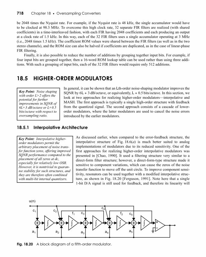
18.5.1 Interpolative Architecture
As discussed earlier, when compared to the error-feedback structure, theinterpolative structure of Fig. 18.6(a) is much better suited to analogimplementations of modulators due to its reduced sensitivity. One of thefirst approaches for realizing higher-order interpolative modulators waspresented in [Chao, 1990]. It used a filtering structure very similar to adirect-form filter structure; however, a direct-form-type structure made itsensitive to component variations, which can cause the zeros of the noisetransfer function to move off the unit circle. To improve component sensi-tivity, resonators can be used together with a modified interpolative struc-ture, as shown in Fig. 18.20 [Ferguson, 1991]. Note here that a single1-bit D/A signal is still used for feedback, and therefore its linearity will
Key Point: Noise shaping with order L>2 offers the potential for further improvements in SQNR of 6L+3 dB/octave or L+0.5 bits/octave with respect to oversampling ratio.
6L 3+ L 0.5+
Key Point: Interpolative higher-order modulators permit the arbitrary placement of noise trans-fer function zeros, offering improved SQNR performance compared to the placement of all zeros at dc, especially for relatively low OSR. However, it is nontrivial to guaran-tee stability for such structures, and they are therefore often combined with multi-bit internal quantizers.
Fig. 18.20 A block diagram of a fifth-order modulator.
∫ ∫ ∫ ∫ ∫
u n( )
a1 a2 a3 a4
c1 c2 c3f1 f2
c4
c5
a5
c18.fm Page 718 Sunday, October 23, 2011 3:31 PM
18.5 Higher-Order Modulators 719
be excellent. The resonators in this structure are due to the feedback signals associated with and , resulting inthe placement of zeros in the noise transfer function spread over the frequency-of-interest band. Such an arrange-ment gives better dynamic range performance than placing all the zeros at dc as we have been assuming thus far.
Unfortunately, it is possible for modulators of order two or more to go unstable, especially when largeinput signals are present. When they go unstable, they may never return to stability even when the large inputsignals go away. Guaranteeing stability for an interpolative modulator is nontrivial and is discussed further inSection 18.7. In particular, the use of multi-bit internal quantizers improves stability and is therefore often usedin combination with higher-order interpolative architectures.
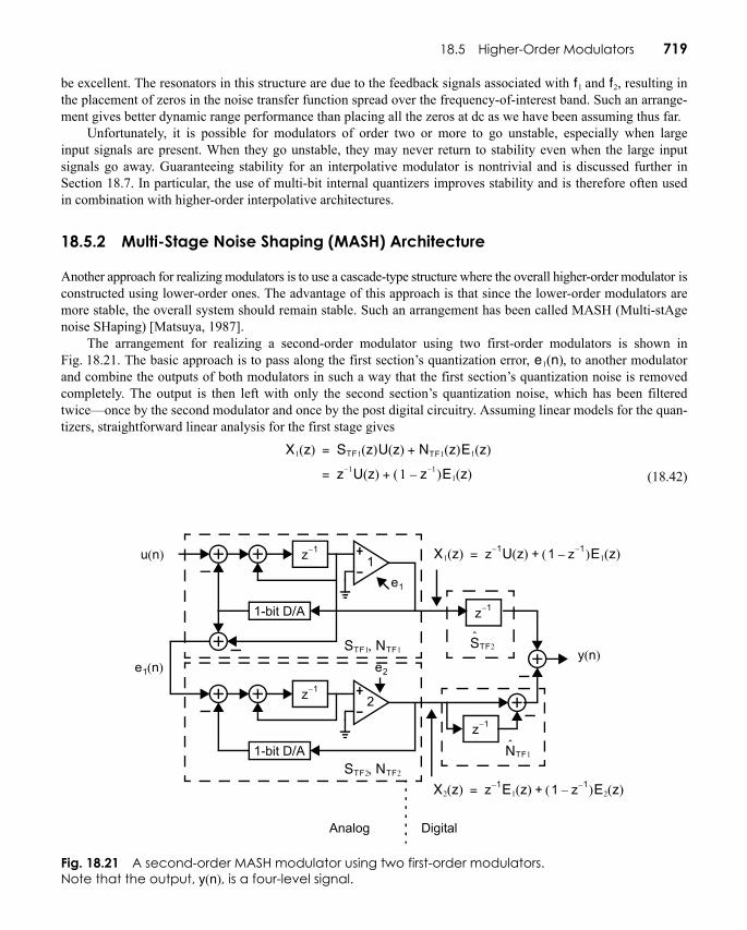
18.5.2 Multi-Stage Noise Shaping (MASH) Architecture
Another approach for realizing modulators is to use a cascade-type structure where the overall higher-order modulator isconstructed using lower-order ones. The advantage of this approach is that since the lower-order modulators aremore stable, the overall system should remain stable. Such an arrangement has been called MASH (Multi-stAgenoise SHaping) [Matsuya, 1987].
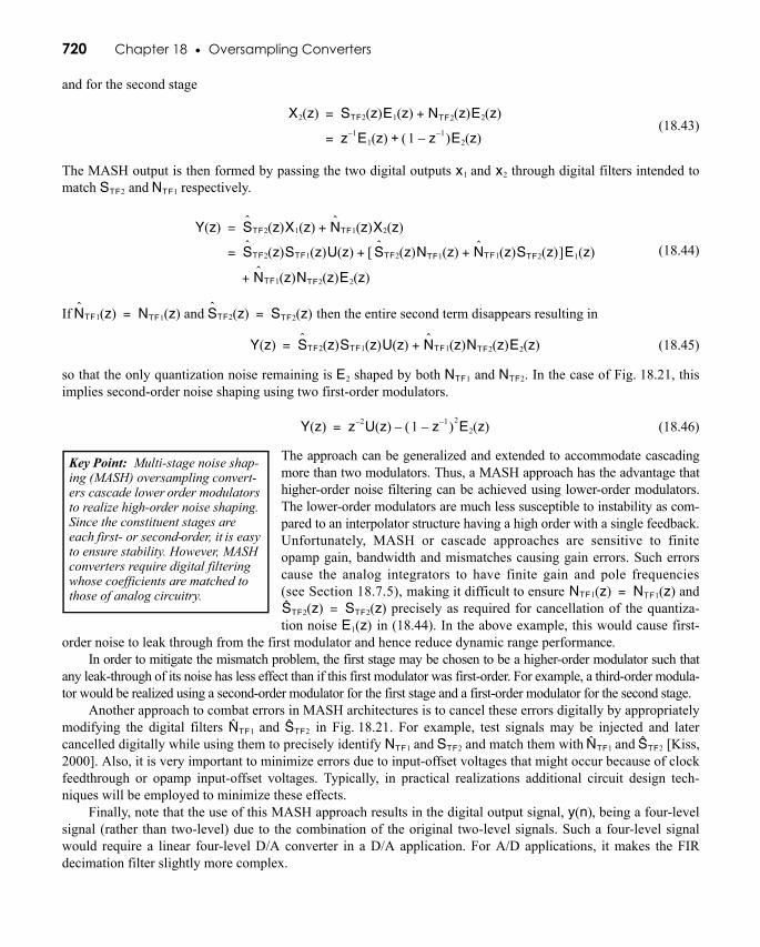
The arrangement for realizing a second-order modulator using two first-order modulators is shown inFig. 18.21. The basic approach is to pass along the first section’s quantization error, , to another modulatorand combine the outputs of both modulators in such a way that the first section’s quantization noise is removedcompletely. The output is then left with only the second section’s quantization noise, which has been filteredtwice—once by the second modulator and once by the post digital circuitry. Assuming linear models for the quan-tizers, straightforward linear analysis for the first stage gives
(18.42)
f1 f2
Fig. 18.21 A second-order MASH modulator using two first-order modulators. Note that the output, , is a four-level signal.y n( )
z 1–
1-bit D/A
z 1–
1-bit D/A
z 1–
z 1–
1
2
e1
e2
y n( )
u n( )
e1 n( )
X1 z( ) z 1– U z( ) 1 z 1––( )E1 z( )+=
X2 z( ) z 1– E1 z( ) 1 z 1––( )E2 z( )+=
STF2
NTF1
STF2 NTF2,
Analog Digital
STF1 NTF1,
e1 n( )
X1 z( ) STF1 z( )U z( ) N+ TF1 z( )E1 z( )=
z 1– U z( ) 1 z 1––( )E1 z( )+=
c18.fm Page 719 Sunday, October 23, 2011 3:31 PM
720 Chapter 18 • Oversampling Converters
and for the second stage
(18.43)
The MASH output is then formed by passing the two digital outputs and through digital filters intended tomatch and respectively.
(18.44)
If and then the entire second term disappears resulting in
(18.45)
so that the only quantization noise remaining is shaped by both and . In the case of Fig. 18.21, thisimplies second-order noise shaping using two first-order modulators.
(18.46)
The approach can be generalized and extended to accommodate cascadingmore than two modulators. Thus, a MASH approach has the advantage thathigher-order noise filtering can be achieved using lower-order modulators.The lower-order modulators are much less susceptible to instability as com-pared to an interpolator structure having a high order with a single feedback.Unfortunately, MASH or cascade approaches are sensitive to finiteopamp gain, bandwidth and mismatches causing gain errors. Such errorscause the analog integrators to have finite gain and pole frequencies(see Section 18.7.5), making it difficult to ensure and
precisely as required for cancellation of the quantiza-tion noise in (18.44). In the above example, this would cause first-
order noise to leak through from the first modulator and hence reduce dynamic range performance.In order to mitigate the mismatch problem, the first stage may be chosen to be a higher-order modulator such that
any leak-through of its noise has less effect than if this first modulator was first-order. For example, a third-order modula-tor would be realized using a second-order modulator for the first stage and a first-order modulator for the second stage.
Another approach to combat errors in MASH architectures is to cancel these errors digitally by appropriatelymodifying the digital filters and in Fig. 18.21. For example, test signals may be injected and latercancelled digitally while using them to precisely identify and and match them with and [Kiss,2000]. Also, it is very important to minimize errors due to input-offset voltages that might occur because of clockfeedthrough or opamp input-offset voltages. Typically, in practical realizations additional circuit design tech-niques will be employed to minimize these effects.
Finally, note that the use of this MASH approach results in the digital output signal, , being a four-levelsignal (rather than two-level) due to the combination of the original two-level signals. Such a four-level signalwould require a linear four-level D/A converter in a D/A application. For A/D applications, it makes the FIRdecimation filter slightly more complex.
X2 z( ) STF2 z( )E1 z( ) N+ TF2 z( )E2 z( )=
z 1– E1 z( ) 1 z 1––( )E2 z( )+=
x1 x2
STF2 NTF1
Y z( ) STF2 z( )X1 z( ) NTF1 z( )X2 z( )+=
STF2 z( )STF1 z( )U z( ) STF2 z( )NTF1 z( ) NTF1 z( )STF2 z( )+[ ]E1 z( )+=
NTF1 z( )NTF2 z( )E2 z( )+
NTF1 z( ) NTF1 z( )= STF2 z( ) STF2 z( )=
Y z( ) STF2 z( )STF1 z( )U z( ) NTF1 z( )NTF2 z( )E2 z( )+=
E2 NTF1 NTF2
Y z( ) z 2– U z( ) 1 z 1––( )2E2 z( )–=
Key Point: Multi-stage noise shap-ing (MASH) oversampling convert-ers cascade lower order modulators to realize high-order noise shaping. Since the constituent stages are each first- or second-order, it is easy to ensure stability. However, MASH converters require digital filtering whose coefficients are matched to those of analog circuitry. NTF1 z( ) NTF1 z( )=
STF2 z( ) STF2 z( )=E1 z( )
NTF1 STF2
NTF1 STF2 NTF1 STF2
y n( )
c18.fm Page 720 Sunday, October 23, 2011 3:31 PM
18.6 Bandpass Oversampling Converters 721
18.6 BANDPASS OVERSAMPLING CONVERTERSAs we have seen, oversampling converters have the advantage of high linearity through the use of 1-bit conversionand reduced anti-aliasing and smoothing-filter requirements. However, at first glance some signals do not appearto easily lend themselves to oversampling approaches such as modulated radio signals. Such signals have informa-tion in only a small amount of bandwidth, say 10 kHz, but have been modulated by some higher-frequency carriersignal, say 1 MHz. For such applications, one can make use of bandpass oversampling converters.
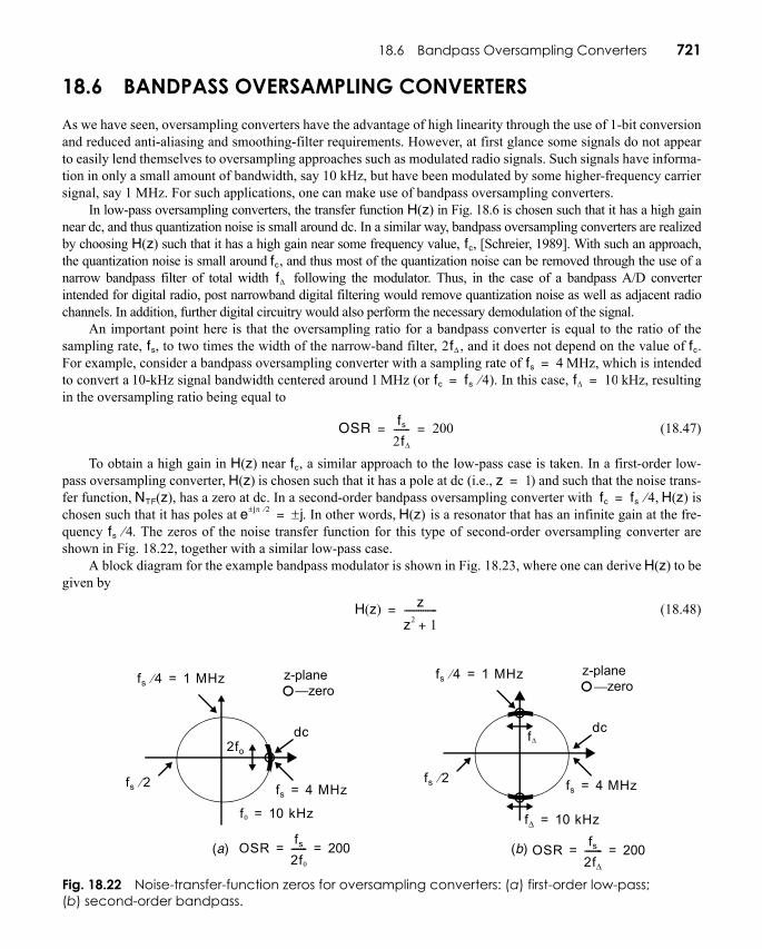
In low-pass oversampling converters, the transfer function in Fig. 18.6 is chosen such that it has a high gainnear dc, and thus quantization noise is small around dc. In a similar way, bandpass oversampling converters are realizedby choosing such that it has a high gain near some frequency value, , [Schreier, 1989]. With such an approach,the quantization noise is small around , and thus most of the quantization noise can be removed through the use of anarrow bandpass filter of total width following the modulator. Thus, in the case of a bandpass A/D converterintended for digital radio, post narrowband digital filtering would remove quantization noise as well as adjacent radiochannels. In addition, further digital circuitry would also perform the necessary demodulation of the signal.
An important point here is that the oversampling ratio for a bandpass converter is equal to the ratio of thesampling rate, , to two times the width of the narrow-band filter, , and it does not depend on the value of .For example, consider a bandpass oversampling converter with a sampling rate of MHz, which is intendedto convert a -kHz signal bandwidth centered around MHz (or ). In this case, kHz, resultingin the oversampling ratio being equal to
(18.47)
To obtain a high gain in near , a similar approach to the low-pass case is taken. In a first-order low-pass oversampling converter, is chosen such that it has a pole at dc (i.e., ) and such that the noise trans-fer function, , has a zero at dc. In a second-order bandpass oversampling converter with , ischosen such that it has poles at . In other words, is a resonator that has an infinite gain at the fre-quency . The zeros of the noise transfer function for this type of second-order oversampling converter areshown in Fig. 18.22, together with a similar low-pass case.
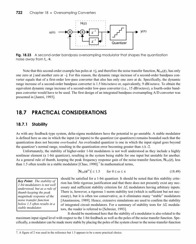
A block diagram for the example bandpass modulator is shown in Fig. 18.23, where one can derive to begiven by
(18.48)
H z( )
H z( ) fc
fc
fΔ
fs 2fΔ fc
fs 4=10 1 fc fs 4⁄= fΔ 10=
OSR fs
2fΔ------- 200= =
H z( ) fc
H z( ) z 1=NTF z( ) fc fs 4⁄= H z( )
e jπ 2⁄± j±= H z( )fs 4⁄
Fig. 18.22 Noise-transfer-function zeros for oversampling converters: (a) first-order low-pass;(b) second-order bandpass.
z-plane
(b)
fs 2⁄ fs 4 MHz=
dc
fs 4⁄ 1 MHz=—zero
fΔ 10 kHz=
z-plane
fs 4 MHz=
dc
fs 4⁄ 1 MHz=—zero
f0 10 kHz=
fs 2⁄
(a)
fΔ2fo
OSRfs
2f0
------- 200= = OSRfs
2fΔ-------- 200= =
H z( )
H z( ) z
z2 1+--------------=
c18.fm Page 721 Sunday, October 23, 2011 3:31 PM
722 Chapter 18 • Oversampling Converters
Note that this second-order example has poles at , and therefore the noise transfer function, , has onlyone zero at and another zero at . For this reason, the dynamic range increase of a second-order bandpass con-verter equals that of a first-order low-pass converter that also has only one zero at dc. Specifically, the dynamicrange increase of a second-order bandpass converter is bits/octave or, equivalently, 9 dB/octave. To obtain theequivalent dynamic range increase of a second-order low-pass converter (i.e., 15 dB/octave), a fourth-order band-pass converter would have to be used. The first design of an integrated bandpass oversampling A/D converter waspresented in [Jantzi, 1993].
18.7 PRACTICAL CONSIDERATIONS
18.7.1 Stability
As with any feedback-type system, delta-sigma modulators have the potential to go unstable. A stable modulatoris defined here as one in which the input (or inputs) to the quantizer (or quantizers) remains bounded such that thequantization does not become overloaded. An overloaded quantizer is one in which the input signal goes beyondthe quantizer’s normal range, resulting in the quantization error becoming greater than .
Unfortunately, the stability of higher-order 1-bit modulators is not well understood as they include a highlynonlinear element (a 1-bit quantizer), resulting in the system being stable for one input but unstable for another.As a general rule of thumb, keeping the peak frequency response gain of the noise-transfer function, , lessthan 1.5 often results in a stable modulator [Chao, 1990].7 In mathematical terms,
(18.49)
should be satisfied for a 1-bit quantizer. It should be noted that this stability crite-rion has little rigorous justification and that there does not presently exist any nec-essary and sufficient stability criterion for modulators having arbitrary inputs.There is, however, a rigorous 1-norm stability test (which is sufficient but not nec-essary), but it is often too conservative, as it eliminates many “stable” modulators[Anastassiou, 1989]. Hence, extensive simulations are used to confirm the stabilityof integrated circuit modulators. For a summary of stability tests for modula-tors, the reader is referred to [Schreier, 1993].
It should be mentioned here that the stability of a modulator is also related to themaximum input signal level with respect to the 1-bit feedback as well as the poles of the noise transfer function. Spe-cifically, a modulator can be made more stable by placing the poles of the system closer to the noise-transfer-function
7. A figure of 2 was used in the reference but 1.5 appears to be a more practical choice.
–
u n( ) y n( )
Quantizer
z 1–
z 1–
H z( )
–
Fig. 18.23 A second-order bandpass oversampling modulator that shapes the quantization noise away from .fs 4⁄
j± NTF z( )j j–
1.5
Δ 2⁄±
NTF z( )
NTF ejω( ) 1.5 for 0 ω π≤ ≤≤
Key Point: The stability of 1-bit modulators is not well understood, but as a rule of thumb keeping the peak magnitude response of the noise transfer function below 1.5 often results in a stable modulator.
ΔΣ
ΔΣ
c18.fm Page 722 Sunday, October 23, 2011 3:31 PM

18.7 Practical Considerations 723
zeros. Also, a more stable modulator allows a larger maximum input signal level. However, this stability comes at adynamic-range penalty since less of the noise power will then occur at out-of-band frequencies, but instead the noisewill be greater over the in-band frequencies.
Since the stability issues of higher-order modulators are not well understood (particularly for arbitrary inputs),additional circuitry for detecting instability is often included, such as looking for long strings of 1s or 0s occurring.Alternatively, the signal amplitude at the input of the comparator might be monitored. If predetermined amplitudethresholds are exceeded for a specified number of consecutive clock cycles, then it is assumed that the converter hasgone (or is going) unstable. In this case, the circuit is changed to make it more stable. One possibility is to turn onswitches across the integrating capacitors of all integrators for a short time. This resets all integrator outputs to zero.A second alternative is to change the modulator into a second- or even first-order modulator temporarily by usingonly the first one or two integrators and resetting other integrators. Another possibility is to eliminate the comparatortemporarily and feed back the input signal to the comparator. This changes the modulator into a stable filter.
Modulators having multi-bit internal quantization exhibit improved stabil-ity over their 1-bit counterparts, and are therefore often used in higher ordermodulators and at low . When used for A/D conversion, they require high-linearity DACs. Fortunately, a number of architectures have been proposed tolessen the linearity requirements on the DACs, as described in Section 18.8.
18.7.2 Linearity of Two-Level Converters
It was stated earlier that 1-bit D/A converters are inherently linear since theyneed only produce two output values and two points define a straight line. However, as usual, practical issues limitthe linearity of D/A converters—even those having only two output levels. It should be pointed out here that mostof the linearity issues discussed below are also applicable to multi-level converters, but we restrict our attention totwo-level converters for clarity.
One limitation is when the two output levels somehow become functions of the low-frequency signal they arebeing used to create. For example, if the two voltage levels are related to power supply voltages, then these power-supply voltages might slightly rise and fall as the circuit draws more or less power. Since typically the amount ofpower drawn is related to the low-frequency signal being created, distortion will occur. A mechanism whereby thisoccurs is if a different amount of charge is being taken from the voltage references when a 1 is being output from the1-bit D/A converter, as opposed to when a 0 is being output from the D/A converter. A somewhat more subtle butsimilar mechanism can occur due to the clock feedthrough of the input switches. This feedthrough is dependent onthe gate voltages driving the input switches and therefore on the power-supply voltages connected to the drivers ofthe input switches. It is possible that these voltages can change when more 1s than 0s are being output by theD/A converter; having well-regulated power-supply voltages on the drivers for the input switches is very important.A similar argument can be made about any clock jitter in the converter. Thus, for high linearity it is important thatthe two output levels and associated clock jitter not be a function of the low-frequency input signal.
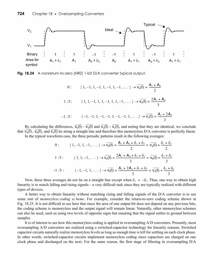
A more severe linearity limitation occurs if there is memory between output levels. For example, consider theideal and typical output signals for a two-level D/A converter, shown in Fig. 18.24. The area for each symbol isdefined to be the integral of the waveform over that symbol’s time period. Notice that for the typical output signal,the area is dependent on the past symbol and that difference is depicted using . As an illustrative example, con-sider the average voltage for three periodic patterns corresponding to average voltages of , , and when
and are volt.In the ideal case, both and are zero as the waveform is memoryless. Thus, the three periodic patterns ,, and result in the following averages:
Key Point: Multi-bit internal quantization improves stabil-ity and therefore is often used in high order modulators with low OSR. In A/D converters, it is combined with linearity enhancement techniques for the feedback DAC.
OSR
δi
0 1 3⁄ 1– 3⁄V1 V2 1±
δ1 δ2 01 3⁄ 1– 3⁄
c18.fm Page 723 Sunday, October 23, 2011 3:31 PM
724 Chapter 18 • Oversampling Converters
:
:
:
By calculating the differences, and , and noting that they are identical, we concludethat , , and lie along a straight line and therefore this memoryless D/A converter is perfectly linear.
In the typical waveform case, the three periodic patterns result in the following averages:
:
:
:
Now, these three averages do not lie on a straight line except when . Thus, one way to obtain highlinearity is to match falling and rising signals—a very difficult task since they are typically realized with differenttypes of devices.
A better way to obtain linearity without matching rising and falling signals of the D/A converter is to usesome sort of memoryless coding sc heme. For example, consider the return-to-zero coding scheme shown inFig. 18.25. It is not difficult to see here that since the area of one output bit does not depend on any previous bits,the coding scheme is memoryless and the output signal will remain linear. Naturally, other memoryless schemescan also be used, such as using two levels of opposite signs but ensuring that the signal settles to ground betweensamples.
It is of interest to see how this memoryless coding is applied in oversampling A/D converters. Presently, mostoversampling A/D converters are realized using a switched-capacitor technology for linearity reasons. Switchedcapacitor circuits naturally realize memoryless levels as long as enough time is left for settling on each clock phase.In other words, switched-capacitor circuits implement memoryless coding since capacitors are charged on oneclock phase and discharged on the next. For the same reason, the first stage of filtering in oversampling D/A
0 1 1 1 1 1 1 1 1, . . .–, ,–, ,–, ,–,{ } va t( ) A1 A0+
2------------------=→
Fig. 18.24 A nonreturn-to-zero (NRZ) 1-bit D/A converter typical output.
A1 δ1+ A1
1 1– 1– 1–1 1 1A0 δ2+ A0
V2
V1
Binary
Area forsymbol
A1 δ1+ A1 δ1+A0 δ2+
IdealTypical
1 3⁄ 1 1 1– 1 1 1– 1 1 1, . . .–, , , , , , , ,{ } vb t( ) 2A1 A0+
3---------------------=→
1– 3⁄ 1– 1– 1 1– 1– 1 1– 1– 1, . . ., , , , , , , ,{ } vc t( ) A1 2A0+
3---------------------=→
vb t( ) va t( )– va t( ) vc t( )–va t( ) vb t( ) vc t( )
0 1 1– 1 1, . . .–, , ,{ } vd t( ) A1 A0 δ1 δ2+ + +
2---------------------------------------- va t( ) δ1 δ2+
2----------------+= =→
1 3⁄ 1 1 1, . . .–, ,{ } ve t( ) 2A1 A0 δ1 δ2+ + +
3-------------------------------------------- vb t( ) δ1 δ2+
3----------------+= =→
1– 3⁄ 1– 1– 1, . . ., ,{ } vf t( ) A1 2A0 δ1 δ2+ + +
3-------------------------------------------- vc t( ) δ1 δ2+
3----------------+= =→
δ1 δ2–=
c18.fm Page 724 Sunday, October 23, 2011 3:31 PM
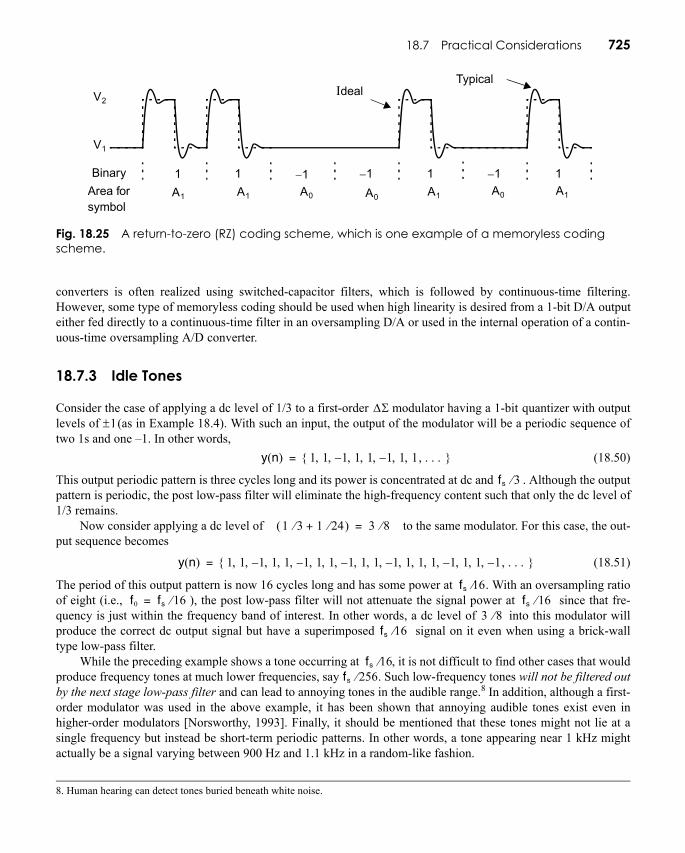
18.7 Practical Considerations 725
converters is often realized using switched-capacitor filters, which is followed by continuous-time filtering.However, some type of memoryless coding should be used when high linearity is desired from a 1-bit D/A outputeither fed directly to a continuous-time filter in an oversampling D/A or used in the internal operation of a contin-uous-time oversampling A/D converter.
18.7.3 Idle Tones
Consider the case of applying a dc level of 1/3 to a first-order modulator having a quantizer with outputlevels of (as in Example 18.4). With such an input, the output of the modulator will be a periodic sequence oftwo 1s and one –1. In other words,
(18.50)
This output periodic pattern is three cycles long and its power is concentrated at dc and . Although the outputpattern is periodic, the post low-pass filter will eliminate the high-frequency content such that only the dc level of1/3 remains.
Now consider applying a dc level of to the same modulator. For this case, the out-put sequence becomes
(18.51)
The period of this output pattern is now 16 cycles long and has some power at . With an oversampling ratioof eight (i.e., ), the post low-pass filter will not attenuate the signal power at since that fre-quency is just within the frequency band of interest. In other words, a dc level of into this modulator willproduce the correct dc output signal but have a superimposed signal on it even when using a brick-walltype low-pass filter.
While the preceding example shows a tone occurring at , it is not difficult to find other cases that wouldproduce frequency tones at much lower frequencies, say . Such low-frequency tones will not be filtered outby the next stage low-pass filter and can lead to annoying tones in the audible range.8 In addition, although a first-order modulator was used in the above example, it has been shown that annoying audible tones exist even inhigher-order modulators [Norsworthy, 1993]. Finally, it should be mentioned that these tones might not lie at asingle frequency but instead be short-term periodic patterns. In other words, a tone appearing near 1 kHz mightactually be a signal varying between 900 Hz and 1.1 kHz in a random-like fashion.
8. Human hearing can detect tones buried beneath white noise.
Fig. 18.25 A return-to-zero (RZ) coding scheme, which is one example of a memoryless coding scheme.
IdealTypical
A1 A1
1 1– 1– 1–1 1 1A0
V2
V1
Binary
Area forsymbol
A0 A1 A1A0
ΔΣ 1-bit1±
y n( ) 1 1 1– 1 1 1– 1 1, . . ., , , , , , ,{ }=
fs 3⁄
1 3⁄ 1 24⁄+( ) 3 8⁄=
y n( ) 1 1 1– 1 1 1– 1 1 1– 1 1 1– 1 1 1 1– 1 1 1, . . .–, , , , , , , , , , , , , , , , , ,{ }=
fs 16⁄f0 fs 16⁄= fs 16⁄
3 8⁄fs 16⁄
fs 16⁄fs 256⁄
c18.fm Page 725 Sunday, October 23, 2011 3:31 PM

726 Chapter 18 • Oversampling Converters
18.7.4 Dithering
One way to reduce the amount of idle tones in modulators is through the use of dithering. The term dithering hererefers to the act of introducing some random (or pseudo-random) signal into a modulator.
Assuming the random signal to be introduced has a white-noise type spec-trum, then the most suitable place to add the dithering signal is just before thequantizer, as shown in Fig. 18.26. The reason for adding it at this location is sothat the dithering signal becomes noise shaped in the same manner as the quan-tization noise, and thus a large amount of dithering can be added. Typically, thedithering signal is realized using some sort of pseudo-random number generatorwith only a few bits of resolution, but its total noise power is comparable to thequantization noise power. Thus, the use of dithering in a D/A converter wouldrequire a small additional digital adder, while a small D/A converter would beneeded in an oversampling A/D converter.
It should be noted that the use of dither to reduce idle tones is not an attempt to add noise to mask out thetones but instead breaks up the tones so that they never occur. However, since the noise power of the dithering sig-nal is similar to the quantization noise power, the use of dithering adds about 3 dB extra in-band noise and oftenrequires rechecking the modulator’s stability.
18.7.5 Opamp Gain
A switched-capacitor integrator with a finite opamp gain, , results in the integrator having a transfer function(see Problem 14.6) of
(18.52)
Assuming as is typical in oversampled converters, the pole has moved to the left of by an amount. With this knowledge, we can determine the new NTF zeros due to finite opamp gain by substituting
with . In other words, we substitute all ideal integrators with damped integrators and recalculate thetransfer functions. Such an approach results in the NTF zeros, which were located at for a low-pass design,to be moved to . Thus, the shaped quantization noise does not drop to zero at dc but instead levelsoff near dc. Such a zero near results in the 3-dB break frequency being approximately equal to rad/sample. Now, we note that the frequency band of interest, , should be greater than rad/sample since theshaped quantization noise is flat below that level. In other words, if is below where the quantization noise flattens
Key Point: The nonlinear dynamics of 1-bit oversampling modulators can result in idle tones within the signal band when applying dc or slowly-varying inputs. An additive pseudo-random dither signal can break up the tones but raises the noise floor.
Fig. 18.26 Adding dithering to a delta-sigma modulator. Note that the dithered signal is also noise shaped.
H z( )–
u n( ) y n( )
Quantizer
Dither signal
A
Vo z( )Vi z( )------------- C1
C2
------⎝ ⎠⎛ ⎞
1
z 1 C1
C2A----------+⎝ ⎠
⎛ ⎞ 1–
--------------------------------------
⎝ ⎠⎜ ⎟⎜ ⎟⎜ ⎟⎛ ⎞
–=
C2 C1≈ z 1=1 A⁄ z 1–
z 1 1 A⁄–( )–z 1=
z 1 1 A⁄–( )=z 1= 1 A⁄
f0 1 A⁄f0
c18.fm Page 726 Sunday, October 23, 2011 3:31 PM
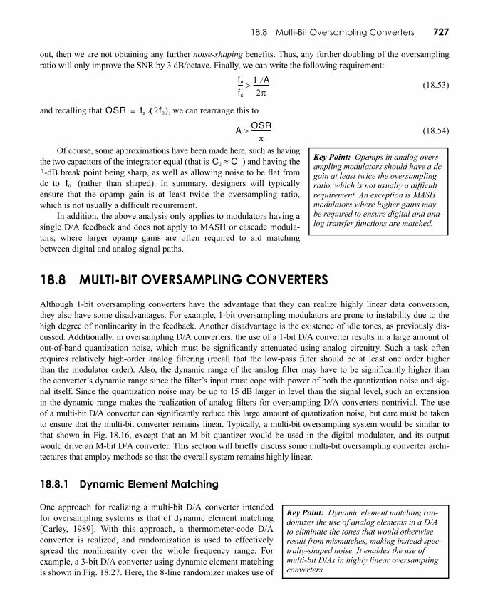
18.8 Multi-Bit Oversampling Converters 727
out, then we are not obtaining any further noise-shaping benefits. Thus, any further doubling of the oversamplingratio will only improve the SNR by 3 dB/octave. Finally, we can write the following requirement:
(18.53)
and recalling that , we can rearrange this to
(18.54)
Of course, some approximations have been made here, such as havingthe two capacitors of the integrator equal (that is ) and having the3-dB break point being sharp, as well as allowing noise to be flat fromdc to (rather than shaped). In summary, designers will typicallyensure that the opamp gain is at least twice the oversampling ratio,which is not usually a difficult requirement.
In addition, the above analysis only applies to modulators having asingle D/A feedback and does not apply to MASH or cascade modula-tors, where larger opamp gains are often required to aid matchingbetween digital and analog signal paths.
18.8 MULTI-BIT OVERSAMPLING CONVERTERSAlthough 1-bit oversampling converters have the advantage that they can realize highly linear data conversion,they also have some disadvantages. For example, 1-bit oversampling modulators are prone to instability due to thehigh degree of nonlinearity in the feedback. Another disadvantage is the existence of idle tones, as previously dis-cussed. Additionally, in oversampling D/A converters, the use of a 1-bit D/A converter results in a large amount ofout-of-band quantization noise, which must be significantly attenuated using analog circuitry. Such a task oftenrequires relatively high-order analog filtering (recall that the low-pass filter should be at least one order higherthan the modulator order). Also, the dynamic range of the analog filter may have to be significantly higher thanthe converter’s dynamic range since the filter’s input must cope with power of both the quantization noise and sig-nal itself. Since the quantization noise may be up to 15 dB larger in level than the signal level, such an extensionin the dynamic range makes the realization of analog filters for oversampling D/A converters nontrivial. The useof a multi-bit D/A converter can significantly reduce this large amount of quantization noise, but care must be takento ensure that the multi-bit converter remains linear. Typically, a multi-bit oversampling system would be similar tothat shown in Fig. 18.16, except that an M-bit quantizer would be used in the digital modulator, and its outputwould drive an M-bit D/A converter. This section will briefly discuss some multi-bit oversampling converter archi-tectures that employ methods so that the overall system remains highly linear.
18.8.1 Dynamic Element Matching
One approach for realizing a multi-bit D/A converter intendedfor oversampling systems is that of dynamic element matching[Carley, 1989]. With this approach, a thermometer-code D/Aconverter is realized, and randomization is used to effectivelyspread the nonlinearity over the whole frequency range. Forexample, a 3-bit D/A converter using dynamic element matchingis shown in Fig. 18.27. Here, the 8-line randomizer makes use of
f0
fs
--- 1 A⁄2π
----------->
OSR fs 2f0( )⁄=
A OSRπ
------------->
Key Point: Opamps in analog overs-ampling modulators should have a dc gain at least twice the oversampling ratio, which is not usually a difficult requirement. An exception is MASH modulators where higher gains may be required to ensure digital and ana-log transfer functions are matched.
C2 C1≈
f0
Key Point: Dynamic element matching ran-domizes the use of analog elements in a D/A to eliminate the tones that would otherwise result from mismatches, making instead spec-trally-shaped noise. It enables the use of multi-bit D/As in highly linear oversampling converters.
c18.fm Page 727 Sunday, October 23, 2011 3:31 PM
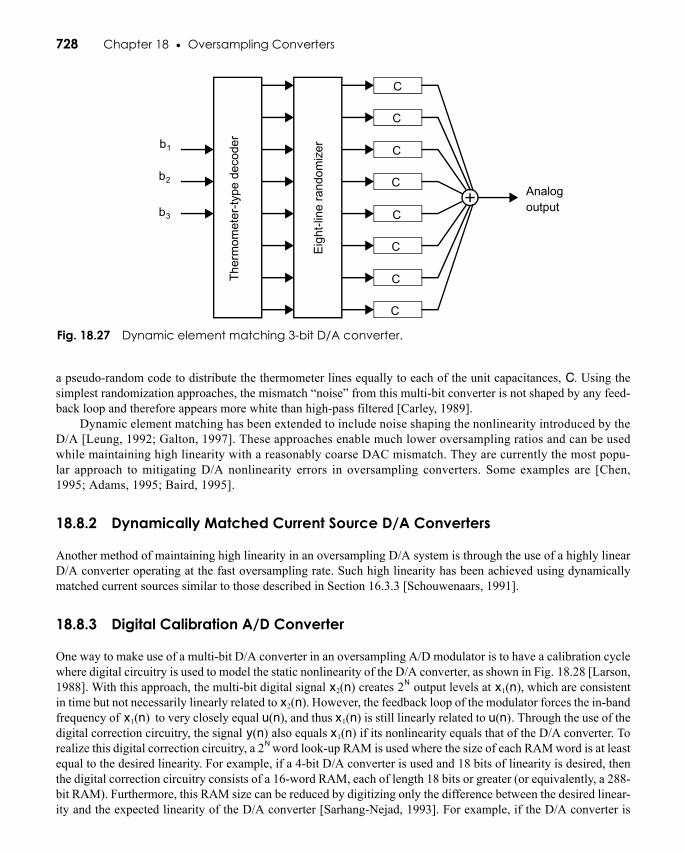
728 Chapter 18 • Oversampling Converters
a pseudo-random code to distribute the thermometer lines equally to each of the unit capacitances, . Using thesimplest randomization approaches, the mismatch “noise” from this multi-bit converter is not shaped by any feed-back loop and therefore appears more white than high-pass filtered [Carley, 1989].
Dynamic element matching has been extended to include noise shaping the nonlinearity introduced by theD/A [Leung, 1992; Galton, 1997]. These approaches enable much lower oversampling ratios and can be usedwhile maintaining high linearity with a reasonably coarse DAC mismatch. They are currently the most popu-lar approach to mitigating D/A nonlinearity errors in oversampling converters. Some examples are [Chen,1995; Adams, 1995; Baird, 1995].
18.8.2 Dynamically Matched Current Source D/A Converters
Another method of maintaining high linearity in an oversampling D/A system is through the use of a highly linearD/A converter operating at the fast oversampling rate. Such high linearity has been achieved using dynamicallymatched current sources similar to those described in Section 16.3.3 [Schouwenaars, 1991].
18.8.3 Digital Calibration A/D Converter
One way to make use of a multi-bit D/A converter in an oversampling A/D modulator is to have a calibration cyclewhere digital circuitry is used to model the static nonlinearity of the D/A converter, as shown in Fig. 18.28 [Larson,1988]. With this approach, the multi-bit digital signal creates output levels at , which are consistentin time but not necessarily linearly related to . However, the feedback loop of the modulator forces the in-bandfrequency of to very closely equal , and thus is still linearly related to . Through the use of thedigital correction circuitry, the signal also equals if its nonlinearity equals that of the D/A converter. Torealize this digital correction circuitry, a word look-up RAM is used where the size of each RAM word is at leastequal to the desired linearity. For example, if a 4-bit D/A converter is used and 18 bits of linearity is desired, thenthe digital correction circuitry consists of a 16-word RAM, each of length 18 bits or greater (or equivalently, a 288-bit RAM). Furthermore, this RAM size can be reduced by digitizing only the difference between the desired linear-ity and the expected linearity of the D/A converter [Sarhang-Nejad, 1993]. For example, if the D/A converter is
C
Fig. 18.27 Dynamic element matching 3-bit D/A converter.
C
C
C
C
C
C
C
CE
ight
-line
ran
dom
izer
The
rmom
eter
-typ
e de
code
rb1
b2
b3
Analogoutput
x2 n( ) 2N x1 n( )x2 n( )
x1 n( ) u n( ) x1 n( ) u n( )y n( ) x1 n( )
2N
c18.fm Page 728 Sunday, October 23, 2011 3:31 PM
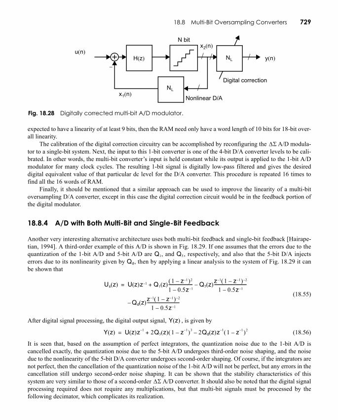
18.8 Multi-Bit Oversampling Converters 729
expected to have a linearity of at least 9 bits, then the RAM need only have a word length of 10 bits for 18-bit over-all linearity.
The calibration of the digital correction circuitry can be accomplished by reconfiguring the A/D modula-tor to a single-bit system. Next, the input to this 1-bit converter is one of the 4-bit D/A converter levels to be cali-brated. In other words, the multi-bit converter’s input is held constant while its output is applied to the 1-bit A/Dmodulator for many clock cycles. The resulting 1-bit signal is digitally low-pass filtered and gives the desireddigital equivalent value of that particular dc level for the D/A converter. This procedure is repeated 16 times tofind all the 16 words of RAM.
Finally, it should be mentioned that a similar approach can be used to improve the linearity of a multi-bitoversampling D/A converter, except in this case the digital correction circuit would be in the feedback portion ofthe digital modulator.
18.8.4 A/D with Both Multi-Bit and Single-Bit Feedback
Another very interesting alternative architecture uses both multi-bit feedback and single-bit feedback [Hairape-tian, 1994]. A third-order example of this A/D is shown in Fig. 18.29. If one assumes that the errors due to thequantization of the 1-bit A/D and 5-bit A/D are , and , respectively, and also that the 5-bit D/A injectserrors due to its nonlinearity given by , then by applying a linear analysis to the system of Fig. 18.29 it canbe shown that
(18.55)
After digital signal processing, the digital output signal, , is given by
(18.56)
It is seen that, based on the assumption of perfect integrators, the quantization noise due to the 1-bit A/D iscancelled exactly, the quantization noise due to the 5-bit A/D undergoes third-order noise shaping, and the noisedue to the nonlinearity of the 5-bit D/A converter undergoes second-order shaping. Of course, if the integrators arenot perfect, then the cancellation of the quantization noise of the 1-bit A/D will not be perfect, but any errors in thecancellation still undergo second-order noise shaping. It can be shown that the stability characteristics of thissystem are very similar to those of a second-order A/D converter. It should also be noted that the digital signalprocessing required does not require any multiplications, but that multi-bit signals must be processed by thefollowing decimator, which complicates its realization.
Fig. 18.28 Digitally corrected multi-bit A/D modulator.
H z( )–
u n( )y n( )NL
N bit
NL
Nonlinear D/A
Digital correction
x1 n( )
x2 n( )
ΔΣ
Q1 Q5
Qd
Us z( ) U z( )z 1– Q1 z( ) 1 z 1––( )2
1 0.5z 1––----------------------- Q5 z( )z 1– 1 z 1––( ) 2–
1 0.5z 1––-------------------------------–+=
Qd z( )z 1– 1 z 1––( ) 2–
1 0.5z 1––-------------------------------–
Y z( )
Y z( ) U z( )z 1– 2Q5 z( ) 1 z 1––( )3 2Qd z( )z 1– 1 z 1––( )2–+=
ΔΣ
c18.fm Page 729 Sunday, October 23, 2011 3:31 PM
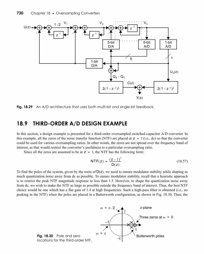
730 Chapter 18 • Oversampling Converters
18.9 THIRD-ORDER A/D DESIGN EXAMPLEIn this section, a design example is presented for a third-order oversampled switched-capacitor A/D converter. Inthis example, all the zeros of the noise transfer function (NTF) are placed at (i.e., dc) so that the convertercould be used for various oversampling ratios. In other words, the zeros are not spread over the frequency band ofinterest, as that would restrict the converter’s usefulness to a particular oversampling ratio.
Since all the zeros are assumed to be at , the NTF has the following form:
(18.57)
To find the poles of the system, given by the roots of , we need to ensure modulator stability while shaping asmuch quantization noise away from dc as possible. To ensure modulator stability, recall that a heuristic approachis to restrict the peak NTF magnitude response to less than 1.5. However, to shape the quantization noise awayfrom dc, we wish to make the NTF as large as possible outside the frequency band of interest. Thus, the best NTFchoice would be one which has a flat gain of 1.4 at high frequencies. Such a high-pass filter is obtained (i.e., nopeaking in the NTF) when the poles are placed in a Butterworth configuration, as shown in Fig. 18.30. Thus, the
Fig. 18.29 An A/D architecture that uses both multi-bit and single-bit feedback.
–
U z( )
Y z( )
z 1–
z 1–z 1– – –
V3V2V1
5-bitD/A
5-bitA/D
1-bitA/D
1-bitD/A
2 1 z 1––( )2 2 1 z 1––( )2
5 1
Us z( )Q5 Q1–
C z( )
1 2⁄
z 1=
z 1=
NTF z( ) z 1–( )3
D z( )------------------=
D z( )
Fig. 18.30 Pole and zero locations for the third-order NTF.
z-plane
–1
1
j
–j
ω 0=
ω π 2⁄=
ω π=
Three zeros at
Butterworth poles
c18.fm Page 730 Sunday, October 23, 2011 3:31 PM
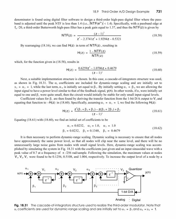
18.9 Third-Order A/D Design Example 731
denominator is found using digital filter software to design a third-order high-pass digital filter where the pass-band is adjusted until the peak NTF is less than 1.4 (i.e., ). Specifically, with a passband edge at
, a third-order Butterworth high-pass filter has a peak gain equal to 1.37, and thus the is given by
(18.58)
By rearranging (18.16), we can find in term of , resulting in
(18.59)
which, for the function given in (18.58), results in
(18.60)
Next, a suitable implementation structure is chosen. In this case, a cascade-of-integrators structure was used,as shown in Fig. 18.31. The coefficients are included for dynamic-range scaling and are initially set to
, while the last term, , is initially set equal to . By initially setting , we are allowing theinput signal to have a power level similar to that of the feedback signal, . In other words, if were initially setequal to one and were quite small, then the circuit would initially be stable for only small input-signal levels.
Coefficient values for are then found by deriving the transfer function from the 1-bit D/A output to andequating that function to in (18.60). Specifically, assuming , we find the following :
(18.61)
Equating (18.61) with (18.60), we find an initial set of coefficients to be
(18.62)
It is then necessary to perform dynamic-range scaling. Dynamic scaling is necessary to ensure that all nodeshave approximately the same power level, so that all nodes will clip near the same level, and there will be nounnecessarily large noise gains from nodes with small signal levels. Here, dynamic-range scaling was accom-plished by simulating the system in Fig. 18.31 with the coefficients just given and an input sinusoidal wave with apeak value of 0.7 at a frequency of . Following the simulation, the maximum values at nodes
were found to be 0.1256, 0.5108, and 1.004, respectively. To increase the output level of a node by a
NTF ejω( ) 1.4<fs 20⁄ NTF z( )
NTF z( ) z 1–( )3
z3 2.3741z2– 1.9294z 0.5321–+---------------------------------------------------------------------------------=
H z( ) NTF z( )
H z( ) 1 NTF z( )–
NTF z( )-----------------------------=
H z( ) 0.6259z2 1.0706z– 0.4679+
z 1–( )3----------------------------------------------------------------------=
Fig. 18.31 The cascade-of-integrators structure used to realize the third-order modulator. Note that coefficients are used for dynamic-range scaling and are initially set to and .αi α1 β1= α2 =α3 1=
1-bit D/A
–
u n( ) y n( )Quantizer
z 1–
z 1–z 1– – –
β1 β2 β3
α1 α2 α3 V3V2V1
Analog Digital
α i
α2 α3 1= = α1 β1 α1 β1=y n( ) α1
β1
β i V3
H z( )– α2 α3 1= = H z( )
H z( ) z2 β1 β2 β3+ +( ) z β2 2β3+( )– β3+
z 1–( )3------------------------------------------------------------------------------------=
α1 0.0232= , α2 1.0= , α3 1.0=
β1 0.0232= , β2 0.1348= , β3 0.4679=
π 256⁄ rad/sampleV1 V2 V3, ,
c18.fm Page 731 Sunday, October 23, 2011 3:31 PM
732 Chapter 18 • Oversampling Converters
factor , the input branches should be multiplied by , while the output branches should be divided by . Forexample, the maximum value of node is increased to unity by multiplying both and by anddividing by . Similarly, node is scaled by dividing and by 0.5108 and multiplying by 0.5108. Node was left unchanged, as its maximum value was already near unity. Such a procedure results inthe following final values for the coefficients.
(18.63)
Finally, the block diagram of Fig. 18.31 can be realized by the switched-capacitor circuit shown in Fig. 18.32to obtain the final oversampled A/D converter.
18.10 KEY POINTS• Oversampling converters relax the requirements placed on the analog circuitry at the expense of more compli-
cated digital circuitry. [p. 696]• Quantization with a step size “LSB” can be modeled as an additive quantization noise uniformly distributed
between –LSB/2 and +LSB/2 with a white power spectrum and total power of LSB2/12. [p. 697]
k k kV1 α1 β1 1 0.1256⁄
α2 1 0.1256⁄ V2 0.1256α2 β2 α3
V3
α′1 0.1847= , α′2 0.2459= , α′3 0.5108=
β′1 0.1847= , β′2 0.2639= , β′3 0.4679=
Fig. 18.32 A switched-capacitor realization of the third-order modulator example.
φ2a
φ1a
φ1a
φ1a
+VDAC
+VDACVDAC–
V– DAC
φ2a
φ2a
φ1a
φ2a
φ2a
φ1
φ2
φ2
φ1
φ2
φ2
φ1
φ2
φ2
φ1 φ1
φ2
φ2
φ1
φ1
φ2
φ2
φ1
φ2
α′1
α′1
α′2
α′2
α′3
α′3
CA 1=
CA 1=
CA 1=
CA 1=
CA 1=
CA 1=
β′3
β′3
β′2
β′2
β′1
β′1
+Vin
–
+V3
–
+V3–
φ1
+Vref– +VDAC
V– DAC
φ1
φ2
c18.fm Page 732 Sunday, October 23, 2011 3:31 PM
18.10 Key Points 733
• Oversampling a signal at OSR times the Nyquist rate, without spectrally shaping the quantization noise, resultsin a SNR enhancement of 10 log(OSR) dB. [p. 700]
• One-bit D/A converters are inherently linear. Hence, when combined with a high oversampling ratio, they canprovide a good signal to quantization noise and distortion ratio. [p. 702]
• To shape the spectrum of a quantization noise source, it is placed within a feedback loop whose response isdesigned to attenuate the quantization noise in the band of interest. [p. 704]
• Using a single integrator inside a DS modulator feedback loop places a zero at dc in the noise transfer functionproviding first-order noise shaping for low-pass signals. [p. 704]
• First-order noise shaping permits SQNR to increase by 1.5 bits/octave with respect to oversampling ratio, or 9dB for every doubling of OSR. [p. 706]
• Second-order noise shaping increases SQNR by 15 dB for each doubling of OSR, or equivalently by 1.5 bits/octave. [p. 708]
• The input signal power is often limited to well below the maximum quantizer swing to ensure stability, resultingin reduced SQNR. [p. 709]
• Oversampling A/D converters require additional digital low-pass filtering, but less analog anti-aliasingfiltering—often an desirable trade-off in integrated circuits. [p. 711]
• The linearity of oversampled A/D converters depends more strongly on the linearity of its internal D/A con-verter than on its internal quantizer. [p. 712]
• Oversampling D/A converters require a very linear but low-resolution internal D/A converter, and an analogsmoothing filter whose order should be at least one greater than that of the noise shaping and must have suffi-cient dynamic range to accommodate both signal and large quantization noise power at its input. [p. 713]
• In a multi-stage decimation filter, an initial lowpass filter removes much of the quantization noise. Its output isthen downsampled so that the remaining filtering can be performed at a lower clock frequency. [p. 715]
• In single-stage decimation, one filter operates on a low-resolution noise-shaped signal providing the decimatedoutput. Because of the high filter order, several time-interleaved filters may be used in parallel. [p. 717]
• Noise shaping with order L>2 offers the potential for further improvements in SQNR of 6L+3 dB/octave orL+0.5 bits/octave with respect to oversampling ratio. [p. 718]
• Interpolative higher-order modulators permit the arbitrary placement of noise transfer function zeros, offeringimproved SQNR performance compared to the placement of all zeros at dc, especially for relatively low OSR.However, it is nontrivial to guarantee stability for such structures, and they are therefore often combined withmulti-bit internal quantizers. [p. 718]
• Multi-stage noise shaping (MASH) oversampling converters cascade lower order modulators to realize high-order noise shaping. Since the constituent stages are each first- or second-order, it is easy to ensure stability.However, MASH converters require digital filtering whose coefficients are matched to those of analog circuitry.[p. 720]
• The stability of 1-bit modulators is not well understood, but as a rule of thumb keeping the peak magnituderesponse of the noise transfer function below 1.5 often results in a stable modulator. [p. 722]
• Multi-bit internal quantization improves stability and therefore is often used in high order modulators with lowOSR. In A/D converters, it is combined with linearity enhancement techniques for the feedback DAC. [p. 723]
• The nonlinear dynamics of 1-bit oversampling modulators can result in idle tones within the signal band whenapplying dc or slowly-varying inputs. An additive pseudo-random dither signal can break up the tones but raisesthe noise floor. [p. 726]
• Opamps in analog oversampling modulators should have a dc gain at least twice the oversampling ratio, whichis not usually a difficult requirement. An exception is MASH modulators where higher gains may be required toensure digital and analog transfer functions are matched. [p. 727]
c18.fm Page 733 Sunday, October 23, 2011 3:31 PM

734 Chapter 18 • Oversampling Converters
• Dynamic element matching randomizes the use of analog elements in a D/A to eliminate the tones that wouldotherwise result from mismatches, making instead spectrally-shaped noise. It enables the use of multi-bit D/Asin highly linear oversampling converters. [p. 727]
18.11 REFERENCESR. W. Adams and T. W. Kwan. “Data-Directed Scrambler for Multi-Bit Noise Shaping D/A Converters,” U.S. patent no.
5,404,142, April 1995.D. Anastassiou. “Error Diffusion Coding for A/D Conversion,” IEEE T rans. on C ircuits a nd Sys tems, Vol. 36, pp. 1175–1186,
September 1989.R. T. Baird and T. S. Fiez. “Improved Delta-Sigma DAC Linearity Using Data-Weighted Averaging,” Proc. IE EE Symp. on
Circuits and Systems, pp. 13–16, Seattle, 1995.B. E. Boser and B. A. Wooley. “The Design of Sigma-Delta Modulation Analog-To-Digital Converters,” IEEE J. of Solid-S tate
Circuits, Vol. 23, pp. 1298–1308, December 1988.J. C. Candy. “Decimation for Sigma-Delta Modulation,” IEEE Trans. Commun., Vol. 34, pp. 72–76, January 1986.J. C. Candy and G. C. Temes. “Oversampling Methods for A/D and D/A Conversion,” Oversampling D elta-Sigma D ata Conv ert-
ers, ed. J. C. Candy and G. C. Temes, IEEE Press, New York, 1992.L. R. Carley. “A Noise-Shaping Coder Topology for 15+ Bit Converters,” IEEE J. of Solid-S tate Circuits, Vol. 24, pp. 267–273,
April 1989.K. C.-H. Chao, S. Nadeem, W. L. Lee, and C. G. Sodini. “A Higher-Order Topology for Interpolative Modulators for Oversam-
pling A/D Converters,” IEEE Trans. on Circuits and Systems, Vol. 37, pp. 309–318, March 1990.F. Chen and B. H. Leung. “A High-Resolution Multibit Sigma-Delta Modulator with Individual Level Averaging,” IEEE J. of
Solid-State Circuits, Vol. 30, pp. 453–460, April 1995.J. Dattorro et al. “The Implementation of One-Stage Multirate 64:1 FIR Decimator for Use in One-Bit Sigma-Delta A/D Applica-
tions,” AES 7th Int. Conf., May 1989.P. Ferguson, Jr., et al. “An 18b 20kHz Dual Sigma-Delta A/D Converter,” Int. Solid-State Circuits Conf., February 1991.I. Galton. “Spectral shaping of circuit errors in digital-to-analog converters,” IEEE T rans. on C ircuits a nd Sy stems—II: An alog
and Digital Signal Processing, vol.44, pp. 808–817, Oct. 1997.A. Hairapetian and G. C. Temes. “A Dual-Quantization Multi-Bit Sigma-Delta Analog/Digital Converter,” IEEE I nt. Sy mp. on
Circuits and Systems, pp. 437–441, May 1994.A. Hairapetian, G. C. Temes, and Z. X. Zhang. “Multibit Sigma-Delta Modulator with Reduced Sensitivity to DAC Nonlinearity,”
Electron. Lett., Vol. 27, pp. 990–991, May 1991.S. A. Jantzi, W. M. Snelgrove, and P. F. Ferguson, Jr. “A Fourth-Order Bandpass Sigma-Delta Modulator,” IEEE J . of Solid-S tate
Circuits, Vol. 28, pp. 282–291, March 1993.P. Kiss, J. Silva, A. Wiesbauer, T. Sun, U.-K. Moon, J. T. Stonick, and G. C. Temes, “Adaptive digital correction of analog errors
in MASH ADCs—Part II: Correction using test-signal injection,” IEEE Trans. Circuits Syst. II, pp. 629–638, July 2000.L. E. Larson, T. Cataltepe, and G. C. Temes. “Multibit Oversampled A/D Converter with Digital Error Correction,” Elec-
tron. Lett., Vol. 24, pp. 1051–1052, August 1988.H. A. Leopold et al. “A Monolithic CMOS 20-b Analog-to-Digital Converter,” IEEE J. of S olid-State Circuits, Vol. 26, pp. 910–
916, July 1991.T. C. Leslie and B. Singh. “An Improved Sigma-Delta Modulator Architecture,” IEEE In t. Symp. on Circuits an d Sy stems,
pp. 372–375, May 1990.B. Leung, “Multibit sigma-delta A/D converters incorporating a novel class of dynamic element matching techniques,” IEEE
Trans. on Circuits and Systems—II: Analog and Digital Signal Processing, vol. 39, pp. 35–51, Jan. 1992.Y. Matsuya, et al. “A 16-bit Oversampling A-to-D Conversion Technology Using Triple-Integration Noise Shaping,” IEEE J . o f
Solid-State Circuits, Vol. 22, pp. 921–929, December 1987.S. Norsworthy. “Optimal Nonrecursive Noise-Shaping Filters for Oversampling Data Converters–Part I and II,” IEEE I nt. S ymp.
on Circuits and Systems, pp. 1353–1360, Chicago, May 1993.
Σ Δ–
c18.fm Page 734 Sunday, October 23, 2011 3:31 PM
18.12 Problems 735
T. Saramaki et al. “Multiplier-Free Decimator Algorithms for Super-Resolution Oversampled Converters,” IEEE In t. S ymp. onCircuits and Systems, pp. 3275–3278, New Orleans, May 1990.
M. Sarhang-Nejad and G. C. Temes, “A High-Resolution Multibit ADC with Digital Correction and Relaxed AmplifierRequirements,” IEEE J. of Solid-State Circuits, Vol. 28, pp. 648–660, June 1993.
H. J. Schouwenaars, D. W. J. Groeneveld, C. A. A. Bastiaansen, and H. A. H. Termeer. “An Oversampled Multibit CMOS D/AConverter for Digital Audio with 115-dB Dynamic Range,” IEEE J. of Solid-S tate Circuits, Vol. 26, pp. 1775–1780,December 1991.
R. Schreier. “An Empirical Study of High-Order Single-Bit Delta-Sigma Modulators,” IEEE Trans. on Circuits and Systems—II: Analogand Digital Signal Processing, Vol. 40, pp. 461–466, August 1993.
R. Schreier and W. M. Snelgrove. “Bandpass Sigma-Delta Modulation,” Electron. Le tt., Vol. 25, no. 23, pp. 1560–1561,November 9, 1989.
G. C. Temes, S. Shu, and R. Schreier. “Architectures for DACs,” in Oversampling Data Converters, ed. G. C. Temes,IEEE Press, 1996.
P. P. Vaidyanathan. Multirate Systems and Filte r Banks. Prentice Hall, Englewood Cliffs, New Jersey, 1993.
18.12 PROBLEMS
18.12.1 Section 18.1: Oversampling without Noise Shaping
18.1 A converter with no noise shaping exhibits a SNR of 40 dB over a 1-MHz signal bandwidth. By what factor must the sampling rate be increased (without noise shaping) to obtain a maximum SNR of 80 dB?
18.2 A white noise source has a power of 1 mW when sampled at . If the same signal is sampled at and the result low-pass filtered with a bandwidth of , what is the resulting noise power?
18.3 Given that an 8-bit A/D converter has a SNR of 50 dB but is linear to 12 bits, what is the sampling rate required to achieve 12 bits of accuracy using straight oversampling on a signal bandwidth of 1 MHz?
18.12.2 Section 18.2: Oversampling with Noise Shaping
18.4 Repeat Example 18.4, except use a dc input level of . At what frequency would a tone appear (relative to the sampling rate, )?
18.5 Repeat Example 18.4, except use a dc input level of to see if the internal state of the modulator saturates.18.6 Repeat Example 18.4, except use an input sequence of to see if the internal
state of the modulator saturates. This problem demonstrates that a large level input signal can be applied to a mod-ulator if its signal power resides at a frequency where the gain of is low.
18.7 Repeat Problem 18.3, assuming that the 8-bit A/D converter is placed inside a first-order delta-sigma modulator. What is the sampling rate if a second-order modulator is used?
18.8 Assuming a 1-bit modulator has an output signal of and the input sinusoidal signal is peak-to-peak, what is the ratio of the signal power to quantization noise power before any filtering is applied?
18.9 What does the block need to be in Fig. 18.13 in order that a second-order noise transfer function is real-ized equal to ?
18.10 Assume that the switched capacitor realization of the first-order A/D modulator in Fig. 18.9 introduces thermal noise at a rms input-referred level of . Using a one-bit quantizer, and allowing equal noise contributions from the thermal noise and quantization noise, find the required value of (at a temperature 300 K) and of in order to achieve an SNR of 90 dB.
18.11 Show a switched-capacitor modulator realizing the second-order modulator shown in Fig. 18.10.
ΣΔ
ΔΣ ΔΣ
fs 10 MHz=fs 100 MHz= fs 20⁄
1.2 3⁄fs
1.110 10– 10 10– 10 10, . . .–, , , , ,{ }
H z( )
1± 0.5±
G z( ) 1–1 z 1––( )2
2kT C⁄C OSR
c18.fm Page 735 Sunday, October 23, 2011 3:31 PM
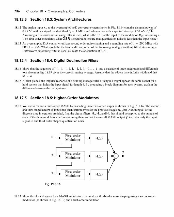
736 Chapter 18 • Oversampling Converters
18.12.3 Section 18.3: System Architectures
18.12 The analog input to the oversampled A/D converter system shown in Fig. 18.14 contains a signal power of within a signal bandwidth of and white noise with a spectral density of .
Assuming a first-order anti-aliasing filter is used, what is the SNR at the input to the modulator, ? Assuming a 1-bit first-order modulator, what is required to ensure that quantization noise is less than the input noise?
18.13 An oversampled D/A converter utilizes second order noise shaping and a sampling rate of with . What should be the bandwidth and order of the following analog smoothing filter? Assuming a
Butterworth smoothing filter is used, estimate the attenuation at .
18.12.4 Section 18.4: Digital Decimation Filters
18.14 Show that the sequence of into a cascade of three integrators and differentia-tors shown in Fig. 18.19 gives the correct running average. Assume that the adders have infinite width and that
.18.15 At first glance, the impulse response of a running average filter of length 4 might appear the same as that for a
hold system that holds the input signal for length 4. By producing a block diagram for each system, explain the difference between the two systems.
18.12.5 Section 18.5: Higher-Order Modulators
18.16 You are to realize a third-order MASH by cascading three first-order stages as shown in Fig. P18.16. The second and third stages accept as inputs the quantization errors of the previous stages, . Assuming all of the discrete-time integrators are ideal, find the digital filters , , and that should be applied to the outputs of each of the three modulators before summing them so that the overall MASH output includes only the input signal and third-order shaped quantization noise.
18.17 Show the block diagram for a MASH architecture that realizes third-order noise shaping using a second-order modulator (as shown in Fig. 18.10) and a first-order modulator.
xin
0.25 V2 f0 1 MHz= 50 nV Hz⁄xsh
OSR
fs 200 MHz=OSR 256=
fs 2⁄
1 1 1– 1 1 1– 1 1 1, . . .–, , , , , , , ,{ }
M 4=
e1 2, n( )H1 H2 H3
yu
First-orderModulator
First-orderModulator
First-orderModulator
e1
e2
u H1 z( )
H2 z( )
H3 z( )
Fig. P18.16
y
c18.fm Page 736 Sunday, October 23, 2011 3:31 PM
18.12 Problems 737
18.12.6 Section 18.6: Bandpass Oversampling Converters
18.18 Sketch the noise transfer function from 0 to 4 MHz for the second-order bandpass modulator shown in Fig. 18.23, assuming the sampling rate, , equals 4 MHz.
18.19 Show how the block diagram in Fig. 18.23 can be modified so that the bandpass modulator places zeros at rather than .
18.12.7 Section 18.7: Practical Considerations
18.20 Using the “typical” waveform pattern shown in Fig. 18.24, find the practical average outputs when , , and have been applied to the first-order modulator shown in Fig. 18.7.
18.21 A single-bit second-order oversampled A/D converter is to be realized with a SQNR of 80 dB. Estimate a lower bound on the required dc gain of the opamps that can be used in its implementation.
18.12.8 Section 18.8: Multi-Bit Oversampling Converters
18.22 We wish to model a nonlinear 2-bit D/A, with output levels given by {–0.61, –0.17, 0.25, 0.59} as an ideal D/A followed by an additive error, . Assuming that the four levels occur with equal probability, what is the power of the ideal D/A quantization noise, and what is the error power due to the nonlinearity, ?
18.23 Analyze the third-order modulator in Fig. 18.29, proving (18.55) and (18.56).
fs
fs± 8⁄fs± 4⁄
0 1 2⁄1– 2⁄
Qd
Qd
c18.fm Page 737 Sunday, October 23, 2011 3:31 PM
Recommended