MICROPROCESSOR
Prepared by R.Kavitha Page 1
QUESTION BANK
Unit 1
1. Explain the term Microprocessor. ( CO1-K2)
A microprocessor is a multipurpose, programmable logic device that receives binary
instructions from a storage device called memory accepts binary data as input and processes data
according to those instructions and provides result as output.
2. Classify the BUS. ( CO1-K2)
Bus: Group of wires carrying information.
Address bus: An address bus is a computer bus that is used to specify a physical address.
Data bus: It provides transportation for data.
Control bus: It carries signals that report the status of various devices.
3. Compare CMP and SUB instruction of 8086.( CO1-K2)
After execution of an instruction, CMP – It affects the flag SUB- It doesn’t affect the flag
4. What is an Assembler Directive? (CO1-K1)
Assembler directives help the assembler to correctly understand the assembly language
programs to prepare the codes. There are some instructions in the assembly language program
which are not part of processor instruction set. These instructions are instructions to the
assembler, linker and loader. These are called as Pseudo – operations or as Assembler directives.
5. Outline about operand and opcode. ( CO1-K2)
Operand – It specifies the type of operation to be performed.
Op code – data needs for completing the task
6. Compare Maskable and Nonmaskable interrupts.(CO1-K2)
The interrupts whose request can be either accepted or rejected by the processor are
called maskable interrupts. The interrupts whose request has to be definitely accepted (or
cannot be rejected) by the processor are called non-maskable interrupts.
7. What is Procedure?(CO1-K1)
The procedure is a group of instructions stored as a separate program in the memory and
it is called from the main program whenever required. The type of procedure depends on where

MICROPROCESSOR
Prepared by R.Kavitha Page 2
the procedure is stored in the memory. If it is in the same code segment where the main program
is stored then it is called “near procedure” otherwise it is referred to as far procedure.
8. What is Recursive procedure? (CO1-K1)
Recursive procedure is a procedure which calls itself. If the procedure is called 4 times,
then it is decremented by one after each procedure CALL and the procedure is called again and
again until it reaches zero.
9. Tell the different ways of interrupting processor. (CO1-K1)
The processor can be interrupted in the following ways:
i) by an external signal generated by a peripheral,
ii) by an internal signal generated b y a special instruction in the program,
iii) by an internal signal generated due to an exceptional condition which occurs while executing
an instruction. (For example, in 8086 processor, divide by zero is an exceptional condition which
initiates type 0 interrupt and such an interrupt is also called execution).
MICROPROCESSOR
Prepared by R.Kavitha Page 3
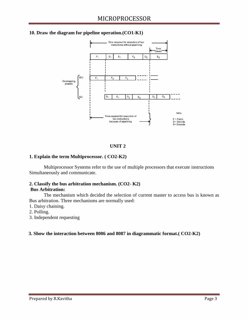
10. Draw the diagram for pipeline operation.(CO1-K1)
UNIT 2
1. Explain the term Multiprocessor. ( CO2-K2)
Multiprocessor Systems refer to the use of multiple processors that execute instructions
Simultaneously and communicate.
2. Classify the bus arbitration mechanism. (CO2- K2)
Bus Arbitration:
The mechanism which decided the selection of current master to access bus is known as
Bus arbitration. Three mechanisms are normally used:
1. Daisy chaining.
2. Polling.
3. Independent requesting
3. Show the interaction between 8086 and 8087 in diagrammatic format.( CO2-K2)

MICROPROCESSOR
Prepared by R.Kavitha Page 4
4. Outline about single step Interrupt. (CO2-K2)
• As in 8086, this is an internal interrupt that comes into action, if trap flag (TF) of 80286
is set.
• The CPU stops the execution after each instruction cycle. So, that the register contents
(including flag register), the program status word and memory, etc. may be examined at
the end of each instruction execution. This interrupt is useful for troubleshooting the
software. An interrupt vector type 01 is reserved for this interrupt.
5. Summarize the functions of the following signals in 80286. PEREG, PEACK. (CO2-K2)
• PEREG and PEACK (Processor Extension Request and Acknowledgement) Processor
extension refers to coprocessor. This pair of pins extends the memory management and
protection capabilities of 80286 to the processor extension 80287. The PEREQ input
requests the 80286 to perform a data operand transfer for a processor extension. The
PEACK active-low output indicates to the processor extension that the requested
operand is being transferred.
6. Summarize the functions of the following signals in 80286. HOLD and HLDA. (CO2-K2)
• HOLD and HLDA: This pair of pins is used by external bus masters to request for the
control of the system bus (HOLD) and to check whether the main processor has
granted the control (HLDA) or not, in the same way as it was in 8086.
7. Outline about single step Interrupt. (CO2-K2)
• As in 8086, this is an internal interrupt that comes into action, if trap flag (TF) of 80286
is set.

MICROPROCESSOR
Prepared by R.Kavitha Page 5
• The CPU stops the execution after each instruction cycle. So, that the register contents
(including flag register), the program status word and memory, etc. may be examined at
the end of each instruction execution. This interrupt is useful for troubleshooting the
software. An interrupt vector type 01 is reserved for this interrupt.
8. Short notes on Transcendental Instructions of 8087. (CO2-K2)
FPTAN - Compute the values for a ration of Y/X for an angle in ST. The angle must be
expressed in radians.
F2XM1 – Compute the function Y=2x – 1 for an X value in ST. Result will be stored in ST by
replacing X value.
9. What is the importance of IOPL signal in 80286? (CO2-K2)
IOPL – Input Output Privilege Level flags (bit D12 and D13)
IOPL is used in protected mode operation to select the privilege level for I/O devices.
10. What is the necessity of Memory Management unit?( CO2-K2)
The part of main memory in which the operating system and other system programs are
stored is not accessible to the users.
In view of this, an appropriate management of the memory system is required to ensure the
smooth execution of the running process and also to ensure their protection. The memory
management which is an important task of the operating system is supported by a hardware unit
called memory management unit.
Unit 3
1. What is the purpose of 8255? (CO3-K1)
The 8255 is a widely used, programmable parallel I/O device. It can be programmed to
transfer data under various conditions. It is flexible, versatile and economical (when multiple I/O
ports are required). It is an important general purpose I/O device that can be used with almost
any microprocessor.
2. What is the purpose of 8251? (CO3-K1)
8251 is a Universal Synchronous and Asynchronous Receiver and Transmitter
compatible with Intel‘s processors. This chip converts the parallel data into a serial stream of bits
suitable for serial transmission. It is also able to receive a serial stream of bits and convert it into
parallel data bytes to be read by a microprocessor.

MICROPROCESSOR
Prepared by R.Kavitha Page 6
3. Compare Linear and Absolute decoding. (CO3-K2)
In the absolute decoding technique the memory chip is selected only for the specified
logic level on the address lines: no other logic levels can select the chip. This address technique
is normally used in large memory systems.
In small system hardware for the decoding logic can be eliminated by using only required
number of addressing lines (not all). Other lines are simply ignored. This technique reduces the
cost of decoding circuit, but it has drawback of multiple addresses.
4. Summarize input and output port. (CO3-K2)
Input port: It is used to get the data from the input device such as keyboard and send it to the
microprocessor. The simplest form of the input port is a buffer.
5. Summarize about Left entry and right entry mode. (CO3-K2)
1. Left Entry Mode
In the Left entry mode, the data is entered from the left side of the display unit. Address 0 of
the display RAM contains the leftmost display character and address 15 of the RAM contains the
rightmost display character.
2. Right Entry Mode
• In the right entry mode, the first entry to be displayed is entered on the rightmost display.
The next entry is also placed in the right most display but after the previous display is
shifted left by one display position.
6. Outline about Mode 0 of 8255. (CO3-K2)
Mode 1: Input or Output with handshake
• In mode 1, handshake signals are exchanged between the microprocessor and peripherals
prior to data transfer.
• The ports (A and B) function as 8-bit I/O ports. They can be configured either as input or
output ports.
MICROPROCESSOR
Prepared by R.Kavitha Page 7
• Each port (Port A and Port B) uses 3 lines from port C as handshake signals. The
remaining two lines of port C can be used for simple I/O functions. Input and output data
are latched and Interrupt logic is supported.
7. What is cycle stealing? (CO3-K1)
• During any given bus cycle, one of the system components connected to the system
bus is given control of the bus. This component is said to be the master during that
cycle and the component it is communicating with is said to be the slave.
• The CPU with its bus control logic is normally the master, but other specially
designed components can gain control of the bus by sending a bus request to the CPU.
• After the current bus cycle is completed the CPU will return a bus grant signal and the
component sending the request will become the master.
• Taking control of the bus for a bus cycle is called cycle stealing.
8. How DMA operations are performed? (CO3-K1)
Following is the sequence of operations performed by a DMA .
• Initially, when any device has to send data between the device and the memory, the
device has to send DMA request (DRQ) to DMA controller.
• The DMA controller sends Hold request (HRQ) to the CPU and waits for the CPU to
assert the HLDA.
• Then the microprocessor tri-states all the data bus, address bus, and control bus. The CPU
leaves the control over bus and acknowledges the HOLD request through HLDA signal.
• Now the CPU is in HOLD state and the DMA controller has to manage the operations
over buses between the CPU, memory, and I/O devices.
• The chip support four DMA channels, i.e. four peripheral devices can independently
request for DMA data transfer through these channels at a time.
9. Compare Burst transfer and Hidden DMA. (CO3-K2)
Burst Transfer:
• To achieve block transfers, some DMAC's incorporate an automatic sequencing of the
value presented on the address bus. A register is used as a byte count, being
decremented for each byte transfer, and upon the byte count reaching zero, the DMAC
will release the bus. When the DMAC operates in burst mode, the CPU is halted for the
duration of the data transfer.
Hidden DMA:

MICROPROCESSOR
Prepared by R.Kavitha Page 8
• It is possible to perform hidden DMA, which is transparent to the normal operation of the
CPU. In other words, the bus is grabbed by the DMAC when the processor is not
using it. The DMAC monitors the execution of the processor, and when it recognises the
processor executing an instruction which has sufficient empty clock cycles to perform a
byte transfer; it waits till the processor is decoding the op code, then grabs the bus
during this time.
10. How does the master slave concept work? (CO3-K1)
MICROPROCESSOR
Prepared by R.Kavitha Page 9
Unit 4
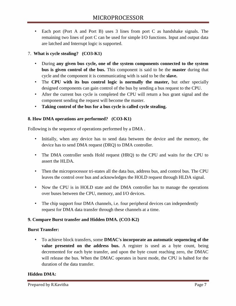
1. Compare Microprocessor and Microcontroller. (K2-CO4)
2. List out the application of 8051. (K1-CO4)
3. Summarize about CISC of 8051. (K2-CO4)

MICROPROCESSOR
Prepared by R.Kavitha Page 10
• Memory in those days was expensive. Bigger programs required more storage which
included more money. There was a need to reduce the number of instructions per
program. This was achieved by having multiple operations within single instruction.
• Multiple operations lead to many different kinds of instructions. Access to memory in
turn makes the instruction length variable and fetch-decode execute time unpredictable –
making it more complex. Thus hardware was made to understand the complexity of
instruction set.
• The computer having such instruction set was named as Complex Instruction Set
Computer (CISC). Intel 8051 is an example for CISC architecture.
4. Compare Von Neumann and Harward architecture. (K2-CO4)
5. What is an instruction cycle of 8051? (CO4-K1)
The time taken to complete any instruction is called as machine cycle or
instruction cycle. In 8051 one instruction cycle consists of 6 states or 12 clock cycles, instruction
cycle is also referred as Machine cycle.

MICROPROCESSOR
Prepared by R.Kavitha Page 11
6. What is Microcontroller?
A single chip computer or a CPU with all the peripherals like AM,ROM, I/O, Timers, ADCs,
etc on the same chip.
7. Show the internal RAM structure of 8051.
8. What are the use ofTimer/ Counter? (CO4-K1)
Timers/Counters are used generally for
• Time reference
• Creating delay
• Wave form properties measurement
• Periodic interrupt generation
• Waveform generation
MICROPROCESSOR
Prepared by R.Kavitha Page 12
9. Define an Instruction cycle
Instruction cycle is defined as the time required for completing the execution of an
instruction. The 8051 instruction cycle consists of one to four machine cycles.
10. What is an addressing mode? Short notes on Bit inherent addressing mode of 8051.
Various methods of accessing the data are called addressing modes.
Bit Inherent addressing mode” In this addressing, the address of the flag which contains the
operand, is implied in the opcode of the instruction.
• Eg. CLR C ; Clears the carry flag to 0
Unit 5
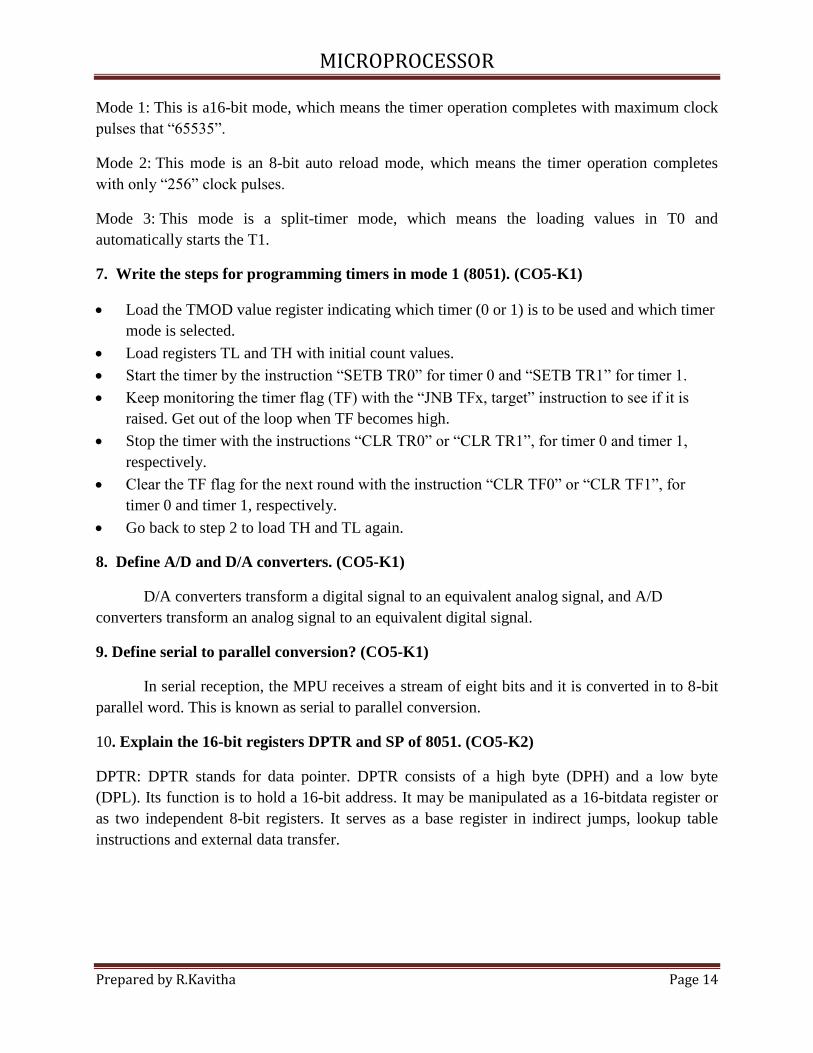
1. Summarize about interfacing of keyboard to the 8051. ( CO5 – K2)
Keyboards are organized in a matrix of rows and columns. The CPU accesses both rows
and columns through ports; therefore, with two 8-bit ports, an 8 x 8 matrix of keys can be
connected to a microprocessor. When a key is pressed, a row and a column make a contact;
otherwise, there is no connection between rows and columns.
2. Show the diagram of matrix keyboard connection to ports. (CO5-K2)
3. What are the steps have been taken while processing an interrupt? (CO5-K1)
1. It completes the execution of the current instruction.
2. PSW is pushed to stack.
3. PC content is pushed to stack.

MICROPROCESSOR
Prepared by R.Kavitha Page 13
4. Interrupt flag is reset.
5. PC is loaded with ISR address.
4. Show the structure of Interrupt Enable register of 8051.
5. Show the structure of Interrupt Priority register of 8051.
6. Summarize about modes of timer in 8051. (CO5-K2)
Mode 0: This is a 13-bit mode that means the timer operation completes with “8192” pulses.
MICROPROCESSOR
Prepared by R.Kavitha Page 14
Mode 1: This is a16-bit mode, which means the timer operation completes with maximum clock
pulses that “65535”.
Mode 2: This mode is an 8-bit auto reload mode, which means the timer operation completes
with only “256” clock pulses.
Mode 3: This mode is a split-timer mode, which means the loading values in T0 and
automatically starts the T1.
7. Write the steps for programming timers in mode 1 (8051). (CO5-K1)
• Load the TMOD value register indicating which timer (0 or 1) is to be used and which timer
mode is selected.
• Load registers TL and TH with initial count values.
• Start the timer by the instruction “SETB TR0” for timer 0 and “SETB TR1” for timer 1.
• Keep monitoring the timer flag (TF) with the “JNB TFx, target” instruction to see if it is
raised. Get out of the loop when TF becomes high.
• Stop the timer with the instructions “CLR TR0” or “CLR TR1”, for timer 0 and timer 1,
respectively.
• Clear the TF flag for the next round with the instruction “CLR TF0” or “CLR TF1”, for
timer 0 and timer 1, respectively.
• Go back to step 2 to load TH and TL again.
8. Define A/D and D/A converters. (CO5-K1)
D/A converters transform a digital signal to an equivalent analog signal, and A/D
converters transform an analog signal to an equivalent digital signal.
9. Define serial to parallel conversion? (CO5-K1)
In serial reception, the MPU receives a stream of eight bits and it is converted in to 8-bit
parallel word. This is known as serial to parallel conversion.
10. Explain the 16-bit registers DPTR and SP of 8051. (CO5-K2)
DPTR: DPTR stands for data pointer. DPTR consists of a high byte (DPH) and a low byte
(DPL). Its function is to hold a 16-bit address. It may be manipulated as a 16-bitdata register or
as two independent 8-bit registers. It serves as a base register in indirect jumps, lookup table
instructions and external data transfer.
Recommended