R
MicroBlazeProcessorReference GuideEmbeddedDevelopment Kit
EDK (v6.2) June 14, 2004

MicroBlaze Processor Reference Guide www.xilinx.com EDK (v6.2) June 14, 20041-800-255-7778
EDK (v6.2) June 14, 2004 www.xilinx.com MicroBlaze Processor Reference Guide1-800-255-7778
"Xilinx" and the Xilinx logo shown above are registered trademarks of Xilinx, Inc. Any rights not expressly granted herein are reserved.
CoolRunner, RocketChips, Rocket IP, Spartan, StateBENCH, StateCAD, Virtex, XACT, XC2064, XC3090, XC4005, and XC5210 areregistered trademarks of Xilinx, Inc.
The shadow X shown above is a trademark of Xilinx, Inc.
ACE Controller, ACE Flash, A.K.A. Speed, Alliance Series, AllianceCORE, Bencher, ChipScope, Configurable Logic Cell, COREGenerator, CoreLINX, Dual Block, EZTag, Fast CLK, Fast CONNECT, Fast FLASH, FastMap, Fast Zero Power, Foundation, GigabitSpeeds...and Beyond!, HardWire, HDL Bencher, IRL, J Drive, JBits, LCA, LogiBLOX, Logic Cell, LogiCORE, LogicProfessor, MicroBlaze,MicroVia, MultiLINX, NanoBlaze, PicoBlaze, PLUSASM, PowerGuide, PowerMaze, QPro, Real-PCI, Rocket I/O, SelectI/O, SelectRAM,SelectRAM+, Silicon Xpresso, Smartguide, Smart-IP, SmartSearch, SMARTswitch, System ACE, Testbench In A Minute, TrueMap, UIM,VectorMaze, VersaBlock, VersaRing, Virtex-II Pro, Virtex-II EasyPath, Wave Table, WebFITTER, WebPACK, WebPOWERED, XABEL,XACT-Floorplanner, XACT-Performance, XACTstep Advanced, XACTstep Foundry, XAM, XAPP, X-BLOX +, XC designated products,XChecker, XDM, XEPLD, Xilinx Foundation Series, Xilinx XDTV, Xinfo, XSI, XtremeDSP and ZERO+ are trademarks of Xilinx, Inc.
The Programmable Logic Company is a service mark of Xilinx, Inc.
All other trademarks are the property of their respective owners.
Xilinx, Inc. does not assume any liability arising out of the application or use of any product described or shown herein; nor does it conveyany license under its patents, copyrights, or maskwork rights or any rights of others. Xilinx, Inc. reserves the right to make changes, at anytime, in order to improve reliability, function or design and to supply the best product possible. Xilinx, Inc. will not assume responsibility forthe use of any circuitry described herein other than circuitry entirely embodied in its products. Xilinx provides any design, code, orinformation shown or described herein "as is." By providing the design, code, or information as one possible implementation of a feature,application, or standard, Xilinx makes no representation that such implementation is free from any claims of infringement. You areresponsible for obtaining any rights you may require for your implementation. Xilinx expressly disclaims any warranty whatsoever withrespect to the adequacy of any such implementation, including but not limited to any warranties or representations that the implementationis free from claims of infringement, as well as any implied warranties of merchantability or fitness for a particular purpose. Xilinx, Inc. devicesand products are protected under U.S. Patents. Other U.S. and foreign patents pending. Xilinx, Inc. does not represent that devices shownor products described herein are free from patent infringement or from any other third party right. Xilinx, Inc. assumes no obligation tocorrect any errors contained herein or to advise any user of this text of any correction if such be made. Xilinx, Inc. will not assume anyliability for the accuracy or correctness of any engineering or software support or assistance provided to a user.
Xilinx products are not intended for use in life support appliances, devices, or systems. Use of a Xilinx product in such applications withoutthe written consent of the appropriate Xilinx officer is prohibited.
The contents of this manual are owned and copyrighted by Xilinx. Copyright 1994-2002 Xilinx, Inc. All Rights Reserved. Except as statedherein, none of the material may be copied, reproduced, distributed, republished, downloaded, displayed, posted, or transmitted in any formor by any means including, but not limited to, electronic, mechanical, photocopying, recording, or otherwise, without the prior written consentof Xilinx. Any unauthorized use of any material contained in this manual may violate copyright laws, trademark laws, the laws of privacy andpublicity, and communications regulations and statutes.
R
MicroBlaze Processor Reference Guide www.xilinx.com EDK (v6.2) June 14, 20041-800-255-7778
MicroBlaze Processor Reference GuideEDK (v6.2) June 14, 2004
The following table shows the revision history for this document.
Version Revision
08/07/00 1.0 Xilinx EDK (Embedded Processor Development Kit) release.
MicroBlaze Processor Reference Guide www.xilinx.com 5EDK (v6.2) December 9, 2003 1-800-255-7778
Preface: About This GuideManual Contents . . . . . . . . . . . . . . . . . . . . . . . . . . . . . . . . . . . . . . . . . . . . . . . . . . . . . . . . . . . . . 7Additional Resources . . . . . . . . . . . . . . . . . . . . . . . . . . . . . . . . . . . . . . . . . . . . . . . . . . . . . . . . 7Conventions . . . . . . . . . . . . . . . . . . . . . . . . . . . . . . . . . . . . . . . . . . . . . . . . . . . . . . . . . . . . . . . . . 8
Typographical . . . . . . . . . . . . . . . . . . . . . . . . . . . . . . . . . . . . . . . . . . . . . . . . . . . . . . . . . . . . . 8Online Document . . . . . . . . . . . . . . . . . . . . . . . . . . . . . . . . . . . . . . . . . . . . . . . . . . . . . . . . . . 9
Chapter 1: MicroBlaze ArchitectureSummary . . . . . . . . . . . . . . . . . . . . . . . . . . . . . . . . . . . . . . . . . . . . . . . . . . . . . . . . . . . . . . . . . . . 11Overview . . . . . . . . . . . . . . . . . . . . . . . . . . . . . . . . . . . . . . . . . . . . . . . . . . . . . . . . . . . . . . . . . . . 11
Features . . . . . . . . . . . . . . . . . . . . . . . . . . . . . . . . . . . . . . . . . . . . . . . . . . . . . . . . . . . . . . . . . 11Instructions . . . . . . . . . . . . . . . . . . . . . . . . . . . . . . . . . . . . . . . . . . . . . . . . . . . . . . . . . . . . . . . . . 12Registers . . . . . . . . . . . . . . . . . . . . . . . . . . . . . . . . . . . . . . . . . . . . . . . . . . . . . . . . . . . . . . . . . . . . 16
General Purpose Registers . . . . . . . . . . . . . . . . . . . . . . . . . . . . . . . . . . . . . . . . . . . . . . . . . 16Special Purpose Registers . . . . . . . . . . . . . . . . . . . . . . . . . . . . . . . . . . . . . . . . . . . . . . . . . . 17
Pipeline . . . . . . . . . . . . . . . . . . . . . . . . . . . . . . . . . . . . . . . . . . . . . . . . . . . . . . . . . . . . . . . . . . . . . 19Pipeline Architecture . . . . . . . . . . . . . . . . . . . . . . . . . . . . . . . . . . . . . . . . . . . . . . . . . . . . . . 19Branches. . . . . . . . . . . . . . . . . . . . . . . . . . . . . . . . . . . . . . . . . . . . . . . . . . . . . . . . . . . . . . . . . 20
Load/Store Architecture . . . . . . . . . . . . . . . . . . . . . . . . . . . . . . . . . . . . . . . . . . . . . . . . . . . . . 20Interrupts, Exceptions and Breaks . . . . . . . . . . . . . . . . . . . . . . . . . . . . . . . . . . . . . . . . . . . 21
Interrupts . . . . . . . . . . . . . . . . . . . . . . . . . . . . . . . . . . . . . . . . . . . . . . . . . . . . . . . . . . . . . . . . 21Exceptions . . . . . . . . . . . . . . . . . . . . . . . . . . . . . . . . . . . . . . . . . . . . . . . . . . . . . . . . . . . . . . . 22Breaks . . . . . . . . . . . . . . . . . . . . . . . . . . . . . . . . . . . . . . . . . . . . . . . . . . . . . . . . . . . . . . . . . . . 22
Instruction Cache . . . . . . . . . . . . . . . . . . . . . . . . . . . . . . . . . . . . . . . . . . . . . . . . . . . . . . . . . . . 23Overview . . . . . . . . . . . . . . . . . . . . . . . . . . . . . . . . . . . . . . . . . . . . . . . . . . . . . . . . . . . . . . . . 23Cache Organization . . . . . . . . . . . . . . . . . . . . . . . . . . . . . . . . . . . . . . . . . . . . . . . . . . . . . . . 23Cache Operation . . . . . . . . . . . . . . . . . . . . . . . . . . . . . . . . . . . . . . . . . . . . . . . . . . . . . . . . . . 24Software . . . . . . . . . . . . . . . . . . . . . . . . . . . . . . . . . . . . . . . . . . . . . . . . . . . . . . . . . . . . . . . . . 25LMB Memory . . . . . . . . . . . . . . . . . . . . . . . . . . . . . . . . . . . . . . . . . . . . . . . . . . . . . . . . . . . . 26
Data Cache . . . . . . . . . . . . . . . . . . . . . . . . . . . . . . . . . . . . . . . . . . . . . . . . . . . . . . . . . . . . . . . . . . 26Overview . . . . . . . . . . . . . . . . . . . . . . . . . . . . . . . . . . . . . . . . . . . . . . . . . . . . . . . . . . . . . . . . 26Cache Organization . . . . . . . . . . . . . . . . . . . . . . . . . . . . . . . . . . . . . . . . . . . . . . . . . . . . . . . 26Cache Operation . . . . . . . . . . . . . . . . . . . . . . . . . . . . . . . . . . . . . . . . . . . . . . . . . . . . . . . . . . 27Software . . . . . . . . . . . . . . . . . . . . . . . . . . . . . . . . . . . . . . . . . . . . . . . . . . . . . . . . . . . . . . . . . 28LMB Memory . . . . . . . . . . . . . . . . . . . . . . . . . . . . . . . . . . . . . . . . . . . . . . . . . . . . . . . . . . . . 28
Fast Simplex Link Interface . . . . . . . . . . . . . . . . . . . . . . . . . . . . . . . . . . . . . . . . . . . . . . . . . 28FSL Read Instructions . . . . . . . . . . . . . . . . . . . . . . . . . . . . . . . . . . . . . . . . . . . . . . . . . . . . . 29FSL Write Instructions . . . . . . . . . . . . . . . . . . . . . . . . . . . . . . . . . . . . . . . . . . . . . . . . . . . . . 30
Debug Interface . . . . . . . . . . . . . . . . . . . . . . . . . . . . . . . . . . . . . . . . . . . . . . . . . . . . . . . . . . . . . 30Debugging Features . . . . . . . . . . . . . . . . . . . . . . . . . . . . . . . . . . . . . . . . . . . . . . . . . . . . . . . 31
Chapter 2: MicroBlaze Bus InterfacesSummary . . . . . . . . . . . . . . . . . . . . . . . . . . . . . . . . . . . . . . . . . . . . . . . . . . . . . . . . . . . . . . . . . . . 33
Table of Contents
6 www.xilinx.com MicroBlaze Processor Reference Guide1-800-255-7778 EDK (v6.2) December 9, 2003
R
Overview . . . . . . . . . . . . . . . . . . . . . . . . . . . . . . . . . . . . . . . . . . . . . . . . . . . . . . . . . . . . . . . . . . . 33Features . . . . . . . . . . . . . . . . . . . . . . . . . . . . . . . . . . . . . . . . . . . . . . . . . . . . . . . . . . . . . . . . . 33
Bus Configurations . . . . . . . . . . . . . . . . . . . . . . . . . . . . . . . . . . . . . . . . . . . . . . . . . . . . . . . . . 33Typical Peripheral Placement. . . . . . . . . . . . . . . . . . . . . . . . . . . . . . . . . . . . . . . . . . . . . . . 35
Bit and Byte Labeling . . . . . . . . . . . . . . . . . . . . . . . . . . . . . . . . . . . . . . . . . . . . . . . . . . . . . . . 43Core I/O . . . . . . . . . . . . . . . . . . . . . . . . . . . . . . . . . . . . . . . . . . . . . . . . . . . . . . . . . . . . . . . . . . . . 43Bus Organization . . . . . . . . . . . . . . . . . . . . . . . . . . . . . . . . . . . . . . . . . . . . . . . . . . . . . . . . . . . 45
OPB Bus Configuration . . . . . . . . . . . . . . . . . . . . . . . . . . . . . . . . . . . . . . . . . . . . . . . . . . . . 45LMB Bus Definition . . . . . . . . . . . . . . . . . . . . . . . . . . . . . . . . . . . . . . . . . . . . . . . . . . . . . . . 49LMB Bus Operations . . . . . . . . . . . . . . . . . . . . . . . . . . . . . . . . . . . . . . . . . . . . . . . . . . . . . . 50Read and Write Data Steering . . . . . . . . . . . . . . . . . . . . . . . . . . . . . . . . . . . . . . . . . . . . . . 53FSL Bus Operation . . . . . . . . . . . . . . . . . . . . . . . . . . . . . . . . . . . . . . . . . . . . . . . . . . . . . . . . 54
Debug Interface . . . . . . . . . . . . . . . . . . . . . . . . . . . . . . . . . . . . . . . . . . . . . . . . . . . . . . . . . . . . . 56Implementation . . . . . . . . . . . . . . . . . . . . . . . . . . . . . . . . . . . . . . . . . . . . . . . . . . . . . . . . . . . . . 57
Parameterization . . . . . . . . . . . . . . . . . . . . . . . . . . . . . . . . . . . . . . . . . . . . . . . . . . . . . . . . . 57
Chapter 3: MicroBlaze EndiannessDefinitions . . . . . . . . . . . . . . . . . . . . . . . . . . . . . . . . . . . . . . . . . . . . . . . . . . . . . . . . . . . . . . . . . 59Bit Naming Conventions . . . . . . . . . . . . . . . . . . . . . . . . . . . . . . . . . . . . . . . . . . . . . . . . . . . . 59Data Types and Endianness . . . . . . . . . . . . . . . . . . . . . . . . . . . . . . . . . . . . . . . . . . . . . . . . . 59VHDL Example . . . . . . . . . . . . . . . . . . . . . . . . . . . . . . . . . . . . . . . . . . . . . . . . . . . . . . . . . . . . . 61
BRAM – LMB Example . . . . . . . . . . . . . . . . . . . . . . . . . . . . . . . . . . . . . . . . . . . . . . . . . . . . 61BRAM – OPB Example . . . . . . . . . . . . . . . . . . . . . . . . . . . . . . . . . . . . . . . . . . . . . . . . . . . . 63
Chapter 4: MicroBlaze Application Binary InterfaceScope . . . . . . . . . . . . . . . . . . . . . . . . . . . . . . . . . . . . . . . . . . . . . . . . . . . . . . . . . . . . . . . . . . . . . . . 67Data Types . . . . . . . . . . . . . . . . . . . . . . . . . . . . . . . . . . . . . . . . . . . . . . . . . . . . . . . . . . . . . . . . . . 67Register Usage Conventions . . . . . . . . . . . . . . . . . . . . . . . . . . . . . . . . . . . . . . . . . . . . . . . . . 67Stack Convention . . . . . . . . . . . . . . . . . . . . . . . . . . . . . . . . . . . . . . . . . . . . . . . . . . . . . . . . . . . 69
Calling Convention . . . . . . . . . . . . . . . . . . . . . . . . . . . . . . . . . . . . . . . . . . . . . . . . . . . . . . . 70Memory Model . . . . . . . . . . . . . . . . . . . . . . . . . . . . . . . . . . . . . . . . . . . . . . . . . . . . . . . . . . . . . 70
Small data area . . . . . . . . . . . . . . . . . . . . . . . . . . . . . . . . . . . . . . . . . . . . . . . . . . . . . . . . . . . 70Data area . . . . . . . . . . . . . . . . . . . . . . . . . . . . . . . . . . . . . . . . . . . . . . . . . . . . . . . . . . . . . . . . 71Common un-initialized area. . . . . . . . . . . . . . . . . . . . . . . . . . . . . . . . . . . . . . . . . . . . . . . . 71Literals or constants . . . . . . . . . . . . . . . . . . . . . . . . . . . . . . . . . . . . . . . . . . . . . . . . . . . . . . . 71
Interrupt and Exception Handling . . . . . . . . . . . . . . . . . . . . . . . . . . . . . . . . . . . . . . . . . . . 71
Chapter 5: MicroBlaze Instruction Set ArchitectureSummary . . . . . . . . . . . . . . . . . . . . . . . . . . . . . . . . . . . . . . . . . . . . . . . . . . . . . . . . . . . . . . . . . . . 73Notation . . . . . . . . . . . . . . . . . . . . . . . . . . . . . . . . . . . . . . . . . . . . . . . . . . . . . . . . . . . . . . . . . . . . 73Formats . . . . . . . . . . . . . . . . . . . . . . . . . . . . . . . . . . . . . . . . . . . . . . . . . . . . . . . . . . . . . . . . . . . . . 74Instructions . . . . . . . . . . . . . . . . . . . . . . . . . . . . . . . . . . . . . . . . . . . . . . . . . . . . . . . . . . . . . . . . . 74
MicroBlaze Processor Reference Guide www.xilinx.com 7EDK (v6.2) December 9, 2003 1-800-255-7778
R
Preface
About This Guide
Welcome to the MicroBlaze Processor Reference Guide. This document providesinformation about the 32-bit soft processor, MicroBlaze, included in the EmbeddedProcessor Development Kit (EDK). The document is meant as a guide to the MicroBlazehardware and software architecture.
Manual ContentsThis manual discusses the following topics specific to MicroBlaze soft processor:
• Core Architecture
• Bus Interfaces and Endieness
• Application Binary Interface
• Instruction Set Architecture
Additional ResourcesFor additional information, go to http://support.xilinx.com. The following table listssome of the resources you can access from this website. You can also directly access theseresources using the provided URLs.
Resource Description/URL
Tutorials Tutorials covering Xilinx design flows, from design entry toverification and debugging
http://support.xilinx.com/support/techsup/tutorials/index.htm
Answer Browser Database of Xilinx solution records
http://support.xilinx.com/xlnx/xil_ans_browser.jsp
Application Notes Descriptions of device-specific design techniques and approaches
http://support.xilinx.com/apps/appsweb.htm
Data Book Pages from The Programmable Logic Data Book, which containsdevice-specific information on Xilinx device characteristics,including readback, boundary scan, configuration, length count,and debugging
http://support.xilinx.com/partinfo/databook.htm
Problem Solvers Interactive tools that allow you to troubleshoot your design issues
http://support.xilinx.com/support/troubleshoot/psolvers.htm
8 www.xilinx.com MicroBlaze Processor Reference Guide1-800-255-7778 EDK (v6.2) December 9, 2003
Preface: About This GuideR
ConventionsThis document uses the following conventions. An example illustrates each convention.
TypographicalThe following typographical conventions are used in this document:
Tech Tips Latest news, design tips, and patch information for the Xilinxdesign environment
http://www.support.xilinx.com/xlnx/xil_tt_home.jsp
GNU Manuals The entire set of GNU manuals
http://www.gnu.org/manual
Resource Description/URL
Convention Meaning or Use Example
Courier fontMessages, prompts, andprogram files that the systemdisplays
speed grade: - 100
Courier boldLiteral commands that youenter in a syntactical statement ngdbuild design_name
Helvetica bold
Commands that you selectfrom a menu File → Open
Keyboard shortcuts Ctrl+C
Italic font
Variables in a syntaxstatement for which you mustsupply values
ngdbuild design_name
References to other manualsSee the Development SystemReference Guide for moreinformation.
Emphasis in textIf a wire is drawn so that itoverlaps the pin of a symbol,the two nets are not connected.
Square brackets [ ]
An optional entry orparameter. However, in busspecifications, such asbus[7:0], they are required.
ngdbuild [option_name]design_name
Braces { } A list of items from which youmust choose one or more lowpwr ={on|off}
Vertical bar | Separates items in a list ofchoices lowpwr ={on|off}
MicroBlaze Processor Reference Guide www.xilinx.com 9EDK (v6.2) December 9, 2003 1-800-255-7778
ConventionsR
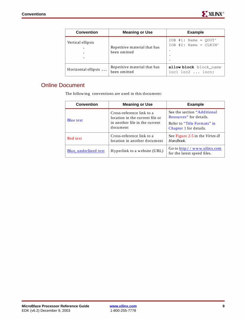
Online DocumentThe following conventions are used in this document:
Vertical ellipsis...
Repetitive material that hasbeen omitted
IOB #1: Name = QOUT’IOB #2: Name = CLKIN’...
Horizontal ellipsis . . .Repetitive material that hasbeen omitted
allow block block_nameloc1 loc2 ... locn;
Convention Meaning or Use Example
Convention Meaning or Use Example
Blue text
Cross-reference link to alocation in the current file orin another file in the currentdocument
See the section “AdditionalResources” for details.
Refer to “Title Formats” inChapter 1 for details.
Red text Cross-reference link to alocation in another document
See Figure 2-5 in the Virtex-IIHandbook.
Blue, underlined text Hyperlink to a website (URL) Go to http://www.xilinx.comfor the latest speed files.

10 www.xilinx.com MicroBlaze Processor Reference Guide1-800-255-7778 EDK (v6.2) December 9, 2003
Preface: About This GuideR
MicroBlaze Processor Reference Guide www.xilinx.com 11EDK (v6.2) December 9, 2003 1-800-255-7778
R
Chapter 1
MicroBlaze Architecture
SummaryThis document describes the architecture for the MicroBlaze™ 32-bit soft processor core.
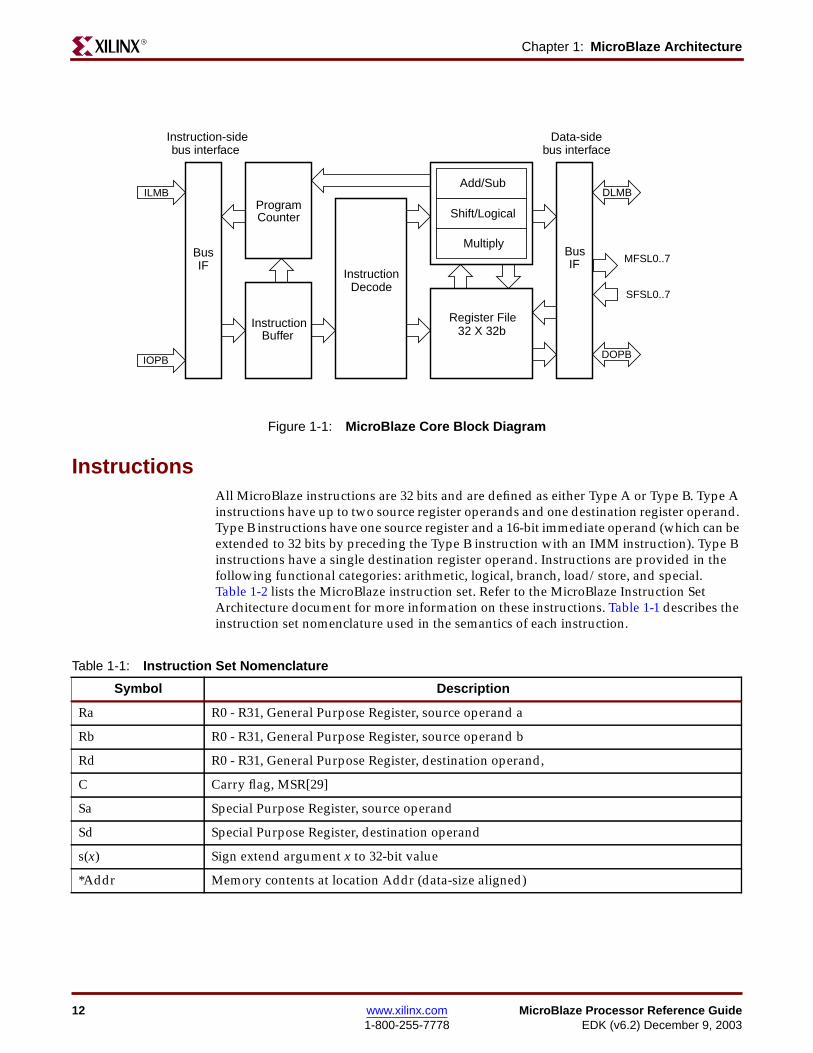
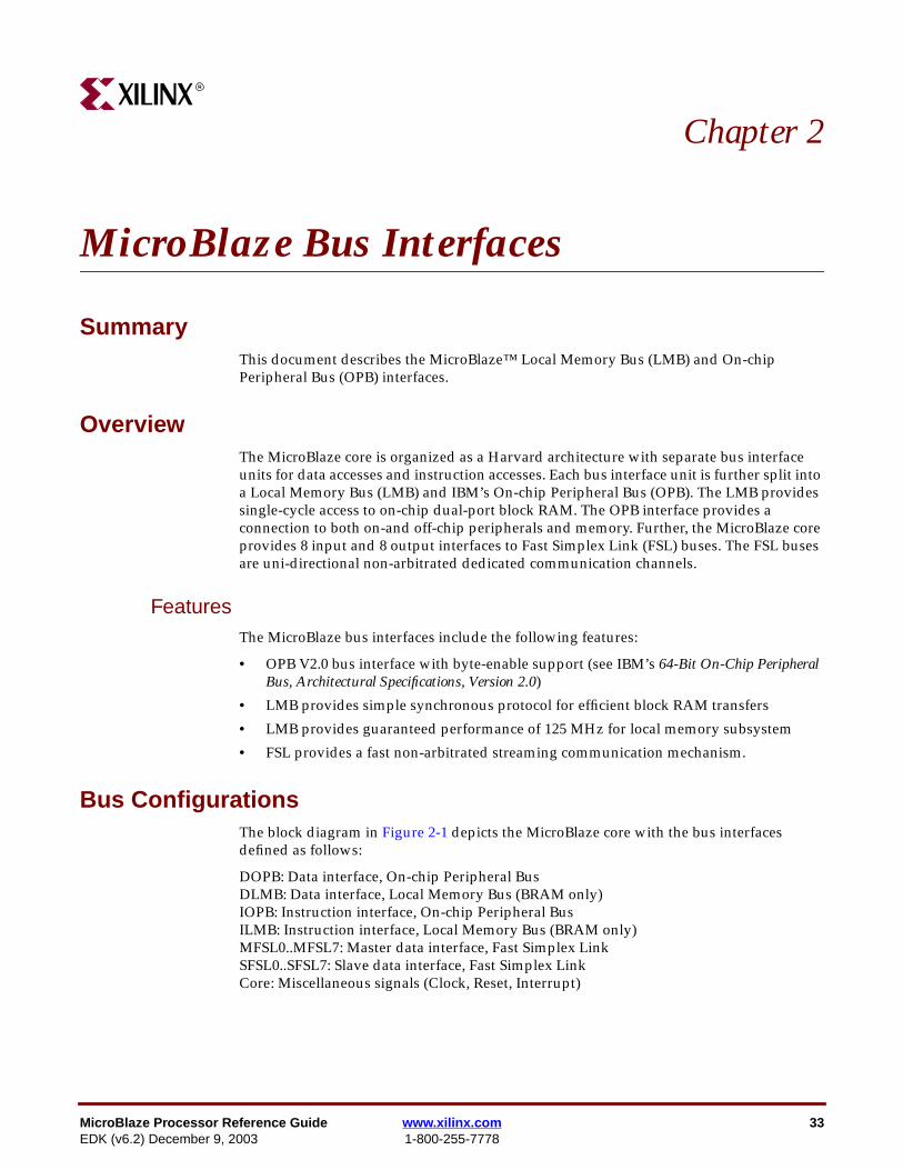
OverviewThe MicroBlaze embedded soft core is a reduced instruction set computer (RISC)optimized for implementation in Xilinx field programmable gate arrays (FPGAs). SeeFigure 1-1 for a block diagram depicting the MicroBlaze core.
FeaturesThe MicroBlaze embedded soft core includes the following features:
• Thirty-two 32-bit general purpose registers
• 32-bit instruction word with three operands and two addressing modes
• Separate 32-bit instruction and data buses that conform to IBM’s OPB (On-chipPeripheral Bus) specification
• Separate 32-bit instruction and data buses with direct connection to on-chip blockRAM through a LMB (Local Memory Bus)
• 32-bit address bus
• Single issue pipeline
• Instruction and data cache
• Hardware debug logic
• FSL (Fast Simplex Link) support
• Hardware multiplier (in Virtex-II and subsequent devices
12 www.xilinx.com MicroBlaze Processor Reference Guide1-800-255-7778 EDK (v6.2) December 9, 2003
Chapter 1: MicroBlaze ArchitectureR
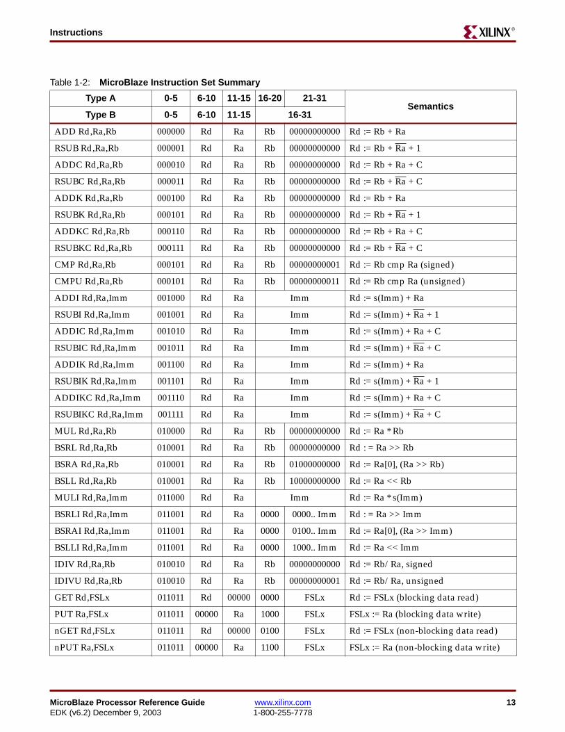
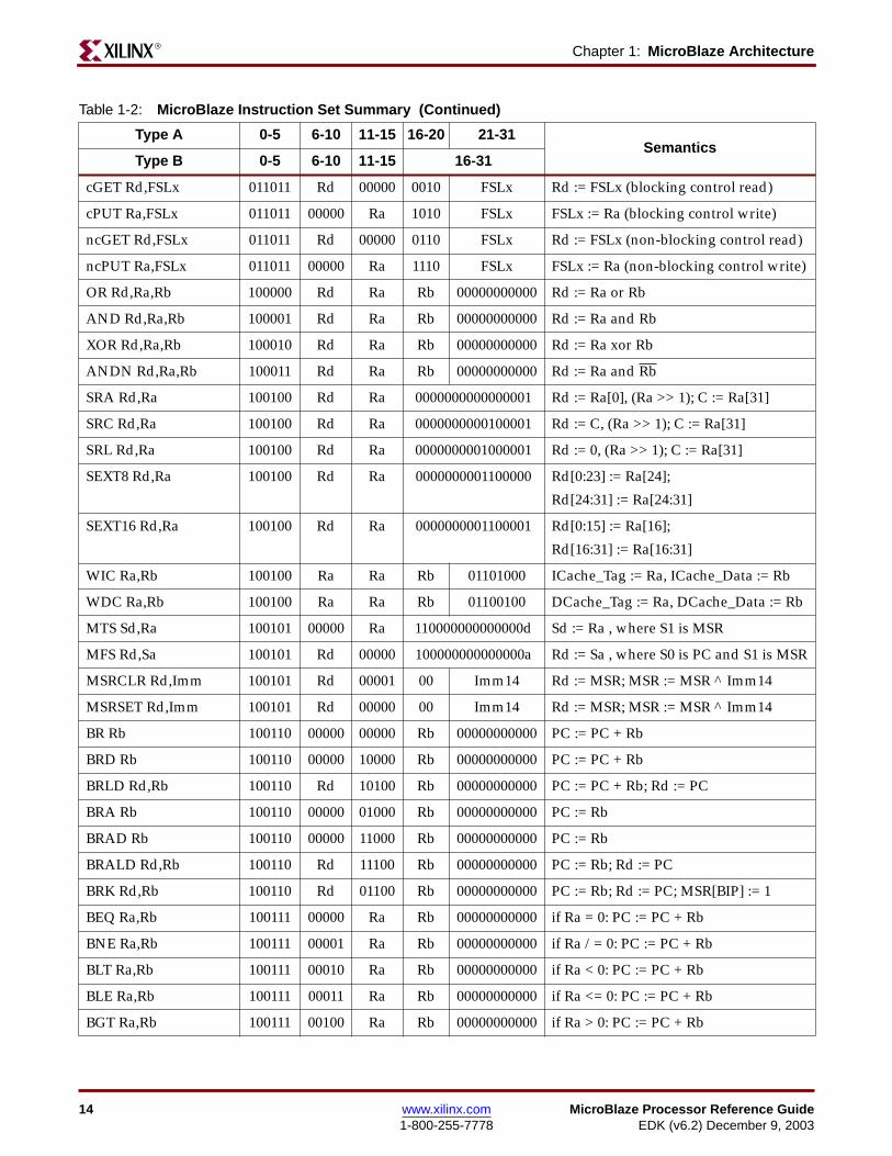
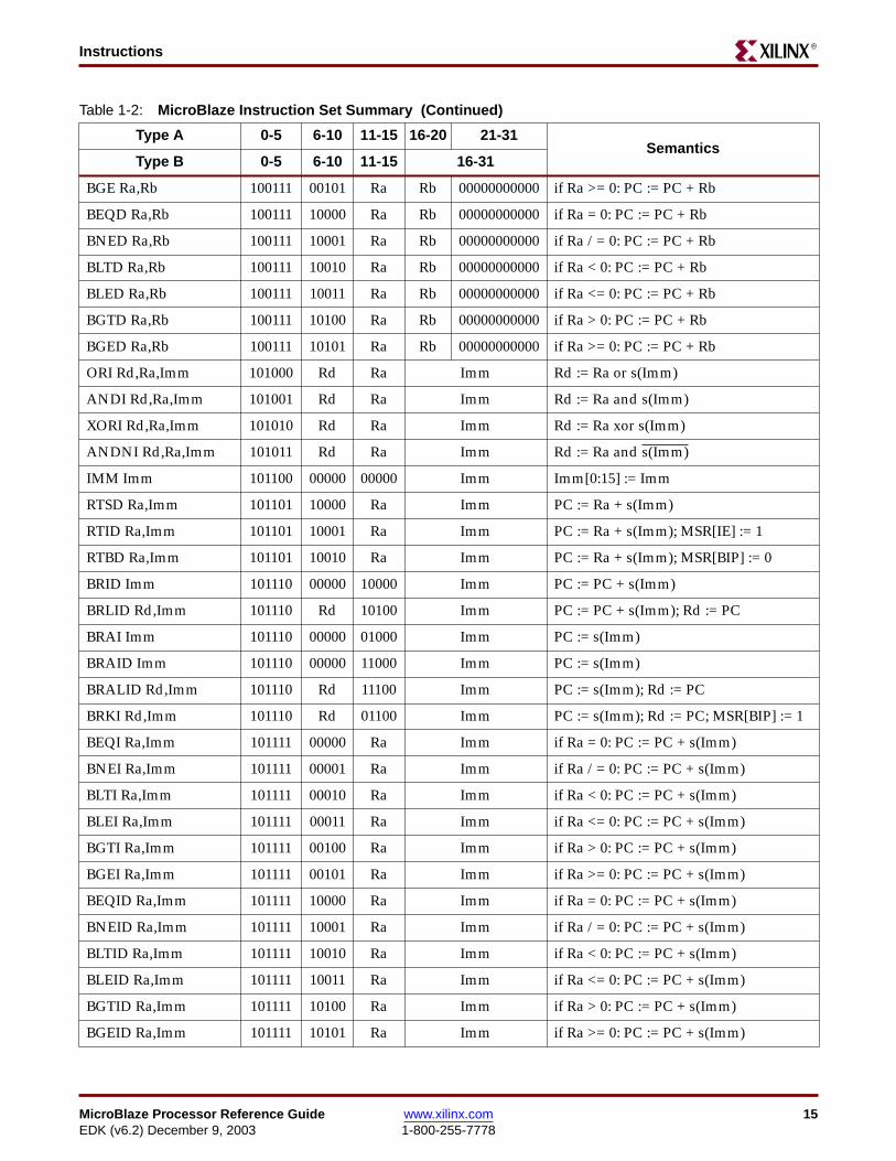
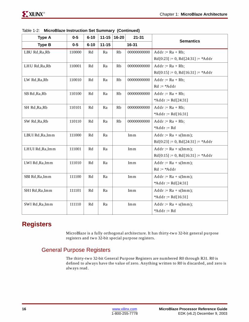
InstructionsAll MicroBlaze instructions are 32 bits and are defined as either Type A or Type B. Type Ainstructions have up to two source register operands and one destination register operand.Type B instructions have one source register and a 16-bit immediate operand (which can beextended to 32 bits by preceding the Type B instruction with an IMM instruction). Type Binstructions have a single destination register operand. Instructions are provided in thefollowing functional categories: arithmetic, logical, branch, load/store, and special.Table 1-2 lists the MicroBlaze instruction set. Refer to the MicroBlaze Instruction SetArchitecture document for more information on these instructions. Table 1-1 describes theinstruction set nomenclature used in the semantics of each instruction.
Figure 1-1: MicroBlaze Core Block Diagram
Data-sideInstruction-side
DLMB
DOPB
ILMB
IOPB
bus interface bus interface
InstructionBuffer
ProgramCounter
Register File32 X 32b
Add/Sub
Shift/Logical
Multiply
InstructionDecode
BusIF
BusIF
MFSL0..7
SFSL0..7
Table 1-1: Instruction Set Nomenclature
Symbol Description
Ra R0 - R31, General Purpose Register, source operand a
Rb R0 - R31, General Purpose Register, source operand b
Rd R0 - R31, General Purpose Register, destination operand,
C Carry flag, MSR[29]
Sa Special Purpose Register, source operand
Sd Special Purpose Register, destination operand
s(x) Sign extend argument x to 32-bit value
*Addr Memory contents at location Addr (data-size aligned)
MicroBlaze Processor Reference Guide www.xilinx.com 13EDK (v6.2) December 9, 2003 1-800-255-7778
InstructionsR
Table 1-2: MicroBlaze Instruction Set Summary
Type A 0-5 6-10 11-15 16-20 21-31Semantics
Type B 0-5 6-10 11-15 16-31
ADD Rd,Ra,Rb 000000 Rd Ra Rb 00000000000 Rd := Rb + Ra
RSUB Rd,Ra,Rb 000001 Rd Ra Rb 00000000000 Rd := Rb + Ra + 1
ADDC Rd,Ra,Rb 000010 Rd Ra Rb 00000000000 Rd := Rb + Ra + C
RSUBC Rd,Ra,Rb 000011 Rd Ra Rb 00000000000 Rd := Rb + Ra + C
ADDK Rd,Ra,Rb 000100 Rd Ra Rb 00000000000 Rd := Rb + Ra
RSUBK Rd,Ra,Rb 000101 Rd Ra Rb 00000000000 Rd := Rb + Ra + 1
ADDKC Rd,Ra,Rb 000110 Rd Ra Rb 00000000000 Rd := Rb + Ra + C
RSUBKC Rd,Ra,Rb 000111 Rd Ra Rb 00000000000 Rd := Rb + Ra + C
CMP Rd,Ra,Rb 000101 Rd Ra Rb 00000000001 Rd := Rb cmp Ra (signed)
CMPU Rd,Ra,Rb 000101 Rd Ra Rb 00000000011 Rd := Rb cmp Ra (unsigned)
ADDI Rd,Ra,Imm 001000 Rd Ra Imm Rd := s(Imm) + Ra
RSUBI Rd,Ra,Imm 001001 Rd Ra Imm Rd := s(Imm) + Ra + 1
ADDIC Rd,Ra,Imm 001010 Rd Ra Imm Rd := s(Imm) + Ra + C
RSUBIC Rd,Ra,Imm 001011 Rd Ra Imm Rd := s(Imm) + Ra + C
ADDIK Rd,Ra,Imm 001100 Rd Ra Imm Rd := s(Imm) + Ra
RSUBIK Rd,Ra,Imm 001101 Rd Ra Imm Rd := s(Imm) + Ra + 1
ADDIKC Rd,Ra,Imm 001110 Rd Ra Imm Rd := s(Imm) + Ra + C
RSUBIKC Rd,Ra,Imm 001111 Rd Ra Imm Rd := s(Imm) + Ra + C
MUL Rd,Ra,Rb 010000 Rd Ra Rb 00000000000 Rd := Ra * Rb
BSRL Rd,Ra,Rb 010001 Rd Ra Rb 00000000000 Rd : = Ra >> Rb
BSRA Rd,Ra,Rb 010001 Rd Ra Rb 01000000000 Rd := Ra[0], (Ra >> Rb)
BSLL Rd,Ra,Rb 010001 Rd Ra Rb 10000000000 Rd := Ra << Rb
MULI Rd,Ra,Imm 011000 Rd Ra Imm Rd := Ra * s(Imm)
BSRLI Rd,Ra,Imm 011001 Rd Ra 0000 0000.. Imm Rd : = Ra >> Imm
BSRAI Rd,Ra,Imm 011001 Rd Ra 0000 0100.. Imm Rd := Ra[0], (Ra >> Imm)
BSLLI Rd,Ra,Imm 011001 Rd Ra 0000 1000.. Imm Rd := Ra << Imm
IDIV Rd,Ra,Rb 010010 Rd Ra Rb 00000000000 Rd := Rb/Ra, signed
IDIVU Rd,Ra,Rb 010010 Rd Ra Rb 00000000001 Rd := Rb/Ra, unsigned
GET Rd,FSLx 011011 Rd 00000 0000 FSLx Rd := FSLx (blocking data read)
PUT Ra,FSLx 011011 00000 Ra 1000 FSLx FSLx := Ra (blocking data write)
nGET Rd,FSLx 011011 Rd 00000 0100 FSLx Rd := FSLx (non-blocking data read)
nPUT Ra,FSLx 011011 00000 Ra 1100 FSLx FSLx := Ra (non-blocking data write)
14 www.xilinx.com MicroBlaze Processor Reference Guide1-800-255-7778 EDK (v6.2) December 9, 2003
Chapter 1: MicroBlaze ArchitectureR
cGET Rd,FSLx 011011 Rd 00000 0010 FSLx Rd := FSLx (blocking control read)
cPUT Ra,FSLx 011011 00000 Ra 1010 FSLx FSLx := Ra (blocking control write)
ncGET Rd,FSLx 011011 Rd 00000 0110 FSLx Rd := FSLx (non-blocking control read)
ncPUT Ra,FSLx 011011 00000 Ra 1110 FSLx FSLx := Ra (non-blocking control write)
OR Rd,Ra,Rb 100000 Rd Ra Rb 00000000000 Rd := Ra or Rb
AND Rd,Ra,Rb 100001 Rd Ra Rb 00000000000 Rd := Ra and Rb
XOR Rd,Ra,Rb 100010 Rd Ra Rb 00000000000 Rd := Ra xor Rb
ANDN Rd,Ra,Rb 100011 Rd Ra Rb 00000000000 Rd := Ra and Rb
SRA Rd,Ra 100100 Rd Ra 0000000000000001 Rd := Ra[0], (Ra >> 1); C := Ra[31]
SRC Rd,Ra 100100 Rd Ra 0000000000100001 Rd := C, (Ra >> 1); C := Ra[31]
SRL Rd,Ra 100100 Rd Ra 0000000001000001 Rd := 0, (Ra >> 1); C := Ra[31]
SEXT8 Rd,Ra 100100 Rd Ra 0000000001100000 Rd[0:23] := Ra[24];
Rd[24:31] := Ra[24:31]
SEXT16 Rd,Ra 100100 Rd Ra 0000000001100001 Rd[0:15] := Ra[16];
Rd[16:31] := Ra[16:31]
WIC Ra,Rb 100100 Ra Ra Rb 01101000 ICache_Tag := Ra, ICache_Data := Rb
WDC Ra,Rb 100100 Ra Ra Rb 01100100 DCache_Tag := Ra, DCache_Data := Rb
MTS Sd,Ra 100101 00000 Ra 110000000000000d Sd := Ra , where S1 is MSR
MFS Rd,Sa 100101 Rd 00000 100000000000000a Rd := Sa , where S0 is PC and S1 is MSR
MSRCLR Rd,Imm 100101 Rd 00001 00 Imm14 Rd := MSR; MSR := MSR ^ Imm14
MSRSET Rd,Imm 100101 Rd 00000 00 Imm14 Rd := MSR; MSR := MSR ^ Imm14
BR Rb 100110 00000 00000 Rb 00000000000 PC := PC + Rb
BRD Rb 100110 00000 10000 Rb 00000000000 PC := PC + Rb
BRLD Rd,Rb 100110 Rd 10100 Rb 00000000000 PC := PC + Rb; Rd := PC
BRA Rb 100110 00000 01000 Rb 00000000000 PC := Rb
BRAD Rb 100110 00000 11000 Rb 00000000000 PC := Rb
BRALD Rd,Rb 100110 Rd 11100 Rb 00000000000 PC := Rb; Rd := PC
BRK Rd,Rb 100110 Rd 01100 Rb 00000000000 PC := Rb; Rd := PC; MSR[BIP] := 1
BEQ Ra,Rb 100111 00000 Ra Rb 00000000000 if Ra = 0: PC := PC + Rb
BNE Ra,Rb 100111 00001 Ra Rb 00000000000 if Ra /= 0: PC := PC + Rb
BLT Ra,Rb 100111 00010 Ra Rb 00000000000 if Ra < 0: PC := PC + Rb
BLE Ra,Rb 100111 00011 Ra Rb 00000000000 if Ra <= 0: PC := PC + Rb
BGT Ra,Rb 100111 00100 Ra Rb 00000000000 if Ra > 0: PC := PC + Rb
Table 1-2: MicroBlaze Instruction Set Summary (Continued)
Type A 0-5 6-10 11-15 16-20 21-31Semantics
Type B 0-5 6-10 11-15 16-31
MicroBlaze Processor Reference Guide www.xilinx.com 15EDK (v6.2) December 9, 2003 1-800-255-7778
InstructionsR
BGE Ra,Rb 100111 00101 Ra Rb 00000000000 if Ra >= 0: PC := PC + Rb
BEQD Ra,Rb 100111 10000 Ra Rb 00000000000 if Ra = 0: PC := PC + Rb
BNED Ra,Rb 100111 10001 Ra Rb 00000000000 if Ra /= 0: PC := PC + Rb
BLTD Ra,Rb 100111 10010 Ra Rb 00000000000 if Ra < 0: PC := PC + Rb
BLED Ra,Rb 100111 10011 Ra Rb 00000000000 if Ra <= 0: PC := PC + Rb
BGTD Ra,Rb 100111 10100 Ra Rb 00000000000 if Ra > 0: PC := PC + Rb
BGED Ra,Rb 100111 10101 Ra Rb 00000000000 if Ra >= 0: PC := PC + Rb
ORI Rd,Ra,Imm 101000 Rd Ra Imm Rd := Ra or s(Imm)
ANDI Rd,Ra,Imm 101001 Rd Ra Imm Rd := Ra and s(Imm)
XORI Rd,Ra,Imm 101010 Rd Ra Imm Rd := Ra xor s(Imm)
ANDNI Rd,Ra,Imm 101011 Rd Ra Imm Rd := Ra and s(Imm)
IMM Imm 101100 00000 00000 Imm Imm[0:15] := Imm
RTSD Ra,Imm 101101 10000 Ra Imm PC := Ra + s(Imm)
RTID Ra,Imm 101101 10001 Ra Imm PC := Ra + s(Imm); MSR[IE] := 1
RTBD Ra,Imm 101101 10010 Ra Imm PC := Ra + s(Imm); MSR[BIP] := 0
BRID Imm 101110 00000 10000 Imm PC := PC + s(Imm)
BRLID Rd,Imm 101110 Rd 10100 Imm PC := PC + s(Imm); Rd := PC
BRAI Imm 101110 00000 01000 Imm PC := s(Imm)
BRAID Imm 101110 00000 11000 Imm PC := s(Imm)
BRALID Rd,Imm 101110 Rd 11100 Imm PC := s(Imm); Rd := PC
BRKI Rd,Imm 101110 Rd 01100 Imm PC := s(Imm); Rd := PC; MSR[BIP] := 1
BEQI Ra,Imm 101111 00000 Ra Imm if Ra = 0: PC := PC + s(Imm)
BNEI Ra,Imm 101111 00001 Ra Imm if Ra /= 0: PC := PC + s(Imm)
BLTI Ra,Imm 101111 00010 Ra Imm if Ra < 0: PC := PC + s(Imm)
BLEI Ra,Imm 101111 00011 Ra Imm if Ra <= 0: PC := PC + s(Imm)
BGTI Ra,Imm 101111 00100 Ra Imm if Ra > 0: PC := PC + s(Imm)
BGEI Ra,Imm 101111 00101 Ra Imm if Ra >= 0: PC := PC + s(Imm)
BEQID Ra,Imm 101111 10000 Ra Imm if Ra = 0: PC := PC + s(Imm)
BNEID Ra,Imm 101111 10001 Ra Imm if Ra /= 0: PC := PC + s(Imm)
BLTID Ra,Imm 101111 10010 Ra Imm if Ra < 0: PC := PC + s(Imm)
BLEID Ra,Imm 101111 10011 Ra Imm if Ra <= 0: PC := PC + s(Imm)
BGTID Ra,Imm 101111 10100 Ra Imm if Ra > 0: PC := PC + s(Imm)
BGEID Ra,Imm 101111 10101 Ra Imm if Ra >= 0: PC := PC + s(Imm)
Table 1-2: MicroBlaze Instruction Set Summary (Continued)
Type A 0-5 6-10 11-15 16-20 21-31Semantics
Type B 0-5 6-10 11-15 16-31
16 www.xilinx.com MicroBlaze Processor Reference Guide1-800-255-7778 EDK (v6.2) December 9, 2003
Chapter 1: MicroBlaze ArchitectureR
RegistersMicroBlaze is a fully orthogonal architecture. It has thirty-two 32-bit general purposeregisters and two 32-bit special purpose registers.
General Purpose RegistersThe thirty-two 32-bit General Purpose Registers are numbered R0 through R31. R0 isdefined to always have the value of zero. Anything written to R0 is discarded, and zero isalways read.
LBU Rd,Ra,Rb 110000 Rd Ra Rb 00000000000 Addr := Ra + Rb;
Rd[0:23] := 0, Rd[24:31] := *Addr
LHU Rd,Ra,Rb 110001 Rd Ra Rb 00000000000 Addr := Ra + Rb;
Rd[0:15] := 0, Rd[16:31] := *Addr
LW Rd,Ra,Rb 110010 Rd Ra Rb 00000000000 Addr := Ra + Rb;
Rd := *Addr
SB Rd,Ra,Rb 110100 Rd Ra Rb 00000000000 Addr := Ra + Rb;
*Addr := Rd[24:31]
SH Rd,Ra,Rb 110101 Rd Ra Rb 00000000000 Addr := Ra + Rb;
*Addr := Rd[16:31]
SW Rd,Ra,Rb 110110 Rd Ra Rb 00000000000 Addr := Ra + Rb;
*Addr := Rd
LBUI Rd,Ra,Imm 111000 Rd Ra Imm Addr := Ra + s(Imm);
Rd[0:23] := 0, Rd[24:31] := *Addr
LHUI Rd,Ra,Imm 111001 Rd Ra Imm Addr := Ra + s(Imm);
Rd[0:15] := 0, Rd[16:31] := *Addr
LWI Rd,Ra,Imm 111010 Rd Ra Imm Addr := Ra + s(Imm);
Rd := *Addr
SBI Rd,Ra,Imm 111100 Rd Ra Imm Addr := Ra + s(Imm);
*Addr := Rd[24:31]
SHI Rd,Ra,Imm 111101 Rd Ra Imm Addr := Ra + s(Imm);
*Addr := Rd[16:31]
SWI Rd,Ra,Imm 111110 Rd Ra Imm Addr := Ra + s(Imm);
*Addr := Rd
Table 1-2: MicroBlaze Instruction Set Summary (Continued)
Type A 0-5 6-10 11-15 16-20 21-31Semantics
Type B 0-5 6-10 11-15 16-31
MicroBlaze Processor Reference Guide www.xilinx.com 17EDK (v6.2) December 9, 2003 1-800-255-7778
RegistersR
Special Purpose Registers
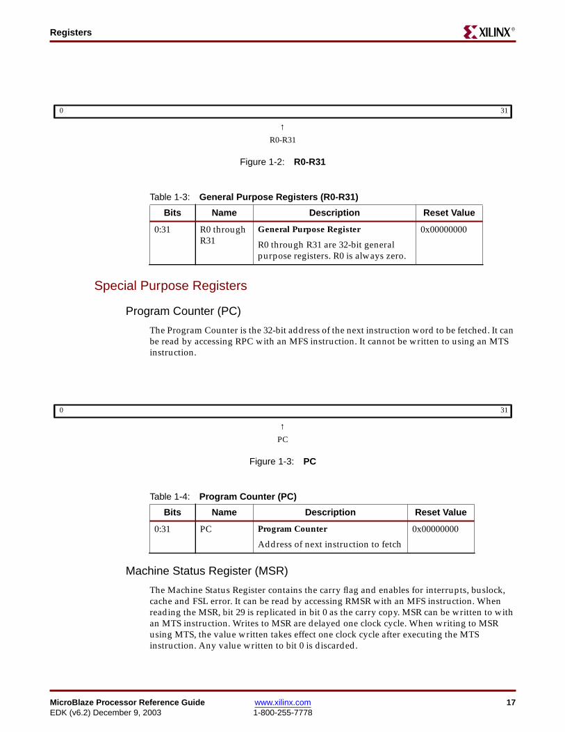
Program Counter (PC)
The Program Counter is the 32-bit address of the next instruction word to be fetched. It canbe read by accessing RPC with an MFS instruction. It cannot be written to using an MTSinstruction.
Machine Status Register (MSR)
The Machine Status Register contains the carry flag and enables for interrupts, buslock,cache and FSL error. It can be read by accessing RMSR with an MFS instruction. Whenreading the MSR, bit 29 is replicated in bit 0 as the carry copy. MSR can be written to withan MTS instruction. Writes to MSR are delayed one clock cycle. When writing to MSRusing MTS, the value written takes effect one clock cycle after executing the MTSinstruction. Any value written to bit 0 is discarded.
0 31
↑R0-R31
Figure 1-2: R0-R31
Table 1-3: General Purpose Registers (R0-R31)
Bits Name Description Reset Value
0:31 R0 throughR31
General Purpose Register
R0 through R31 are 32-bit generalpurpose registers. R0 is always zero.
0x00000000
0 31
↑PC
Figure 1-3: PC
Table 1-4: Program Counter (PC)
Bits Name Description Reset Value
0:31 PC Program Counter
Address of next instruction to fetch
0x00000000
18 www.xilinx.com MicroBlaze Processor Reference Guide1-800-255-7778 EDK (v6.2) December 9, 2003
Chapter 1: MicroBlaze ArchitectureR
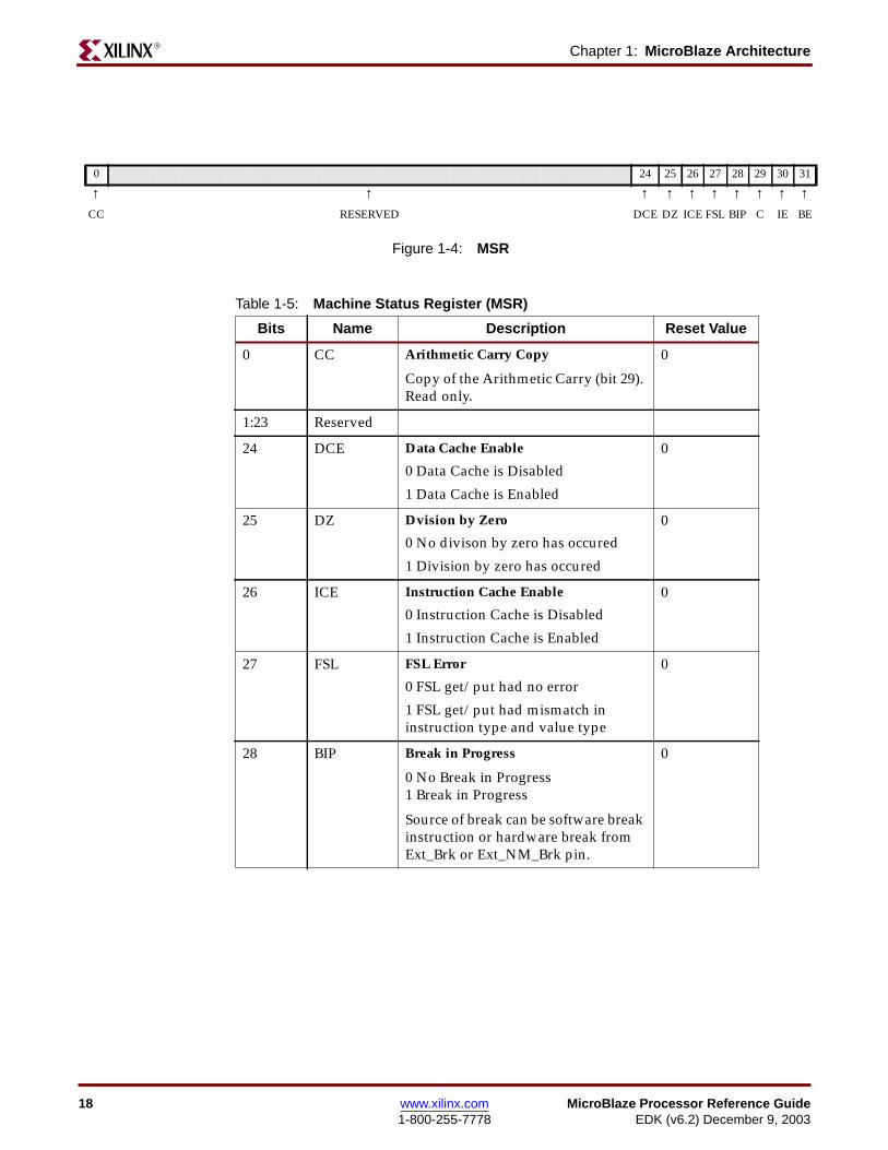
0 24 25 26 27 28 29 30 31
↑ ↑ ↑ ↑ ↑ ↑ ↑ ↑ ↑ ↑CC RESERVED DCE DZ ICE FSL BIP C IE BE
Figure 1-4: MSR
Table 1-5: Machine Status Register (MSR)
Bits Name Description Reset Value
0 CC Arithmetic Carry Copy
Copy of the Arithmetic Carry (bit 29).Read only.
0
1:23 Reserved
24 DCE Data Cache Enable
0 Data Cache is Disabled
1 Data Cache is Enabled
0
25 DZ Dvision by Zero
0 No divison by zero has occured
1 Division by zero has occured
0
26 ICE Instruction Cache Enable
0 Instruction Cache is Disabled
1 Instruction Cache is Enabled
0
27 FSL FSL Error
0 FSL get/put had no error
1 FSL get/put had mismatch ininstruction type and value type
0
28 BIP Break in Progress
0 No Break in Progress1 Break in Progress
Source of break can be software breakinstruction or hardware break fromExt_Brk or Ext_NM_Brk pin.
0
MicroBlaze Processor Reference Guide www.xilinx.com 19EDK (v6.2) December 9, 2003 1-800-255-7778
PipelineR
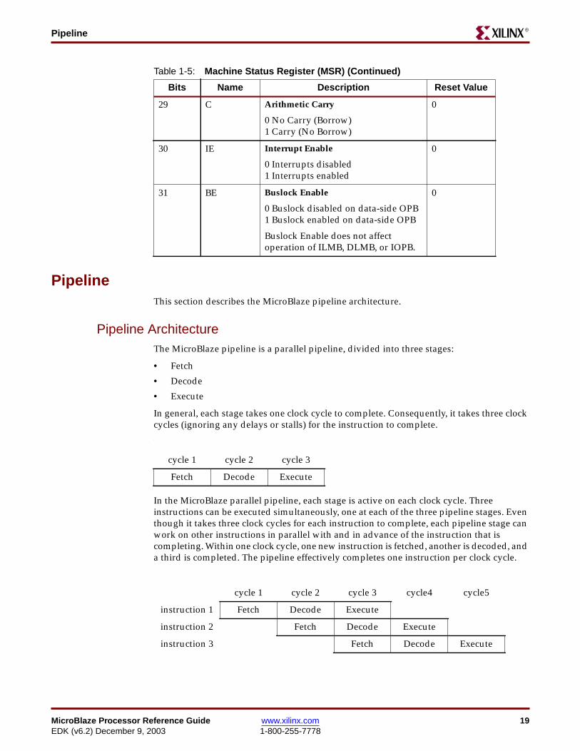
PipelineThis section describes the MicroBlaze pipeline architecture.
Pipeline ArchitectureThe MicroBlaze pipeline is a parallel pipeline, divided into three stages:
• Fetch
• Decode
• Execute
In general, each stage takes one clock cycle to complete. Consequently, it takes three clockcycles (ignoring any delays or stalls) for the instruction to complete..
In the MicroBlaze parallel pipeline, each stage is active on each clock cycle. Threeinstructions can be executed simultaneously, one at each of the three pipeline stages. Eventhough it takes three clock cycles for each instruction to complete, each pipeline stage canwork on other instructions in parallel with and in advance of the instruction that iscompleting. Within one clock cycle, one new instruction is fetched, another is decoded, anda third is completed. The pipeline effectively completes one instruction per clock cycle.
29 C Arithmetic Carry
0 No Carry (Borrow)1 Carry (No Borrow)
0
30 IE Interrupt Enable
0 Interrupts disabled1 Interrupts enabled
0
31 BE Buslock Enable
0 Buslock disabled on data-side OPB1 Buslock enabled on data-side OPB
Buslock Enable does not affectoperation of ILMB, DLMB, or IOPB.
0
Table 1-5: Machine Status Register (MSR) (Continued)
Bits Name Description Reset Value
cycle 1 cycle 2 cycle 3
Fetch Decode Execute
cycle 1 cycle 2 cycle 3 cycle4 cycle5
instruction 1 Fetch Decode Execute
instruction 2 Fetch Decode Execute
instruction 3 Fetch Decode Execute
20 www.xilinx.com MicroBlaze Processor Reference Guide1-800-255-7778 EDK (v6.2) December 9, 2003
Chapter 1: MicroBlaze ArchitectureR
BranchesSimilar to other processor pipelines, the MicroBlaze pipeline can originate control hazardsthat affect the pipeline execution rate. When an instruction that changes the control flow ofa program (branches) is executed and completed, and eventually changes the programflow (taken branches), the previous pipeline work becomes useless. When the processorexecutes a taken branch, the instructions in the fetch and decode stages are not the correctones, and must be discarded or flushed from the pipeline. The processor must refill thepipeline with the correct instructions, taking three clock cycles for a taken branch, addinga latency of two cycles for refilling the pipeline.
MicroBlaze uses two techniques to reduce the penalty of taken branches. One technique isto use delay slots and another is use of a history buffer.
Delay Slots
When the processor executes a taken branch and flushes the pipeline, it takes three clockcycles to refill the pipeline. By allowing the instruction following a branch to complete, thispenalty is reduced. Instead of flushing the instructions in both the fetch and decode stages,only the fetch stage is discarded and the instruction in the decode stage is allowed tocomplete. This effectively produces a delayed branch or delay slot. Since the work done onthe delay slot instruction is not discarded, this technique effectively reduces the branchpenalty from two clock cycles to one. Branch instructions that allow execution of thesubsequent instruction in the delay slot are denoted by a D in the instruction mnemonic.For example, the BNE instruction does not execute the subsequent instruction in the delayslot, whereas BNED does execute the next instruction in the delay slot before control istransferred to the branch location.
Load/Store ArchitectureMicroBlaze can access memory in the following three data sizes:
• Byte (8 bits)
• Halfword (16 bits)
• Word (32 bits)
Memory accesses are always data-size aligned. For halfword accesses, the least significantaddress bit is forced to 0. Similarly, for word accesses, the two least significant address bitsare forced to 0.
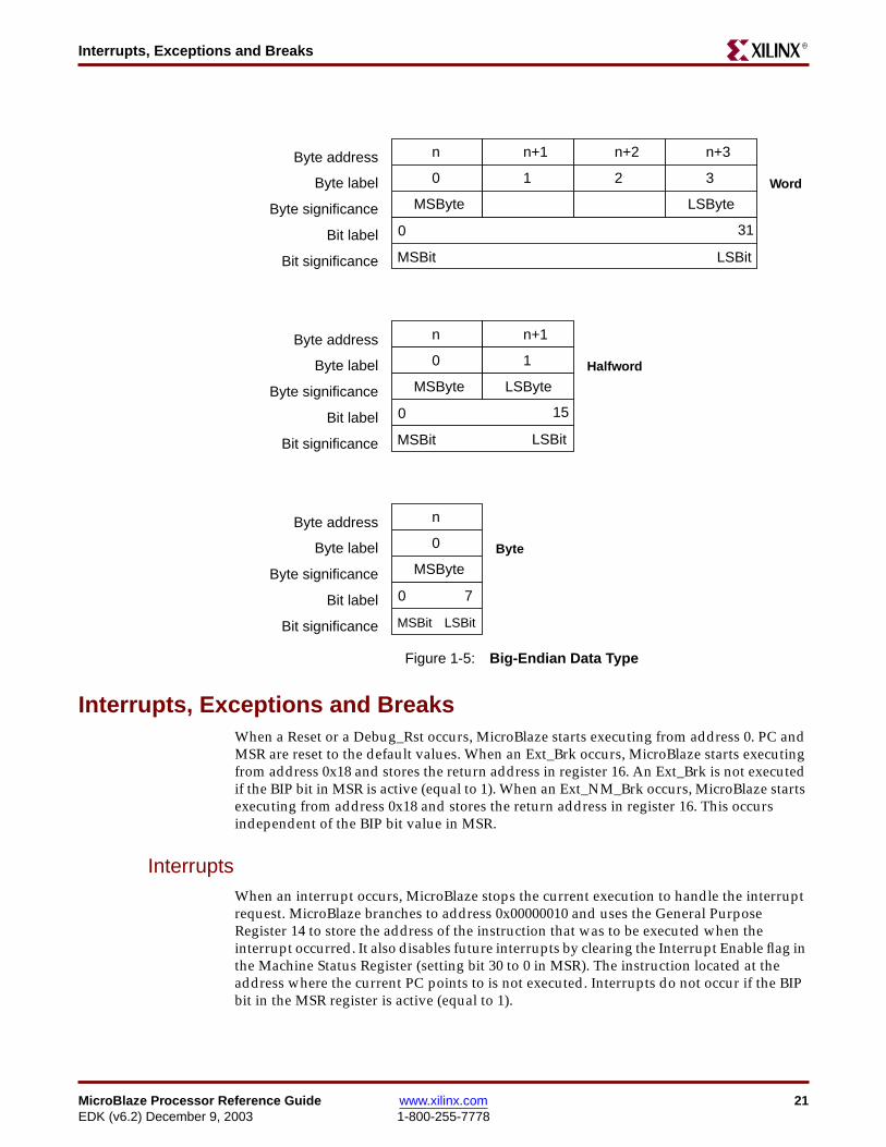
MicroBlaze is a Big-Endian processor and uses the Big-Endian address and labelingconventions shown in Figure 1-5 when accessing memory. The following abbreviations areused:
• MSByte: Most Significant Byte
• LSByte: Least Significant Byte
• MSBit: Most Significant Bit
• LSBit: Least Significant Bit
MicroBlaze Processor Reference Guide www.xilinx.com 21EDK (v6.2) December 9, 2003 1-800-255-7778
Interrupts, Exceptions and BreaksR
Interrupts, Exceptions and BreaksWhen a Reset or a Debug_Rst occurs, MicroBlaze starts executing from address 0. PC andMSR are reset to the default values. When an Ext_Brk occurs, MicroBlaze starts executingfrom address 0x18 and stores the return address in register 16. An Ext_Brk is not executedif the BIP bit in MSR is active (equal to 1). When an Ext_NM_Brk occurs, MicroBlaze startsexecuting from address 0x18 and stores the return address in register 16. This occursindependent of the BIP bit value in MSR.
InterruptsWhen an interrupt occurs, MicroBlaze stops the current execution to handle the interruptrequest. MicroBlaze branches to address 0x00000010 and uses the General PurposeRegister 14 to store the address of the instruction that was to be executed when theinterrupt occurred. It also disables future interrupts by clearing the Interrupt Enable flag inthe Machine Status Register (setting bit 30 to 0 in MSR). The instruction located at theaddress where the current PC points to is not executed. Interrupts do not occur if the BIPbit in the MSR register is active (equal to 1).
Figure 1-5: Big-Endian Data Type
n n+1 n+2 n+3
0 1 2 3
MSByte LSByte
0 31
MSBit LSBit
Byte address
Byte label
Byte significance
Bit label
Bit significance
n n+1
0 1
MSByte LSByte
0 15
MSBit LSBit
Byte address
Byte label
Byte significance
Bit label
Bit significance
n
0
MSByte
0 7
MSBit LSBit
Byte address
Byte label
Byte significance
Bit label
Bit significance
Byte
Halfword
Word
22 www.xilinx.com MicroBlaze Processor Reference Guide1-800-255-7778 EDK (v6.2) December 9, 2003
Chapter 1: MicroBlaze ArchitectureR
Latency
The time it will take MicroBlaze to enter an Interrupt Service Routine (ISR) from the timean interrupt occurs, depends on the configuration of the processor. If MicroBlaze isconfiguredto have a hardware divider, the largest latency will happen when an interruptoccurs during the execuion of a division instruction.
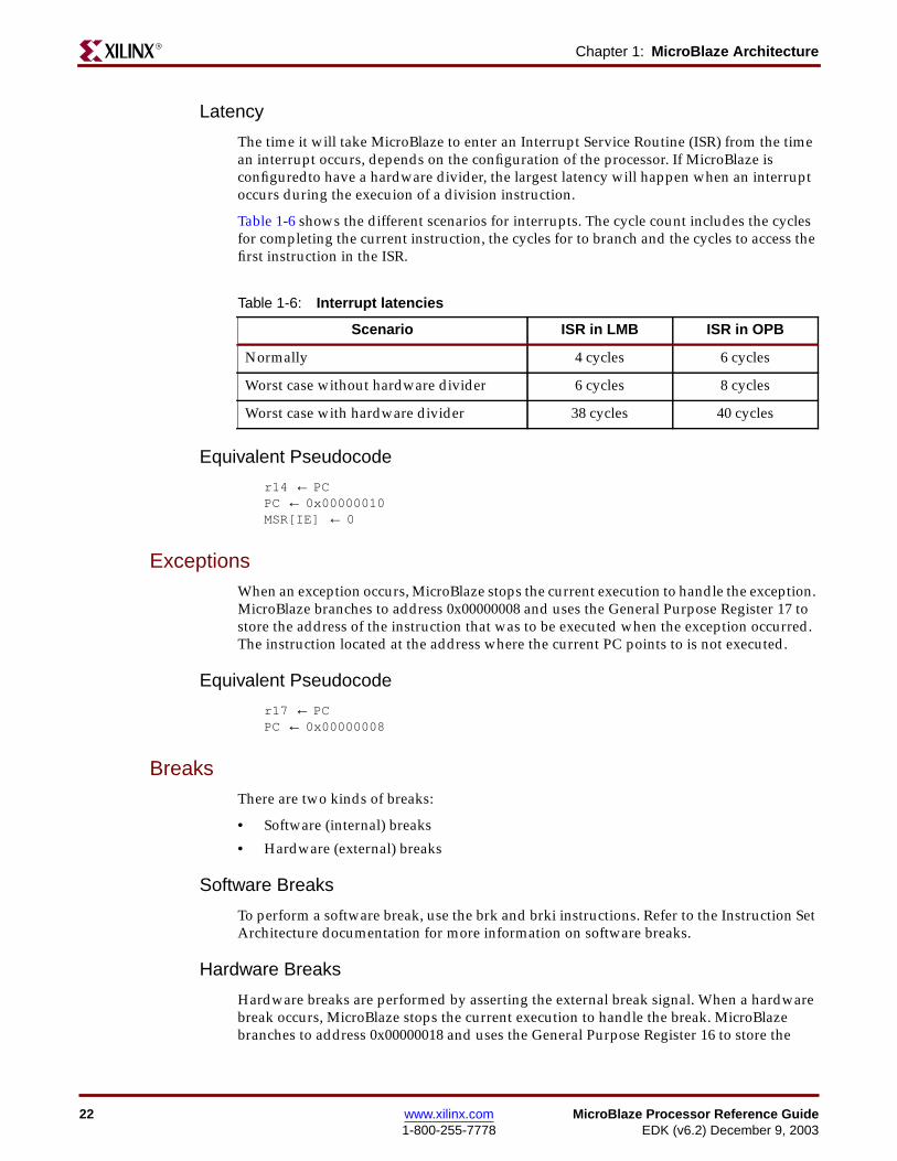
Table 1-6 shows the different scenarios for interrupts. The cycle count includes the cyclesfor completing the current instruction, the cycles for to branch and the cycles to access thefirst instruction in the ISR.
Equivalent Pseudocode
r14 ← PCPC ← 0x00000010MSR[IE] ← 0
ExceptionsWhen an exception occurs, MicroBlaze stops the current execution to handle the exception.MicroBlaze branches to address 0x00000008 and uses the General Purpose Register 17 tostore the address of the instruction that was to be executed when the exception occurred.The instruction located at the address where the current PC points to is not executed.
Equivalent Pseudocode
r17 ← PCPC ← 0x00000008
BreaksThere are two kinds of breaks:
• Software (internal) breaks
• Hardware (external) breaks
Software Breaks
To perform a software break, use the brk and brki instructions. Refer to the Instruction SetArchitecture documentation for more information on software breaks.
Hardware Breaks
Hardware breaks are performed by asserting the external break signal. When a hardwarebreak occurs, MicroBlaze stops the current execution to handle the break. MicroBlazebranches to address 0x00000018 and uses the General Purpose Register 16 to store the
Table 1-6: Interrupt latencies
Scenario ISR in LMB ISR in OPB
Normally 4 cycles 6 cycles
Worst case without hardware divider 6 cycles 8 cycles
Worst case with hardware divider 38 cycles 40 cycles
MicroBlaze Processor Reference Guide www.xilinx.com 23EDK (v6.2) December 9, 2003 1-800-255-7778
Instruction CacheR
address of the instruction that was to be executed when the break occurred. MicroBlazealso disables future breaks by setting the Break In Progress (BIP) flag in the Machine StatusRegister (setting bit 28 to 1 in MSR). The instruction located at the address where thecurrent PC points to is not executed.
Hardware breaks are only handled when there is no break in progress (the Break InProgress flag is set to 0). The Break In Progress flag has higher precedence than theInterrupt Enabled flag. While no interrupts are handled when the Break In Progress flag isset, breaks that occur when interrupts are disabled are handled immediately. However, it isimportant to note that non-maskable hardware breaks are always handled immediately.
Equivalent Pseudocode
r16 ← PCPC ← 0x00000018MSR[BIP] ← 1
Instruction Cache
OverviewMicroBlaze may be used with an optional instruction cache for improved performancewhen executing code that resides outside the LMB address range.
The instruction cache has the following features
• User selectable cacheable memory area
• Configurable cache size and tag size
• Individual cache line lock capability
• Cache on and off controlled using a new bit in the MSR register
• Instructions to write to the instruction cache
• Does not require special memory controllers. Will work with existing OPB peripherals
• Memory is organized into a cacheable and a non-cacheable segment
• Very little area or frequency impact ( < 20 LUTs)
• Can be used in conjunction with Instruction side LMB
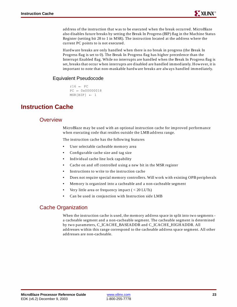
Cache OrganizationWhen the instruction cache is used, the memory address space in split into two segments -a cacheable segment and a non-cacheable segment. The cacheable segment is determinedby two parameters, C_ICACHE_BASEADDR and C_ICACHE_HIGHADDR. Alladdresses within this range correspond to the cacheable address space segment. All otheraddresses are non-cacheable.
24 www.xilinx.com MicroBlaze Processor Reference Guide1-800-255-7778 EDK (v6.2) December 9, 2003
Chapter 1: MicroBlaze ArchitectureR
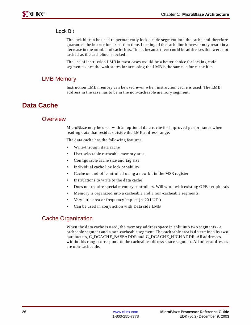
All cacheable instruction addresses are further split into two segments - a cache linesegment and a tag address segment. The size of the two segments can be configured by theuser. The address bits between bit 0 and the first tag address bit are ignored in the cache.The size of the cache line can be between 9 to 14 bits. This results in a cache sizes rangingfrom 4 Kbytes to 64 Kbytes. There is no limit on the tag address size.
Cache OperationIn the instruction fetch stage, MicroBlaze writes the instruction address to the instructionaddress bus and waits for a ready signal. To reduce wait states, a request is donesimultaneously on the instruction OPB and the instruction LMB. If an acknowledge signalis received from the LMB in the next cycle, the instruction access from OPB is aborted. Forevery instruction fetched, the instruction cache detects if the instruction address belongs tothe cacheable segment. If the address is non-cacheable, the cache ignores the instructionand allows the LMB or the OPB to fulfill the request. If the address is cacheable, a lookupis performed on the tag memory to check if the requested instruction is in the cache. Thelookup is successful when both the valid bit is set and the tag address is the same as the tagaddress segment of the instruction address.
Figure 1-6: Cache Organization
Instruction Address Bits0 30 31
Cache LineTag Address --
Tag
Instruction BRAM
BRAMAddr
Addr
=Tag
ValidCache_Hit
Cache_instruction_data
MicroBlaze Processor Reference Guide www.xilinx.com 25EDK (v6.2) December 9, 2003 1-800-255-7778
Instruction CacheR
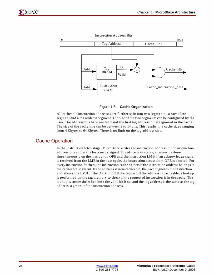
If the instruction is in the cache, the cache will drive the ready signal (Cache_Hit) forMicroBlaze and the instruction data for the address. If the instruction is not in the cache,the cache will not drive the ready signal but will wait until the OPB fulfills the request andupdates the cache with the new information.
Software
MSR Bit
Bit 26 in the MSR indicates whether or not the cache is enabled. The MFS and MTSinstructions are used to read and write to the MSR respectively.
The contents of the cache are preserved by default when the cache is disabled. The usermay overwrite the contents of the cache using the WIC instruction or using the hardwaredebug logic of MicroBlaze.
WIC Instruction
The WIC instruction may be used to update the instruction cache from a softwareprogram. The assembly instruction is
WIC Ra,Rb
Where Ra contains cache line, tag address, valid and lock bit, Rb contains the instructiondata.
Ra(31) is the lock bit, Ra(30) is the valid bit (valid when bit is set to ‘1’), the rest of the Racontains the instruction address.
This instruction can only be used when the cache is disabled. The lock bit is described inthe Lock Bit section below. The
HW Debug Logic
The HW debug logic may be used to perform a similar operation as the WIC instruction.
Figure 1-7: Cache Operation
IOPB_Address
IOPB_Data
Cache Line
Tag Address
0,1 (Locked,Valid)
Instruction BRAM
Tag BRAM
Data
Data
Address
Address
WE
WE
IOPB_XferAck
0 1
IOPB_Select
26 www.xilinx.com MicroBlaze Processor Reference Guide1-800-255-7778 EDK (v6.2) December 9, 2003
Chapter 1: MicroBlaze ArchitectureR
Lock Bit
The lock bit can be used to permanently lock a code segment into the cache and thereforeguarantee the instruction execution time. Locking of the cacheline however may result in adecrease in the number of cache hits. This is because there could be addresses that were notcached as the cacheline is locked.
The use of instruction LMB in most cases would be a better choice for locking codesegments since the wait states for accessing the LMB is the same as for cache hits.
LMB MemoryInstruction LMB memory can be used even when instruction cache is used. The LMBaddress in the case has to be in the non-cacheable memory segment.
Data Cache
OverviewMicroBlaze may be used with an optional data cache for improved performance whenreading data that resides outside the LMB address range.
The data cache has the following features
• Write-through data cache
• User selectable cacheable memory area
• Configurable cache size and tag size
• Individual cache line lock capability
• Cache on and off controlled using a new bit in the MSR register
• Instructions to write to the data cache
• Does not require special memory controllers. Will work with existing OPB peripherals
• Memory is organized into a cacheable and a non-cacheable segments
• Very little area or frequency impact ( < 20 LUTs)
• Can be used in conjunction with Data side LMB
Cache OrganizationWhen the data cache is used, the memory address space in split into two segments - acacheable segment and a non-cacheable segment. The cacheable area is determined by twoparameters, C_DCACHE_BASEADDR and C_DCACHE_HIGHADDR. All addresseswithin this range correspond to the cacheable address space segment. All other addressesare non-cacheable.
MicroBlaze Processor Reference Guide www.xilinx.com 27EDK (v6.2) December 9, 2003 1-800-255-7778
Data CacheR
All cacheable data addresses are further split into two segments - a cache line segment anda tag address segment. The size of the two segments can be configured by the user. Theaddress bits between bit 0 and the first tag address bit are ignored in the cache. The size ofthe cache line can be between 9 to 14 bits. This results in a cache sizes ranging from 4Kbytes to 64 Kbytes. There is no limit on the tag address size.
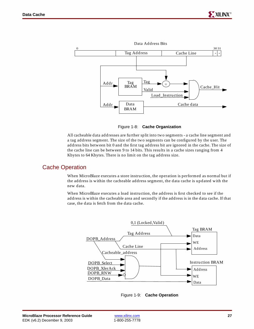
Cache OperationWhen MicroBlaze executes a store instruction, the operation is performed as normal but ifthe address is within the cacheable address segment, the data cache is updated with thenew data.
When MicroBlaze executes a load instruction, the address is first checked to see if theaddress is within the cacheable area and secondly if the address is in the data cache. If thatcase, the data is fetch from the data cache.
Figure 1-8: Cache Organization
Data Address Bits0 30 31
Cache LineTag Address --
Tag
Data BRAM
BRAMAddr
Addr
=Tag
ValidCache_Hit
Cache data
Load_Instruction
Figure 1-9: Cache Operation
DOPB_Address
DOPB_Data
Cache Line
Tag Address
0,1 (Locked,Valid)
Instruction BRAM
Tag BRAM
Data
Data
Address
Address
WE
WE
DOPB_XferAckDOPB_Select
DOPB_RNW
Cacheable_address
28 www.xilinx.com MicroBlaze Processor Reference Guide1-800-255-7778 EDK (v6.2) December 9, 2003
Chapter 1: MicroBlaze ArchitectureR
If the read data is in the cache, the cache will drive the ready signal (Cache_Hit) forMicroBlaze and the data for the address. If the read data is not in the cache, the cache willnot drive the ready signal but will wait until the OPB fulfills the request.
Software
MSR Bit
Bit 24 in the MSR indicates whether or not the cache is enabled. The MFS and MTSinstructions are used to read and write to the MSR respectively.
The contents of the cache are preserved by default when the cache is disabled. The usermay overwrite the contents of the cache using the WDC instruction or using the hardwaredebug logic of MicroBlaze.
Note: The cache cannot be turned on/off from an interrupt handler routine as the changesto the MSR is lost once the interrupt is handled (the MSR state is restored after interrupthandling).
WDC Instruction
The WDC instruction may be used to update the data cache from a software program. Theassembly instruction is
WDC Ra,Rb
Where Ra contains cache line, tag address, valid and lock bit, Rb contains the data.
Ra(31) is the lock bit, Ra(30) is the valid bit (valid when bit is set to ‘1’), the rest of the Racontains the instruction address.
This instruction can only be used when the cache is disabled. The lock bit is described inthe Lock Bit section below. The
HW Debug Logic
The HW debug logic may be used to perform a similar operation as the WDC instruction.
Lock Bit
The lock bit can be used to permanently lock a code segment into the cache and thereforeguarantee that this data is always in the cache. Locking of the cacheline however mayresult in a decrease in the number of cache hits. This is because there could be addressesthat were not cached as the cacheline is locked.
The use of data LMB in most cases would be a better choice for locking data since the waitstates for accessing the LMB is the same as for cache hits.
LMB MemoryData LMB memory can be used even when data cache is used. The LMB address in the casehas to be in the non-cacheable memory segment.
Fast Simplex Link InterfaceMicroBlaze contains eight input and eight output Fast Simplex Link (FSL) interfaces. Fordetailed information on the FSL interface, please refer to the FSL Bus documentation. The
MicroBlaze Processor Reference Guide www.xilinx.com 29EDK (v6.2) December 9, 2003 1-800-255-7778
Fast Simplex Link InterfaceR
FSL channels are dedicated uni-directional point-to-point data streaming interfaces. TheFSL interfaces on MicroBlaze are 32 bits wide. Further, the same FSL channels can be usedto transmit or receive either control or data words. A separate bit indicates whether thetrasmitted (received) word is control or data information.
FSL Read InstructionsThe Get instructions are used for reading data or control from an input FSL channel into aMicroBlaze register. There are 4 types of get instructions.
Blocking Data Get Instruction
The assembly instruction to perform a blocking get is
get regM, fslN
The blocking get instruction stalls the MicroBlaze pipeline until data becomes available inthe input FSL, fslN. Once the data is available, the instruction is completed in two clockcycles. The get instruction is used for getting Data values. If a get instruction is used to reada Control value (the control_in bit of the fslN is set), a FSL get error bit is set in the MSR (Bit27).
Non-blocking Data Get Instruction
The assembly instruction to perform a non-blocking get is
nget regM, fslN
The non-blocking get instruction does not stall the MicroBlaze pipeline whether or notdata is present on the input FSL, fslN. The instruction is completed in two clock cycles. Ifthe data is available, the carry bit (Bit 29)in the MSR is reset. If the instruction fails the carrybit in the MSR is set. Bit 0 of the MSR has the copy of the carry bit. Hence, a direct branchon carry may be performed following the nget instruction. The nget instruction is also usedto read Data values. If a Control value is read, the FSL error bit (Bit 27 of MSR) is set.
Blocking Control Get Instruction
The assembly instruction to perform a blocking control get is
cget regM, fslN
The blocking control get instruction stalls the MicroBlaze pipeline until data becomesavailable in the input FSL, fslN. Once the data is available, the instruction is completed intwo clock cycles. The cget instruction is used for reading Control values (the control_in bitof the fslN is set). If the value read is a data value, the FSL error bit (Bit 27 of MSR) is set.
Non-blocking Control Get Instruction
The assembly instruction to perform a non-blocking get is
ncget regM, fslN
The non-blocking control get instruction does not stall the MicroBlaze pipeline whether ornot data is present on the input FSL, fslN. The instruction is completed in two clock cycles.If the data is available, the carry bit (Bit 29) in the MSR is reset. If the instruction fails thecarry bit in the MSR is set. Bit 0 of the MSR has the copy of the carry bit. Hence, a directbranch on carry may be performed following the ncget instruction. The ncget instruction isalso used to read Control values (the control_in bit of the fslN is set). If the value read is adata value, the FSL error bit (Bit 27 of the MSR) is set.
30 www.xilinx.com MicroBlaze Processor Reference Guide1-800-255-7778 EDK (v6.2) December 9, 2003
Chapter 1: MicroBlaze ArchitectureR
FSL Write InstructionsThe Put instructions are used for writing data or control to an output FSL channel into aMicroBlaze register. There are 4 types of put instructions.
Blocking Data Put Instruction
The assembly instruction to perform a blocking put is
put regM, fslN
The blocking put instruction stalls the MicroBlaze pipeline until a data can be written tothe output FSL, fslN (data can be written when the full bit is not set). Once the data can bewritten, the instruction is completed in two clock cycles. The put instruction is used forwriting Data values (the control_out bit of the fslN is reset).
Non-blocking Data Put Instruction
The assembly instruction to perform a non-blocking put is
nput regM, fslN
The non-blocking put instruction does not stall the MicroBlaze pipeline whether or notdata can be written to the output FSL, fslN (data can be written when the full bit is not set).The instruction is completed in two clock cycles. If the data write succeeds, the carry bit(Bit 29) in the MSR is reset. If the data write fails, the carry bit in the MSR is set. Bit 0 of theMSR has the copy of the carry bit. Hence, a direct branch on carry may be performedfollowing the nput instruction. The nput instruction is also used to write Data values (thecontrol_out bit of fslN is reset).
Blocking Control Put Instruction
The assembly instruction to perform a blocking control put is
cput regM, fslN
The blocking put instruction stalls the MicroBlaze pipeline until a data can be written tothe output FSL, fslN (data can be written when the full bit is not set). Once the data can bewritten, the instruction is completed in two clock cycles. The put instruction is used forwriting Control values (the control_out bit of the fslN is set).
Non-blocking Data Put Instruction
The assembly instruction to perform a non-blocking control put is
ncput regM, fslN
The non-blocking put instruction does not stall the MicroBlaze pipeline whether or notdata can be written to the output FSL, fslN (data can be written when the full bit is not set).The instruction is completed in two clock cycles. If the data write succeeds, the carry bit(Bit 29) in the MSR is reset. If the data write fails, the carry bit in the MSR is set. Bit 0 of theMSR has the copy of the carry bit. Hence, a direct branch on carry may be performedfollowing the nput instruction. The nput instruction is also used to write Control values(the control_out bit of fslN is set).
Debug InterfaceMicroBlaze features a debug interface to support JTAG based software debugging tools(commonly known as BDM or Background Debug Mode debuggers) like the Xilinx
MicroBlaze Processor Reference Guide www.xilinx.com 31EDK (v6.2) December 9, 2003 1-800-255-7778
Debug InterfaceR
Microprocessor Debug (XMD) tool. The debug interface is designed to be connected to theXilinx Microprocessor Debug Module (MDM) IP core, which interfaces with the JTAG portof Xilinx FPGAs. Multiple MicroBlazes can be interfaced with a single MDM to enablemultiprocessor debugging.
Debugging Features• Configurable number of hardware breakpoints and watchpoints and unlimited
software breakpoints
• External processor control enables debug tools to stop, reset and single stepMicroBlaze
• Read and write memory and all registers including PC and MSR
• Support for multiple processors
• Write to Instruction and data cache

32 www.xilinx.com MicroBlaze Processor Reference Guide1-800-255-7778 EDK (v6.2) December 9, 2003
Chapter 1: MicroBlaze ArchitectureR
MicroBlaze Processor Reference Guide www.xilinx.com 33EDK (v6.2) December 9, 2003 1-800-255-7778
R
Chapter 2
MicroBlaze Bus Interfaces
SummaryThis document describes the MicroBlaze™ Local Memory Bus (LMB) and On-chipPeripheral Bus (OPB) interfaces.
OverviewThe MicroBlaze core is organized as a Harvard architecture with separate bus interfaceunits for data accesses and instruction accesses. Each bus interface unit is further split intoa Local Memory Bus (LMB) and IBM’s On-chip Peripheral Bus (OPB). The LMB providessingle-cycle access to on-chip dual-port block RAM. The OPB interface provides aconnection to both on-and off-chip peripherals and memory. Further, the MicroBlaze coreprovides 8 input and 8 output interfaces to Fast Simplex Link (FSL) buses. The FSL busesare uni-directional non-arbitrated dedicated communication channels.
FeaturesThe MicroBlaze bus interfaces include the following features:
• OPB V2.0 bus interface with byte-enable support (see IBM’s 64-Bit On-Chip PeripheralBus, Architectural Specifications, Version 2.0)
• LMB provides simple synchronous protocol for efficient block RAM transfers
• LMB provides guaranteed performance of 125 MHz for local memory subsystem
• FSL provides a fast non-arbitrated streaming communication mechanism.
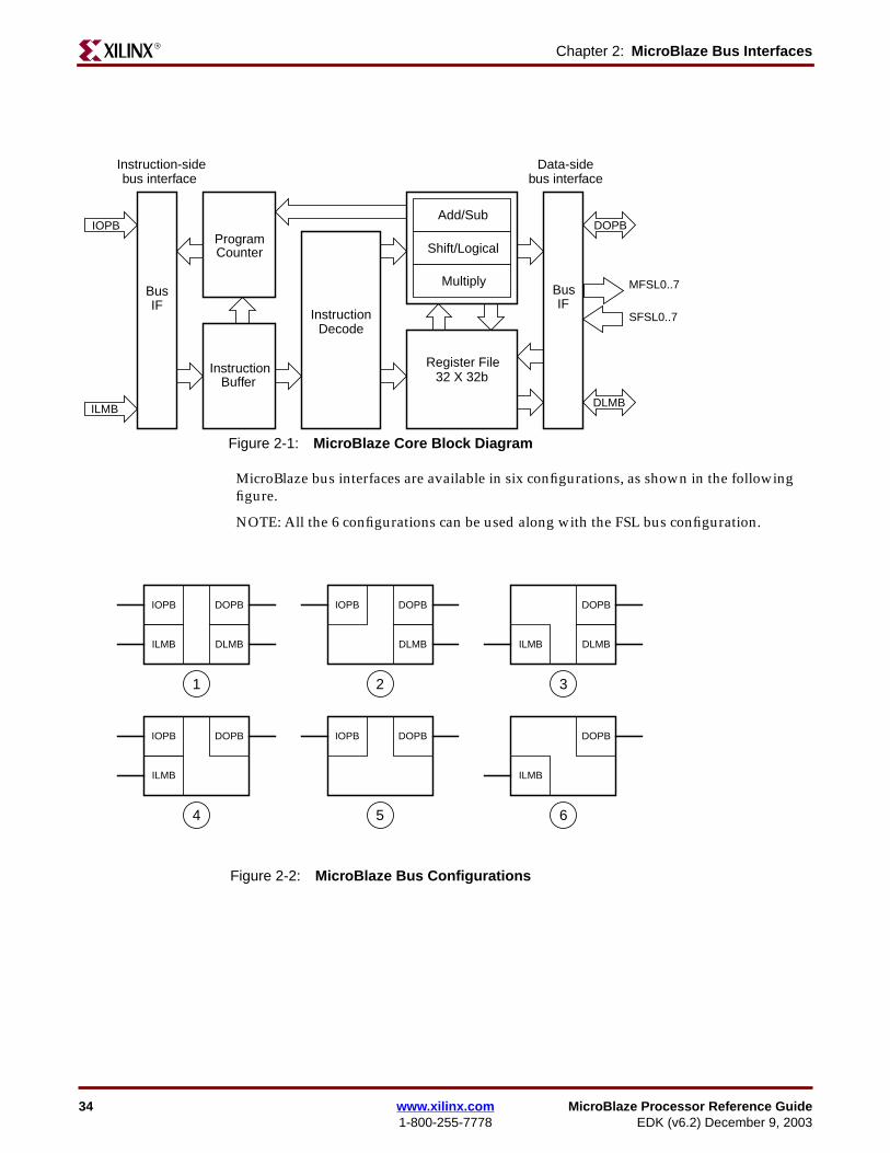
Bus ConfigurationsThe block diagram in Figure 2-1 depicts the MicroBlaze core with the bus interfacesdefined as follows:
DOPB: Data interface, On-chip Peripheral BusDLMB: Data interface, Local Memory Bus (BRAM only)IOPB: Instruction interface, On-chip Peripheral BusILMB: Instruction interface, Local Memory Bus (BRAM only)MFSL0..MFSL7: Master data interface, Fast Simplex LinkSFSL0..SFSL7: Slave data interface, Fast Simplex LinkCore: Miscellaneous signals (Clock, Reset, Interrupt)
34 www.xilinx.com MicroBlaze Processor Reference Guide1-800-255-7778 EDK (v6.2) December 9, 2003
Chapter 2: MicroBlaze Bus InterfacesR
MicroBlaze bus interfaces are available in six configurations, as shown in the followingfigure.
NOTE: All the 6 configurations can be used along with the FSL bus configuration.
Figure 2-1: MicroBlaze Core Block Diagram
Data-sideInstruction-side
DOPB
DLMB
IOPB
ILMB
bus interface bus interface
InstructionBuffer
ProgramCounter
Register File32 X 32b
Add/Sub
Shift/Logical
Multiply
InstructionDecode
BusIF
BusIF
MFSL0..7
SFSL0..7
Figure 2-2: MicroBlaze Bus Configurations
DOPB
DLMB
IOPB
ILMB
DOPB
DLMB
IOPB DOPB
DLMBILMB
DOPBIOPB
ILMB
DOPBIOPB DOPB
ILMB
1 2 3
4 5 6
MicroBlaze Processor Reference Guide www.xilinx.com 35EDK (v6.2) December 9, 2003 1-800-255-7778
Bus ConfigurationsR
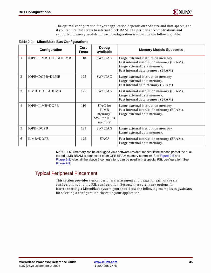
The optimal configuration for your application depends on code size and data spaces, andif you require fast access to internal block RAM. The performance implications andsupported memory models for each configuration is shown in the following table:
Note: ILMB memory can be debugged via a software resident monitor if the second port of the dual-ported ILMB BRAM is connected to an OPB BRAM memory controller. See Figure 2-6 andFigure 2-8. Also, all the above 6 confugrations can be used with a special FSL configuration. SeeFigure 2-9.
Typical Peripheral PlacementThis section provides typical peripheral placement and usage for each of the sixconfigurations and the FSL configuration. Because there are many options forinterconnecting a MicroBlaze system, you should use the following examples as guidelinesfor selecting a configuration closest to your application.
Table 2-1: MicroBlaze Bus Configurations
ConfigurationCoreFmax
Debugavailable
Memory Models Supported
1 IOPB+ILMB+DOPB+DLMB 110 SW/JTAG Large external instruction memory,Fast internal instruction memory (BRAM),Large external data memory,Fast internal data memory (BRAM)
2 IOPB+DOPB+DLMB 125 SW/JTAG Large external instruction memory,Large external data memory,Fast internal data memory (BRAM)
3 ILMB+DOPB+DLMB 125 SW/JTAG Fast internal instruction memory (BRAM),Large external data memory,Fast internal data memory (BRAM)
4 IOPB+ILMB+DOPB 110 JTAG forILMB
memory1
SW/for IOPBmemory
Large external instruction memory,Fast internal instruction memory (BRAM),Large external data memory,
5 IOPB+DOPB 125 SW/JTAG Large external instruction memory,Large external data memory,
6 ILMB+DOPB 125 JTAG1 Fast internal instruction memory (BRAM),Large external data memory,
36 www.xilinx.com MicroBlaze Processor Reference Guide1-800-255-7778 EDK (v6.2) December 9, 2003
Chapter 2: MicroBlaze Bus InterfacesR
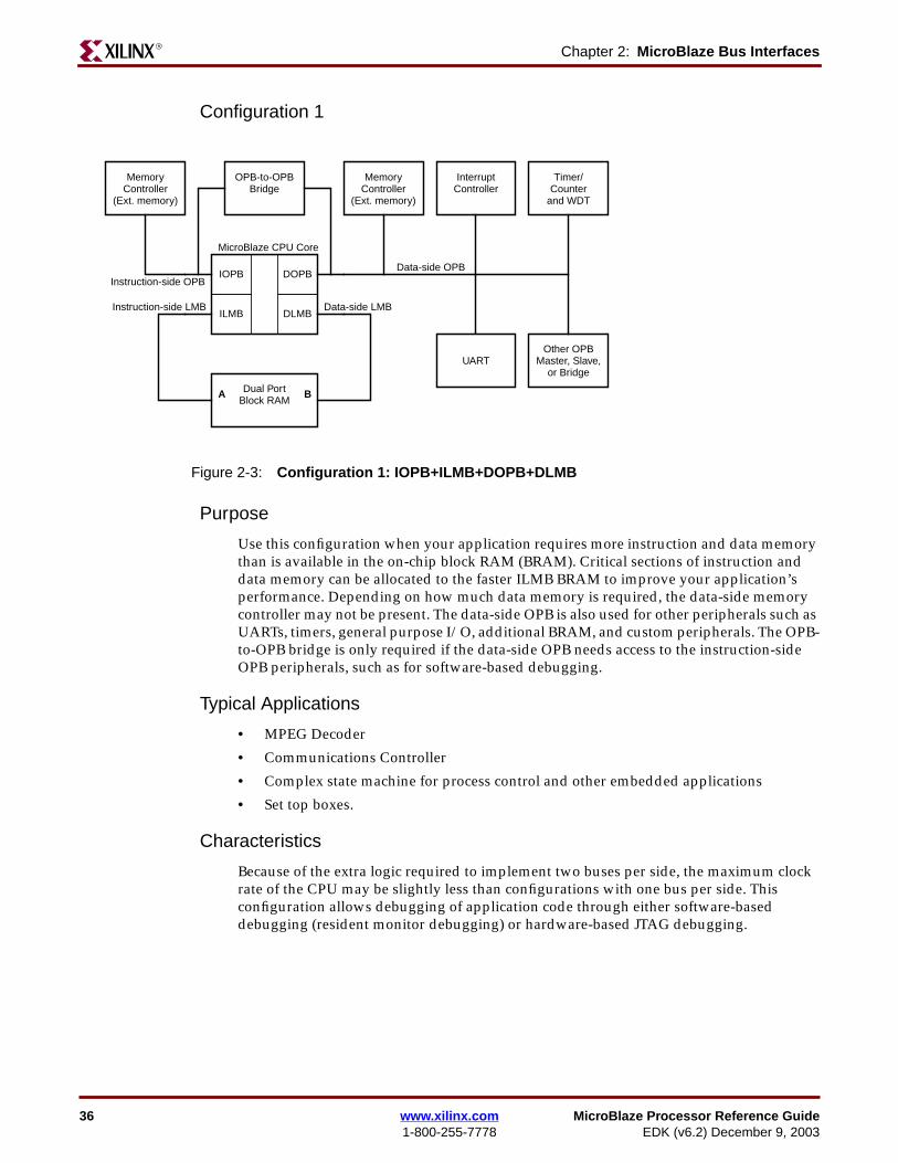
Configuration 1
Purpose
Use this configuration when your application requires more instruction and data memorythan is available in the on-chip block RAM (BRAM). Critical sections of instruction anddata memory can be allocated to the faster ILMB BRAM to improve your application’sperformance. Depending on how much data memory is required, the data-side memorycontroller may not be present. The data-side OPB is also used for other peripherals such asUARTs, timers, general purpose I/O, additional BRAM, and custom peripherals. The OPB-to-OPB bridge is only required if the data-side OPB needs access to the instruction-sideOPB peripherals, such as for software-based debugging.
Typical Applications
• MPEG Decoder
• Communications Controller
• Complex state machine for process control and other embedded applications
• Set top boxes.
Characteristics
Because of the extra logic required to implement two buses per side, the maximum clockrate of the CPU may be slightly less than configurations with one bus per side. Thisconfiguration allows debugging of application code through either software-baseddebugging (resident monitor debugging) or hardware-based JTAG debugging.
Figure 2-3: Configuration 1: IOPB+ILMB+DOPB+DLMB
DOPB
DLMB
IOPB
ILMB
Dual PortBlock RAM
A B
OPB-to-OPBBridge
MemoryController
(Ext. memory)
MemoryController
(Ext. memory)
InterruptController
Timer/Counter
and WDT
UARTOther OPB
Master, Slave,or Bridge
Data-side OPBInstruction-side OPB
Data-side LMBInstruction-side LMB
MicroBlaze CPU Core
MicroBlaze Processor Reference Guide www.xilinx.com 37EDK (v6.2) December 9, 2003 1-800-255-7778
Bus ConfigurationsR
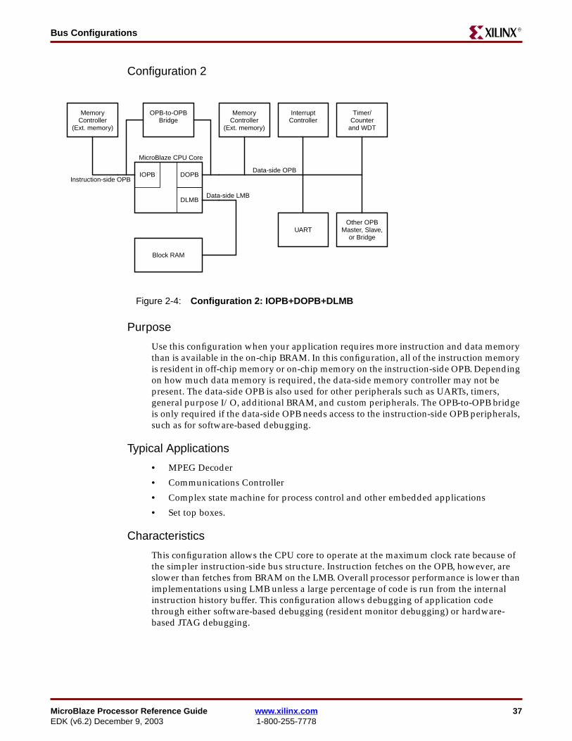
Configuration 2
Purpose
Use this configuration when your application requires more instruction and data memorythan is available in the on-chip BRAM. In this configuration, all of the instruction memoryis resident in off-chip memory or on-chip memory on the instruction-side OPB. Dependingon how much data memory is required, the data-side memory controller may not bepresent. The data-side OPB is also used for other peripherals such as UARTs, timers,general purpose I/O, additional BRAM, and custom peripherals. The OPB-to-OPB bridgeis only required if the data-side OPB needs access to the instruction-side OPB peripherals,such as for software-based debugging.
Typical Applications
• MPEG Decoder
• Communications Controller
• Complex state machine for process control and other embedded applications
• Set top boxes.
Characteristics
This configuration allows the CPU core to operate at the maximum clock rate because ofthe simpler instruction-side bus structure. Instruction fetches on the OPB, however, areslower than fetches from BRAM on the LMB. Overall processor performance is lower thanimplementations using LMB unless a large percentage of code is run from the internalinstruction history buffer. This configuration allows debugging of application codethrough either software-based debugging (resident monitor debugging) or hardware-based JTAG debugging.
Figure 2-4: Configuration 2: IOPB+DOPB+DLMB
DOPB
DLMB
IOPB
Block RAM
OPB-to-OPBBridge
MemoryController
(Ext. memory)
MemoryController
(Ext. memory)
InterruptController
Timer/Counter
and WDT
UARTOther OPB
Master, Slave,or Bridge
Data-side OPBInstruction-side OPB
Data-side LMB
MicroBlaze CPU Core
38 www.xilinx.com MicroBlaze Processor Reference Guide1-800-255-7778 EDK (v6.2) December 9, 2003
Chapter 2: MicroBlaze Bus InterfacesR
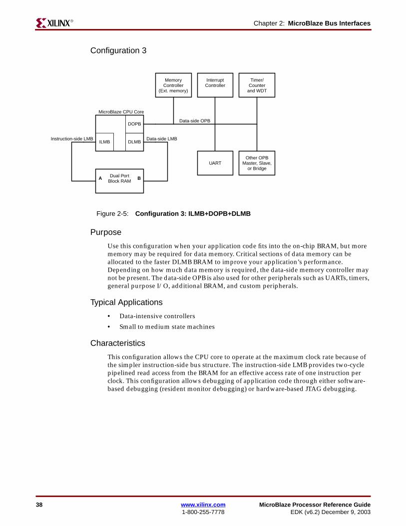
Configuration 3
Purpose
Use this configuration when your application code fits into the on-chip BRAM, but morememory may be required for data memory. Critical sections of data memory can beallocated to the faster DLMB BRAM to improve your application’s performance.Depending on how much data memory is required, the data-side memory controller maynot be present. The data-side OPB is also used for other peripherals such as UARTs, timers,general purpose I/O, additional BRAM, and custom peripherals.
Typical Applications
• Data-intensive controllers
• Small to medium state machines
Characteristics
This configuration allows the CPU core to operate at the maximum clock rate because ofthe simpler instruction-side bus structure. The instruction-side LMB provides two-cyclepipelined read access from the BRAM for an effective access rate of one instruction perclock. This configuration allows debugging of application code through either software-based debugging (resident monitor debugging) or hardware-based JTAG debugging.
Figure 2-5: Configuration 3: ILMB+DOPB+DLMB
DOPB
DLMBILMB
Dual PortBlock RAM
A B
MemoryController
(Ext. memory)
InterruptController
Timer/Counter
and WDT
UARTOther OPB
Master, Slave,or Bridge
Data-side OPB
Data-side LMBInstruction-side LMB
MicroBlaze CPU Core
MicroBlaze Processor Reference Guide www.xilinx.com 39EDK (v6.2) December 9, 2003 1-800-255-7778
Bus ConfigurationsR
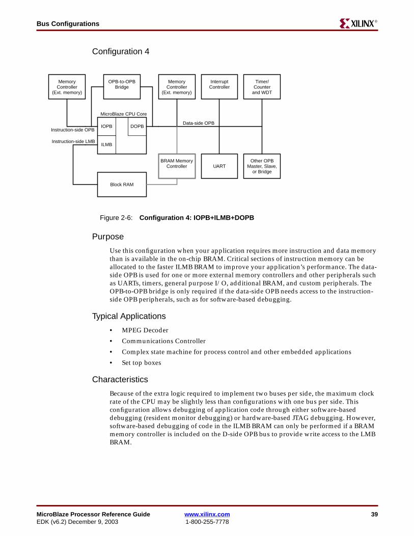
Configuration 4
Purpose
Use this configuration when your application requires more instruction and data memorythan is available in the on-chip BRAM. Critical sections of instruction memory can beallocated to the faster ILMB BRAM to improve your application’s performance. The data-side OPB is used for one or more external memory controllers and other peripherals suchas UARTs, timers, general purpose I/O, additional BRAM, and custom peripherals. TheOPB-to-OPB bridge is only required if the data-side OPB needs access to the instruction-side OPB peripherals, such as for software-based debugging.
Typical Applications
• MPEG Decoder
• Communications Controller
• Complex state machine for process control and other embedded applications
• Set top boxes
Characteristics
Because of the extra logic required to implement two buses per side, the maximum clockrate of the CPU may be slightly less than configurations with one bus per side. Thisconfiguration allows debugging of application code through either software-baseddebugging (resident monitor debugging) or hardware-based JTAG debugging. However,software-based debugging of code in the ILMB BRAM can only be performed if a BRAMmemory controller is included on the D-side OPB bus to provide write access to the LMBBRAM.
Figure 2-6: Configuration 4: IOPB+ILMB+DOPB
DOPBIOPB
ILMB
Block RAM
OPB-to-OPBBridge
MemoryController
(Ext. memory)
MemoryController
(Ext. memory)
InterruptController
Timer/Counter
and WDT
UARTOther OPB
Master, Slave,or Bridge
Data-side OPBInstruction-side OPB
Instruction-side LMB
MicroBlaze CPU Core
BRAM MemoryController
40 www.xilinx.com MicroBlaze Processor Reference Guide1-800-255-7778 EDK (v6.2) December 9, 2003
Chapter 2: MicroBlaze Bus InterfacesR
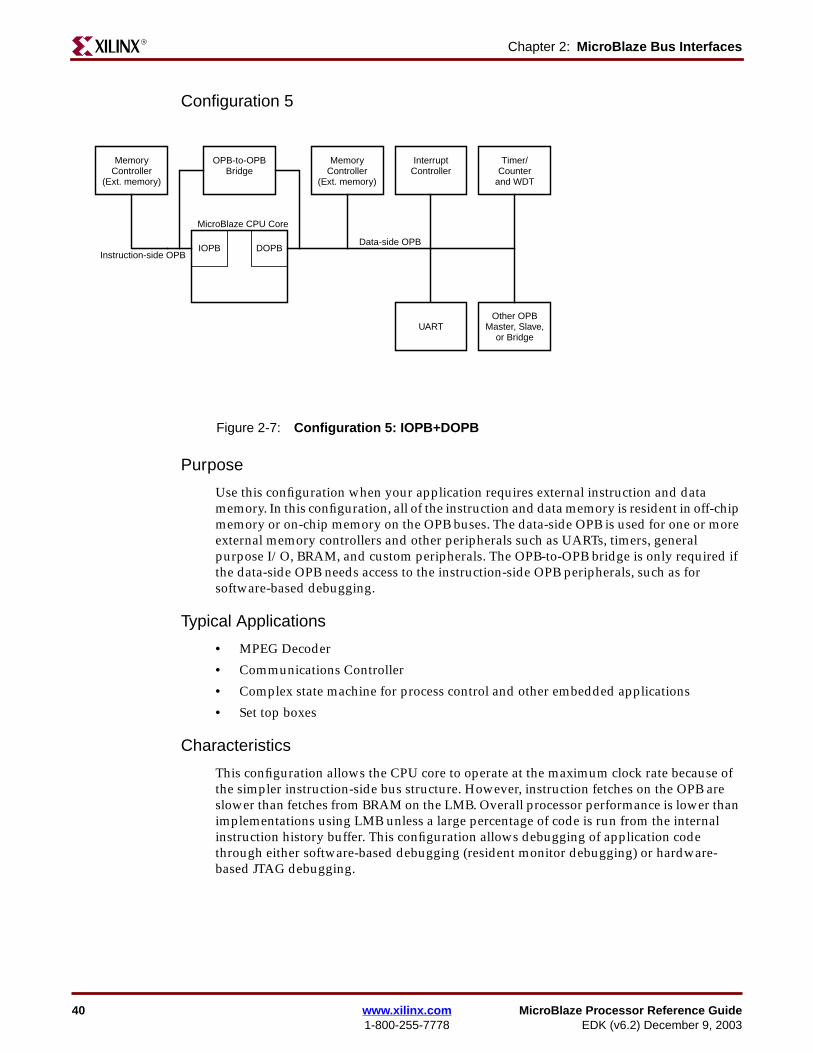
Configuration 5
Purpose
Use this configuration when your application requires external instruction and datamemory. In this configuration, all of the instruction and data memory is resident in off-chipmemory or on-chip memory on the OPB buses. The data-side OPB is used for one or moreexternal memory controllers and other peripherals such as UARTs, timers, generalpurpose I/O, BRAM, and custom peripherals. The OPB-to-OPB bridge is only required ifthe data-side OPB needs access to the instruction-side OPB peripherals, such as forsoftware-based debugging.
Typical Applications
• MPEG Decoder
• Communications Controller
• Complex state machine for process control and other embedded applications
• Set top boxes
Characteristics
This configuration allows the CPU core to operate at the maximum clock rate because ofthe simpler instruction-side bus structure. However, instruction fetches on the OPB areslower than fetches from BRAM on the LMB. Overall processor performance is lower thanimplementations using LMB unless a large percentage of code is run from the internalinstruction history buffer. This configuration allows debugging of application codethrough either software-based debugging (resident monitor debugging) or hardware-based JTAG debugging.
Figure 2-7: Configuration 5: IOPB+DOPB
DOPBIOPB
OPB-to-OPBBridge
MemoryController
(Ext. memory)
MemoryController
(Ext. memory)
InterruptController
Timer/Counter
and WDT
UARTOther OPB
Master, Slave,or Bridge
Data-side OPBInstruction-side OPB
MicroBlaze CPU Core
MicroBlaze Processor Reference Guide www.xilinx.com 41EDK (v6.2) December 9, 2003 1-800-255-7778
Bus ConfigurationsR
Configuration 6
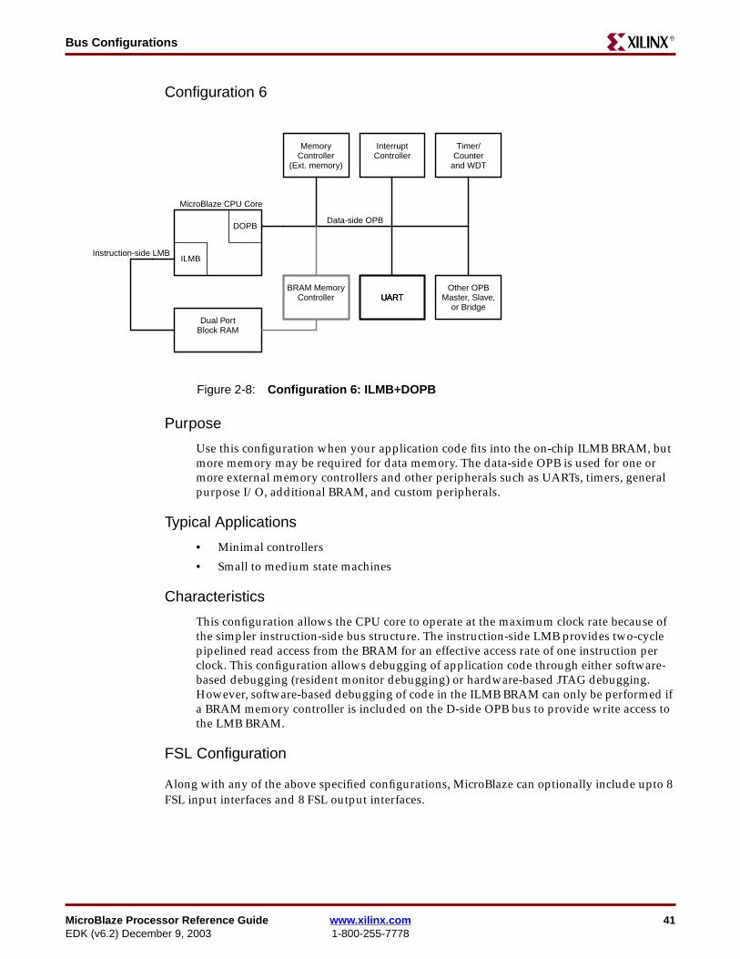
Purpose
Use this configuration when your application code fits into the on-chip ILMB BRAM, butmore memory may be required for data memory. The data-side OPB is used for one ormore external memory controllers and other peripherals such as UARTs, timers, generalpurpose I/O, additional BRAM, and custom peripherals.
Typical Applications
• Minimal controllers
• Small to medium state machines
Characteristics
This configuration allows the CPU core to operate at the maximum clock rate because ofthe simpler instruction-side bus structure. The instruction-side LMB provides two-cyclepipelined read access from the BRAM for an effective access rate of one instruction perclock. This configuration allows debugging of application code through either software-based debugging (resident monitor debugging) or hardware-based JTAG debugging.However, software-based debugging of code in the ILMB BRAM can only be performed ifa BRAM memory controller is included on the D-side OPB bus to provide write access tothe LMB BRAM.
FSL Configuration
Along with any of the above specified configurations, MicroBlaze can optionally include upto 8FSL input interfaces and 8 FSL output interfaces.
Figure 2-8: Configuration 6: ILMB+DOPB
DOPB
ILMB
Dual PortBlock RAM
MemoryController
(Ext. memory)
InterruptController
Timer/Counter
and WDT
UARTOther OPB
Master, Slave,or Bridge
Data-side OPB
Instruction-side LMB
MicroBlaze CPU Core
UARTUARTBRAM Memory
Controller
42 www.xilinx.com MicroBlaze Processor Reference Guide1-800-255-7778 EDK (v6.2) December 9, 2003
Chapter 2: MicroBlaze Bus InterfacesR
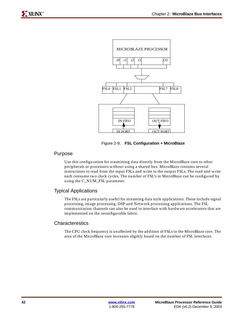
Purpose
Use this configuration for trasmitting data directly from the MicroBlaze core to otherperipherals or processors without using a shared bus. MicroBlaze contains severalinstructions to read from the input FSLs and write to the output FSLs. The read and writeeach consume two clock cycles. The number of FSL’s in MicroBlaze can be configured byusing the C_NUM_FSL parameter.
Typical Applications
The FSLs are particularly useful for streaming data style applications. These include signalprocessing, image processing, DSP and Network processing applications. The FSLcommunication channels can also be used to interface with hardware accelerators that areimplemented on the reconfigurable fabric.
Characterestics
The CPU clock frequency is unaffected by the addition of FSLs to the MicroBlaze core. Thearea of the MicroBlaze core increases sligthly based on the number of FSL interfaces.
Figure 2-9: FSL Configuration + MicroBlaze
IN FIFO OUT FIFO
IN PORT OUT PORT
FSL0 FSL1 FSL2 FSL7 FSL8
r0 r1 r2 r3 r32
MICROBLAZE PROCESSOR
MicroBlaze Processor Reference Guide www.xilinx.com 43EDK (v6.2) December 9, 2003 1-800-255-7778
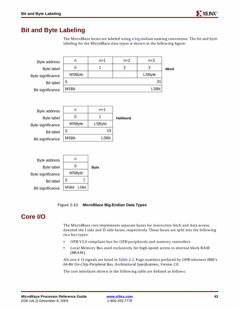
Bit and Byte LabelingR
Bit and Byte LabelingThe MicroBlaze buses are labeled using a big-endian naming convention. The bit and bytelabeling for the MicroBlaze data types is shown in the following figure:
Core I/OThe MicroBlaze core implements separate buses for instruction fetch and data access,denoted the I side and D side buses, respectively. These buses are split into the followingtwo bus types:
• OPB V2.0 compliant bus for OPB peripherals and memory controllers
• Local Memory Bus used exclusively for high-speed access to internal block RAM(BRAM).
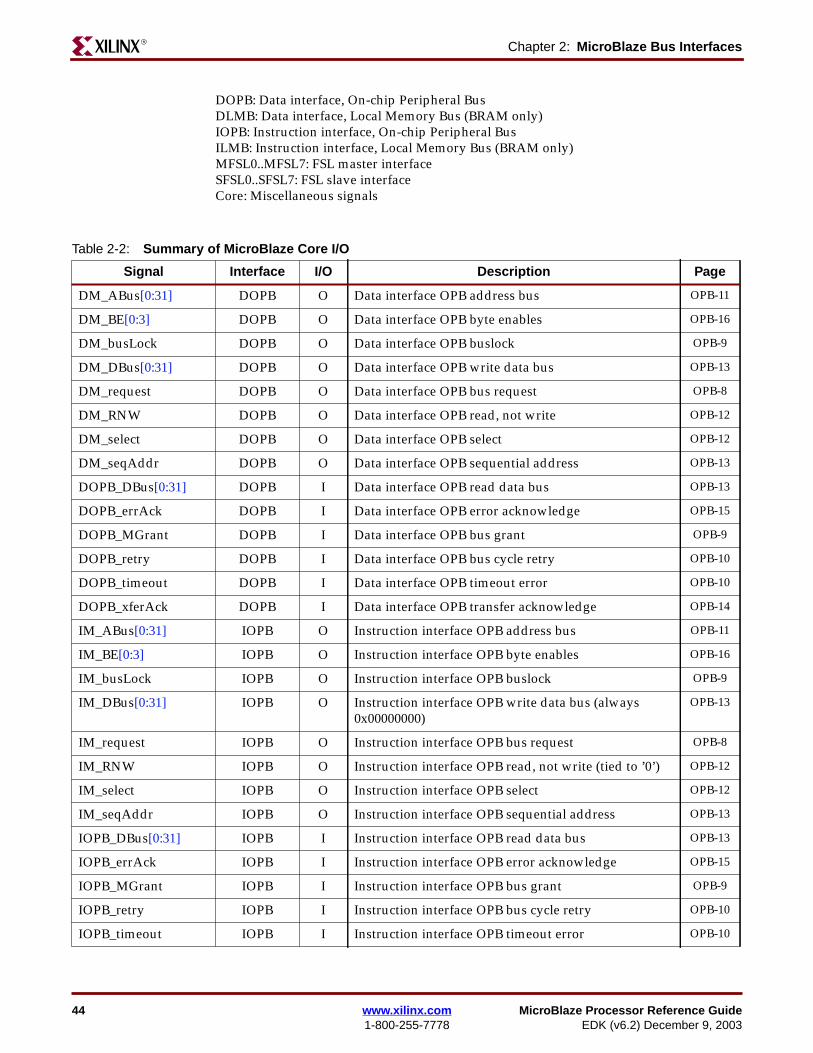
All core I/O signals are listed in Table 2-2. Page numbers prefaced by OPB reference IBM’s64-Bit On-Chip Peripheral Bus, Architectural Specifications, Version 2.0.
The core interfaces shown in the following table are defined as follows:
Figure 2-10: MicroBlaze Big-Endian Data Types
n n+1 n+2 n+3
0 1 2 3
MSByte LSByte
0 31
MSBit LSBit
Byte address
Byte label
Byte significance
Bit label
Bit significance
n n+1
0 1
MSByte LSByte
0 15
MSBit LSBit
Byte address
Byte label
Byte significance
Bit label
Bit significance
n
0
MSByte
0 7
MSBit LSBit
Byte address
Byte label
Byte significance
Bit label
Bit significance
Byte
Halfword
Word
44 www.xilinx.com MicroBlaze Processor Reference Guide1-800-255-7778 EDK (v6.2) December 9, 2003
Chapter 2: MicroBlaze Bus InterfacesR
DOPB: Data interface, On-chip Peripheral BusDLMB: Data interface, Local Memory Bus (BRAM only)IOPB: Instruction interface, On-chip Peripheral BusILMB: Instruction interface, Local Memory Bus (BRAM only)MFSL0..MFSL7: FSL master interfaceSFSL0..SFSL7: FSL slave interfaceCore: Miscellaneous signals
Table 2-2: Summary of MicroBlaze Core I/O
Signal Interface I/O Description Page
DM_ABus[0:31] DOPB O Data interface OPB address bus OPB-11
DM_BE[0:3] DOPB O Data interface OPB byte enables OPB-16
DM_busLock DOPB O Data interface OPB buslock OPB-9
DM_DBus[0:31] DOPB O Data interface OPB write data bus OPB-13
DM_request DOPB O Data interface OPB bus request OPB-8
DM_RNW DOPB O Data interface OPB read, not write OPB-12
DM_select DOPB O Data interface OPB select OPB-12
DM_seqAddr DOPB O Data interface OPB sequential address OPB-13
DOPB_DBus[0:31] DOPB I Data interface OPB read data bus OPB-13
DOPB_errAck DOPB I Data interface OPB error acknowledge OPB-15
DOPB_MGrant DOPB I Data interface OPB bus grant OPB-9
DOPB_retry DOPB I Data interface OPB bus cycle retry OPB-10
DOPB_timeout DOPB I Data interface OPB timeout error OPB-10
DOPB_xferAck DOPB I Data interface OPB transfer acknowledge OPB-14
IM_ABus[0:31] IOPB O Instruction interface OPB address bus OPB-11
IM_BE[0:3] IOPB O Instruction interface OPB byte enables OPB-16
IM_busLock IOPB O Instruction interface OPB buslock OPB-9
IM_DBus[0:31] IOPB O Instruction interface OPB write data bus (always0x00000000)
OPB-13
IM_request IOPB O Instruction interface OPB bus request OPB-8
IM_RNW IOPB O Instruction interface OPB read, not write (tied to ’0’) OPB-12
IM_select IOPB O Instruction interface OPB select OPB-12
IM_seqAddr IOPB O Instruction interface OPB sequential address OPB-13
IOPB_DBus[0:31] IOPB I Instruction interface OPB read data bus OPB-13
IOPB_errAck IOPB I Instruction interface OPB error acknowledge OPB-15
IOPB_MGrant IOPB I Instruction interface OPB bus grant OPB-9
IOPB_retry IOPB I Instruction interface OPB bus cycle retry OPB-10
IOPB_timeout IOPB I Instruction interface OPB timeout error OPB-10
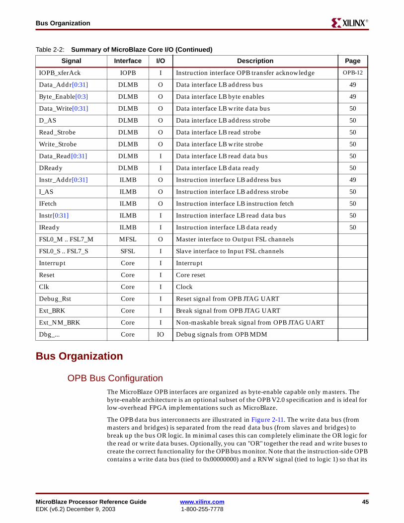
MicroBlaze Processor Reference Guide www.xilinx.com 45EDK (v6.2) December 9, 2003 1-800-255-7778
Bus OrganizationR
Bus Organization
OPB Bus ConfigurationThe MicroBlaze OPB interfaces are organized as byte-enable capable only masters. Thebyte-enable architecture is an optional subset of the OPB V2.0 specification and is ideal forlow-overhead FPGA implementations such as MicroBlaze.
The OPB data bus interconnects are illustrated in Figure 2-11. The write data bus (frommasters and bridges) is separated from the read data bus (from slaves and bridges) tobreak up the bus OR logic. In minimal cases this can completely eliminate the OR logic forthe read or write data buses. Optionally, you can "OR" together the read and write buses tocreate the correct functionality for the OPB bus monitor. Note that the instruction-side OPBcontains a write data bus (tied to 0x00000000) and a RNW signal (tied to logic 1) so that its
IOPB_xferAck IOPB I Instruction interface OPB transfer acknowledge OPB-12
Data_Addr[0:31] DLMB O Data interface LB address bus 49
Byte_Enable[0:3] DLMB O Data interface LB byte enables 49
Data_Write[0:31] DLMB O Data interface LB write data bus 50
D_AS DLMB O Data interface LB address strobe 50
Read_Strobe DLMB O Data interface LB read strobe 50
Write_Strobe DLMB O Data interface LB write strobe 50
Data_Read[0:31] DLMB I Data interface LB read data bus 50
DReady DLMB I Data interface LB data ready 50
Instr_Addr[0:31] ILMB O Instruction interface LB address bus 49
I_AS ILMB O Instruction interface LB address strobe 50
IFetch ILMB O Instruction interface LB instruction fetch 50
Instr[0:31] ILMB I Instruction interface LB read data bus 50
IReady ILMB I Instruction interface LB data ready 50
FSL0_M .. FSL7_M MFSL O Master interface to Output FSL channels
FSL0_S .. FSL7_S SFSL I Slave interface to Input FSL channels
Interrupt Core I Interrupt
Reset Core I Core reset
Clk Core I Clock
Debug_Rst Core I Reset signal from OPB JTAG UART
Ext_BRK Core I Break signal from OPB JTAG UART
Ext_NM_BRK Core I Non-maskable break signal from OPB JTAG UART
Dbg_... Core IO Debug signals from OPB MDM
Table 2-2: Summary of MicroBlaze Core I/O (Continued)
Signal Interface I/O Description Page
46 www.xilinx.com MicroBlaze Processor Reference Guide1-800-255-7778 EDK (v6.2) December 9, 2003
Chapter 2: MicroBlaze Bus InterfacesR
interface remains consistent with the data-side OPB. These signals are constant andgenerally are minimized in implementation.
A multi-ported slave is used instead of a bridge in the example shown in Figure 2-12. Thiscould represent a memory controller with a connection to both the IOPB and the DOPB. Inthis case, the bus multiplexing and prioritization must be done in the slave. The advantageof this approach is that a separate I-to-D bridge and an OPB arbiter on the instruction sideare not required. The arbiter function must still exist in the slave device.

MicroBlaze Processor Reference Guide www.xilinx.com 47EDK (v6.2) December 9, 2003 1-800-255-7778
Bus OrganizationR
Figure 2-11: OPB Interconnection (breaking up read and write buses)
DM_ABus[0:31]DM_BE[0:3]DM_busLockDM_wrDBus[0:31]DM_RNWDM_selectDM_seqAddr
DOPB_ABus[0:31]DOPB_BE[0:3]DOPB_busLockDOPB_wrDBus[0:31]
DOPB_RNWDOPB_selectDOPB_seqAddrDOPB_errAckDOPB_retryDOPB_timeoutDOPB_toutSupDOPB_xferAck
DOPB_ABus[0:31]DOPB_BE[0:3]DOPB_busLock
DOPB_rdDBus[0:31]
DOPB_RNWDOPB_selectDOPB_seqAddr
DOPB_errAckDOPB_retryDOPB_timeoutDOPB_xferAck
DOPB_wrDBus[0:31]
Sl1_rdDBus[0:31]Sl1_errAckSl1_retrySl1_timeoutSl1_toutSupSl1_xferAck
DOPB_ABus[0:31]DOPB_BE[0:3]DOPB_busLock
DOPB_RNWDOPB_selectDOPB_seqAddr
DOPB_wrDBus[0:31]
Br1I_rdDBus[0:31]Br1_errAckBr1_retryBr1_timeout
Br1_ABus[0:31]Br1_BE[0:3]Br1_busLockBr1D_wrDBus[0:31]Br1_RNWBr1_selectBr1_seqAddr
IOPB_rdDBus[0:31]IOPB_errAckIOPB_retryIOPB_timeoutIOPB_toutSup
IM_ABus[0:31]IM_BE[0:3]IM_busLock
IM_RNWIM_selectIM_seqAddr
IOPB_rdDBus[0:31]IOPB_errAckIOPB_retryIOPB_timeoutIOPB_xferAck
IOPB_ABus[0:31]IOPB_BE[0:3]IOPB_busLock
IOPB_RNWIOPB_selectIOPB_seqAddr
IOPB_wrDBus[0:31]
Sl2_rdDBus[0:31]Sl2_errAckSl2_retrySl2_timeoutSl2_toutSupSl2_xferAck
IOPB_ABus[0:31]IOPB_BE[0:3]IOPB_busLockIOPB_wrDBus[0:31]
IOPB_RNWIOPB_selectIOPB_seqAddrIOPB_errAckIOPB_retryIOPB_timeoutIOPB_toutSupIOPB_xferAck
Br1_toutSup
MicroBlazeData OPBInterface
OPBSlave1
MicroBlazeInstr OPBInterface
(IOPB)
OPBSlave2
DOPBto
IOPB
OR
like
suffixes
OR
like
suffixes
DOPB_rdDBus[0:31]
IOPB_rdDBus[0:31]
ORIOPB_wrDBus[0:31]IOPB_rdDBus[0:31]
IOPB_DBus[0:31]
ORDOPB_wrDBus[0:31]DOPB_rdDBus[0:31]
DOPB_DBus[0:31]
Present for Bus Monitor functions:
Present for Bus Monitor functions:
Data-side OPB
Instruction-side OPB
I-sideOPB
arbiter
D-sideOPB
arbiter
Required if more thanone master present
Required
Br1_xferAckIOPB_xferAck
IM_wrDBus[0:31]
DM_requestDOPB_MGrant
IM_requestIOPB_MGrant
Br1_requestBr1_MGrant
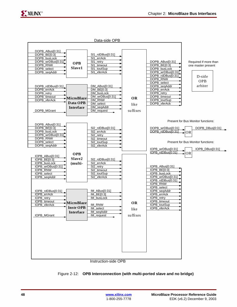
48 www.xilinx.com MicroBlaze Processor Reference Guide1-800-255-7778 EDK (v6.2) December 9, 2003
Chapter 2: MicroBlaze Bus InterfacesR
Figure 2-12: OPB Interconnection (with multi-ported slave and no bridge)
DM_ABus[0:31]DM_BE[0:3]DM_busLockDM_wrDBus[0:31]DM_RNWDM_selectDM_seqAddr
DOPB_ABus[0:31]DOPB_BE[0:3]DOPB_busLockDOPB_wrDBus[0:31]
DOPB_RNWDOPB_selectDOPB_seqAddrDOPB_errAckDOPB_retryDOPB_timeoutDOPB_toutSupDOPB_xferAck
DOPB_ABus[0:31]DOPB_BE[0:3]DOPB_busLock
DOPB_rdDBus[0:31]
DOPB_RNWDOPB_selectDOPB_seqAddr
DOPB_errAckDOPB_retryDOPB_timeoutDOPB_xferAck
DOPB_wrDBus[0:31]
Sl1_rdDBus[0:31]Sl1_errAckSl1_retrySl1_timeoutSl1_toutSupSl1_xferAck
DOPB_ABus[0:31]DOPB_BE[0:3]DOPB_busLock
DOPB_RNWDOPB_selectDOPB_seqAddr
DOPB_wrDBus[0:31]
IM_ABus[0:31]IM_BE[0:3]IM_busLock
IM_RNWIM_selectIM_seqAddr
IOPB_rdDBus[0:31]IOPB_errAckIOPB_retryIOPB_timeoutIOPB_xferAck
IOPB_ABus[0:31]IOPB_BE[0:3]IOPB_busLock
IOPB_RNWIOPB_selectIOPB_seqAddr
IOPB_wrDBus[0:31]
Sl2_rdDBus[0:31]Sl2_errAckSl2_retrySl2_timeoutSl2_toutSupSl2_xferAck
IOPB_ABus[0:31]IOPB_BE[0:3]IOPB_busLockIOPB_wrDBus[0:31]
IOPB_RNWIOPB_selectIOPB_seqAddrIOPB_errAckIOPB_retryIOPB_timeoutIOPB_toutSupIOPB_xferAck
MicroBlazeData OPBInterface
OPBSlave1
MicroBlazeInstr OPBInterface
OR
like
suffixes
OR
like
suffixes
DOPB_rdDBus[0:31]
IOPB_rdDBus[0:31]
ORIOPB_wrDBus[0:31]IOPB_rdDBus[0:31]
IOPB_DBus[0:31]
ORDOPB_wrDBus[0:31]DOPB_rdDBus[0:31]
DOPB_DBus[0:31]
Present for Bus Monitor functions:
Present for Bus Monitor functions:
Data-side OPB
Instruction-side OPB
Sl2_rdDBus[0:31]Sl2_errAckSl2_retrySl2_timeoutSl2_toutSupSl2_xferAck
OPBSlave2(multi-
D-sideOPB
arbiter
Required if more thanone master present
DM_requestDOPB_MGrant
IM_requestIOPB_MGrant
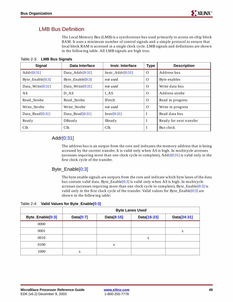
MicroBlaze Processor Reference Guide www.xilinx.com 49EDK (v6.2) December 9, 2003 1-800-255-7778
Bus OrganizationR
LMB Bus DefinitionThe Local Memory Bus (LMB) is a synchronous bus used primarily to access on-chip blockRAM. It uses a minimum number of control signals and a simple protocol to ensure thatlocal block RAM is accessed in a single clock cycle. LMB signals and definitions are shownin the following table. All LMB signals are high true.
Addr[0:31]
The address bus is an output from the core and indicates the memory address that is beingaccessed by the current transfer. It is valid only when AS is high. In multicycle accesses(accesses requiring more than one clock cycle to complete), Addr[0:31] is valid only in thefirst clock cycle of the transfer.
Byte_Enable[0:3]
The byte enable signals are outputs from the core and indicate which byte lanes of the databus contain valid data. Byte_Enable[0:3] is valid only when AS is high. In multicycleaccesses (accesses requiring more than one clock cycle to complete), Byte_Enable[0:3] isvalid only in the first clock cycle of the transfer. Valid values for Byte_Enable[0:3] areshown in the following table:
Table 2-3: LMB Bus Signals
Signal Data Interface Instr. Interface Type Description
Addr[0:31] Data_Addr[0:31] Instr_Addr[0:31] O Address bus
Byte_Enable[0:3] Byte_Enable[0:3] not used O Byte enables
Data_Write[0:31] Data_Write[0:31] not used O Write data bus
AS D_AS I_AS O Address strobe
Read_Strobe Read_Strobe IFetch O Read in progress
Write_Strobe Write_Strobe not used O Write in progress
Data_Read[0:31] Data_Read[0:31] Instr[0:31] I Read data bus
Ready DReady IReady I Ready for next transfer
Clk Clk Clk I Bus clock
Table 2-4: Valid Values for Byte_Enable[0:3]
Byte Lanes Used
Byte_Enable[0:3] Data[0:7] Data[8:15] Data[16:23] Data[24:31]
0000
0001 x
0010 x
0100 x
1000 x
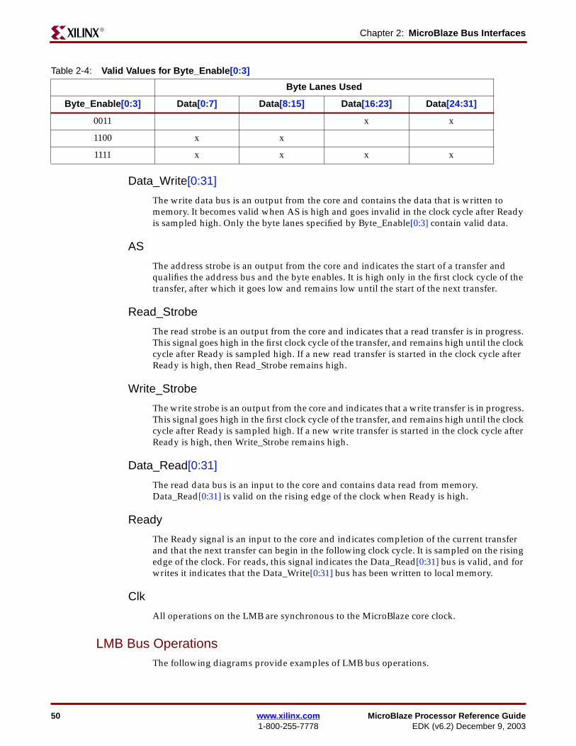
50 www.xilinx.com MicroBlaze Processor Reference Guide1-800-255-7778 EDK (v6.2) December 9, 2003
Chapter 2: MicroBlaze Bus InterfacesR
Data_Write[0:31]
The write data bus is an output from the core and contains the data that is written tomemory. It becomes valid when AS is high and goes invalid in the clock cycle after Readyis sampled high. Only the byte lanes specified by Byte_Enable[0:3] contain valid data.
AS
The address strobe is an output from the core and indicates the start of a transfer andqualifies the address bus and the byte enables. It is high only in the first clock cycle of thetransfer, after which it goes low and remains low until the start of the next transfer.
Read_Strobe
The read strobe is an output from the core and indicates that a read transfer is in progress.This signal goes high in the first clock cycle of the transfer, and remains high until the clockcycle after Ready is sampled high. If a new read transfer is started in the clock cycle afterReady is high, then Read_Strobe remains high.
Write_Strobe
The write strobe is an output from the core and indicates that a write transfer is in progress.This signal goes high in the first clock cycle of the transfer, and remains high until the clockcycle after Ready is sampled high. If a new write transfer is started in the clock cycle afterReady is high, then Write_Strobe remains high.
Data_Read[0:31]
The read data bus is an input to the core and contains data read from memory.Data_Read[0:31] is valid on the rising edge of the clock when Ready is high.
Ready
The Ready signal is an input to the core and indicates completion of the current transferand that the next transfer can begin in the following clock cycle. It is sampled on the risingedge of the clock. For reads, this signal indicates the Data_Read[0:31] bus is valid, and forwrites it indicates that the Data_Write[0:31] bus has been written to local memory.
Clk
All operations on the LMB are synchronous to the MicroBlaze core clock.
LMB Bus OperationsThe following diagrams provide examples of LMB bus operations.
0011 x x
1100 x x
1111 x x x x
Table 2-4: Valid Values for Byte_Enable[0:3]
Byte Lanes Used
Byte_Enable[0:3] Data[0:7] Data[8:15] Data[16:23] Data[24:31]
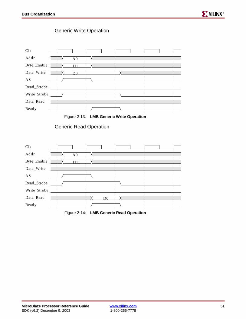
MicroBlaze Processor Reference Guide www.xilinx.com 51EDK (v6.2) December 9, 2003 1-800-255-7778
Bus OrganizationR
Generic Write Operation
Generic Read Operation
Figure 2-13: LMB Generic Write Operation
Clk
Addr
Byte_Enable
Data_Write
AS
Read_Strobe
Write_Strobe
Data_Read
Ready
A0
1111
D0
Figure 2-14: LMB Generic Read Operation
Clk
Addr
Byte_Enable
Data_Write
AS
Read_Strobe
Write_Strobe
Data_Read
Ready
A0
1111
D0
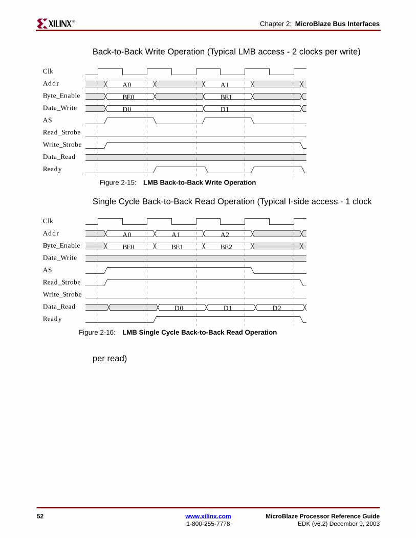
52 www.xilinx.com MicroBlaze Processor Reference Guide1-800-255-7778 EDK (v6.2) December 9, 2003
Chapter 2: MicroBlaze Bus InterfacesR
Back-to-Back Write Operation (Typical LMB access - 2 clocks per write)
Single Cycle Back-to-Back Read Operation (Typical I-side access - 1 clock
per read)
Figure 2-15: LMB Back-to-Back Write Operation
Figure 2-16: LMB Single Cycle Back-to-Back Read Operation
Clk
Addr
Byte_Enable
Data_Write
AS
Read_Strobe
Write_Strobe
Data_Read
Ready
A0 A1
BE0 BE1
D0 D1
Clk
Addr
Byte_Enable
Data_Write
AS
Read_Strobe
Write_Strobe
Data_Read
Ready
A0 A1 A2
BE0 BE1 BE2
D0 D1 D2
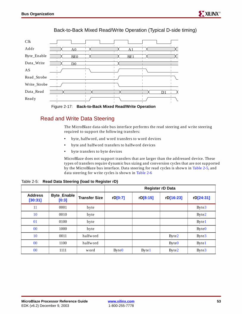
MicroBlaze Processor Reference Guide www.xilinx.com 53EDK (v6.2) December 9, 2003 1-800-255-7778
Bus OrganizationR
Back-to-Back Mixed Read/Write Operation (Typical D-side timing)
Read and Write Data SteeringThe MicroBlaze data-side bus interface performs the read steering and write steeringrequired to support the following transfers:
• byte, halfword, and word transfers to word devices
• byte and halfword transfers to halfword devices
• byte transfers to byte devices
MicroBlaze does not support transfers that are larger than the addressed device. Thesetypes of transfers require dynamic bus sizing and conversion cycles that are not supportedby the MicroBlaze bus interface. Data steering for read cycles is shown in Table 2-5, anddata steering for write cycles is shown in Table 2-6
Figure 2-17: Back-to-Back Mixed Read/Write Operation
Clk
Addr
Byte_Enable
Data_Write
AS
Read_Strobe
Write_Strobe
Data_Read
Ready
A0 A1
BE0 BE1
D1
D0
Table 2-5: Read Data Steering (load to Register rD)
Register rD Data
Address[30:31]
Byte_Enable[0:3]
Transfer Size rD[0:7] rD[8:15] rD[16:23] rD[24:31]
11 0001 byte Byte3
10 0010 byte Byte2
01 0100 byte Byte1
00 1000 byte Byte0
10 0011 halfword Byte2 Byte3
00 1100 halfword Byte0 Byte1
00 1111 word Byte0 Byte1 Byte2 Byte3
54 www.xilinx.com MicroBlaze Processor Reference Guide1-800-255-7778 EDK (v6.2) December 9, 2003
Chapter 2: MicroBlaze Bus InterfacesR
Note that other OPB masters may have more restrictive requirements for byte laneplacement than those allowed by MicroBlaze. OPB slave devices are typically attached"left-justified" with byte devices attached to the most-significant byte lane, and halfworddevices attached to the most significant halfword lane. The MicroBlaze steering logic fullysupports this attachment method.
FSL Bus OperationThe Fast Simplex Link bus provides a point-to-point communication channel between anoutput FIFO and an input FIFO. For more information on the FSL bus, please refer to theFSL bus documentation available in the Processor IP reference guide.
Master FSL signals on MicroBlaze
MicroBlaze may contain upto 8 master FSL interfaces. The master signals are depicted inTable 2-7.
Table 2-6: Write Data Steering (store from Register rD)
Write Data Bus Bytes
Address[30:31]
Byte_Enable[0:3]
Transfer Size Byte0 Byte1 Byte2 Byte3
11 0001 byte rD[24:31]
10 0010 byte rD[24:31]
01 0100 byte rD[24:31]
00 1000 byte rD[24:31]
10 0011 halfword rD[16:23] rD[24:31]
00 1100 halfword rD[16:23] rD[24:31]
00 1111 word rD[0:7] rD[8:15] rD[16:23] rD[24:31]
Table 2-7: Master FSL signals
Signal Name Description VHDL Type Direction
FSLn_M_Clk Clock std_logic input
FSLn_M_Write Write enable signal thatindicating data is ready to bewritten to the output FSLwhen set
std_logic output
FSLn_M_Data Data value written to theoutput FSL
std_logic_vector output
FSLn_M_CONTROL Control bit value written tothe output FSL
std_logic output
FSLn_M_FULL Full Bit indicating outputFSL FIFO is full when set
std_logic input
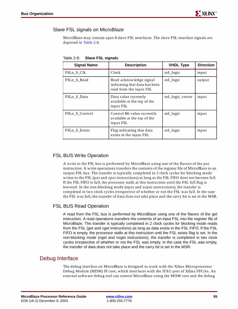
MicroBlaze Processor Reference Guide www.xilinx.com 55EDK (v6.2) December 9, 2003 1-800-255-7778
Bus OrganizationR
Slave FSL signals on MicroBlaze
MicroBlaze may contain upto 8 slave FSL interfaces. The slave FSL interface signals aredepicted in Table 2-8.
FSL BUS Write Operation
A write to the FSL bus is performed by MicroBlaze using one of the flavors of the putinstruction. A write operations transfers the contents of the register file of MicroBlaze to anoutput FSL bus. The transfer is typically completed in 2 clock cycles for blocking modewrites to the FSL (put and cput instructions) as long as the FSL FIFO does not become full.If the FSL FIFO is full, the processor stalls at this instruction until the FSL full flag islowered. In the non-blocking mode (nput and ncput instructions), the transfer iscompleted in two clock cycles irrespective of whether or not the FSL was full. In the casethe FSL was full, the transfer of data does not take place and the carry bit is set in the MSR.
FSL BUS Read Operation
A read from the FSL bus is performed by MicroBlaze using one of the flavors of the getinstruction. A read operations transfers the contents of an input FSL into the register file ofMicroBlaze. The transfer is typically completed in 2 clock cycles for blocking mode readsfrom the FSL (get and cget instructions) as long as data exists in the FSL FIFO. If the FSLFIFO is empty, the processor stalls at this instruction until the FSL exists flag is set. In thenon-blocking mode (nget and ncget instructions), the transfer is completed in two clockcycles irrespective of whether or not the FSL was empty. In the case the FSL was empty,the transfer of data does not take place and the carry bit is set in the MSR.
Debug InterfaceThe debug interface on MicroBlaze is designed to work with the Xilinx MicroprocessorDebug Module (MDM) IP core, which interfaces with the JTAG port of Xilinx FPGAs. Anexternal software debug tool can control MicroBlaze using the MDM core and the debug
Table 2-8: Slave FSL signals
Signal Name Description VHDL Type Direction
FSLn_S_Clk Clock std_logic input
FSLn_S_Read Read acknowledge signalindicating that data has beenread from the input FSL
std_logic output
FSLn_S_Data Data value currentlyavailable at the top of theinput FSL
std_logic_vector input
FSLn_S_Control Control Bit value currentlyavailable at the top of theinput FSL
std_logic input
FSLn_S_Exists Flag indicating that dataexists in the input FSL
std_logic input
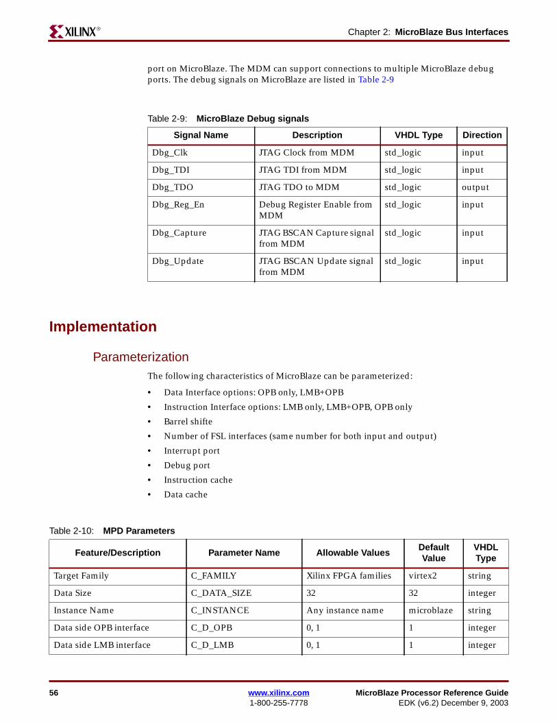
56 www.xilinx.com MicroBlaze Processor Reference Guide1-800-255-7778 EDK (v6.2) December 9, 2003
Chapter 2: MicroBlaze Bus InterfacesR
port on MicroBlaze. The MDM can support connections to multiple MicroBlaze debugports. The debug signals on MicroBlaze are listed in Table 2-9
Implementation
ParameterizationThe following characteristics of MicroBlaze can be parameterized:
• Data Interface options: OPB only, LMB+OPB
• Instruction Interface options: LMB only, LMB+OPB, OPB only
• Barrel shifte
• Number of FSL interfaces (same number for both input and output)
• Interrupt port
• Debug port
• Instruction cache
• Data cache
Table 2-9: MicroBlaze Debug signals
Signal Name Description VHDL Type Direction
Dbg_Clk JTAG Clock from MDM std_logic input
Dbg_TDI JTAG TDI from MDM std_logic input
Dbg_TDO JTAG TDO to MDM std_logic output
Dbg_Reg_En Debug Register Enable fromMDM
std_logic input
Dbg_Capture JTAG BSCAN Capture signalfrom MDM
std_logic input
Dbg_Update JTAG BSCAN Update signalfrom MDM
std_logic input
Table 2-10: MPD Parameters
Feature/Description Parameter Name Allowable ValuesDefaultValue
VHDLType
Target Family C_FAMILY Xilinx FPGA families virtex2 string
Data Size C_DATA_SIZE 32 32 integer
Instance Name C_INSTANCE Any instance name microblaze string
Data side OPB interface C_D_OPB 0, 1 1 integer
Data side LMB interface C_D_LMB 0, 1 1 integer
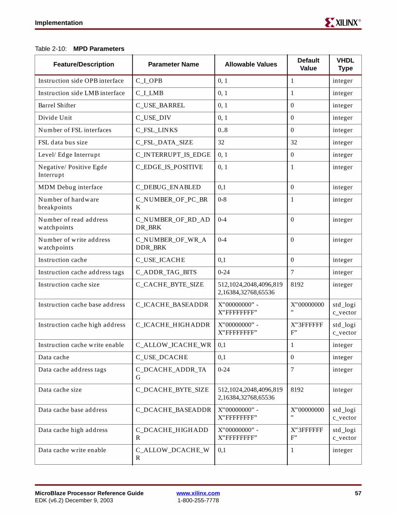
MicroBlaze Processor Reference Guide www.xilinx.com 57EDK (v6.2) December 9, 2003 1-800-255-7778
ImplementationR
Instruction side OPB interface C_I_OPB 0, 1 1 integer
Instruction side LMB interface C_I_LMB 0, 1 1 integer
Barrel Shifter C_USE_BARREL 0, 1 0 integer
Divide Unit C_USE_DIV 0, 1 0 integer
Number of FSL interfaces C_FSL_LINKS 0..8 0 integer
FSL data bus size C_FSL_DATA_SIZE 32 32 integer
Level/Edge Interrupt C_INTERRUPT_IS_EDGE 0, 1 0 integer
Negative/Positive EgdeInterrupt
C_EDGE_IS_POSITIVE 0, 1 1 integer
MDM Debug interface C_DEBUG_ENABLED 0,1 0 integer
Number of hardwarebreakpoints
C_NUMBER_OF_PC_BRK
0-8 1 integer
Number of read addresswatchpoints
C_NUMBER_OF_RD_ADDR_BRK
0-4 0 integer
Number of write addresswatchpoints
C_NUMBER_OF_WR_ADDR_BRK
0-4 0 integer
Instruction cache C_USE_ICACHE 0,1 0 integer
Instruction cache address tags C_ADDR_TAG_BITS 0-24 7 integer
Instruction cache size C_CACHE_BYTE_SIZE 512,1024,2048,4096,8192,16384,32768,65536
8192 integer
Instruction cache base address C_ICACHE_BASEADDR X”00000000” -X”FFFFFFFF”
X”00000000”
std_logic_vector
Instruction cache high address C_ICACHE_HIGHADDR X”00000000” -X”FFFFFFFF”
X”3FFFFFFF”
std_logic_vector
Instruction cache write enable C_ALLOW_ICACHE_WR 0,1 1 integer
Data cache C_USE_DCACHE 0,1 0 integer
Data cache address tags C_DCACHE_ADDR_TAG
0-24 7 integer
Data cache size C_DCACHE_BYTE_SIZE 512,1024,2048,4096,8192,16384,32768,65536
8192 integer
Data cache base address C_DCACHE_BASEADDR X”00000000” -X”FFFFFFFF”
X”00000000”
std_logic_vector
Data cache high address C_DCACHE_HIGHADDR
X”00000000” -X”FFFFFFFF”
X”3FFFFFFF”
std_logic_vector
Data cache write enable C_ALLOW_DCACHE_WR
0,1 1 integer
Table 2-10: MPD Parameters
Feature/Description Parameter Name Allowable ValuesDefaultValue
VHDLType

58 www.xilinx.com MicroBlaze Processor Reference Guide1-800-255-7778 EDK (v6.2) December 9, 2003
Chapter 2: MicroBlaze Bus InterfacesR
MicroBlaze Processor Reference Guide www.xilinx.com 59EDK (v6.2) December 9, 2003 1-800-255-7778
R
Chapter 3
MicroBlaze Endianness
This chapter describes big-endian and little-endian data objects and how to use little-endian data with the big-endian MicroBlaze soft processor. This chapter includes thefollowing sections
• “Definitions”
• “Bit Naming Conventions”
• “Data Types and Endianness”
• “VHDL Example”
DefinitionsData are stored or retrieved in memory, in byte, half word, word, or double word units.Endianness refers to the order in which data are stored and retrieved. Little-endianspecifies that the least significant byte is assigned the lowest byte address. Big-endianspecifies that the most significant byte is assigned the lowest byte address.
Note Endianness does not affect single byte data.
Bit Naming ConventionsThe MicroBlaze architecture uses a bus and register bit naming convention in which themost significant bit (MSB) name incorporates zero (‘0’). As the significance of the bitsdecreases across the bus, the number in the name increases linearly so that a 32-bit vectorhas a least significant bit (LSB) name equal to 31. Other Xilinx interfaces such as the PCICore use the opposite convention in which a name with a ‘0’ represents the LSB vectorposition.
Data Types and EndiannessHardware supported data types for MicroBlaze are word, half word, and byte. The dataorganization for each type is shown in the following tables.
Table 3-1: Word Data Type
Byte address n n+1 n+2 n+3
Byte label 0 1 2 3
Bytesignificance
MSByte
LSByte
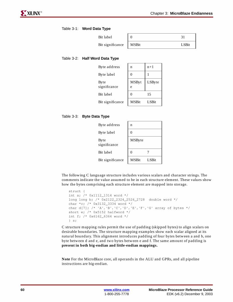
60 www.xilinx.com MicroBlaze Processor Reference Guide1-800-255-7778 EDK (v6.2) December 9, 2003
Chapter 3: MicroBlaze EndiannessR
The following C language structure includes various scalars and character strings. Thecomments indicate the value assumed to be in each structure element. These values showhow the bytes comprising each structure element are mapped into storage.
struct {int a; /* 0x1112_1314 word */long long b; /* 0x2122_2324_2526_2728 double word */char *c; /* 0x3132_3334 word */char d[7]; /* 'A','B','C','D','E','F','G' array of bytes */short e; /* 0x5152 halfword */int f; /* 0x6162_6364 word */} s;
C structure mapping rules permit the use of padding (skipped bytes) to align scalars ondesirable boundaries. The structure mapping examples show each scalar aligned at itsnatural boundary. This alignment introduces padding of four bytes between a and b, onebyte between d and e, and two bytes between e and f. The same amount of padding ispresent in both big-endian and little-endian mappings.
Note For the MicroBlaze core, all operands in the ALU and GPRs, and all pipelineinstructions are big-endian.
Bit label 0 31
Bit significance MSBit LSBit
Table 3-2: Half Word Data Type
Byte address n n+1
Byte label 0 1
Bytesignificance
MSByte
LSByte
Bit label 0 15
Bit significance MSBit LSBit
Table 3-3: Byte Data Type
Byte address n
Byte label 0
Bytesignificance
MSByte
Bit label 0 7
Bit significance MSBit LSBit
Table 3-1: Word Data Type
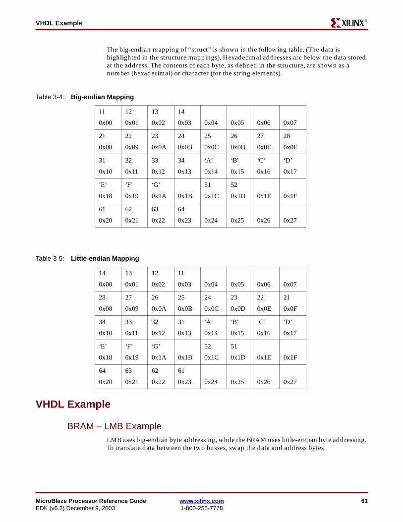
MicroBlaze Processor Reference Guide www.xilinx.com 61EDK (v6.2) December 9, 2003 1-800-255-7778
VHDL ExampleR
The big-endian mapping of “struct” is shown in the following table. (The data ishighlighted in the structure mappings). Hexadecimal addresses are below the data storedat the address. The contents of each byte, as defined in the structure, are shown as anumber (hexadecimal) or character (for the string elements).
VHDL Example
BRAM – LMB ExampleLMB uses big-endian byte addressing, while the BRAM uses little-endian byte addressing.To translate data between the two busses, swap the data and address bytes.
Table 3-4: Big-endian Mapping
11
0x00
12
0x01
13
0x02
14
0x03 0x04 0x05 0x06 0x07
21
0x08
22
0x09
23
0x0A
24
0x0B
25
0x0C
26
0x0D
27
0x0E
28
0x0F
31
0x10
32
0x11
33
0x12
34
0x13
‘A’
0x14
‘B’
0x15
‘C’
0x16
‘D’
0x17
‘E’
0x18
‘F’
0x19
‘G’
0x1A 0x1B
51
0x1C
52
0x1D 0x1E 0x1F
61
0x20
62
0x21
63
0x22
64
0x23 0x24 0x25 0x26 0x27
Table 3-5: Little-endian Mapping
14
0x00
13
0x01
12
0x02
11
0x03 0x04 0x05 0x06 0x07
28
0x08
27
0x09
26
0x0A
25
0x0B
24
0x0C
23
0x0D
22
0x0E
21
0x0F
34
0x10
33
0x11
32
0x12
31
0x13
‘A’
0x14
‘B’
0x15
‘C’
0x16
‘D’
0x17
‘E’
0x18
‘F’
0x19
‘G’
0x1A 0x1B
52
0x1C
51
0x1D 0x1E 0x1F
64
0x20
63
0x21
62
0x22
61
0x23 0x24 0x25 0x26 0x27
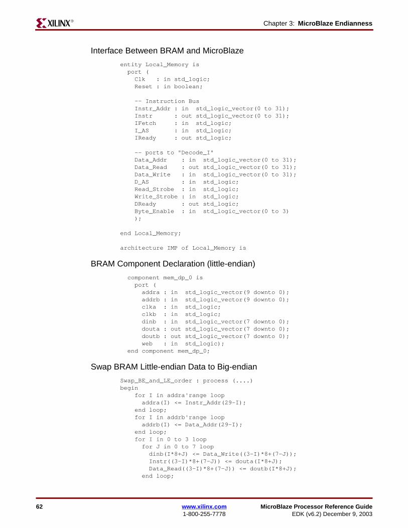
62 www.xilinx.com MicroBlaze Processor Reference Guide1-800-255-7778 EDK (v6.2) December 9, 2003
Chapter 3: MicroBlaze EndiannessR
Interface Between BRAM and MicroBlaze
entity Local_Memory is port ( Clk : in std_logic; Reset : in boolean;
-- Instruction Bus Instr_Addr : in std_logic_vector(0 to 31); Instr : out std_logic_vector(0 to 31); IFetch : in std_logic; I_AS : in std_logic; IReady : out std_logic;
-- ports to "Decode_I" Data_Addr : in std_logic_vector(0 to 31); Data_Read : out std_logic_vector(0 to 31); Data_Write : in std_logic_vector(0 to 31); D_AS : in std_logic; Read_Strobe : in std_logic; Write_Strobe : in std_logic; DReady : out std_logic; Byte_Enable : in std_logic_vector(0 to 3) );
end Local_Memory;
architecture IMP of Local_Memory is
BRAM Component Declaration (little-endian)
component mem_dp_0 is port ( addra : in std_logic_vector(9 downto 0); addrb : in std_logic_vector(9 downto 0); clka : in std_logic; clkb : in std_logic; dinb : in std_logic_vector(7 downto 0); douta : out std_logic_vector(7 downto 0); doutb : out std_logic_vector(7 downto 0); web : in std_logic); end component mem_dp_0;
Swap BRAM Little-endian Data to Big-endian
Swap_BE_and_LE_order : process (....)begin for I in addra'range loop addra(I) <= Instr_Addr(29-I); end loop; for I in addrb'range loop addrb(I) <= Data_Addr(29-I); end loop; for I in 0 to 3 loop for J in 0 to 7 loop dinb(I*8+J) <= Data_Write((3-I)*8+(7-J)); Instr((3-I)*8+(7-J)) <= douta(I*8+J); Data_Read((3-I)*8+(7-J)) <= doutb(I*8+J); end loop;
MicroBlaze Processor Reference Guide www.xilinx.com 63EDK (v6.2) December 9, 2003 1-800-255-7778
VHDL ExampleR
end loop; end process Swap_BE_and_LE_order;
BRAM Instantiation
mem_dp_0_I : mem_dp_0port map (addra=>addra, --[IN std_logic_VECTOR(9 downto 0)]addrb=>addrb, --[IN std_logic_VECTOR(9 downto 0)]clka=>Clk, --[IN std_logic]clkb=>Clk, --[IN std_logic]dinb=>dinb(31 downto 24)--[IN std_logic_VECTOR(7 downto 0)]douta=>douta(31 downto 24), --[OUT std_logic_VECTOR(7 downto 0)]doutb => doutb(31 downto 24), --[OUT std_logic_VECTOR(7 downto 0)]web=>we(0)); --[IN std_logic]
BRAM – OPB ExampleOPB uses big-endian byte addressing, while the BRAM uses little-endian byte addressing.To translate data between the two buses, swap the data and address bytes.
Interface Between BRAM and MicroBlaze
library IEEE;use IEEE.std_logic_1164.all;
entity OPB_BRAM is generic ( C_BASEADDR : std_logic_vector(0 to 31) := X"B000_0000"; C_NO_BRAMS : natural := 4; -- Can be 4,8,16,32 only C_VIRTEXII : boolean := true ); port ( -- Global signals OPB_Clk : in std_logic; OPB_Rst : in std_logic;
-- OPB signals OPB_ABus : in std_logic_vector(0 to 31); OPB_BE : in std_logic_vector(0 to 3); OPB_RNW : in std_logic; OPB_select : in std_logic; OPB_seqAddr : in std_logic; OPB_DBus : in std_logic_vector(0 to 31);
OPB_BRAM_DBus : out std_logic_vector(0 to 31); OPB_BRAM_errAck : out std_logic; OPB_BRAM_retry : out std_logic; OPB_BRAM_toutSup : out std_logic; OPB_BRAM_xferAck : out std_logic;
-- OPB_BRAM signals (other port) BRAM_Clk : in std_logic; BRAM_Addr : in std_logic_vector(0 to 31); BRAM_WE : in std_logic_vector(0 to 3); BRAM_Write_Data : in std_logic_vector(0 to 31); BRAM_Read_Data : out std_logic_vector(0 to 31) );
64 www.xilinx.com MicroBlaze Processor Reference Guide1-800-255-7778 EDK (v6.2) December 9, 2003
Chapter 3: MicroBlaze EndiannessR
end entity OPB_BRAM;
architecture IMP of OPB_BRAM is
BRAM Component Declaration (little-endian)
component RAMB16_S9_S9 port ( DIA : in std_logic_vector (7 downto 0); DIB : in std_logic_vector (7 downto 0); DIPA : in std_logic_vector (0 downto 0); DIPB : in std_logic_vector (0 downto 0); ENA : in std_ulogic; ENB : in std_ulogic; WEA : in std_ulogic; WEB : in std_ulogic; SSRA : in std_ulogic; SSRB : in std_ulogic; CLKA : in std_ulogic; CLKB : in std_ulogic; ADDRA : in std_logic_vector (10 downto 0); ADDRB : in std_logic_vector (10 downto 0); DOA : out std_logic_vector (7 downto 0); DOB : out std_logic_vector (7 downto 0); DOPA : out std_logic_vector (0 downto 0); DOPB : out std_logic_vector (0 downto 0) ); end component;Swap BRAM Little-endian Data to Big-endian BE_to_LE : for I in 0 to 31 generate opb_dbus_le(I ) <= OPB_DBus(31-I); bram_write_data_le(I) <= BRAM_Write_Data(31-I); BRAM_Read_Data(I) <= bram_Read_Data_LE(31-I); opb_ABus_LE(I) <= OPB_ABus(31-I); bram_Addr_LE(I) <= BRAM_Addr(31-I); end generate BE_to_LE;
BRAM Instantiation
All_Brams : for I in 0 to C_NO_BRAMS-1 generate
By_8 : if (C_NO_BRAMS = 4) generate
RAMB16_S9_S9_I : RAMB16_S9_S9port map (DIA => opb_DBUS_LE(((I+1)*8-1) downto I*8), --[in std_logic_vector(7downto 0)]DIB =>bram_Write_Data_LE(((I+1)*8)-1 downto I*8), --[instd_logic_vector (downto 0)]DIPA => null_1, -- [in std_logic_vector (7 downto 0)]DIPB => null_1, -- [in std_logic_vector (7 downto 0)]ENA => '1', -- [in std_ulogic]ENB => '1', -- [in std_ulogic]WEA => opb_WE(I), -- [in std_ulogic]WEB => BRAM_WE(I), -- [in std_ulogic]SSRA => '0', -- [in std_ulogic]SSRB => '0', -- [in std_ulogic]CLKA => OPB_Clk, -- [in std_ulogic]CLKB => BRAM_Clk, -- [in std_ulogic]
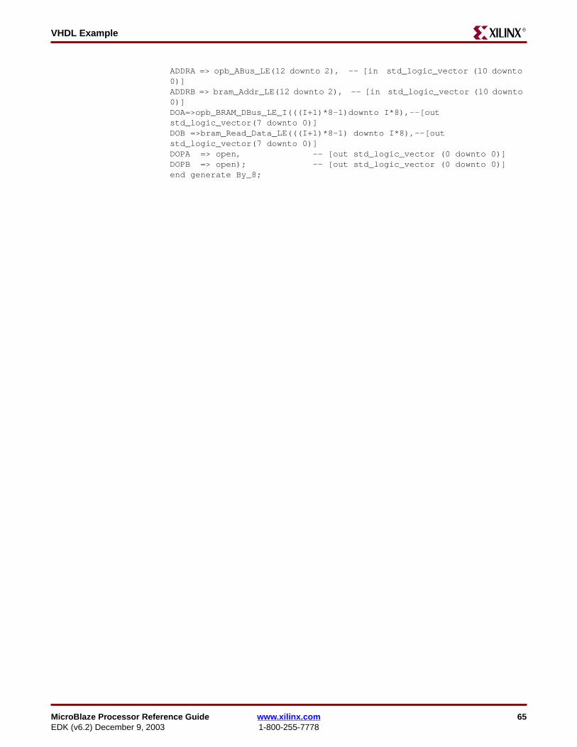
MicroBlaze Processor Reference Guide www.xilinx.com 65EDK (v6.2) December 9, 2003 1-800-255-7778
VHDL ExampleR
ADDRA => opb_ABus_LE(12 downto 2), -- [in std_logic_vector (10 downto0)]ADDRB => bram_Addr_LE(12 downto 2), -- [in std_logic_vector (10 downto0)]DOA=>opb_BRAM_DBus_LE_I(((I+1)*8-1)downto I*8),--[outstd_logic_vector(7 downto 0)]DOB =>bram_Read_Data_LE(((I+1)*8-1) downto I*8),--[outstd_logic_vector(7 downto 0)]DOPA => open, -- [out std_logic_vector (0 downto 0)]DOPB => open); -- [out std_logic_vector (0 downto 0)]end generate By_8;

66 www.xilinx.com MicroBlaze Processor Reference Guide1-800-255-7778 EDK (v6.2) December 9, 2003
Chapter 3: MicroBlaze EndiannessR
MicroBlaze Processor Reference Guide www.xilinx.com 67EDK (v6.2) December 9, 2003 1-800-255-7778
R
Chapter 4
MicroBlaze Application BinaryInterface
ScopeThis document describes MicroBlaze Application Binary Interface (ABI), which isimportant for developing software in assembly language for the soft processor. TheMicroBlaze GNU compiler follows the conventions described in this document. Hence anycode written by assembly programmers should also follow the same conventions to becompatible with the compiler generated code. Interrupt and Exception handling is alsoexplained briefly in the document.
Data TypesThe data types used by MicroBlaze assembly programs are shown in Table 4-1. Data typessuch as data8, data16, and data32 are used in place of the usual byte, halfword, and word.
Register Usage ConventionsThe register usage convention for MicroBlaze is given in Table 4-2.
Table 4-1: Data types in MicroBlaze assembly programs
MicroBlaze data types(for assembly programs)
CorrespondingANSI C data types
Size (bytes)
data8 char 1
data16 short 2
data32 int 4
data32 long int 4
data32 enum 4
data16/data32 pointera
a.Pointers to small data areas, which can be accessed by global pointers aredata16.
2/4
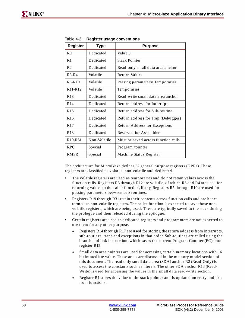
68 www.xilinx.com MicroBlaze Processor Reference Guide1-800-255-7778 EDK (v6.2) December 9, 2003
Chapter 4: MicroBlaze Application Binary InterfaceR
The architecture for MicroBlaze defines 32 general purpose registers (GPRs). Theseregisters are classified as volatile, non-volatile and dedicated.
• The volatile registers are used as temporaries and do not retain values across thefunction calls. Registers R3 through R12 are volatile, of which R3 and R4 are used forreturning values to the caller function, if any. Registers R5 through R10 are used forpassing parameters between sub-routines.
• Registers R19 through R31 retain their contents across function calls and are hencetermed as non-volatile registers. The callee function is expected to save those non-volatile registers, which are being used. These are typically saved to the stack duringthe prologue and then reloaded during the epilogue.
• Certain registers are used as dedicated registers and programmers are not expected touse them for any other purpose.
♦ Registers R14 through R17 are used for storing the return address from interrupts,sub-routines, traps and exceptions in that order. Sub-routines are called using thebranch and link instruction, which saves the current Program Counter (PC) ontoregister R15.
♦ Small data area pointers are used for accessing certain memory locations with 16bit immediate value. These areas are discussed in the memory model section ofthis document. The read only small data area (SDA) anchor R2 (Read-Only) isused to access the constants such as literals. The other SDA anchor R13 (Read-Write) is used for accessing the values in the small data read-write section.
♦ Register R1 stores the value of the stack pointer and is updated on entry and exitfrom functions.
Table 4-2: Register usage conventions
Register Type Purpose
R0 Dedicated Value 0
R1 Dedicated Stack Pointer
R2 Dedicated Read-only small data area anchor
R3-R4 Volatile Return Values
R5-R10 Volatile Passing parameters/Temporaries
R11-R12 Volatile Temporaries
R13 Dedicated Read-write small data area anchor
R14 Dedicated Return address for Interrupt
R15 Dedicated Return address for Sub-routine
R16 Dedicated Return address for Trap (Debugger)
R17 Dedicated Return Address for Exceptions
R18 Dedicated Reserved for Assembler
R19-R31 Non-Volatile Must be saved across function calls
RPC Special Program counter
RMSR Special Machine Status Register
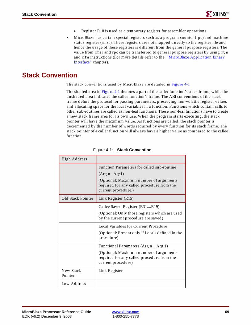
MicroBlaze Processor Reference Guide www.xilinx.com 69EDK (v6.2) December 9, 2003 1-800-255-7778
Stack ConventionR
♦ Register R18 is used as a temporary register for assembler operations.
• MicroBlaze has certain special registers such as a program counter (rpc) and machinestatus register (rmsr). These registers are not mapped directly to the register file andhence the usage of these registers is different from the general purpose registers. Thevalue from rmsr and rpc can be transferred to general purpose registers by using mtsand mfs instructions (For more details refer to the “MicroBlaze Application BinaryInterface” chapter).
Stack ConventionThe stack conventions used by MicroBlaze are detailed in Figure 4-1
The shaded area in Figure 4-1 denotes a part of the caller function’s stack frame, while theunshaded area indicates the callee function’s frame. The ABI conventions of the stackframe define the protocol for passing parameters, preserving non-volatile register valuesand allocating space for the local variables in a function. Functions which contain calls toother sub-routines are called as non-leaf functions, These non-leaf functions have to createa new stack frame area for its own use. When the program starts executing, the stackpointer will have the maximum value. As functions are called, the stack pointer isdecremented by the number of words required by every function for its stack frame. Thestack pointer of a caller function will always have a higher value as compared to the calleefunction.
Figure 4-1: Stack Convention
High Address
Function Parameters for called sub-routine
(Arg n ..Arg1)
(Optional: Maximum number of argumentsrequired for any called procedure from thecurrent procedure.)
Old Stack Pointer Link Register (R15)
Callee Saved Register (R31....R19)
(Optional: Only those registers which are usedby the current procedure are saved)
Local Variables for Current Procedure
(Optional: Present only if Locals defined in theprocedure)
Functional Parameters (Arg n .. Arg 1)
(Optional: Maximum number of argumentsrequired for any called procedure from thecurrent procedure)
New StackPointer
Link Register
Low Address
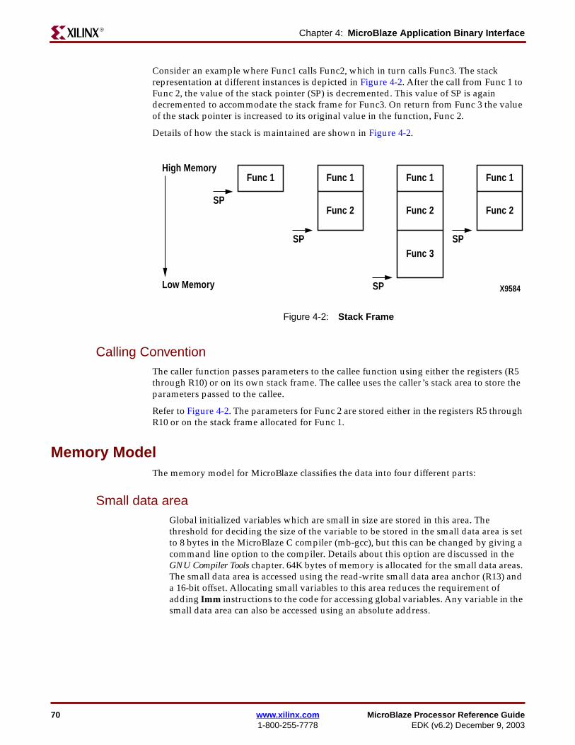
70 www.xilinx.com MicroBlaze Processor Reference Guide1-800-255-7778 EDK (v6.2) December 9, 2003
Chapter 4: MicroBlaze Application Binary InterfaceR
Consider an example where Func1 calls Func2, which in turn calls Func3. The stackrepresentation at different instances is depicted in Figure 4-2. After the call from Func 1 toFunc 2, the value of the stack pointer (SP) is decremented. This value of SP is againdecremented to accommodate the stack frame for Func3. On return from Func 3 the valueof the stack pointer is increased to its original value in the function, Func 2.
Details of how the stack is maintained are shown in Figure 4-2.
Figure 4-2: Stack Frame
Calling ConventionThe caller function passes parameters to the callee function using either the registers (R5through R10) or on its own stack frame. The callee uses the caller’s stack area to store theparameters passed to the callee.
Refer to Figure 4-2. The parameters for Func 2 are stored either in the registers R5 throughR10 or on the stack frame allocated for Func 1.
Memory ModelThe memory model for MicroBlaze classifies the data into four different parts:
Small data areaGlobal initialized variables which are small in size are stored in this area. Thethreshold for deciding the size of the variable to be stored in the small data area is setto 8 bytes in the MicroBlaze C compiler (mb-gcc), but this can be changed by giving acommand line option to the compiler. Details about this option are discussed in theGNU Compiler Tools chapter. 64K bytes of memory is allocated for the small data areas.The small data area is accessed using the read-write small data area anchor (R13) anda 16-bit offset. Allocating small variables to this area reduces the requirement ofadding Imm instructions to the code for accessing global variables. Any variable in thesmall data area can also be accessed using an absolute address.
X9584
High Memory
Low Memory
SP
Func 1
SP
Func 1
Func 2
SP
Func 1
Func 2
Func 3SP
Func 1
Func 2
MicroBlaze Processor Reference Guide www.xilinx.com 71EDK (v6.2) December 9, 2003 1-800-255-7778
Interrupt and Exception HandlingR
Data areaComparatively large initialized variables are allocated to the data area, which caneither be accessed using the read-write SDA anchor R13 or using the absolute address,depending on the command line option given to the compiler.
Common un-initialized areaUn-initialized global variables are allocated to the comm area and can be accessedeither using the absolute address or using the read-write small data area anchor R13.
Literals or constantsConstants are placed into the read-only small data area and are accessed using theread-only small data area anchor R2.
The compiler generates appropriate global pointers to act as base pointers. The actualvalues of the SDA anchors are decided by the linker, in the final linking stages. For moreinformation on the various sections of the memory please refer to the Address Managementchapter. The compiler generates appropriate sections, depending on the command lineoptions. Please refer to the GNU Compiler Tools chapter for more information about theseoptions.
Interrupt and Exception HandlingMicroBlaze assumes certain address locations for handling interrupts and exceptions asindicated in Table 4-3. When the device is powered ON or on a reset, execution starts at0x0. If an exception occurs, MicroBlaze jumps to address location 0x8, while in case of aninterrupt, the control is passed to address location 0x10. At these locations, code is writtento jump to the appropriate handlers.
The code expected at these locations is as shown in Figure 4-3. In case of programscompiled without the -xl-mode-xmdstub compiler option, the crt0.o initialization file ispassed by the mb-gcc compiler to the mb-ld linker for linking. This file sets the appropriateaddresses of the exception handlers.
In case of programs compiled with the -xl-mode-xmdstub compiler option, the crt1.oinitialization file is linked to the output program. This program has to be run with thexmdstub already loaded in the memory at address location 0x0. Hence at run-time, theinitialization code in crt1.o writes the appropriate instructions to location 0x8 through 0x14depending on the address of the exception and interrupt handlers.
Table 4-3: Interrupt and Exception Handling
On Hardware jumps to Software Labels
Start / Reset 0x0 _start
Exception 0x8 _exception_handler
Interrupt 0x10 _interrupt_handler

72 www.xilinx.com MicroBlaze Processor Reference Guide1-800-255-7778 EDK (v6.2) December 9, 2003
Chapter 4: MicroBlaze Application Binary InterfaceR
Figure 4-3: Code for passing control to exception and interrupt handlers
MicroBlaze allows exception and interrupt handler routines to be located at any addresslocation addressable using 32 bits. The exception handler code starts with the label_exception_handler, while the interrupt handler code starts with the label_interrupt_handler.
In the current MicroBlaze system, there are dummy routines for interrupt or exceptionhandling, which you can change. In order to override these routines and link yourinterrupt and exception handlers, you must define the interrupt handler code with anattribute interrupt_handler. For more details about the use and syntax of the interrupthandler attribute, please refer to the GNU Compiler Tools chapter.
0x00: bri _start10x04: nop0x08: imm high bits of address (exception handler)0x0c: bri _exception_handler0x10: imm high bits of address (interrupt handler)0x14: bri _interrupt_handler
MicroBlaze Processor Reference Guide www.xilinx.com 73EDK (v6.2) December 9, 2003 1-800-255-7778
R
Chapter 5
MicroBlaze Instruction Set Architecture
SummaryThis chapter provides a detailed guide to the Instruction Set Architecture of MicroBlaze™.
NotationThe symbols used throughout this document are defined in Table 1.
Table 1: Symbol notation
Symbol Meaning
+ Add
- Subtract
× Multiply
∧ Bitwise logical AND
∨ Bitwise logical OR
⊕ Bitwise logical XOR
x Bitwise logical complement of x
← Assignment
>> Right shift
<< Left shift
rx Register x
x[i] Bit i in register x
x[i:j] Bits i through j in register x
= Equal comparison
≠ Not equal comparison
> Greater than comparison
>= Greater than or equal comparison
< Less than comparison
<= Less than or equal comparison
sext(x) Sign-extend x
74 www.xilinx.com MicroBlaze Processor Reference Guide1-800-255-7778 EDK (v6.2) December 9, 2003
Chapter 5: MicroBlaze Instruction Set ArchitectureR
FormatsMicroBlaze uses two instruction formats: Type A and Type B.
Type A
Type A is used for register-register instructions. It contains the opcode, one destination andtwo source registers.
Type B
Type B is used for register-immediate instructions. It contains the opcode, one destinationand one source registers, and a source 16-bit immediate value.
InstructionsMicroBlaze instructions are described next. Instructions are listed in alphabetical order. Foreach instruction Xilinx provides the mnemonic, encoding, a description of it, pseudocodeof its semantics, and a list of registers that it modifies.
Mem(x) Memory location at address x
FSLx FSL interface x
LSW(x) Least Significant Word of x
Table 1: Symbol notation
Symbol Meaning
Opcode Destination Reg Source Reg A Source Reg B 0 0 0 0 0 0 0 0 0 0 0
0 6 11 16 21 31
Opcode Destination Reg Source Reg A Immediate Value
0 6 11 16 31
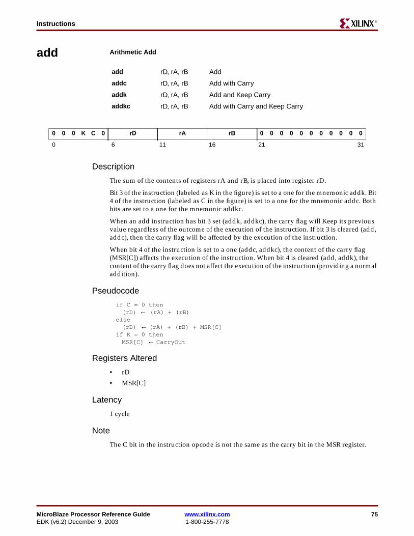
MicroBlaze Processor Reference Guide www.xilinx.com 75EDK (v6.2) December 9, 2003 1-800-255-7778
InstructionsR
add Arithmetic Add
Description
The sum of the contents of registers rA and rB, is placed into register rD.
Bit 3 of the instruction (labeled as K in the figure) is set to a one for the mnemonic addk. Bit4 of the instruction (labeled as C in the figure) is set to a one for the mnemonic addc. Bothbits are set to a one for the mnemonic addkc.
When an add instruction has bit 3 set (addk, addkc), the carry flag will Keep its previousvalue regardless of the outcome of the execution of the instruction. If bit 3 is cleared (add,addc), then the carry flag will be affected by the execution of the instruction.
When bit 4 of the instruction is set to a one (addc, addkc), the content of the carry flag(MSR[C]) affects the execution of the instruction. When bit 4 is cleared (add, addk), thecontent of the carry flag does not affect the execution of the instruction (providing a normaladdition).
Pseudocode
if C = 0 then(rD) ← (rA) + (rB)
else(rD) ← (rA) + (rB) + MSR[C]
if K = 0 thenMSR[C] ← CarryOut
Registers Altered
• rD
• MSR[C]
Latency
1 cycle
Note
The C bit in the instruction opcode is not the same as the carry bit in the MSR register.
add rD, rA, rB Add
addc rD, rA, rB Add with Carry
addk rD, rA, rB Add and Keep Carry
addkc rD, rA, rB Add with Carry and Keep Carry
0 0 0 K C 0 rD rA rB 0 0 0 0 0 0 0 0 0 0 0
0 6 11 16 21 31
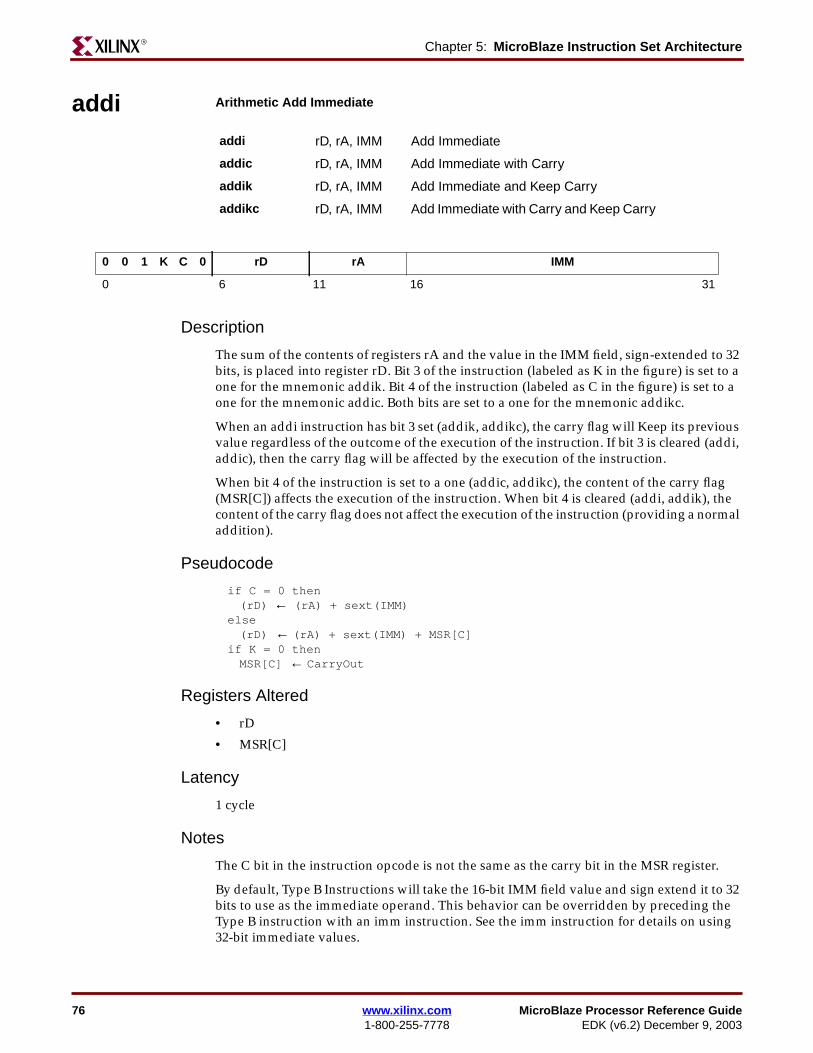
76 www.xilinx.com MicroBlaze Processor Reference Guide1-800-255-7778 EDK (v6.2) December 9, 2003
Chapter 5: MicroBlaze Instruction Set ArchitectureR
addi Arithmetic Add Immediate
Description
The sum of the contents of registers rA and the value in the IMM field, sign-extended to 32bits, is placed into register rD. Bit 3 of the instruction (labeled as K in the figure) is set to aone for the mnemonic addik. Bit 4 of the instruction (labeled as C in the figure) is set to aone for the mnemonic addic. Both bits are set to a one for the mnemonic addikc.
When an addi instruction has bit 3 set (addik, addikc), the carry flag will Keep its previousvalue regardless of the outcome of the execution of the instruction. If bit 3 is cleared (addi,addic), then the carry flag will be affected by the execution of the instruction.
When bit 4 of the instruction is set to a one (addic, addikc), the content of the carry flag(MSR[C]) affects the execution of the instruction. When bit 4 is cleared (addi, addik), thecontent of the carry flag does not affect the execution of the instruction (providing a normaladdition).
Pseudocode
if C = 0 then(rD) ← (rA) + sext(IMM)
else(rD) ← (rA) + sext(IMM) + MSR[C]
if K = 0 thenMSR[C] ← CarryOut
Registers Altered
• rD
• MSR[C]
Latency
1 cycle
Notes
The C bit in the instruction opcode is not the same as the carry bit in the MSR register.
By default, Type B Instructions will take the 16-bit IMM field value and sign extend it to 32bits to use as the immediate operand. This behavior can be overridden by preceding theType B instruction with an imm instruction. See the imm instruction for details on using32-bit immediate values.
addi rD, rA, IMM Add Immediate
addic rD, rA, IMM Add Immediate with Carry
addik rD, rA, IMM Add Immediate and Keep Carry
addikc rD, rA, IMM Add Immediate with Carry and Keep Carry
0 0 1 K C 0 rD rA IMM
0 6 11 16 31
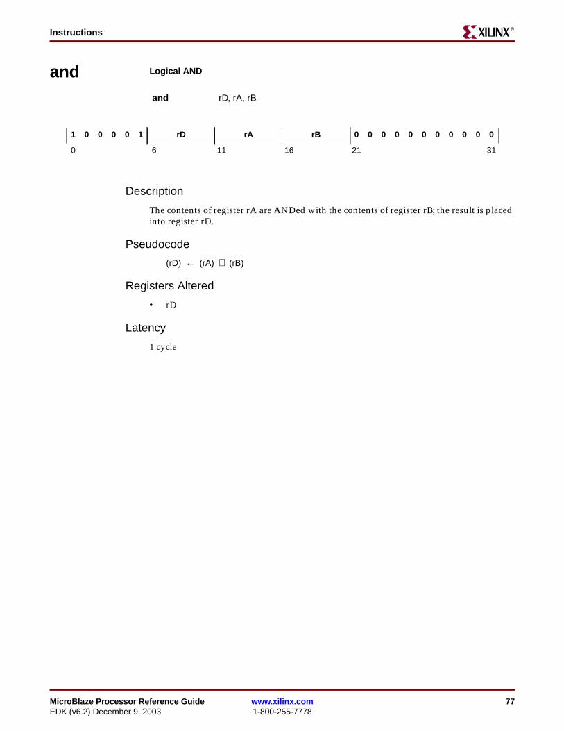
MicroBlaze Processor Reference Guide www.xilinx.com 77EDK (v6.2) December 9, 2003 1-800-255-7778
InstructionsR
and Logical AND
Description
The contents of register rA are ANDed with the contents of register rB; the result is placedinto register rD.
Pseudocode
(rD) ← (rA) ∧ (rB)
Registers Altered
• rD
Latency
1 cycle
and rD, rA, rB
1 0 0 0 0 1 rD rA rB 0 0 0 0 0 0 0 0 0 0 0
0 6 11 16 21 31
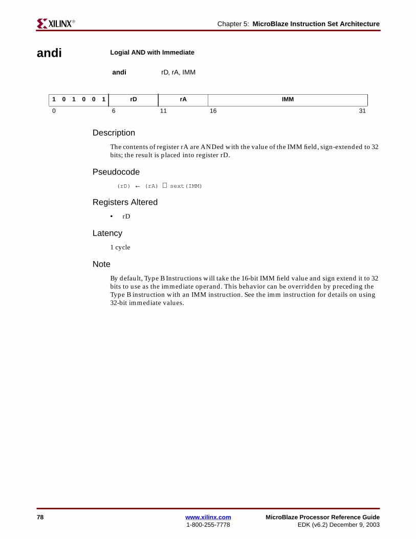
78 www.xilinx.com MicroBlaze Processor Reference Guide1-800-255-7778 EDK (v6.2) December 9, 2003
Chapter 5: MicroBlaze Instruction Set ArchitectureR
andi Logial AND with Immediate
Description
The contents of register rA are ANDed with the value of the IMM field, sign-extended to 32bits; the result is placed into register rD.
Pseudocode
(rD) ← (rA) ∧ sext(IMM)
Registers Altered
• rD
Latency
1 cycle
Note
By default, Type B Instructions will take the 16-bit IMM field value and sign extend it to 32bits to use as the immediate operand. This behavior can be overridden by preceding theType B instruction with an IMM instruction. See the imm instruction for details on using32-bit immediate values.
andi rD, rA, IMM
1 0 1 0 0 1 rD rA IMM
0 6 11 16 31
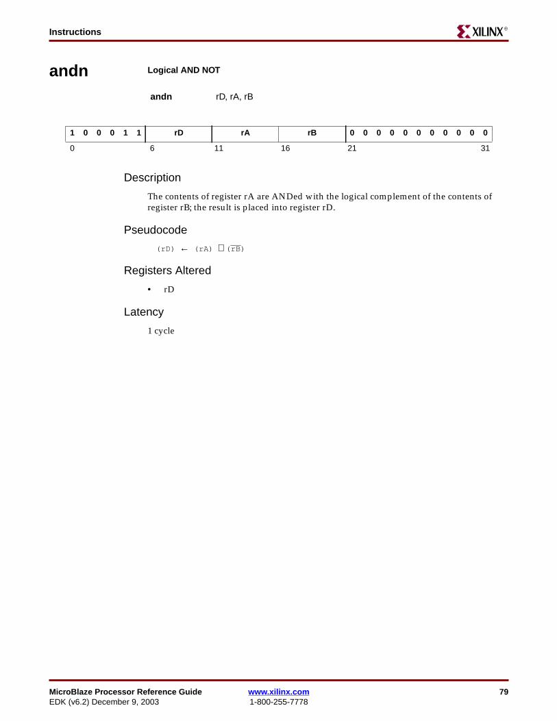
MicroBlaze Processor Reference Guide www.xilinx.com 79EDK (v6.2) December 9, 2003 1-800-255-7778
InstructionsR
andn Logical AND NOT
Description
The contents of register rA are ANDed with the logical complement of the contents ofregister rB; the result is placed into register rD.
Pseudocode
(rD) ← (rA) ∧ (rB)
Registers Altered
• rD
Latency
1 cycle
andn rD, rA, rB
1 0 0 0 1 1 rD rA rB 0 0 0 0 0 0 0 0 0 0 0
0 6 11 16 21 31
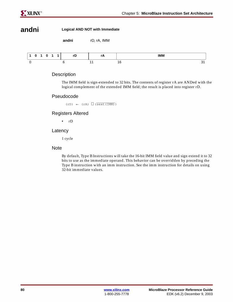
80 www.xilinx.com MicroBlaze Processor Reference Guide1-800-255-7778 EDK (v6.2) December 9, 2003
Chapter 5: MicroBlaze Instruction Set ArchitectureR
andni Logical AND NOT with Immediate
Description
The IMM field is sign-extended to 32 bits. The contents of register rA are ANDed with thelogical complement of the extended IMM field; the result is placed into register rD.
Pseudocode
(rD) ← (rA) ∧ (sext(IMM))
Registers Altered
• rD
Latency
1 cycle
Note
By default, Type B Instructions will take the 16-bit IMM field value and sign extend it to 32bits to use as the immediate operand. This behavior can be overridden by preceding theType B instruction with an imm instruction. See the imm instruction for details on using32-bit immediate values.
andni rD, rA, IMM
1 0 1 0 1 1 rD rA IMM
0 6 11 16 31

MicroBlaze Processor Reference Guide www.xilinx.com 81EDK (v6.2) December 9, 2003 1-800-255-7778
InstructionsR
beq Branch if Equal
Description
Branch if rA is equal to 0, to the instruction located in the offset value of rB. The target ofthe branch will be the instruction at address PC + rB.
The mnemonic beqd will set the D bit. The D bit determines whether there is a branchdelay slot or not. If the D bit is set, it means that there is a delay slot and the instructionfollowing the branch (i.e. in the branch delay slot) is allowed to complete execution beforeexecuting the target instruction. If the D bit is not set, it means that there is no delay slot, sothe instruction to be executed after the branch is the target instruction.
Pseudocode
If rA = 0 thenPC ← PC + rB
elsePC ← PC + 4
if D = 1 thenallow following instruction to complete execution
Registers Altered
• PC
Latency
1 cycle (if branch is not taken)
2 cycles (if branch is taken and the D bit is set)
3 cycles (if branch is taken and the D bit is not set)
beq rA, rB Branch if Equal
beqd rA, rB Branch if Equal with Delay
1 0 0 1 1 1 D 0 0 0 0 rA rB 0 0 0 0 0 0 0 0 0 0 0
0 6 11 16 21 31

82 www.xilinx.com MicroBlaze Processor Reference Guide1-800-255-7778 EDK (v6.2) December 9, 2003
Chapter 5: MicroBlaze Instruction Set ArchitectureR
beqi Branch Immediate if Equal
Description
Branch if rA is equal to 0, to the instruction located in the offset value of IMM. The targetof the branch will be the instruction at address PC + IMM.
The mnemonic beqid will set the D bit. The D bit determines whether there is a branchdelay slot or not. If the D bit is set, it means that there is a delay slot and the instructionfollowing the branch (i.e. in the branch delay slot) is allowed to complete execution beforeexecuting the target instruction. If the D bit is not set, it means that there is no delay slot, sothe instruction to be executed after the branch is the target instruction.
Pseudocode
If rA = 0 thenPC ← PC + sext(IMM)
elsePC ← PC + 4
if D = 1 thenallow following instruction to complete execution
Registers Altered
• PC
Latency
1 cycle (if branch is not taken)
2 cycles (if branch is taken and the D bit is set)
3 cycles (if branch is taken and the D bit is not set)
Note
By default, Type B Instructions will take the 16-bit IMM field value and sign extend it to 32bits to use as the immediate operand. This behavior can be overridden by preceding theType B instruction with an imm instruction. See the imm instruction for details on using32-bit immediate values.
beqi rA, IMM Branch Immediate if Equal
beqid rA, IMM Branch Immediate if Equal with Delay
1 0 1 1 1 1 D 0 0 0 0 rA IMM
0 6 11 16 31
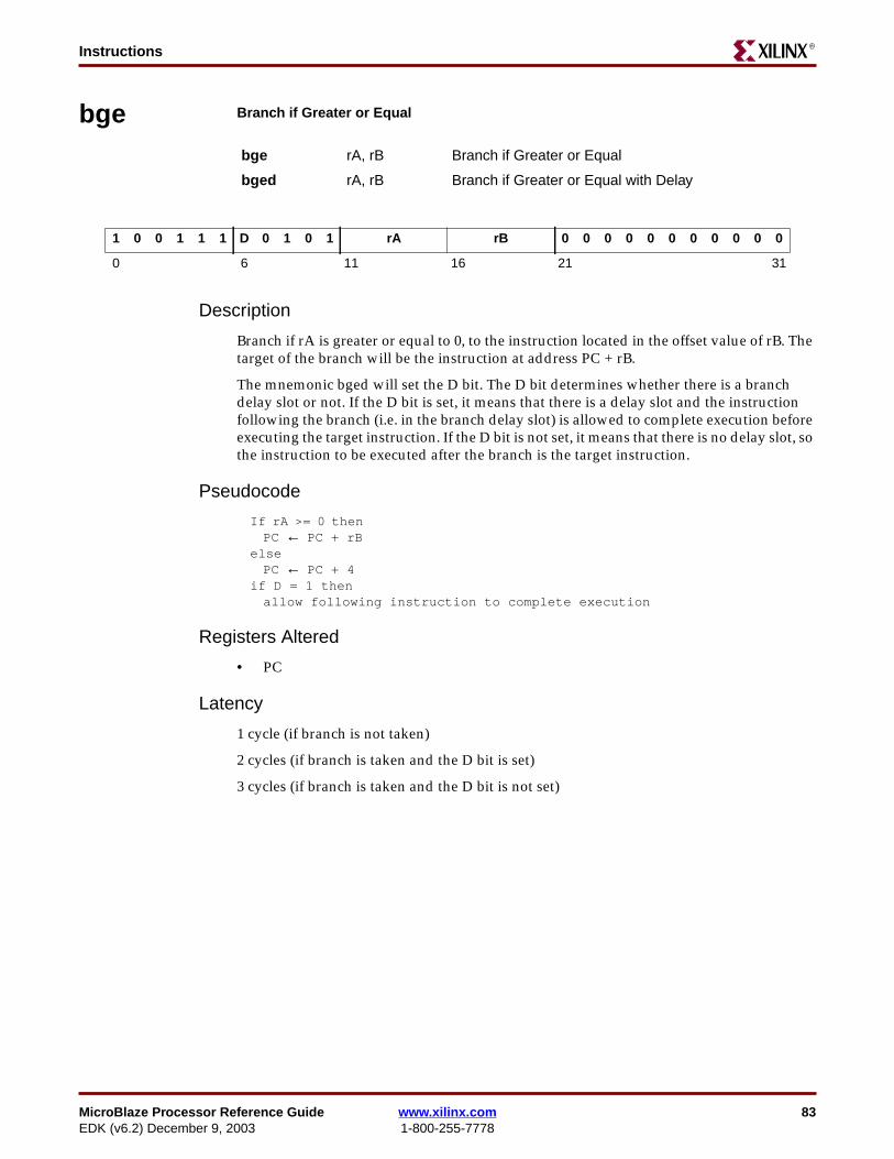
MicroBlaze Processor Reference Guide www.xilinx.com 83EDK (v6.2) December 9, 2003 1-800-255-7778
InstructionsR
bge Branch if Greater or Equal
Description
Branch if rA is greater or equal to 0, to the instruction located in the offset value of rB. Thetarget of the branch will be the instruction at address PC + rB.
The mnemonic bged will set the D bit. The D bit determines whether there is a branchdelay slot or not. If the D bit is set, it means that there is a delay slot and the instructionfollowing the branch (i.e. in the branch delay slot) is allowed to complete execution beforeexecuting the target instruction. If the D bit is not set, it means that there is no delay slot, sothe instruction to be executed after the branch is the target instruction.
Pseudocode
If rA >= 0 thenPC ← PC + rB
elsePC ← PC + 4
if D = 1 thenallow following instruction to complete execution
Registers Altered
• PC
Latency
1 cycle (if branch is not taken)
2 cycles (if branch is taken and the D bit is set)
3 cycles (if branch is taken and the D bit is not set)
bge rA, rB Branch if Greater or Equal
bged rA, rB Branch if Greater or Equal with Delay
1 0 0 1 1 1 D 0 1 0 1 rA rB 0 0 0 0 0 0 0 0 0 0 0
0 6 11 16 21 31
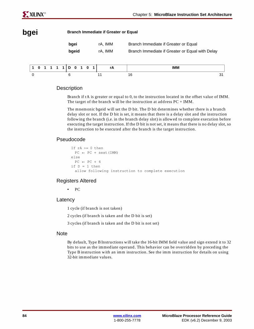
84 www.xilinx.com MicroBlaze Processor Reference Guide1-800-255-7778 EDK (v6.2) December 9, 2003
Chapter 5: MicroBlaze Instruction Set ArchitectureR
bgei Branch Immediate if Greater or Equal
Description
Branch if rA is greater or equal to 0, to the instruction located in the offset value of IMM.The target of the branch will be the instruction at address PC + IMM.
The mnemonic bgeid will set the D bit. The D bit determines whether there is a branchdelay slot or not. If the D bit is set, it means that there is a delay slot and the instructionfollowing the branch (i.e. in the branch delay slot) is allowed to complete execution beforeexecuting the target instruction. If the D bit is not set, it means that there is no delay slot, sothe instruction to be executed after the branch is the target instruction.
Pseudocode
If rA >= 0 thenPC ← PC + sext(IMM)
elsePC ← PC + 4
if D = 1 thenallow following instruction to complete execution
Registers Altered
• PC
Latency
1 cycle (if branch is not taken)
2 cycles (if branch is taken and the D bit is set)
3 cycles (if branch is taken and the D bit is not set)
Note
By default, Type B Instructions will take the 16-bit IMM field value and sign extend it to 32bits to use as the immediate operand. This behavior can be overridden by preceding theType B instruction with an imm instruction. See the imm instruction for details on using32-bit immediate values.
bgei rA, IMM Branch Immediate if Greater or Equal
bgeid rA, IMM Branch Immediate if Greater or Equal with Delay
1 0 1 1 1 1 D 0 1 0 1 rA IMM
0 6 11 16 31
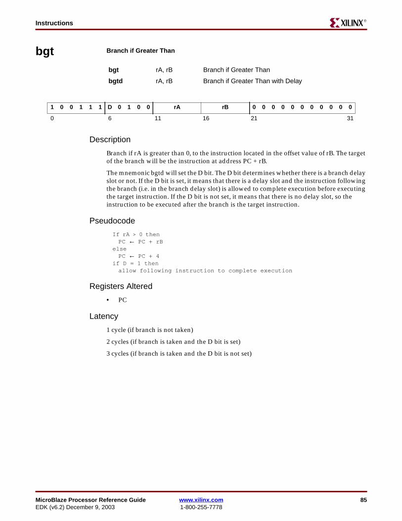
MicroBlaze Processor Reference Guide www.xilinx.com 85EDK (v6.2) December 9, 2003 1-800-255-7778
InstructionsR
bgt Branch if Greater Than
Description
Branch if rA is greater than 0, to the instruction located in the offset value of rB. The targetof the branch will be the instruction at address PC + rB.
The mnemonic bgtd will set the D bit. The D bit determines whether there is a branch delayslot or not. If the D bit is set, it means that there is a delay slot and the instruction followingthe branch (i.e. in the branch delay slot) is allowed to complete execution before executingthe target instruction. If the D bit is not set, it means that there is no delay slot, so theinstruction to be executed after the branch is the target instruction.
Pseudocode
If rA > 0 thenPC ← PC + rB
elsePC ← PC + 4
if D = 1 thenallow following instruction to complete execution
Registers Altered
• PC
Latency
1 cycle (if branch is not taken)
2 cycles (if branch is taken and the D bit is set)
3 cycles (if branch is taken and the D bit is not set)
bgt rA, rB Branch if Greater Than
bgtd rA, rB Branch if Greater Than with Delay
1 0 0 1 1 1 D 0 1 0 0 rA rB 0 0 0 0 0 0 0 0 0 0 0
0 6 11 16 21 31

86 www.xilinx.com MicroBlaze Processor Reference Guide1-800-255-7778 EDK (v6.2) December 9, 2003
Chapter 5: MicroBlaze Instruction Set ArchitectureR
bgti Branch Immediate if Greater Than
Description
Branch if rA is greater than 0, to the instruction located in the offset value of IMM. Thetarget of the branch will be the instruction at address PC + IMM.
The mnemonic bgtid will set the D bit. The D bit determines whether there is a branchdelay slot or not. If the D bit is set, it means that there is a delay slot and the instructionfollowing the branch (i.e. in the branch delay slot) is allowed to complete execution beforeexecuting the target instruction. If the D bit is not set, it means that there is no delay slot, sothe instruction to be executed after the branch is the target instruction.
Pseudocode
If rA > 0 thenPC ← PC + sext(IMM)
elsePC ← PC + 4
if D = 1 thenallow following instruction to complete execution
Registers Altered
• PC
Latency
1 cycle (if branch is not taken)
2 cycles (if branch is taken and the D bit is set)
3 cycles (if branch is taken and the D bit is not set)
Note
By default, Type B Instructions will take the 16-bit IMM field value and sign extend it to 32bits to use as the immediate operand. This behavior can be overridden by preceding theType B instruction with an imm instruction. See the imm instruction for details on using32-bit immediate values.
bgti rA, IMM Branch Immediate if Greater Than
bgtid rA, IMM Branch Immediate if Greater Than with Delay
1 0 1 1 1 1 D 0 1 0 0 rA IMM
0 6 11 16 31
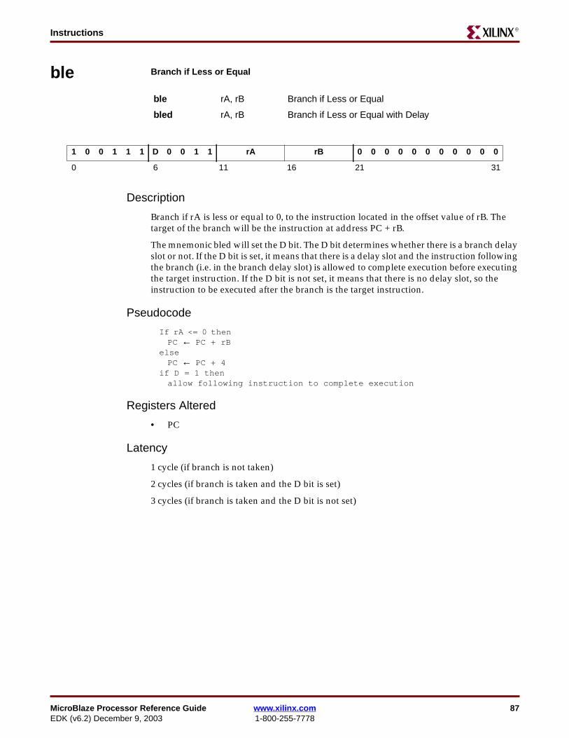
MicroBlaze Processor Reference Guide www.xilinx.com 87EDK (v6.2) December 9, 2003 1-800-255-7778
InstructionsR
ble Branch if Less or Equal
Description
Branch if rA is less or equal to 0, to the instruction located in the offset value of rB. Thetarget of the branch will be the instruction at address PC + rB.
The mnemonic bled will set the D bit. The D bit determines whether there is a branch delayslot or not. If the D bit is set, it means that there is a delay slot and the instruction followingthe branch (i.e. in the branch delay slot) is allowed to complete execution before executingthe target instruction. If the D bit is not set, it means that there is no delay slot, so theinstruction to be executed after the branch is the target instruction.
Pseudocode
If rA <= 0 thenPC ← PC + rB
elsePC ← PC + 4
if D = 1 thenallow following instruction to complete execution
Registers Altered
• PC
Latency
1 cycle (if branch is not taken)
2 cycles (if branch is taken and the D bit is set)
3 cycles (if branch is taken and the D bit is not set)
ble rA, rB Branch if Less or Equal
bled rA, rB Branch if Less or Equal with Delay
1 0 0 1 1 1 D 0 0 1 1 rA rB 0 0 0 0 0 0 0 0 0 0 0
0 6 11 16 21 31
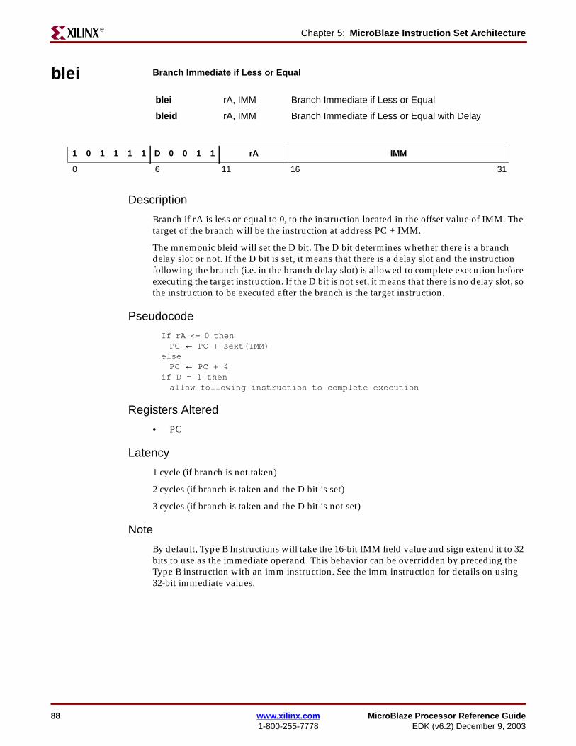
88 www.xilinx.com MicroBlaze Processor Reference Guide1-800-255-7778 EDK (v6.2) December 9, 2003
Chapter 5: MicroBlaze Instruction Set ArchitectureR
blei Branch Immediate if Less or Equal
Description
Branch if rA is less or equal to 0, to the instruction located in the offset value of IMM. Thetarget of the branch will be the instruction at address PC + IMM.
The mnemonic bleid will set the D bit. The D bit determines whether there is a branchdelay slot or not. If the D bit is set, it means that there is a delay slot and the instructionfollowing the branch (i.e. in the branch delay slot) is allowed to complete execution beforeexecuting the target instruction. If the D bit is not set, it means that there is no delay slot, sothe instruction to be executed after the branch is the target instruction.
Pseudocode
If rA <= 0 thenPC ← PC + sext(IMM)
elsePC ← PC + 4
if D = 1 thenallow following instruction to complete execution
Registers Altered
• PC
Latency
1 cycle (if branch is not taken)
2 cycles (if branch is taken and the D bit is set)
3 cycles (if branch is taken and the D bit is not set)
Note
By default, Type B Instructions will take the 16-bit IMM field value and sign extend it to 32bits to use as the immediate operand. This behavior can be overridden by preceding theType B instruction with an imm instruction. See the imm instruction for details on using32-bit immediate values.
blei rA, IMM Branch Immediate if Less or Equal
bleid rA, IMM Branch Immediate if Less or Equal with Delay
1 0 1 1 1 1 D 0 0 1 1 rA IMM
0 6 11 16 31

MicroBlaze Processor Reference Guide www.xilinx.com 89EDK (v6.2) December 9, 2003 1-800-255-7778
InstructionsR
blt Branch if Less Than
Description
Branch if rA is less than 0, to the instruction located in the offset value of rB. The target ofthe branch will be the instruction at address PC + rB.
The mnemonic bltd will set the D bit. The D bit determines whether there is a branch delayslot or not. If the D bit is set, it means that there is a delay slot and the instruction followingthe branch (i.e. in the branch delay slot) is allowed to complete execution before executingthe target instruction. If the D bit is not set, it means that there is no delay slot, so theinstruction to be executed after the branch is the target instruction.
Pseudocode
If rA < 0 thenPC ← PC + rB
elsePC ← PC + 4
if D = 1 thenallow following instruction to complete execution
Registers Altered
• PC
Latency
1 cycle (if branch is not taken)
2 cycles (if branch is taken and the D bit is set)
3 cycles (if branch is taken and the D bit is not set)
blt rA, rB Branch if Less Than
bltd rA, rB Branch if Less Than with Delay
1 0 0 1 1 1 D 0 0 1 0 rA rB 0 0 0 0 0 0 0 0 0 0 0
0 6 11 16 21 31
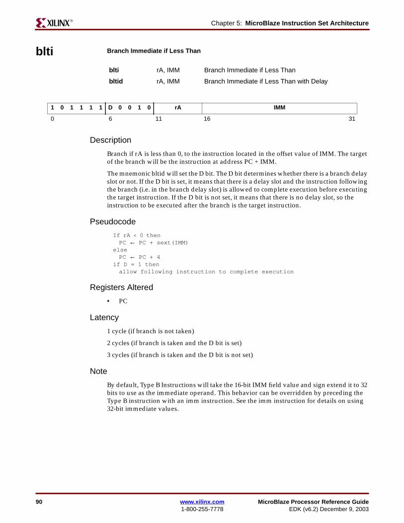
90 www.xilinx.com MicroBlaze Processor Reference Guide1-800-255-7778 EDK (v6.2) December 9, 2003
Chapter 5: MicroBlaze Instruction Set ArchitectureR
blti Branch Immediate if Less Than
Description
Branch if rA is less than 0, to the instruction located in the offset value of IMM. The targetof the branch will be the instruction at address PC + IMM.
The mnemonic bltid will set the D bit. The D bit determines whether there is a branch delayslot or not. If the D bit is set, it means that there is a delay slot and the instruction followingthe branch (i.e. in the branch delay slot) is allowed to complete execution before executingthe target instruction. If the D bit is not set, it means that there is no delay slot, so theinstruction to be executed after the branch is the target instruction.
Pseudocode
If rA < 0 thenPC ← PC + sext(IMM)
elsePC ← PC + 4
if D = 1 thenallow following instruction to complete execution
Registers Altered
• PC
Latency
1 cycle (if branch is not taken)
2 cycles (if branch is taken and the D bit is set)
3 cycles (if branch is taken and the D bit is not set)
Note
By default, Type B Instructions will take the 16-bit IMM field value and sign extend it to 32bits to use as the immediate operand. This behavior can be overridden by preceding theType B instruction with an imm instruction. See the imm instruction for details on using32-bit immediate values.
blti rA, IMM Branch Immediate if Less Than
bltid rA, IMM Branch Immediate if Less Than with Delay
1 0 1 1 1 1 D 0 0 1 0 rA IMM
0 6 11 16 31

MicroBlaze Processor Reference Guide www.xilinx.com 91EDK (v6.2) December 9, 2003 1-800-255-7778
InstructionsR
bne Branch if Not Equal
Description
Branch if rA not equal to 0, to the instruction located in the offset value of rB. The target ofthe branch will be the instruction at address PC + rB.
The mnemonic bned will set the D bit. The D bit determines whether there is a branchdelay slot or not. If the D bit is set, it means that there is a delay slot and the instructionfollowing the branch (i.e. in the branch delay slot) is allowed to complete execution beforeexecuting the target instruction. If the D bit is not set, it means that there is no delay slot, sothe instruction to be executed after the branch is the target instruction.
Pseudocode
If rA ≠ 0 thenPC ← PC + rB
elsePC ← PC + 4
if D = 1 thenallow following instruction to complete execution
Registers Altered
• PC
Latency
1 cycle (if branch is not taken)
2 cycles (if branch is taken and the D bit is set)
3 cycles (if branch is taken and the D bit is not set)
bne rA, rB Branch if Not Equal
bned rA, rB Branch if Not Equal with Delay
1 0 0 1 1 1 D 0 0 0 1 rA rB 0 0 0 0 0 0 0 0 0 0 0
0 6 11 16 21 31
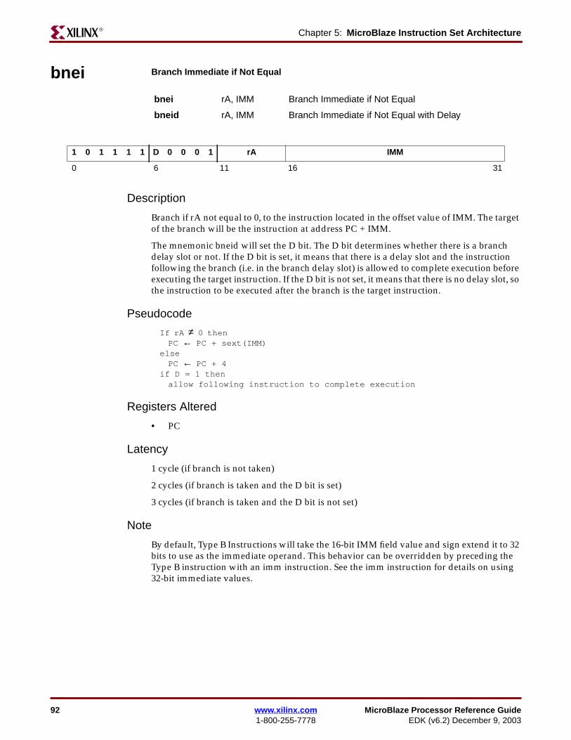
92 www.xilinx.com MicroBlaze Processor Reference Guide1-800-255-7778 EDK (v6.2) December 9, 2003
Chapter 5: MicroBlaze Instruction Set ArchitectureR
bnei Branch Immediate if Not Equal
Description
Branch if rA not equal to 0, to the instruction located in the offset value of IMM. The targetof the branch will be the instruction at address PC + IMM.
The mnemonic bneid will set the D bit. The D bit determines whether there is a branchdelay slot or not. If the D bit is set, it means that there is a delay slot and the instructionfollowing the branch (i.e. in the branch delay slot) is allowed to complete execution beforeexecuting the target instruction. If the D bit is not set, it means that there is no delay slot, sothe instruction to be executed after the branch is the target instruction.
Pseudocode
If rA ≠ 0 thenPC ← PC + sext(IMM)
elsePC ← PC + 4
if D = 1 thenallow following instruction to complete execution
Registers Altered
• PC
Latency
1 cycle (if branch is not taken)
2 cycles (if branch is taken and the D bit is set)
3 cycles (if branch is taken and the D bit is not set)
Note
By default, Type B Instructions will take the 16-bit IMM field value and sign extend it to 32bits to use as the immediate operand. This behavior can be overridden by preceding theType B instruction with an imm instruction. See the imm instruction for details on using32-bit immediate values.
bnei rA, IMM Branch Immediate if Not Equal
bneid rA, IMM Branch Immediate if Not Equal with Delay
1 0 1 1 1 1 D 0 0 0 1 rA IMM
0 6 11 16 31
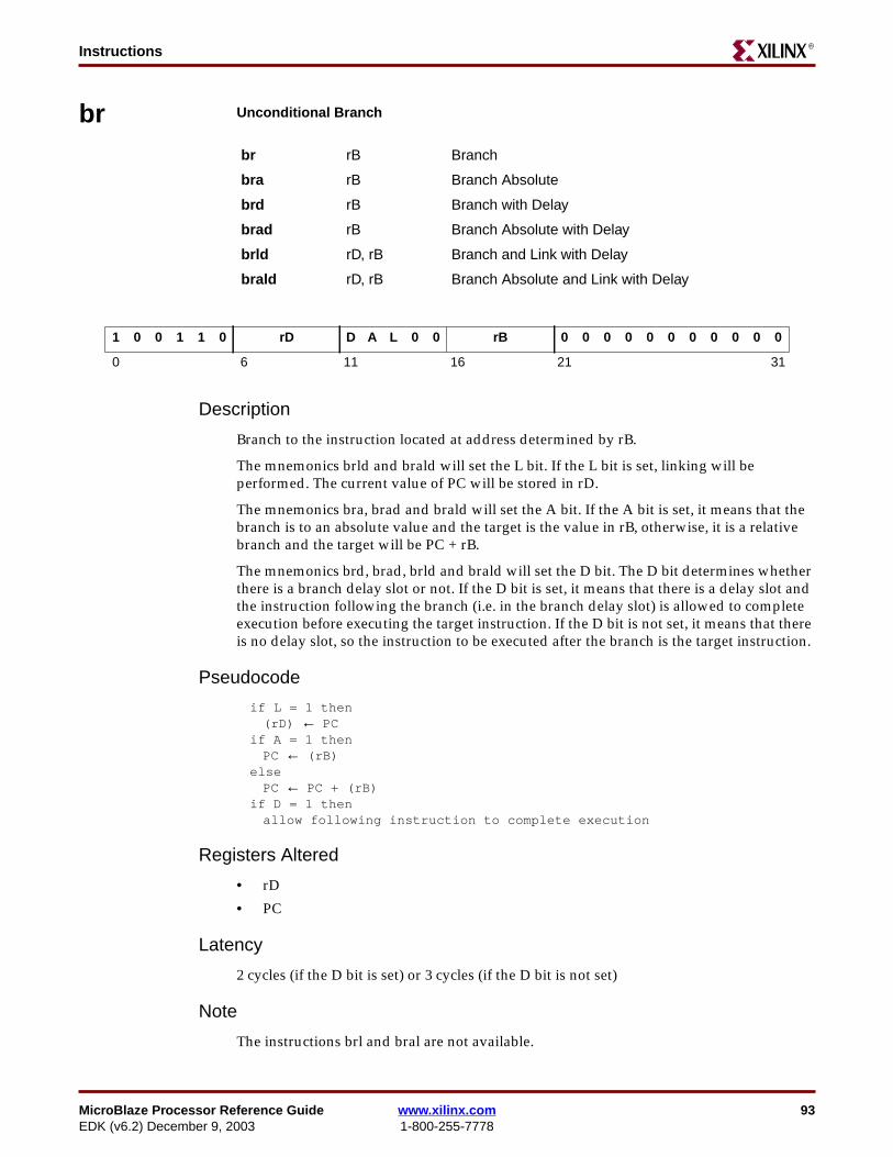
MicroBlaze Processor Reference Guide www.xilinx.com 93EDK (v6.2) December 9, 2003 1-800-255-7778
InstructionsR
br Unconditional Branch
Description
Branch to the instruction located at address determined by rB.
The mnemonics brld and brald will set the L bit. If the L bit is set, linking will beperformed. The current value of PC will be stored in rD.
The mnemonics bra, brad and brald will set the A bit. If the A bit is set, it means that thebranch is to an absolute value and the target is the value in rB, otherwise, it is a relativebranch and the target will be PC + rB.
The mnemonics brd, brad, brld and brald will set the D bit. The D bit determines whetherthere is a branch delay slot or not. If the D bit is set, it means that there is a delay slot andthe instruction following the branch (i.e. in the branch delay slot) is allowed to completeexecution before executing the target instruction. If the D bit is not set, it means that thereis no delay slot, so the instruction to be executed after the branch is the target instruction.
Pseudocode
if L = 1 then(rD) ← PC
if A = 1 thenPC ← (rB)
elsePC ← PC + (rB)
if D = 1 thenallow following instruction to complete execution
Registers Altered
• rD
• PC
Latency
2 cycles (if the D bit is set) or 3 cycles (if the D bit is not set)
Note
The instructions brl and bral are not available.
br rB Branch
bra rB Branch Absolute
brd rB Branch with Delay
brad rB Branch Absolute with Delay
brld rD, rB Branch and Link with Delay
brald rD, rB Branch Absolute and Link with Delay
1 0 0 1 1 0 rD D A L 0 0 rB 0 0 0 0 0 0 0 0 0 0 0
0 6 11 16 21 31
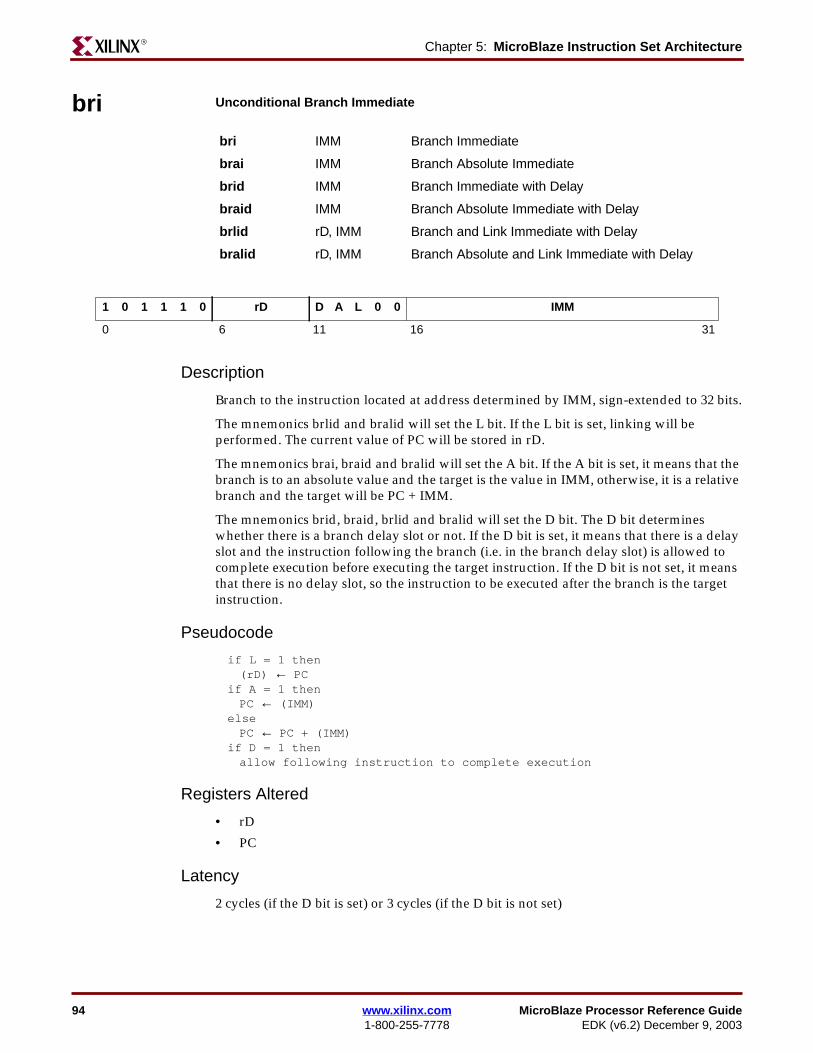
94 www.xilinx.com MicroBlaze Processor Reference Guide1-800-255-7778 EDK (v6.2) December 9, 2003
Chapter 5: MicroBlaze Instruction Set ArchitectureR
bri Unconditional Branch Immediate
Description
Branch to the instruction located at address determined by IMM, sign-extended to 32 bits.
The mnemonics brlid and bralid will set the L bit. If the L bit is set, linking will beperformed. The current value of PC will be stored in rD.
The mnemonics brai, braid and bralid will set the A bit. If the A bit is set, it means that thebranch is to an absolute value and the target is the value in IMM, otherwise, it is a relativebranch and the target will be PC + IMM.
The mnemonics brid, braid, brlid and bralid will set the D bit. The D bit determineswhether there is a branch delay slot or not. If the D bit is set, it means that there is a delayslot and the instruction following the branch (i.e. in the branch delay slot) is allowed tocomplete execution before executing the target instruction. If the D bit is not set, it meansthat there is no delay slot, so the instruction to be executed after the branch is the targetinstruction.
Pseudocode
if L = 1 then(rD) ← PC
if A = 1 thenPC ← (IMM)
elsePC ← PC + (IMM)
if D = 1 thenallow following instruction to complete execution
Registers Altered
• rD
• PC
Latency
2 cycles (if the D bit is set) or 3 cycles (if the D bit is not set)
bri IMM Branch Immediate
brai IMM Branch Absolute Immediate
brid IMM Branch Immediate with Delay
braid IMM Branch Absolute Immediate with Delay
brlid rD, IMM Branch and Link Immediate with Delay
bralid rD, IMM Branch Absolute and Link Immediate with Delay
1 0 1 1 1 0 rD D A L 0 0 IMM
0 6 11 16 31
MicroBlaze Processor Reference Guide www.xilinx.com 95EDK (v6.2) December 9, 2003 1-800-255-7778
InstructionsR
Notes
The instructions brli and brali are not available.
By default, Type B Instructions will take the 16-bit IMM field value and sign extend it to 32bits to use as the immediate operand. This behavior can be overridden by preceding theType B instruction with an imm instruction. See the imm instruction for details on using32-bit immediate values.
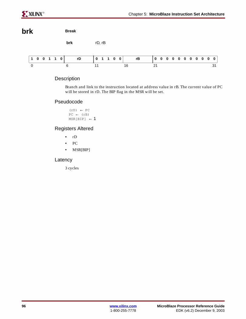
96 www.xilinx.com MicroBlaze Processor Reference Guide1-800-255-7778 EDK (v6.2) December 9, 2003
Chapter 5: MicroBlaze Instruction Set ArchitectureR
brk Break
Description
Branch and link to the instruction located at address value in rB. The current value of PCwill be stored in rD. The BIP flag in the MSR will be set.
Pseudocode
(rD) ← PCPC ← (rB)MSR[BIP] ← 1
Registers Altered
• rD
• PC
• MSR[BIP]
Latency
3 cycles
brk rD, rB
1 0 0 1 1 0 rD 0 1 1 0 0 rB 0 0 0 0 0 0 0 0 0 0 0
0 6 11 16 21 31
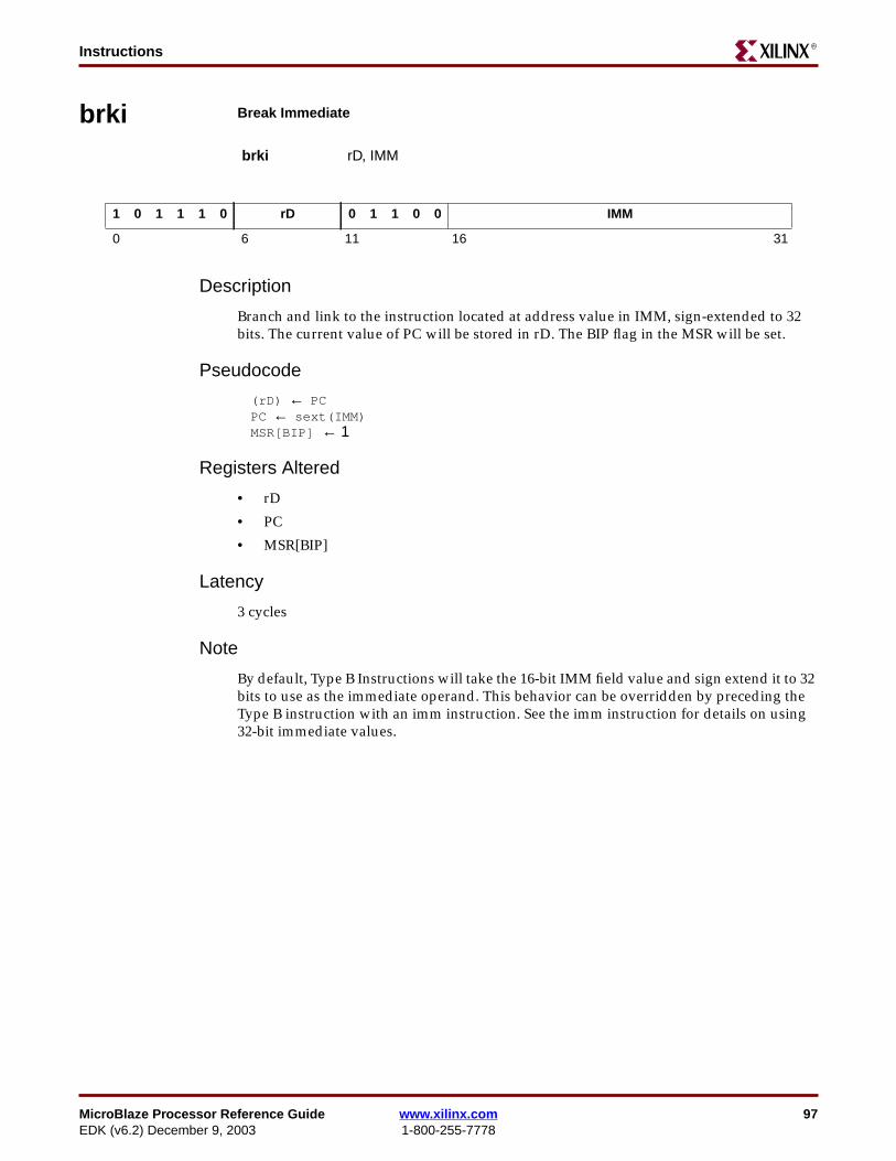
MicroBlaze Processor Reference Guide www.xilinx.com 97EDK (v6.2) December 9, 2003 1-800-255-7778
InstructionsR
brki Break Immediate
Description
Branch and link to the instruction located at address value in IMM, sign-extended to 32bits. The current value of PC will be stored in rD. The BIP flag in the MSR will be set.
Pseudocode
(rD) ← PCPC ← sext(IMM)MSR[BIP] ← 1
Registers Altered
• rD
• PC
• MSR[BIP]
Latency
3 cycles
Note
By default, Type B Instructions will take the 16-bit IMM field value and sign extend it to 32bits to use as the immediate operand. This behavior can be overridden by preceding theType B instruction with an imm instruction. See the imm instruction for details on using32-bit immediate values.
brki rD, IMM
1 0 1 1 1 0 rD 0 1 1 0 0 IMM
0 6 11 16 31
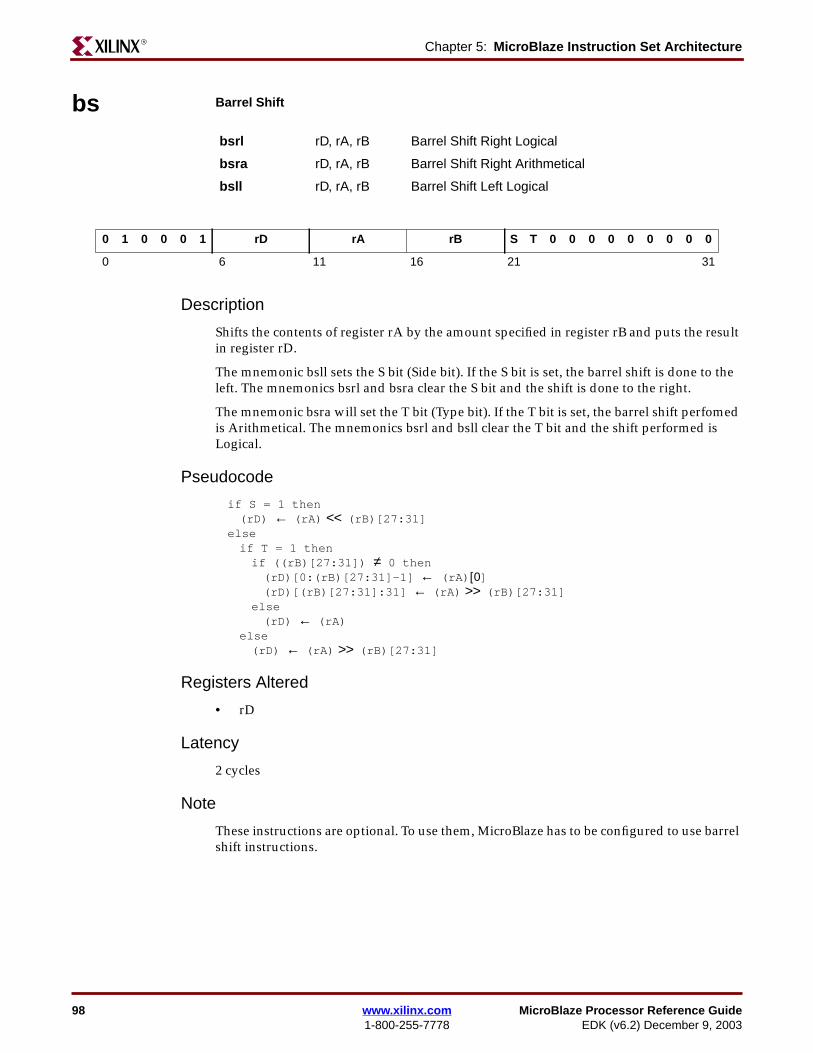
98 www.xilinx.com MicroBlaze Processor Reference Guide1-800-255-7778 EDK (v6.2) December 9, 2003
Chapter 5: MicroBlaze Instruction Set ArchitectureR
bs Barrel Shift
Description
Shifts the contents of register rA by the amount specified in register rB and puts the resultin register rD.
The mnemonic bsll sets the S bit (Side bit). If the S bit is set, the barrel shift is done to theleft. The mnemonics bsrl and bsra clear the S bit and the shift is done to the right.
The mnemonic bsra will set the T bit (Type bit). If the T bit is set, the barrel shift perfomedis Arithmetical. The mnemonics bsrl and bsll clear the T bit and the shift performed isLogical.
Pseudocode
if S = 1 then(rD) ← (rA) << (rB)[27:31]
elseif T = 1 thenif ((rB)[27:31]) ≠ 0 then(rD)[0:(rB)[27:31]-1] ← (rA)[0](rD)[(rB)[27:31]:31] ← (rA) >> (rB)[27:31]
else(rD) ← (rA)
else(rD) ← (rA) >> (rB)[27:31]
Registers Altered
• rD
Latency
2 cycles
Note
These instructions are optional. To use them, MicroBlaze has to be configured to use barrelshift instructions.
bsrl rD, rA, rB Barrel Shift Right Logical
bsra rD, rA, rB Barrel Shift Right Arithmetical
bsll rD, rA, rB Barrel Shift Left Logical
0 1 0 0 0 1 rD rA rB S T 0 0 0 0 0 0 0 0 0
0 6 11 16 21 31
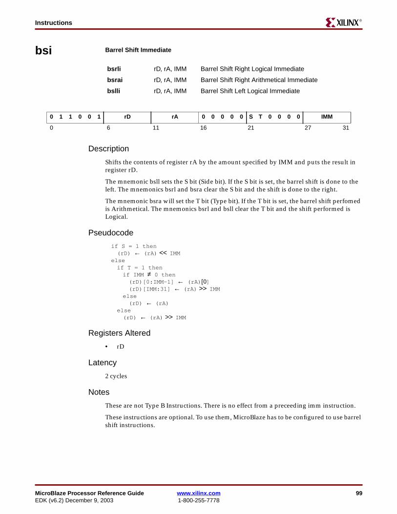
MicroBlaze Processor Reference Guide www.xilinx.com 99EDK (v6.2) December 9, 2003 1-800-255-7778
InstructionsR
bsi Barrel Shift Immediate
Description
Shifts the contents of register rA by the amount specified by IMM and puts the result inregister rD.
The mnemonic bsll sets the S bit (Side bit). If the S bit is set, the barrel shift is done to theleft. The mnemonics bsrl and bsra clear the S bit and the shift is done to the right.
The mnemonic bsra will set the T bit (Type bit). If the T bit is set, the barrel shift perfomedis Arithmetical. The mnemonics bsrl and bsll clear the T bit and the shift performed isLogical.
Pseudocode
if S = 1 then(rD) ← (rA) << IMM
elseif T = 1 thenif IMM ≠ 0 then(rD)[0:IMM-1] ← (rA)[0](rD)[IMM:31] ← (rA) >> IMM
else(rD) ← (rA)
else(rD) ← (rA) >> IMM
Registers Altered
• rD
Latency
2 cycles
Notes
These are not Type B Instructions. There is no effect from a preceeding imm instruction.
These instructions are optional. To use them, MicroBlaze has to be configured to use barrelshift instructions.
bsrli rD, rA, IMM Barrel Shift Right Logical Immediate
bsrai rD, rA, IMM Barrel Shift Right Arithmetical Immediate
bslli rD, rA, IMM Barrel Shift Left Logical Immediate
0 1 1 0 0 1 rD rA 0 0 0 0 0 S T 0 0 0 0 IMM
0 6 11 16 21 27 31
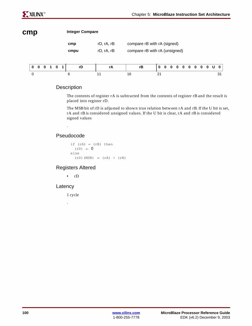
100 www.xilinx.com MicroBlaze Processor Reference Guide1-800-255-7778 EDK (v6.2) December 9, 2003
Chapter 5: MicroBlaze Instruction Set ArchitectureR
cmp Integer Compare
Description
The contents of register rA is subtracted from the contents of register rB and the result isplaced into register rD.
The MSB bit of rD is adjusted to shown true relation between rA and rB. If the U bit is set,rA and rB is considered unsigned values. If the U bit is clear, rA and rB is consideredsigned values
.
Pseudocode
if (rA) = (rB) then(rD) ← 0
else(rD)(MSB) ← (rA) > (rB)
Registers Altered
• rD
Latency
1 cycle
.
cmp rD, rA, rB compare rB with rA (signed)
cmpu rD, rA, rB compare rB with rA (unsigned)
0 0 0 1 0 1 rD rA rB 0 0 0 0 0 0 0 0 0 U 0
0 6 11 16 21 31
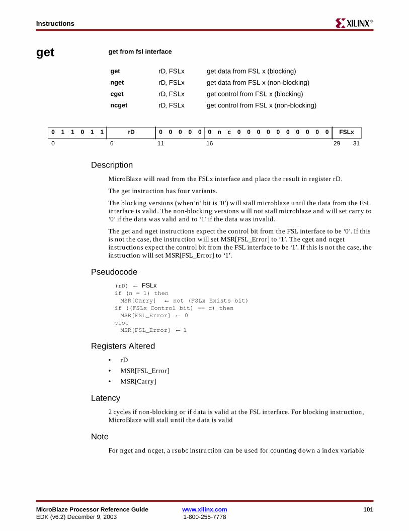
MicroBlaze Processor Reference Guide www.xilinx.com 101EDK (v6.2) December 9, 2003 1-800-255-7778
InstructionsR
get get from fsl interface
Description
MicroBlaze will read from the FSLx interface and place the result in register rD.
The get instruction has four variants.
The blocking versions (when‘n’ bit is ‘0’) will stall microblaze until the data from the FSLinterface is valid. The non-blocking versions will not stall microblaze and will set carry to‘0’ if the data was valid and to ‘1’ if the data was invalid.
The get and nget instructions expect the control bit from the FSL interface to be ‘0’. If thisis not the case, the instruction will set MSR[FSL_Error] to ‘1’. The cget and ncgetinstructions expect the control bit from the FSL interface to be ‘1’. If this is not the case, theinstruction will set MSR[FSL_Error] to ‘1’.
Pseudocode
(rD) ← FSLxif (n = 1) thenMSR[Carry] ← not (FSLx Exists bit)
if ((FSLx Control bit) == c) thenMSR[FSL_Error] ← 0
elseMSR[FSL_Error] ← 1
Registers Altered
• rD
• MSR[FSL_Error]
• MSR[Carry]
Latency
2 cycles if non-blocking or if data is valid at the FSL interface. For blocking instruction,MicroBlaze will stall until the data is valid
Note
For nget and ncget, a rsubc instruction can be used for counting down a index variable
get rD, FSLx get data from FSL x (blocking)
nget rD, FSLx get data from FSL x (non-blocking)
cget rD, FSLx get control from FSL x (blocking)
ncget rD, FSLx get control from FSL x (non-blocking)
0 1 1 0 1 1 rD 0 0 0 0 0 0 n c 0 0 0 0 0 0 0 0 0 0 FSLx
0 6 11 16 29 31
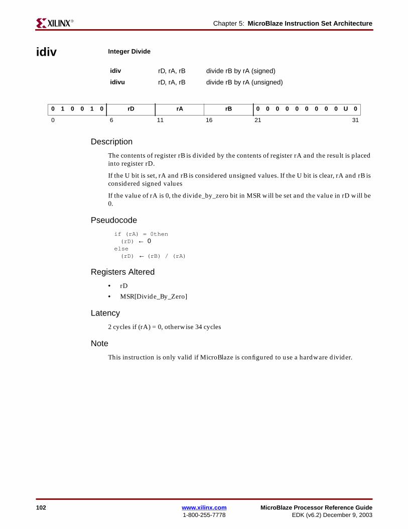
102 www.xilinx.com MicroBlaze Processor Reference Guide1-800-255-7778 EDK (v6.2) December 9, 2003
Chapter 5: MicroBlaze Instruction Set ArchitectureR
idiv Integer Divide
Description
The contents of register rB is divided by the contents of register rA and the result is placedinto register rD.
If the U bit is set, rA and rB is considered unsigned values. If the U bit is clear, rA and rB isconsidered signed values
If the value of rA is 0, the divide_by_zero bit in MSR will be set and the value in rD will be0.
Pseudocode
if (rA) = 0then(rD) ← 0
else(rD) ← (rB) / (rA)
Registers Altered
• rD
• MSR[Divide_By_Zero]
Latency
2 cycles if (rA) = 0, otherwise 34 cycles
Note
This instruction is only valid if MicroBlaze is configured to use a hardware divider.
idiv rD, rA, rB divide rB by rA (signed)
idivu rD, rA, rB divide rB by rA (unsigned)
0 1 0 0 1 0 rD rA rB 0 0 0 0 0 0 0 0 0 U 0
0 6 11 16 21 31
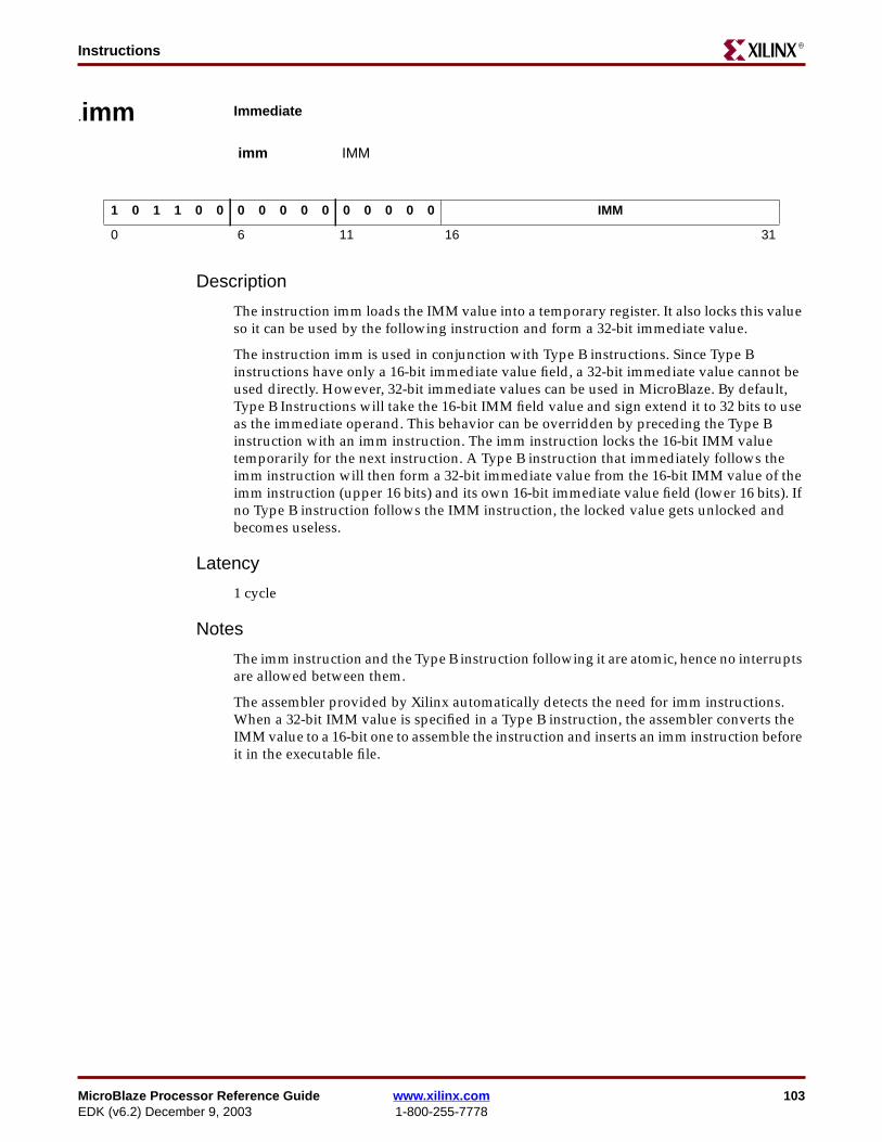
MicroBlaze Processor Reference Guide www.xilinx.com 103EDK (v6.2) December 9, 2003 1-800-255-7778
InstructionsR
.imm Immediate
Description
The instruction imm loads the IMM value into a temporary register. It also locks this valueso it can be used by the following instruction and form a 32-bit immediate value.
The instruction imm is used in conjunction with Type B instructions. Since Type Binstructions have only a 16-bit immediate value field, a 32-bit immediate value cannot beused directly. However, 32-bit immediate values can be used in MicroBlaze. By default,Type B Instructions will take the 16-bit IMM field value and sign extend it to 32 bits to useas the immediate operand. This behavior can be overridden by preceding the Type Binstruction with an imm instruction. The imm instruction locks the 16-bit IMM valuetemporarily for the next instruction. A Type B instruction that immediately follows theimm instruction will then form a 32-bit immediate value from the 16-bit IMM value of theimm instruction (upper 16 bits) and its own 16-bit immediate value field (lower 16 bits). Ifno Type B instruction follows the IMM instruction, the locked value gets unlocked andbecomes useless.
Latency
1 cycle
Notes
The imm instruction and the Type B instruction following it are atomic, hence no interruptsare allowed between them.
The assembler provided by Xilinx automatically detects the need for imm instructions.When a 32-bit IMM value is specified in a Type B instruction, the assembler converts theIMM value to a 16-bit one to assemble the instruction and inserts an imm instruction beforeit in the executable file.
imm IMM
1 0 1 1 0 0 0 0 0 0 0 0 0 0 0 0 IMM
0 6 11 16 31
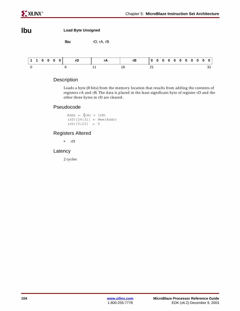
104 www.xilinx.com MicroBlaze Processor Reference Guide1-800-255-7778 EDK (v6.2) December 9, 2003
Chapter 5: MicroBlaze Instruction Set ArchitectureR
lbu Load Byte Unsigned
Description
Loads a byte (8 bits) from the memory location that results from adding the contents ofregisters rA and rB. The data is placed in the least significant byte of register rD and theother three bytes in rD are cleared.
Pseudocode
Addr ← (rA) + (rB)(rD)[24:31] ← Mem(Addr)(rD)[0:23] ← 0
Registers Altered
• rD
Latency
2 cycles
lbu rD, rA, rB
1 1 0 0 0 0 rD rA rB 0 0 0 0 0 0 0 0 0 0 0
0 6 11 16 21 31
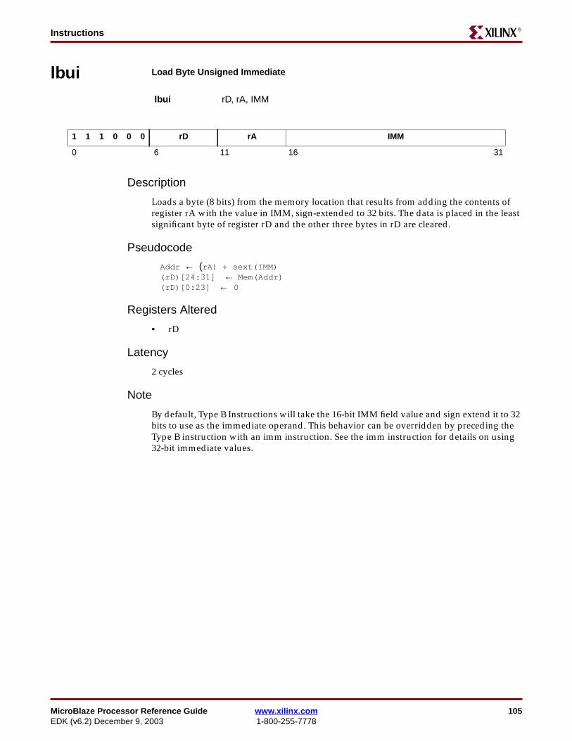
MicroBlaze Processor Reference Guide www.xilinx.com 105EDK (v6.2) December 9, 2003 1-800-255-7778
InstructionsR
lbui Load Byte Unsigned Immediate
Description
Loads a byte (8 bits) from the memory location that results from adding the contents ofregister rA with the value in IMM, sign-extended to 32 bits. The data is placed in the leastsignificant byte of register rD and the other three bytes in rD are cleared.
Pseudocode
Addr ← (rA) + sext(IMM)(rD)[24:31] ← Mem(Addr)(rD)[0:23] ← 0
Registers Altered
• rD
Latency
2 cycles
Note
By default, Type B Instructions will take the 16-bit IMM field value and sign extend it to 32bits to use as the immediate operand. This behavior can be overridden by preceding theType B instruction with an imm instruction. See the imm instruction for details on using32-bit immediate values.
lbui rD, rA, IMM
1 1 1 0 0 0 rD rA IMM
0 6 11 16 31

106 www.xilinx.com MicroBlaze Processor Reference Guide1-800-255-7778 EDK (v6.2) December 9, 2003
Chapter 5: MicroBlaze Instruction Set ArchitectureR
lhu Load Halfword Unsigned
Description
Loads a halfword (16 bits) from the halfword aligned memory location that results fromadding the contents of registers rA and rB. The data is placed in the least significanthalfword of register rD and the most significant halfword in rD is cleared.
Pseudocode
Addr ← (rA) + (rB)Addr[31] ← 0(rD)[16:31] ← Mem(Addr)(rD)[0:15] ← 0
Registers Altered
• rD
Latency
2 cycles
lhu rD, rA, rB
1 1 0 0 0 1 rD rA rB 0 0 0 0 0 0 0 0 0 0 0
0 6 11 16 21 31
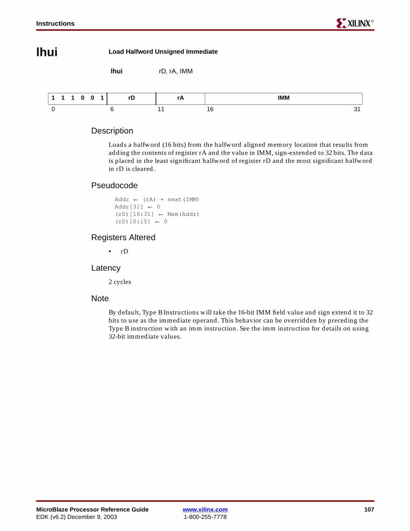
MicroBlaze Processor Reference Guide www.xilinx.com 107EDK (v6.2) December 9, 2003 1-800-255-7778
InstructionsR
lhui Load Halfword Unsigned Immediate
Description
Loads a halfword (16 bits) from the halfword aligned memory location that results fromadding the contents of register rA and the value in IMM, sign-extended to 32 bits. The datais placed in the least significant halfword of register rD and the most significant halfwordin rD is cleared.
Pseudocode
Addr ← (rA) + sext(IMM)Addr[31] ← 0(rD)[16:31] ← Mem(Addr)(rD)[0:15] ← 0
Registers Altered
• rD
Latency
2 cycles
Note
By default, Type B Instructions will take the 16-bit IMM field value and sign extend it to 32bits to use as the immediate operand. This behavior can be overridden by preceding theType B instruction with an imm instruction. See the imm instruction for details on using32-bit immediate values.
lhui rD, rA, IMM
1 1 1 0 0 1 rD rA IMM
0 6 11 16 31

108 www.xilinx.com MicroBlaze Processor Reference Guide1-800-255-7778 EDK (v6.2) December 9, 2003
Chapter 5: MicroBlaze Instruction Set ArchitectureR
lw Load Word
Description
Loads a word (32 bits) from the word aligned memory location that results from addingthe contents of registers rA and rB. The data is placed in register rD.
Pseudocode
Addr ← (rA) + (rB)Addr[30:31] ← 00(rD) ← Mem(Addr)
Registers Altered
• rD
Latency
2 cycles
lw rD, rA, rB
1 1 0 0 1 0 rD rA rB 0 0 0 0 0 0 0 0 0 0 0
0 6 11 16 21 31

MicroBlaze Processor Reference Guide www.xilinx.com 109EDK (v6.2) December 9, 2003 1-800-255-7778
InstructionsR
lwi Load Word Immediate
Description
Loads a word (32 bits) from the word aligned memory location that results from addingthe contents of register rA and the value IMM, sign-extended to 32 bits. The data is placedin register rD.
Pseudocode
Addr ← (rA) + sext(IMM)Addr[30:31] ← 00(rD) ← Mem(Addr)
Registers Altered
• rD
Latency
2 cycles
Note
By default, Type B Instructions will take the 16-bit IMM field value and sign extend it to 32bits to use as the immediate operand. This behavior can be overridden by preceding theType B instruction with an imm instruction. See the imm instruction for details on using32-bit immediate values.
lwi rD, rA, IMM
1 1 1 0 1 0 rD rA IMM
0 6 11 16 31
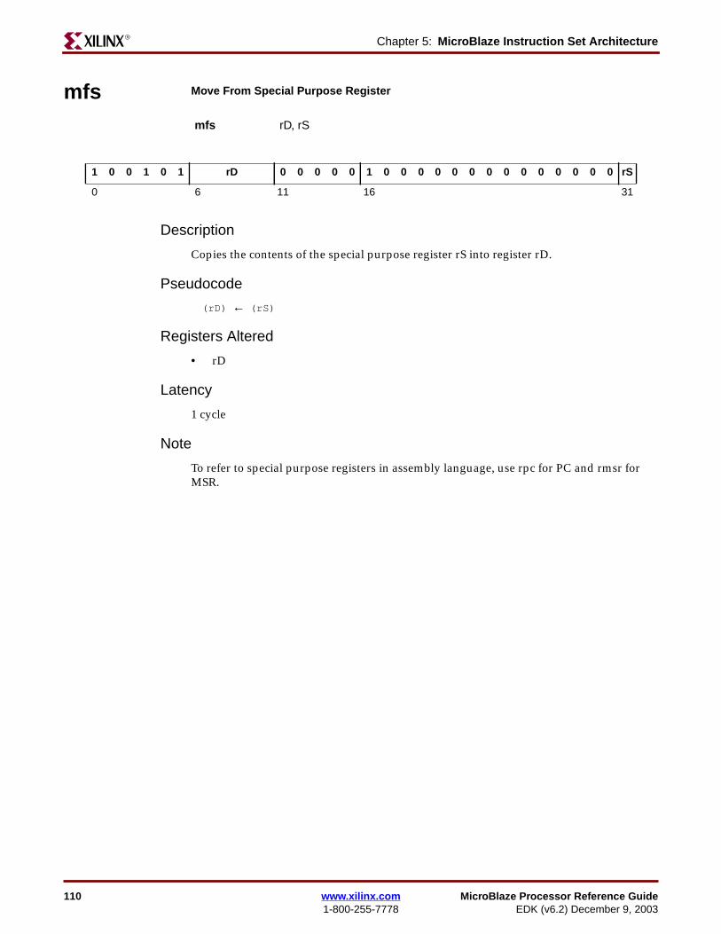
110 www.xilinx.com MicroBlaze Processor Reference Guide1-800-255-7778 EDK (v6.2) December 9, 2003
Chapter 5: MicroBlaze Instruction Set ArchitectureR
mfs Move From Special Purpose Register
Description
Copies the contents of the special purpose register rS into register rD.
Pseudocode
(rD) ← (rS)
Registers Altered
• rD
Latency
1 cycle
Note
To refer to special purpose registers in assembly language, use rpc for PC and rmsr forMSR.
mfs rD, rS
1 0 0 1 0 1 rD 0 0 0 0 0 1 0 0 0 0 0 0 0 0 0 0 0 0 0 0 rS
0 6 11 16 31
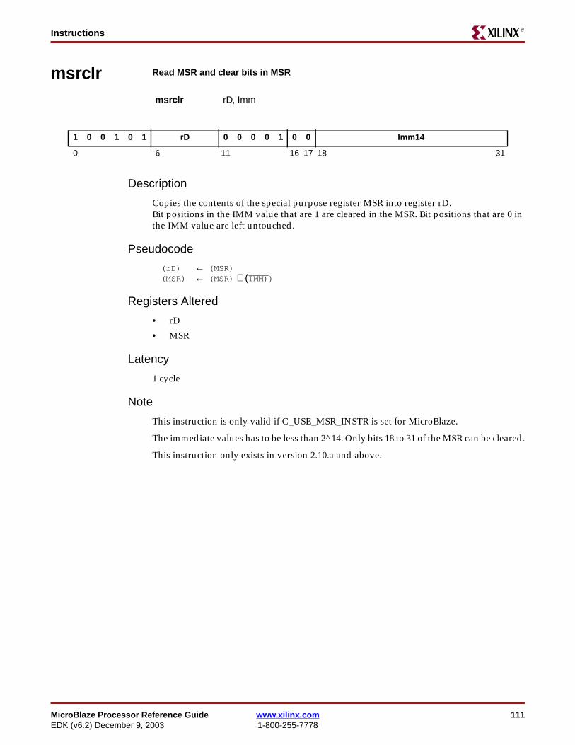
MicroBlaze Processor Reference Guide www.xilinx.com 111EDK (v6.2) December 9, 2003 1-800-255-7778
InstructionsR
msrclr Read MSR and clear bits in MSR
Description
Copies the contents of the special purpose register MSR into register rD.Bit positions in the IMM value that are 1 are cleared in the MSR. Bit positions that are 0 inthe IMM value are left untouched.
Pseudocode
(rD) ← (MSR)(MSR) ← (MSR) ∧ ( IMM))
Registers Altered
• rD
• MSR
Latency
1 cycle
Note
This instruction is only valid if C_USE_MSR_INSTR is set for MicroBlaze.
The immediate values has to be less than 2^14. Only bits 18 to 31 of the MSR can be cleared.
This instruction only exists in version 2.10.a and above.
msrclr rD, Imm
1 0 0 1 0 1 rD 0 0 0 0 1 0 0 Imm14
0 6 11 16 17 18 31
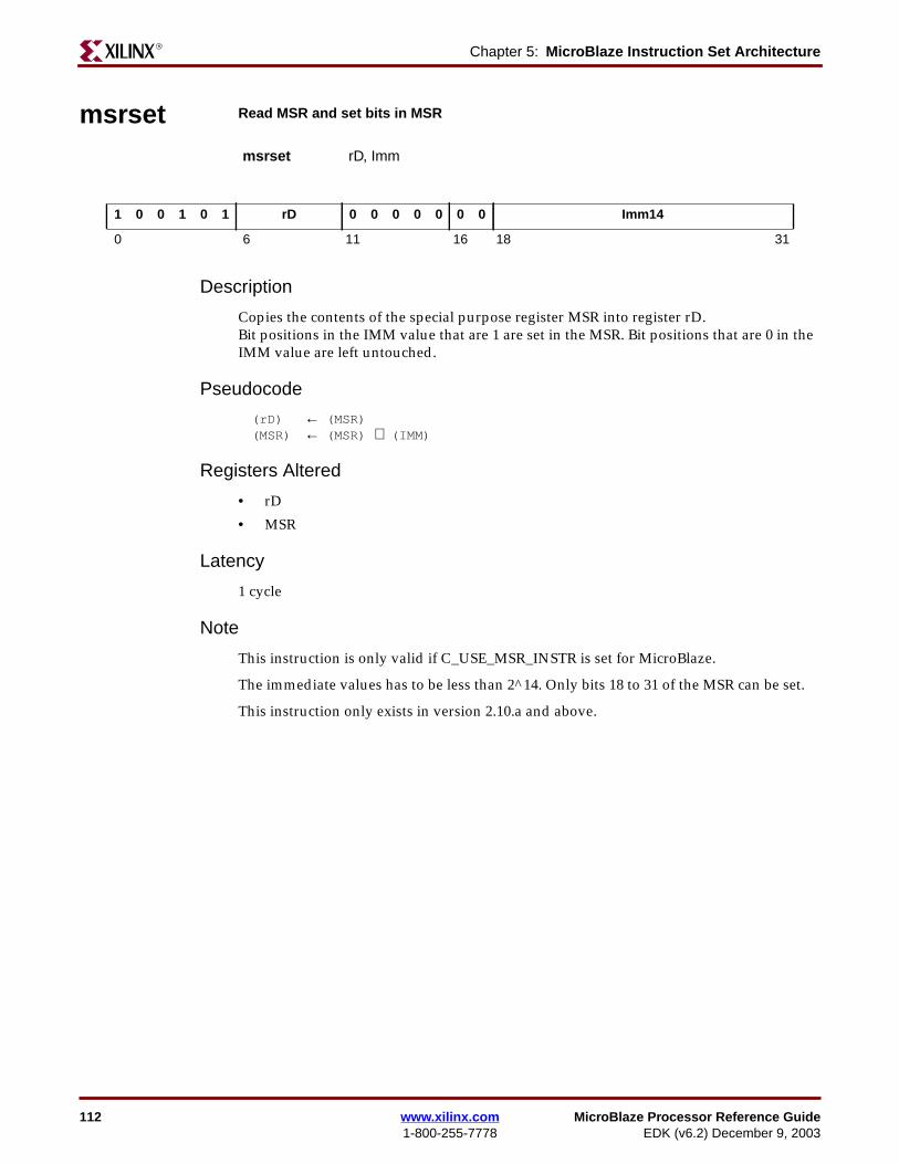
112 www.xilinx.com MicroBlaze Processor Reference Guide1-800-255-7778 EDK (v6.2) December 9, 2003
Chapter 5: MicroBlaze Instruction Set ArchitectureR
msrset Read MSR and set bits in MSR
Description
Copies the contents of the special purpose register MSR into register rD.Bit positions in the IMM value that are 1 are set in the MSR. Bit positions that are 0 in theIMM value are left untouched.
Pseudocode
(rD) ← (MSR)(MSR) ← (MSR) ∨ (IMM)
Registers Altered
• rD
• MSR
Latency
1 cycle
Note
This instruction is only valid if C_USE_MSR_INSTR is set for MicroBlaze.
The immediate values has to be less than 2^14. Only bits 18 to 31 of the MSR can be set.
This instruction only exists in version 2.10.a and above.
msrset rD, Imm
1 0 0 1 0 1 rD 0 0 0 0 0 0 0 Imm14
0 6 11 16 18 31
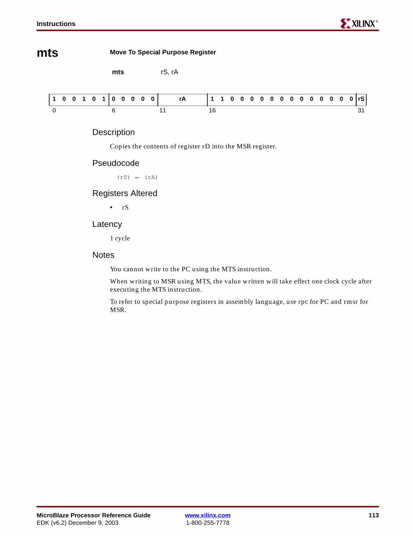
MicroBlaze Processor Reference Guide www.xilinx.com 113EDK (v6.2) December 9, 2003 1-800-255-7778
InstructionsR
mts Move To Special Purpose Register
Description
Copies the contents of register rD into the MSR register.
Pseudocode
(rS) ← (rA)
Registers Altered
• rS
Latency
1 cycle
Notes
You cannot write to the PC using the MTS instruction.
When writing to MSR using MTS, the value written will take effect one clock cycle afterexecuting the MTS instruction.
To refer to special purpose registers in assembly language, use rpc for PC and rmsr forMSR.
mts rS, rA
1 0 0 1 0 1 0 0 0 0 0 rA 1 1 0 0 0 0 0 0 0 0 0 0 0 0 0 rS
0 6 11 16 31
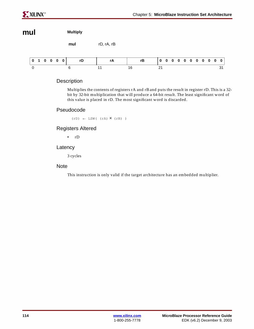
114 www.xilinx.com MicroBlaze Processor Reference Guide1-800-255-7778 EDK (v6.2) December 9, 2003
Chapter 5: MicroBlaze Instruction Set ArchitectureR
mul Multiply
Description
Multiplies the contents of registers rA and rB and puts the result in register rD. This is a 32-bit by 32-bit multiplication that will produce a 64-bit result. The least significant word ofthis value is placed in rD. The most significant word is discarded.
Pseudocode
(rD) ← LSW( (rA) × (rB) )
Registers Altered
• rD
Latency
3 cycles
Note
This instruction is only valid if the target architecture has an embedded multiplier.
mul rD, rA, rB
0 1 0 0 0 0 rD rA rB 0 0 0 0 0 0 0 0 0 0 0
0 6 11 16 21 31
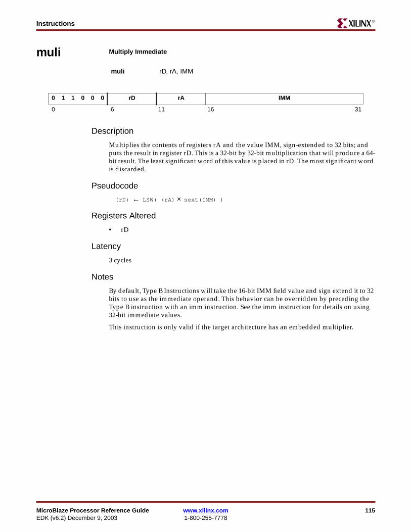
MicroBlaze Processor Reference Guide www.xilinx.com 115EDK (v6.2) December 9, 2003 1-800-255-7778
InstructionsR
muli Multiply Immediate
Description
Multiplies the contents of registers rA and the value IMM, sign-extended to 32 bits; andputs the result in register rD. This is a 32-bit by 32-bit multiplication that will produce a 64-bit result. The least significant word of this value is placed in rD. The most significant wordis discarded.
Pseudocode
(rD) ← LSW( (rA) × sext(IMM) )
Registers Altered
• rD
Latency
3 cycles
Notes
By default, Type B Instructions will take the 16-bit IMM field value and sign extend it to 32bits to use as the immediate operand. This behavior can be overridden by preceding theType B instruction with an imm instruction. See the imm instruction for details on using32-bit immediate values.
This instruction is only valid if the target architecture has an embedded multiplier.
muli rD, rA, IMM
0 1 1 0 0 0 rD rA IMM
0 6 11 16 31
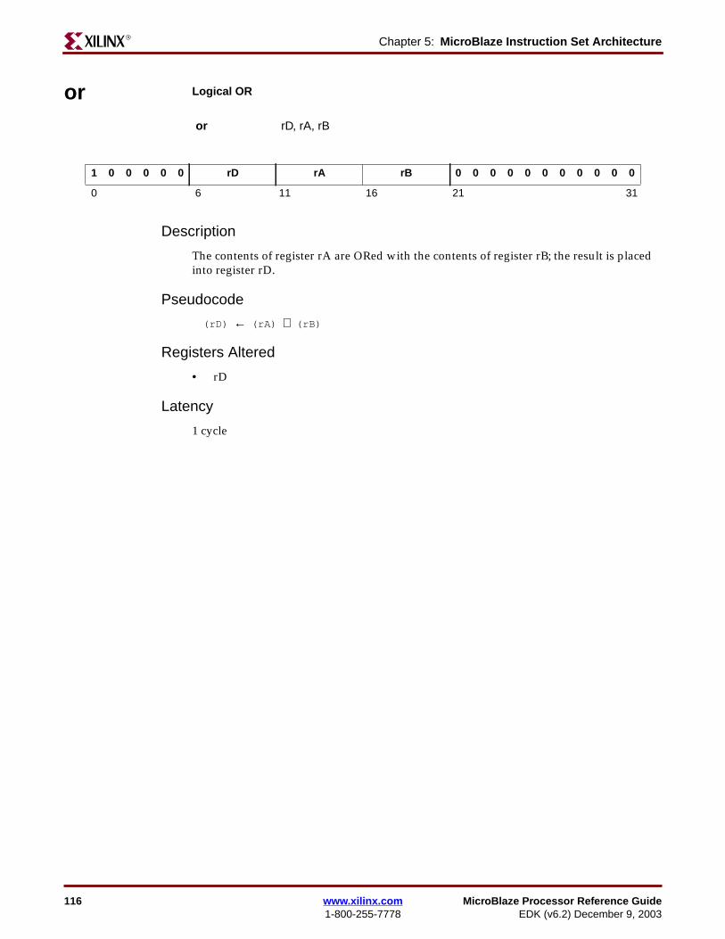
116 www.xilinx.com MicroBlaze Processor Reference Guide1-800-255-7778 EDK (v6.2) December 9, 2003
Chapter 5: MicroBlaze Instruction Set ArchitectureR
or Logical OR
Description
The contents of register rA are ORed with the contents of register rB; the result is placedinto register rD.
Pseudocode
(rD) ← (rA) ∨ (rB)
Registers Altered
• rD
Latency
1 cycle
or rD, rA, rB
1 0 0 0 0 0 rD rA rB 0 0 0 0 0 0 0 0 0 0 0
0 6 11 16 21 31
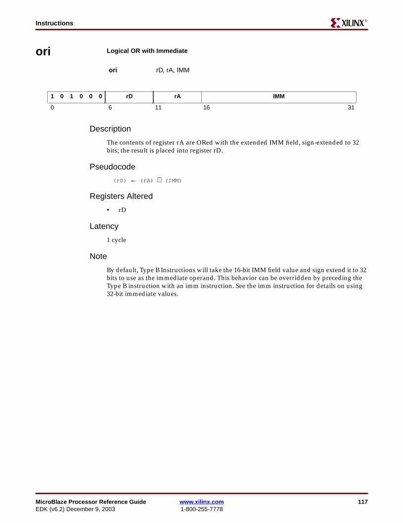
MicroBlaze Processor Reference Guide www.xilinx.com 117EDK (v6.2) December 9, 2003 1-800-255-7778
InstructionsR
ori Logical OR with Immediate
Description
The contents of register rA are ORed with the extended IMM field, sign-extended to 32bits; the result is placed into register rD.
Pseudocode
(rD) ← (rA) ∨ (IMM)
Registers Altered
• rD
Latency
1 cycle
Note
By default, Type B Instructions will take the 16-bit IMM field value and sign extend it to 32bits to use as the immediate operand. This behavior can be overridden by preceding theType B instruction with an imm instruction. See the imm instruction for details on using32-bit immediate values.
ori rD, rA, IMM
1 0 1 0 0 0 rD rA IMM
0 6 11 16 31
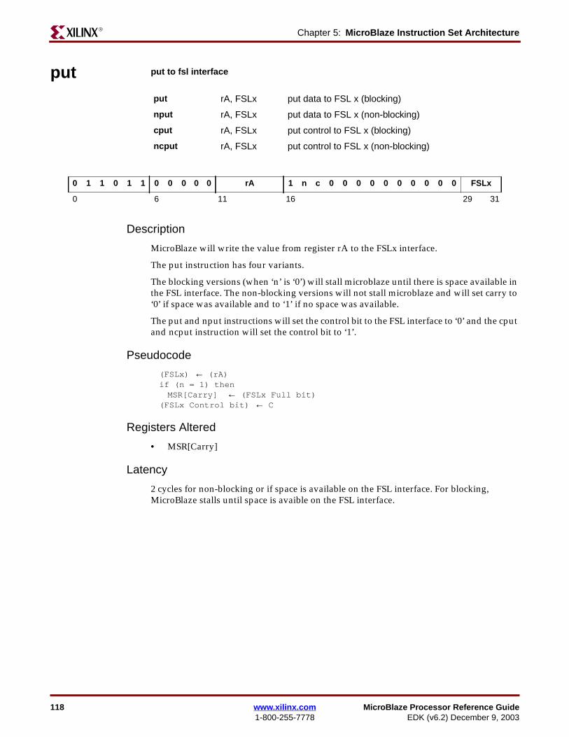
118 www.xilinx.com MicroBlaze Processor Reference Guide1-800-255-7778 EDK (v6.2) December 9, 2003
Chapter 5: MicroBlaze Instruction Set ArchitectureR
put put to fsl interface
Description
MicroBlaze will write the value from register rA to the FSLx interface.
The put instruction has four variants.
The blocking versions (when ‘n’ is ‘0’) will stall microblaze until there is space available inthe FSL interface. The non-blocking versions will not stall microblaze and will set carry to‘0’ if space was available and to ‘1’ if no space was available.
The put and nput instructions will set the control bit to the FSL interface to ‘0’ and the cputand ncput instruction will set the control bit to ‘1’.
Pseudocode
(FSLx) ← (rA)if (n = 1) thenMSR[Carry] ← (FSLx Full bit)
(FSLx Control bit) ← C
Registers Altered
• MSR[Carry]
Latency
2 cycles for non-blocking or if space is available on the FSL interface. For blocking,MicroBlaze stalls until space is avaible on the FSL interface.
put rA, FSLx put data to FSL x (blocking)
nput rA, FSLx put data to FSL x (non-blocking)
cput rA, FSLx put control to FSL x (blocking)
ncput rA, FSLx put control to FSL x (non-blocking)
0 1 1 0 1 1 0 0 0 0 0 rA 1 n c 0 0 0 0 0 0 0 0 0 0 FSLx
0 6 11 16 29 31
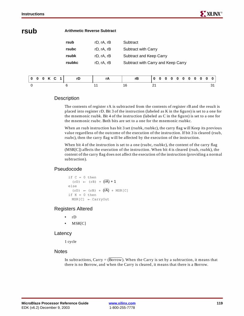
MicroBlaze Processor Reference Guide www.xilinx.com 119EDK (v6.2) December 9, 2003 1-800-255-7778
InstructionsR
rsub Arithmetic Reverse Subtract
Description
The contents of register rA is subtracted from the contents of register rB and the result isplaced into register rD. Bit 3 of the instruction (labeled as K in the figure) is set to a one forthe mnemonic rsubk. Bit 4 of the instruction (labeled as C in the figure) is set to a one forthe mnemonic rsubc. Both bits are set to a one for the mnemonic rsubkc.
When an rsub instruction has bit 3 set (rsubk, rsubkc), the carry flag will Keep its previousvalue regardless of the outcome of the execution of the instruction. If bit 3 is cleared (rsub,rsubc), then the carry flag will be affected by the execution of the instruction.
When bit 4 of the instruction is set to a one (rsubc, rsubkc), the content of the carry flag(MSR[C]) affects the execution of the instruction. When bit 4 is cleared (rsub, rsubk), thecontent of the carry flag does not affect the execution of the instruction (providing a normalsubtraction).
Pseudocode
if C = 0 then(rD) ← (rB) + (rA) + 1
else(rD) ← (rB) + (rA) + MSR[C]
if K = 0 thenMSR[C] ← CarryOut
Registers Altered
• rD
• MSR[C]
Latency
1 cycle
Notes
In subtractions, Carry = (Borrow). When the Carry is set by a subtraction, it means thatthere is no Borrow, and when the Carry is cleared, it means that there is a Borrow.
rsub rD, rA, rB Subtract
rsubc rD, rA, rB Subtract with Carry
rsubk rD, rA, rB Subtract and Keep Carry
rsubkc rD, rA, rB Subtract with Carry and Keep Carry
0 0 0 K C 1 rD rA rB 0 0 0 0 0 0 0 0 0 0 0
0 6 11 16 21 31
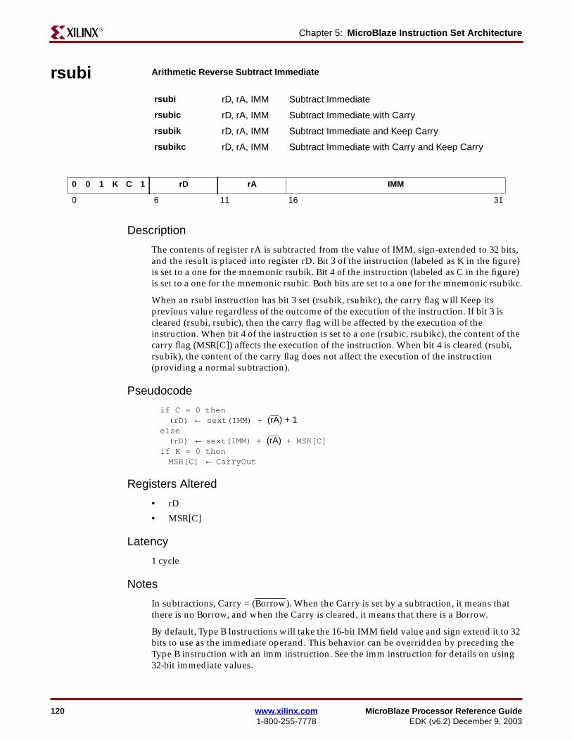
120 www.xilinx.com MicroBlaze Processor Reference Guide1-800-255-7778 EDK (v6.2) December 9, 2003
Chapter 5: MicroBlaze Instruction Set ArchitectureR
rsubi Arithmetic Reverse Subtract Immediate
Description
The contents of register rA is subtracted from the value of IMM, sign-extended to 32 bits,and the result is placed into register rD. Bit 3 of the instruction (labeled as K in the figure)is set to a one for the mnemonic rsubik. Bit 4 of the instruction (labeled as C in the figure)is set to a one for the mnemonic rsubic. Both bits are set to a one for the mnemonic rsubikc.
When an rsubi instruction has bit 3 set (rsubik, rsubikc), the carry flag will Keep itsprevious value regardless of the outcome of the execution of the instruction. If bit 3 iscleared (rsubi, rsubic), then the carry flag will be affected by the execution of theinstruction. When bit 4 of the instruction is set to a one (rsubic, rsubikc), the content of thecarry flag (MSR[C]) affects the execution of the instruction. When bit 4 is cleared (rsubi,rsubik), the content of the carry flag does not affect the execution of the instruction(providing a normal subtraction).
Pseudocode
if C = 0 then(rD) ← sext(IMM) + (rA) + 1
else(rD) ← sext(IMM) + (rA) + MSR[C]
if K = 0 thenMSR[C] ← CarryOut
Registers Altered
• rD
• MSR[C]
Latency
1 cycle
Notes
In subtractions, Carry = (Borrow). When the Carry is set by a subtraction, it means thatthere is no Borrow, and when the Carry is cleared, it means that there is a Borrow.
By default, Type B Instructions will take the 16-bit IMM field value and sign extend it to 32bits to use as the immediate operand. This behavior can be overridden by preceding theType B instruction with an imm instruction. See the imm instruction for details on using32-bit immediate values.
rsubi rD, rA, IMM Subtract Immediate
rsubic rD, rA, IMM Subtract Immediate with Carry
rsubik rD, rA, IMM Subtract Immediate and Keep Carry
rsubikc rD, rA, IMM Subtract Immediate with Carry and Keep Carry
0 0 1 K C 1 rD rA IMM
0 6 11 16 31
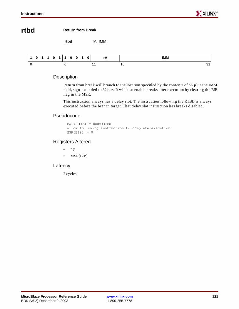
MicroBlaze Processor Reference Guide www.xilinx.com 121EDK (v6.2) December 9, 2003 1-800-255-7778
InstructionsR
rtbd Return from Breakrn from Interrupt
Description
Return from break will branch to the location specified by the contents of rA plus the IMMfield, sign-extended to 32 bits. It will also enable breaks after execution by clearing the BIPflag in the MSR.
This instruction always has a delay slot. The instruction following the RTBD is alwaysexecuted before the branch target. That delay slot instruction has breaks disabled.
Pseudocode
PC ← (rA) + sext(IMM)allow following instruction to complete executionMSR[BIP] ← 0
Registers Altered
• PC
• MSR[BIP]
Latency
2 cycles
rtbd rA, IMM
1 0 1 1 0 1 1 0 0 1 0 rA IMM
0 6 11 16 31
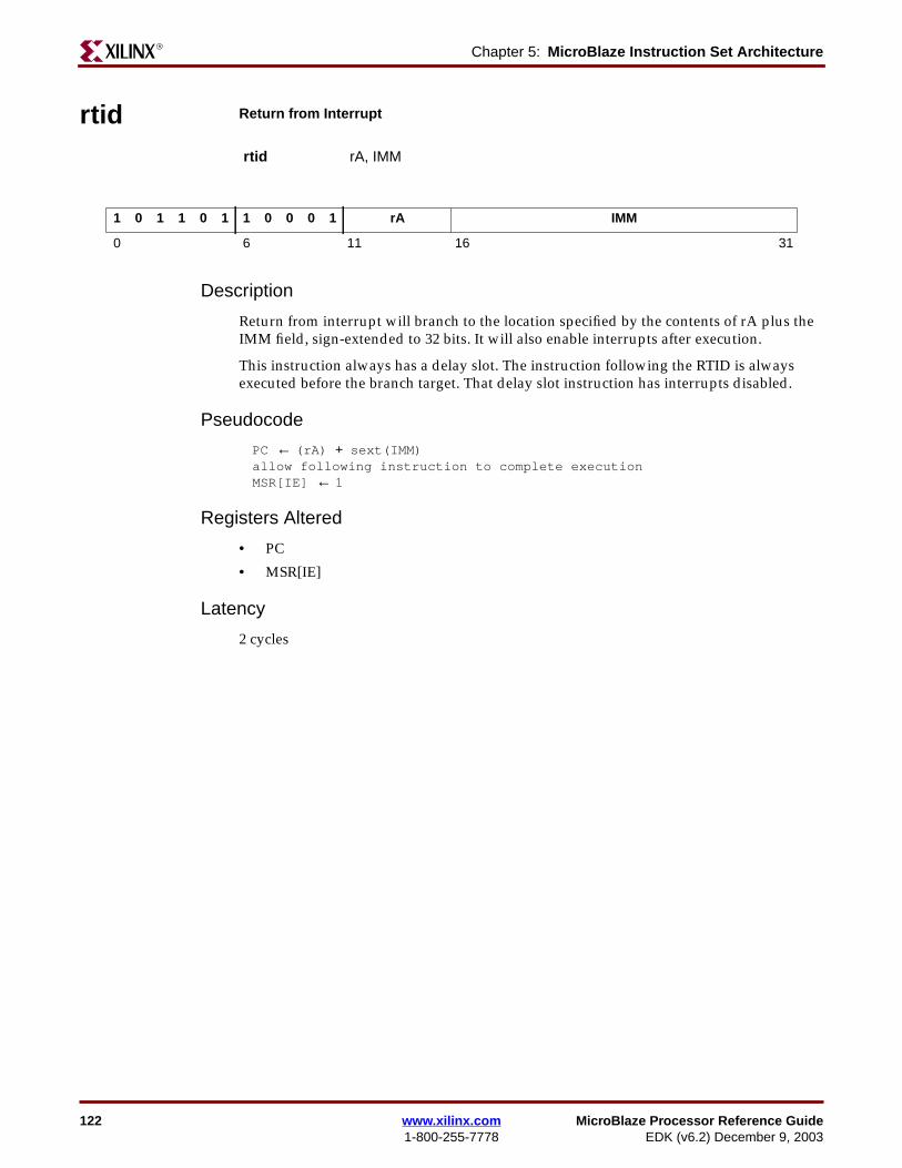
122 www.xilinx.com MicroBlaze Processor Reference Guide1-800-255-7778 EDK (v6.2) December 9, 2003
Chapter 5: MicroBlaze Instruction Set ArchitectureR
rtid Return from Interruptrn from Interrupt
Description
Return from interrupt will branch to the location specified by the contents of rA plus theIMM field, sign-extended to 32 bits. It will also enable interrupts after execution.
This instruction always has a delay slot. The instruction following the RTID is alwaysexecuted before the branch target. That delay slot instruction has interrupts disabled.
Pseudocode
PC ← (rA) + sext(IMM)allow following instruction to complete executionMSR[IE] ← 1
Registers Altered
• PC
• MSR[IE]
Latency
2 cycles
rtid rA, IMM
1 0 1 1 0 1 1 0 0 0 1 rA IMM
0 6 11 16 31
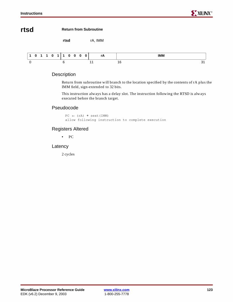
MicroBlaze Processor Reference Guide www.xilinx.com 123EDK (v6.2) December 9, 2003 1-800-255-7778
InstructionsR
rtsd Return from Subroutine
Description
Return from subroutine will branch to the location specified by the contents of rA plus theIMM field, sign-extended to 32 bits.
This instruction always has a delay slot. The instruction following the RTSD is alwaysexecuted before the branch target.
Pseudocode
PC ← (rA) + sext(IMM)allow following instruction to complete execution
Registers Altered
• PC
Latency
2 cycles
rtsd rA, IMM
1 0 1 1 0 1 1 0 0 0 0 rA IMM
0 6 11 16 31
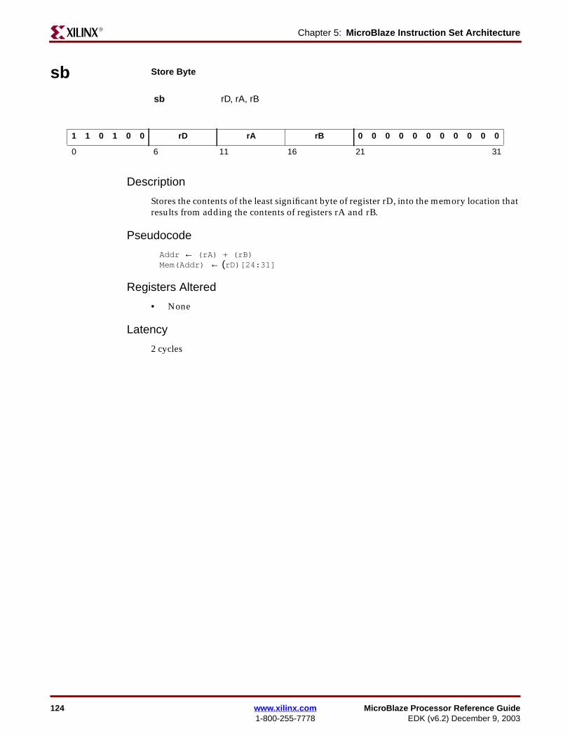
124 www.xilinx.com MicroBlaze Processor Reference Guide1-800-255-7778 EDK (v6.2) December 9, 2003
Chapter 5: MicroBlaze Instruction Set ArchitectureR
sb Store Byte
Description
Stores the contents of the least significant byte of register rD, into the memory location thatresults from adding the contents of registers rA and rB.
Pseudocode
Addr ← (rA) + (rB)Mem(Addr) ← (rD)[24:31]
Registers Altered
• None
Latency
2 cycles
sb rD, rA, rB
1 1 0 1 0 0 rD rA rB 0 0 0 0 0 0 0 0 0 0 0
0 6 11 16 21 31
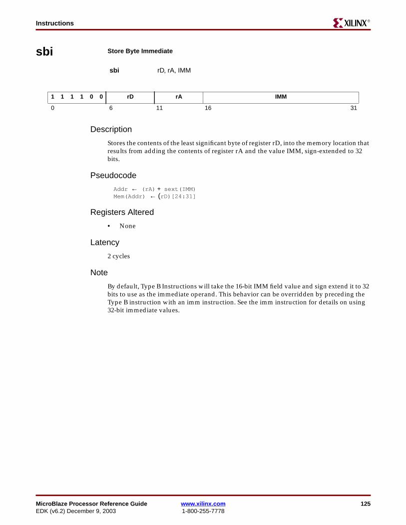
MicroBlaze Processor Reference Guide www.xilinx.com 125EDK (v6.2) December 9, 2003 1-800-255-7778
InstructionsR
sbi Store Byte Immediate
Description
Stores the contents of the least significant byte of register rD, into the memory location thatresults from adding the contents of register rA and the value IMM, sign-extended to 32bits.
Pseudocode
Addr ← (rA) + sext(IMM)Mem(Addr) ← (rD)[24:31]
Registers Altered
• None
Latency
2 cycles
Note
By default, Type B Instructions will take the 16-bit IMM field value and sign extend it to 32bits to use as the immediate operand. This behavior can be overridden by preceding theType B instruction with an imm instruction. See the imm instruction for details on using32-bit immediate values.
sbi rD, rA, IMM
1 1 1 1 0 0 rD rA IMM
0 6 11 16 31
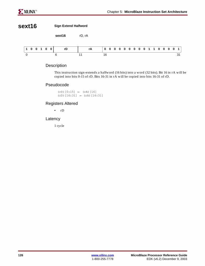
126 www.xilinx.com MicroBlaze Processor Reference Guide1-800-255-7778 EDK (v6.2) December 9, 2003
Chapter 5: MicroBlaze Instruction Set ArchitectureR
sext16 Sign Extend Halfword
Description
This instruction sign-extends a halfword (16 bits) into a word (32 bits). Bit 16 in rA will becopied into bits 0-15 of rD. Bits 16-31 in rA will be copied into bits 16-31 of rD.
Pseudocode
(rD)[0:15] ← (rA)[16](rD)[16:31] ← (rA)[16:31]
Registers Altered
• rD
Latency
1 cycle
sext16 rD, rA
1 0 0 1 0 0 rD rA 0 0 0 0 0 0 0 0 0 1 1 0 0 0 0 1
0 6 11 16 31
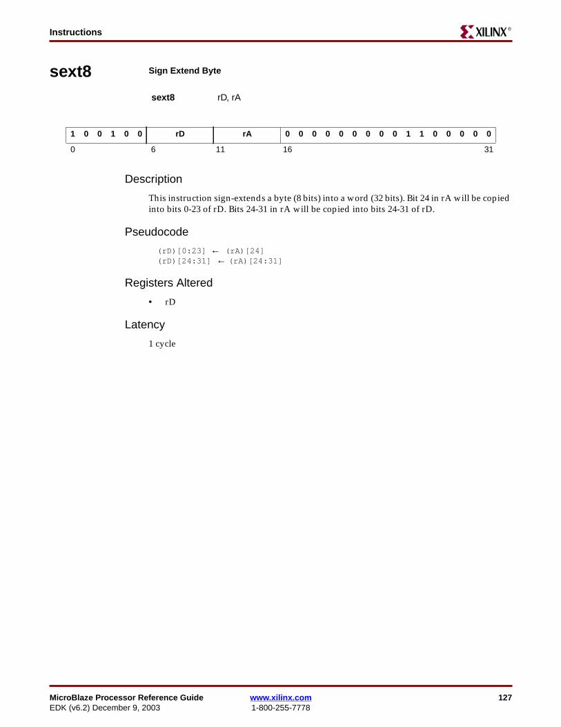
MicroBlaze Processor Reference Guide www.xilinx.com 127EDK (v6.2) December 9, 2003 1-800-255-7778
InstructionsR
sext8 Sign Extend Byte
Description
This instruction sign-extends a byte (8 bits) into a word (32 bits). Bit 24 in rA will be copiedinto bits 0-23 of rD. Bits 24-31 in rA will be copied into bits 24-31 of rD.
Pseudocode
(rD)[0:23] ← (rA)[24](rD)[24:31] ← (rA)[24:31]
Registers Altered
• rD
Latency
1 cycle
sext8 rD, rA
1 0 0 1 0 0 rD rA 0 0 0 0 0 0 0 0 0 1 1 0 0 0 0 0
0 6 11 16 31

128 www.xilinx.com MicroBlaze Processor Reference Guide1-800-255-7778 EDK (v6.2) December 9, 2003
Chapter 5: MicroBlaze Instruction Set ArchitectureR
sh Store Halfword
Description
Stores the contents of the least significant halfword of register rD, into the halfwordaligned memory location that results from adding the contents of registers rA and rB.
Pseudocode
Addr ← (rA) + (rB)Addr[31] ← 0Mem(Addr) ← (rD)[16:31]
Registers Altered
• None
Latency
2 cycles
sh rD, rA, rB
1 1 0 1 0 1 rD rA rB 0 0 0 0 0 0 0 0 0 0 0
0 6 11 16 21 31
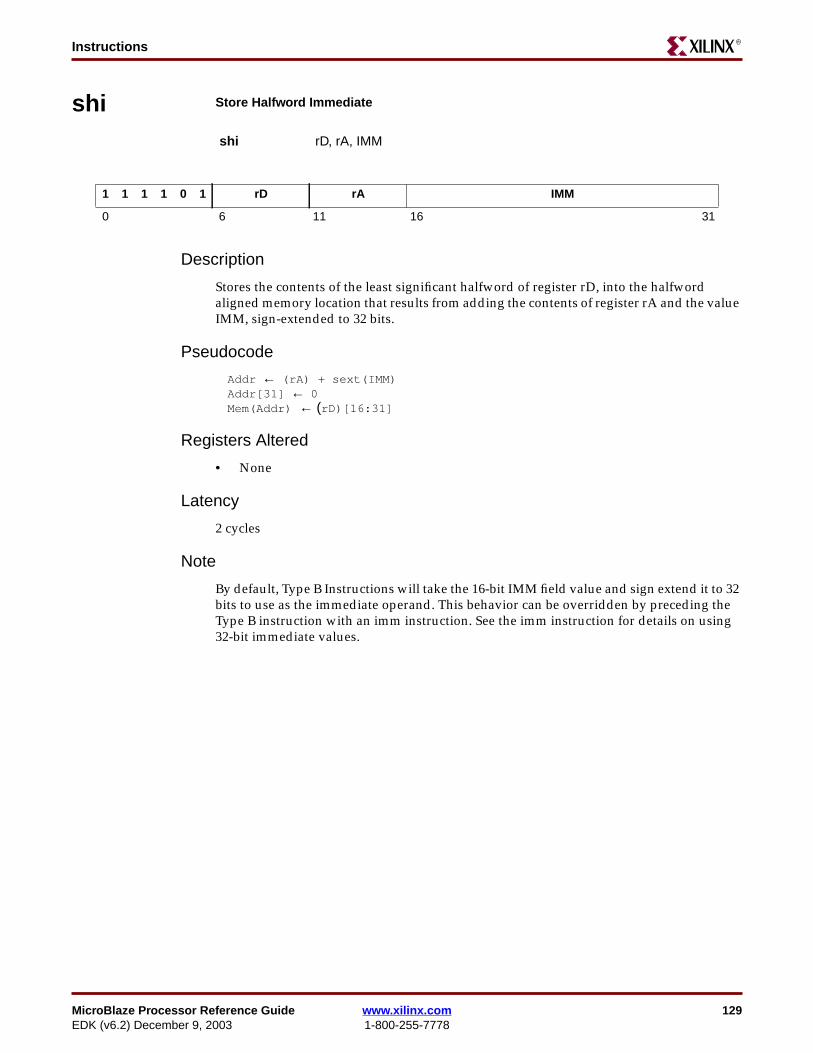
MicroBlaze Processor Reference Guide www.xilinx.com 129EDK (v6.2) December 9, 2003 1-800-255-7778
InstructionsR
shi Store Halfword Immediate
Description
Stores the contents of the least significant halfword of register rD, into the halfwordaligned memory location that results from adding the contents of register rA and the valueIMM, sign-extended to 32 bits.
Pseudocode
Addr ← (rA) + sext(IMM)Addr[31] ← 0Mem(Addr) ← (rD)[16:31]
Registers Altered
• None
Latency
2 cycles
Note
By default, Type B Instructions will take the 16-bit IMM field value and sign extend it to 32bits to use as the immediate operand. This behavior can be overridden by preceding theType B instruction with an imm instruction. See the imm instruction for details on using32-bit immediate values.
shi rD, rA, IMM
1 1 1 1 0 1 rD rA IMM
0 6 11 16 31
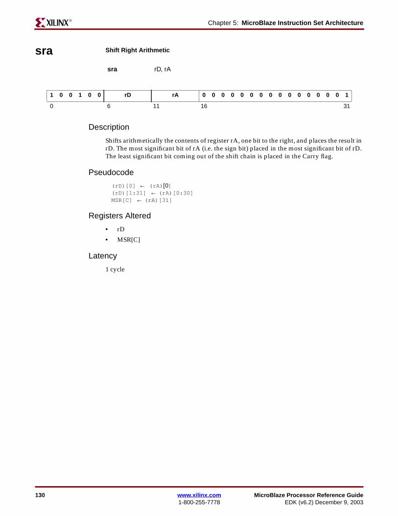
130 www.xilinx.com MicroBlaze Processor Reference Guide1-800-255-7778 EDK (v6.2) December 9, 2003
Chapter 5: MicroBlaze Instruction Set ArchitectureR
sra Shift Right Arithmetic
Description
Shifts arithmetically the contents of register rA, one bit to the right, and places the result inrD. The most significant bit of rA (i.e. the sign bit) placed in the most significant bit of rD.The least significant bit coming out of the shift chain is placed in the Carry flag.
Pseudocode
(rD)[0] ← (rA)[0](rD)[1:31] ← (rA)[0:30]MSR[C] ← (rA)[31]
Registers Altered
• rD
• MSR[C]
Latency
1 cycle
sra rD, rA
1 0 0 1 0 0 rD rA 0 0 0 0 0 0 0 0 0 0 0 0 0 0 0 1
0 6 11 16 31
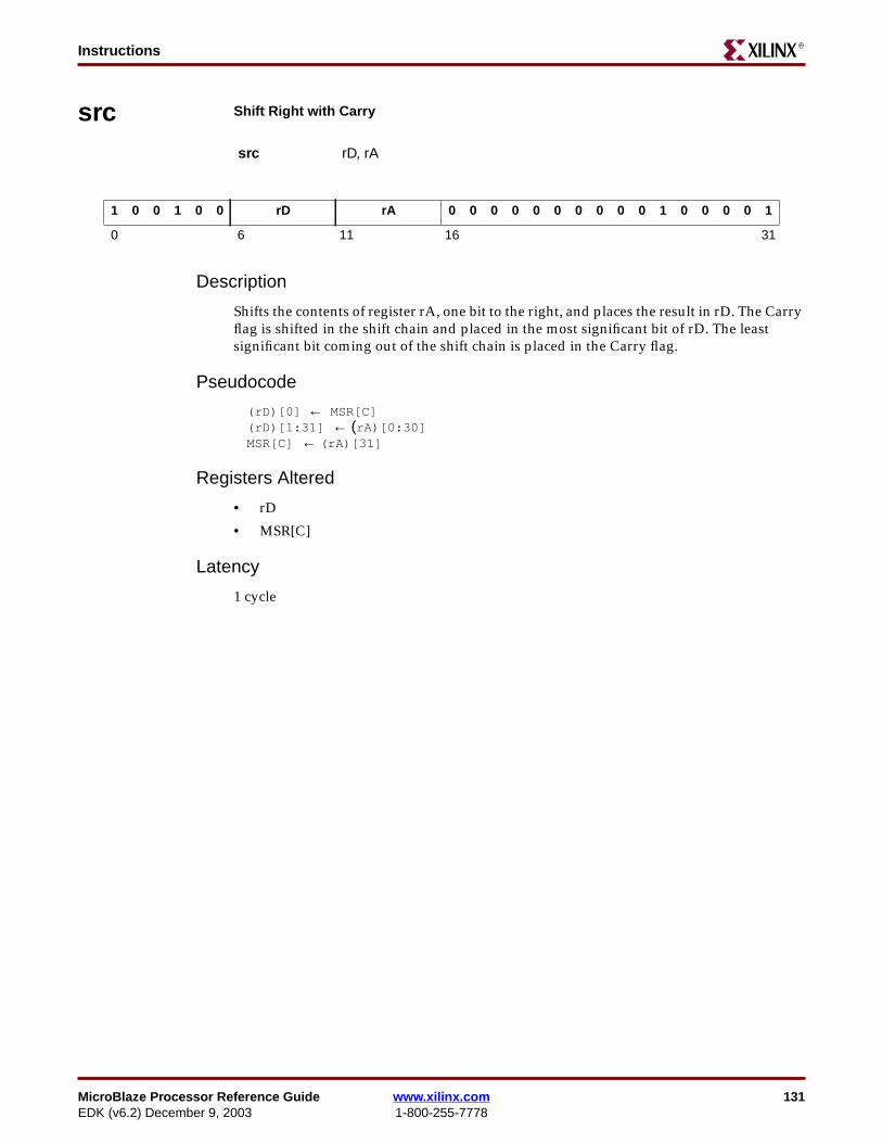
MicroBlaze Processor Reference Guide www.xilinx.com 131EDK (v6.2) December 9, 2003 1-800-255-7778
InstructionsR
src Shift Right with Carry
Description
Shifts the contents of register rA, one bit to the right, and places the result in rD. The Carryflag is shifted in the shift chain and placed in the most significant bit of rD. The leastsignificant bit coming out of the shift chain is placed in the Carry flag.
Pseudocode
(rD)[0] ← MSR[C](rD)[1:31] ← (rA)[0:30]MSR[C] ← (rA)[31]
Registers Altered
• rD
• MSR[C]
Latency
1 cycle
src rD, rA
1 0 0 1 0 0 rD rA 0 0 0 0 0 0 0 0 0 0 1 0 0 0 0 1
0 6 11 16 31

132 www.xilinx.com MicroBlaze Processor Reference Guide1-800-255-7778 EDK (v6.2) December 9, 2003
Chapter 5: MicroBlaze Instruction Set ArchitectureR
srl Shift Right Logical
Description
Shifts logically the contents of register rA, one bit to the right, and places the result in rD.A zero is shifted in the shift chain and placed in the most significant bit of rD. The leastsignificant bit coming out of the shift chain is placed in the Carry flag.
Pseudocode
(rD)[0] ← 0(rD)[1:31] ← (rA)[0:30]MSR[C] ← (rA)[31]
Registers Altered
• rD
• MSR[C]
Latency
1 cycle
srl rD, rA
1 0 0 1 0 0 rD rA 0 0 0 0 0 0 0 0 0 1 0 0 0 0 0 1
0 6 11 16 31
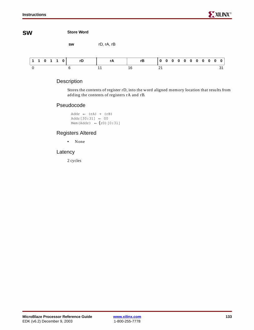
MicroBlaze Processor Reference Guide www.xilinx.com 133EDK (v6.2) December 9, 2003 1-800-255-7778
InstructionsR
sw Store Word
Description
Stores the contents of register rD, into the word aligned memory location that results fromadding the contents of registers rA and rB.
Pseudocode
Addr ← (rA) + (rB)Addr[30:31] ← 00Mem(Addr) ← (rD)[0:31]
Registers Altered
• None
Latency
2 cycles
sw rD, rA, rB
1 1 0 1 1 0 rD rA rB 0 0 0 0 0 0 0 0 0 0 0
0 6 11 16 21 31
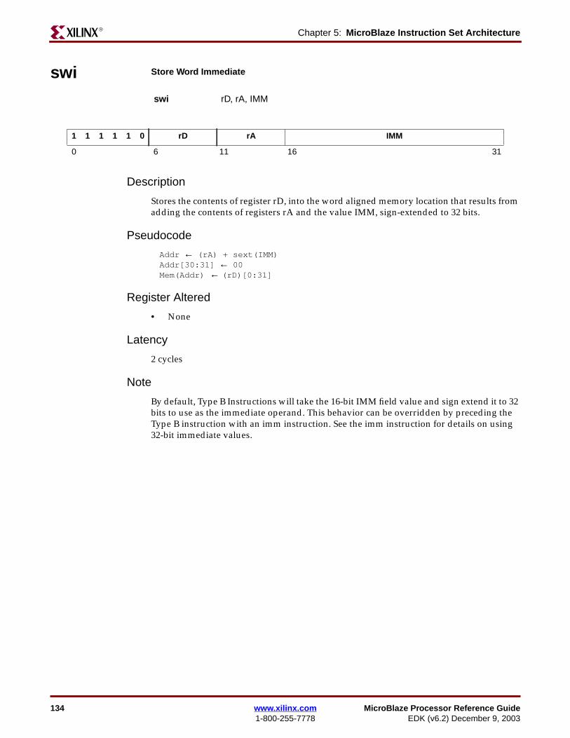
134 www.xilinx.com MicroBlaze Processor Reference Guide1-800-255-7778 EDK (v6.2) December 9, 2003
Chapter 5: MicroBlaze Instruction Set ArchitectureR
swi Store Word Immediate
Description
Stores the contents of register rD, into the word aligned memory location that results fromadding the contents of registers rA and the value IMM, sign-extended to 32 bits.
Pseudocode
Addr ← (rA) + sext(IMM)Addr[30:31] ← 00Mem(Addr) ← (rD)[0:31]
Register Altered
• None
Latency
2 cycles
Note
By default, Type B Instructions will take the 16-bit IMM field value and sign extend it to 32bits to use as the immediate operand. This behavior can be overridden by preceding theType B instruction with an imm instruction. See the imm instruction for details on using32-bit immediate values.
swi rD, rA, IMM
1 1 1 1 1 0 rD rA IMM
0 6 11 16 31
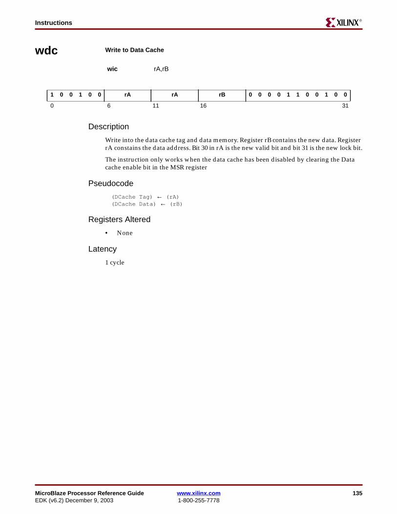
MicroBlaze Processor Reference Guide www.xilinx.com 135EDK (v6.2) December 9, 2003 1-800-255-7778
InstructionsR
wdc Write to Data Cache
Description
Write into the data cache tag and data memory. Register rB contains the new data. RegisterrA constains the data address. Bit 30 in rA is the new valid bit and bit 31 is the new lock bit.
The instruction only works when the data cache has been disabled by clearing the Datacache enable bit in the MSR register
Pseudocode
(DCache Tag) ← (rA)(DCache Data) ← (rB)
Registers Altered
• None
Latency
1 cycle
wic rA,rB
1 0 0 1 0 0 rA rA rB 0 0 0 0 1 1 0 0 1 0 0
0 6 11 16 31
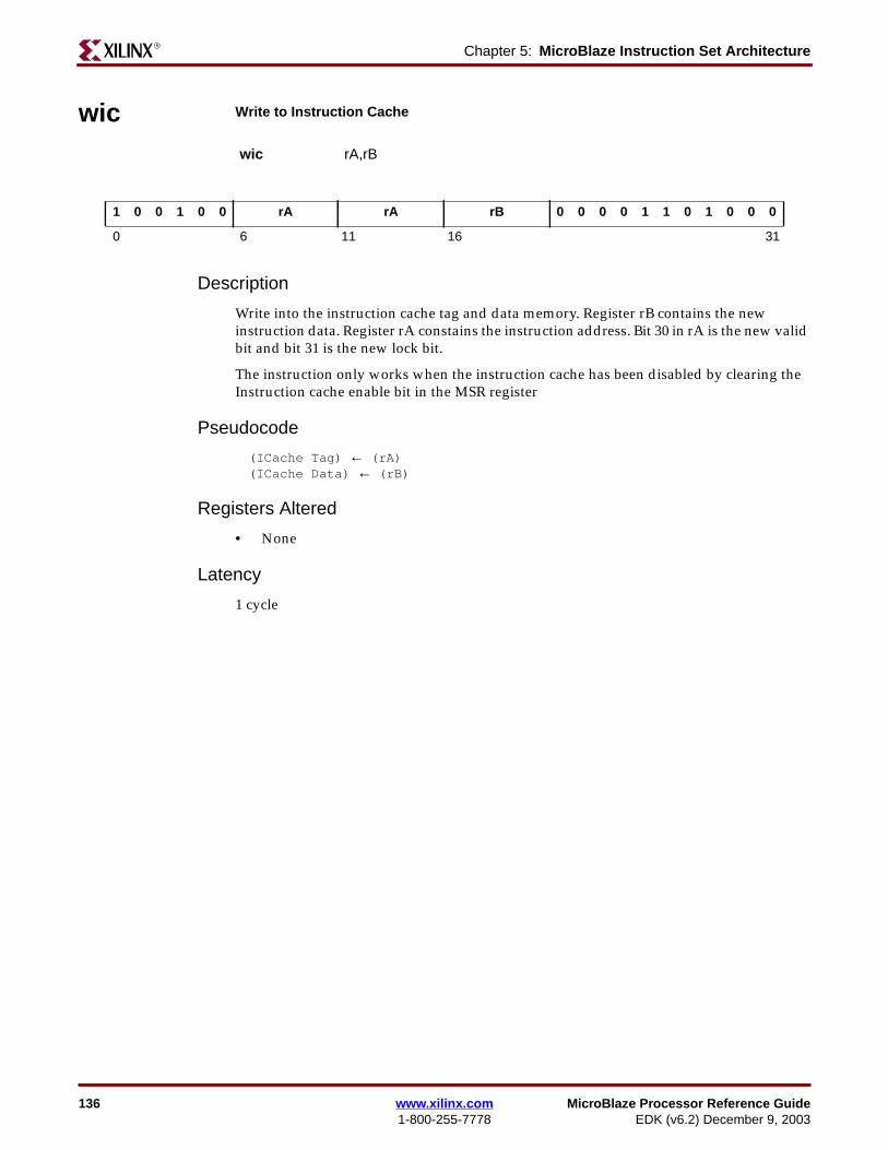
136 www.xilinx.com MicroBlaze Processor Reference Guide1-800-255-7778 EDK (v6.2) December 9, 2003
Chapter 5: MicroBlaze Instruction Set ArchitectureR
wic Write to Instruction Cache
Description
Write into the instruction cache tag and data memory. Register rB contains the newinstruction data. Register rA constains the instruction address. Bit 30 in rA is the new validbit and bit 31 is the new lock bit.
The instruction only works when the instruction cache has been disabled by clearing theInstruction cache enable bit in the MSR register
Pseudocode
(ICache Tag) ← (rA)(ICache Data) ← (rB)
Registers Altered
• None
Latency
1 cycle
wic rA,rB
1 0 0 1 0 0 rA rA rB 0 0 0 0 1 1 0 1 0 0 0
0 6 11 16 31
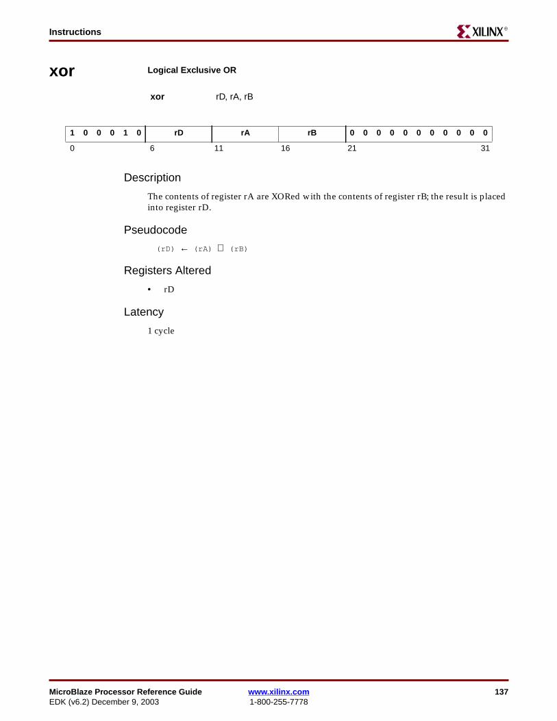
MicroBlaze Processor Reference Guide www.xilinx.com 137EDK (v6.2) December 9, 2003 1-800-255-7778
InstructionsR
xor Logical Exclusive OR
Description
The contents of register rA are XORed with the contents of register rB; the result is placedinto register rD.
Pseudocode
(rD) ← (rA) ⊕ (rB)
Registers Altered
• rD
Latency
1 cycle
xor rD, rA, rB
1 0 0 0 1 0 rD rA rB 0 0 0 0 0 0 0 0 0 0 0
0 6 11 16 21 31
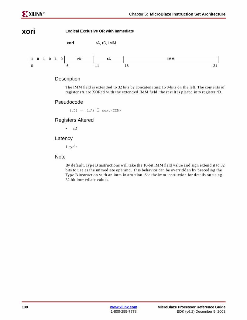
138 www.xilinx.com MicroBlaze Processor Reference Guide1-800-255-7778 EDK (v6.2) December 9, 2003
Chapter 5: MicroBlaze Instruction Set ArchitectureR
xori Logical Exclusive OR with Immediate
Description
The IMM field is extended to 32 bits by concatenating 16 0-bits on the left. The contents ofregister rA are XORed with the extended IMM field; the result is placed into register rD.
Pseudocode
(rD) ← (rA) ⊕ sext(IMM)
Registers Altered
• rD
Latency
1 cycle
Note
By default, Type B Instructions will take the 16-bit IMM field value and sign extend it to 32bits to use as the immediate operand. This behavior can be overridden by preceding theType B instruction with an imm instruction. See the imm instruction for details on using32-bit immediate values.
xori rA, rD, IMM
1 0 1 0 1 0 rD rA IMM
0 6 11 16 31
Recommended