Introduction toCMOS VLSI
Design
Lecture 9: Circuit Families
David Harris
Harvey Mudd CollegeSpring 2004
9: Circuit Families Slide 2CMOS VLSI Design
Outlineq Pseudo-nMOS Logicq Dynamic Logicq Pass Transistor Logic
9: Circuit Families Slide 3CMOS VLSI Design
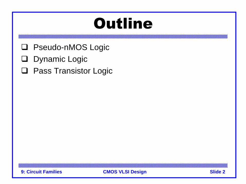
Introductionq What makes a circuit fast?
– I = C dV/dt -> tpd ∝ (C/I) ∆V– low capacitance– high current– small swing
q Logical effort is proportional to C/Iq pMOS are the enemy!
– High capacitance for a given currentq Can we take the pMOS capacitance off the input?q Various circuit families try to do this…
B
A
11
4
4
Y
9: Circuit Families Slide 4CMOS VLSI Design
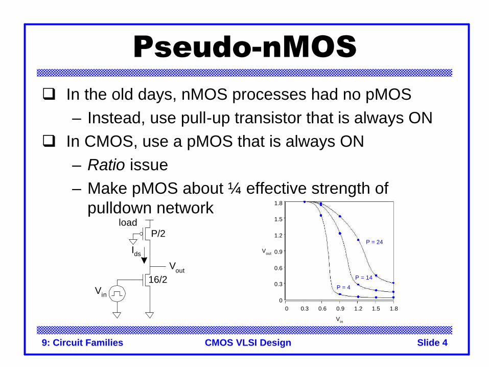
Pseudo-nMOSq In the old days, nMOS processes had no pMOS
– Instead, use pull-up transistor that is always ONq In CMOS, use a pMOS that is always ON
– Ratio issue– Make pMOS about ¼ effective strength of
pulldown network
Vout
Vin
16/2
P/2
Ids
load
0 0.3 0.6 0.9 1.2 1.5 1.80
0.3
0.6
0.9
1.2
1.5
1.8
P = 24
P = 4
P = 14
Vin
Vout
9: Circuit Families Slide 5CMOS VLSI Design
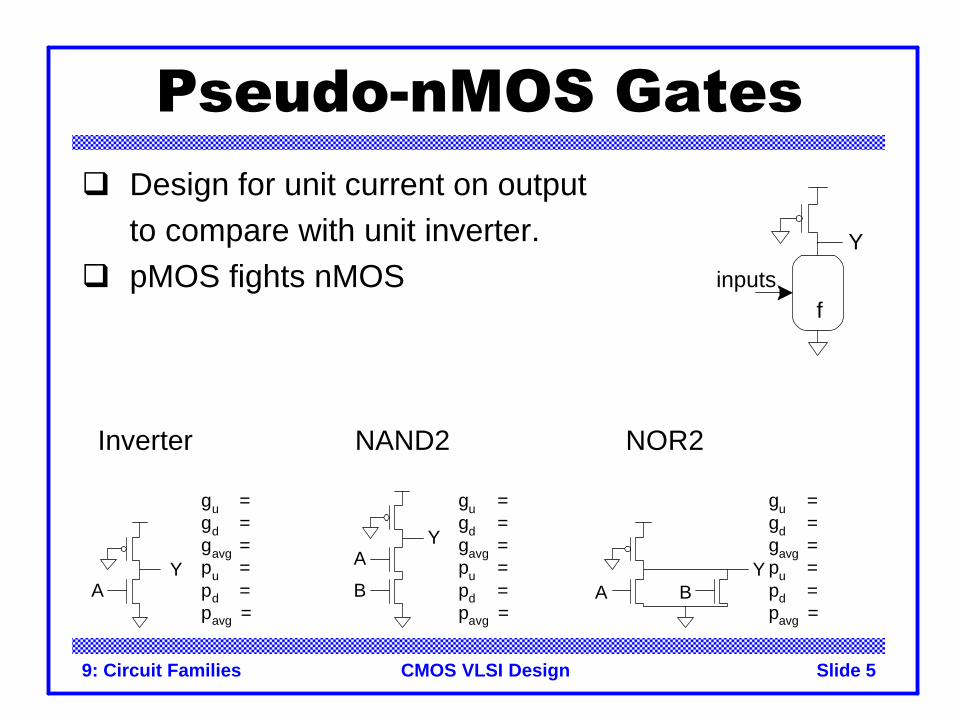
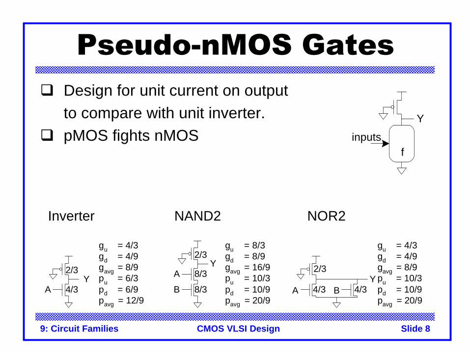
Pseudo-nMOS Gatesq Design for unit current on output
to compare with unit inverter.q pMOS fights nMOS
Inverter NAND2 NOR2
AY
B
AY
A B
gu =gd =gavg =pu =pd =pavg =
Y
gu =gd =gavg =pu =pd =pavg =
gu =gd =gavg =pu =pd =pavg =
finputs
Y
9: Circuit Families Slide 6CMOS VLSI Design
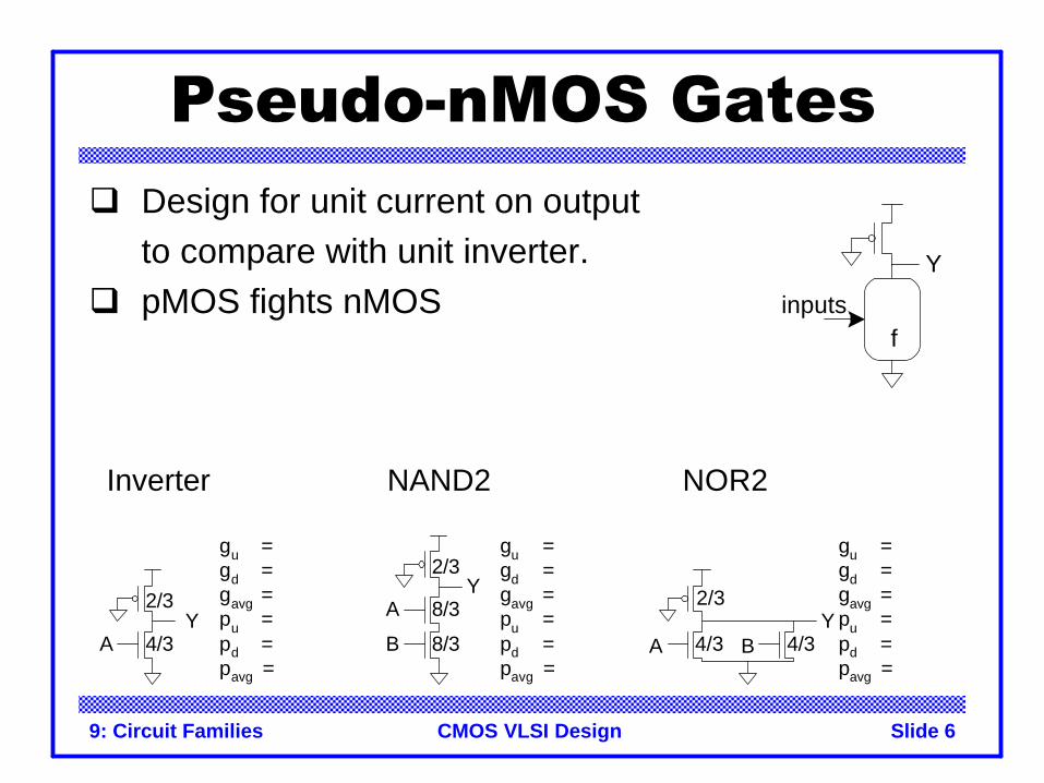
Pseudo-nMOS Gatesq Design for unit current on output
to compare with unit inverter.q pMOS fights nMOS
Inverter NAND2 NOR2
4/3
2/3
AY
8/3
8/3
2/3
B
AY
A B 4/34/3
2/3
gu =gd =gavg =pu =pd =pavg =
Y
gu =gd =gavg =pu =pd =pavg =
gu =gd =gavg =pu =pd =pavg =
finputs
Y
9: Circuit Families Slide 7CMOS VLSI Design
Pseudo-nMOS Gatesq Design for unit current on output
to compare with unit inverter.q pMOS fights nMOS
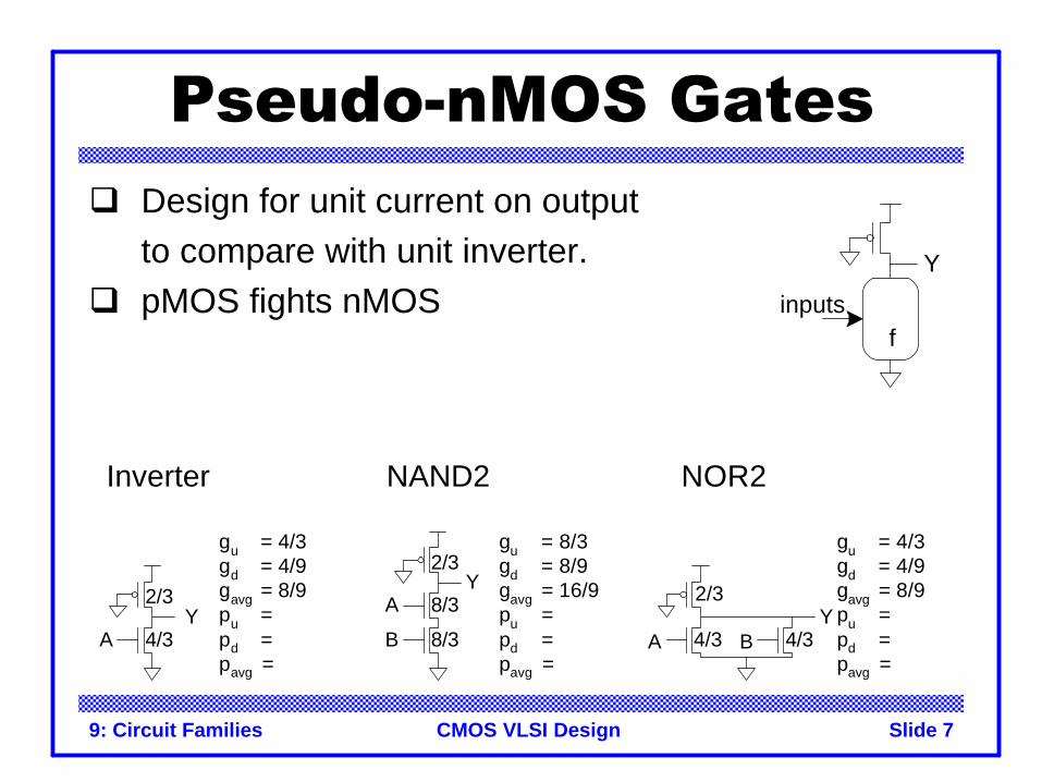
Inverter NAND2 NOR2
4/3
2/3
AY
8/3
8/3
2/3
B
AY
A B 4/34/3
2/3
gu = 4/3gd = 4/9gavg = 8/9pu =pd =pavg =
Y
gu = 8/3gd = 8/9gavg = 16/9pu =pd =pavg =
gu = 4/3gd = 4/9gavg = 8/9pu =pd =pavg =
finputs
Y
9: Circuit Families Slide 8CMOS VLSI Design
Pseudo-nMOS Gatesq Design for unit current on output
to compare with unit inverter.q pMOS fights nMOS
Inverter NAND2 NOR2
4/3
2/3
AY
8/3
8/3
2/3
B
AY
A B 4/34/3
2/3
gu = 4/3gd = 4/9gavg = 8/9pu = 6/3pd = 6/9pavg = 12/9
Y
gu = 8/3gd = 8/9gavg = 16/9pu = 10/3pd = 10/9pavg = 20/9
gu = 4/3gd = 4/9gavg = 8/9pu = 10/3pd = 10/9pavg = 20/9
finputs
Y
9: Circuit Families Slide 9CMOS VLSI Design
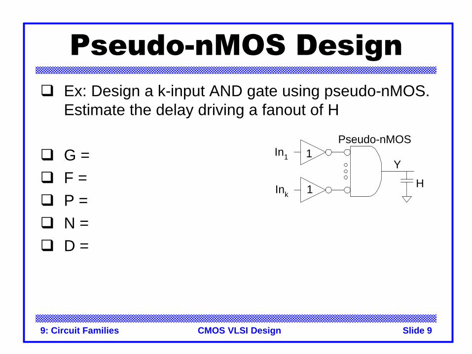
Pseudo-nMOS Designq Ex: Design a k-input AND gate using pseudo-nMOS.
Estimate the delay driving a fanout of H
q G = q F =q P =q N =q D =
In1
Ink
Y
Pseudo-nMOS1
1 H
9: Circuit Families Slide 10CMOS VLSI Design
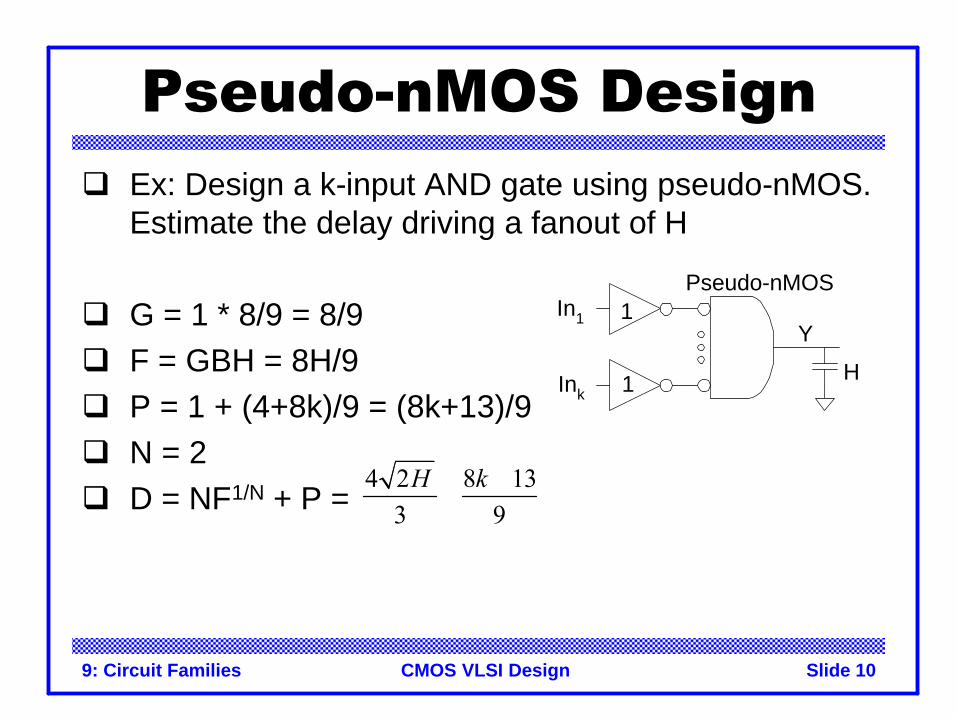
Pseudo-nMOS Designq Ex: Design a k-input AND gate using pseudo-nMOS.
Estimate the delay driving a fanout of H
q G = 1 * 8/9 = 8/9q F = GBH = 8H/9q P = 1 + (4+8k)/9 = (8k+13)/9q N = 2q D = NF1/N + P =
In1
Ink
Y
Pseudo-nMOS1
1 H
4 2 8 133 9
H k ++
9: Circuit Families Slide 11CMOS VLSI Design
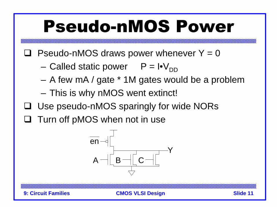
Pseudo-nMOS Powerq Pseudo-nMOS draws power whenever Y = 0
– Called static power P = I•VDD
– A few mA / gate * 1M gates would be a problem– This is why nMOS went extinct!
q Use pseudo-nMOS sparingly for wide NORsq Turn off pMOS when not in use
A BY
C
en
9: Circuit Families Slide 12CMOS VLSI Design
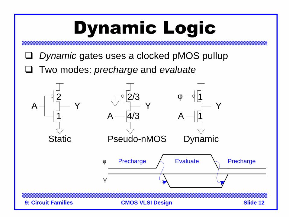
Dynamic Logicq Dynamic gates uses a clocked pMOS pullupq Two modes: precharge and evaluate
1
2A Y
4/3
2/3
AY
1
1
AY
φ
Static Pseudo-nMOS Dynamic
φ Precharge Evaluate
Y
Precharge
9: Circuit Families Slide 13CMOS VLSI Design
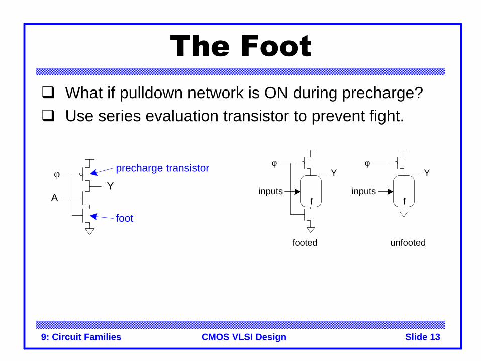
The Footq What if pulldown network is ON during precharge?q Use series evaluation transistor to prevent fight.
AY
φ
foot
precharge transistor φY
inputs
φY
inputs
footed unfooted
f f
9: Circuit Families Slide 14CMOS VLSI Design
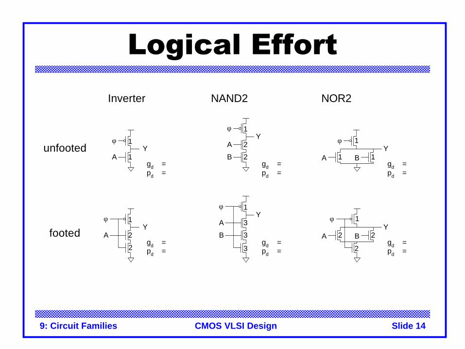
Logical EffortInverter NAND2 NOR2
1
1
AY
2
2
1
B
AY
A B 11
1
gd =pd =
gd =pd =
gd =pd =
Yφ
φ
φ
2
1
AY
3
3
1
B
AY
A B 22
1
gd =pd =
gd =pd =
gd =pd =
Yφ
φ
φ
footed
unfooted
32 2
9: Circuit Families Slide 15CMOS VLSI Design
Logical EffortInverter NAND2 NOR2
1
1
AY
2
2
1
B
AY
A B 11
1
gd = 1/3pd = 2/3
gd = 2/3pd = 3/3
gd = 1/3pd = 3/3
Yφ
φ
φ
2
1
AY
3
3
1
B
AY
A B 22
1
gd = 2/3pd = 3/3
gd = 3/3pd = 4/3
gd = 2/3pd = 5/3
Yφ
φ
φ
footed
unfooted
32 2
9: Circuit Families Slide 16CMOS VLSI Design
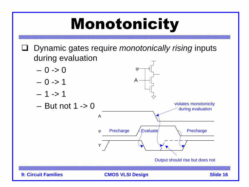
Monotonicityq Dynamic gates require monotonically rising inputs
during evaluation– 0 -> 0– 0 -> 1– 1 -> 1– But not 1 -> 0
φ Precharge Evaluate
Y
Precharge
A
Output should rise but does not
violates monotonicity during evaluation
A
φ
9: Circuit Families Slide 17CMOS VLSI Design
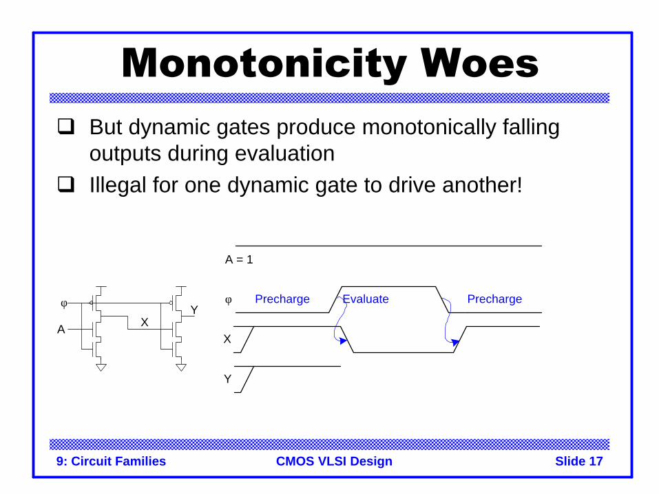
Monotonicity Woesq But dynamic gates produce monotonically falling
outputs during evaluationq Illegal for one dynamic gate to drive another!
A X
φY
φ Precharge Evaluate
X
Precharge
A = 1
Y
9: Circuit Families Slide 18CMOS VLSI Design
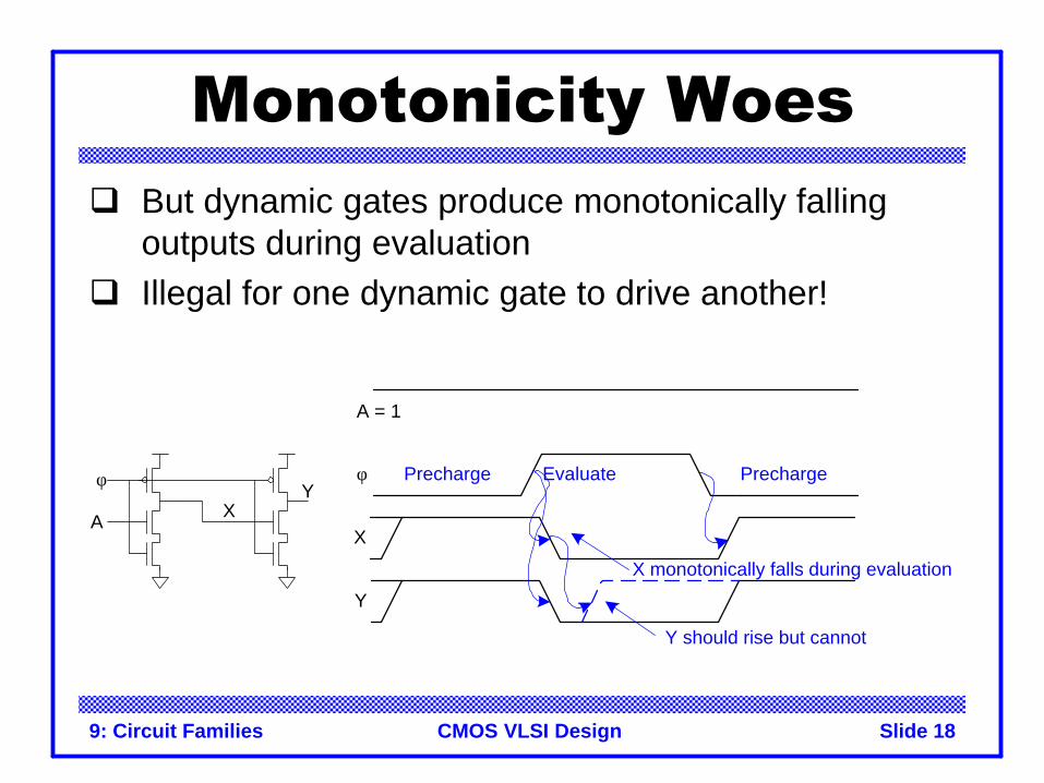
Monotonicity Woesq But dynamic gates produce monotonically falling
outputs during evaluationq Illegal for one dynamic gate to drive another!
A X
φY
φ Precharge Evaluate
X
Precharge
A = 1
Y should rise but cannot
Y
X monotonically falls during evaluation
9: Circuit Families Slide 19CMOS VLSI Design
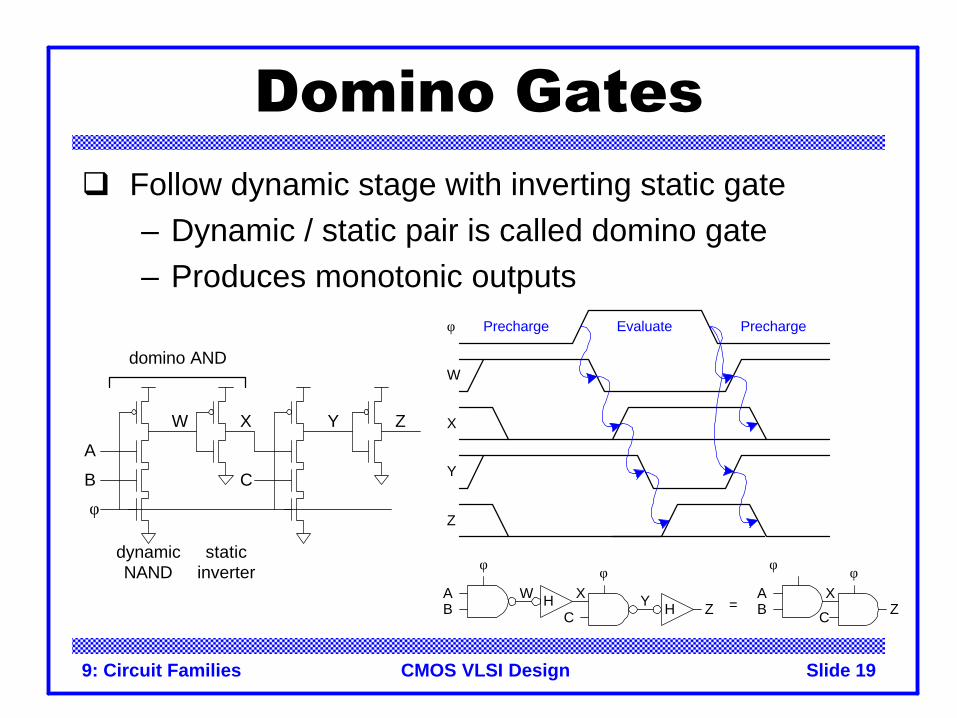
Domino Gatesq Follow dynamic stage with inverting static gate
– Dynamic / static pair is called domino gate– Produces monotonic outputs
φ Precharge Evaluate
W
Precharge
X
Y
Z
A
φ
B C
φ φ φ
C
AB
W X Y Z =X
ZH H
A
W
φ
B C
X Y Z
domino AND
dynamicNAND
staticinverter
9: Circuit Families Slide 20CMOS VLSI Design
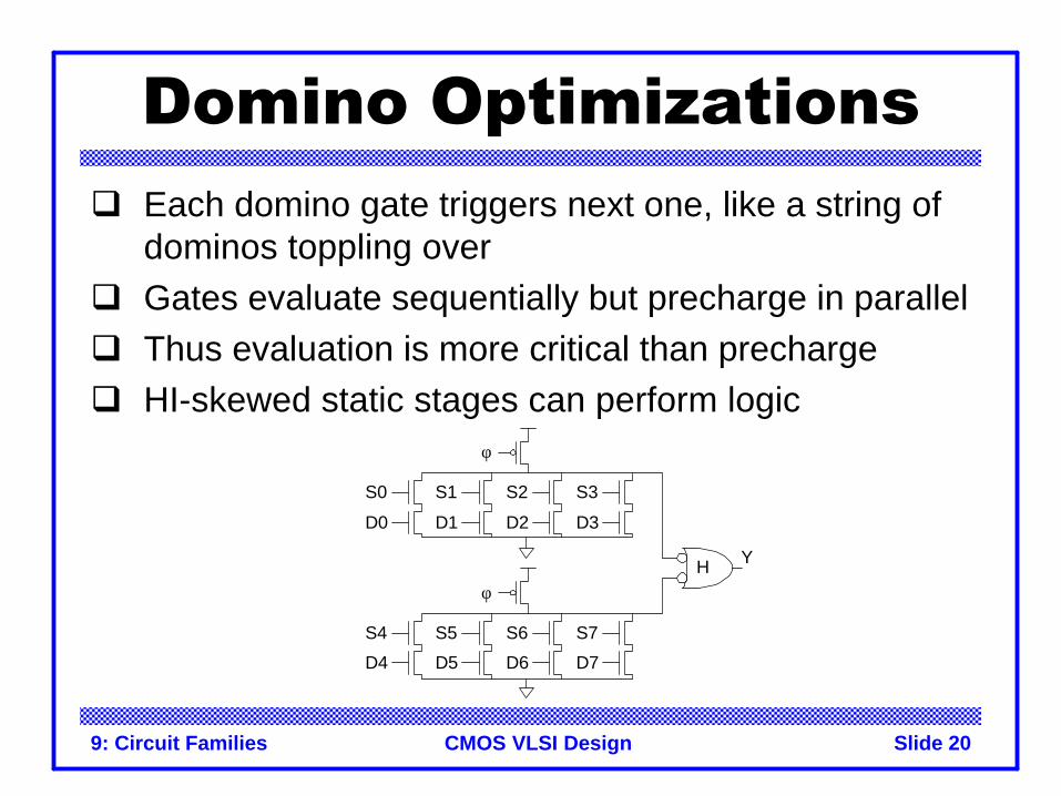
Domino Optimizationsq Each domino gate triggers next one, like a string of
dominos toppling overq Gates evaluate sequentially but precharge in parallelq Thus evaluation is more critical than prechargeq HI-skewed static stages can perform logic
S0
D0
S1
D1
S2
D2
S3
D3
φ
S4
D4
S5
D5
S6
D6
S7
D7
φ
YH
9: Circuit Families Slide 21CMOS VLSI Design
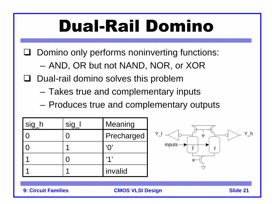
Dual-Rail Dominoq Domino only performs noninverting functions:
– AND, OR but not NAND, NOR, or XORq Dual-rail domino solves this problem
– Takes true and complementary inputs – Produces true and complementary outputs
invalid11
‘1’01
‘0’10
Precharged00
Meaningsig_lsig_hY_h
f
φ
φ
inputs
Y_l
f
9: Circuit Families Slide 22CMOS VLSI Design
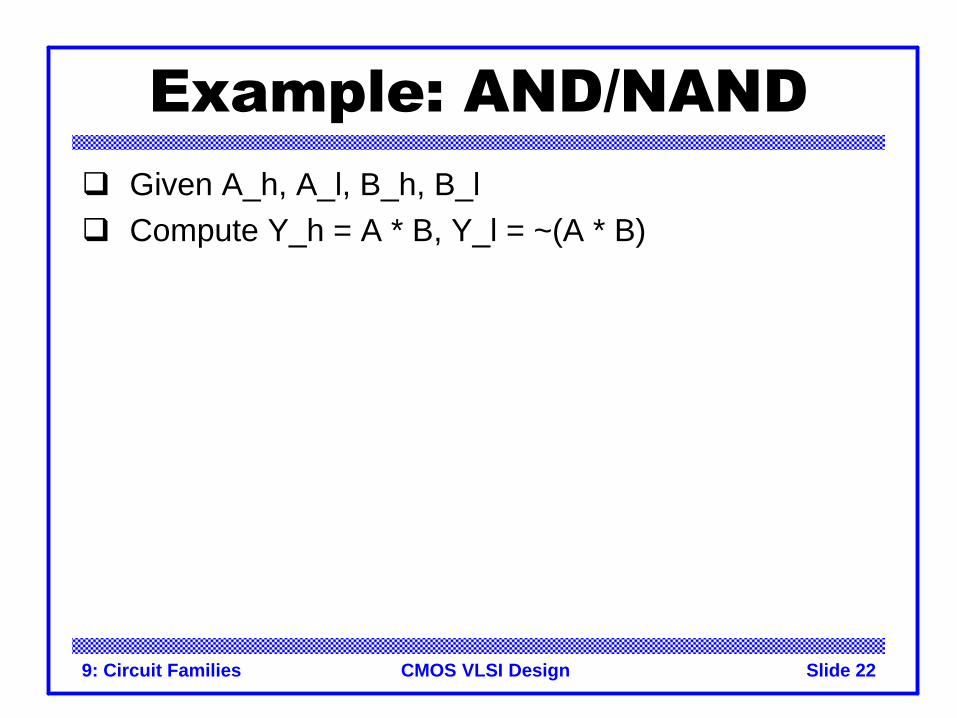
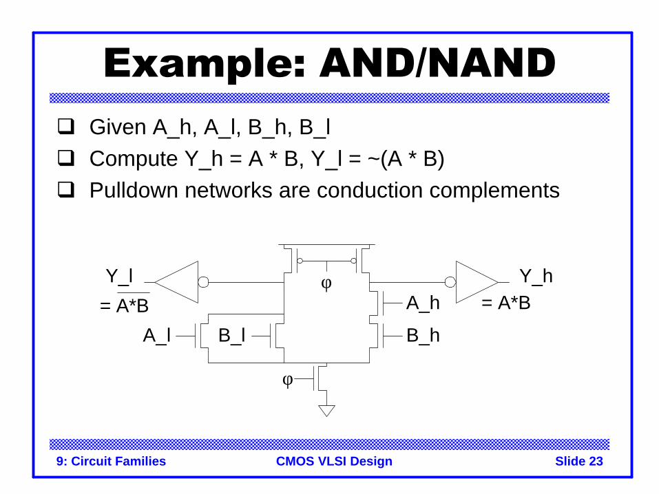
Example: AND/NANDq Given A_h, A_l, B_h, B_lq Compute Y_h = A * B, Y_l = ~(A * B)
9: Circuit Families Slide 23CMOS VLSI Design
Example: AND/NANDq Given A_h, A_l, B_h, B_lq Compute Y_h = A * B, Y_l = ~(A * B)q Pulldown networks are conduction complements
Y_hφ
φ
Y_lA_h
B_hB_lA_l
= A*B= A*B
9: Circuit Families Slide 24CMOS VLSI Design
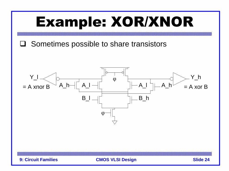
Example: XOR/XNORq Sometimes possible to share transistors
Y_hφ
φ
Y_lA_l
B_h
= A xor B
B_l
A_hA_lA_h= A xnor B
9: Circuit Families Slide 25CMOS VLSI Design
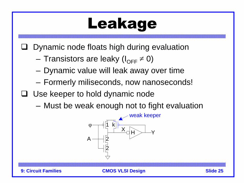
Leakageq Dynamic node floats high during evaluation
– Transistors are leaky (IOFF ≠ 0)– Dynamic value will leak away over time– Formerly miliseconds, now nanoseconds!
q Use keeper to hold dynamic node– Must be weak enough not to fight evaluation
A
φH
2
2
1 kX Y
weak keeper
9: Circuit Families Slide 26CMOS VLSI Design
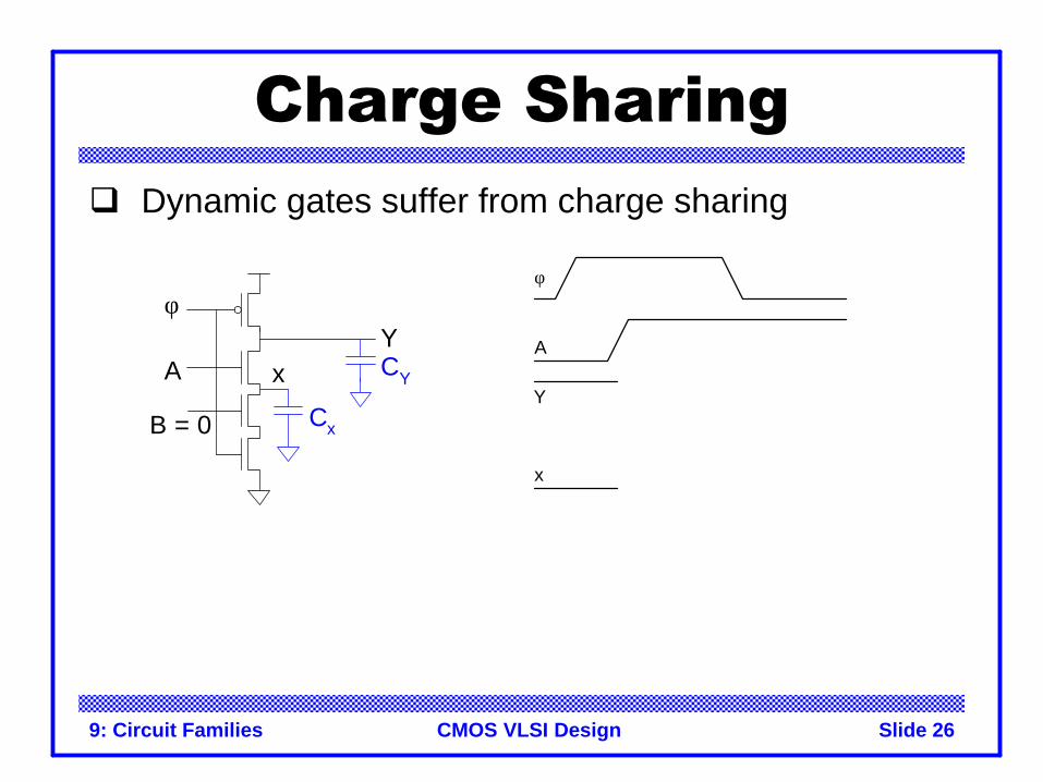
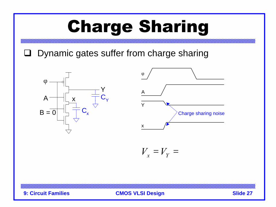
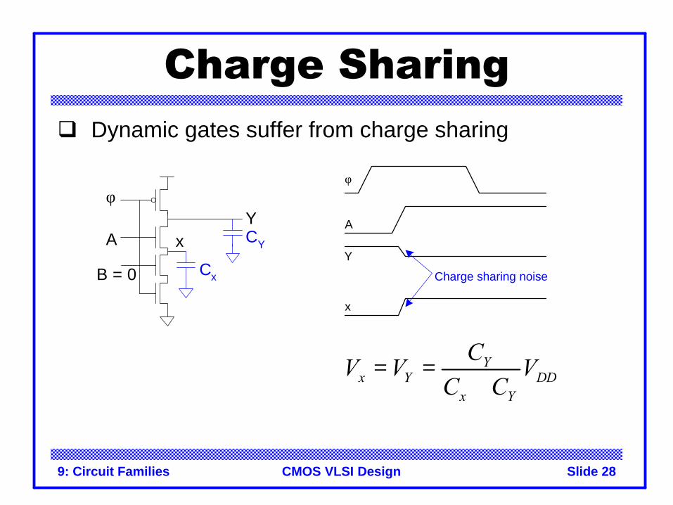
Charge Sharingq Dynamic gates suffer from charge sharing
B = 0
AY
φ
x
Cx
CY
A
φ
x
Y
9: Circuit Families Slide 27CMOS VLSI Design
Charge Sharingq Dynamic gates suffer from charge sharing
B = 0
AY
φ
x
Cx
CY
A
φ
x
Y
Charge sharing noise
x YV V= =
9: Circuit Families Slide 28CMOS VLSI Design
Charge Sharingq Dynamic gates suffer from charge sharing
B = 0
AY
φ
x
Cx
CY
A
φ
x
Y
Charge sharing noise
Yx Y DD
x Y
CV V V
C C= =
+
9: Circuit Families Slide 29CMOS VLSI Design
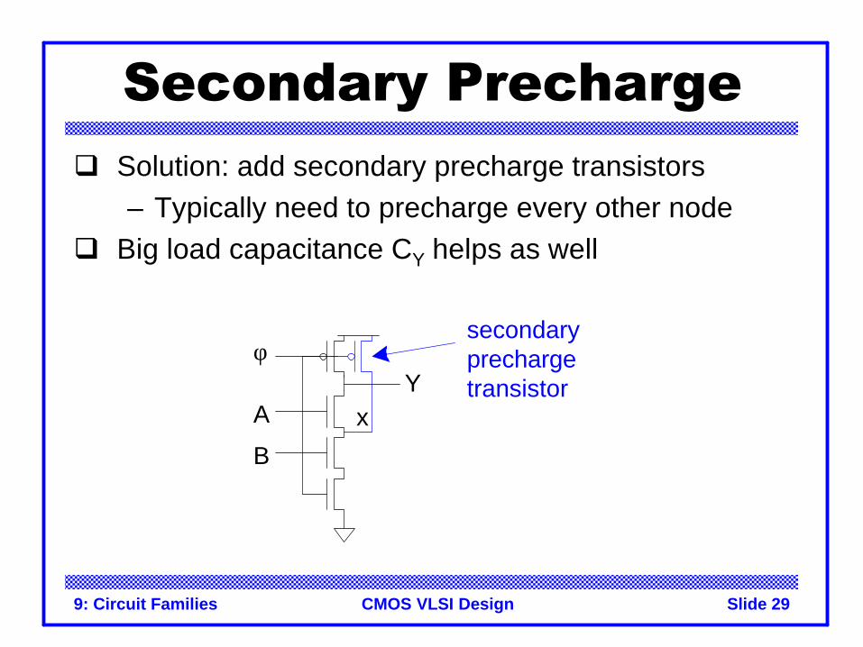
Secondary Prechargeq Solution: add secondary precharge transistors
– Typically need to precharge every other nodeq Big load capacitance CY helps as well
B
AY
φ
x
secondaryprechargetransistor
9: Circuit Families Slide 30CMOS VLSI Design
Noise Sensitivityq Dynamic gates are very sensitive to noise
– Inputs: VIH ≈ Vtn
– Outputs: floating output susceptible noiseq Noise sources
– Capacitive crosstalk– Charge sharing– Power supply noise– Feedthrough noise– And more!
9: Circuit Families Slide 31CMOS VLSI Design
Domino Summaryq Domino logic is attractive for high-speed circuits
– 1.5 – 2x faster than static CMOS– But many challenges:
• Monotonicity• Leakage• Charge sharing• Noise
q Widely used in high-performance microprocessors
9: Circuit Families Slide 32CMOS VLSI Design
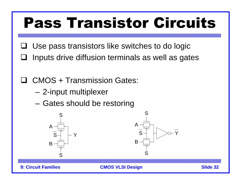
Pass Transistor Circuitsq Use pass transistors like switches to do logicq Inputs drive diffusion terminals as well as gates
q CMOS + Transmission Gates:– 2-input multiplexer– Gates should be restoring
A
B
S
S
S
Y
A
B
S
S
S
Y
9: Circuit Families Slide 33CMOS VLSI Design
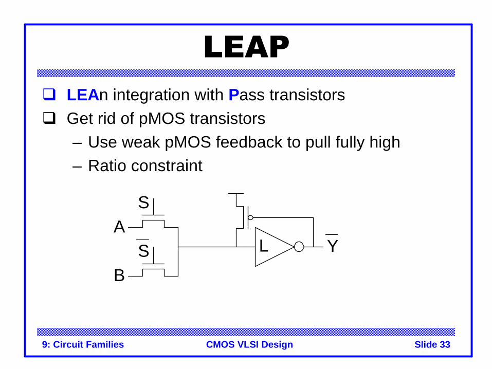
LEAPq LEAn integration with Pass transistorsq Get rid of pMOS transistors
– Use weak pMOS feedback to pull fully high– Ratio constraint
B
S
SA
YL
9: Circuit Families Slide 34CMOS VLSI Design
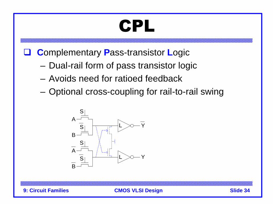
CPLq Complementary Pass-transistor Logic
– Dual-rail form of pass transistor logic– Avoids need for ratioed feedback– Optional cross-coupling for rail-to-rail swing
B
S
S
S
S
A
B
AY
YL
L
Recommended