Document Number: 313685-004
Intel® Core™2 Duo Desktop Processor, Intel® Pentium® Dual Core Processor, and Intel® Pentium® 4 Processor 6x1 Δ Sequence Thermal and Mechanical Design Guidelines – Supporting the Intel® Core™2 Duo desktop processor
E6000 Δ and E4000 Δ sequences, Intel® Pentium® Dual Core Processor E2000 Δ sequence, and Intel® Pentium® 4 processor 6x1 sequence at 65 W
June 2007

2 Thermal and Mechanical Design Guidelines
THIS DOCUMENT AND RELATED MATERIALS AND INFORMATION ARE PROVIDED “AS IS” WITH NO WARRANTIES, EXPRESS OR IMPLIED, INCLUDING BUT NOT LIMITED TO ANY IMPLIED WARRANTY OF MERCHANTABILITY, FITNESS FOR A PARTICULAR PURPOSE, NON-INFRINGEMENT OF INTELLECTUAL PROPERTY RIGHTS, OR ANY WARRANTY OTHERWISE ARISING OUT OF ANY PROPOSAL, SPECIFICATION, OR SAMPLE. INTEL ASSUMES NO RESPONSIBILITY FOR ANY ERRORS CONTAINED IN THIS DOCUMENT AND HAS NO LIABILITIES OR OBLIGATIONS FOR ANY DAMAGES ARISING FROM OR IN CONNECTION WITH THE USE OF THIS DOCUMENT. Intel products are not intended for use in medical, life saving, life sustaining, critical control or safety systems, or in nuclear facility applications.
Intel Corporation may have patents or pending patent applications, trademarks, copyrights, or other intellectual property rights that relate to the presented subject matter. The furnishing of documents and other materials and information does not provide any license, express or implied, by estoppel or otherwise, to any such patents, trademarks, copyrights, or other intellectual property rights.
Intel may make changes to specifications and product descriptions at any time, without notice. Intel accepts no duty to update specifications or product descriptions with information. Designers must not rely on the absence or characteristics of any features or instructions marked “reserved” or “undefined.” Intel reserves these for future definition and shall have no responsibility whatsoever for conflicts or incompatibilities arising from future changes to them.
The hardware vendor remains solely responsible for the design, sale and functionality of its product, including any liability arising from product infringement or product warranty. Intel provides this information for customer’s convenience only. Use at your own risk. Intel accepts no liability for results if customer chooses at its discretion to implement these methods within its business operations. Intel makes no representations or warranties regarding the accuracy or completeness of the information provided.
Copies of documents which have an order number and are referenced in this document, or other Intel literature, may be obtained by calling 1-800-548-4725, or by visiting http://www.intel.com .
The Intel® Core™2 Duo desktop processor E6000/E4000 sequence, Intel® Pentium® Dual Core Processor E2000 sequence, and Intel® Pentium® 4 Processor 6x1 sequence may contain design defects or errors known as errata, which may cause the product to deviate from published specifications. Current characterized errata are available on request. ∆Intel processor numbers are not a measure of performance. Processor numbers differentiate features within each processor family, not across different processor families. Over time processor numbers will increment based on changes in clock, speed, cache, FSB, or other features, and increments are not intended to represent proportional or quantitative increases in any particular feature. Current roadmap processor number progression is not necessarily representative of future roadmaps. See www.intel.com/products/processor_number for details.
Intel, Pentium, Intel Core, Intel Inside, and the Intel logo are trademarks of Intel Corporation in the U.S. and other countries.
*Other names and brands may be claimed as the property of others.
Copyright © 2006–2007 Intel Corporation

Thermal and Mechanical Design Guidelines 3
Contents 1 Introduction ...................................................................................................11
1.1 Document Goals and Scope ...................................................................11 1.1.1 Importance of Thermal Management ..........................................11 1.1.2 Document Goals......................................................................11 1.1.3 Document Scope .....................................................................12
1.2 References ..........................................................................................13 1.3 Definition of Terms ...............................................................................13
2 Processor Thermal/Mechanical Information .........................................................15 2.1 Mechanical Requirements ......................................................................15
2.1.1 Processor Package...................................................................15 2.1.2 Heatsink Attach ......................................................................17
2.2 Thermal Requirements ..........................................................................18 2.2.1 Processor Case Temperature.....................................................18 2.2.2 Thermal Profile .......................................................................19 2.2.3 TCONTROL..................................................................................20
2.3 Heatsink Design Considerations..............................................................21 2.3.1 Heatsink Size..........................................................................22 2.3.2 Heatsink Mass.........................................................................22 2.3.3 Package IHS Flatness...............................................................23 2.3.4 Thermal Interface Material........................................................23
2.4 System Thermal Solution Considerations .................................................24 2.4.1 Chassis Thermal Design Capabilities...........................................24 2.4.2 Improving Chassis Thermal Performance ....................................24 2.4.3 Summary...............................................................................25
2.5 System Integration Considerations..........................................................25 3 Thermal Metrology ..........................................................................................27
3.1 Characterizing Cooling Performance Requirements ....................................27 3.1.1 Example ................................................................................28
3.2 Processor Thermal Solution Performance Assessment ................................29 3.3 Local Ambient Temperature Measurement Guidelines.................................30 3.4 Processor Case Temperature Measurement Guidelines ...............................32
4 Thermal Management Logic and Thermal Monitor Feature .....................................33 4.1 Processor Power Dissipation...................................................................33 4.2 Thermal Monitor Implementation ............................................................33
4.2.1 Prochot# Signal ......................................................................34 4.2.2 Thermal Control Circuit ............................................................34 4.2.3 Thermal Monitor 2 ...................................................................35 4.2.4 Operation and Configuration .....................................................36 4.2.5 On-Demand Mode ...................................................................37 4.2.6 System Considerations.............................................................37 4.2.7 Operating System and Application Software Considerations ...........38 4.2.8 THERMTRIP# Signal.................................................................38 4.2.9 Cooling System Failure Warning ................................................38

4 Thermal and Mechanical Design Guidelines
4.2.10 Digital Thermal Sensor.............................................................39 4.2.11 Platform Environmental Control Interface (PECI)..........................40
5 Intel® Enabled Balanced Technology Extended (BTX) Reference solution .................41 5.1 Overview of the Balanced Technology Extended (BTX) Reference Design ......41
5.1.1 Target Heatsink Performance ....................................................41 5.1.2 Acoustics ...............................................................................42 5.1.3 Effective Fan Curve .................................................................43 5.1.4 Voltage Regulator Thermal Management.....................................44 5.1.5 Altitude..................................................................................45 5.1.6 Reference Heatsink Thermal Validation .......................................45 5.1.7 Fan Performance for Active Heatsink Thermal Solution..................45
5.2 Environmental Reliability Testing ............................................................46 5.2.1 Structural Reliability Testing .....................................................46 5.2.2 Power Cycling .........................................................................48 5.2.3 Recommended BIOS/Processor/Memory Test Procedures ..............48
5.3 Material and Recycling Requirements ......................................................48 5.4 Safety Requirements ............................................................................49 5.5 Geometric Envelope for Intel® Reference Balanced Technology
Extended (BTX) Thermal Module Assembly...............................................49 5.6 Preload and TMA Stiffness .....................................................................50
5.6.1 Structural Design Strategy........................................................50 5.6.2 TMA Preload vs. Stiffness .........................................................50
6 ATX Thermal/Mechanical Design Information.......................................................53 6.1 ATX Reference Design Requirements .......................................................53
6.1.1 Target Heatsink Performance ....................................................53 6.1.2 Acoustics ...............................................................................54 6.1.3 Altitude..................................................................................55 6.1.4 Heatsink Thermal Validation .....................................................55 6.1.5 Fan Performance for Active Heatsink Thermal Solution..................55
6.2 Environmental Reliability Testing ............................................................56 6.2.1 Structural Reliability Testing .....................................................56 6.2.2 Power Cycling .........................................................................58 6.2.3 Recommended BIOS/Processor/Memory Test Procedures ..............59
6.3 Material and Recycling Requirements ......................................................59 6.4 Safety Requirements ............................................................................60 6.5 Geometric Envelope for Intel® Reference ATX Thermal Mechanical Design ....60 6.6 Reference Attach Mechanism..................................................................61
6.6.1 Structural Design Strategy........................................................61 6.6.2 Mechanical Interface to the Reference Attach Mechanism ..............62
7 Intel® Quiet System Technology (Intel® QST) .....................................................65 7.1 Intel® QST Algorithm ............................................................................65
7.1.1 Output Weighting Matrix ..........................................................66 7.1.2 Proportional-Integral-Derivative (PID) ........................................66
7.2 Board and System Implementation of Intel® QST......................................68 7.3 Intel® QST Configuration and Tuning.......................................................70 7.4 Fan Hub Thermistor and Intel® QST ........................................................70
Appendix A LGA775 Socket Heatsink Loading ......................................................................71 A.1 LGA775 Socket Heatsink Considerations ..................................................71

Thermal and Mechanical Design Guidelines 5
A.2 Metric for Heatsink Preload for ATX/uATX Designs Non-Compliant with Intel® Reference Design ........................................................................71 A.2.1 Heatsink Preload Requirement Limitations...................................71 A.2.2 Motherboard Deflection Metric Definition.....................................72 A.2.3 Board Deflection Limits ............................................................73 A.2.4 Board Deflection Metric Implementation Example.........................74 A.2.5 Additional Considerations .........................................................75
A.3 Heatsink Selection Guidelines.................................................................76 Appendix B Heatsink Clip Load Metrology............................................................................77
B.1 Overview ............................................................................................77 B.2 Test Preparation...................................................................................77
B.2.1 Heatsink Preparation................................................................77 B.2.2 Typical Test Equipment ............................................................80
B.3 Test Procedure Examples.......................................................................80 B.3.1 Time-Zero, Room Temperature Preload Measurement...................81 B.3.2 Preload Degradation under Bake Conditions ................................81
Appendix C Thermal Interface Management.........................................................................83 C.1 Bond Line Management .........................................................................83 C.2 Interface Material Area..........................................................................83 C.3 Interface Material Performance...............................................................83
Appendix D Case Temperature Reference Metrology..............................................................85 D.1 Objective and Scope .............................................................................85 D.2 Supporting Test Equipment....................................................................86 D.3 Thermal calibration and controls.............................................................87 D.4 IHS Groove .........................................................................................87 D.5 Thermocouple Attach Procedure .............................................................91
D.5.1 Thermocouple Conditioning and Preparation ................................91 D.5.2 Thermocouple Attachment to the IHS.........................................92 D.5.3 Solder Process ........................................................................97 D.5.4 Cleaning & Completion of Thermocouple Installation................... 101
D.6 Thermocouple Wire Management .......................................................... 104 Appendix E Legacy Fan Speed Control .............................................................................. 107
E.1 Thermal Solution Design ..................................................................... 107 E.1.1 Determine Thermistor Set Points ............................................. 107 E.1.2 Minimum Fan Speed Set Point ................................................. 108
E.2 Board and System Implementation ....................................................... 109 E.2.1 Choosing Fan Speed Control Settings ....................................... 109
E.3 Combining Thermistor and Digital Thermal Sensor Control ....................... 113 E.4 Interaction of Thermal Profile and TCONTROL ............................................. 113
Appendix F Balanced Technology Extended (BTX) System Thermal Considerations.................. 119
Appendix G Mechanical Drawings ..................................................................................... 123
Appendix H Intel® Currently Enabled Reference Solution Information .................................... 140

6 Thermal and Mechanical Design Guidelines
Figures
Figure 1. Package IHS Load Areas .....................................................................15 Figure 2. Processor Case Temperature Measurement Location ...............................19 Figure 3. Example Thermal Profile .....................................................................20 Figure 4. Processor Thermal Characterization Parameter Relationships....................28 Figure 5. Locations for Measuring Local Ambient Temperature, Active ATX Heatsink..31 Figure 6. Locations for Measuring Local Ambient Temperature, Passive Heatsink ......32 Figure 7. Concept for Clocks under Thermal Monitor Control..................................35 Figure 8. Thermal Monitor 2 Frequency and Voltage Ordering ................................36 Figure 9. TCONTROL for Digital Thermal Sensor ..................................................39 Figure 10. Effective TMA Fan Curves with Reference Extrusion...............................44 Figure 11. Random Vibration PSD......................................................................46 Figure 12. Shock Acceleration Curve..................................................................47 Figure 13. Intel Type II TMA 65W Reference Design .............................................49 Figure 14. Upward Board Deflection During Shock ...............................................50 Figure 15. Minimum Required Processor Preload to Thermal Module Assembly
Stiffness ........................................................................................51 Figure 16. Thermal Module Attach Pointes and Duct-to-SRM Interface Features........52 Figure 17. Random Vibration PSD......................................................................57 Figure 18. Shock Acceleration Curve..................................................................57 Figure 19. Intel® RCFH-4 Reference Design – Exploded View .................................61 Figure 20. Upward Board Deflection During Shock ...............................................62 Figure 21. Reference Clip/Heatsink Assembly ......................................................63 Figure 22. Critical Parameters for Interfacing to Reference Clip..............................64 Figure 23. Critical Core Dimension.....................................................................64 Figure 24. Intel® QST Overview ........................................................................66 Figure 25. PID Controller Fundamentals .............................................................67 Figure 26. Intel® QST Platform Requirements......................................................68 Figure 27. Example Acoustic Fan Speed Control Implementation............................69 Figure 28. Digital Thermal Sensor and Thermistor................................................70 Figure 29. Board Deflection Definition ................................................................73 Figure 30. Example: Defining Heatsink Preload Meeting Board Deflection Limit ........75 Figure 31. Load Cell Installation in Machined Heatsink Base Pocket – Bottom View ...78 Figure 32. Load Cell Installation in Machined Heatsink Base Pocket – Side View .......79 Figure 33. Preload Test Configuration.................................................................79 Figure 34. Omega Thermocouple.......................................................................87 Figure 35. 775-LAND LGA Package Reference Groove Drawing...............................88 Figure 36. 775-LAND LGA Package Reference Groove Drawing Alternate Orientation.89 Figure 37. IHS Groove per Figure 35 on the 775-LAND LGA Package ......................90 Figure 38. IHS Groove per Figure 35 Orientation Relative to the LGA775 Socket ......90 Figure 39. Inspection of Insulation on Thermocouple............................................91 Figure 40. Bending the Tip of the Thermocouple ..................................................92 Figure 41. Securing Thermocouple Wires with Kapton* Tape Prior to Attach ............92 Figure 42. Thermocouple Bead Placement...........................................................93 Figure 43. Position Bead on the Groove Step.......................................................94 Figure 44. Detailed Thermocouple Bead Placement ..............................................94 Figure 45. Third Tape Installation ......................................................................95 Figure 46. Measuring Resistance between Thermocouple and IHS ..........................95 Figure 47. Applying Flux to the Thermocouple Bead .............................................96 Figure 48. Cutting Solder .................................................................................96 Figure 49. Positioning Solder on IHS..................................................................97 Figure 50. Solder Station Setup ........................................................................98 Figure 51. View Through Lens at Solder Station...................................................99

Thermal and Mechanical Design Guidelines 7
Figure 52. Moving Solder back onto Thermocouple Bead.......................................99 Figure 53. Removing Excess Solder ................................................................. 100 Figure 54. Thermocouple placed into groove ..................................................... 101 Figure 55. Removing Excess Solder ................................................................. 102 Figure 56. Filling Groove with Adhesive ............................................................ 102 Figure 57. Application of Accelerant ................................................................. 103 Figure 58. Removing Excess Adhesive from IHS ................................................ 103 Figure 59. Finished Thermocouple Installation ................................................... 104 Figure 60. Thermocouple Wire Management...................................................... 105 Figure 61. Thermistor Set Points ..................................................................... 108 Figure 62. Example Fan Speed Control Implementation ...................................... 109 Figure 63. Fan Speed Control.......................................................................... 110 Figure 64. Temperature Range = 5 °C ............................................................. 111 Figure 65. Temperature Range = 10 °C............................................................ 112 Figure 66. On-Die Thermal Sensor and Thermistor............................................. 113 Figure 67. FSC Definition Example................................................................... 115 Figure 68. System Airflow Illustration with System Monitor Point Area Identified .... 120 Figure 69. Thermal sensor Location Illustration ................................................. 121 Figure 70. ATX/µATX Motherboard Keep-out Footprint Definition and Height
Restrictions for Enabling Components – Sheet 1 ................................ 124 Figure 71. ATX/µATX Motherboard Keep-out Footprint Definition and Height
Restrictions for Enabling Components – Sheet 2 ................................. 125 Figure 72. ATX/µATX Motherboard Keep-out Footprint Definition and Height
Restrictions for Enabling Components – Sheet 3 ................................. 126 Figure 73. Balanced Technology Extended (BTX) Thermal Module Keep Out
Volumetric – Sheet 1 ...................................................................... 127 Figure 74. Balanced Technology Extended (BTX) Thermal Module Keep Out
Volumetric – Sheet 2 ...................................................................... 128 Figure 75. Balanced Technology Extended (BTX) Thermal Module Keep Out
Volumetric – Sheet 3 ...................................................................... 129 Figure 76. Balanced Technology Extended (BTX) Thermal Module Keep Out
Volumetric – Sheet 4 ...................................................................... 130 Figure 77. Balanced Technology Extended (BTX) Thermal Module Keep Out
Volumetric – Sheet 5 ...................................................................... 131 Figure 78. ATX Reference Clip – Sheet 1........................................................... 132 Figure 79. ATX Reference Clip – Sheet 2........................................................... 133 Figure 80. Reference Fastener – Sheet 1 .......................................................... 134 Figure 81. Reference Fastener – Sheet 2 .......................................................... 135 Figure 82. Reference Fastener – Sheet 3 .......................................................... 136 Figure 83. Reference Fastener – Sheet 4 .......................................................... 137 Figure 84. Intel® RCFH4 Reference Solution Assembly........................................ 138 Figure 85. Intel® RCFH4 Reference Solution Assembly – Sheet 2.......................... 139

8 Thermal and Mechanical Design Guidelines
Tables
Table 1. Heatsink Inlet Temperature of Intel® Reference Themal Solutions ..............24 Table 2. Heatsink Inlet Temperature of Intel® Boxed Processor Themal Solutions .....24 Table 2. Balanced Technology Extended (BTX) Reference Heatsink Performance
Targets for 775_VR_CONFIG_06 65 W Processors ....................................41 Table 4. Acoustic Targets .................................................................................42 Table 5. VR Airflow Requirements......................................................................44 Table 5. Fan Electrical Performance Requirements ...............................................45 Table 6. Processor Preload Limits ......................................................................51 Table 7. ATX Target Heatsink Performance in 775_VR_CONFIG_06 65 W Processor ..54 Table 8. Acoustic Results..................................................................................54 Table 9. Fan Electrical Performance Requirements ...............................................55 Table 10. Board Deflection Configuration Definitions ............................................72 Table 11. Typical Test Equipment ......................................................................80 Table 12. FSC Definitions ............................................................................... 114 Table 13. ATX FSC Settings ............................................................................ 116 Table 14. Balanced Technology Extended (BTX) Fan Speed Control Settings .......... 117 Table 15. Intel® Representative Contact for Licensing Information ....................... 140 Table 16. Intel® Reference Component ATX Thermal Solution Providers ................ 140 Table 17. Intel® Reference Component for Balanced Technology Extended (BTX)
Thermal Solution Providers ............................................................... 141

Thermal and Mechanical Design Guidelines 9
Revision History
Revision Number
Description Date
-001 • Initial Release. July 2006
-002 • Added specifications for Intel Pentium 4 processor 651 at 65 W
• Added specifications for Intel® Core™2 Duo Desktop Processor E4300
• Updated Table 5 and Table 9
January 2007
-003 • Added specifications for Intel Core 2 Duo processors E6420, E6320, and E4400.
• Added specifications for Intel Pentium 4 processor 661, 641, and 631 at 65 W.
April 2007
-004 • Added Intel® Pentium® Dual Core Processor E2160 and E2140 June 2007
§

10 Thermal and Mechanical Design Guidelines

Introduction
Thermal and Mechanical Design Guidelines 11
1 Introduction
1.1 Document Goals and Scope
1.1.1 Importance of Thermal Management
The objective of thermal management is to ensure that the temperatures of all components in a system are maintained within their functional temperature range. Within this temperature range, a component is expected to meet its specified performance. Operation outside the functional temperature range can degrade system performance, cause logic errors or cause component and/or system damage. Temperatures exceeding the maximum operating limit of a component may result in irreversible changes in the operating characteristics of this component.
In a system environment, the processor temperature is a function of both system and component thermal characteristics. The system level thermal constraints consist of the local ambient air temperature and airflow over the processor as well as the physical constraints at and above the processor. The processor temperature depends in particular on the component power dissipation, the processor package thermal characteristics, and the processor thermal solution.
All of these parameters are affected by the continued push of technology to increase processor performance levels and packaging density (more transistors). As operating frequencies increase and packaging size decreases, the power density increases while the thermal solution space and airflow typically become more constrained or remains the same within the system. The result is an increased importance on system design to ensure that thermal design requirements are met for each component, including the processor, in the system.
1.1.2 Document Goals
Depending on the type of system and the chassis characteristics, new system and component designs may be required to provide adequate cooling for the processor. The goal of this document is to provide an understanding of these thermal characteristics and discuss guidelines for meeting the thermal requirements imposed on single processor systems using the Intel® Core™2 Duo desktop processor E6000/E4000 sequence, Intel® Pentium® Dual Core Processor E2000 sequence, and Intel® Pentium® 4 Processor 6x1 Sequence.
The concepts given in this document are applicable to any system form factor. Specific examples used will be the Intel enabled reference solution for ATX/uATX systems. See the applicable BTX form factor reference documents to design a thermal solution for that form factor.

Introduction
12 Thermal and Mechanical Design Guidelines
1.1.3 Document Scope
This design guide supports the following processors:
• Intel® Core™2 Duo desktop processors E6700, E6600, E6420, E6400, E6320, and E6300.
• Intel® Core™2 Duo desktop processors E4400 and E4300
• Intel® Pentium® Dual Core Processor E2160 and E2140
• Intel® Pentium® 4 Processor 631, 641, 651, and 661 at 65 W
Note: References to Intel® Core™2 Duo desktop processor with 4 MB cache apply to the E6700 E6600, E6420, and E6320 only and references to the Intel® Core™2 Duo desktop processor with 2 MB cache apply to the E6400, E6300, E4400, and E4300 only
Note: References to the Intel® Core™2 Duo desktop processor E6000 sequence applies to the Intel® Core™2 Duo desktop processors E6700, E6600, E6420, E6400, E6320, and E6300.
Note: References to the Intel® Core™2 Duo desktop processor E4000 sequence applies to the Intel® Core™2 Duo desktop processor E4400 and E4300.
Note: References to the Intel® Pentium® Dual Core Processor E2000 sequence applies to the Intel® Pentium® Dual Core Processor E2160 and E2140.
Note: References to the Intel® Pentium® 4 Processor 6x1 Sequence apply to the Intel® Pentium® 4 Processor 631, 641, 651, and 661.
In this document when a reference is made to “the processor” it is intended that this includes all the processors supported by this document. If needed for clarity, the specific processor will be listed.
In this document, when a reference is made to “the datasheet”, the reader should refer to the Intel® Core™2 Duo Extreme Processor X6800 and Intel® Core™2 Duo Desktop Processor E6000 and E4000 Sequence Datasheet, Intel® Pentium® Dual Core Processor E2000 Sequence Datasheet, and Intel® Pentium® 4 Processor 6x1 Sequence Datasheet.
Chapter 2 of this document discusses package thermal mechanical requirements to design a thermal solution for the Intel® Core™2 Duo desktop processor E6000/E4000 sequence and Intel® Pentium® 4 processor 6x1 sequence in the context of personal computer applications. Chapter 3 discusses the thermal solution considerations and metrology recommendations to validate a processor thermal solution. Chapter 4 addresses the benefits of the processor’s integrated thermal management logic for thermal design.
Chapter 6 provides information on the Intel reference thermal solution for the processor. Chapter 6 discusses the implementation of acoustic fan speed control.
The physical dimensions and thermal specifications of the processor that are used in this document are for illustration only. Refer to the datasheet for the product dimensions, thermal power dissipation and maximum case temperature. In case of conflict, the data in the datasheet supersedes any data in this document.

Introduction
Thermal and Mechanical Design Guidelines 13
1.2 References
Material and concepts available in the following documents may be beneficial when reading this document.
Document Comment
LGA775 Socket Mechanical Design Guide http://developer.intel.com/design/Pentium4/guides/302666.
htm
Intel® Core™2 Extreme Processor X6800 and Intel® Core™2 Duo Desktop Processor E6000 and E4000 Sequence Datasheet
www.intel.com/design/processor/datashts/313278.htm
Intel® Pentium® Dual Core Processor E2000 Sequence Datasheet www.intel.com//design/processor/datashts/316981.htm
Intel® Pentium® 4 Processor 6x1 Sequence Datasheet www.intel.com/design/processor/datashts/310308.htm
Intel® Pentium® 4 Processor on 90 nm Process in the 775-Land LGA Package Thermal and Mechanical Design Guidelines
http://developer.intel.com/design/Pentium4/guides/302553.
htm
Fan Specification for 4-wire PWM Controlled Fans http://www.formfactors.org/
Performance ATX Desktop System Thermal Design Suggestions
http://www.formfactors.org/
Performance microATX Desktop System Thermal Design Suggestions
http://www.formfactors.org/
Balanced Technology Extended (BTX) System Design Guide http://www.formfactors.org/
1.3 Definition of Terms Term Description
TA The measured ambient temperature locally surrounding the processor. The ambient temperature should be measured just upstream of a passive heatsink or at the fan inlet for an active heatsink.
TC The case temperature of the processor, measured at the geometric center of the topside of the IHS.
TE The ambient air temperature external to a system chassis. This temperature is usually measured at the chassis air inlets.
TS Heatsink temperature measured on the underside of the heatsink base, at a location corresponding to TC.
TC-MAX The maximum case temperature as specified in a component specification.
ΨCA
Case-to-ambient thermal characterization parameter (psi). A measure of thermal solution performance using total package power. Defined as (TC – TA) / Total Package Power.
Note: Heat source must be specified for Ψ measurements.

Introduction
14 Thermal and Mechanical Design Guidelines
Term Description
ΨCS
Case-to-sink thermal characterization parameter. A measure of thermal interface material performance using total package power. Defined as (TC – TS) / Total Package Power.
Note: Heat source must be specified for Ψ measurements.
ΨSA Sink-to-ambient thermal characterization parameter. A measure of heatsink thermal performance using total package power. Defined as (TS – TA) / Total Package Power.
Note: Heat source must be specified for Ψ measurements.
TIM Thermal Interface Material: The thermally conductive compound between the heatsink and the processor case. This material fills the air gaps and voids, and enhances the transfer of the heat from the processor case to the heatsink.
PMAX The maximum power dissipated by a semiconductor component.
TDP Thermal Design Power: a power dissipation target based on worst-case applications. Thermal solutions should be designed to dissipate the thermal design power.
IHS Integrated Heat Spreader: a thermally conductive lid integrated into a processor package to improve heat transfer to a thermal solution through heat spreading.
LGA775 Socket The surface mount socket designed to accept the processors in the 775–Land LGA package.
ACPI Advanced Configuration and Power Interface.
Bypass Bypass is the area between a passive heatsink and any object that can act to form a duct. For this example, it can be expressed as a dimension away from the outside dimension of the fins to the nearest surface.
Thermal Monitor
A feature on the processor that attempts to keep the processor die temperature within factory specifications.
TCC Thermal Control Circuit: Thermal Monitor uses the TCC to reduce die temperature by lowering effective processor frequency when the die temperature has exceeded its operating limits.
TDIODE Temperature reported from the on-die thermal diode.
FSC Fan Speed Control: Thermal solution that includes a variable fan speed which is driven by a PWM signal and uses the on-die thermal diode as a reference to change the duty cycle of the PWM signal.
TCONTROL TCONTROL is the specification limit for use with the on-die thermal diode.
PWM Pulse width modulation is a method of controlling a variable speed fan. The enabled 4 wire fans use the PWM duty cycle % from the fan speed controller to modulate the fan speed.
Health Monitor Component
Any standalone or integrated component that is capable of reading the processor temperature and providing the PWM signal to the 4 pin fan header.
BTX Balanced Technology Extended.
TMA Thermal Module Assembly. The heatsink, fan and duct assembly for the BTX thermal solution
§

Processor Thermal/Mechanical Information
Thermal and Mechanical Design Guidelines 15
2 Processor Thermal/Mechanical Information
2.1 Mechanical Requirements
2.1.1 Processor Package The processors covered in the document are packaged in a 775-Land LGA package that interfaces with the motherboard via a LGA775 socket. Refer to the datasheet for detailed mechanical specifications.
The processor connects to the motherboard through a land grid array (LGA) surface mount socket. The socket contains 775 contacts arrayed about a cavity in the center of the socket with solder balls for surface mounting to the motherboard. The socket is named LGA775 socket. A description of the socket can be found in the LGA775 Socket Mechanical Design Guide.
The package includes an integrated heat spreader (IHS) that is shown in Figure 1 for illustration only. Refer to the processor datasheet for further information. In case of conflict, the package dimensions in the processor datasheet supersedes dimensions provided in this document.
Figure 1. Package IHS Load Areas
Top Surface of IHS to install a heatsink
IHS Step to interface with LGA775
Socket Load PlateSubstrate Top Surface of IHS
to install a heatsink
IHS Step to interface with LGA775
Socket Load PlateSubstrate

Processor Thermal/Mechanical Information
16 Thermal and Mechanical Design Guidelines
The primary function of the IHS is to transfer the non-uniform heat distribution from the die to the top of the IHS, out of which the heat flux is more uniform and spread over a larger surface area (not the entire IHS area). This allows more efficient heat transfer out of the package to an attached cooling device. The top surface of the IHS is designed to be the interface for contacting a heatsink.
The IHS also features a step that interfaces with the LGA775 socket load plate, as described in LGA775 Socket Mechanical Design Guide. The load from the load plate is distributed across two sides of the package onto a step on each side of the IHS. It is then distributed by the package across all of the contacts. When correctly actuated, the top surface of the IHS is above the load plate allowing proper installation of a heatsink on the top surface of the IHS. After actuation of the socket load plate, the seating plane of the package is flush with the seating plane of the socket. Package movement during socket actuation is along the Z direction (perpendicular to substrate) only. Refer to the LGA775 Socket Mechanical Design Guide for further information about the LGA775 socket.
The processor package has mechanical load limits that are specified in the processor datasheet. The specified maximum static and dynamic load limits should not be exceeded during their respective stress conditions. These include heatsink installation, removal, mechanical stress testing, and standard shipping conditions.
• When a compressive static load is necessary to ensure thermal performance of the thermal interface material between the heatsink base and the IHS, it should not exceed the corresponding specification given in the processor datasheet.
• When a compressive static load is necessary to ensure mechanical performance, it should remain in the minimum/maximum range specified in the processor datasheet.
• The heatsink mass can also generate additional dynamic compressive load to the package during a mechanical shock event. Amplification factors due to the impact force during shock must be taken into account in dynamic load calculations. The total combination of dynamic and static compressive load should not exceed the processor datasheet compressive dynamic load specification during a vertical shock. For example, with a 0.550 kg [1.2 lb] heatsink, an acceleration of 50G during an 11 ms trapezoidal shock with an amplification factor of 2 results in approximately a 539 N [117 lbf] dynamic load on the processor package. If a 178 N [40 lbf] static load is also applied on the heatsink for thermal performance of the thermal interface material the processor package could see up to a 717 N [156 lbf]. The calculation for the thermal solution of interest should be compared to the processor datasheet specification.
No portion of the substrate should be used as a load- bearing surface.
Finally, the processor datasheet provides package handling guidelines in terms of maximum recommended shear, tensile and torque loads for the processor IHS relative to a fixed substrate. These recommendations should be followed in particular for heatsink removal operations.

Processor Thermal/Mechanical Information
Thermal and Mechanical Design Guidelines 17
2.1.2 Heatsink Attach
2.1.2.1 General Guidelines
There are no features on the LGA775 socket to directly attach a heatsink: a mechanism must be designed to attach the heatsink directly to the motherboard. In addition to holding the heatsink in place on top of the IHS, this mechanism plays a significant role in the robustness of the system in which it is implemented, in particular:
• Ensuring thermal performance of the thermal interface material (TIM) applied between the IHS and the heatsink. TIMs based on phase change materials are very sensitive to applied pressure: the higher the pressure, the better the initial performance. TIMs such as thermal greases are not as sensitive to applied pressure. Designs should consider a possible decrease in applied pressure over time due to potential structural relaxation in retention components.
• Ensuring system electrical, thermal, and structural integrity under shock and vibration events. The mechanical requirements of the heatsink attach mechanism depend on the mass of the heatsink and the level of shock and vibration that the system must support. The overall structural design of the motherboard and the system have to be considered when designing the heatsink attach mechanism. Their design should provide a means for protecting LGA775 socket solder joints. One of the strategies for mechanical protection of the socket is to use a preload and high stiffness clip. This strategy is implemented by the reference design and described in Section 6.6.
Note: Package pull-out during mechanical shock and vibration is constrained by the LGA775 socket load plate (refer to the LGA775 Socket Mechanical Design Guide for further information).
2.1.2.2 Heatsink Clip Load Requirement
The attach mechanism for the heatsink developed to support the processor should create a static preload on the package between 18 lbf and 70 lbf throughout the life of the product for designs compliant with the Intel reference design assumptions:
• 72 mm x 72 mm mounting hole span for ATX (refer to Figure 70)
• TMA preload vs. stiffness for BTX within the limits shown on Figure 15
• And no board stiffening device (backing plate, chassis attach, etc.).
The minimum load is required to protect against fatigue failure of socket solder joint in temperature cycling.
It is important to take into account potential load degradation from creep over time when designing the clip and fastener to the required minimum load. This means that, depending on clip stiffness, the initial preload at beginning of life of the product may be significantly higher than the minimum preload that must be met throughout the life of the product. For additional guidelines on mechanical design, in particular on designs departing from the reference design assumptions refer to Appendix A.
For clip load metrology guidelines, refer to Appendix B.

Processor Thermal/Mechanical Information
18 Thermal and Mechanical Design Guidelines
2.1.2.3 Additional Guidelines
In addition to the general guidelines given above, the heatsink attach mechanism for the processor should be designed to the following guidelines:
• Holds the heatsink in place under mechanical shock and vibration events and applies force to the heatsink base to maintain desired pressure on the thermal interface material. Note that the load applied by the heatsink attach mechanism must comply with the package specifications described in the processor datasheet. One of the key design parameters is the height of the top surface of the processor IHS above the motherboard. The IHS height from the top of board is expected to vary from 7.517 mm to 8.167 mm. This data is provided for information only, and should be derived from: ⎯ The height of the socket seating plane above the motherboard after reflow,
given in the LGA775 Socket Mechanical Design Guide with its tolerances. ⎯ The height of the package, from the package seating plane to the top of the
IHS, and accounting for its nominal variation and tolerances that are given in the corresponding processor datasheet.
• Engages easily, and if possible, without the use of special tools. In general, the heatsink is assumed to be installed after the motherboard has been installed into the chassis.
• Minimizes contact with the motherboard surface during installation and actuation to avoid scratching the motherboard.
2.2 Thermal Requirements
Refer to the datasheet for the processor thermal specifications. The majority of processor power is dissipated through the IHS. There are no additional components, e.g., BSRAMs, which generate heat on this package. The amount of power that can be dissipated as heat through the processor package substrate and into the socket is usually minimal.
The thermal limits for the processor are the Thermal Profile and TCONTROL. The Thermal Profile defines the maximum case temperature as a function of power being dissipated. TCONTROL is a specification used in conjunction with the temperature reported by the digital thermal sensor and a fan speed control method. Designing to these specifications allows optimization of thermal designs for processor performance and acoustic noise reduction.
2.2.1 Processor Case Temperature
For the processor, the case temperature is defined as the temperature measured at the geometric center of the package on the surface of the IHS. For illustration, Figure 2 shows the measurement location for a 37.5 mm x 37.5 mm [1.474 in x 1.474 in] 775-Land LGA processor package with a 28.7 mm x 28.7 mm [1.13 in x 1.13 in] IHS top surface. Techniques for measuring the case temperature are detailed in Section 3.4.
Note: In case of conflict, the package dimensions in the processor datasheet supersedes dimensions provided in this document.

Processor Thermal/Mechanical Information
Thermal and Mechanical Design Guidelines 19
Figure 2. Processor Case Temperature Measurement Location
37.5 mm
Measure TC at this point (geometric center of the package)
37.5
mm
37.5 mm
Measure TC at this point (geometric center of the package)
37.5
mm
2.2.2 Thermal Profile
The Thermal Profile defines the maximum case temperature as a function of processor power dissipation. The TDP and Maximum Case Temperature are defined as the maximum values of the thermal profile. By design the thermal solutions must meet the thermal profile for all system operating conditions and processor power levels.
The slope of the thermal profile was established assuming a generational improvement in thermal solution performance of the Intel reference design. For an example of Intel® Core™2 Duo processor with 4MB cache in ATX platform, its improvement is about 16% over the Intel reference design (RCBFH-3). This performance is expressed as the slope on the thermal profile and can be thought of as the thermal resistance of the heatsink attached to the processor, ΨCA (Refer to Section 3.1). The intercept on the thermal profile assumes a maximum ambient operating condition that is consistent with the available chassis solutions.
The thermal profiles for the processor are defined such that a single thermal solution (e.g., RCBFH-3 or BTX TMA Type II reference design) can be used for all 775_VR_CONFIG_06 processors (TDP = 65 W). See the document of Intel® Pentium® 4 Processor on 90 nm Process in the 775-Land LGA Package Thermal and Mechanical Design Guidelines for the further information of RCBFH-3. See Chapter 5 for a discussion of the BTX TMA Type II reference design.
To determine compliance to the thermal profile, a measurement of the actual processor power dissipation is required. The measured power is plotted on the Thermal Profile to determine the maximum case temperature. Using the example in Figure 3 for a processor dissipating 50W the maximum case temperature is 58 °C. See the datasheet for the thermal profile.

Processor Thermal/Mechanical Information
20 Thermal and Mechanical Design Guidelines
Figure 3. Example Thermal Profile
40
50
60
70
0 10 20 30 40 50 60 70
Power (W)
Cas
e Te
mpe
ratu
re (
°C)
Thermal ProfileTDP
2.2.3 TCONTROL
TCONTROL defines the maximum operating temperature for the digital thermal sensor when the thermal solution fan speed is being controlled by the digital thermal sensor. The TCONTROL parameter defines a very specific processor operating region where fan speed can be reduced. This allows the system integrator a method to reduce the acoustic noise of the processor cooling solution, while maintaining compliance to the processor thermal specification.
Note: The TCONTROL value for the processor is relative to the Thermal Control Circuit (TCC) activation set point which will be seen as 0 via the digital thermal sensor. As a result the TCONTROL value will always be a negative number. See Chapter 4 for the discussion the thermal management logic and features and Chapter 7 on Intel® Quiet System Technology (Intel® QST).
The value of TCONTROL is driven by a number of factors. One of the most significant of these is the processor idle power. As a result a processor with a high (closer to 0 ) TCONTROL will dissipate more power than a part with lower value (farther from 0, e.g., more negative number) of TCONTROL when running the same application.
The value of TCONTROL is calculated such that regardless of the individual processor’s TCONTROL value the thermal solution should perform similarly. The higher power of some parts is offset by a higher value of TCONTROL in such a way that they should behave similarly in the acoustic performance.
This is achieved in part by using the ΨCA vs. RPM and RPM vs. Acoustics (dBA) performance curves from the Intel enabled thermal solution. A thermal solution designed to meet the thermal profile would be expected to provide similar acoustic performance of different parts with potentially different TCONTROL.
Processor Thermal/Mechanical Information
Thermal and Mechanical Design Guidelines 21
The value for TCONTROL is calculated by the system BIOS based on values read from a factory configured processor register. The result can be used to program a fan speed control component. See the appropriate processor datasheet for further details on reading the register and calculating TCONTROL.
See Chapter 7, Intel® Quiet System Technology (Intel® QST), for details on implementing a design using TCONTROL and the Thermal Profile.
2.3 Heatsink Design Considerations
To remove the heat from the processor, three basic parameters should be considered:
• The area of the surface on which the heat transfer takes place. Without any enhancements, this is the surface of the processor package IHS. One method used to improve thermal performance is by attaching a heatsink to the IHS. A heatsink can increase the effective heat transfer surface area by conducting heat out of the IHS and into the surrounding air through fins attached to the heatsink base.
• The conduction path from the heat source to the heatsink fins. Providing a direct conduction path from the heat source to the heatsink fins and selecting materials with higher thermal conductivity typically improves heatsink performance. The length, thickness, and conductivity of the conduction path from the heat source to the fins directly impact the thermal performance of the heatsink. In particular, the quality of the contact between the package IHS and the heatsink base has a higher impact on the overall thermal solution performance as processor cooling requirements become stricter. Thermal interface material (TIM) is used to fill in the gap between the IHS and the bottom surface of the heatsink, and thereby improve the overall performance of the stack-up (IHS-TIM-Heatsink). With extremely poor heatsink interface flatness or roughness, TIM may not adequately fill the gap. The TIM thermal performance depends on its thermal conductivity as well as the pressure applied to it. Refer to Section 2.3.4 and Appendix C for further information on TIM and on bond line management between the IHS and the heatsink base.
• The heat transfer conditions on the surface on which heat transfer takes place. Convective heat transfer occurs between the airflow and the surface exposed to the flow. It is characterized by the local ambient temperature of the air, TA, and the local air velocity over the surface. The higher the air velocity over the surface, and the cooler the air, the more efficient is the resulting cooling. The nature of the airflow can also enhance heat transfer via convection. Turbulent flow can provide improvement over laminar flow. In the case of a heatsink, the surface exposed to the flow includes in particular the fin faces and the heatsink base.
Active heatsinks typically incorporate a fan that helps manage the airflow through the heatsink.
Passive heatsink solutions require in-depth knowledge of the airflow in the chassis. Typically, passive heatsinks see lower air speed. These heatsinks are therefore typically larger (and heavier) than active heatsinks due to the increase in fin surface required to meet a required performance. As the heatsink fin density (the number of fins in a given cross-section) increases, the resistance to the airflow increases: it is more likely that the air travels around the heatsink instead of through it, unless air bypass is carefully managed. Using air-ducting techniques to manage bypass area can be an effective method for controlling airflow through the heatsink.

Processor Thermal/Mechanical Information
22 Thermal and Mechanical Design Guidelines
2.3.1 Heatsink Size
The size of the heatsink is dictated by height restrictions for installation in a system and by the real estate available on the motherboard and other considerations for component height and placement in the area potentially impacted by the processor heatsink. The height of the heatsink must comply with the requirements and recommendations published for the motherboard form factor of interest. Designing a heatsink to the recommendations may preclude using it in system adhering strictly to the form factor requirements, while still in compliance with the form factor documentation.
For the ATX/microATX form factor, it is recommended to use:
• The ATX motherboard keep-out footprint definition and height restrictions for enabling components, defined for the platforms designed with the LGA775 socket in Appendix G of this design guide.
• The motherboard primary side height constraints defined in the ATX Specification V2.2 and the microATX Motherboard Interface Specification V1.2 found at http://www.formfactors.org/.
The resulting space available above the motherboard is generally not entirely available for the heatsink. The target height of the heatsink must take into account airflow considerations (for fan performance for example) as well as other design considerations (air duct, etc.).
For BTX form factor, it is recommended to use:
• The BTX motherboard keep-out footprint definitions and height restrictions for enabling components for platforms designed with the LGA77 socket in Appendix G of this design guide.
• An overview of other BTX system considerations for thermal solutions can be obtained in the latest version of the Balanced Technology Extended (BTX) System Design Guide found at http://www.formfactors.org/.
2.3.2 Heatsink Mass
With the need to push air cooling to better performance, heatsink solutions tend to grow larger (increase in fin surface) resulting in increased mass. The insertion of highly thermally conductive materials like copper to increase heatsink thermal conduction performance results in even heavier solutions. As mentioned in Section 2.1, the heatsink mass must take into consideration the package and socket load limits, the heatsink attach mechanical capabilities, and the mechanical shock and vibration profile targets. Beyond a certain heatsink mass, the cost of developing and implementing a heatsink attach mechanism that can ensure the system integrity under the mechanical shock and vibration profile targets may become prohibitive.
The recommended maximum heatsink mass for the ATX thermal solution is 550g. This mass includes the fan and the heatsink only. The attach mechanism (clip, fasteners, etc.) are not included.
The mass limit for BTX heatsinks that use Intel reference design structural ingredients is 900 grams. The BTX structural reference component strategy and design is

Processor Thermal/Mechanical Information
Thermal and Mechanical Design Guidelines 23
reviewed in depth in the latest version of the Balanced Technology Extended (BTX) System Design Guide.
Note: The 550g mass limit for ATX solutions is based on the capabilities of reference design components that retain the heatsink to the board and apply the necessary preload. Any reuse of the clip and fastener in derivative designs should not exceed 550g. ATX Designs that have a mass of greater than 550g should analyze the preload as discussed in Appendix A and retention limits of the fastener.
Note: The chipset components on the board are affected by processor heatsink mass. Exceeding these limits may require the evaluation of the chipset for shock and vibration.
2.3.3 Package IHS Flatness
The package IHS flatness for the product is specified in the datasheet and can be used as a baseline to predict heatsink performance during the design phase.
Intel recommends testing and validating heatsink performance in full mechanical enabling configuration to capture any impact of IHS flatness change due to combined socket and heatsink loading. While socket loading alone may increase the IHS warpage, the heatsink preload redistributes the load on the package and improves the resulting IHS flatness in the enabled state.
2.3.4 Thermal Interface Material
Thermal interface material application between the processor IHS and the heatsink base is generally required to improve thermal conduction from the IHS to the heatsink. Many thermal interface materials can be pre-applied to the heatsink base prior to shipment from the heatsink supplier and allow direct heatsink attach, without the need for a separate thermal interface material dispense or attach process in the final assembly factory.
All thermal interface materials should be sized and positioned on the heatsink base in a way that ensures the entire processor IHS area is covered. It is important to compensate for heatsink-to-processor attach positional alignment when selecting the proper thermal interface material size.
When pre-applied material is used, it is recommended to have a protective application tape over it. This tape must be removed prior to heatsink installation.

Processor Thermal/Mechanical Information
24 Thermal and Mechanical Design Guidelines
2.4 System Thermal Solution Considerations
2.4.1 Chassis Thermal Design Capabilities
The Intel reference thermal solutions and Intel® Boxed Processor thermal solutions assume that the chassis delivers a maximum TA at the inlet of the processor fan heatsink (refer to Section 6.1.1). The tables below show the TA requirements for the reference solutions and Intel Boxed processor thermal solutions.
Table 1. Heatsink Inlet Temperature of Intel® Reference Themal Solutions
Processor Type ATX RCBFH-3 BTX Type II
Heatsink Inlet Temperature 40 °C 35.5 °C
Table 2. Heatsink Inlet Temperature of Intel® Boxed Processor Themal Solutions
Processor Type Boxed Processor for Intel® Core™2 Duo Processor E6000 and E4000 Sequence, Intel® Pentium® Dual
Core Processor E2000 Sequence, and Intel® Pentium® 4 Processor 6x1 Sequence
Heatsink Inlet Temperature 38 °C
NOTE: 1. Boxed processor thermal solutions for ATX assume the use of the thermally advantaged
chassis. 2. Refer to Thermally Advantaged Chassis, version 1.1 for Thermally Advantaged Chassis
thermal and mechanical requirements.
2.4.2 Improving Chassis Thermal Performance
The heat generated by components within the chassis must be removed to provide an adequate operating environment for both the processor and other system components. Moving air through the chassis brings in air from the external ambient environment and transports the heat generated by the processor and other system components out of the system. The number, size and relative position of fans and vents determine the chassis thermal performance, and the resulting ambient temperature around the processor. The size and type (passive or active) of the thermal solution and the amount of system airflow can be traded off against each other to meet specific system design constraints. Additional constraints are board layout, spacing, component placement, acoustic requirements and structural considerations that limit the thermal solution size. For more information, refer to the Performance ATX Desktop System Thermal Design Suggestions or Performance microATX Desktop System Thermal Design Suggestions or Balanced Technology Extended (BTX) System Design Guide documents available on the http://www.formfactors.org/ web site.
In addition to passive heatsinks, fan heatsinks and system fans are other solutions that exist for cooling integrated circuit devices. For example, ducted blowers, heat pipes and liquid cooling are all capable of dissipating additional heat. Due to their varying attributes, each of these solutions may be appropriate for a particular system implementation.

Processor Thermal/Mechanical Information
Thermal and Mechanical Design Guidelines 25
To develop a reliable, cost-effective thermal solution, thermal characterization and simulation should be carried out at the entire system level, accounting for the thermal requirements of each component. In addition, acoustic noise constraints may limit the size, number, placement, and types of fans that can be used in a particular design.
To ease the burden on thermal solutions, the Thermal Monitor feature and associated logic have been integrated into the silicon of the processor. By taking advantage of the Thermal Monitor feature, system designers may reduce thermal solution cost by designing to TDP instead of maximum power. Thermal Monitor attempts to protect the processor during sustained workload above TDP. Implementation options and recommendations are described in Chapter 4.
2.4.3 Summary
In summary, considerations in heatsink design include:
• The local ambient temperature TA at the heatsink, which is a function of chassis design.
• The thermal design power (TDP) of the processor, and the corresponding maximum TC as calculated from the thermal profile. These parameters are usually combined in a single lump cooling performance parameter, ΨCA (case to air thermal characterization parameter). More information on the definition and the use of ΨCA is given Section 3.1.
• Heatsink interface to IHS surface characteristics, including flatness and roughness.
• The performance of the thermal interface material used between the heatsink and the IHS.
• The required heatsink clip static load, between 18 lbf to 70 lbf throughout the life of the product (Refer to Section 2.1.2.2 for further information).
• Surface area of the heatsink.
• Heatsink material and technology.
• Volume of airflow over the heatsink surface area.
• Development of airflow entering and within the heatsink area.
• Physical volumetric constraints placed by the system
2.5 System Integration Considerations
Manufacturing with Intel® Components using 775–Land LGA Package and LGA775 Socket documentation provides Best Known Methods for all aspects LGA775 socket based platforms and systems manufacturing. Of particular interest for package and heatsink installation and removal is the System Assembly module. A video covering system integration is also available. Contact your Intel field sales representative for further information.
§

Processor Thermal/Mechanical Information
26 Thermal and Mechanical Design Guidelines

Thermal Metrology
Thermal and Mechanical Design Guidelines 27
3 Thermal Metrology
This chapter discusses guidelines for testing thermal solutions, including measuring processor temperatures. In all cases, the thermal engineer must measure power dissipation and temperature to validate a thermal solution. To define the performance of a thermal solution the “thermal characterization parameter”, Ψ (“psi”) will be used.
3.1 Characterizing Cooling Performance Requirements
The idea of a “thermal characterization parameter”, Ψ (“psi”), is a convenient way to characterize the performance needed for the thermal solution and to compare thermal solutions in identical situations (same heat source and local ambient conditions). The thermal characterization parameter is calculated using total package power.
Note: Heat transfer is a three-dimensional phenomenon that can rarely be accurately and easily modeled by a single resistance parameter like Ψ.
The case-to-local ambient thermal characterization parameter value (ΨCA) is used as a measure of the thermal performance of the overall thermal solution that is attached to the processor package. It is defined by the following equation, and measured in units of °C/W:
ΨCA = (TC – TA) / PD (Equation 1)
Where:
ΨCA = Case-to-local ambient thermal characterization parameter (°C/W)
TC = Processor case temperature (°C)
TA = Local ambient temperature in chassis at processor (°C)
PD = Processor total power dissipation (W) (assumes all power dissipates through the IHS)
The case-to-local ambient thermal characterization parameter of the processor, ΨCA, is comprised of ΨCS, the thermal interface material thermal characterization parameter, and of ΨSA, the sink-to-local ambient thermal characterization parameter:
ΨCA = ΨCS + ΨSA (Equation 2)
Where:
ΨCS = Thermal characterization parameter of the thermal interface material (°C/W)
ΨSA = Thermal characterization parameter from heatsink-to-local ambient (°C/W)

Thermal Metrology
28 Thermal and Mechanical Design Guidelines
ΨCS is strongly dependent on the thermal conductivity and thickness of the TIM between the heatsink and IHS.
ΨSA is a measure of the thermal characterization parameter from the bottom of the heatsink to the local ambient air. ΨSA is dependent on the heatsink material, thermal conductivity, and geometry. It is also strongly dependent on the air velocity through the fins of the heatsink.
Figure 4 illustrates the combination of the different thermal characterization parameters.
Figure 4. Processor Thermal Characterization Parameter Relationships
TIMTS
TA
ΨCA
LGA775 Socket
ProcessorIHS
System Board
TC
Heatsink
TIMTS
TA
ΨCA
LGA775 Socket
ProcessorIHS
System Board
TC
Heatsink
3.1.1 Example
The cooling performance, ΨCA, is then defined using the principle of thermal characterization parameter described above:
• The case temperature TC-MAX and thermal design power TDP given in the processor datasheet.
• Define a target local ambient temperature at the processor, TA.
Since the processor thermal profile applies to all processor frequencies, it is important to identify the worst case (lowest ΨCA) for a targeted chassis characterized by TA to establish a design strategy.
The following provides an illustration of how one might determine the appropriate performance targets. The example power and temperature numbers used here are not related to any specific Intel processor thermal specifications, and are for illustrative purposes only.

Thermal Metrology
Thermal and Mechanical Design Guidelines 29
Assume the TDP, as listed in the datasheet, is 100 W and the maximum case temperature from the thermal profile for 100W is 67 °C. Assume as well that the system airflow has been designed such that the local ambient temperature is 38 °C. Then the following could be calculated using equation 1 from above:
ΨCA = (TC,– TA) / TDP = (67 – 38) / 100 = 0.29 °C/W
To determine the required heatsink performance, a heatsink solution provider would need to determine ΨCS performance for the selected TIM and mechanical load configuration. If the heatsink solution were designed to work with a TIM material performing at ΨCS ≤ 0.10 °C/W, solving for equation 2 from above, the performance of the heatsink would be:
ΨSA = ΨCA − ΨCS = 0.29 − 0.10 = 0.19 °C/W
3.2 Processor Thermal Solution Performance Assessment
Thermal performance of a heatsink should be assessed using a thermal test vehicle (TTV) provided by Intel. The TTV is a stable heat source that the user can make accurate power measurement, whereas processors can introduce additional factors that can impact test results. In particular, the power level from actual processors varies significantly, even when running the maximum power application provided by Intel, due to variances in the manufacturing process. The TTV provides consistent power and power density for thermal solution characterization and results can be easily translated to real processor performance. Accurate measurement of the power dissipated by an actual processor is beyond the scope of this document.
Once the thermal solution is designed and validated with the TTV, it is strongly recommended to verify functionality of the thermal solution on real processors and on fully integrated systems. The Intel maximum power application enables steady power dissipation on a processor to assist in this testing. This application is called Maximum Power Program for the Processor (Intel® Core™2 Duo or Intel® Pentium® 4 Processor 6x1 Sequence). Contact your Intel Field Sales representative for a copy of the latest release of this application.

Thermal Metrology
30 Thermal and Mechanical Design Guidelines
3.3 Local Ambient Temperature Measurement Guidelines
The local ambient temperature TA is the temperature of the ambient air surrounding the processor. For a passive heatsink, TA is defined as the heatsink approach air temperature; for an actively cooled heatsink, it is the temperature of inlet air to the active cooling fan.
It is worthwhile to determine the local ambient temperature in the chassis around the processor to understand the effect it may have on the case temperature.
TA is best measured by averaging temperature measurements at multiple locations in the heatsink inlet airflow. This method helps reduce error and eliminate minor spatial variations in temperature. The following guidelines are meant to enable accurate determination of the localized air temperature around the processor during system thermal testing.
For active heatsinks, it is important to avoid taking measurement in the dead flow zone that usually develops above the fan hub and hub spokes. Measurements should be taken at four different locations uniformly placed at the center of the annulus formed by the fan hub and the fan housing to evaluate the uniformity of the air temperature at the fan inlet. The thermocouples should be placed approximately 3 mm to 8 mm [0.1 to 0.3 in] above the fan hub vertically and halfway between the fan hub and the fan housing horizontally as shown in the ATX heatsink in Figure 5 (avoiding the hub spokes). Using an open bench to characterize an active heatsink can be useful, and usually ensures more uniform temperatures at the fan inlet. However, additional tests that include a solid barrier above the test motherboard surface can help evaluate the potential impact of the chassis. This barrier is typically clear Plexiglas*, extending at least 100 mm [4 in] in all directions beyond the edge of the thermal solution. Typical distance from the motherboard to the barrier is 81 mm [3.2 in]. For even more realistic airflow, the motherboard should be populated with significant elements like memory cards, graphic card, and chipset heatsink. If a barrier is used, the thermocouple can be taped directly to the barrier with a clear tape at the horizontal location as previously described, half way between the fan hub and the fan housing. If a variable speed fan is used, it may be useful to add a thermocouple taped to the barrier above the location of the temperature sensor used by the fan to check its speed setting against air temperature. When measuring TA in a chassis with a live motherboard, add-in cards, and other system components, it is likely that the TA measurements will reveal a highly non-uniform temperature distribution across the inlet fan section.
For passive heatsinks, thermocouples should be placed approximately 13 mm to 25 mm [0.5 to 1.0 in] away from processor and heatsink as shown in Figure 6. The thermocouples should be placed approximately 51 mm [2.0 in] above the baseboard. This placement guideline is meant to minimize the effect of localized hot spots from baseboard components.
Note: Testing an active heatsink with a variable speed fan can be done in a thermal chamber to capture the worst-case thermal environment scenarios. Otherwise, when doing a bench top test at room temperature, the fan regulation prevents the heatsink from operating at its maximum capability. To characterize the heatsink capability in the

Thermal Metrology
Thermal and Mechanical Design Guidelines 31
worst-case environment in these conditions, it is then necessary to disable the fan regulation and power the fan directly, based on guidance from the fan supplier.
Figure 5. Locations for Measuring Local Ambient Temperature, Active ATX Heatsink
NOTE: Drawing Not to Scale

Thermal Metrology
32 Thermal and Mechanical Design Guidelines
Figure 6. Locations for Measuring Local Ambient Temperature, Passive Heatsink
NOTE: Drawing Not to Scale
3.4 Processor Case Temperature Measurement Guidelines
To ensure functionality and reliability, the processor is specified for proper operation when TC is maintained at or below the thermal profile as listed in the datasheet. The measurement location for TC is the geometric center of the IHS. Figure 2 shows the location for TC measurement.
Special care is required when measuring TC to ensure an accurate temperature measurement. Thermocouples are often used to measure TC. Before any temperature measurements are made, the thermocouples must be calibrated, and the complete measurement system must be routinely checked against known standards. When measuring the temperature of a surface that is at a different temperature from the surrounding local ambient air, errors could be introduced in the measurements. The measurement errors could be caused by poor thermal contact between the junction of the thermocouple and the surface of the integrated heat spreader, heat loss by radiation, convection, by conduction through thermocouple leads, or by contact between the thermocouple cement and the heatsink base.
Appendix D defines a reference procedure for attaching a thermocouple to the IHS of a 775-Land LGA processor package for TC measurement. This procedure takes into account the specific features of the 775-Land LGA package and of the LGA775 socket for which it is intended.
§

Thermal Management Logic and Thermal Monitor Feature
Thermal and Mechanical Design Guidelines 33
4 Thermal Management Logic and Thermal Monitor Feature
4.1 Processor Power Dissipation
An increase in processor operating frequency not only increases system performance, but also increases the processor power dissipation. The relationship between frequency and power is generalized in the following equation: P = CV2F (where P = power, C = capacitance, V = voltage, F = frequency). From this equation, it is evident that power increases linearly with frequency and with the square of voltage. In the absence of power saving technologies, ever increasing frequencies will result in processors with power dissipations in the hundreds of watts. Fortunately, there are numerous ways to reduce the power consumption of a processor, and Intel is aggressively pursuing low power design techniques. For example, decreasing the operating voltage, reducing unnecessary transistor activity, and using more power efficient circuits can significantly reduce processor power consumption.
An on-die thermal management feature called Thermal Monitor is available on the processor. It provides a thermal management approach to support the continued increases in processor frequency and performance. By using a highly accurate on-die temperature sensing circuit and a fast acting Thermal Control Circuit (TCC), the processor can rapidly initiate thermal management control. The Thermal Monitor can reduce cooling solution cost, by allowing thermal designs to target TDP.
The processor also supports an additional power reduction capability known as Thermal Monitor 2 described in Section 4.2.3.
4.2 Thermal Monitor Implementation
The Thermal Monitor consists of the following components:
• A highly accurate on-die temperature sensing circuit
• A bi-directional signal (PROCHOT#) that indicates if the processor has exceeded its maximum temperature or can be asserted externally to activate the Thermal Control Circuit (TCC) (see Section 4.2.1for more details on user activation of TCC via PROCHOT# signal)
• A Thermal Control Circuit that will attempt to reduce processor temperature by rapidly reducing power consumption when the on-die temperature sensor indicates that it has exceeded the maximum operating point.
• Registers to determine the processor thermal status.
Thermal Management Logic and Thermal Monitor Feature
34 Thermal and Mechanical Design Guidelines
4.2.1 Prochot# Signal
The primary function of the PROCHOT# signal is to provide an external indication the processor has exceeded its maximum operating temperature. While PROCHOT# is asserted, the TCC will be active. Assertion of the PROCHOT# signal is independent of any register settings within the processor. It is asserted any time the processor die temperature reaches the trip point.
PROCHOT# can be configured via BIOS as an output or bi-directional signal. As an output, PROCHOT# will go active when the processor temperature of either core exceeds its maximum operating temperature. This indicates the TCC has been activated. As an input, assertion of PROCHOT# will activate the TCC for both cores. The TCC will remain active until the system de-asserts PROCHOT#.
The temperature at which the PROCHOT# signal goes active is individually calibrated during manufacturing. The power dissipation of each processor affects the set point temperature. The temperature where PROCHOT# goes active roughly parallels the thermal profile. Once configured, the processor temperature at which the PROCHOT# signal is asserted is not re-configurable.
One application is the thermal protection of voltage regulators (VR). System designers can create a circuit to monitor the VR temperature and activate the TCC when the temperature limit of the VR is reached. By asserting PROCHOT# (pulled-low) which activates the TCC, the VR can cool down as a result of reduced processor power consumption. Bi-directional PROCHOT# can allow VR thermal designs to target maximum sustained current instead of maximum current. Systems should still provide proper cooling for the VR, and rely on bi-directional PROCHOT# signal only as a backup in case of system cooling failure.
Note: A thermal solution designed to meet the thermal profile targets should rarely experience activation of the TCC as indicated by the PROCHOT# signal going active.
4.2.2 Thermal Control Circuit
The Thermal Control Circuit portion of the Thermal Monitor must be enabled for the processor to operate within specifications. The Thermal Monitor’s TCC, when active, will attempt to lower the processor temperature by reducing the processor power consumption. In the original implementation of thermal monitor this is done by changing the duty cycle of the internal processor clocks, resulting in a lower effective frequency. When active, the TCC turns the processor clocks off and then back on with a predetermined duty cycle. The duty cycle is processor specific, and is fixed for a particular processor. The maximum time period the clocks are disabled is ~3 μs. This time period is frequency dependent and higher frequency processors will disable the internal clocks for a shorter time period. Figure 7 illustrates the relationship between the internal processor clocks and PROCHOT#.
Performance counter registers, status bits in model specific registers (MSRs), and the PROCHOT# output pin are available to monitor the Thermal Monitor behavior.
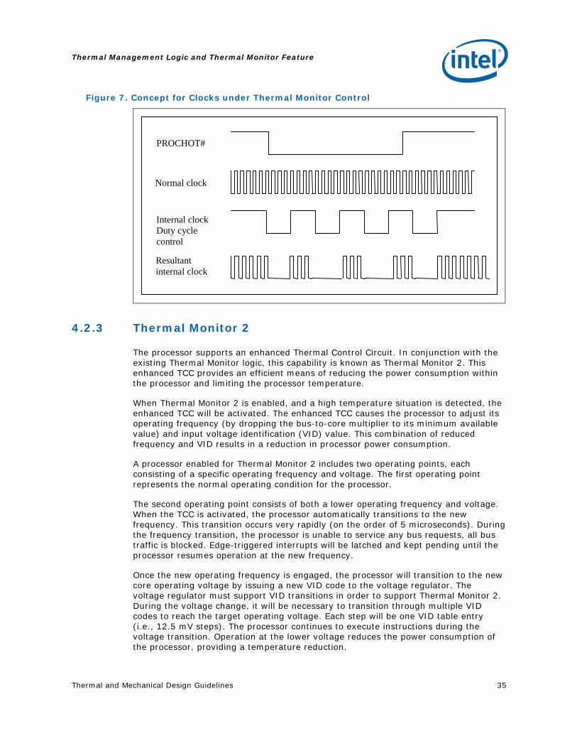
Thermal Management Logic and Thermal Monitor Feature
Thermal and Mechanical Design Guidelines 35
Figure 7. Concept for Clocks under Thermal Monitor Control
PROCHOT#
Resultantinternal clock
Normal clock
Internal clockDuty cyclecontrol
4.2.3 Thermal Monitor 2
The processor supports an enhanced Thermal Control Circuit. In conjunction with the existing Thermal Monitor logic, this capability is known as Thermal Monitor 2. This enhanced TCC provides an efficient means of reducing the power consumption within the processor and limiting the processor temperature.
When Thermal Monitor 2 is enabled, and a high temperature situation is detected, the enhanced TCC will be activated. The enhanced TCC causes the processor to adjust its operating frequency (by dropping the bus-to-core multiplier to its minimum available value) and input voltage identification (VID) value. This combination of reduced frequency and VID results in a reduction in processor power consumption.
A processor enabled for Thermal Monitor 2 includes two operating points, each consisting of a specific operating frequency and voltage. The first operating point represents the normal operating condition for the processor.
The second operating point consists of both a lower operating frequency and voltage. When the TCC is activated, the processor automatically transitions to the new frequency. This transition occurs very rapidly (on the order of 5 microseconds). During the frequency transition, the processor is unable to service any bus requests, all bus traffic is blocked. Edge-triggered interrupts will be latched and kept pending until the processor resumes operation at the new frequency.
Once the new operating frequency is engaged, the processor will transition to the new core operating voltage by issuing a new VID code to the voltage regulator. The voltage regulator must support VID transitions in order to support Thermal Monitor 2. During the voltage change, it will be necessary to transition through multiple VID codes to reach the target operating voltage. Each step will be one VID table entry (i.e., 12.5 mV steps). The processor continues to execute instructions during the voltage transition. Operation at the lower voltage reduces the power consumption of the processor, providing a temperature reduction.

Thermal Management Logic and Thermal Monitor Feature
36 Thermal and Mechanical Design Guidelines
Once the processor has sufficiently cooled, and a minimum activation time has expired, the operating frequency and voltage transition back to the normal system operating point. Transition of the VID code will occur first, in order to insure proper operation once the processor reaches its normal operating frequency. Refer to Figure 8 for an illustration of this ordering.
Figure 8. Thermal Monitor 2 Frequency and Voltage Ordering
VID
Frequency
TemperatureTTM2
fMAX
fTM2
VID
VIDTM2
PROCHOT#
Time
Refer to the datasheet for further information on Thermal Monitor 2.
4.2.4 Operation and Configuration
To maintain compatibility with previous generations of processors, which have no integrated thermal logic, the Thermal Control Circuit portion of Thermal Monitor is disabled by default. During the boot process, the BIOS must enable the Thermal Control Circuit. Thermal Monitor must be enabled to ensure proper processor operation.
The Thermal Control Circuit feature can be configured and monitored in a number of ways. OEMs are required to enable the Thermal Control Circuit while using various registers and outputs to monitor the processor thermal status. The Thermal Control Circuit is enabled by the BIOS setting a bit in an MSR (model specific register). Enabling the Thermal Control Circuit allows the processor to attempt to maintain a safe operating temperature without the need for special software drivers or interrupt handling routines. When the Thermal Control Circuit has been enabled, processor power consumption will be reduced after the thermal sensor detects a high temperature, i.e. PROCHOT# assertion. The Thermal Control Circuit and PROCHOT# transitions to inactive once the temperature has been reduced below the thermal trip point, although a small time-based hysteresis has been included to prevent multiple PROCHOT# transitions around the trip point. External hardware can monitor PROCHOT# and generate an interrupt whenever there is a transition from active-to-inactive or inactive-to-active. PROCHOT# can also be configured to generate an internal interrupt which would initiate an OEM supplied interrupt service routine.

Thermal Management Logic and Thermal Monitor Feature
Thermal and Mechanical Design Guidelines 37
Regardless of the configuration selected, PROCHOT# will always indicate the thermal status of the processor.
The power reduction mechanism of thermal monitor can also be activated manually using an “on-demand” mode. Refer to Section 4.2.5 for details on this feature.
4.2.5 On-Demand Mode
For testing purposes, the thermal control circuit may also be activated by setting bits in the ACPI MSRs. The MSRs may be set based on a particular system event (e.g., an interrupt generated after a system event), or may be set at any time through the operating system or custom driver control thus forcing the thermal control circuit on. This is referred to as “on-demand” mode. Activating the thermal control circuit may be useful for thermal solution investigations or for performance implication studies. When using the MSRs to activate the on-demand clock modulation feature, the duty cycle is configurable in steps of 12.5%, from 12.5% to 87.5%.
For any duty cycle, the maximum time period the clocks are disabled is ~3 μs. This time period is frequency dependent, and decreases as frequency increases. To achieve different duty cycles, the length of time that the clocks are disabled remains constant, and the time period that the clocks are enabled is adjusted to achieve the desired ratio. For example, if the clock disable period is 3 µs, and a duty cycle of ¼ (25%) is selected, the clock on time would be reduced to approximately 1 μs [on time (1 μs) ÷ total cycle time (3 + 1) μs = ¼ duty cycle]. Similarly, for a duty cycle of 7/8 (87.5%), the clock on time would be extended to 21 μs [21 ÷ (21 + 3) = 7/8 duty cycle].
In a high temperature situation, if the thermal control circuit and ACPI MSRs (automatic and on-demand modes) are used simultaneously, the fixed duty cycle determined by automatic mode would take precedence.
Note: On-demand mode can not activate the power reduction mechanism of Thermal Monitor 2
4.2.6 System Considerations
Intel requires the Thermal Monitor and Thermal Control Circuit to be enabled for all processors. The thermal control circuit is intended to protect against short term thermal excursions that exceed the capability of a well designed processor thermal solution. Thermal Monitor should not be relied upon to compensate for a thermal solution that does not meet the thermal profile up to the thermal design power (TDP).
Each application program has its own unique power profile, although the profile has some variability due to loop decisions, I/O activity and interrupts. In general, compute intensive applications with a high cache hit rate dissipate more processor power than applications that are I/O intensive or have low cache hit rates.
The processor TDP is based on measurements of processor power consumption while running various high power applications. This data is used to determine those applications that are interesting from a power perspective. These applications are then evaluated in a controlled thermal environment to determine their sensitivity to activation of the thermal control circuit. This data is used to derive the TDP targets published in the processor datasheet.

Thermal Management Logic and Thermal Monitor Feature
38 Thermal and Mechanical Design Guidelines
A system designed to meet the thermal profile at TDP and TC-MAX values published in the processor datasheet greatly reduces the probability of real applications causing the thermal control circuit to activate under normal operating conditions. Systems that do not meet these specifications could be subject to more frequent activation of the thermal control circuit depending upon ambient air temperature and application power profile. Moreover, if a system is significantly under designed, there is a risk that the Thermal Monitor feature will not be capable of maintaining a safe operating temperature and the processor could shutdown and signal THERMTRIP#.
For information regarding THERMTRIP#, refer to the processor datasheet and to Section 4.2.8 of this Thermal Design Guidelines.
4.2.7 Operating System and Application Software Considerations
The Thermal Monitor feature and its thermal control circuit work seamlessly with ACPI compliant operating systems. The Thermal Monitor feature is transparent to application software since the processor bus snooping, ACPI timer, and interrupts are active at all times.
4.2.8 THERMTRIP# Signal
In the event of a catastrophic cooling failure, the processor will automatically shut down when the silicon temperature has reached its operating limit. At this point the system bus signal THERMTRIP# goes active and power must be removed from the processor. THERMTRIP# activation is independent of processor activity and does not generate any bus cycles. Refer to the processor datasheet for more information about THERMTRIP#.
The temperature where the THERMTRIP# signal goes active is individually calibrated during manufacturing. The temperature where THERMTRIP# goes active is roughly parallel to the thermal profile and greater than the PROCHOT# activation temperature. Once configured, the temperature at which the THERMTRIP# signal is asserted is neither re-configurable nor accessible to the system.
4.2.9 Cooling System Failure Warning
It may be useful to use the PROCHOT# signal as an indication of cooling system failure. Messages could be sent to the system administrator to warn of the cooling failure, while the thermal control circuit would allow the system to continue functioning or allow a normal system shutdown. If no thermal management action is taken, the silicon temperature may exceed the operating limits, causing THERMTRIP# to activate and shut down the processor. Regardless of the system design requirements or thermal solution ability, the Thermal Monitor feature must still be enabled to ensure proper processor operation.
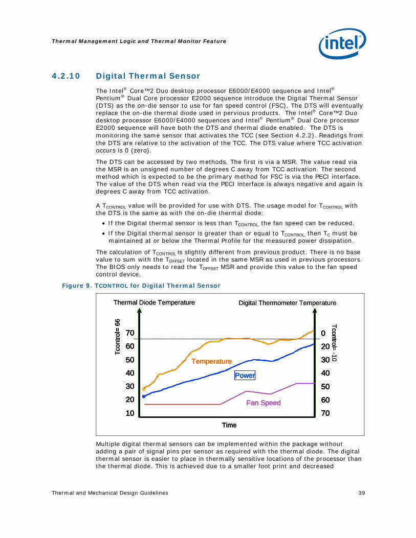
Thermal Management Logic and Thermal Monitor Feature
Thermal and Mechanical Design Guidelines 39
4.2.10 Digital Thermal Sensor
The Intel® Core™2 Duo desktop processor E6000/E4000 sequence and Intel® Pentium® Dual Core processor E2000 sequence introduce the Digital Thermal Sensor (DTS) as the on-die sensor to use for fan speed control (FSC). The DTS will eventually replace the on-die thermal diode used in pervious products. The Intel® Core™2 Duo desktop processor E6000/E4000 sequences and Intel® Pentium® Dual Core processor E2000 sequence will have both the DTS and thermal diode enabled. The DTS is monitoring the same sensor that activates the TCC (see Section 4.2.2). Readings from the DTS are relative to the activation of the TCC. The DTS value where TCC activation occurs is 0 (zero).
The DTS can be accessed by two methods. The first is via a MSR. The value read via the MSR is an unsigned number of degrees C away from TCC activation. The second method which is expected to be the primary method for FSC is via the PECI interface. The value of the DTS when read via the PECI interface is always negative and again is degrees C away from TCC activation.
A TCONTROL value will be provided for use with DTS. The usage model for TCONTROL with the DTS is the same as with the on-die thermal diode:
• If the Digital thermal sensor is less than TCONTROL, the fan speed can be reduced.
• If the Digital thermal sensor is greater than or equal to TCONTROL, then TC must be maintained at or below the Thermal Profile for the measured power dissipation.
The calculation of TCONTROL is slightly different from previous product. There is no base value to sum with the TOFFSET located in the same MSR as used in previous processors. The BIOS only needs to read the TOFFSET MSR and provide this value to the fan speed control device.
Figure 9. TCONTROL for Digital Thermal Sensor
Digital Thermometer Temperature
30
20
10
70
60
50
40
30
20
0
70
60
50
40
Tcon
trol=
66 Tcontrol= -10
Fan Speed
Temperature
Time
Power
Thermal Diode Temperature
30
20
10
70
60
50
40
30
20
10
70
60
50
40
30
20
0
70
60
50
40
30
20
0
70
60
50
40
Tcon
trol=
66 Tcontrol
Fan Speed
Temperature
Time
Power
Digital Thermometer Temperature
30
20
10
70
60
50
40
30
20
0
70
60
50
40
Tcon
trol=
66 Tcontrol= -10
Fan Speed
Temperature
Time
Power
Thermal Diode Temperature
30
20
10
70
60
50
40
30
20
10
70
60
50
40
30
20
0
70
60
50
40
30
20
0
70
60
50
40
Tcon
trol=
66 Tcontrol
Fan Speed
Temperature
Time
Power
Multiple digital thermal sensors can be implemented within the package without adding a pair of signal pins per sensor as required with the thermal diode. The digital thermal sensor is easier to place in thermally sensitive locations of the processor than the thermal diode. This is achieved due to a smaller foot print and decreased
Thermal Management Logic and Thermal Monitor Feature
40 Thermal and Mechanical Design Guidelines
sensitivity to noise. Since the DTS is factory set on a per-part basis there is no need for the health monitor components to be updated at each processor family.
Note: Intel® Core™2 Duo processor E6000 and E4000 sequences and Intel® Pentium® Dual Core processor E2000 sequence do not have an on-die thermal diode. The TCONTROL in the MSR is relevant only to the DTS.
4.2.11 Platform Environmental Control Interface (PECI)
The PECI interface is a proprietary single wire bus between the processor and the chipset or other health monitoring device. At this time the digital thermal sensor is the only data being transmitted. For an overview of the PECI interface see PECI Feature Set Overview. For additional information on the PECI see the Intel® Core™2 Duo Extreme Processor X6800 and Intel® Core™2 Duo Desktop Processor E6000 and E4000 Sequence Datasheet.
The PECI bus is available on pin G5 of the LGA 775 socket. Starting with the Intel ICH8 IO Controller Hub has integrated a PECI host controller. The PECI interface and the Manageability Engine, embedded in the Intel 965 Express chipset family, are key elements to the Intel® Quiet System Technology (Intel® QST), see Chapter 7 and the Intel® Quiet System Technology Configuration and Tuning Manual.
Intel has worked with many vendors that provide fan speed control devices to provide PECI host controllers. Consult the local representative for your preferred vendor for their product plans and availability.
§
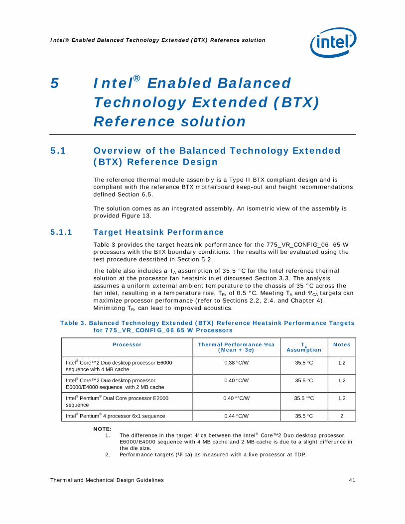
Intel® Enabled Balanced Technology Extended (BTX) Reference solution
Thermal and Mechanical Design Guidelines 41
5 Intel® Enabled Balanced Technology Extended (BTX) Reference solution
5.1 Overview of the Balanced Technology Extended (BTX) Reference Design
The reference thermal module assembly is a Type II BTX compliant design and is compliant with the reference BTX motherboard keep-out and height recommendations defined Section 6.5.
The solution comes as an integrated assembly. An isometric view of the assembly is provided Figure 13.
5.1.1 Target Heatsink Performance Table 3 provides the target heatsink performance for the 775_VR_CONFIG_06 65 W processors with the BTX boundary conditions. The results will be evaluated using the test procedure described in Section 5.2.
The table also includes a TA assumption of 35.5 °C for the Intel reference thermal solution at the processor fan heatsink inlet discussed Section 3.3. The analysis assumes a uniform external ambient temperature to the chassis of 35 °C across the fan inlet, resulting in a temperature rise, TR, of 0.5 °C. Meeting TA and ΨCA targets can maximize processor performance (refer to Sections 2.2, 2.4. and Chapter 4). Minimizing TR, can lead to improved acoustics.
Table 3. Balanced Technology Extended (BTX) Reference Heatsink Performance Targets for 775_VR_CONFIG_06 65 W Processors
Processor Thermal Performance Ψca (Mean + 3σ)
TA Assumption
Notes
Intel® Core™2 Duo desktop processor E6000 sequence with 4 MB cache
0.38 °C/W 35.5 °C 1,2
Intel® Core™2 Duo desktop processor E6000/E4000 sequence with 2 MB cache
0.40 °C/W 35.5 °C 1,2
Intel® Pentium® Dual Core processor E2000 sequence
0.40 °°C/W 35.5 °°C 1,2
Intel® Pentium® 4 processor 6x1 sequence 0.44 °C/W 35.5 °C 2
NOTE: 1. The difference in the target Ψ ca between the Intel® Core™2 Duo desktop processor
E6000/E4000 sequence with 4 MB cache and 2 MB cache is due to a slight difference in the die size.
2. Performance targets (Ψ ca) as measured with a live processor at TDP.

Intel® Enabled Balanced Technology Extended (BTX) Reference solution
42 Thermal and Mechanical Design Guidelines
5.1.2 Acoustics
To optimize acoustic emission by the fan heatsink assembly, the reference design implements a variable speed fan. A variable speed fan allows higher thermal performance at higher fan inlet temperatures (TA) and the appropriate thermal performance with improved acoustics at lower fan inlet temperatures. The required fan speed necessary to meet thermal specifications can be controlled by the fan inlet temperature and should comply with requirements below:
Table 4. Acoustic Targets
Fan Speed RPM
Thermistor Set Point
Acoustic Thermal Performance Ψca Notes
~ 5300 High TA ≥ 35 °C
≤ 6.4 BA • 0.38 °C/W (Intel® Core™2 Duo processors - 4 MB)
• 0.40 °C/W (Intel® Core™2 Duo processors - 2 MB)
• 0.40 °C/W (Intel® Pentium Dual-Core E2000 sequence)
• 0.44 °C/W (Intel® Pentium® 4 processor 6x1 sequence)
Case 1: Thermal Design Power Maximum fan speed 100% PWM duty cycle
~ 2500 Low TA = 23 °C
No Target Defined
• 0.56 °C/W (Intel® Core™2 Duo processors - 4 MB)
• 0.58 °C/W (Intel® Core™2 Duo processors - 2 MB)
• 0.58 °C/W (Intel® Pentium Dual-Core E2000 sequence)
• 0.63 °C/W (Intel® Pentium® 4 processor 6x1 sequence)
Case 2 Thermal Design Power System (PSU, HDD, TMA) Fan speed limited by the fan hub thermistor
~ 1400 Low TA = 23 °C
≤ 3.4 BA • ~0.87 °C/W (Intel® Core™2 Duo processors - 4 MB)
• ~0.89 °C/W (Intel® Core™2 Duo processors - 2 MB)
• ~0.89 °C/W (Intel® Pentium Dual-Core E2000 sequence)
• ~0.93 °C/W (Intel® Pentium® 4 processor 6x1 sequence)
Case 3 50% Thermal Design Power TMA Only
~ 1400 Low TA = 23 °C
≤ 4.0 BA • ~0.87 °C/W (Intel® Core™2 Duo processors - 4 MB)
• ~0.89 °C/W (Intel® Core™2 Duo processors - 2 MB)
• ~0.89 °C/W (Intel® Pentium Dual-Core E2000 sequence)
• ~0.93 °C/W (Intel® Pentium® 4 processor 6x1 sequence)
Case 3 50% Thermal Design Power System (PSU, HDD, TMA)
NOTE: 1. Acoustic performance is defined in terms of measured sound power (LwA) as defined in
ISO 9296 standard, and measured according to ISO 7779. 2. Acoustic testing will be for the TMA only when installed in a BTX S2 chassis for Case 1
and 3

Intel® Enabled Balanced Technology Extended (BTX) Reference solution
Thermal and Mechanical Design Guidelines 43
3. Acoustics testing for Case 2 will be system level in the same a BTX S2 reference chassis and commercially available power supply. Acoustic data for Case 2 will be provided in the validation report but this condition is not a target for the design. The acoustic model is predicting that the power supply fan will be the acoustic limiter.
4. The fan speeds (RPM) are estimates for one of the two reference fans and will be adjusted to meet thermal performance targets then acoustic target during validation. The designer should identify the fan speed required to meet the effective fan curve shown in Section 5.1.3
5. Minimum fan speed is expected to be no higher than 1200 RPM for the fan being used in validation testing.
While the fan hub thermistor helps optimize acoustics at high processor workloads by adapting the maximum fan speed to support the processor thermal profile, additional acoustic improvements can be achieved at lower processor workload by using the TCONTROL specifications described in Section 2.2.3. Intel’s recommendation is to use the Fan Specification for 4 Wire PWM Controlled Fans to implement fan speed control capability based the digital thermal sensor. Refer to Chapter 7 for further details.
5.1.3 Effective Fan Curve
The TMA must fulfill the processor cooling requirements shown in Table 3 when it is installed in a functional BTX system. When installed in a system, the TMA must operate against the backpressure created by the chassis impedance (due to vents, bezel, peripherals, etc…) and will operate at lower net airflow than if it were tested outside of the system on a bench top or open air environment. Therefore an allowance must be made to accommodate or predict the reduction in Thermal Module performance due to the reduction in heatsink airflow from chassis impedance. For this reason, it is required that the Thermal Module satisfy the prescribed ΨCA requirements when operating against an impedance that is characteristic for BTX platforms.
Because of the coupling between TMA thermal performance and system impedance, the designer should understand the TMA effective fan curve. This effective fan curve represents the performance of the fan component AND the impedance of the stator, heatsink, duct, and flow partitioning devices. The BTX system integrator will be able to evaluate a TMA based on the effective fan curve of the assembly and the airflow impedance of their target system.
Note: It is likely that at some operating points the fans speed will be driven by the system airflow requirements and not the processor thermal limits.
Figure 10 shows the effective fan curve for the reference design TMA. These curves are based on analysis. The boundary conditions used are the S2 6.9L reference chassis, the reference TMA with the flow portioning device, extrusion and an AVC Type II fan geometry.
When selecting a fan for use in the TMA care should be taken that similar effective fan curves can be achieved. Final verification requires the overlay of the Type II MASI curve to ensure thermal compliance.
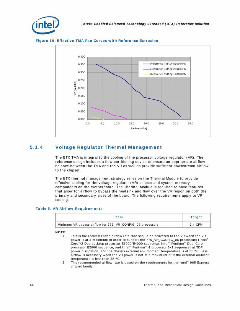
Intel® Enabled Balanced Technology Extended (BTX) Reference solution
44 Thermal and Mechanical Design Guidelines
Figure 10. Effective TMA Fan Curves with Reference Extrusion
0.000
0.050
0.100
0.150
0.200
0.250
0.300
0.350
0.400
0.0 5.0 10.0 15.0 20.0 25.0 30.0 35.0
Airflow (cfm)
dP (i
n. H
2O)
Reference TMA @ 5300 RPM
Reference TMA @ 2500 RPM
Reference TMA @ 1200 RPM
5.1.4 Voltage Regulator Thermal Management
The BTX TMA is integral to the cooling of the processor voltage regulator (VR). The reference design includes a flow partitioning device to ensure an appropriate airflow balance between the TMA and the VR as well as provide sufficient downstream airflow to the chipset.
The BTX thermal management strategy relies on the Thermal Module to provide effective cooling for the voltage regulator (VR) chipset and system memory components on the motherboard. The Thermal Module is required to have features that allow for airflow to bypass the heatsink and flow over the VR region on both the primary and secondary sides of the board. The following requirements apply to VR cooling.
Table 5. VR Airflow Requirements
Item Target
Minimum VR bypass airflow for 775_VR_CONFIG_06 processors 2.4 CFM
NOTE: 1. This is the recommended airflow rate that should be delivered to the VR when the VR
power is at a maximum in order to support the 775_VR_CONFIG_06 processors (Intel® Core™2 Duo desktop processor E6000/E4000 sequence, Intel® Pentium® Dual Core processor E2000 sequence, and Intel® Pentium® 4 processor 6x1 sequence) at TDP power dissipation, and the chassis external environment temperature is at 35 ºC. Less airflow is necessary when the VR power is not at a maximum or if the external ambient temperature is less than 35 ºC.
2. This recommended airflow rate is based on the requirements for the Intel® 965 Express chipset family.

Intel® Enabled Balanced Technology Extended (BTX) Reference solution
Thermal and Mechanical Design Guidelines 45
5.1.5 Altitude
The reference TMA was evaluated at sea level. However, many companies design products that must function reliably at high altitude, typically 1,500 m [5,000 ft] or more. Air-cooled temperature calculations and measurements at sea level must be adjusted to take into account altitude effects like variation in air density and overall heat capacity. This often leads to some degradation in thermal solution performance compared to what is obtained at sea level, with lower fan performance and higher surface temperatures. The system designer needs to account for altitude effects in the overall system thermal design to make sure that the TC requirement for the processor is met at the targeted altitude.
5.1.6 Reference Heatsink Thermal Validation
The Intel reference heatsink was validated within the specific boundary conditions based on the methodology described in Section 5.2 , and using a thermal test vehicle.
Testing is done in a BTX chassis at ambient lab temperature. The test results, for a number of samples, is reported in terms of a worst-case mean + 3σ value for thermal characterization parameter using real processors (based on the thermal test vehicle correction factors).
5.1.7 Fan Performance for Active Heatsink Thermal Solution
The fan power requirements for proper operation are given Table 6.
Table 6. Fan Electrical Performance Requirements
Requirement Value
Maximum Average fan current draw 1.5 A
Fan start-up current draw 2.2 A
Fan start-up current draw maximum duration 1.0 second
Fan header voltage 12 V ±5%
Tachometer output 2 pulse per revolution
In addition to comply with overall thermal requirements (Section 6.1.1), and the general environmental reliability requirements (Section 6.2) the fan should meet the following performance requirements:
• Mechanical wear out represents the highest risk reliability parameter for fans. The capability of the functional mechanical elements (ball bearing, shaft, and tower assembly) must be demonstrated to a minimum useful lifetime of 40,000 hours.
• In addition to passing the environmental reliability tests described in Section 6.2, the fan must demonstrate adequate performance after 7,500 on/off cycles with each cycle specified as 3 minutes on, 2 minutes off, at a temperature of 70 °C.
See the Fan Specification for 4-wire PWM Controlled Fans for additional details on the fan specification.

Intel® Enabled Balanced Technology Extended (BTX) Reference solution
46 Thermal and Mechanical Design Guidelines
5.2 Environmental Reliability Testing
5.2.1 Structural Reliability Testing
Structural reliability tests consist of unpackaged, system -level vibration and shock tests of a given thermal solution in the assembled state. The thermal solution should meet the specified thermal performance targets after these tests are conducted; however, the test conditions outlined here may differ from your own system requirements.
5.2.1.1 Random Vibration Test Procedure
Recommended performance requirement for a system:
• Duration: 10 min/axis, 3 axes • Frequency Range: 5 Hz to 500 Hz
5 Hz @ .001 g2/Hz to 20 Hz @ 0.01 g2/Hz (slope up) 20 Hz to 500 Hz @ 0.01 g2/Hz (flat)
• Power Spectral Density (PSD) Profile: 2.2 G RMS
Figure 11. Random Vibration PSD
Vibration System Level
0.0001
0.001
0.01
0.1
1 10 100 1000Hz
g2 /Hz
+ 3 dB Control Limit
- 3 dB Control Limit
5.2.1.2 Shock Test Procedure
Recommended performance requirement for a system:
• Quantity: 2 drops for + and - directions in each of 3 perpendicular axes (i.e., total 12 drops).
• Profile: 25 G trapezoidal waveform 225 in/sec minimum velocity change. (systems > 20 lbm) 250 in/sec minimum velocity change. (systems < 20 lbm)
• Setup: Mount sample system on tester.

Intel® Enabled Balanced Technology Extended (BTX) Reference solution
Thermal and Mechanical Design Guidelines 47
Figure 12. Shock Acceleration Curve
5.2.1.2.1 Recommended Test Sequence
Each test sequence should start with components (i.e. motherboard, heatsink assembly, etc.) that have never been previously submitted to any reliability testing.
The test sequence should always start with a visual inspection after assembly, and BIOS/CPU/Memory test (refer to Section 6.2.3).
Prior to the mechanical shock & vibration test, the units under test should be preconditioned for 72 hours at 45 ºC. The purpose is to account for load relaxation during burn-in stage.
The stress test should be followed by a visual inspection and then BIOS/CPU/Memory test.
5.2.1.2.2 Post-Test Pass Criteria
The post-test pass criteria are:
1. No significant physical damage to the heatsink attach mechanism (including such items as clip and motherboard fasteners).
2. Heatsink must remain attached to the motherboard.
3. Heatsink remains seated and its bottom remains mated flatly against IHS surface. No visible gap between the heatsink base and processor IHS. No visible tilt of the heatsink with respect to its attach mechanism.
4. No signs of physical damage on motherboard surface due to impact of heatsink or heatsink attach mechanism.
5. No visible physical damage to the processor package.
6. Successful BIOS/Processor/memory test of post-test samples.
7. Thermal compliance testing to demonstrate that the case temperature specification can be met.

Intel® Enabled Balanced Technology Extended (BTX) Reference solution
48 Thermal and Mechanical Design Guidelines
5.2.2 Power Cycling
Thermal performance degradation due to TIM degradation is evaluated using power cycling testing. The test is defined by 7500 cycles for the case temperature from room temperature (~23 ºC) to the maximum case temperature defined by the thermal profile at TDP. Thermal Test Vehicle is used for this test.
5.2.3 Recommended BIOS/Processor/Memory Test Procedures
This test is to ensure proper operation of the product before and after environmental stresses, with the thermal mechanical enabling components assembled. The test shall be conducted on a fully operational motherboard that has not been exposed to any battery of tests prior to the test being considered.
Testing setup should include the following components, properly assembled and/or connected:
• Appropriate system motherboard
• Processor
• All enabling components, including socket and thermal solution parts
• Power supply
• Disk drive
• Video card
• DIMM
• Keyboard
• Monitor
The pass criterion is that the system under test shall successfully complete the checking of BIOS, basic processor functions and memory, without any errors.
5.3 Material and Recycling Requirements
Material shall be resistant to fungal growth. Examples of non-resistant materials include cellulose materials, animal and vegetable based adhesives, grease, oils, and many hydrocarbons. Synthetic materials such as PVC formulations, certain polyurethane compositions (e.g., polyester and some polyethers), plastics which contain organic fillers of laminating materials, paints, and varnishes also are susceptible to fungal growth. If materials are not fungal growth resistant, then MIL-STD-810E, Method 508.4 must be performed to determine material performance.
Material used shall not have deformation or degradation in a temperature life test.
Any plastic component exceeding 25 grams must be recyclable per the European Blue Angel recycling standards.

Intel® Enabled Balanced Technology Extended (BTX) Reference solution
Thermal and Mechanical Design Guidelines 49
5.4 Safety Requirements
Heatsink and attachment assemblies shall be consistent with the manufacture of units that meet the safety standards:
• UL Recognition-approved for flammability at the system level. All mechanical and thermal enabling components must be a minimum UL94V-2 approved.
• CSA Certification. All mechanical and thermal enabling components must have CSA certification.
• All components (in particular the heatsink fins) must meet the test requirements of UL1439 for sharp edges.
• If the International Accessibility Probe specified in IEC 950 can access the moving parts of the fan, consider adding safety feature so that there is no risk of personal injury.
5.5 Geometric Envelope for Intel® Reference Balanced Technology Extended (BTX) Thermal Module Assembly
Figure 73 through Figure 77 in Appendix G gives the motherboard keep-out information for the BTX thermal mechanical solutions. Additional information on BTX design considerations can be found in Balanced Technology Extended (BTX) System Design Guide available at http://www.formfactors.org.
The maximum height of the TMA above the motherboard is 60.60 mm [2.386 inches], for compliance with the motherboard primary side height constraints defined in the BTX Interface Specification for Zone A, found at http://www.formfactors.org.
Figure 13. Intel Type II TMA 65W Reference Design
Development vendor information for the Intel Type II TMA Reference Solution is provided in Appendix H.

Intel® Enabled Balanced Technology Extended (BTX) Reference solution
50 Thermal and Mechanical Design Guidelines
5.6 Preload and TMA Stiffness
5.6.1 Structural Design Strategy
Structural design strategy for the Intel Type II TMA is to minimize upward board deflection during shock to help protect the LGA775 socket.
BTX thermal solutions utilize the SRM and TMA that together resists local board curvature under the socket and minimize, board deflection (Figure 14). In addition, a moderate preload provides initial downward deflection.
Figure 14. Upward Board Deflection During Shock
5.6.2 TMA Preload vs. Stiffness
The Thermal Module assembly is required to provide a static preload to ensure protection against fatigue failure of socket solder joint. The allowable preload range for BTX platforms is provided in Table 7, but the specific target value is a function of the Thermal Module effective stiffness.
The solution space for the Thermal Module effective stiffness and applied preload combinations is shown by the shaded region of Figure 15. This solution space shows that the Thermal Module assembly must have an effective stiffness that is sufficiently large such that the minimum preload determined from the relationship requirement in Figure 15 does not exceed the maximum allowed preload shown in Table 7. Furthermore, if the Thermal Module effective stiffness is so large that the minimum preload determined from Figure 15 is below the minimum required value given in Table 7, then the Thermal Module should be re-designed to have a preload that lies within the range given in Table 7, allowing for preload tolerances.
Less curvature in region between SRM and TMA
Shock Load

Intel® Enabled Balanced Technology Extended (BTX) Reference solution
Thermal and Mechanical Design Guidelines 51
Table 7. Processor Preload Limits
Parameter Minimum Required Maximum Allowed
Notes
Processor Preload 98 N [22 lbf] 222 N [50 lbf] 1
NOTE: 1. These values represent upper and lower bounds for the processor preload. The nominal
preload design point for the Thermal Module is based on a combination of requirements of the TIM, ease of assembly and the Thermal Module effective stiffness.
Figure 15. Minimum Required Processor Preload to Thermal Module Assembly Stiffness
NOTE: 1. The shaded region shown is the acceptable domain for Thermal Module assembly
effective stiffness and processor preload combinations. The Thermal Module design should have a design preload and stiffness that lies within this region. The design tolerance for the preload and TMA stiffness should also reside within this boundary. Note that the lower and upper horizontal boundaries represent the preload limits provided in Table 7. The equation for the left hand boundary is described in note 2.
2. The equation for this section of the preload-Thermal Module stiffness boundary is given by the following relationship: Min Preload = 1.38E-3*k^2 – 1.18486k + 320.24753 for k < 300 N/mm where k is the Thermal Module assembly effective stiffness. Note that this equation is only valid in the stiffness domain of 93N/mm < k < 282N/mm. This equation would not apply, for example, for TMA stiffness less than 93N/mm.
3. The target stiffness for the 65 W Type II TMA reference design is 484 N/mm (2764 lb / in).
Note: These preload and stiffness recommendations are specific to the TMA mounting scheme that meets the BTX Interface Specification and Support Retention Mechanism (SRM) Design Guide. For TMA mounting schemes that use only the motherboard mounting hole position for TMA attach, the required preload is approximately 10–15N greater than the values stipulated in Figure 15; however, Intel has not conducted any validation testing with this TMA mounting scheme.

Intel® Enabled Balanced Technology Extended (BTX) Reference solution
52 Thermal and Mechanical Design Guidelines
Figure 16. Thermal Module Attach Pointes and Duct-to-SRM Interface Features
SRM
Front attach pointuse 6x32 screwSee detail A
Detail A
See detail B
Detail B
Rear attach pointuse 6x32 screw
Chassis PEM nut
Duct front interfacefeature see note 2
SRM
Front attach pointuse 6x32 screwSee detail A
Detail A
See detail B
Detail B
Rear attach pointuse 6x32 screw
Chassis PEM nut
Duct front interfacefeature see note 2
NOTE: 1. For clarity the motherboard is not shown in this figure. In an actual assembly, the
captive 6x32 screws in the thermal module pass through the rear holes in the motherboard designated in the socket keep-in Figure 73 through Figure 77 in Appendix G and screw into the SRM and chassis PEM features.
2. This front duct ramp feature has both outer and inner lead-in that allows the feature to slide easily into the SRM slot and around the chassis PEM nut. Note that the front PEM nut is part of the chassis not the SRM.
§
ATX Thermal/Mechanical Design Information
Thermal and Mechanical Design Guidelines 53
6 ATX Thermal/Mechanical Design Information
6.1 ATX Reference Design Requirements
Intel is not developing an ATX reference thermal solution for the Intel® Core™2 Duo desktop processor E6000/E4000 sequence, Intel® Pentium® Dual Core processor E2000 sequence, and Intel® Pentium® 4 processor 6x1 sequence with a TDP of 65 W. This chapter will document the requirements for an active air-cooled design, with a fan installed at the top of the heatsink. The thermal technology required for the 775_VR_CONFIG_06 processor is roughly equivalent to RCBFH-3, see Intel® Pentium® 4 Processor on 90 nm Process in the 775–Land LGA Package Thermal and Mechanical Design Guidelines for a complete description of this reference design
Note: Intel ATX reference design RCBFH-3 is the higher thermal solution performance of the 65 W 775_VR_CONFIG_06 requirements (It requires ΨCA. of 0.04 °C/W lower than the 65 W 775_VR_CONFIG_06 requirements). It generates an improvement in acoustic performance to reduce the fan speed to show the acoustic advantage (acoustic results are in Table 9).
Note: If the heatsink design is used in your product for cost savings instead of acoustic advantage, the design that optimizes cost would likely use aluminum core type designs with the similar fan or a combination of all these (the smaller copper core, the less expensive fan, and the lower fin density extrusion).
The ATX motherboard keep-out and height recommendations defined Section 6.5 remain the same for a thermal solution for the Intel® Core™2 Duo desktop processor E6000/E4000 sequence and Intel® Pentium® Dual Core processor E2000 sequence with a TDP of 65 W. The solution should come as an integrated assembly. An example of an exploded view of the assembly is provided Figure 19.
Note: The 65 W 775_VR_CONFIG_06 mechanical requirements would need to meet all the published mechanical requirements for 2005 Performance 775_VR_CONFIG_05 solutions (RCFH-4); such as, the mechanical keep-in, keep-out, symmetry and socket loading.
Note: If this fan design is used in your product and you will deliver it to end use customers, you have the responsibility to determine an adequate level of protection (e.g., protection barriers, a cage, or an interlock) against contact with the energized fan by the user during user servicing.
6.1.1 Target Heatsink Performance Table 8 provides the target heatsink performance for the 775_VR_CONFIG_06 65 W processors with ATX boundary conditions. The results are based on the test procedure described in Section 6.1.4.
The table also includes a TA assumption of 40 °C for the Intel reference thermal solution at the processor fan heatsink inlet discussed Section 3.3. An external ambient temperature to the chassis of 35 °C is assumed, resulting in a temperature rise, TR, of 5 °C. Meeting TA and ΨCA targets can maximize processor performance (refer to Sections 2.2, 2.4. and Chapter 4). Minimizing TR can lead to improved acoustics.

ATX Thermal/Mechanical Design Information
54 Thermal and Mechanical Design Guidelines
Table 8. ATX Target Heatsink Performance in 775_VR_CONFIG_06 65 W Processor
Processor Thermal Performance Ψca (Mean + 3σ)
TA Assumption
Notes
Intel® Core™2 Duo desktop processor E6000 sequence with 4 MB cache
0.31 °C/W 40 °C 1, 2
Intel® Core™2 Duo desktop processor E6000/E4000 sequence with 2 MB cache
0.33 °C/W 40 °C 1, 2
Intel® Pentium® Dual Core processor E2000 sequence
0.33 °C/W 40 °C 2
Intel® Pentium® 4 processor 6x1 sequence 0.37 °C/W 40 °C 2
NOTE: 1. The difference in Ψ ca between the Intel® Core™2 Duo desktop processor E6000/E4000
sequence with 4 MB cache and 2 MB cache is due to a slight difference in the die size. 2. Performance targets (Ψ ca) as measured with a live processor at TDP.
6.1.2 Acoustics
To optimize acoustic emission by the fan heatsink assembly, Intel recommends the use of a thermistor controlled variable speed fan. A variable speed fan allows higher thermal performance at higher fan inlet temperatures (TA) and lower thermal performance with improved acoustics at lower fan inlet temperatures. The required fan speed necessary to meet thermal specifications can be controlled by the fan inlet temperature and should comply with requirements below:
Table 9. Acoustic Results
Fan Speed RPM
Thermistor Set Point
Acoustic Thermal Performance Ψca Notes
2300 High TA = 40 °C
4.1 BA 0.31 °C/W (Intel® Core™2 Duo Processor - 4 MB)
0.33 °C/W (Intel® Core™2 Duo Processor - 2 MB)
0.33 °C/W (Intel® Pentium Dual-Core E2000 sequence)
0.37 °C/W (Intel® Pentium® 6x1 sequence)
1000 Low TA = 28 °C
3.3 BA 0.49 °C/W (Intel® Core™2 Duo Processor - 4 MB)
0.51 °C/W (Intel® Core™2 Duo Processor - 2 MB)
0.51 °C/W (Intel® Pentium Dual-Core E2000 sequence)
0.56 °C/W (Intel® Pentium® 6x1 sequence)
Thermal Design Power, Fan speed limited by the fan hub thermistor
1000 Low TA = 28 °C
3.3 BA Minimum fan speed
Note: Acoustic performance is defined in terms of measured sound power (LwA) as defined in ISO 9296 standard, and measured according to ISO 7779.

ATX Thermal/Mechanical Design Information
Thermal and Mechanical Design Guidelines 55
While the fan hub thermistor helps optimize acoustics at high processor workloads by adapting the maximum fan speed to support the processor thermal profile, additional acoustic improvements can be achieved at lower processor workload by using the TCONTROL specifications described in Section 2.2.3. Intel recommendation is to use the Fan Specification for 4 Wire PWM Controlled Fans to implement fan speed control capability based digital thermal sensor temperature. Refer to Chapter 7 for further details.
6.1.3 Altitude
Many companies design products that must function reliably at high altitude, typically 1,500 m [5,000 ft] or more. Air-cooled temperature calculations and measurements at the test site elevation must be adjusted to take into account altitude effects like variation in air density and overall heat capacity. This often leads to some degradation in thermal solution performance compared to what is obtained at sea level, with lower fan performance and higher surface temperatures. The system designer needs to account for altitude effects in the overall system thermal design to make sure that the TC requirement for the processor is met at the targeted altitude.
6.1.4 Heatsink Thermal Validation
Intel recommends evaluation of the heatsink within the specific boundary conditions based on the methodology described Section 6.2 , and using a thermal test vehicle.
Testing is done on bench top test boards at ambient lab temperature. In particular, for the reference heatsink, the Plexiglas* barrier is installed 81.28 mm [3.2 in] above the motherboard (refer to Sections 3.3 and 6.5).
The test results, for a number of samples, are reported in terms of a worst-case mean + 3σ value for thermal characterization parameter using real processors (based on the thermal test vehicle correction factors).
Note: The above 81.28 mm obstruction height that is used for testing complies with the recommended obstruction height of 88.9 mm for the ATX form factor. However, it would conflict with systems in strict compliance with the ATX specification which allows an obstruction as low as 76.2 mm above the motherboard surface in Area A.
6.1.5 Fan Performance for Active Heatsink Thermal Solution
The fan power requirements for proper operation are given Table 10.
Table 10. Fan Electrical Performance Requirements
Requirement Value
Maximum Average fan current draw 1.5 A
Fan start-up current draw 2.2 A
Fan start-up current draw maximum duration 1.0 second
Fan header voltage 12 V ±5%
Tachometer output 2 pulse per revolution

ATX Thermal/Mechanical Design Information
56 Thermal and Mechanical Design Guidelines
In addition to comply with overall thermal requirements (Section 6.1.1), and the general environmental reliability requirements (Section 6.2) the fan should meet the following performance requirements:
• Mechanical wear out represents the highest risk reliability parameter for fans. The capability of the functional mechanical elements (ball bearing, shaft, and tower assembly) must be demonstrated to a minimum useful lifetime of 50,000 hours.
• In addition to passing the environmental reliability tests described in Section 6.2, the fan must demonstrate adequate performance after 7,500 on/off cycles with each cycle specified as 3 minutes on, 2 minutes off, at a temperature of 70 °C.
See the Fan Specification for 4-wire PWM Controlled Fans for additional details on the fan specification.
6.2 Environmental Reliability Testing
6.2.1 Structural Reliability Testing
Structural reliability tests consist of unpackaged, board-level vibration and shock tests of a given thermal solution in the assembled state. The thermal solution should meet the specified thermal performance targets after these tests are conducted; however, the test conditions outlined here may differ from your own system requirements.
6.2.1.1 Random Vibration Test Procedure
Duration: 10 min/axis, 3 axes
Frequency Range: 5 Hz to 500 Hz
Power Spectral Density (PSD) Profile: 3.13 G RMS

ATX Thermal/Mechanical Design Information
Thermal and Mechanical Design Guidelines 57
Figure 17. Random Vibration PSD
0.001
0.01
0.1
1 10 100 1000 Frequency (Hz)
PSD
(g^2
/Hz)
3.13GRMS (10 minutes per axis)
5 Hz 500 Hz
(5, 0.01)
(20, 0.02) (500, 0.02)
6.2.1.2 Shock Test Procedure
Recommended performance requirement for a motherboard:
• Quantity: 3 drops for + and - directions in each of 3 perpendicular axes (i.e., total 18 drops).
• Profile: 50 G trapezoidal waveform, 170 in/sec minimum velocity change.
• Setup: Mount sample board on test fixture.
Figure 18. Shock Acceleration Curve
0
10
20
30
40
50
60
0 2 4 6 8 10 12 Time (milliseconds)
A c c e l e r a t i o n
(g)

ATX Thermal/Mechanical Design Information
58 Thermal and Mechanical Design Guidelines
6.2.1.2.1 Recommended Test Sequence
Each test sequence should start with components (i.e., motherboard, heatsink assembly, etc.) that have never been previously submitted to any reliability testing.
The test sequence should always start with a visual inspection after assembly, and BIOS/processor/Memory test (refer to Section 6.2.3).
Prior to the mechanical shock & vibration test, the units under test should be preconditioned for 72 hours at 45 ºC. The purpose is to account for load relaxation during burn-in stage.
The stress test should be followed by a visual inspection and then BIOS/processor/Memory test.
6.2.1.2.2 Post-Test Pass Criteria
The post-test pass criteria are:
1. No significant physical damage to the heatsink attach mechanism (including such items as clip and motherboard fasteners).
2. Heatsink must remain attached to the motherboard.
3. Heatsink remains seated and its bottom remains mated flatly against IHS surface. No visible gap between the heatsink base and processor IHS. No visible tilt of the heatsink with respect to its attach mechanism.
4. No signs of physical damage on motherboard surface due to impact of heatsink or heatsink attach mechanism.
5. No visible physical damage to the processor package.
6. Successful BIOS/Processor/memory test of post-test samples.
7. Thermal compliance testing to demonstrate that the case temperature specification can be met.
6.2.2 Power Cycling
Thermal performance degradation due to TIM degradation is evaluated using power cycling testing. The test is defined by 7500 cycles for the case temperature from room temperature (~23 ºC) to the maximum case temperature defined by the thermal profile at TDP. A thermal test vehicle is used for this test.

ATX Thermal/Mechanical Design Information
Thermal and Mechanical Design Guidelines 59
6.2.3 Recommended BIOS/Processor/Memory Test Procedures
This test is to ensure proper operation of the product before and after environmental stresses, with the thermal mechanical enabling components assembled. The test shall be conducted on a fully operational motherboard that has not been exposed to any battery of tests prior to the test being considered.
Testing setup should include the following components, properly assembled and/or connected:
• Appropriate system motherboard
• Processor
• All enabling components, including socket and thermal solution parts
• Power supply
• Disk drive
• Video card
• DIMM
• Keyboard
• Monitor
The pass criterion is that the system under test shall successfully complete the checking of BIOS, basic processor functions and memory, without any errors.
6.3 Material and Recycling Requirements
Material shall be resistant to fungal growth. Examples of non-resistant materials include cellulose materials, animal and vegetable based adhesives, grease, oils, and many hydrocarbons. Synthetic materials such as PVC formulations, certain polyurethane compositions (e.g., polyester and some polyethers), plastics which contain organic fillers of laminating materials, paints, and varnishes also are susceptible to fungal growth. If materials are not fungal growth resistant, then MIL-STD-810E, Method 508.4 must be performed to determine material performance.
Material used shall not have deformation or degradation in a temperature life test.
Any plastic component exceeding 25 grams must be recyclable per the European Blue Angel recycling standards.
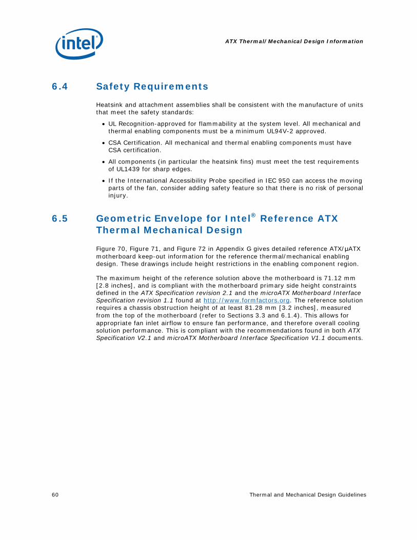
ATX Thermal/Mechanical Design Information
60 Thermal and Mechanical Design Guidelines
6.4 Safety Requirements
Heatsink and attachment assemblies shall be consistent with the manufacture of units that meet the safety standards:
• UL Recognition-approved for flammability at the system level. All mechanical and thermal enabling components must be a minimum UL94V-2 approved.
• CSA Certification. All mechanical and thermal enabling components must have CSA certification.
• All components (in particular the heatsink fins) must meet the test requirements of UL1439 for sharp edges.
• If the International Accessibility Probe specified in IEC 950 can access the moving parts of the fan, consider adding safety feature so that there is no risk of personal injury.
6.5 Geometric Envelope for Intel® Reference ATX Thermal Mechanical Design
Figure 70, Figure 71, and Figure 72 in Appendix G gives detailed reference ATX/μATX motherboard keep-out information for the reference thermal/mechanical enabling design. These drawings include height restrictions in the enabling component region.
The maximum height of the reference solution above the motherboard is 71.12 mm [2.8 inches], and is compliant with the motherboard primary side height constraints defined in the ATX Specification revision 2.1 and the microATX Motherboard Interface Specification revision 1.1 found at http://www.formfactors.org. The reference solution requires a chassis obstruction height of at least 81.28 mm [3.2 inches], measured from the top of the motherboard (refer to Sections 3.3 and 6.1.4). This allows for appropriate fan inlet airflow to ensure fan performance, and therefore overall cooling solution performance. This is compliant with the recommendations found in both ATX Specification V2.1 and microATX Motherboard Interface Specification V1.1 documents.
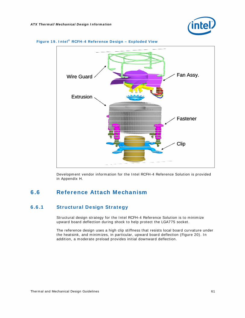
ATX Thermal/Mechanical Design Information
Thermal and Mechanical Design Guidelines 61
Figure 19. Intel® RCFH-4 Reference Design – Exploded View
Wire Guard Fan Assy.
Extrusion
Clip
Fastener
Wire Guard Fan Assy.
Extrusion
Clip
Fastener
Development vendor information for the Intel RCFH-4 Reference Solution is provided in Appendix H.
6.6 Reference Attach Mechanism
6.6.1 Structural Design Strategy
Structural design strategy for the Intel RCFH-4 Reference Solution is to minimize upward board deflection during shock to help protect the LGA775 socket.
The reference design uses a high clip stiffness that resists local board curvature under the heatsink, and minimizes, in particular, upward board deflection (Figure 20). In addition, a moderate preload provides initial downward deflection.
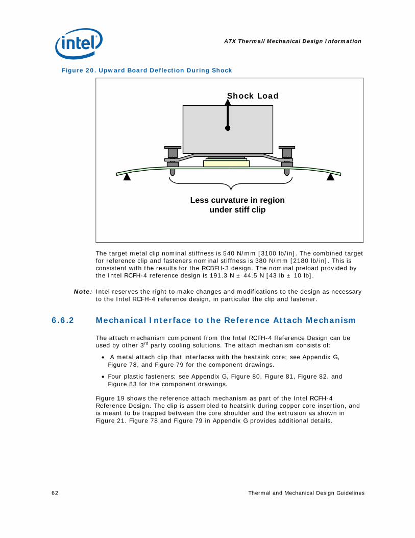
ATX Thermal/Mechanical Design Information
62 Thermal and Mechanical Design Guidelines
Figure 20. Upward Board Deflection During Shock
The target metal clip nominal stiffness is 540 N/mm [3100 lb/in]. The combined target for reference clip and fasteners nominal stiffness is 380 N/mm [2180 lb/in]. This is consistent with the results for the RCBFH-3 design. The nominal preload provided by the Intel RCFH-4 reference design is 191.3 N ± 44.5 N [43 lb ± 10 lb].
Note: Intel reserves the right to make changes and modifications to the design as necessary to the Intel RCFH-4 reference design, in particular the clip and fastener.
6.6.2 Mechanical Interface to the Reference Attach Mechanism
The attach mechanism component from the Intel RCFH-4 Reference Design can be used by other 3rd party cooling solutions. The attach mechanism consists of:
• A metal attach clip that interfaces with the heatsink core; see Appendix G, Figure 78, and Figure 79 for the component drawings.
• Four plastic fasteners; see Appendix G, Figure 80, Figure 81, Figure 82, and Figure 83 for the component drawings.
Figure 19 shows the reference attach mechanism as part of the Intel RCFH-4 Reference Design. The clip is assembled to heatsink during copper core insertion, and is meant to be trapped between the core shoulder and the extrusion as shown in Figure 21. Figure 78 and Figure 79 in Appendix G provides additional details.
Less curvature in region under stiff clip
Shock Load

ATX Thermal/Mechanical Design Information
Thermal and Mechanical Design Guidelines 63
Figure 21. Reference Clip/Heatsink Assembly
Core shoulder traps clip in placeCore shoulder traps clip in place
Clip
The mechanical interface with the reference attach mechanism is defined in Figure 22 and Figure 23. Complying with the mechanical interface parameters is critical to generating a heatsink preload compliant with the minimum preload requirement given in Section 2.1.2.2.
Additional requirements for the reference attach mechanism (clip and fasteners) include:
• Total assembly mass, including heatsink/fan mass (≤ 550 g), clip and fasteners < 595 g
• Whole assembly center of gravity ≤ 25.4 mm, measured from the top of the IHS ⎯ Whole assembly = Heatsink + Fan + Attach clip + Fasteners

ATX Thermal/Mechanical Design Information
64 Thermal and Mechanical Design Guidelines
Figure 22. Critical Parameters for Interfacing to Reference Clip
Core
Fin Array
Fan
Clip
See Detail A
Core
Fin Array
Fan
Clip
See Detail A
Detail A
Fin Array
ClipCore
1.6 mm
Detail A
Fin Array
ClipCore
1.6 mm
Detail A
Fin Array
ClipCore
1.6 mm
Detail A
Fin Array
ClipCore
1.6 mm
Detail A
Fin Array
ClipCore
1.6 mm
Detail A
Fin Array
ClipCore
1.6 mm
Figure 23. Critical Core Dimension
R 0.40 mm max
R 0.40 mm max
Φ36.14 +/- 0.10 mm
Gap required to avoid core surface blemish during clip assembly. Recommend 0.3 mm min.
1.00 mm min
2.596 +/- 0.10 mm
Φ38.68 +/- 0.30 mm
1.00 +/- 0.10 mm
Core
NOTE: Dimension from the bottom of the clip to the bottom of the heatsink core (or base) should be met to enable the required load from the heatsink clip (i.e., 43 lbf nominal +/- 10 lbf)
§

Intel® Quiet System Technology (Intel® QST)
Thermal and Mechanical Design Guidelines 65
7 Intel® Quiet System Technology (Intel® QST)
In the Intel® 965 Express family chipset a new control algorithm for fan speed control is being introduced. It is composed of a Manageability Engine (ME) in the Graphics Memory Controller Hub (GMCH) which executes the Intel Quiet System Technology (Intel QST) algorithm and the ICH8 containing the sensor bus and fan control circuits.
The ME provides integrated fan speed control in lieu of the mechanisms available in a SIO or a stand-alone ASIC. The Intel QST is time based as compared to the linear or state control used by the current generation of FSC devices.
A short discussion of Intel QST will follow along with thermal solution design recommendations. For a complete discussion of programming the Intel QST in the ME, consult the Intel® Quiet System Technology (Intel® QST) Configuration and Tuning Manual.
Note: Fan speed control algorithms and Intel QST in particular rely on a thermal solution being compliant to the processor thermal profile. It is unlikely that any fan speed control algorithm can compensate for a non-compliant thermal solution. See Chapter 5 and Chapter 6 for thermal solution requirements that should be met before evaluating or configuring a system with Intel QST.
7.1 Intel® QST Algorithm
The objective of Intel QST is to minimize the system acoustics by more closely controlling the thermal sensors to the corresponding processor or chipset device TCONTROL value. This is achieved by the use of a Proportional-Integral-Derivative (PID) control algorithm and a Fan Output Weighting Matrix. The PID algorithm takes into account the difference between the current temperature and the target (TCONTROL), the rate of change and direction of change to minimize the required fan speed change. The Fan Output Weighting Matrix uses the effects of each fan on a thermal sensor to minimize the required fan speed changes
Figure 24 shows in a very simple manner how Intel QST works. See the Intel® Quiet System Technology (Intel® QST) Configuration and Tuning Manual for a detail discussion of the inputs and response.

Intel® Quiet System Technology (Intel® QST)
66 Thermal and Mechanical Design Guidelines
Figure 24. Intel® QST Overview
Fan to sensor Relationship
(Output Weighting Matrix)
Temperature sensingand responseCalculations
(PID)
Fan Commands
(PID)
FansTemperature
Sensors
Intel® QST
System Response
PWMPECI / SST
7.1.1 Output Weighting Matrix
Intel QST provides an Output Weighting Matrix that provides a means for a single thermal sensor to affect the speed of multiple fans. An example of how the matrix could be used is if a sensor located next to the memory is sensitive to changes in both the processor heatsink fan and a 2nd fan in the system. By placing a factor in this matrix additional the Intel QST could command the processor thermal solution fan and this 2nd fan to both accelerate a small amount. At the system level these two small changes can result in a smaller change in acoustics than having a single fan respond to this sensor.
7.1.2 Proportional-Integral-Derivative (PID)
The use of Proportional-Integral-Derivative (PID) control algorithms allow the magnitude of fan response to be determined based upon the difference between current temperature readings and specific temperature targets. A major advantage of a PID Algorithm is the ability to control the fans to achieve sensor temperatures much closer to the TCONTROL.
Figure 25 is an illustration of the PID fan control algorithm. As illustrated in the figure, when the actual temperature is below the target temperature, the fan will slow down. The current FSC devices have a fixed temperature vs. PWM output relationship and miss this opportunity to achieve additional acoustic benefits. As the actual temperature starts ramping up and approaches the target temperature, the algorithm will instruct the fan to speed up gradually, but will not abruptly increase the fan speed to respond to the condition. It can allow an overshoot over the target temperature for a short period of time while ramping up the fan to bring the actual temperature to the target temperature. As a result of its operation, the PID control algorithm can enable an acoustic-friendly platform.

Intel® Quiet System Technology (Intel® QST)
Thermal and Mechanical Design Guidelines 67
Figure 25. PID Controller Fundamentals
Proportional Error
Derivative (Slope)
Integral (time averaged)
Proportional Error
Derivative (Slope)
Integral (time averaged)
Proportional Error
Derivative (Slope)
Integral (time averaged)
Proportional Error
Derivative (Slope)
Integral (time averaged)
RPM
Tem
pera
ture
Time+ dP
WM
+ dP
WM
+ dP
WM
+ dP
WM
+ dP
WM
+ dP
WM
-- dP
WM
dPW
M-- d
PW
MdP
WM
-- dP
WM
dPW
M
Actual Temperature
Actual Temperature
Fan Speed
Fan Speed
LimitTemperatureLimitTemperature
For a PID algorithm to work limit temperatures are assigned for each temperature sensor. For Intel QST, the TCONTROL for the processor and chipset are to be used as the limit temperature. The ME will measure the error, slope and rate of change using the equations below:
• Proportional Error (P) = TLIMIT - TACTUAL
• Integral (I) = Time averaged error
• Derivative (D) = ΔTemp / ΔTime
Three gain values are used to control response of algorithm.
• Kp = proportional gain
• Ki = Integral gain
• Kd = derivative gain
The Intel® Quiet System Technology (Intel® QST) Configuration and Tuning Manual provides initial values for the each of the gain constants. In addition it provides a methodology to tune these gain values based on system response.
Finally the fan speed change will be calculated using the following formula:
ΔPWM = -P*(Kp) - I*(Ki) + D*(Kd)

Intel® Quiet System Technology (Intel® QST)
68 Thermal and Mechanical Design Guidelines
7.2 Board and System Implementation of Intel® QST
To implement the board must be configured as shown in Figure 26 and listed below:
• ME system (S0-S1) with Controller Link connected and powered
• DRAM with Channel A DIMM 0 installed and 2MB reserved for Intel® QST FW execution
• SPI Flash with sufficient space for the Intel® QST Firmware
• SST-based thermal sensors to provide board thermal data for Intel® QST algorithms
• Intel® QST firmware
Figure 26. Intel® QST Platform Requirements
Processor
ME
SPI Flash
Intel®ICH8
DRAM
Controller Link
DRAM
FSC Control
SPI
SST Sensor
Intel® (G)MCH
ME
Note: Simple Serial Transport (SST) is a single wire bus that is included in the ICH8 to provide additional thermal and voltage sensing capability to the Manageability Engine (ME)

Intel® Quiet System Technology (Intel® QST)
Thermal and Mechanical Design Guidelines 69
Figure 27 shows the major connections for a typical implementation that can support processors with Digital thermal sensor or a thermal diode. In this configuration a SST Thermal Sensor has been added to read the on-die thermal diode that is in all of the processors in the 775-land LGA packages shipped before the Intel® Core™2 Duo desktop processor E6000 sequence. With the proper configuration information the ME can be accommodate inputs from PECI or SST for the processor socket. Additional SST sensors can be added to monitor system thermal (see Appendix F for BTX recommendations for placement).
Figure 27. Example Acoustic Fan Speed Control Implementation
Intel has engaged with a number of major manufacturers of thermal / voltage sensors to provide devices for the SST bus. Contact your Intel Field Sales representative for the current list of manufacturers and visit their web sites or local sales representatives for a part suitable for your design.

Intel® Quiet System Technology (Intel® QST)
70 Thermal and Mechanical Design Guidelines
7.3 Intel® QST Configuration and Tuning
Initial configuration of the Intel QST is the responsibility of the board manufacturer. The SPI flash should be programmed with the hardware configuration of the motherboard and initial settings for fan control, fan monitoring, voltage and thermal monitoring. This initial data is generated using the Intel provided Configuration Tool.
At the system integrator level the Configuration Tool can be used again but this time to tune the Intel QST subsystem to reflect the shipping system configuration. In the tuning process the Intel QST can be modified to have the proper relationships between the installed fans and sensors in the shipping system. A Weighting Matrix Utility and Intel QST Log program are planned to assist in optimizing the fan management and achieve acoustic goal.
See your Intel field sales representative for availability of these tools.
7.4 Fan Hub Thermistor and Intel® QST
There is no closed loop control between Intel QST and the thermistor, but they can work in tandem to provide the maximum fan speed reduction. The BTX reference design includes a thermistor on the fan hub. This Variable Speed Fan curve will determine the maximum fan speed as a function of the inlet ambient temperature and by design provides a ΨCA sufficient to meet the thermal profile of the processor. Intel QST, by measuring the processor Digital thermal sensor, will command the fan to reduce speed below the VSF curve in response to processor workload. Conversely if the processor workload increases, the FSC will command the fan via the PWM duty cycle to accelerate the fan up to the limit imposed by the VSF curve. Care needs to be taken in BTX designs to ensure the fan speed at the minimum operating speed provides sufficient air flow to support the other system components.
Figure 28. Digital Thermal Sensor and Thermistor
Fan
Spe
ed(R
PM
)
Inlet Temperature (°C)
Full Speed
30 38
Min. Operating
Variable Speed Fan (VSF) Curve
Fan Speed Operating Range with FSC
34
Min %
Fan
Spee
d
(% P
WM
Dut
y C
ycle
)
100 %
Fan
Spe
ed(R
PM
)
Inlet Temperature (°C)
Full Speed
30 38
Min. Operating
Variable Speed Fan (VSF) Curve
Fan Speed Operating Range with FSC
34
Min %
Fan
Spee
d
(% P
WM
Dut
y C
ycle
)
100 %
§

LGA775 Socket Heatsink Loading
Thermal and Mechanical Design Guidelines 71
Appendix A LGA775 Socket Heatsink Loading
A.1 LGA775 Socket Heatsink Considerations
Heatsink clip load is traditionally used for:
• Mechanical performance in mechanical shock and vibration ⎯ Refer to Section 6.6.1 above for information on the structural design strategy
for ATX thermal solutions.
• Thermal interface performance ⎯ Required preload depends on TIM ⎯ Preload can be low for thermal grease
In addition to mechanical performance in shock and vibration and TIM performance, LGA775 socket requires a minimum heatsink preload to protect against fatigue failure of socket solder joints.
Solder ball tensile stress is originally created when, after inserting a processor into the socket, the LGA775 socket load plate is actuated. In addition, solder joint shear stress is caused by coefficient of thermal expansion (CTE) mismatch induced shear loading.
The solder joint compressive axial force (Faxial) induced by the heatsink preload helps to reduce the combined joint tensile and shear stress.
Overall, the heatsink required preload is the minimum preload needed to meet all of the above requirements: Mechanical shock and vibration and TIM performance AND LGA775 socket protection against fatigue failure.
A.2 Metric for Heatsink Preload for ATX/uATX Designs Non-Compliant with Intel® Reference Design
A.2.1 Heatsink Preload Requirement Limitations
Heatsink preload by itself is not an appropriate metric for solder joint force across various mechanical designs and does not take into account for example (not an exhaustive list):
• Heatsink mounting hole span • Heatsink clip/fastener assembly stiffness and creep • Board stiffness and creep • Board stiffness is modified by fixtures like backing plate, chassis attach, etc.
LGA775 Socket Heatsink Loading
72 Thermal and Mechanical Design Guidelines
Simulation shows that the solder joint force (Faxial) is proportional to the board
deflection measured along the socket diagonal. The matching of Faxial required to protect the LGA775 socket solder joint in temperature cycling is equivalent to matching a target MB deflection.
Therefore, the heatsink preload for LGA775 socket solder joint protection against fatigue failure can be more generally defined as the load required to create a target board downward deflection throughout the life of the product
This board deflection metric provides guidance for mechanical designs that differ from the reference design for ATX//µATX form factor.
A.2.2 Motherboard Deflection Metric Definition
Motherboard deflection is measured along either diagonal (refer to Figure 29):
d = dmax – (d1 + d2)/2
d’ = dmax – (d’1 + d’2)/2
Configurations in which the deflection is measured are defined in Table 11.
To measure board deflection, follow industry standard procedures (such as IPC) for board deflection measurement. Height gauges, and possibly dial gauges may also be used.
Table 11. Board Deflection Configuration Definitions
Configuration Parameter
Processor + Socket load plate
Heatsink Parameter Name
d_ref yes no BOL deflection, no preload
d_BOL yes yes BOL deflection with preload
d_EOL yes yes EOL deflection
BOL: Beginning of Life
EOL: End of Life

LGA775 Socket Heatsink Loading
Thermal and Mechanical Design Guidelines 73
Figure 29. Board Deflection Definition
d1
d2
d’1
d’2
A.2.3 Board Deflection Limits
Deflection limits for the ATX/µATX form factor are:
d_BOL - d_ref≥ 0.09 mm and d_EOL - d_ref ≥ 0.15 mm
And
d’_BOL – d’_ref≥ 0.09 mm and d_EOL’ – d_ref’ ≥ 0.15 mm
NOTE: 1. The heatsink preload must remain within the static load limits defined in the processor
datasheet at all times. 2. Board deflection should not exceed motherboard manufacturer specifications.
LGA775 Socket Heatsink Loading
74 Thermal and Mechanical Design Guidelines
A.2.4 Board Deflection Metric Implementation Example
This section is for illustration only and relies on the following assumptions:
• 72 mm x 72 mm hole pattern of the reference design
• Board stiffness = 900 lb/in at BOL, with degradation that simulates board creep over time ⎯ Though these values are representative, they may change with selected
material and board manufacturing process. Check with your motherboard vendor.
• Clip stiffness assumed constant – No creep.
Using Figure 30, the heatsink preload at beginning of life is defined to comply with d_EOL – d_ref = 0.15 mm depending on clip stiffness assumption.
Note that the BOL and EOL preload and board deflection differ. This is a result of the creep phenomenon. The example accounts for the creep expected to occur in the motherboard. It assumes no creep to occur in the clip. However, there is a small amount of creep accounted for in the plastic fasteners - This situation is somewhat similar to the Intel Reference Design.
The impact of the creep to the board deflection is a function of the clip stiffness:
• The relatively compliant clips store strain energy in the clip under the BOL preload condition and tend to generate increasing amounts of board deflection as the motherboard creeps under exposure to time and temperature.
• In contrast, the stiffer clips stores very little strain energy, and therefore do not generate substantial additional board deflection through life.
NOTE: 1. Board and clip creep modify board deflection over time and depends on board stiffness,
clip stiffness, and selected materials. 2. Designers must define the BOL board deflection that will lead to the correct end of life
board deflection.

LGA775 Socket Heatsink Loading
Thermal and Mechanical Design Guidelines 75
Figure 30. Example: Defining Heatsink Preload Meeting Board Deflection Limit
A.2.5 Additional Considerations
Intel recommends to design to {d_BOL - d_ref = 0.15mm} at BOL when EOL conditions are not known or difficult to assess
The following information is given for illustration only. It is based on the reference keep-out, assuming there is no fixture that changes board stiffness:
d_ref is expected to be 0.18 mm on average, and be as high as 0.22 mm
As a result, the board should be able to deflect 0.37 mm minimum at BOL
Additional deflection as high as 0.09 mm mayimum be necessary to account for additional creep effects impacting the board/clip/fastener assembly. As a result, designs could see as much as 0.50 mm total downward board deflection under the socket.
In addition to board deflection, other elements need to be considered to define the space needed for the downward board total displacement under load, like the potential interference of through-hole mount component pin tails of the board with a mechanical fixture on the back of the board.
NOTES:
1. The heatsink preload must remain below the maximum load limit of the package at all times (Refer to processor datasheet)
2. Board deflection should not exceed motherboard manufacturer specifications.

LGA775 Socket Heatsink Loading
76 Thermal and Mechanical Design Guidelines
A.2.5.1 Motherboard Stiffening Considerations
To protect LGA775 socket solder joint, designers need to drive their mechanical design to:
• Allow downward board deflection to put the socket balls in a desirable force state to protect against fatigue failure of socket solder joint (refer to Sections A.2.1, A.2.2, and A.2.3.
• Prevent board upward bending during mechanical shock event
• Define load paths that keep the dynamic load applied to the package within specifications published in the processor datasheet
Limiting board deflection may be appropriate in some situations like:
• Board bending during shock
• Board creep with high heatsink preload
However, the load required to meet the board deflection recommendation (refer to Section A.2.3) with a very stiff board may lead to heatsink preloads exceeding package maximum load specification. For example, such a situation may occur when using a backing plate that is flush with the board in the socket area, and prevents the board to bend underneath the socket.
A.3 Heatsink Selection Guidelines
Evaluate carefully heatsinks coming with motherboard stiffening devices (like backing plates), and conduct board deflection assessments based on the board deflection metric.
Solutions derived from the reference design comply with the reference heatsink preload, for example:
• The Boxed processor
• The Intel RCFH-4 reference design available from licensed suppliers (refer to Appendix H for contact information)
Intel will collaborate with vendors participating in its third party test house program to evaluate third party solutions. Vendor information will be available after product launch.
§

Heatsink Clip Load Metrology
Thermal and Mechanical Design Guidelines 77
Appendix B Heatsink Clip Load Metrology
B.1 Overview This section describes a procedure for measuring the load applied by the heatsink/clip/fastener assembly on a processor package.
This procedure is recommended to verify the preload is within the design target range for a design, and in different situations. For example:
• Heatsink preload for the LGA775 socket
• Quantify preload degradation under bake conditions.
Note: This document reflects the current metrology used by Intel. Intel is continuously exploring new ways to improve metrology. Updates will be provided later as this document is revised as appropriate.
B.2 Test Preparation
B.2.1 Heatsink Preparation Three load cells are assembled into the base of the heatsink under test, in the area interfacing with the processor Integrated Heat Spreader (IHS), using load cells equivalent to those listed in Section B.2.2.
To install the load cells, machine a pocket in the heatsink base, as shown Figure 31 and Figure 32. The load cells should be distributed evenly, as close as possible to the pocket walls. Apply wax around the circumference of each load cell and the surface of the pocket around each cell to maintain the load cells in place during the heatsink installation on the processor and motherboard (Refer to Figure 32).
The depth of the pocket depends on the height of the load cell used for the test. It is necessary that the load cells protrude out of the heatsink base. However, this protrusion should be kept minimal, as it will create additional load by artificially raising the heatsink base. The measurement offset depends on the whole assembly stiffness (i.e., motherboard, clip, fastener, etc.). For example, the Intel RCFH-4 Reference Heatsink Design clip and fasteners assembly stiffness is expected to be similar to the RCBFH-3 or around 380 N/mm [2180 lb/in]. Final values will be published after design validation. In that case, a protrusion of 0.038 mm [0.0015”] will create an extra load of 15 N [3.3 lb]. Figure 33 shows an example using the Intel RCFH-4 Reference Heatsink.
Note: When optimizing the heatsink pocket depth, the variation of the load cell height should also be taken into account to make sure that all load cells protrude equally from the heatsink base. It may be useful to screen the load cells prior to installation to minimize variation.

Heatsink Clip Load Metrology
78 Thermal and Mechanical Design Guidelines
Remarks: Alternate Heatsink Sample Preparation
As mentioned above, making sure that the load cells have minimum protrusion out of the heatsink base is paramount to meaningful results. An alternate method to make sure that the test setup will measure loads representative of the non-modified design is:
• Machine the pocket in the heat sink base to a depth such that the tips of the load cells are just flush with the heat sink base
• Then machine back the heatsink base by around 0.25 mm [0.01”], so that the load cell tips protrude beyond the base.
Proceeding this way, the original stack height of the heatsink assembly should be preserved. This should not affect the stiffness of the heatsink significantly.
Figure 31. Load Cell Installation in Machined Heatsink Base Pocket – Bottom View
Package IHS Outline (Top
Surface)
Load Cells
Heatsink Base Pocket
Diameter ~ 29 mm [~1.15”]

Heatsink Clip Load Metrology
Thermal and Mechanical Design Guidelines 79
Figure 32. Load Cell Installation in Machined Heatsink Base Pocket – Side View
Figure 33. Preload Test Configuration
Load Cells (3x)
Preload Fixture (copper core with milled out pocket)
Wax to maintain load cell in position during heatsink installation
Height of pocket ~ height of selected load cell
Load cell protrusion
(Note: to be optimized depending on assembly stiffness)

Heatsink Clip Load Metrology
80 Thermal and Mechanical Design Guidelines
B.2.2 Typical Test Equipment
For the heatsink clip load measurement, use equivalent test equipment to the one listed Table 12.
Table 12. Typical Test Equipment
Item Description Part Number (Model)
Load cell
Notes: 1, 5
Honeywell*-Sensotec* Model 13 subminiature load cells, compression only
Select a load range depending on load level being tested.
www.sensotec.com
AL322BL
Data Logger (or scanner)
Notes: 2, 3, 4
Vishay* Measurements Group Model 6100 scanner with a 6010A strain card (one card required per channel).
Model 6100
NOTE: 3. Select load range depending on expected load level. It is usually better, whenever possible,
to operate in the high end of the load cell capability. Check with your load cell vendor for further information.
4. Since the load cells are calibrated in terms of mV/V, a data logger or scanner is required to supply 5 volts DC excitation and read the mV response. An automated model will take the sensitivity calibration of the load cells and convert the mV output into pounds.
5. With the test equipment listed above, it is possible to automate data recording and control with a 6101-PCI card (GPIB) added to the scanner, allowing it to be connected to a PC running LabVIEW* or Vishay's StrainSmart* software.
6. IMPORTANT: In addition to just a zeroing of the force reading at no applied load, it is important to calibrate the load cells against known loads. Load cells tend to drift. Contact your load cell vendor for calibration tools and procedure information.
7. When measuring loads under thermal stress (bake for example), load cell thermal capability must be checked, and the test setup must integrate any hardware used along with the load cell. For example, the Model 13 load cells are temperature compensated up to 71°C, as long as the compensation package (spliced into the load cell's wiring) is also placed in the temperature chamber. The load cells can handle up to 121°C (operating), but their uncertainty increases according to 0.02% rdg/°F.
B.3 Test Procedure Examples
The following sections give two examples of load measurement. However, this is not meant to be used in mechanical shock and vibration testing.
Any mechanical device used along with the heatsink attach mechanism will need to be included in the test setup (i.e., back plate, attach to chassis, etc.).
Prior to any test, make sure that the load cell has been calibrated against known loads, following load cell vendor’s instructions.
Heatsink Clip Load Metrology
Thermal and Mechanical Design Guidelines 81
B.3.1 Time-Zero, Room Temperature Preload Measurement 1. Pre-assemble mechanical components on the board as needed prior to mounting
the motherboard on an appropriate support fixture that replicate the board attach to a target chassis
• For example: standard ATX board should sit on ATX compliant stand-offs. If the attach mechanism includes fixtures on the back side of the board, those must be included, as the goal of the test is to measure the load provided by the actual heatsink mechanism.
2. Install relevant test vehicle (TTV, processor) in the socket
3. Assemble the heatsink reworked with the load cells to motherboard as shown for the Intel® RCFH-4 reference heatsink example in Figure 33, and actuate attach mechanism.
4. Collect continuous load cell data at 1 Hz for the duration of the test. A minimum time to allow the load cell to settle is generally specified by the load vendors (often of order of 3 minutes). The time zero reading should be taken at the end of this settling time.
5. Record the preload measurement (total from all three load cells) at the target time and average the values over 10 seconds around this target time as well, i.e. in the interval , for example over [target time – 5 seconds ; target time + 5 seconds].
B.3.2 Preload Degradation under Bake Conditions
This section describes an example of testing for potential clip load degradation under bake conditions.
1. Preheat thermal chamber to target temperature (45 ºC or 85 ºC for example)
2. Repeat time-zero, room temperature preload measurement
3. Place unit into preheated thermal chamber for specified time
4. Record continuous load cell data as follows:
• Sample rate = 0.1 Hz for first 3 hrs
• Sample rate = 0.01 Hz for the remainder of the bake test
5. Remove assembly from thermal chamber and set into room temperature conditions
6. Record continuous load cell data for next 30 minutes at sample rate of 1 Hz.
§

Heatsink Clip Load Metrology
82 Thermal and Mechanical Design Guidelines
Thermal Interface Management
Thermal and Mechanical Design Guidelines 83
Appendix C Thermal Interface Management
To optimize a heatsink design, it is important to understand the impact of factors related to the interface between the processor and the heatsink base. Specifically, the bond line thickness, interface material area and interface material thermal conductivity should be managed to realize the most effective thermal solution.
C.1 Bond Line Management Any gap between the processor integrated heat spreader (IHS) and the heatsink base degrades thermal solution performance. The larger the gap between the two surfaces, the greater the thermal resistance. The thickness of the gap is determined by the flatness and roughness of both the heatsink base and the integrated heat spreader, plus the thickness of the thermal interface material (for example thermal grease) used between these two surfaces and the clamping force applied by the heatsink attach clip(s).
C.2 Interface Material Area The size of the contact area between the processor and the heatsink base will impact the thermal resistance. There is, however, a point of diminishing returns. Unrestrained incremental increases in thermal interface material area do not translate to a measurable improvement in thermal performance.
C.3 Interface Material Performance Two factors impact the performance of the interface material between the processor and the heatsink base:
• Thermal resistance of the material
• Wetting/filling characteristics of the material
Thermal resistance is a description of the ability of the thermal interface material to transfer heat from one surface to another. The higher the thermal resistance, the less efficient the interface material is at transferring heat. The thermal resistance of the interface material has a significant impact on the thermal performance of the overall thermal solution. The higher the thermal resistance, the larger the temperature drop is across the interface and the more efficient the thermal solution (heatsink, fan) must be to achieve the desired cooling.
The wetting or filling characteristic of the thermal interface material is its ability, under the load applied by the heatsink retention mechanism, to spread and fill the gap between the processor and the heatsink. Since air is an extremely poor thermal conductor, the more completely the interface material fills the gaps, the lower the temperature drops across the interface. In this case, thermal interface material area also becomes significant; the larger the desired thermal interface material area, the higher the force required to spread the thermal interface material.

Thermal Interface Management
84 Thermal and Mechanical Design Guidelines
§
Case Temperature Reference Metrology
Thermal and Mechanical Design Guidelines 85
Appendix D Case Temperature Reference Metrology
D.1 Objective and Scope
This appendix defines a reference procedure for attaching a thermocouple to the IHS of a 775-land LGA package for TC measurement. This procedure takes into account the specific features of the 775-land LGA package and of the LGA775 socket for which it is intended. The recommended equipment for the reference thermocouple installation, including tools and part numbers are also provided. In addition a video Thermocouple Attach Using Solder – Video CD-ROM is available that shows the process in real time.

Case Temperature Reference Metrology
86 Thermal and Mechanical Design Guidelines
D.2 Supporting Test Equipment
To apply the reference thermocouple attach procedure, it is recommended to use the equipment (or equivalent) given in the following table.
Item Description Part Number
Measurement and Output
Microscope Olympus* Light microscope or equivalent SZ-40
DMM Digital Multi Meter for resistance measurement Fluke 79 Series
Thermal Meter Hand held thermocouple meter Multiple Vendors
Solder Station (see note 1 for ordering information)
Heater Block Heater assembly to reflow solder on IHS 30330
Heater WATLOW120V 150 W Firerod 0212G G1A38-L12
Transformer Superior Powerstat transformer 05F857
Miscellaneous Hardware
Solder Indium Corp. of America Alloy 57BI / 42SN / 1AG 0.010 Diameter
52124
Flux Indium Corp. of America 5RMA
Loctite* 498 Adhesive
Super glue w/thermal characteristics 49850
Adhesive Accelerator
Loctite* 7452 for fast glue curing 18490
Kapton* Tape For holding thermocouple in place Not Available
Thermocouple Omega *,36 gauge, “T” Type (see note 2 & 3 for ordering information)
OSK2K1280/5SRTC-TT-T-36-72
Calibration and Control
Ice Point Cell Omega*, stable 0 ºC temperature source for calibration and offset
TRCIII
Hot Point Cell Omega *, temperature source to control and understand meter slope gain
CL950-A-110
NOTE: 8. The Solder Station consisting of the Heater Block, Heater, Press and Transformer are
available from Jemelco Engineering 480-804-9514 9. This part number is a custom part with the specified insulation trimming and packaging
requirements necessary for quality thermocouple attachment, See Figure 34. Order from Omega Anthony Alvarez, Direct phone (203) 359-7671, Direct fax (203) 968-7142, E-Mail: [email protected]
10. Intel has enabled Therm-x of California to mill the IHS, manufacture the thermocouple and install the thermocouple on the IHS. The order number is XTMS-1565. Company contact information: Therm-x of California, Attn: Dan Trujillo, 1837 Whipple Rd, Hayward, CA 94544, (510) 441-7566 x212 [email protected]

Case Temperature Reference Metrology
Thermal and Mechanical Design Guidelines 87
Figure 34. Omega Thermocouple
D.3 Thermal calibration and controls
It is recommended that full and routine calibration of temperature measurement equipment be performed before attempting to perform temperature case measurement. Intel recommends checking the meter probe set against known standards. This should be done at 0ºC (using ice bath or other stable temperature source) and at an elevated temperature, around 80 ºC (using an appropriate temperature source).
Wire gauge and length also should be considered as some less expensive measurement systems are heavily impacted by impedance. There are numerous resources available throughout the industry to assist with implementation of proper controls for thermal measurements.
NOTES:
1. It is recommended to follow company standard procedures and wear safety items like glasses for cutting the IHS and gloves for chemical handling.
2. Ask your Intel field sales representative if you need assistance to groove and/or install a thermocouple according to the reference process.
D.4 IHS Groove
Cut a groove in the package IHS according to the drawing provided in either Figure 35 or Figure 36. The alternate groove orientation in Figure 36 allows the thermocouple to be routed toward the latch side of the processor retention lid of the 775LGA socket.

C
ase
Tem
pera
ture
Refe
ren
ce M
etr
olo
gy
88
Ther
mal
and M
echan
ical
Des
ign G
uid
elin
es
Fig
ure
35
. 7
75
-LA
ND
LG
A P
ack
ag
e R
efe
ren
ce G
roo
ve D
raw
ing

C
ase
Tem
pera
ture
Refe
ren
ce M
etr
olo
gy
Ther
mal
and M
echan
ical
Des
ign G
uid
elin
es
89
Fig
ure
36
. 7
75
-LA
ND
LG
A P
ack
ag
e R
efe
ren
ce G
roo
ve D
raw
ing
Alt
ern
ate
Ori
en
tati
on

Case Temperature Reference Metrology
90 Thermal and Mechanical Design Guidelines
The orientation of the groove relative to the package pin 1 indicator (gold triangle in one corner of the package) is shown in Figure 37 for the 775-Land LGA package IHS.
Figure 37. IHS Groove per Figure 35 on the 775-LAND LGA Package
When the processor is installed in the LGA775 socket, the groove is perpendicular to the socket load lever, and on the opposite side of the lever, as shown Figure 38.
Figure 38. IHS Groove per Figure 35 Orientation Relative to the LGA775 Socket
Select a machine shop that is capable of holding drawing specified tolerances. IHS groove geometry is critical for repeatable placement of the thermocouple bead, ensuring precise thermal measurements. The specified dimensions minimize the impact of the groove on the IHS under the socket load. A larger groove may cause the IHS to warp under the socket load such that it does not represent the performance of an ungrooved IHS on production packages.
Inspect parts for compliance to specifications before accepting from machine shop.
Pin1 indicator
IHS Groove

Case Temperature Reference Metrology
Thermal and Mechanical Design Guidelines 91
D.5 Thermocouple Attach Procedure
The procedure to attach a thermocouple with solder takes about 15 minutes to complete. Before proceeding, turn on the solder block heater, as it can take up to 30 minutes to reach the target temperature of 153 – 155 °C.
Note: To avoid damage to the processor ensure the IHS temperature does not exceed 155 °C.
As a complement to the written procedure a video Thermocouple Attach Using Solder – Video CD-ROM is available.
D.5.1 Thermocouple Conditioning and Preparation 1. Use a calibrated thermocouple as specified in Sections D.2 and D.3.
2. Under a microscope verify the thermocouple insulation meets the quality requirements. The insulation should be about 1/16 inch (0.062 ± 0.030) from the end of the bead (Figure 39).
Figure 39. Inspection of Insulation on Thermocouple
3. Measure the thermocouple resistance by holding both contacts on the connector on one probe and the tip of thermocouple to the other probe of the DMM (measurement should be about ~3.0 ohms for 36-gauge type T thermocouple).
4. Straighten the wire for about 38 mm [1 ½ inch] from the bead.

Case Temperature Reference Metrology
92 Thermal and Mechanical Design Guidelines
5. Using the microscope and tweezers, bend the tip of the thermocouple at approximately 10 degree angle by about 0.8 mm [.030 inch] from the tip (Figure 40).
Figure 40. Bending the Tip of the Thermocouple
D.5.2 Thermocouple Attachment to the IHS 6. Clean groove and IHS with Isopropyl Alcohol (IPA) and a lint free cloth removing
all residues prior to thermocouple attachment.
7. Place the thermocouple wire inside the groove; letting the exposed wire and bead extend about 1.5 mm [0.030 inch] past the end of groove. Secure it with Kapton* tape (Figure 41). Clean the IHS with a swab and IPA.
8. Verify under the microscope that the thermocouple wires are straight and parallel in the groove and that the bead is still bent.
Figure 41. Securing Thermocouple Wires with Kapton* Tape Prior to Attach
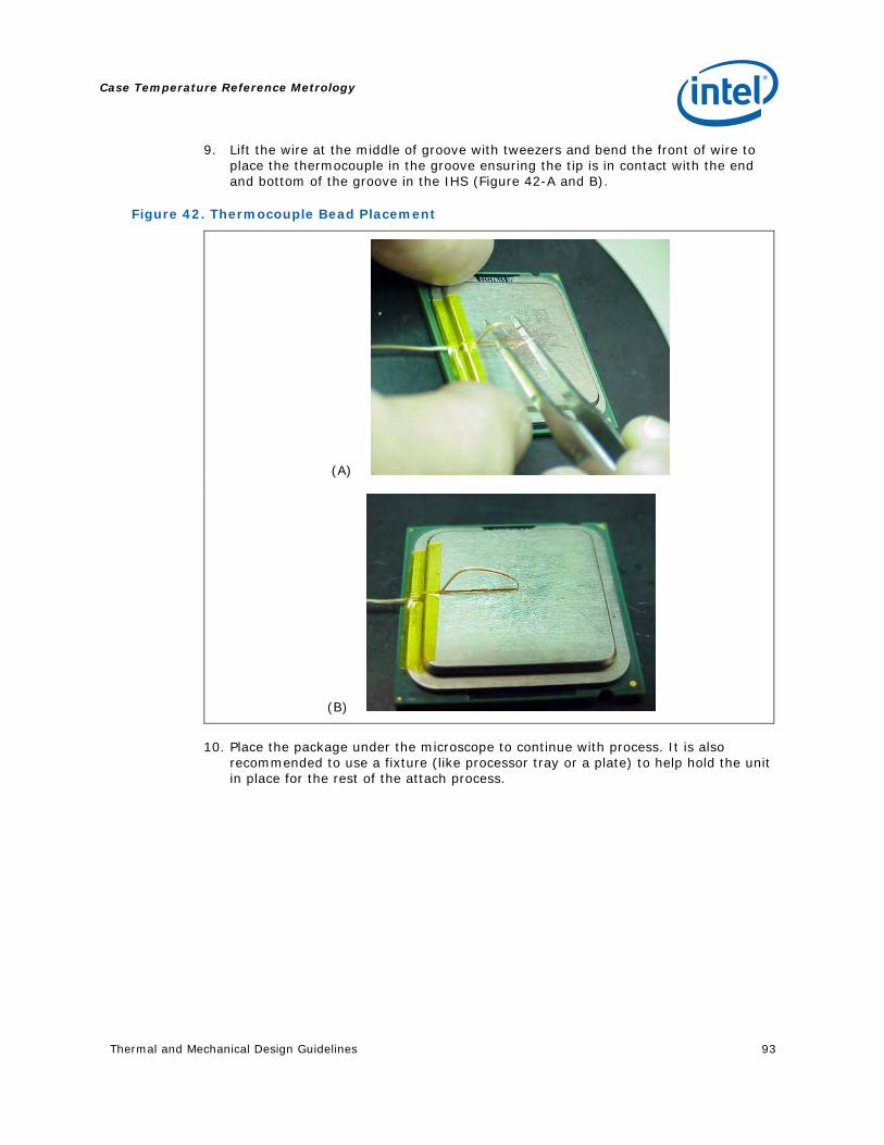
Case Temperature Reference Metrology
Thermal and Mechanical Design Guidelines 93
9. Lift the wire at the middle of groove with tweezers and bend the front of wire to place the thermocouple in the groove ensuring the tip is in contact with the end and bottom of the groove in the IHS (Figure 42-A and B).
Figure 42. Thermocouple Bead Placement
(A)
(B)
10. Place the package under the microscope to continue with process. It is also recommended to use a fixture (like processor tray or a plate) to help hold the unit in place for the rest of the attach process.

Case Temperature Reference Metrology
94 Thermal and Mechanical Design Guidelines
11. While still at the microscope, press the wire down about 6 mm [0.125”] from the thermocouple bead using the tweezers or your finger. Place a piece of Kapton* tape to hold the wire inside the groove (Figure 43). Refer to Figure 44 for detailed bead placement.
Figure 43. Position Bead on the Groove Step
Figure 44. Detailed Thermocouple Bead Placement
TC Wire with Insulation
IHS with Groove
TC Bead
Wire section into the groove to prepare for final bead placement
Kapton* tape

Case Temperature Reference Metrology
Thermal and Mechanical Design Guidelines 95
Figure 45. Third Tape Installation
12. Place a 3rd piece of tape at the end of the step in the groove as shown in Figure 45. This tape will create a solder dam to prevent solder from flowing into the larger IHS groove section during the melting process.
13. Measure resistance from thermocouple end wires (hold both wires to a DMM probe) to the IHS surface. This should be the same value as measured during the thermocouple conditioning in Section D.5.1.step 3 (Figure 46)
Figure 46. Measuring Resistance between Thermocouple and IHS
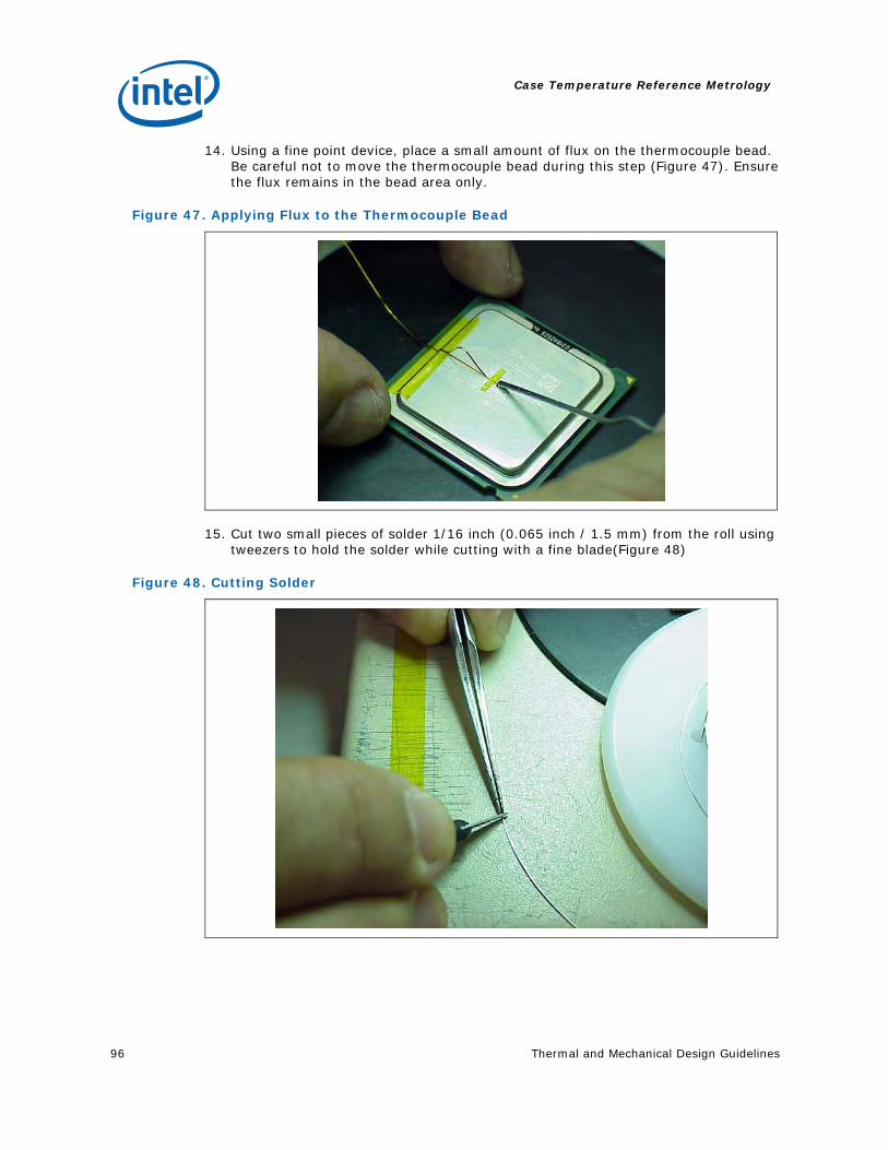
Case Temperature Reference Metrology
96 Thermal and Mechanical Design Guidelines
14. Using a fine point device, place a small amount of flux on the thermocouple bead. Be careful not to move the thermocouple bead during this step (Figure 47). Ensure the flux remains in the bead area only.
Figure 47. Applying Flux to the Thermocouple Bead
15. Cut two small pieces of solder 1/16 inch (0.065 inch / 1.5 mm) from the roll using tweezers to hold the solder while cutting with a fine blade(Figure 48)
Figure 48. Cutting Solder

Case Temperature Reference Metrology
Thermal and Mechanical Design Guidelines 97
16. Place the two pieces of solder in parallel, directly over the thermocouple bead (Figure 49)
Figure 49. Positioning Solder on IHS
17. Measure the resistance from the thermocouple end wires again using the DMM (refer to Section D.5.1.step 2) to ensure the bead is still properly contacting the IHS.
D.5.3 Solder Process 18. Make sure the thermocouple that monitors the Solder Block temperature is
positioned on the Heater block. Connect the thermocouple to a handheld meter to monitor the heater block temperature
19. Verify the temperature of the Heater block station has reached 155 °C ±5 °C before proceeding.
20. Connect the thermocouple for the device being soldered to a second hand-held meter to monitor IHS temperature during the solder process.

Case Temperature Reference Metrology
98 Thermal and Mechanical Design Guidelines
Figure 50. Solder Station Setup
21. Remove the land side protective cover and place the device to be soldered in the solder station. Make sure the thermocouple wire for the device being soldered is exiting the heater toward you.
Note: Don’t touch the copper heater block at any time as this is very hot.
22. Move a magnified lens light close to the device in the solder status to get a better view when the solder begins to melt.
23. Lower the Heater block onto the IHS. Monitor the device IHS temperature during this step to ensure the maximum IHS temperature is not exceeded
Note: The target IHS temperature during reflow is 150 °C ±3 °C. At no time should the IHS temperature exceed 155 °C during the solder process as damage to the device may occur.

Case Temperature Reference Metrology
Thermal and Mechanical Design Guidelines 99
24. You may need to move the solder back toward the groove as the IHS begins to heat. Use a fine tip tweezers to push the solder into the end of the groove until a solder ball is built up (Figure 51 and Figure 52)
Figure 51. View Through Lens at Solder Station
Figure 52. Moving Solder back onto Thermocouple Bead

Case Temperature Reference Metrology
100 Thermal and Mechanical Design Guidelines
25. Lift the heater block and magnified lens, using tweezers quickly rotate the device 90 degrees clockwise. Using the back of the tweezers press down on the solder; this will force out the excess solder
Figure 53. Removing Excess Solder
26. Allow the device to cool down. Blowing compressed air on the device can accelerate the cooling time. Monitor the device IHS temperature with a handheld meter until it drops below 50 °C before moving it to the microscope for the final steps.

Case Temperature Reference Metrology
Thermal and Mechanical Design Guidelines 101
D.5.4 Cleaning & Completion of Thermocouple Installation 27. Remove the device from the solder station and continue to monitor IHS
Temperature with a handheld meter. Place the device under the microscope and remove the three pieces of Kapton* tape with Tweezers, keeping the longest for re-use.
28. Straighten the wire and work the wire in to the groove. Bend the thermocouple over the IHS. Replace the long piece of Kapton* tape at the edge of the IHS.
Note: The wire needs to be straight so it does not sit above the IHS surface at anytime (Figure 54).
Figure 54. Thermocouple placed into groove

Case Temperature Reference Metrology
102 Thermal and Mechanical Design Guidelines
29. Using a blade carefully shave the excess solder above the IHS surface. Only shave in one direction until solder is flush with the groove surface (Figure 55).
Figure 55. Removing Excess Solder
Note: Take usual precautions when using open blades
30. Clean the surface of the IHS with alcohol and use compressed air to remove any remaining contaminants.
31. Fill the rest of the groove with Loctite* 498 Adhesive. Verify under the microscope that the thermocouple wire is below the surface along the entire length of the IHS groove (Figure 56)
Figure 56. Filling Groove with Adhesive
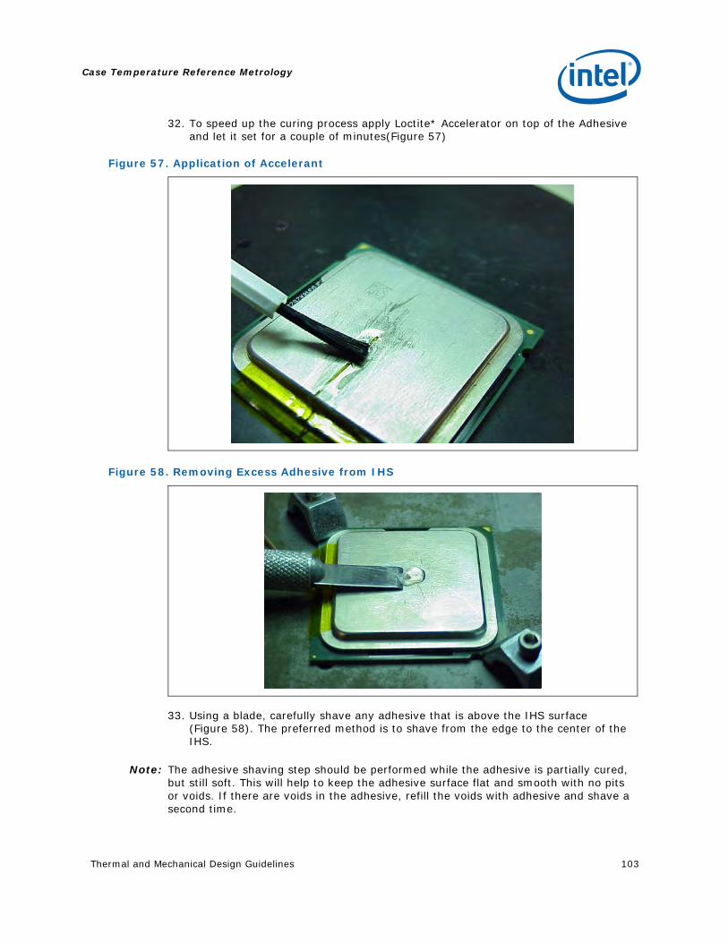
Case Temperature Reference Metrology
Thermal and Mechanical Design Guidelines 103
32. To speed up the curing process apply Loctite* Accelerator on top of the Adhesive and let it set for a couple of minutes(Figure 57)
Figure 57. Application of Accelerant
Figure 58. Removing Excess Adhesive from IHS
33. Using a blade, carefully shave any adhesive that is above the IHS surface (Figure 58). The preferred method is to shave from the edge to the center of the IHS.
Note: The adhesive shaving step should be performed while the adhesive is partially cured, but still soft. This will help to keep the adhesive surface flat and smooth with no pits or voids. If there are voids in the adhesive, refill the voids with adhesive and shave a second time.

Case Temperature Reference Metrology
104 Thermal and Mechanical Design Guidelines
34. Clean IHS surface with IPA and a wipe.
35. Clean the LGA pads with IPA and a wipe.
36. Replace the land side cover on the device.
37. Perform a final continuity test.
38. Wind the thermocouple wire into loops and secure or if provided by the vendor back onto the plastic roll. (Figure 59)
Figure 59. Finished Thermocouple Installation
39. Place the device in a tray or bag until it’s ready to be used for thermal testing use.
D.6 Thermocouple Wire Management
When installing the processor into the socket, make sure that the thermocouple wires exit above the load plate as Figure 60. Pinching the thermocouple wires between the load plate and the IHS will likely damage the wires.
Note: When thermocouple wires are damaged, the resulting reading maybe wrong. For example, if there are any cuts into the wires insulation where the wires are pinched between the IHS and the load plate, the thermocouple wires can get in contact at this location. In that case, the reported temperature would be the edge of the IHS/socket load plate area. This temperature is usually much lower than the temperature at the center of the IHS.
Prior to installing the heatsink, make sure that the thermocouple wires remain below the IHS top surface, by running a flat blade on top of the IHS for example.

Case Temperature Reference Metrology
Thermal and Mechanical Design Guidelines 105
Figure 60. Thermocouple Wire Management
§

Case Temperature Reference Metrology
106 Thermal and Mechanical Design Guidelines
Legacy Fan Speed Control
Thermal and Mechanical Design Guidelines 107
Appendix E Legacy Fan Speed Control
A motherboard design may opt to use a SIO or ASIC based fan speed control device that uses the existing look up or state based fan speed control.
The fan speed control implementations consist of the following items
• A motherboard designed with a fan speed controller with the following functionality: ⎯ PWM fan control output ⎯ Remote Digital thermal sensor measurement capability over the PECI bus for
Intel® Core™2 Duo desktop processor E6000/E4000 sequence and Intel® Pentium® Dual Core processor E2000 sequence.
⎯ SST thermal sensor to measure the on-die thermal diode for all earlier processors in the 775-land LGA package
• A motherboard with a 4 pin fan header for the processor heatsink fan.
• Processor heatsink with 4–wire PWM controlled Fan. A thermistor in the fan hub is recommended, but not a requirement. The reference solution and the Boxed Processor will implement a thermistor into the design.
The following sections discuss the necessary steps to implement Legacy Fan Speed Control.
Note: For the rest of this section the term “on-die thermal sensor” will be used interchangeably for the Digital thermal sensor or on-die thermal diode. On-die thermal diode will only be used when required for clarity.
E.1 Thermal Solution Design The first step is to select or design a processor thermal solution that meets the thermal profile for the processor. See Section 2.2.2 for the definition of the thermal profile and consult the processor datasheet for the specific values.
The designer needs to ensure that when the heatsink fan is operating at full speed the thermal solution will meet the TC-MAX limits at TDP. The slope of the thermal profile will allow the designer to make tradeoffs in thermal performance versus the inlet temperature to the processor fan heatsink.
E.1.1 Determine Thermistor Set Points A thermistor implemented in the hub of a fan is a first level of fan speed control. It provides an easy and cost effective means to begin acoustic noise reduction. It will, by design, run the fan at an appropriate speed based on the ambient conditions.
Chapter 5 and 6 discussed in detail the reference thermal solution, including the target ΨCA, and fan speed based on temperature to ensure that TC-MAX is not exceeded

Legacy Fan Speed Control
108 Thermal and Mechanical Design Guidelines
for TDP power at a given ambient temperature. The resulting variable speed fan (VSF) curve is the upper limit on fan speed.
The benefit of this upper limit will become more apparent when the fan speed controller is responding to the on-die thermal sensor.
Figure 61. Thermistor Set Points
Fan
Spe
ed(R
PM
)
Fan Inlet Temperature (°C)
Full Speed
30 38
Min. Operating
Variable Speed Fan (VSF) CurveFa
n S
peed
(RP
M)
Fan Inlet Temperature (°C)
Full Speed
30 38
Min. Operating
Variable Speed Fan (VSF) Curve
E.1.2 Minimum Fan Speed Set Point
The final aspect of thermal solution design is to determine the minimum speed the fan will be allowed to operate. This value can be driven by the cooling requirements for another portion of the design, such as the processor voltage regulator, or by functional limits of the fan design.
Per the Fan Specification for 4 wire PWM Controlled Fans; there are three possible options to consider
• Type A: The fan will run at minimum RPM for all PWM duty cycle values less than minimum duty cycle. This would be programmed into the fan controller located on the fan hub. It can not be overridden by the external fan speed control.
• Type B: The fan will run at minimum RPM for all non-zero PWM duty cycle values less than minimum duty cycle and turn off the fan at 0% PWM duty cycle.
• Type C: The fan will stop running when the current provided to the motor windings is insufficient to support commutation. The fan would turn off at 0% PWM duty cycle input.
For the reference thermal solution Type A was implemented.
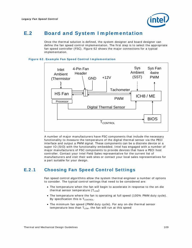
Legacy Fan Speed Control
Thermal and Mechanical Design Guidelines 109
E.2 Board and System Implementation
Once the thermal solution is defined, the system designer and board designer can define the fan speed control implementation. The first step is to select the appropriate fan speed controller (FSC). Figure 62 shows the major connections for a typical implementation.
Figure 62. Example Fan Speed Control Implementation
HS Fan
Processor
ICH8 / ME PWM
Tachometer
Digital Thermal Sensor
+12VGND
Sys Ambient (SST)
Sys Fan 4wire PWM
TCONTROLBIOS
Inlet Ambient
(Thermistor)
4-Pin Fan Header
A number of major manufacturers have FSC components that include the necessary functionality to measure the temperature of the digital thermal sensor via the PECI interface and output a PWM signal. These components can be a discrete device or a super IO (SIO) with the functionality embedded. Intel has engaged with a number of major manufacturers of FSC components to provide devices that have a PECI host controller. Contact your Intel Field Sales representative for the current list of manufacturers and visit their web sites or contact your local sales representatives for a part suitable for your design.
E.2.1 Choosing Fan Speed Control Settings
Fan speed control algorithms allow the system thermal engineer a number of options to consider. The typical control settings that need to be considered are:
• The temperature when the fan will begin to accelerate in response to the on-die thermal sensor temperature (TLOW)
• The temperature where the fan is operating at full speed (100% PWM duty cycle). By specification this is TCONTROL.
• The minimum fan speed (PWM duty cycle). For any on-die thermal sensor temperature less than TLOW, the fan will run at this speed

Legacy Fan Speed Control
110 Thermal and Mechanical Design Guidelines
These are the minimum parameters required to implement acoustic fan speed control. See Figure 63 for an example. There may be vendor specific options that offer enhanced functionality. See the appropriate vendor datasheet on how to implement those features.
Figure 63. Fan Speed Control
Diode Temperature (°C)
TCONTROL
Min Speed
Fan
Spe
ed
(RPM
)
Full Speed
TLOW
X %
Fan
Spe
ed
(% P
WM
Dut
y C
ycle
)
100 %
Diode Temperature (°C)
TCONTROL
Min Speed
Fan
Spe
ed
(RPM
)
Full Speed
TLOW
X %
Fan
Spe
ed
(% P
WM
Dut
y C
ycle
)
100 %
E.2.1.1 Temperature to Begin Fan Acceleration
The first item to consider is the value for TLOW. The FSC device needs a minimum temperature to set as the threshold to begin increasing PWM duty cycle to the fan.
The system designer might initially consider a small temperature range (TCONTROL – TLOW = TRANGE), 5 °C to accelerate the fan. That would delay the fan accelerating for the longest time after an increase in TSENSOR. There are a number of issues that should be considered with this strategy
• There is little granularity in the fan speeds. For each 1°C of increase in diode temperature = 20% jump in PWM duty cycle %
• Fan speed oscillation as the thermal solution chases the on-die thermal sensor temperature
• Having TSENSOR overshoot TCONTROL and the thermal profile causing the Thermal Control Circuit to activate to reduce the temperature.
• In extreme cases Thermtrip# activates and shuts down the processor
The first two cases can create a poor acoustic response for the user. The third case the user could notice a drop in performance as the thermal control circuit reduces the power. Figure 64 is an example of this situation. The system begins at idle and the Maxpower program is started at 65% workload.
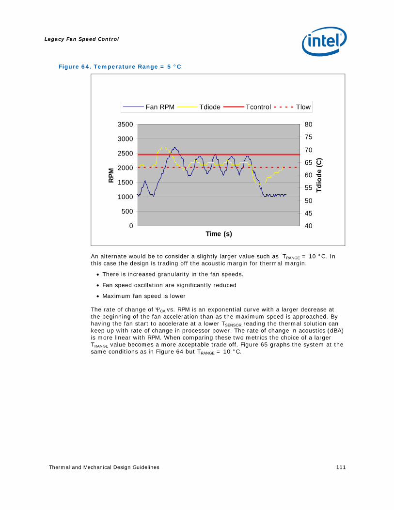
Legacy Fan Speed Control
Thermal and Mechanical Design Guidelines 111
Figure 64. Temperature Range = 5 °C
0
500
1000
1500
2000
2500
3000
3500
Time (s)
RPM
40
45
50
55
60
65
70
75
80
Tdio
de (C
)
Fan RPM Tdiode Tcontrol Tlow
An alternate would be to consider a slightly larger value such as TRANGE = 10 °C. In this case the design is trading off the acoustic margin for thermal margin.
• There is increased granularity in the fan speeds.
• Fan speed oscillation are significantly reduced
• Maximum fan speed is lower
The rate of change of ΨCA vs. RPM is an exponential curve with a larger decrease at the beginning of the fan acceleration than as the maximum speed is approached. By having the fan start to accelerate at a lower TSENSOR reading the thermal solution can keep up with rate of change in processor power. The rate of change in acoustics (dBA) is more linear with RPM. When comparing these two metrics the choice of a larger TRANGE value becomes a more acceptable trade off. Figure 65 graphs the system at the same conditions as in Figure 64 but TRANGE = 10 °C.

Legacy Fan Speed Control
112 Thermal and Mechanical Design Guidelines
Figure 65. Temperature Range = 10 °C
0
500
1000
1500
2000
2500
3000
3500
Time (s)
RPM
40
45
50
55
60
65
70
75
80
Tdio
de (C
)
Fan RPM Tdiode Tcontrol Tlow
It should be noted that having TSENSOR above TCONTROL is expected for workloads near TDP power levels and high system ambient. See Section E.4 for additional discussion on TCONTROL versus Thermal Profile
For use with the ATX Boxed Processor enabled reference solution a TRANGE value of 10 °C is recommended. For BTX Boxed processor enabled reference solutions TRANGE value of 7 °C is recommended.
E.2.1.2 Minimum PWM Duty Cycle
The final step in determining the FSC setting is to determine the minimum PWM Duty cycle. This is the fan speed for any TSENSOR < TLOW. The selection of this value is dependent on:
• Acoustic target at system idle
• Voltage regulator cooling
For a motherboard design intending to use the Boxed Processor or the enabled reference thermal solution, the recommended minimum PWM duty cycle is 20%.
Note: Set minimum PWM Duty Cycle only as low as required to meet acoustic requirements. The FSC design needs to accommodate transition from a low power state to TDP workloads without having Prochot# becoming active.
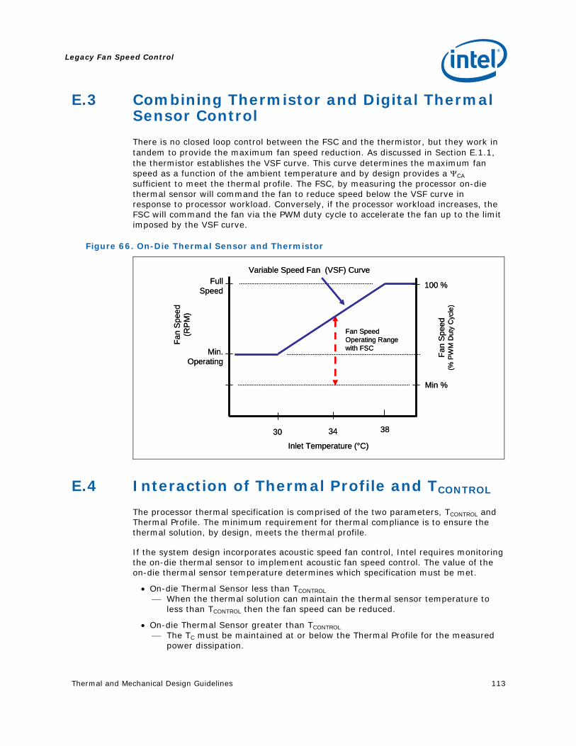
Legacy Fan Speed Control
Thermal and Mechanical Design Guidelines 113
E.3 Combining Thermistor and Digital Thermal Sensor Control
There is no closed loop control between the FSC and the thermistor, but they work in tandem to provide the maximum fan speed reduction. As discussed in Section E.1.1, the thermistor establishes the VSF curve. This curve determines the maximum fan speed as a function of the ambient temperature and by design provides a ΨCA sufficient to meet the thermal profile. The FSC, by measuring the processor on-die thermal sensor will command the fan to reduce speed below the VSF curve in response to processor workload. Conversely, if the processor workload increases, the FSC will command the fan via the PWM duty cycle to accelerate the fan up to the limit imposed by the VSF curve.
Figure 66. On-Die Thermal Sensor and Thermistor
Fan
Spee
d(R
PM
)
Inlet Temperature (°C)
Full Speed
30 38
Min. Operating
Variable Speed Fan (VSF) Curve
Fan Speed Operating Range with FSC
34
Min %
Fan
Spee
d
(% P
WM
Dut
y C
ycle
)
100 %
Fan
Spee
d(R
PM
)
Inlet Temperature (°C)
Full Speed
30 38
Min. Operating
Variable Speed Fan (VSF) Curve
Fan Speed Operating Range with FSC
34
Min %
Fan
Spee
d
(% P
WM
Dut
y C
ycle
)
100 %
E.4 Interaction of Thermal Profile and TCONTROL
The processor thermal specification is comprised of the two parameters, TCONTROL and Thermal Profile. The minimum requirement for thermal compliance is to ensure the thermal solution, by design, meets the thermal profile.
If the system design incorporates acoustic speed fan control, Intel requires monitoring the on-die thermal sensor to implement acoustic fan speed control. The value of the on-die thermal sensor temperature determines which specification must be met.
• On-die Thermal Sensor less than TCONTROL ⎯ When the thermal solution can maintain the thermal sensor temperature to
less than TCONTROL then the fan speed can be reduced.
• On-die Thermal Sensor greater than TCONTROL ⎯ The TC must be maintained at or below the Thermal Profile for the measured
power dissipation.

Legacy Fan Speed Control
114 Thermal and Mechanical Design Guidelines
To use all of the features in the Intel reference heatsink design or the Boxed processor, system integrators should verify the following functionality is present in the board design. Refer to the Fan Specification for 4 wire PWM Controlled Fans and Chapter 6 for complete details on the Intel enabled thermal solution.
The basics of Fan Speed Control were discussed in Chapter 7, as a review the FSC definitions are listed in Table 13.
Table 13. FSC Definitions
Item Definition
TSENSOR Temperature reported from the processor on-die thermal sensor.
TCONTROL TCONTROL is the specification limit for use with the on-die thermal sensor
TLOW The temperature above which the fan will begin to accelerate in response to the on-die thermal sensor temperature.
Hysteresis The number of degrees below TCONTROL the fans will remain on before slowing down.
THIGH The temperature at which the fan is operating at full speed (100% PWM Duty Cycle). By specification this is TCONTROL.
All Fans ON The processor temperature at which all fans in the system are increased to 100% Duty Cycle.
Min PWM Minimum pulse width modulation (% duty cycle) that the fans will run at when TSENSOR is less than TLOW.
Spin-up Amount of time fan is run at 100% duty cycle to overcome fan inertia.
PWM Freq The operating frequency of the PWM signal.
TAVERAGING The time (in seconds) that elapses while the fan is gradually sped up in response to a processor temperature spike.

Legacy Fan Speed Control
Thermal and Mechanical Design Guidelines 115
Figure 67. FSC Definition Example
Requirements Classification
• Required – an essential part of the design necessary to meet specifications. Should be considered a pass or fail in selection of a board.
• Suggested – highly desired for consistency among designs. May be specified or expanded by the system integrator.
The motherboard needs to have a fan speed control component that has the following characteristics:
• PWM output programmable to 21-28 kHz (required). PWM output set to 25 kHz (Suggested) as this value is the design target for the reference and for the Boxed Processor.
• External/remote thermal sensor measurement capability (required). Must support PECI and thermal diode via an SST device
• External/remote thermal sensor sampling rate ≥ 4 times per second (required).
• External/remote diode measurement (SST device) is calibrated by the component vendor to account for the diode ideality and package series resistance as listed in the appropriate datasheet.
Note: If the SST thermal sensor is not calibrated with the diode ideality and package series resistance, verify the board manufacturer has made provisions within the BIOS setup or other utility to input the corrections factors.

Legacy Fan Speed Control
116 Thermal and Mechanical Design Guidelines
The BIOS, at a minimum, must program the settings in Table 14 or Table 15, as appropriate, into the fan speed controller. The values are the minimum required to establish a fan speed control algorithm consistent with this document, the reference thermal solution, and Boxed processor thermal solution.
Table 14. ATX FSC Settings
Parameter Classification Processor Thermal Sensor
PWM Output Notes
THIGH Required TCONTROL 3
TLOW Required TCONTROL – 10 °C 3
Minimum PWM Duty Cycle
Required 20%
PWM Frequency Required 21–28 kHz 1
Spin-up time Suggested 250 - ~500 ms 2,4
TAVERAGING Suggested 35 sec 6
When TSENSOR < TLOW
Suggested Minimum PWM%
All Fans ON Suggested TCONTROL + 3 °C
Hysteresis Suggested 2 °C
NOTE: 1. A PWM frequency of 25 kHz is the design target for the reference and for the Intel®
Boxed processor and the reference design. 2. Use the lowest time available in this range for the device selected. 3. To ensure compliance with the thermal specification, thermal profile and usage of the
TSENSOR for fan speed control these setting should not be user configurable. 4. If this function is present on the device it must be enabled

Legacy Fan Speed Control
Thermal and Mechanical Design Guidelines 117
Table 15. Balanced Technology Extended (BTX) Fan Speed Control Settings
Parameter Classification Processor Thermal Sensor
System Ambient Sensor
PWM Output Notes
THIGH Required TCONTROL 54 °C 3,5
TLOW Required TCONTROL – 7 °C 47 °C 3,5
Minimum PWM Duty Cycle
Required PWM 1 (TMA) –20%
PWM Frequency Required 21–28 kHz 1
Spin Up Time Suggested 250 - ~ 500 ms 2, 7
TAVERAGING Suggested 4.0 sec 4.0 sec 3, 7
When TSENSOR < TLOW Suggested Minimum PWM%
Minimum PWM%
All Fans On Suggested TCONTROL + 3 °C 65 °C
Hysteresis Suggested 2 °C 4 °C
NOTE: 5. A PWM frequency of 25 kHz is the design target for the reference and for the Intel Boxed
processor and the reference design. 6. Use the lowest time available in this range for the device selected 7. TAVERAGING = represents the amount of delay time before responding to the temperature
change, defined in fan speed control device (sometimes called ramp range control or spike smoothing). Select the lowest setting available close to 4.0 seconds by the fan speed control device
8. The Fan Speed Controller, or Health Monitor Component, takes the result of the two fan speed ramps (processor and system) and drives the TMA fan to the highest resulting PWM duty cycle (%)
9. For BTX systems a second thermal sensor is recommended to capture chassis ambient for more detail see Appendix F.
10. To ensure compliance with the thermal specification, thermal profile, and usage of the TSENSOR for fan speed control these setting should not be user configurable.
11. If this function is present on the device it must be enabled.
Note: The fan speed component vendors provide libraries that are used by the BIOS writer to program the component registers with the parameters listed above. Consult the appropriate vendor datasheet for detailed information on programming their component.
§

Legacy Fan Speed Control
118 Thermal and Mechanical Design Guidelines

Balanced Technology Extended (BTX) System Thermal Considerations
Thermal and Mechanical Design Guidelines 119
Appendix F Balanced Technology Extended (BTX) System Thermal Considerations
There are anticipated system operating conditions in which the processor power may be low but other system component powers may be high. If the only Fan Speed Control (FSC) circuit input for the Thermal Module Assembly (TMA) fan is from the processor sensor then the fan speed and system airflow is likely to be too low in this operating state. Therefore, it is recommended that a second FSC circuit input be acquired from an ambient temperature monitor location within the system.
The location of the System Monitor thermal sensor is best determined through extensive system-level numerical thermal modeling or prototype thermal testing. In either case, the temperature of critical components or the air temperature near critical components should be assessed for a range of system external temperatures, component powers, and fan speed operating conditions. The temperature at the selected location for the System Monitor Point should be well correlated to the temperatures at or near critical components. For instance, it may be useful to monitor the temperature near the PSU airflow inlet, near the graphics add-in card, or near memory.
The final system integrator is typically responsible for ensuring compliance with the component temperature specifications at all operating conditions and, therefore, should be responsible for specifying the System Monitor thermal sensor location. However, it is not always possible for a board supplier – especially a channel board supplier – to know the system into which a board will be installed. It is, therefore, important for BTX board suppliers to select a System Monitor thermal sensor location that will function properly in most systems.
A BTX system should be designed such that the TMA exhaust is the primary airflow stream that cools the rest of the system. The airflow passes through the chipset heatsink and its temperature will rise as the memory controller chipset power increases. Since chipset power will increase when other subsystems (e.g. memory, graphics) are active, a System Monitor thermal sensor located in the exhaust airflow from the chipset heatsink is a reasonable location.
It is likely that a thermal sensor that is not mounted above the board and in the chipset exhaust airflow will reflect board temperature and not ambient temperature. It is therefore recommended that the Thermal sensor be elevated above the board.

Balanced Technology Extended (BTX) System Thermal Considerations
120 Thermal and Mechanical Design Guidelines
The thermal sensor location and elevation are reflected in the Flotherm thermal model airflow illustration and pictures (see Figure 68 and Figure 69).The Intel® Boxed Boards in BTX form factor have implemented a System Monitor thermal sensor. The following thermal sensor or its equivalent can be used for this function:
Part Number: C83274-002 BizLink USA Technology, Inc. 44911 Industrial Drive Fremont, CA 94538 USA (510)252-0786 phone (510)252-1178 fax [email protected]
Part Number: 68801-0170 Molex Incorporated 2222 Wellington Ct. Lisle, IL 60532 1-800-78MOLEX phone 1-630-969-1352 fax [email protected]
Figure 68. System Airflow Illustration with System Monitor Point Area Identified
OM16791
Power SupplyUnit
ThermalModule
MCHMemory
GraphicsAdd-In Card
Monitor Point

Balanced Technology Extended (BTX) System Thermal Considerations
Thermal and Mechanical Design Guidelines 121
Figure 69. Thermal sensor Location Illustration
TMA Airflow
Thermal Sensor
MCH Heatsink
§

Balanced Technology Extended (BTX) System Thermal Considerations
122 Thermal and Mechanical Design Guidelines

Mechanical Drawings
Thermal and Mechanical Design Guidelines 123
Appendix G Mechanical Drawings
The following table lists the mechanical drawings included in this appendix. These drawings refer to the reference thermal mechanical enabling components for the processor.
Note: Intel reserves the right to make changes and modifications to the design as necessary.
Drawing Description Page Number
ATX/µATX Motherboard Keep-out Footprint Definition and Height Restrictions for Enabling Components – Sheet 1
124
ATX/µATX Motherboard Keep-out Footprint Definition and Height Restrictions for Enabling Components – Sheet 2
125
ATX/µATX Motherboard Keep-out Footprint Definition and Height Restrictions for Enabling Components – Sheet 3
126
. Balanced Technology Extended (BTX) Thermal Module Keep Out Volumetric – Sheet 1
127
Balanced Technology Extended (BTX) Thermal Module Keep Out Volumetric – Sheet 2
128
. Balanced Technology Extended (BTX) Thermal Module Keep Out Volumetric – Sheet 3
129
Balanced Technology Extended (BTX) Thermal Module Keep Out Volumetric – Sheet 4
130
Balanced Technology Extended (BTX) Thermal Module Keep Out Volumetric – Sheet 5
131
ATX Reference Clip – Sheet 1 132
ATX Reference Clip – Sheet 2 133
Reference Fastener – Sheet 1 134
Reference Fastener – Sheet 2 135
Reference Fastener – Sheet 3 136
Reference Fastener – Sheet 4 137
Intel® RCFH4 Reference Solution Assembly 138
Intel® RCFH4 Reference Solution Assembly – Sheet 2 139

M
ech
an
ical D
raw
ing
s
124
Ther
mal
and M
echan
ical
Des
ign G
uid
elin
es
Fig
ure
70
. A
TX
/µ
ATX
Mo
therb
oard
Keep
-ou
t Fo
otp
rin
t D
efi
nit
ion
an
d H
eig
ht
Rest
rict
ion
s fo
r En
ab
lin
g C
om
po
nen
ts –
Sh
eet
1
BCD A
12
34
56
78
47.50
47.50
2
0.00
2 0.0039
.01
21.00
20.00
28.00
36.78
41.00
36.00
31.51
23.00
15.50
15.50
23.00
31.51
31.51
36.78
45.26
31.96
45.26
19.32
19.32
47.5045.26
36.49
27.00
36.78
23.47
23.47
36.78
45.26
40.00
27.81
32.5127.51
32.51
27.51
47.50
4X
4.03
36.00
36.00
24.516.15
5.90
7.30
7.05
13.00 2.2
0
33.00
44.0040.00 39.01
39.01
39.01
36.00
36.00
()
17.44
PIN 1
()
16.96
5
()
1.17
()
1.09
()
1.93
()
2.80
()
1.09
()
1.17
4X
6.00
()
37.50
()
37.50
()
95.00
()
72.00
()
95.00
()
72.00
()
0.965
()
0.570
()
16.00
() 16.87
()
20.00
()
19.13
LEGE
NDSO
CKET
/THER
MO/M
ECHA
NICA
L COM
PONE
NT KE
EP-IN
S
10.0
MM M
AX C
OMPO
NENT
HEIG
HT
2.5 M
M MA
X COM
PONE
NT H
EIGHT
6.0 M
M MA
X COM
PONE
NT H
EIGHT
25.0
MM M
AX C
OMPO
NENT
HEIG
HT
1.8 M
M MA
X COM
PONE
NT H
EIGHT
BOAR
D RO
UTIN
G KE
EP-O
UT
SHEE
T 1
OF
3DO
NOT
SCAL
E DRA
WING
SCAL
E: N
ONE
3C4
0819
D
REV
DRAW
ING
NUM
BER
CAG
E CO
DESIZ
E
LGA7
75 m
icroA
TXCO
MPON
ENT K
EEP-
INS
TITL
E
2200
MIS
SION
COL
LEGE
BLV
D.P.
O. B
OX 58
119
SANT
A CL
ARA,
CA
9505
2-811
9CO
RP.
RDE
PART
MEN
T
N/A
FINI
SH:
N/A
MAT
ERIA
L:
DATE
APPR
OVE
D BY
DATE
APPR
OVE
D BY
DATE
CHEC
KED
BY
DATE
DESI
GNE
D BY
UNL
ESS O
THER
WISE
SPEC
IFIED
IN
TERP
RET D
IMEN
SION
S AN
D TO
LERA
NCES
IN AC
CORD
ANCE
WITH
ASM
E Y1
4.5M-
1994
DIME
NSIO
NS A
RE IN
MILL
IMET
ERS
THIR
D AN
GLE
PROJ
ECTIO
N
REVI
SION
HIS
TORY
ZONE
REV
DESC
RIPT
ION
DATE
APPR
OVED
NOTE
S:1.
DIME
NSIO
NS AR
E IN
MILL
IMET
ERS.
2 G
EOME
TRIC
CEN
TER
OF C
PU PA
CKAG
E / S
OCKE
T HOU
SING
CAVIT
Y.3.
BOAR
D CO
MPON
ENET
KEEP
-INS
AND
MECH
ANIC
AL C
OMPO
NENE
T KEE
P-OU
TS
TO
BE U
TILIZE
D WI
TH SU
FFIC
IENT A
LLOW
ANCE
S FO
R PL
ACEM
ENT A
ND S
IZE TO
LERA
NCES
, A
SSEM
BLY
PROC
ESS
ACCE
SS, A
ND D
YNAM
IC E
XCUR
SION
S.4.
ASSU
ME SY
MMET
RY FO
R UN
DIME
NSIO
NED
CORN
ERS A
ND ED
GES.
DETA
IL A
BOAR
D PRIM
ARY S
IDE
PACK
AGE
BOUN
DARY
SOCK
ET BA
LL 1
SOCK
ET VO
LOU
TLINE
SEE D
ETAIL
A
SOCK
ET B
ALLS
PACK
AGE L
ANDS
SOCK
ET BA
LL 1
SOCK
ET H
OUSIN
GCA
VITY
PACK
AGE B
OUND
ARY
PIN 1

M
ech
an
ical D
raw
ing
s
Ther
mal
and M
echan
ical
Des
ign G
uid
elin
es
125
Fig
ure
71
. A
TX
/µ
ATX
Mo
therb
oard
Keep
-ou
t Fo
otp
rin
t D
efi
nit
ion
an
d H
eig
ht
Rest
rict
ion
s fo
r En
ab
lin
g C
om
po
nen
ts –
Sh
eet
2
13
45
67
8
BCD A
12
34
56
78
BCD A
THIS
DRA
WIN
G CO
NTAI
NS IN
TEL C
ORPO
RAT
ION
CONF
IDEN
TIAL I
NFOR
MATIO
N. IT
IS
DISC
LOSE
D IN
CON
FIDEN
CE A
ND IT
S CO
NTEN
TSMA
Y NO
T BE
DISC
LOSE
D, R
EPRO
DUCE
D, D
ISP
LAYE
D OR
MOD
IFIED
, WITH
OUT T
HE P
RIOR
WRI
TTEN
CON
SENT
OF I
NTEL
COR
PORA
TIO
N.
4X
6.00
4X
10.00
LEGE
NDCO
MPON
ENT K
EEP-
OUT
ROUT
ING
KEEP
-OUT
SHEE
T 2
OF
3DO
NOT
SCAL
E DRA
WING
SCAL
E: N
ONE
2200
MIS
SION
COL
LEGE
BLV
D.P.
O. B
OX 58
119
SANT
A CL
ARA,
CA
9505
2-811
9CO
RP.
R
TMD
3C4
0819
D
REV
DRAW
ING
NUM
BER
CAG
E CO
DESIZ
EDE
PART
MEN
T
C408
192
3DW
G. N
OSH
T.RE
V
SOCK
ET BA
LL 1
COMP
ONEN
T VOL
UMET
RIC
KEEP
-INS
ROUT
ING KE
EP-O
UTS
SOCK
ET &
PROC
ESSO
RVO
LUME
TRIC
KEEP
-IN O
UTLIN
E
BOAR
D SE
COND
ARY S
IDE
SOCK
ET B
ALL 1
(FAR
SID
E)
SOCK
ET &
PROC
ESSO
RVO
LUME
TRIC
KEEP
-IN

M
ech
an
ical D
raw
ing
s
126
Ther
mal
and M
echan
ical
Des
ign G
uid
elin
es
Fig
ure
72
. A
TX
/µ
ATX
Mo
therb
oard
Keep
-ou
t Fo
otp
rin
t D
efi
nit
ion
an
d H
eig
ht
Rest
rict
ion
s fo
r En
ab
lin
g C
om
po
nen
ts –
Sh
eet
3
13
45
67
8
BCD A
12
34
56
78
BCD A
THIS
DRA
WIN
G CO
NTAI
NS IN
TEL C
ORPO
RAT
ION
CONF
IDEN
TIAL I
NFOR
MATI
ON. IT
IS
DISC
LOSE
D IN
CON
FIDE
NCE
AND
ITS
CONT
ENTS
MAY
NOT
BE D
ISCL
OSED
, REP
RODU
CED,
DI
SPLA
YED
OR M
ODIF
IED,
WIT
HOUT
THE
PRI
OR W
RITT
EN C
ONSE
NT O
F INT
EL C
ORPO
RAT
ION.
A
A
5.80
5.80
3.00
2.75
3.80
30.00
R49.4
4
R33.2
9
2
8.15
27.25
3.00
19.25
37.00
29.00
32.85
24.50
49.00
2X 45 X
3.00
45 X
3.50
2.50
3.00
14.10
14.60
6.60
6.60
3.80
120.0 1.0
0
()
37.60
()
37.60
()
16.87
()
16.00
()
46.11
()
55.58
SHEE
T 3
OF
3DO
NOT
SCAL
E DRA
WING
SCAL
E: N
ONE
2200
MIS
SION
COL
LEGE
BLV
D.P.
O. B
OX 58
119
SANT
A CL
ARA,
CA
9505
2-811
9CO
RP.
R
TMD
3C4
0819
D
REV
DRAW
ING
NUM
BER
CAG
E CO
DESIZ
EDE
PART
MEN
T
C408
193
3DW
G. N
OSH
T.RE
V
LEVE
R MO
TION
SPAC
ERE
QUIR
ED TO
REL
EASE
SOCK
ET LO
AD PL
ATE
NOTE
S:1
SOCK
ET C
ENTE
R PL
ANES
ARE R
EFER
ENCE
D FR
OM G
EOME
TRIC
CEN
TER
OF SO
CKET
HOU
SING
CAVIT
Y FOR
CPU
PACK
AGE (
ALIG
NES
WITH
DAT
UM R
EFER
ENCE
GIVE
N FO
R BO
ARD
COMP
ONEN
T KEE
P-IN
S).
2 SO
CKET
KEEP
-IN VO
LUME
VERT
ICAL
HEIG
HT ES
TABL
ISHES
LIMI
T OF S
OCKE
T A
ND C
PU PA
CKAG
E ASS
EMBL
Y IN
THE S
OCKE
T LOC
KED
DOW
N PO
SITIO
N. I
T ENC
OMPA
SSES
SOCK
ET AN
D CP
U PA
CKAG
E DIM
ENSIO
NAL T
OLER
ANCE
S A
ND D
EFLE
CTIO
N / S
HAPE
CHA
NGES
DUE
TO D
SL LO
AD.
3. SO
CKET
KEEP
-IN VO
LUME
ENCO
MPAS
S THE
SOCK
ET N
OMIN
AL VO
LUME
AN
D AL
LOWA
NCES
FOR
SIZE T
OLER
ANCE
S. TH
ERMA
L/MEC
HANI
CAL C
OMPO
NENT
DEV
ELOP
ERS S
HALL
DES
IGN
TO TH
E OUT
SIDE O
F SOC
KET K
EEP I
N VO
LUME
WITH
CLE
ARAN
CE M
ARGI
NS. S
OCKE
T DEV
ELOP
ERS S
HALL
DES
IGN
TO TH
E INS
IDE V
OLUM
E.
SOCK
ET &
PROC
ESSO
R VOL
UMET
RIC KE
EP-IN
TOP S
IDE V
IEWBO
TTOM
SIDE
VIEW
1SO
CKET
HOU
SING
1CA
VITY (
CPU
PACK
AGE)
SOCK
ET BA
LL 1
LEVE
R MO
TION
SPAC
ERE
QUIR
ED TO
REL
EASE
SOCK
ET LO
AD PL
ACE
(FARS
IDE)
SECT
ION
A-A

M
ech
an
ical D
raw
ing
s
Ther
mal
and M
echan
ical
Des
ign G
uid
elin
es
127
Fig
ure
73
. B
ala
nce
d T
ech
no
log
y E
xte
nd
ed
(B
TX
) Th
erm
al M
od
ule
Keep
Ou
t V
olu
metr
ic –
Sh
eet
1
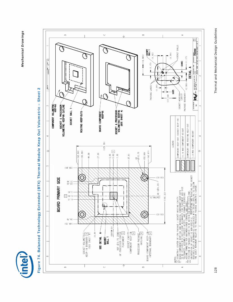
M
ech
an
ical D
raw
ing
s
128
Ther
mal
and M
echan
ical
Des
ign G
uid
elin
es
Fig
ure
74
. B
ala
nce
d T
ech
no
log
y E
xte
nd
ed
(B
TX
) Th
erm
al M
od
ule
Keep
Ou
t V
olu
metr
ic –
Sh
eet
2

M
ech
an
ical D
raw
ing
s
Ther
mal
and M
echan
ical
Des
ign G
uid
elin
es
129
Fig
ure
75
. B
ala
nce
d T
ech
no
log
y E
xte
nd
ed
(B
TX
) Th
erm
al M
od
ule
Keep
Ou
t V
olu
metr
ic –
Sh
eet
3

M
ech
an
ical D
raw
ing
s
130
Ther
mal
and M
echan
ical
Des
ign G
uid
elin
es
Fig
ure
76
. B
ala
nce
d T
ech
no
log
y E
xte
nd
ed
(B
TX
) Th
erm
al M
od
ule
Keep
Ou
t V
olu
metr
ic –
Sh
eet
4

M
ech
an
ical D
raw
ing
s
Ther
mal
and M
echan
ical
Des
ign G
uid
elin
es
131
Fig
ure
77
. B
ala
nce
d T
ech
no
log
y E
xte
nd
ed
(B
TX
) Th
erm
al M
od
ule
Keep
Ou
t V
olu
metr
ic –
Sh
eet
5
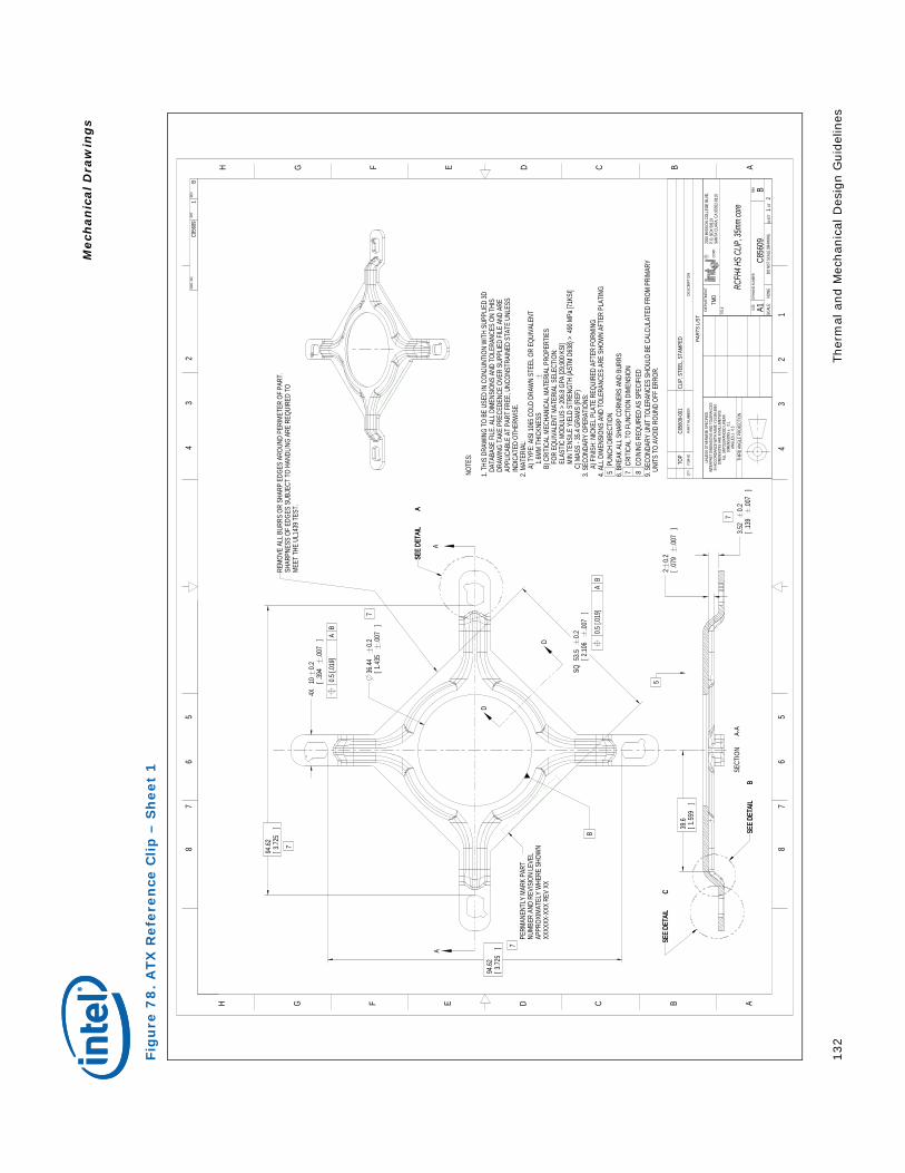
M
ech
an
ical D
raw
ing
s
132
Ther
mal
and M
echan
ical
Des
ign G
uid
elin
es
Fig
ure
78
. A
TX
Refe
ren
ce C
lip
– S
heet
1
8
7
6
5
4
3
2
H G F E D C B A
8
7
6
5
4
3
2
1
H G F E D C B A
AA
20.2
.079
.007
[] 3.5
20.2
.139
.007
[]
94.62 3.7
25[
]
SQ 5
3.50.2
2.106
.007
[]
94.62 3.7
25[
]
4X
100.2
.394
.007
[]
39.6 1.5
59[
]
7
36.44
0.21.4
35.00
7[
]
B
C856
091
BDW
G. N
OSH
T.RE
V
DEP
ARTM
ENT
R CORP
.
2200
MIS
SION
COL
LEGE
BLV
D.P.
O. B
OX 58
119
SANT
A CL
ARA,
CA
9505
2-81
19TM
D TI
TLE
RCFH
4 HS C
LIP, 3
5mm
core
SIZE
DRA
WIN
G NU
MBER
REV
A1C8
5609
BSC
ALE:
NO
NEDO
NOT
SCA
LE D
RAW
ING
SHEE
T 1
OF
2
UNLE
SS O
THER
WIS
E SP
ECIF
IED
INTE
RPRE
T DI
MENS
IONS
AND
TOL
ERAN
CES
IN A
CCOR
DANC
E W
ITH
ASME
Y14
.5M-1
994
DIME
NSIO
NS A
RE IN
MILL
IMET
ERS
ALL U
NTOL
ERAN
CED
LINEA
RDI
MENS
IONS
±0.1
ANGL
ES ±
0.5TH
IRD
ANGL
E PR
OJEC
TION
PART
S LI
ST
DES
CR
IPTI
ON
PAR
T N
UM
BER
ITEM
NOQT
Y
CLIP
, STE
EL, S
TAMP
EDC8
5609
-001
TOP
0.5 [.0
19]
AB
7
7
0.5 [.0
19]
AB
NOT
ES:
1. TH
IS D
RAW
ING
TO B
E US
ED IN
CON
JUNT
ION
WIT
H SU
PPLIE
D 3D
DAT
ABAS
E FI
LE. A
LL D
IMEN
SION
S AN
D TO
LERA
NCES
ON
THIS
DRA
WIN
G TA
KE P
RECE
DENC
E OV
ER S
UPPL
IED
FILE
AND
ARE
A
PPLIC
ABLE
AT
PART
FRE
E, U
NCON
STRA
INED
STA
TE U
NLES
S I
NDIC
ATED
OTH
ERW
ISE.
2. MA
TERI
AL:
A
) TYP
E: A
ISI 1
065 C
OLD
DRAW
N ST
EEL O
R EQ
UIVA
LENT
1.6MM
THI
CKNE
SS
B
) CRI
TICA
L MEC
HANI
CAL M
ATER
IAL P
ROPE
RTIE
S
FO
R EQ
UIVA
LENT
MAT
ERIA
L SEL
ECTI
ON:
ELAS
TIC
MODU
LUS
> 206
.8 GP
A [29
,900 K
SI]
MIN
TENS
ILE Y
IELD
STR
ENGT
H (A
STM
D638
) > 4
90 M
Pa [7
1KSI
]
C) M
ASS
- 35.4
GRA
MS (R
EF)
3. SE
COND
ARY
OPER
ATIO
NS:
A
) FIN
ISH:
NIC
KEL P
LATE
REQ
UIRE
D AF
TER
FORM
ING
4. AL
L DIM
ENSI
ONS
AND
TOLE
RANC
ES A
RE S
HOW
N AF
TER
PLAT
ING
5 P
UNCH
DIR
ECTI
ON6.
BREA
K AL
L SHA
RP C
ORNE
RS A
ND B
URRS
7 C
RITI
CAL T
O FU
NCTI
ON D
IMEN
SION
8 C
OINI
NG R
EQUI
RED
AS S
PECI
FIED
9. SE
COND
ARY
UNIT
TOL
ERAN
CES
SHOU
LD B
E CA
LCUL
ATED
FRO
M PR
IMAR
Y U
NITS
TO
AVOI
D RO
UND
OFF
ERRO
R.5
7
REMO
VE A
LL B
URRS
OR
SHAR
P ED
GES
AROU
ND P
ERIM
ETER
OF
PART
.SH
ARPN
ESS
OF E
DGES
SUB
JECT
TO
HAND
LING
ARE
REQU
IRED
TO
MEET
THE
UL1
439 T
EST.
PERM
ANEN
TLY
MARK
PAR
TNU
MBER
AND
REV
ISIO
N LE
VEL
APPR
OXIM
ATEL
Y W
HERE
SHO
WN
XXXX
XX-X
XX R
EV X
X
SEE
DETA
IL
A
SECT
ION
A-
A
SEE
DETA
IL
C
SEE
DETA
IL
B
SEE
DETA
IL
A
SEE
DETA
IL
C
SEE
DETA
IL
B
D
D

M
ech
an
ical D
raw
ing
s
Ther
mal
and M
echan
ical
Des
ign G
uid
elin
es
133
Fig
ure
79
. A
TX
Refe
ren
ce C
lip
– S
heet
2
H G F E D C B A
H G F E D C B A
8
7
6
5
4
3
2
8
7
6
5
4
3
2
1
5.3 .209
[]
1.65 .06
5[
]
7.35 .28
9[
]
2X
R3.6 .14
2[
]
RTY
P0.3 .01
2[
]
2X
R0.5 .02
0[
]
7.31 .28
8[
]
135
1.06 .04
2[
]
2.97 .11
7[
]
133.5
9
R1.4 .05
5[
]
R3.1 .12
2[
]
45 X
80.4
50.0
5.01
8.00
1[
]
45 X
80.2
50.0
5.01
0.00
1[
]
C856
092
0DW
G. N
OSH
T.RE
V
DEP
ARTM
ENT
R CORP
.
2200
MIS
SION
COL
LEGE
BLV
D.P.
O. B
OX 58
119
SANT
A CL
ARA,
CA
9505
2-81
19TM
D
SIZE
DRA
WIN
G NU
MBER
REV
A1C8
5609
0SC
ALE:
1
DO N
OT S
CALE
DRA
WIN
GSH
EET
2 OF
2
DETA
IL
ASC
ALE
10
TYPI
CAL 4
PLA
CES
0.1 [.0
03]
AB
0.2 [.0
07]
AB
DETA
IL
CSC
ALE
10
TYP
4 PLA
CES
DETA
IL
BSC
ALE
20
THIS
POI
NT C
ORRE
SPON
DS T
O TH
E 39
.6DI
MENS
ION
ON S
HEET
1 ZO
NE A
7
0.4 [.0
15]
AB
0.5 [.0
19]
AB
SECT
ION
D-
DSC
ALE
8
7BO
UNDA
RY
W
X
WX
4X
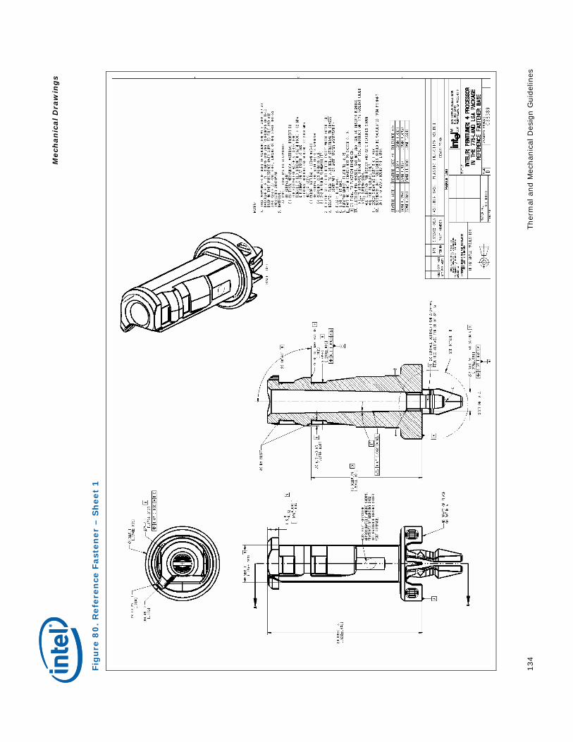
M
ech
an
ical D
raw
ing
s
134
Ther
mal
and M
echan
ical
Des
ign G
uid
elin
es
Fig
ure
80
. R
efe
ren
ce F
ast
en
er
– S
heet
1

M
ech
an
ical D
raw
ing
s
Ther
mal
and M
echan
ical
Des
ign G
uid
elin
es
135
Fig
ure
81
. R
efe
ren
ce F
ast
en
er
– S
heet
2

M
ech
an
ical D
raw
ing
s
136
Ther
mal
and M
echan
ical
Des
ign G
uid
elin
es
Fig
ure
82
. R
efe
ren
ce F
ast
en
er
– S
heet
3
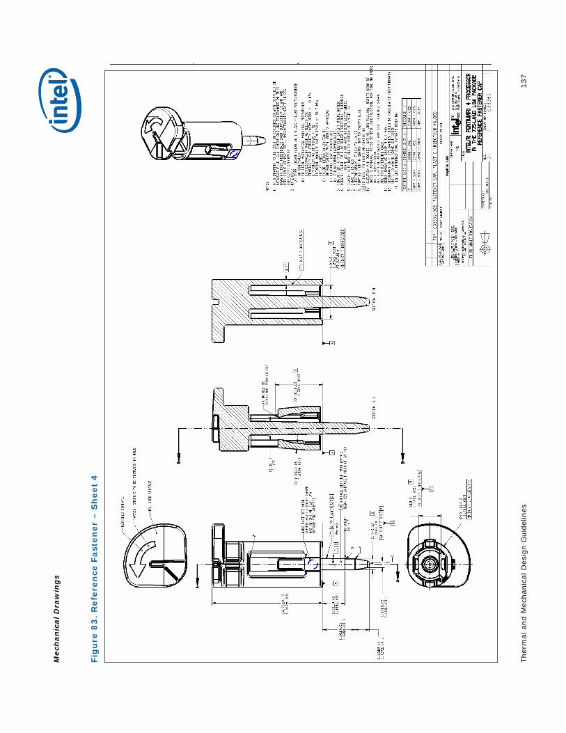
M
ech
an
ical D
raw
ing
s
Ther
mal
and M
echan
ical
Des
ign G
uid
elin
es
137
Fig
ure
83
. R
efe
ren
ce F
ast
en
er
– S
heet
4

M
ech
an
ical D
raw
ing
s
138
Ther
mal
and M
echan
ical
Des
ign G
uid
elin
es
Fig
ure
84
. In
tel®
RC
FH
4 R
efe
ren
ce S
olu
tio
n A
ssem
bly
()
120 4.7[
]
()
95 3.740
[]
()
90 3.543
[]
()
65.42 2.5
76[
] ()
62.9 2.4
76[
]
DEP
ARTM
ENT
R CORP
.
2200
MIS
SION
COL
LEGE
BLV
D.P.
O. B
OX 58
119
SANT
A CLA
RA, C
A 95
052-8
119
TMD
TITL
E
RCFH
4, MA
IN AS
SEMB
LYSIZ
E D
RAWI
NG N
UMBE
RRE
V
A1C8
8300
ASC
ALE:
1DO
NOT S
CALE
DRAW
ING
SHEE
T 1
OF
2SE
E NO
TES
SEE
NOTE
SFIN
ISHMA
TERI
AL09
/23/04
DATE
APPR
OVED
BY09
/23/04
09/23
/04DA
TECH
ECKE
D BY
09/21
/04DA
TEDR
AWN
BY09
/21/04
DATE
DESIG
NED
BYUN
LESS
OTH
ERW
ISE
SPEC
IFIED
INTE
RPRE
T DIM
ENSI
ONS
AND
TOLE
RANC
ESIN
ACC
ORDA
NCE
WITH
ASM
E Y1
4.5M-
1994
DIME
NSIO
NS A
RE IN
MILL
IMET
ERS
ALL U
NTOL
ERAN
CED
LINEA
RDI
MENS
IONS
±0
ANGL
ES ±
0.5TH
IRD
ANGL
E PR
OJEC
TION
PART
S LI
ST
DES
CR
IPTI
ON
PAR
T N
UM
BER
ITEM
NOQT
Y
RCFH
4,MAI
N AS
SEMB
LYC8
8300
-001
TOP
PRES
COTT
FMB2
FAN
ATT
ACH
C364
48-00
11
1RC
FH4,G
UARD
,WIR
EC8
7023
-001
21
RCH4
,FAN
ASSE
MBLY
C882
97-00
13
1RC
H4,H
S,CL
IP,C
ORE,
FAST
ENER
SC8
8298
-001
41
NOTE
S:1.
FOR
DETA
ILED
SPEC
IFICA
TIONS
SEE
COM
PONE
NT D
RAW
INGS
.2.
THER
MAL I
NTER
FACE
MAT
ERIA
L: 0.2
CC (0
.4 GR
AMS)
SHI
N-ET
SU-M
ICRO
-S1
G75
1 THE
RMAL
GRE
ASE.
3. SE
E SH
EET 2
FOR
ASSE
MBLY
REC
OMME
NDAT
IONS
.4.
US P
ATEN
TS P
ENDI
NG.
1
2
3
4
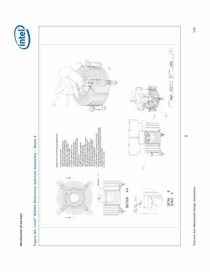
M
ech
an
ical D
raw
ing
s
Ther
mal
and M
echan
ical
Des
ign G
uid
elin
es
139
Fig
ure
85
. In
tel®
RC
FH
4 R
efe
ren
ce S
olu
tio
n A
ssem
bly
– S
heet
2
AA
9.53
0.12
.375
.004
[]
()
9.53 .37
5[
]
()
5.88 .23
2[
]
DEP
ARTM
ENT
R CORP
.
2200
MIS
SION
COL
LEGE
BLV
D.P.
O. B
OX 58
119
SANT
A CL
ARA,
CA
9505
2-811
9-
SIZE
DRA
WING
NUM
BER
REV
A1C8
8300
ASC
ALE:
1DO
NOT
SCAL
E DRA
WING
SHEE
T 2 O
F 2
ASSE
MBLY
/INST
ALLA
TION
PROC
ESS
RECO
MMEN
DATIO
NS 1
FAN
ATTA
CH IN
STAL
LATIO
N: I
NSER
T FAN
ATT
ACH
(1) IN
TO H
EAT S
INK
(4) T
O TH
E SP
ECIFI
ED D
EPTH
AND
ORI
ENTA
TION.
INS
ERT T
OOL T
O KE
Y TO
TOP
OF H
EAT S
INK
FOR
DEP
TH A
CCUR
ACY.
ARB
OR P
RESS
OR
SIMI
LAR
TOOL
IS R
EQUI
RED.
2 FA
N AN
D FA
N WI
RE IN
STAL
LATIO
N: A
. THR
EAD
WIR
ES TH
ROUG
H FIN
GAP
ON
HEA
T SIN
K FIN
S (4)
AND
POS
ITION
THEM
FLAT
ACR
OSS
POCK
ET C
UT A
ND D
OWN
SPAC
E W
HERE
HAL
F LEN
GTH
FIN IS
. B
. LOW
ER TH
E FA
N (2)
WHI
LE TH
READ
ING
WIR
ES TH
ROUG
H TH
E HE
AT S
INK
(4).
C. T
O SN
AP FA
N IN
TO TH
E HE
AT S
INK
APP
LY A
PPRO
XIMA
TELL
Y 14
N (3
.2 LB
F) O
F FOR
CE W
ITH TH
E TO
OL TH
AT IN
TERF
ACES
WITH
FAN
STA
TOR
THRO
UGH
THE
THRE
E HO
LES
ON
THE
FAN
IMPE
LLER
. NOT
E: P
RESS
ING
DIRE
CTLY
ON
THE
FAN
IMPE
LLER
MAY
CAU
SE D
AMAG
E T
O IN
TERN
AL FA
N CO
MPON
ENTS
.3
INSE
RT FA
NGUA
RD (3
) TO
2 ADJ
ACEN
T CUT
S ON
HEA
T S
INK
AND
SIMU
TANI
OUSL
Y SP
READ
REM
AINI
NG FA
NGUA
RD LE
GS
TO
CLEA
R FA
N AN
D EX
TRUS
ION
AND
ROTA
TE G
UARD
TO E
NGUA
GE R
EMAI
NING
CUT
S IN
HEA
TSIN
K.4
CRI
TICAL
TO FU
NCTIO
N.
3
3
3
41
2
2
SECT
ION
A-
A
SEE
DETA
IL
B
DETA
IL
BSC
ALE
6
§

Intel® Currently Enabled Reference Solution Information
140 Thermal and Mechanical Design Guidelines
Appendix H Intel® Currently Enabled Reference Solution Information
This appendix includes supplier information for Intel enabled vendors.
The reference component designs are available for adoption by suppliers and heatsink integrators pending completion of appropriate licensing contracts. For more information on licensing, contact the Intel representative mentioned in Table 16.
Table 16. Intel® Representative Contact for Licensing Information
Company Contact Phone Email
Intel Corporation Travis Ness (253) 371-9169 [email protected]
Table 17 and Table 18 lists suppliers that produce Intel enabled reference components. The part numbers listed below identifies these reference components. End-users are responsible for the verification of the Intel enabled component offerings with the supplier. OEMs and System Integrators are responsible for thermal, mechanical, and environmental validation of these solutions.
Table 17. Intel® Reference Component ATX Thermal Solution Providers
Supplier Part Description
Part Number Contact Phone Email
CCI*
(Chaun-Choung
Technology Corp.)
Intel® RCFH-4 Reference Heatsink
00I830901A Harry Lin
Monica Chih
714-739-5797
+886-2-29952666
Extension 131
monica_chih@ccic. com.tw
AVC*
(ASIA Vital Components
Co., Ltd)
Intel® RCFH-4 Reference Heatsink
Z9U703K001 David Chao +886-2-22996930
Extension: 619
Sunon* RCFH-4 Fan Assembly
PMD1209PKB1-A.(2).S.B1379.F
Tom Blaskovich
714-255-0208 extension 206
ITW Fastex* Fastener Base: C33389
Cap: C33390
Ron Schmidt 847-299-2222 [email protected]
Note: These vendors and devices are listed by Intel as a convenience to Intel's general customer base, but Intel does not make any representations or warranties whatsoever

Intel® Currently Enabled Reference Solution Information
Thermal and Mechanical Design Guidelines 141
regarding quality, reliability, functionality, or compatibility of these devices. This list and/or these devices may be subject to change without notice.
Table 18. Intel® Reference Component for Balanced Technology Extended (BTX) Thermal Solution Providers
Supplier Part Description
Part Number
Contact Phone Email
Mitac International
Corp
Support and Retention Module
_ Michael Tsai 886-3-328-9000 Ext.6545
_
AVC*
(ASIA Vital Components
Co., Ltd)
Type II Thermal Module Fan Assembly
65W
Z7U705N001 David Chao +886-2-22996930
Extension: 619
CCI (Chaun-Choung
Technology Corp.)
Type II Thermal Module Fan Assembly
65W
00C903201A Harry Lin
Monica Chih
714-739-5797
+886-2-29952666
Extension 131
monica_chih@ccic. com.tw
NOTE: 12. Vendor part numbers for the SRM were not available at the time of release of this
document. Contact the company for part number identification. 13. The Type II TMA designed for 65 W 775_VR_CONFIG_06 processors has been optimized
for acoustics and cost. It is not interchangeable with the 95 W Type II reference design.
Note: These vendors/devices are listed by Intel as a convenience to Intel's general customer base, but Intel does not make any representations or warranties whatsoever regarding quality, reliability, functionality, or compatibility of these devices. This list and/or these devices may be subject to change without notice.
§
Recommended