© 2010-2018 F. Dellsperger
Angle modulation
Analog Modulation
FM Frequency modulation
PM Phase modulation
© 2010-2018 F. Dellsperger
2.
Content
2.2 Angle modulation ................................................................................................................... 67
2.2.1 Frequency and Phase Modulation ..................................................................................... 67
2.2.2 Modulation Circuits ............................................................................................................ 79
2.2.3 Demodulation Circuits........................................................................................................ 83
2.2.4 Stereo Broadcast System .................................................................................................. 87
2.2.5 Distortion and noise behavior of FM .................................................................................. 92
2.3 References ............................................................................................................................ 98
© 2010-2018 F. Dellsperger
Fig. 2-1: Variants of angle modulations ................................................................................................. 67 Fig. 2-2: Bessel functions nJ
of first kind and order n ..................................................................... 70
Fig. 2-3: Spectrum of angle modulated signals with different modulation index ................................... 71 Fig. 2-4: Modulation signal in time domain ............................................................................................ 73 Fig. 2-5: Instantaneous frequency in time domain ................................................................................ 73 Fig. 2-6: Angle modulated signal in time domain .................................................................................. 74 Fig. 2-7: Angle modulated signal in frequency domain ......................................................................... 74 Fig. 2-8: Angle modulated signal in phase domain (pendulum phasor) ................................................ 74 Fig. 2-9: Phasors for narrowband FM .................................................................................................... 75 Fig. 2-10: Angle modulation with sinusoidal modulation signal ............................................................. 77 Fig. 2-11: Pendulum phasor of a phase modulated signal .................................................................... 78 Fig. 2-12: Phase and frequency deviation for phase modulation and frequency modulation ............... 78 Fig. 2-13: Frequency modulator with downconverter ............................................................................ 79 Fig. 2-14: Frequency modulator with multiplication ............................................................................... 79 Fig. 2-15: LC-VCO using two varicap diodes ........................................................................................ 80 Fig. 2-16: VCO 350 – 550 MHz with coaxial line as resonator .............................................................. 80 Fig. 2-17: Frequency modulator using Phase Locked Loop synthesizer .............................................. 80 Fig. 2-18: Quadrature phase modulator ................................................................................................ 81 Fig. 2-19: Quadrature frequency modulator .......................................................................................... 81 Fig. 2-20: Phase modulation using differentiator and frequency modulator .......................................... 81 Fig. 2-21: Frequency modulation using integrator and phase modulator .............................................. 81 Fig. 2-22: Pre-emphasis and De-emphasis ........................................................................................... 82 Fig. 2-23: Amplitude limiter .................................................................................................................... 83 Fig. 2-24: Slope detector block diagram ................................................................................................ 83 Fig. 2-25: Slope detector ....................................................................................................................... 84 Fig. 2-26: Differential slope detector ..................................................................................................... 84 Fig. 2-27: Phase discriminator (Foster-Seeley) ..................................................................................... 85 Fig. 2-28: Phasors for phase discriminator ............................................................................................ 85 Fig. 2-29: PLL FM demodulator ............................................................................................................. 86 Fig. 2-30: Quadrature demodulator ....................................................................................................... 86 Fig. 2-31: Circuit for frequency dependent phase shift ......................................................................... 87 Fig. 2-32: Spectrum of the stereo composite baseband signal (Multiplex signal) ................................. 88 Fig. 2-33: Stereo coder block diagram .................................................................................................. 89 Fig. 2-34: Stereo transmitter .................................................................................................................. 89 Fig. 2-35: Stereo receiver ...................................................................................................................... 89 Fig. 2-36: Matrix stereo decoder............................................................................................................ 90 Fig. 2-37: Sum of multiplex signal and carrier ....................................................................................... 90 Fig. 2-38: Envelope-decoder ................................................................................................................. 91 Fig. 2-39: Multiplex signal and 38 kHz-carrier ....................................................................................... 91 Fig. 2-40: Switching decoder ................................................................................................................. 91 Fig. 2-41: Spectrum and phasor diagram of a frequency modulated signal ......................................... 92 Fig. 2-42: Spectrum and phasor diagram of a frequency modulated signal with missing spectral lines due to insufficient bandwidth ......................................................................... 92 Fig. 2-43: Block diagram for noise analysis in FM systems .................................................................. 93 Fig. 2-44: Phasor diagram of s1(t), Eq. (2.63) ....................................................................................... 94 Fig. 2-45: Noise power spectral density at demodulator output ............................................................ 95 Fig. 2-46: Output S/N versus input S/N for FM ...................................................................................... 96 Fig. 2-47: Measured audio and noise output voltage versus input level of a high quality FM demodulator .................................................................................................................. 97
© 2010-2018 F. Dellsperger 67
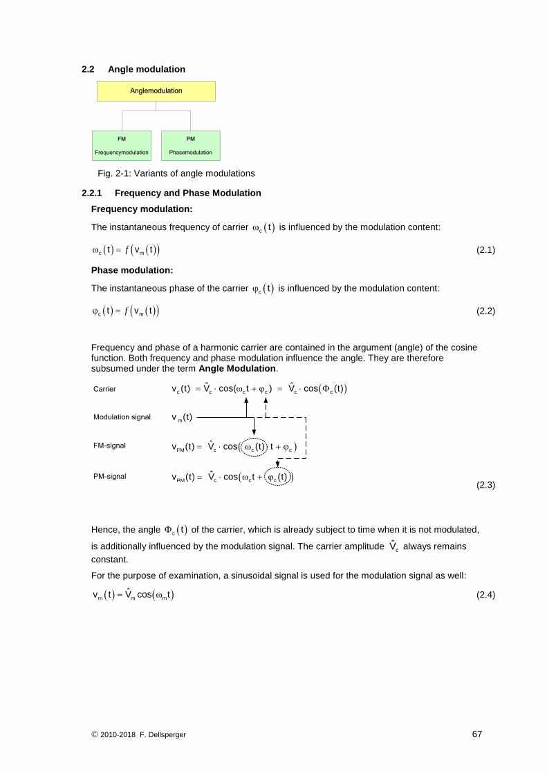
2.2 Angle modulation
Anglemodulation
FM
Frequencymodulation
PM
Phasemodulation
Fig. 2-1: Variants of angle modulations
2.2.1 Frequency and Phase Modulation
Frequency modulation:
The instantaneous frequency of carrier c t is influenced by the modulation content:
c mt v t f (2.1)
Phase modulation:
The instantaneous phase of the carrier c t is influenced by the modulation content:
c mt v t f (2.2)
Frequency and phase of a harmonic carrier are contained in the argument (angle) of the cosine function. Both frequency and phase modulation influence the angle. They are therefore subsumed under the term Angle Modulation.
c c c c c c
m
FM c c c
PM c c c
ˆ ˆv (t) V cos( t ) V cos (t)
v (t)
ˆv (t) V cos (t) t
ˆv (t) V cos t (t)
Carrier
Modulation signal
FM-signal
PM-signal
(2.3)
Hence, the angle c t of the carrier, which is already subject to time when it is not modulated,
is additionally influenced by the modulation signal. The carrier amplitude cV always remains
constant.
For the purpose of examination, a sinusoidal signal is used for the modulation signal as well:
m m mˆv t V cos t (2.4)
© 2010-2018 F. Dellsperger 68
The angle-modulated signal will be
PM c PMˆv t V cos t (2.5)
The entire instantaneous phase PM t is the sum of the carrier’s instantaneous phase
c ct t and the instantaneous phase m t , which is generated by the modulation signal.
PM c mt t t (2.6)
m c mt cos t (2.7)
In this case, c is the maximum phase difference between the modulated and the
unmodulated carrier. c is designated as phase deviation or modulation index .
PM c c mt t cos t (2.8)
Hence, the time function of the angle-modulated carrier will be
PM c c c m c c mˆ ˆv t V cos t cos t V cos t cos t (2.9)
From the instantaneous phase PM t , the instantaneous angular frequency of the modulated
carrier can be determined by way of differentiation:
PM
PM c c m m
d tt sin t
dt
(2.10)
The instantaneous frequency of the modulated carrier can be determined with c m c
PM
c c mPM t
tf f f sin t
2
(2.11)
The frequency deviation c c m mf f f is the maximum frequency difference between the
modulated and the unmodulated carrier.
For the modulation index , the following applies:
cc
m
f
f
(2.12)
From the equation (2.9) the time function of the frequency-modulated carrier can be described
cFM c c m
m
fˆv t V cos t cos tf
(2.13)
The equations (2.9) and (2.13) show that if the modulation frequency is constant, phase and frequency modulation cannot be distinguished.
Spectrum of Angle modulation
For the spectrum analysis, the Fourier coefficients must be determined. For this purpose, the equation (2.9) is represented as a complex equation:
c m c mj t cos( t) j t j cos( t)
PM c c m c cˆ ˆ ˆv (t) V cos t cos t V Re e V Re e e
(2.14)
© 2010-2018 F. Dellsperger 69
With the power series 2 3 n
x x x x xe 1
1! 2! 3! n! and mx j cos t ,
the factor mj cos( t )e can be represented as follows:
mj cos( t ) 2 2 2 3 3 3
m m m
2 2 3 3
m m m m
4 4
m m
1 1e 1 j cos( t) j cos ( t) j cos ( t)
2! 3!
1 1 1 11 j cos( t) j 1 cos(2 t) j cos(3 t) cos( t)
2! 2 3! 4
1 1j cos(3 t) 4cos(2 t) 3
4! 8
(2.15)
Sorted according to frequencies:
m
0
1
2 4 6
j cos( t )
J
3 5
m
J
2
1 1e 1 ...
2 4 2 36 2
1 12j ... cos( t)
2 2 2 12 2
12j
2 2
2
3
2 4 6
m
J
3 5 6
3
m
J
1 1... cos(2 t)
6 2 48 2
1 1 12j ... cos(3 t)
6 2 24 2 240 2
(2.16)
mj cos( t) 2 3
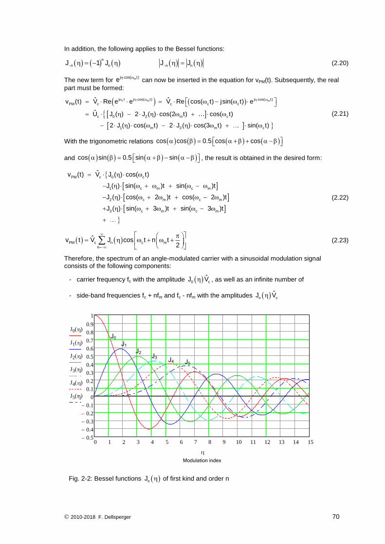
0 1 m 2 m 3 me J ( ) 2j J ( ) cos( t) 2j J ( ) cos(2 t) 2j J ( ) cos(3 t) (2.17)
Jn() are designated as Bessel functions of the first kind of order n (n = 0, 1, 2, 3, ...). Their function values can be found in diagrams or tables or they can be calculated numerically.
The following applies to the representation as a series:
n 2kk
nk 0
12
Jk! n k !
(2.18)
If the function values for n 0 and n 1 are known, the Bessel functions for n 2 can be
calculated iteratively:
n n 1 n 2
2 n 1J J J
(2.19)
© 2010-2018 F. Dellsperger 70
In addition, the following applies to the Bessel functions:
n
n n n nJ 1 J J J
(2.20)
The new term for mj cos( t )e can now be inserted in the equation for vPM(t). Subsequently, the real
part must be formed:
c m mj t j cos( t ) j cos( t )
PM c c c c
c 0 2 m c
1 m 3 m c
ˆ ˆv (t) V Re e e V Re cos( t) jsin( t) e
U J ( ) 2 J ( ) cos(2 t) cos( t)
2 J ( ) cos( t) 2 J ( ) cos(3 t) sin( t)
(2.21)
With the trigonometric relations cos cos 0.5 cos cos
and cos sin 0.5 sin sin , the result is obtained in the desired form:
PM c 0 c
1 c m c m
2 c m c m
3 c m c m
ˆv (t) V J ( ) cos( t)
J ( ) sin( )t sin( )t
J ( ) cos( 2 )t cos( 2 )t
J ( ) sin( 3 )t sin( 3 )t
(2.22)
PM c n c m
n
ˆv t V J cos t n t2
(2.23)
Therefore, the spectrum of an angle-modulated carrier with a sinusoidal modulation signal consists of the following components:
- carrier frequency fc with the amplitude 0 cˆJ V , as well as an infinite number of
- side-band frequencies fc + nfm and fc - nfm with the amplitudes n cˆJ V
0 1 2 3 4 5 6 7 8 9 10 11 12 13 14 150.5
0.4
0.3
0.2
0.1
0
0.1
0.2
0.3
0.4
0.5
0.6
0.7
0.8
0.9
1
Modulationindex
J0( )
J1( )
J2( )
J3( )
J4( )
J5( )
0
J0
J1
J2J3 J4 J5
Modulation index
Fig. 2-2: Bessel functions nJ of first kind and order n
© 2010-2018 F. Dellsperger 71
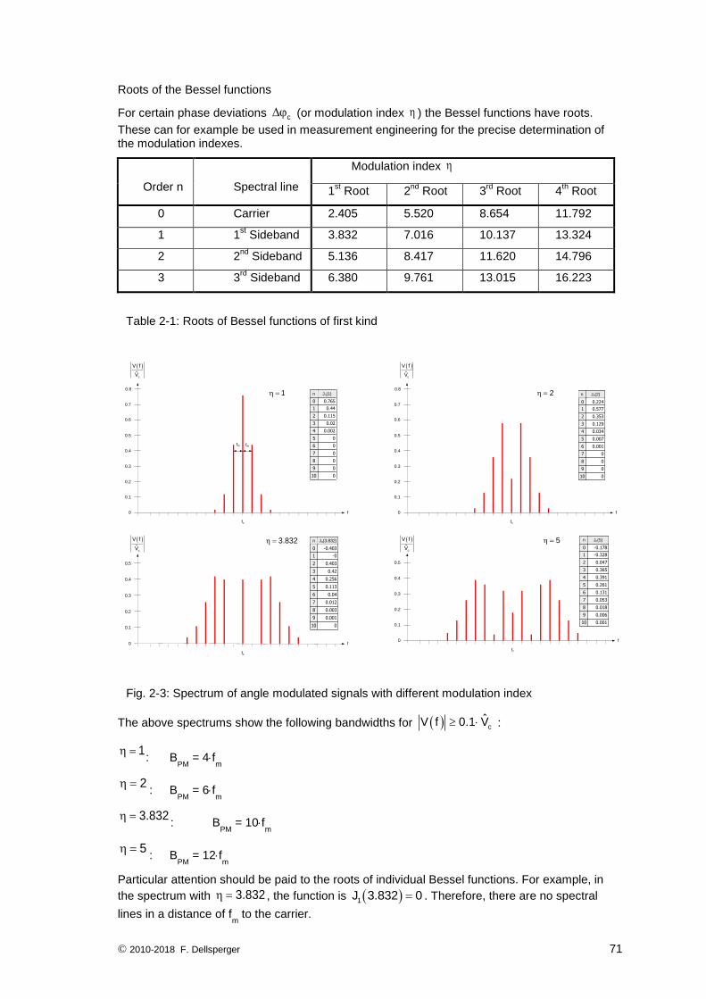
Roots of the Bessel functions
For certain phase deviations c (or modulation index ) the Bessel functions have roots.
These can for example be used in measurement engineering for the precise determination of the modulation indexes.
Order n
Spectral line
Modulation index
1st Root 2
nd Root 3
rd Root 4
th Root
0 Carrier 2.405 5.520 8.654 11.792
1 1st Sideband 3.832 7.016 10.137 13.324
2 2nd
Sideband 5.136 8.417 11.620 14.796
3 3rd
Sideband 6.380 9.761 13.015 16.223
Table 2-1: Roots of Bessel functions of first kind
0.1
0.2
0.3
0.4
0.5
0.6
0.7
0.8
0
fc
Jn
0
0
1
2
3
4
5
6
7
8
9
10
0.765
0.44
0.115
0.02
0.002
0
0
0
0
0
0
n Jn(1)
fmfm
1
c
V f
V
f
Jn
0
0
1
2
3
4
5
6
7
8
9
10
0.224
0.577
0.353
0.129
0.034
0.007
0.001
0
0
0
0
n Jn(2)
0.1
0.2
0.3
0.4
0.5
0.6
0.7
0.8
0
fc
2
c
V f
V
f
Jn
0
0
1
2
3
4
5
6
7
8
9
10
-0.403
-0
0.403
0.42
0.256
0.113
0.04
0.012
0.003
0.001
0
Jn(3.832)n
0.1
0.2
0.3
0.4
0.5
0
fc
3.832
c
V f
V
f
0.1
0.2
0.3
0.4
0.5
0
fc
5
c
V f
V
f
Jn
0
0
1
2
3
4
5
6
7
8
9
10
-0.178
-0.328
0.047
0.365
0.391
0.261
0.131
0.053
0.018
0.006
0.001
Jn(5)n
Fig. 2-3: Spectrum of angle modulated signals with different modulation index
The above spectrums show the following bandwidths for cˆV f 0.1 V :
1 : B
PM = 4f
m
2 : B
PM = 6f
m
3.832 : B
PM = 10f
m
5 : B
PM = 12f
m
Particular attention should be paid to the roots of individual Bessel functions. For example, in
the spectrum with 3.832 , the function is 1J 3.832 0 . Therefore, there are no spectral
lines in a distance of fm to the carrier.
© 2010-2018 F. Dellsperger 72
Bandwidth of the angle modulation
When we examine the above examples and the Bessel functions, it is noticeable that starting from a certain ordinal number n, the spectral lines become smaller and smaller, and soon reaches values close to zero. Due to this, the spectrum, which theoretically has an infinite width, is practically limited to a finite value.
If only spectral lines with amplitudes c
ˆ0.1 V are taken into account, the bandwidth of an angle
modulation signal can be represented as follows (Carson rule):
PM m mB 2 ( f f ) 2 f (1 ) (2.24)
If only spectral lines with amplitudes cˆ0.01 V are taken into account, the bandwidth will be:
PM m mB 2 ( f 2f ) 2 f ( 2) (2.25)
Another common definition for the bandwidth is the frequency range, which contains 99% of
the total power.
In the case of very small phase deviations of 0.3 , all values of the Bessel function with n>1
are smaller than 0.01 and the amplitude spectrum is hardly distinguishable from an AM signal. However, the phase spectrum shows a phase shift of -90° in the side frequencies. This case is often called narrow-band FM (NBFM):
NBFM: n0.3 J 0.01 for n 1 (2.26)
In contrast to this, an angle modulation with a large modulation index is called wide-band FM (WBFM).
A typical example for this is FM broadcasting with a maximum modulation frequency of 15 kHz
and a deviation stipulated in the standard of f 75kHz . Hence, the modulation index is
maxm
f 75kHz5
f 15kHz
and the bandwidth according to (2.24) is
FMB 2 15kHz 75kHz 180kHz
When the spectrum is calculated, there are 8 spectral lines with an amplitude of cˆ0.1V
on
each side of the carrier; thus, the bandwidth is FMB 2 8 15kHz 240kHz .
For AM, the relation between the bandwidth BAM and the modulation frequency fm is
AM
m
B2
f (2.27)
For the angle modulation, the relation is always greater than 2
PM
m
B2 1
f (2.28)
In the case of the angle modulation, the occupied bandwidth is always greater than with AM. It is subject to the modulation index .
© 2010-2018 F. Dellsperger 73
Power of angle modulation signals
As during angle modulation, the amplitude of the carrier is not changed, the total power just corresponds to the power of the unmodulated carrier.
2
cPM c
VP P
2 R
(2.29)
The amplitude of the spectral line of the carrier frequency fc is for modulated signals significantly smaller than the amplitude of an unmodulated carrier. Eventually however, all phasors of the spectrum are added to form the constant signal amplitude.
The sum of the powers of all spectral lines also equals the power PMP .
2
2cPM n
n
VP J
2 R
with 2
n
n
J 1
(2.30)
As angle-modulated signals have a constant amplitude, they can be amplified in a non-linear way without the generation of modulation distortions. This is a big advantage especially for high-power transmitters, because non-linear amplifiers can have a very high degree of efficiency.
Representation options for angle modulation
t
Tm
mV
mv t
Fig. 2-4: Modulation signal in time domain
Tm
f
t
cf f
cf f
cf
Fig. 2-5: Instantaneous frequency in time domain
© 2010-2018 F. Dellsperger 74
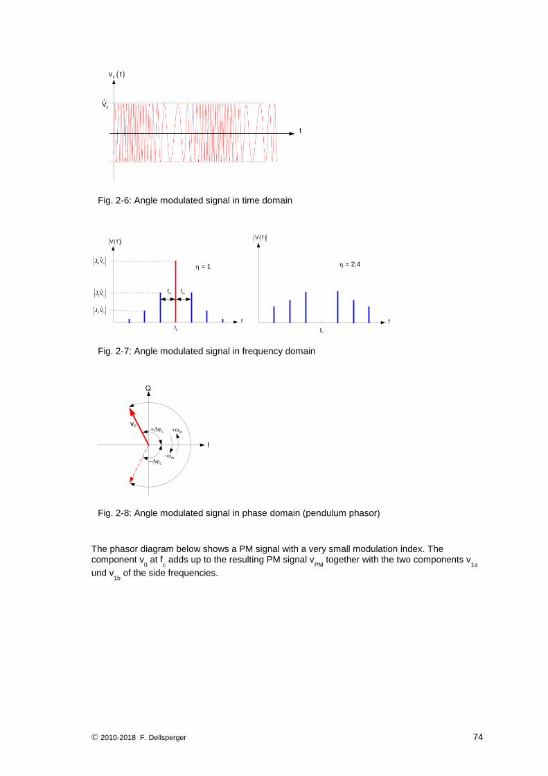
t
cV
cv t
Fig. 2-6: Angle modulated signal in time domain
fc
f
= 1
V f
mf mf
0 cˆJ V
1 cˆJ V
2 cˆJ V
fc
f
= 2.4
V f
Fig. 2-7: Angle modulated signal in frequency domain
I
Q
vc
c
cm
m
Fig. 2-8: Angle modulated signal in phase domain (pendulum phasor)
The phasor diagram below shows a PM signal with a very small modulation index. The component v
0 at f
c adds up to the resulting PM signal v
PM together with the two components v
1a
und v1b
of the side frequencies.
© 2010-2018 F. Dellsperger 75
v0
I
Q
v1b
v1a
vPM
c
m
m
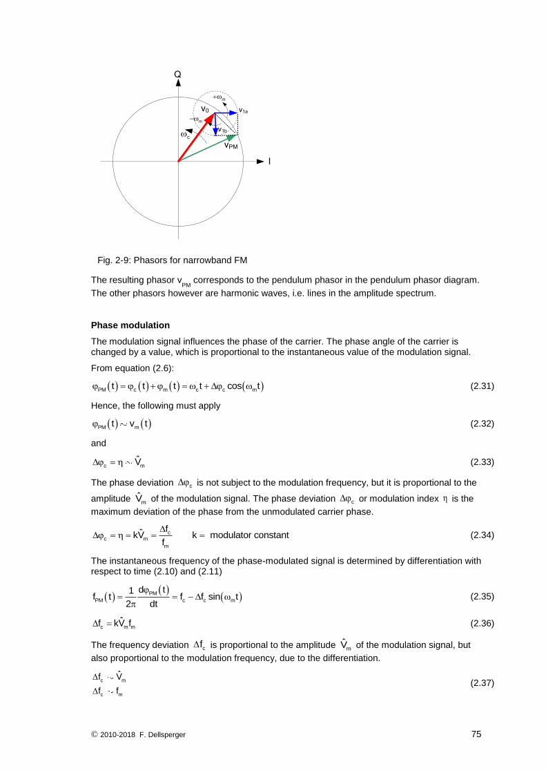
Fig. 2-9: Phasors for narrowband FM
The resulting phasor vPM
corresponds to the pendulum phasor in the pendulum phasor diagram.
The other phasors however are harmonic waves, i.e. lines in the amplitude spectrum.
Phase modulation
The modulation signal influences the phase of the carrier. The phase angle of the carrier is changed by a value, which is proportional to the instantaneous value of the modulation signal.
From equation (2.6):
PM c m c c mt t t t cos t (2.31)
Hence, the following must apply
PM mt v t (2.32)
and
c mV (2.33)
The phase deviation c is not subject to the modulation frequency, but it is proportional to the
amplitude mV of the modulation signal. The phase deviation c or modulation index is the
maximum deviation of the phase from the unmodulated carrier phase.
cc m
m
fˆkV k modulator constantf
(2.34)
The instantaneous frequency of the phase-modulated signal is determined by differentiation with respect to time (2.10) and (2.11)
PM
PM c c m
d t1f t f f sin t
2 dt
(2.35)
c m mˆf kV f (2.36)
The frequency deviation cf is proportional to the amplitude mV of the modulation signal, but
also proportional to the modulation frequency, due to the differentiation.
c m
c m
ˆf V
f f
(2.37)
© 2010-2018 F. Dellsperger 76
Frequency modulation
The modulation signal influences the frequency of the carrier. The frequency of the carrier is changed by a value, which is proportional to the instantaneous value of the modulation signal.
From equation (2.11):
c x c c m c m mFM tf f f t f f sin t f sin t (2.38)
Hence, the following must apply
x mf t v t (2.39)
and
c mˆf V (2.40)
The frequency deviation cf is not subject to the modulation frequency, but it is proportional to
the amplitude mV of the modulation signal. The frequency deviation cf is the maximum
deviation of the frequency from the unmodulated carrier frequency cf .
c m c mˆf kV f k modulator constant (2.41)
The instantaneous phase of the frequency-modulated signal is determined by means of integration with respect to time
FM FM c m
c mc m c m
m m
t t dt t k v t dt
ˆf kVt sin t t sin t
f f
(2.42)
mc
m
ˆkV
f (2.43)
The phase deviation c is proportional to the amplitude mV of the modulation signal, but also
inversely proportional to the modulation frequency.
c m
c
m
V
1
f
(2.44)
© 2010-2018 F. Dellsperger 77
0 1 2 31.5
1
0.5
0
0.5
1
1.5
vm t( )
t
ms
0 1 2 31.5
1
0.5
0
0.5
1
1.5
vPM t( )
t
ms
0 1 2 30
50
100
150
200
PM t( )
c t( )
t
ms
0 1 2 38
9
10
11
12
fPM t( )
kHz
fc t( )
kHz
t
ms
Modulation signal
Angle modulated signal
Phase transition
Frequency transition
Unmodulated carrier
Unmodulated carrier
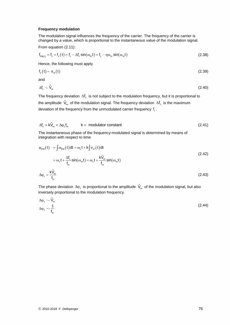
c mf 10 kHz f 500 Hz 2 ( f 1kHz)
Frequency deviation f
Phase deviation
(magnified by 10)
Fig. 2-10: Angle modulation with sinusoidal modulation signal
Fig. 2-11 shows a “Pendulum phasor diagram“ with the instantaneous position of the modulated
carrier phasor with respect to the unmodulated carrier (o0 "I" ).
The phase deviation c corresponds to the maximum deflection of the pendular phasor. The
frequency deviation cf is contained in the maximum oscillating speed max and max
.
© 2010-2018 F. Dellsperger 78
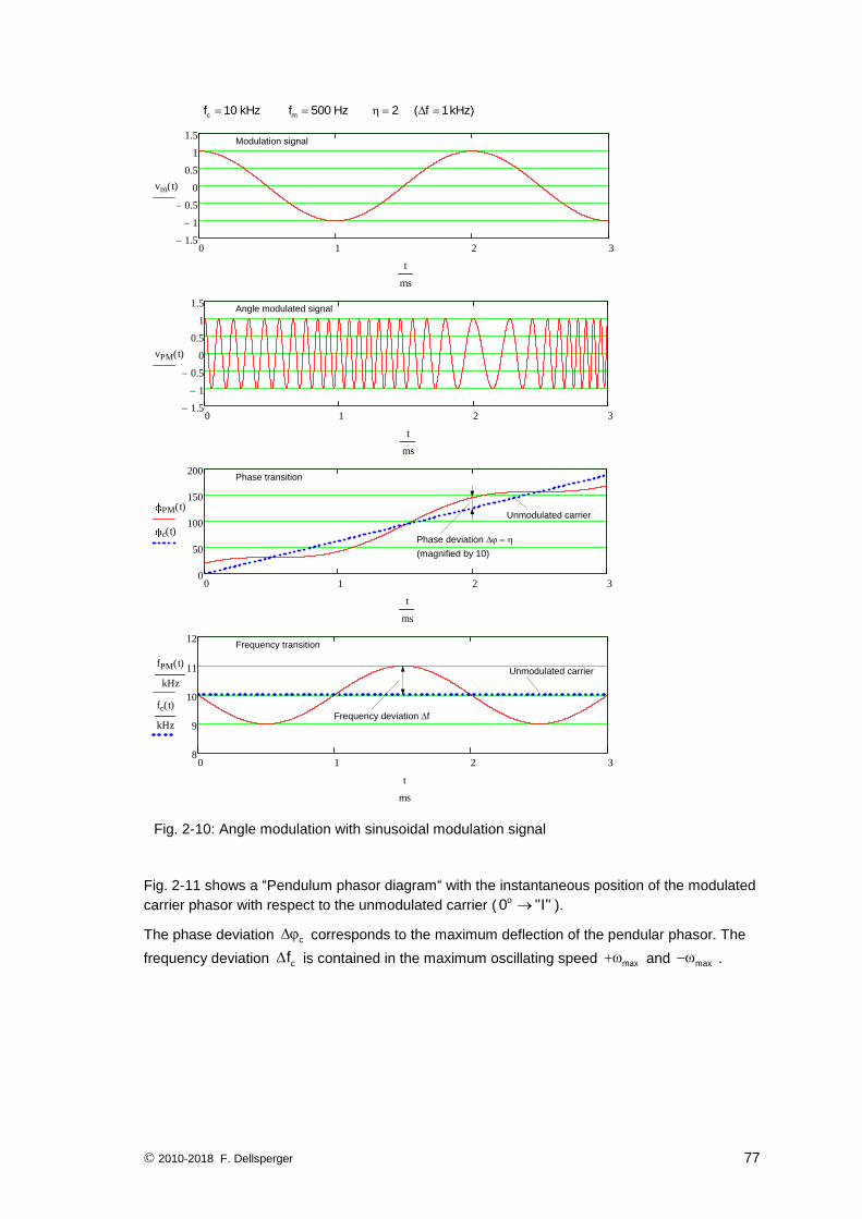
For a constant modulation frequency mf , the frequency deviation cf and the phase deviation
c or rather the modulation index are closely linked to one another:
cc m c
m
ff f bzw.
f
(2.45)
I
Q
cvc
c
Fig. 2-11: Pendulum phasor of a phase modulated signal
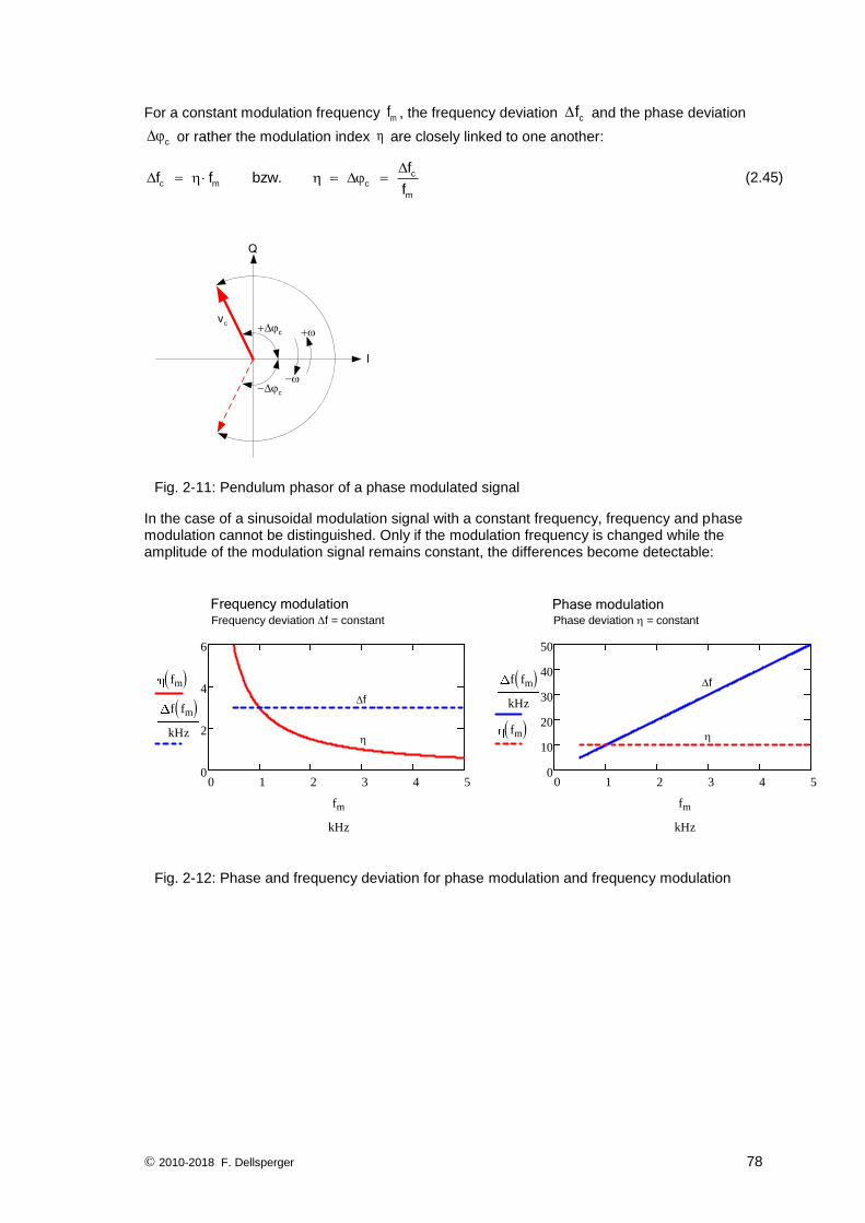
In the case of a sinusoidal modulation signal with a constant frequency, frequency and phase modulation cannot be distinguished. Only if the modulation frequency is changed while the amplitude of the modulation signal remains constant, the differences become detectable:
0 1 2 3 4 50
2
4
6
fm
f fm kHz
fm
kHz
0 1 2 3 4 50
10
20
30
40
50
f fm kHz
fm
fm
kHz
f
f
Frequency modulation Phase modulationFrequency deviation f = constant Phase deviation = constant
Fig. 2-12: Phase and frequency deviation for phase modulation and frequency modulation
© 2010-2018 F. Dellsperger 79
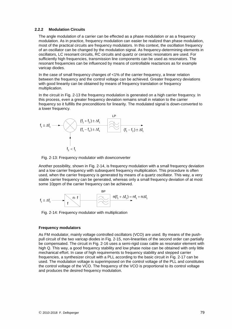
2.2.2 Modulation Circuits
The angle modulation of a carrier can be effected as a phase modulation or as a frequency modulation. As in practice, frequency modulation can easier be realized than phase modulation, most of the practical circuits are frequency modulators. In this context, the oscillation frequency of an oscillator can be changed by the modulation signal. As frequency-determining elements in oscillators, LC resonant circuits, RC circuits and quartz or ceramic resonators are used. For sufficiently high frequencies, transmission line components can be used as resonators. The resonant frequencies can be influenced by means of controllable reactances as for example varicap diodes.
In the case of small frequency changes of <1% of the carrier frequency, a linear relation between the frequency and the control voltage can be achieved. Greater frequency deviations with good linearity can be obtained by means of frequency translation or frequency multiplication.
In the circuit in Fig. 2-13 the frequency modulation is generated on a high carrier frequency. In this process, even a greater frequency deviation remains small in relation to the carrier frequency so it fulfills the preconditions for linearity. The modulated signal is down-converted to a lower frequency.
LP
1 1f f
2 1f f
1 2 1(f f ) f
1 2 1(f f ) f 1 2 1(f f ) f
Fig. 2-13: Frequency modulator with downconverter
Another possibility, shown in Fig. 2-14, is frequency modulation with a small frequency deviation and a low carrier frequency with subsequent frequency multiplication. This procedure is often used, when the carrier frequency is generated by means of a quartz oscillator. This way, a very stable carrier frequency can be generated, whereas only a small frequency deviation of at most some 10ppm of the carrier frequency can be achieved.
BP
f
n f1 1f f
1 1 1 1n(f f ) nf n f
Fig. 2-14: Frequency modulator with multiplication
Frequency modulators
As FM modulator, mainly voltage controlled oscillators (VCO) are used. By means of the push-pull circuit of the two varicap diodes in Fig. 2-15, non-linearities of the second order can partially be compensated. The circuit in Fig. 2-16 uses a semi-rigid coax cable as resonator element with high Q. This way, a good frequency stability and low phase noise can be obtained with only little mechanical effort. In case of high requirements to frequency stability and stepped carrier frequencies, a synthesizer circuit with a PLL according to the basic circuit in Fig. 2-17 can be used. The modulation voltage is superimposed on the control voltage of the PLL and constitutes the control voltage of the VCO. The frequency of the VCO is proportional to its control voltage and produces the desired frequency modulation.
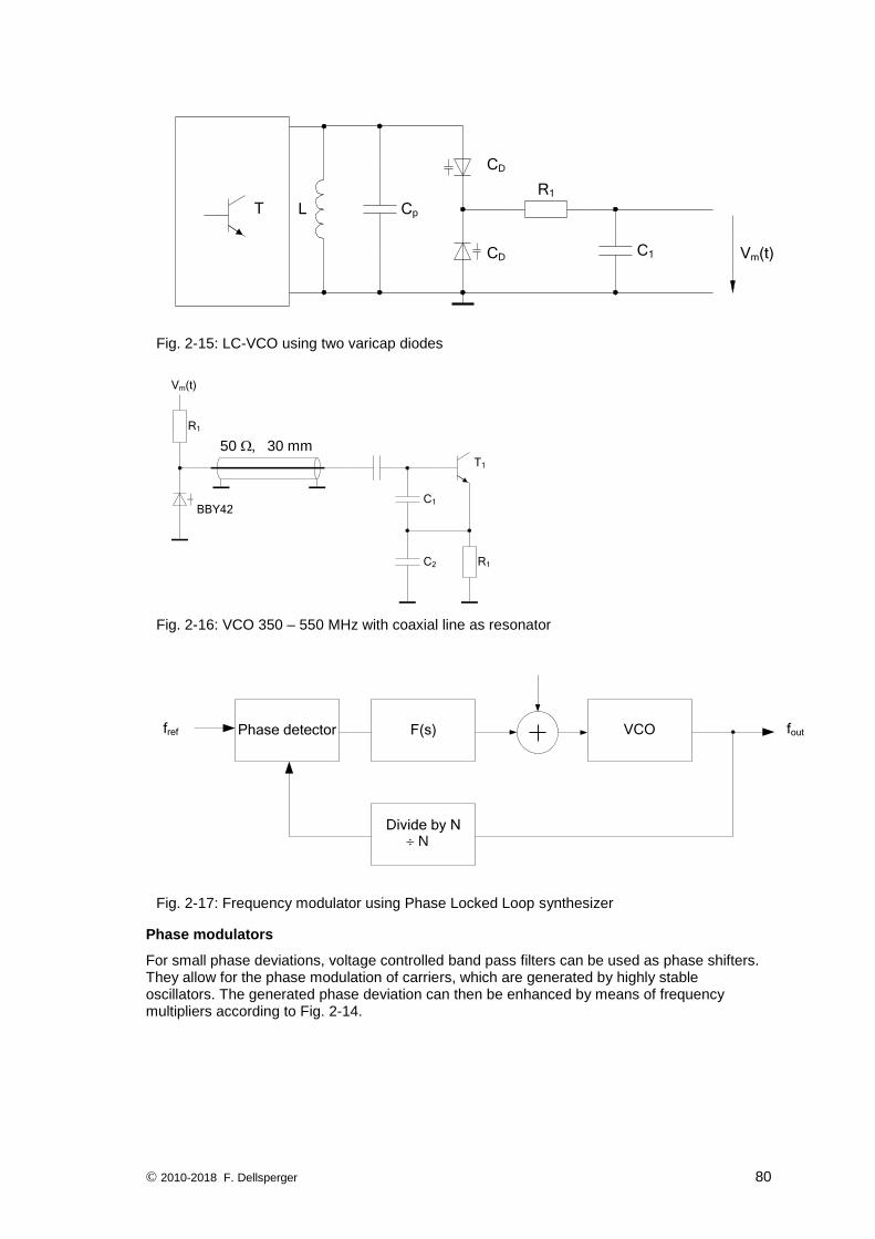
© 2010-2018 F. Dellsperger 80
L Cp
CD
R1
C1 Vm(t)
CD
T
Fig. 2-15: LC-VCO using two varicap diodes
T1
C1
C2 R1
BBY42
R1
50 , 30 mm
Vm(t)
Fig. 2-16: VCO 350 – 550 MHz with coaxial line as resonator
Phase detector F(s) VCO
Divide by N
fref fout
N
Fig. 2-17: Frequency modulator using Phase Locked Loop synthesizer
Phase modulators
For small phase deviations, voltage controlled band pass filters can be used as phase shifters. They allow for the phase modulation of carriers, which are generated by highly stable oscillators. The generated phase deviation can then be enhanced by means of frequency multipliers according to Fig. 2-14.
© 2010-2018 F. Dellsperger 81
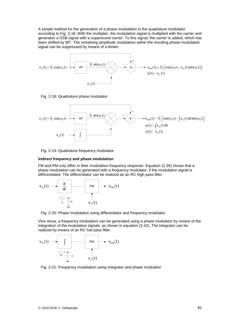
A simple method for the generation of a phase modulation is the quadrature modulator according to Fig. 2-18. With the multiplier, the modulation signal is multiplied with the carrier and generates a DSB signal with a suppressed carrier. To this signal, the carrier is added, which has been shifted by 90°. The remaining amplitude modulation within the resulting phase-modulated signal can be suppressed by means of a limiter.
c c cˆv t V cos t
mv t
-90o
PM c c m c
m
ˆv t V cos t v t sin t
t v t
c cV sin t
Fig. 2-18: Quadrature phase modulator
c c cˆv t V cos t
mv t
-90o
FM c c m c
m
m
ˆv t V cos t v t dt sin t
t v t dt
t v t
c cV sin t
Fig. 2-19: Quadrature frequency modulator
Indirect frequency and phase modulation
FM and PM only differ in their modulation frequency response. Equation (2.35) shows that a phase modulation can be generated with a frequency modulator, if the modulation signal is differentiated. The differentiator can be realized as an RC high pass filter.
FM PMv t
cv t
d
dt mv t
CR
Fig. 2-20: Phase modulation using differentiator and frequency modulator
Vice versa, a frequency modulation can be generated using a phase modulator by means of the integration of the modulation signals, as shown in equation (2.42). The integrator can be realized by means of an RC low pass filter.
PM FMv t
cv t
mv t
CR
Fig. 2-21: Frequency modulation using integrator and phase modulator
© 2010-2018 F. Dellsperger 82
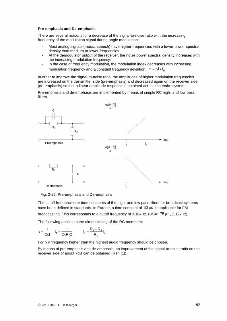
Pre-emphasis and De-emphasis
There are several reasons for a decrease of the signal-to-noise ratio with the increasing frequency of the modulation signal during angle modulation:
- Most analog signals (music, speech) have higher frequencies with a lower power spectral density than medium or lower frequencies.
- At the demodulator output of the receiver, the noise power spectral density increases with the increasing modulation frequency.
- In the case of frequency modulation, the modulation index decreases with increasing
modulation frequency and a constant frequency deviation. mf / f
In order to improve the signal-to-noise ratio, the amplitudes of higher modulation frequencies are increased on the transmitter side (pre-emphasis) and decreased again on the receiver side (de-emphasis) so that a linear amplitude response is obtained across the entire system.
Pre-emphasis and de-emphasis are implemented by means of simple RC high- and low pass filters.
R1
C
R2
log H f
log f
1f 2f
R1
C
log H f
log f
1f
Preemphasis
Deemphasis
Fig. 2-22: Pre-emphasis and De-emphasis
The cutoff frequencies or time constants of the high- and low pass filters for broadcast systems
have been defined in standards. In Europe, a time constant of 50 s is applicable for FM
broadcasting. This corresponds to a cutoff frequency of 3.18kHz. (USA: 75 s , 2.12kHz).
The following applies to the dimensioning of the RC members:
1
2 f
1
1
1f
2 R C
1 2
2 12
R Rf f
R
For f2 a frequency higher than the highest audio frequency should be chosen.
By means of pre-emphasis and de-emphasis, an improvement of the signal-to-noise ratio on the receiver side of about 7dB can be obtained (Ref. [1]).
© 2010-2018 F. Dellsperger 83
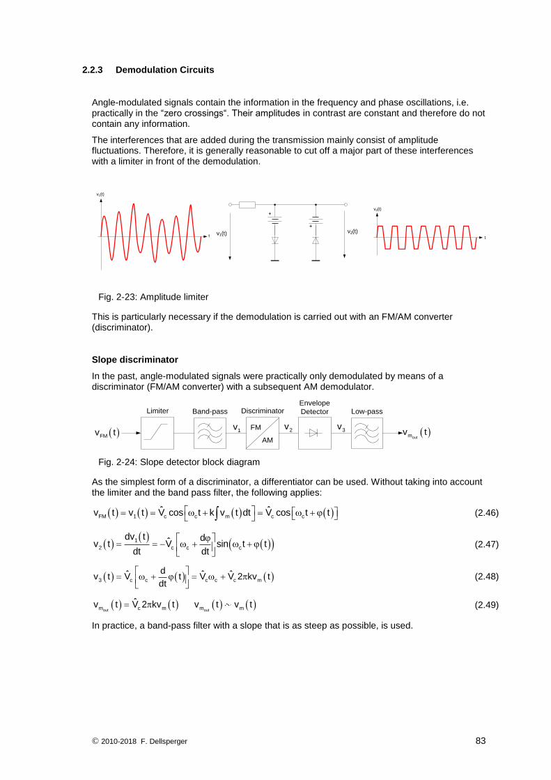
2.2.3 Demodulation Circuits
Angle-modulated signals contain the information in the frequency and phase oscillations, i.e. practically in the “zero crossings“. Their amplitudes in contrast are constant and therefore do not contain any information.
The interferences that are added during the transmission mainly consist of amplitude fluctuations. Therefore, it is generally reasonable to cut off a major part of these interferences with a limiter in front of the demodulation.
+
+
v1(t)v2(t)
v2(t)
tt
v1(t)
Fig. 2-23: Amplitude limiter
This is particularly necessary if the demodulation is carried out with an FM/AM converter (discriminator).
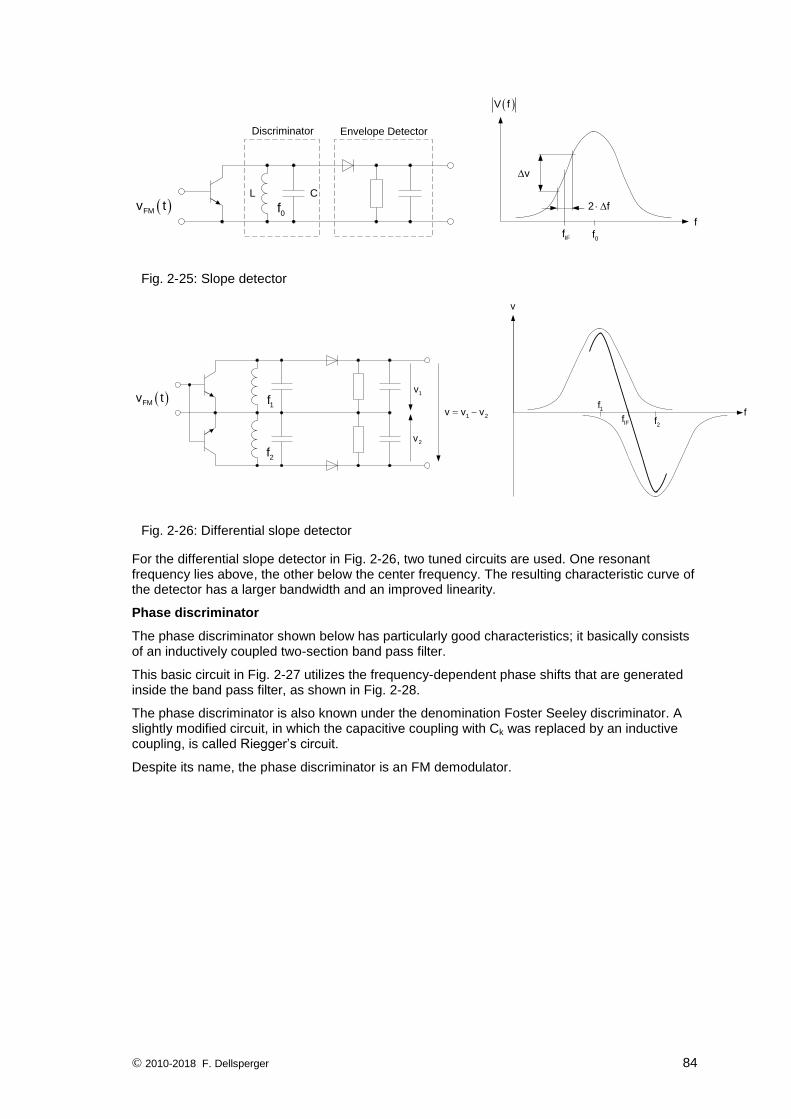
Slope discriminator
In the past, angle-modulated signals were practically only demodulated by means of a discriminator (FM/AM converter) with a subsequent AM demodulator.
Band-pass Low-pass
FMv t
Limiter
FM
AM
outmv t
DiscriminatorEnvelope
Detector
1v 2v 3v
Fig. 2-24: Slope detector block diagram
As the simplest form of a discriminator, a differentiator can be used. Without taking into account the limiter and the band pass filter, the following applies:
FM 1 c c m c cˆ ˆv t v t V cos t k v t dt V cos t t (2.46)
1
2 c c c
dv t dˆv t V sin t tdt dt
(2.47)
3 c c c c c m
dˆ ˆ ˆv t V t V V 2 kv tdt
(2.48)
out outm c m m m
ˆv t V 2 kv t v t v t (2.49)
In practice, a band-pass filter with a slope that is as steep as possible, is used.
© 2010-2018 F. Dellsperger 84
L C
0f
0fIFf
v
2 f
f
V f
FMv t
Discriminator Envelope Detector
Fig. 2-25: Slope detector
1f1f
IFff
v
FMv t
2f
2f
1v
2v
1 2v v v
Fig. 2-26: Differential slope detector
For the differential slope detector in Fig. 2-26, two tuned circuits are used. One resonant frequency lies above, the other below the center frequency. The resulting characteristic curve of the detector has a larger bandwidth and an improved linearity.
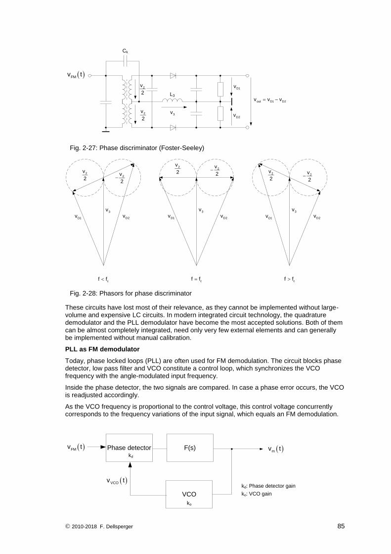
Phase discriminator
The phase discriminator shown below has particularly good characteristics; it basically consists of an inductively coupled two-section band pass filter.
This basic circuit in Fig. 2-27 utilizes the frequency-dependent phase shifts that are generated inside the band pass filter, as shown in Fig. 2-28.
The phase discriminator is also known under the denomination Foster Seeley discriminator. A slightly modified circuit, in which the capacitive coupling with Ck was replaced by an inductive coupling, is called Riegger’s circuit.
Despite its name, the phase discriminator is an FM demodulator.
© 2010-2018 F. Dellsperger 85
Ck
L3
FMv t
2v
2
2v
2
D1v
D2v
out D1 D2v v v
3v
Fig. 2-27: Phase discriminator (Foster-Seeley)
2v
22v
2
3v
D1v D2v
cf f
2v
22v
2
3v
D1v D2v
cf f
2v
22v
2
3v
D1v D2v
cf f
Fig. 2-28: Phasors for phase discriminator
These circuits have lost most of their relevance, as they cannot be implemented without large-volume and expensive LC circuits. In modern integrated circuit technology, the quadrature demodulator and the PLL demodulator have become the most accepted solutions. Both of them can be almost completely integrated, need only very few external elements and can generally be implemented without manual calibration.
PLL as FM demodulator
Today, phase locked loops (PLL) are often used for FM demodulation. The circuit blocks phase detector, low pass filter and VCO constitute a control loop, which synchronizes the VCO frequency with the angle-modulated input frequency.
Inside the phase detector, the two signals are compared. In case a phase error occurs, the VCO is readjusted accordingly.
As the VCO frequency is proportional to the control voltage, this control voltage concurrently corresponds to the frequency variations of the input signal, which equals an FM demodulation.
Phase detector F(s)
VCO
mv t FMv t
VCOv t
kd
ko
kd: Phase detector gain
ko: VCO gain
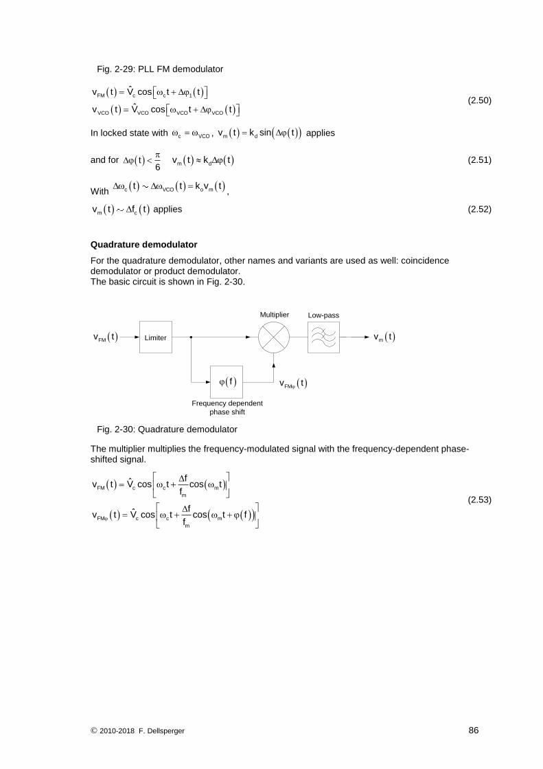
© 2010-2018 F. Dellsperger 86
Fig. 2-29: PLL FM demodulator
FM c c 1
VCO VCO VCO VCO
ˆv t V cos t t
ˆv t V cos t t
(2.50)
In locked state with c VCO , m dv t k sin t applies
and for t6
m dv t k t (2.51)
With c VCO o mt t k v t
,
m cv t f t applies (2.52)
Quadrature demodulator
For the quadrature demodulator, other names and variants are used as well: coincidence demodulator or product demodulator. The basic circuit is shown in Fig. 2-30.
FMv t mv t
f
Low-pass
FMv t
Frequency dependent
phase shift
Multiplier
Limiter
Fig. 2-30: Quadrature demodulator
The multiplier multiplies the frequency-modulated signal with the frequency-dependent phase-shifted signal.
FM c c m
m
FM c c m
m
fˆv t V cos t cos tf
fˆv t V cos t cos t ff
(2.53)
© 2010-2018 F. Dellsperger 87
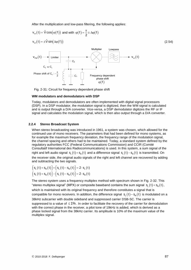
After the multiplication and low-pass filtering, the following applies:
mˆv t V cos f and with f f
2
mˆv t V sin f (2.54)
FMv t mv t
f
Lowpass
Frequency dependent
phase shift
Multiplier
Limiter
Ck
C1
k 1C C
kPhase shift of C :2
Fig. 2-31: Circuit for frequency dependent phase shift
WM modulators and demodulators with DSP
Today, modulators and demodulators are often implemented with digital signal processors (DSP). In a DSP modulator, the modulation signal is digitized, then the WM signal is calculated and is output through a D/A converter. Vice-versa, a DSP demodulator digitizes the RF or IF signal and calculates the modulation signal, which is then also output through a D/A converter.
2.2.4 Stereo Broadcast System
When stereo broadcasting was introduced in 1961, a system was chosen, which allowed for the continued use of mono receivers. The parameters that had been defined for mono systems, as for example the maximum frequency deviation, the frequency range of the modulation signal, the channel spacing and others had to be maintained. Today, a standard system defined by the regulatory authorities FCC (Federal Communications Commission) and CCIR (Comité Consultatif International des Radiocommunications) is used. In this system, a sum signal of the
right and left audio signal L Rs t s t and a difference signal L Rs t s t is transmitted. On
the receiver side, the original audio signals of the right and left channel are recovered by adding and subtracting the two signals.
L R L R L
L R L R R
s t s t s t s t 2 s t
s t s t s t s t 2 s t
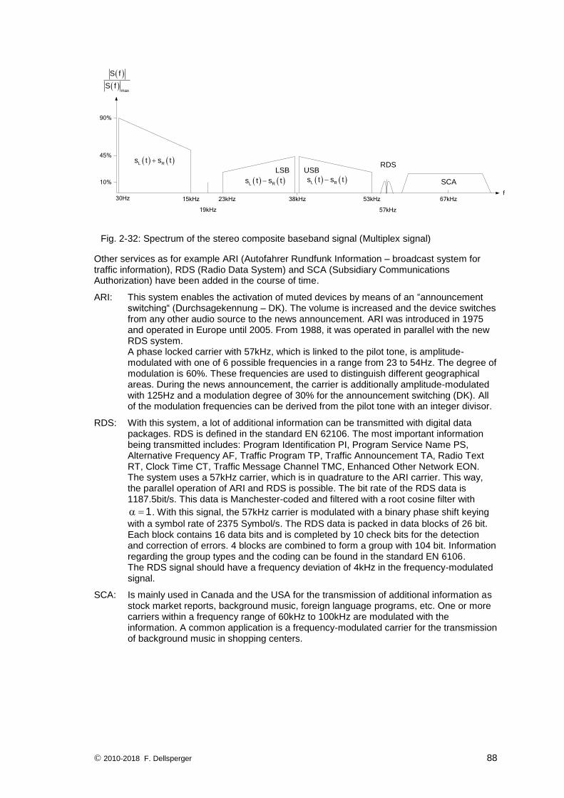
The stereo system uses a frequency multiplex method with spectrum shown in Fig. 2-32. This
“stereo multiplex signal” (MPX) or composite baseband contains the sum signal L Rs t s t ,
which is maintained with its original frequency and therefore constitutes a signal that is
compatible for mono receivers. In addition, the difference signal L Rs t s t is modulated on a
38kHz subcarrier with double sideband and suppressed carrier DSB-SC. The carrier is
suppressed to a value of 1% . In order to facilitate the recovery of the carrier for demodulation
with the correct phase in the receiver, a pilot tone of 19kHz is added, which is derived as a phase locked signal from the 38kHz carrier. Its amplitude is 10% of the maximum value of the multiplex signal.
© 2010-2018 F. Dellsperger 88
max
S f
S f
L Rs t s t
30Hz 15kHz
19kHz
23kHz 38kHz 53kHz 67kHz
10%
45%
90%
L Rs t s t
LSB USB
L Rs t s t SCA
RDS
f
57kHz
Fig. 2-32: Spectrum of the stereo composite baseband signal (Multiplex signal)
Other services as for example ARI (Autofahrer Rundfunk Information – broadcast system for traffic information), RDS (Radio Data System) and SCA (Subsidiary Communications Authorization) have been added in the course of time.
ARI: This system enables the activation of muted devices by means of an “announcement switching“ (Durchsagekennung – DK). The volume is increased and the device switches from any other audio source to the news announcement. ARI was introduced in 1975 and operated in Europe until 2005. From 1988, it was operated in parallel with the new RDS system. A phase locked carrier with 57kHz, which is linked to the pilot tone, is amplitude-modulated with one of 6 possible frequencies in a range from 23 to 54Hz. The degree of modulation is 60%. These frequencies are used to distinguish different geographical areas. During the news announcement, the carrier is additionally amplitude-modulated with 125Hz and a modulation degree of 30% for the announcement switching (DK). All of the modulation frequencies can be derived from the pilot tone with an integer divisor.
RDS: With this system, a lot of additional information can be transmitted with digital data packages. RDS is defined in the standard EN 62106. The most important information being transmitted includes: Program Identification PI, Program Service Name PS, Alternative Frequency AF, Traffic Program TP, Traffic Announcement TA, Radio Text RT, Clock Time CT, Traffic Message Channel TMC, Enhanced Other Network EON. The system uses a 57kHz carrier, which is in quadrature to the ARI carrier. This way, the parallel operation of ARI and RDS is possible. The bit rate of the RDS data is 1187.5bit/s. This data is Manchester-coded and filtered with a root cosine filter with
1 . With this signal, the 57kHz carrier is modulated with a binary phase shift keying
with a symbol rate of 2375 Symbol/s. The RDS data is packed in data blocks of 26 bit. Each block contains 16 data bits and is completed by 10 check bits for the detection and correction of errors. 4 blocks are combined to form a group with 104 bit. Information regarding the group types and the coding can be found in the standard EN 6106. The RDS signal should have a frequency deviation of 4kHz in the frequency-modulated signal.
SCA: Is mainly used in Canada and the USA for the transmission of additional information as stock market reports, background music, foreign language programs, etc. One or more carriers within a frequency range of 60kHz to 100kHz are modulated with the information. A common application is a frequency-modulated carrier for the transmission of background music in shopping centers.
© 2010-2018 F. Dellsperger 89
Preemphasis
2
Preemphasis
L Rs t s t
L Rs t s t
Left audio
channel
Pilot
19 kHz
RDS
57 kHz
MPXs t
Ls t
Rs t
Right audio
channel
38 kHz
DSB-SC
Fig. 2-33: Stereo coder block diagram
The complete baseband signal (MPX) is fed to the FM modulator of a transmitter. In order to limit the bandwidth of the modulated stereo signal, which could become too large due to the larger bandwidth of the baseband (57kHz without SCA in comparison to 15kHz with mono), the maximum frequency deviation for stereo was reduced from 75kHz to 67.5kHz. According to Carson (2.24), the bandwidth of the frequency-modulated stereo signal would then be
B 2 67.5 kHz 57 kHz 249 kHz
in comparison to 180 kHz with the mono signal.
Stereo Coder
Rs t
Ls t
FM Modulator
Composite
Baseband
MPXs t
Power AmplifierTX Output
Fig. 2-34: Stereo transmitter
In the receiver, the first step is to recover the multiplex signal by means of an FM demodulator. For decoding the stereo multiplex signal and recovering the left and right audio signals, there are different solutions.
FM
DemodulatorStereo Decoder
Rs t
Ls t
Composite
Baseband
MPXs t
FM Receiver
Fig. 2-35: Stereo receiver
Matrix decoder:
The sum signal L Rs t s t is recovered by means of a low pass with a cut-off frequency of
15kHz. By means of a band pass filter from 23 to 53kHz, the DSB signal is recovered and demodulated in a synchronous demodulator by multiplication with the reconstructed carrier.
After 15kHz low pass filtering, the difference signal L Rs t s t is available. By adding and
subtracting inside a resistor matrix network, the left and right audio signal is recovered.
The 38kHz carrier can be recovered by doubling the frequency of the pilot tone or by means of a PLL circuit.
© 2010-2018 F. Dellsperger 90
BP 19 kHz
BP 23 – 53 kHz
LP 15 kHz
From FM-Demod
MPXs t
L Rs t s t
Freq. Doubler
19 kHz
38 kHz
LP 15 kHz
L Rs t s t
L2 s t
R2 s t
Fig. 2-36: Matrix stereo decoder
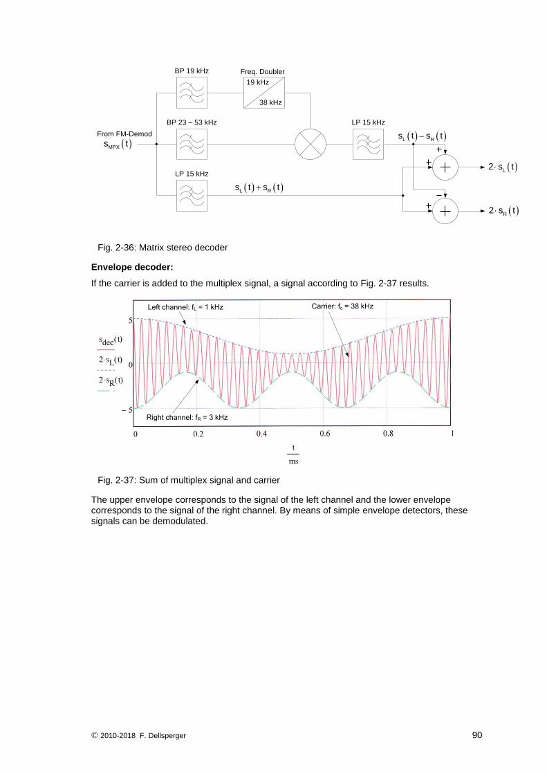
Envelope decoder:
If the carrier is added to the multiplex signal, a signal according to Fig. 2-37 results.
Left channel: fL = 1 kHz Carrier: fc = 38 kHz
Right channel: fR = 3 kHz
Fig. 2-37: Sum of multiplex signal and carrier
The upper envelope corresponds to the signal of the left channel and the lower envelope corresponds to the signal of the right channel. By means of simple envelope detectors, these signals can be demodulated.
© 2010-2018 F. Dellsperger 91
BP 19 kHz
LP 53 kHz
From FM-Demod
MPXs t
Freq. Doubler
19 kHz
38 kHz
L2 s t
R2 s t
BS 19 kHz
LP 15 kHz
LP 15 kHz
Fig. 2-38: Envelope-decoder
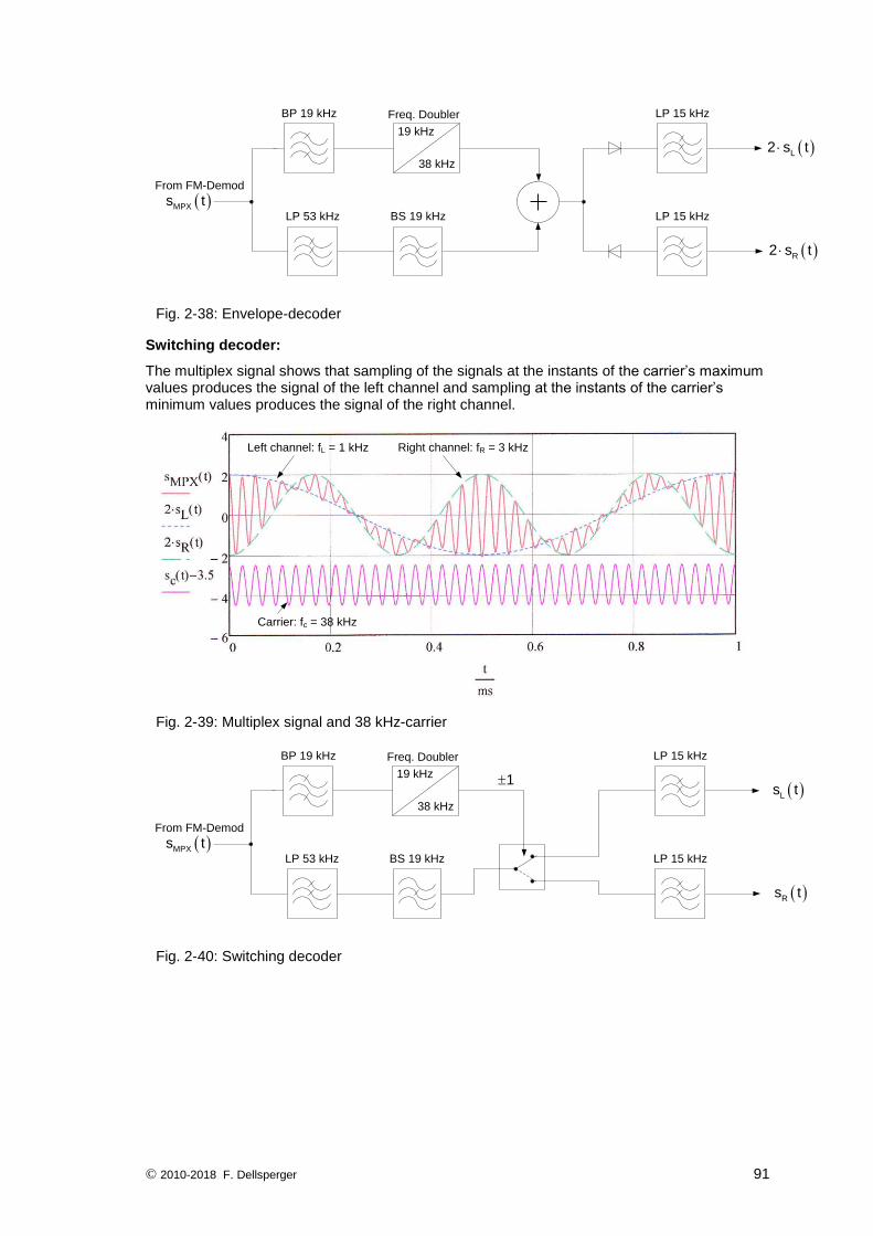
Switching decoder:
The multiplex signal shows that sampling of the signals at the instants of the carrier’s maximum values produces the signal of the left channel and sampling at the instants of the carrier’s minimum values produces the signal of the right channel.
Left channel: fL = 1 kHz Right channel: fR = 3 kHz
Carrier: fc = 38 kHz
Fig. 2-39: Multiplex signal and 38 kHz-carrier
BP 19 kHz
LP 53 kHz
From FM-Demod
MPXs t
Freq. Doubler
19 kHz
38 kHz
Ls t
Rs t
BS 19 kHz
LP 15 kHz
LP 15 kHz
1
Fig. 2-40: Switching decoder
© 2010-2018 F. Dellsperger 92
2.2.5 Distortion and noise behavior of FM
Distortions due to bandwidth limitation
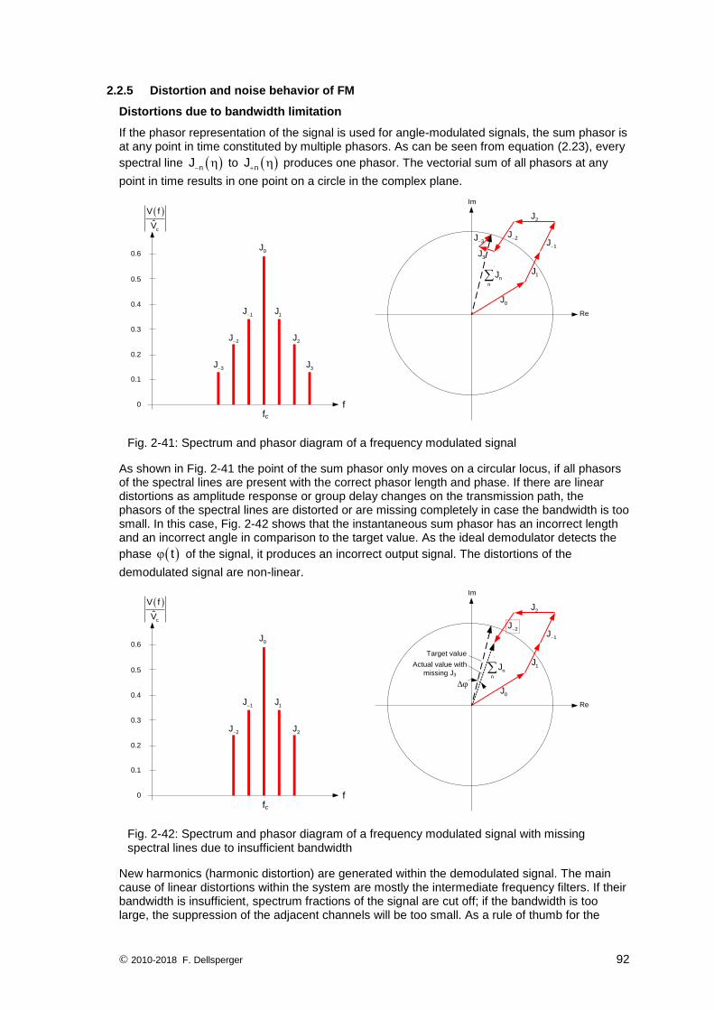
If the phasor representation of the signal is used for angle-modulated signals, the sum phasor is at any point in time constituted by multiple phasors. As can be seen from equation (2.23), every
spectral line nJ
to nJ
produces one phasor. The vectorial sum of all phasors at any
point in time results in one point on a circle in the complex plane.
fc
Im
Re
0J
1J
1J
2J
3J
3J
2J
n
n
J
0J
1J
1J
2J
3J 3
J
2J
f
0.1
0.2
0.3
0.4
0.5
0.6
0
c
V f
V
Fig. 2-41: Spectrum and phasor diagram of a frequency modulated signal
As shown in Fig. 2-41 the point of the sum phasor only moves on a circular locus, if all phasors of the spectral lines are present with the correct phasor length and phase. If there are linear distortions as amplitude response or group delay changes on the transmission path, the phasors of the spectral lines are distorted or are missing completely in case the bandwidth is too small. In this case, Fig. 2-42 shows that the instantaneous sum phasor has an incorrect length and an incorrect angle in comparison to the target value. As the ideal demodulator detects the
phase t of the signal, it produces an incorrect output signal. The distortions of the
demodulated signal are non-linear.
Im
Re
Target value
Actual value with
missing J3
0J
1J
1J
2J
2J
n
n
J
fc
0J
1J
1J
2J
2J
f
0.1
0.2
0.3
0.4
0.5
0.6
0
c
V f
V
Fig. 2-42: Spectrum and phasor diagram of a frequency modulated signal with missing spectral lines due to insufficient bandwidth
New harmonics (harmonic distortion) are generated within the demodulated signal. The main cause of linear distortions within the system are mostly the intermediate frequency filters. If their bandwidth is insufficient, spectrum fractions of the signal are cut off; if the bandwidth is too large, the suppression of the adjacent channels will be too small. As a rule of thumb for the
© 2010-2018 F. Dellsperger 93
necessary bandwidth for a required distortion factor of the demodulated signal, the following applies:
max
max
m
m
THD 10% : B 2 f f (Carson Rule)
THD 1% : B 2 f 2f
see also (2.24) and (2.25) (2.55)
Here, the distortions of the demodulator have not been taken into account.
Noise
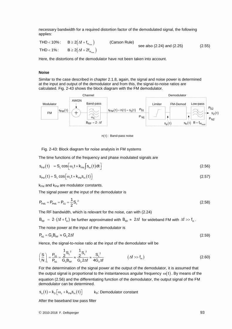
Similar to the case described in chapter 2.1.8, again, the signal and noise power is determined at the input and output of the demodulator and from this, the signal-to-noise ratios are calculated. Fig. 2-43 shows the block diagram with the FM demodulator.
Band-pass Low-passModulator Limiter
Demodulator
AWGN
maxmB f
Channel
c
S1P S2P
N1PN2P
FMs t FM 1s t n t s t
n t : Band-pass noise
FM
FM-Demod
as t bs t
2s t
RFB 2 f
Fig. 2-43: Block diagram for noise analysis in FM systems
The time functions of the frequency and phase modulated signals are
FM c c FM ms t S cos t k s t dt (2.56)
PM c c PM ms t S cos t k s t (2.57)
kFM and kPM are modulator constants.
The signal power at the input of the demodulator is
2
FM1 PM1 S1 c
1P P P S
2 (2.58)
The RF bandwidth, which is relevant for the noise, can with (2.24)
RF mB 2 ( f f ) be further approximated with RFB 2 f for wideband FM with mf f .
The noise power at the input of the demodulator is
N1 o RF oP G B G 2 f (2.59)
Hence, the signal-to-noise ratio at the input of the demodulator will be
2 22c c
S1 c
1 N1 o RF o o
1 1S S
P SS 2 2
N P G B G 2 f 4G f
mf f (2.60)
For the determination of the signal power at the output of the demodulator, it is assumed that
the output signal is proportional to the instantaneous angular frequency t . By means of the
equation (2.56) and the differentiating function of the demodulator, the output signal of the FM demodulator can be determined.
a D c FM ms t k k s t kD: Demodulator constant
After the baseband low pass filter
© 2010-2018 F. Dellsperger 94
a D FM ms t k k s t (2.61)
Accordingly, the signal power at the output
2 2 2
S2 D FM mP k k s t (2.62)
For the calculation of the noise power at the output, an unmodulated ms t 0 carrier and the
additive noise are analyzed. It can be demonstrated that the noise is approximately independent
of ms t . For the purpose of noise analysis, the signal at the input of the demodulator is
1 c c I c Q c
I c Q c
s t Scos t n t Scos t n t cos t n t sin t
S n t cos t n t sin t
(2.63)
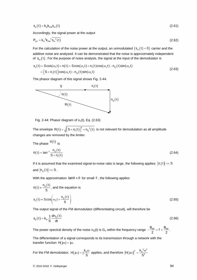
The phasor diagram of this signal shows Fig. 2-44.
t
S In t
R t
Qn t
Fig. 2-44: Phasor diagram of s1(t), Eq. (2.63)
The envelope 2 2
I QR t S n t n t is not relevant for demodulation as all amplitude
changes are removed by the limiter.
The phase t
is
Q1
I
n tt tan
S n t
(2.64)
If it is assumed that the examined signal-to-noise ratio is large, the following applies: in t S
and Qn t S .
With the approximation tan for small , the following applies
Qn t
tS
, and the equation is
Q
1 c
n ts t Scos t
S
(2.65)
The output signal of the FM demodulator (differentiating circuit), will therefore be
Q
b D
dn t1s t k
S dt (2.66)
The power spectral density of the noise nQ(t) is Go within the frequency range RF RFB Bf
2 2 .
The differentiation of a signal corresponds to its transmission through a network with the
transfer function H j j .
For the FM demodulator, DkH j j
S
applies, and therefore
2 22
D
2
kH j
S
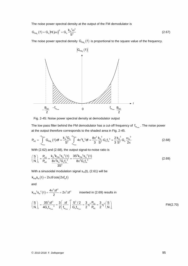
© 2010-2018 F. Dellsperger 95
The noise power spectral density at the output of the FM demodulator is
b
2 22
DFM o o 2
kG f G H j G
S
(2.67)
The noise power spectral density bFMG f is proportional to the square value of the frequency.
f
bFM
G f
maxmf
maxmf
0RFB
2 RF
B
2
Fig. 2-45: Noise power spectral density at demodulator output
The low pass filter behind the FM demodulator has a cut-off frequency of maxmf . The noise power
at the output therefore corresponds to the shaded area in Fig. 2-45.
m mmax max
b
m mmax max
f f2 2 2 322 2 3d o D D m
N2 FM m o m o2 2 2
f f
k G k k8 2P G f df 4 f df G f G
3 3 2S S S
(2.68)
With (2.62) and (2.68), the output signal-to-noise ratio is
2 2 2 2 2 2
D FM m FM mS2
2 2 3 2 3
2 N2 D o m o m
2
k k s t 3S k s tPS
N P 8 k G f 8 G f
3S
(2.69)
With a sinusoidal modulation signal sm(t), (2.61) will be
FM m mk s t 2 f cos 2 f t
and
2 2
2 2 2 2
FM m
4 fk s t 2 f
2
inserted in (2.69) results in
max maxmax
22 2 2
2 2S1
3
2 1m o m N1o m
PS 3S f 3 f S / 2 3 3 S
N 2 f G f 2 P 2 N4G f
FM (2.70)
© 2010-2018 F. Dellsperger 96
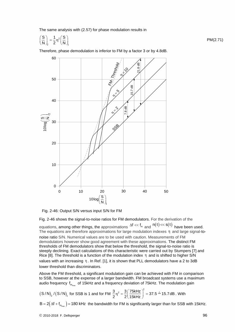
The same analysis with (2.57) for phase modulation results in
2
2 1
S 1 S
N 2 N
PM (2.71)
Therefore, phase demodulation is inferior to FM by a factor 3 or by 4.8dB.
0 10 20 30 40
0
10
20
30
40
50
60
2
S1
0lo
gN
1
S10log
N
2
5
10
SSB
50
FM
- T
hre
shold
7.8
dB
15
.7 d
B
21.8
dB
Fig. 2-46: Output S/N versus input S/N for FM
Fig. 2-46 shows the signal-to-noise ratios for FM demodulators. For the derivation of the
equations, among other things, the approximations mf f and
n t s t have been used.
The equations are therefore approximations for large modulation indexes and large signal-to-
noise ratio S/N. Numerical values are to be used with caution. Measurements of FM demodulators however show good agreement with these approximations. The distinct FM thresholds of FM demodulators show that below the threshold, the signal-to-noise ratio is steeply declining. Exact calculations of this characteristic were carried out by Stumpers [7] and Rice [8]. The threshold is a function of the modulation index and is shifted to higher S/N
values with an increasing . In Ref. [1], it is shown that PLL demodulators have a 2 to 3dB
lower threshold than discriminators.
Above the FM threshold, a significant modulation gain can be achieved with FM in comparison to SSB, however at the expense of a larger bandwidth. FM broadcast systems use a maximum
audio frequency maxmf of 15kHz and a frequency deviation of 75kHz. The modulation gain
2 1
S / N / S / N for SSB is 1 and for FM
2
23 3 75kHz37.5 15.7dB
2 2 15kHz
. With
maxmB 2 f f 180 kHz the bandwidth for FM is significantly larger than for SSB with 15kHz.
© 2010-2018 F. Dellsperger 97
Below the FM threshold, the modulation gain rapidly declines and is even smaller for small S/N than for SSB.
Above the FM threshold, FM is superior to SSB with a modulation index of 2
0.823
.
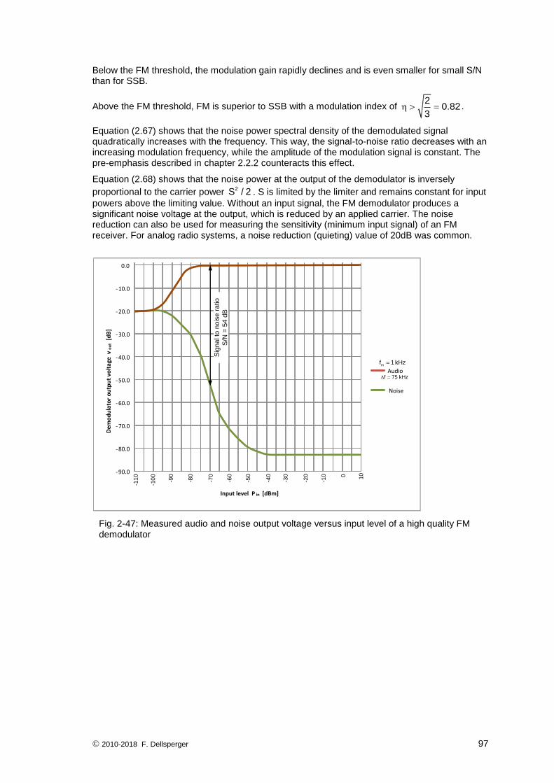
Equation (2.67) shows that the noise power spectral density of the demodulated signal quadratically increases with the frequency. This way, the signal-to-noise ratio decreases with an increasing modulation frequency, while the amplitude of the modulation signal is constant. The pre-emphasis described in chapter 2.2.2 counteracts this effect.
Equation (2.68) shows that the noise power at the output of the demodulator is inversely
proportional to the carrier power 2S / 2 . S is limited by the limiter and remains constant for input
powers above the limiting value. Without an input signal, the FM demodulator produces a significant noise voltage at the output, which is reduced by an applied carrier. The noise reduction can also be used for measuring the sensitivity (minimum input signal) of an FM receiver. For analog radio systems, a noise reduction (quieting) value of 20dB was common.
-90.0
-80.0
-70.0
-60.0
-50.0
-40.0
-30.0
-20.0
-10.0
0.0
Input level P in [dBm]
Audio
NoiseDeem:OFF
mf 1kHz
f 75 kHz
Sig
na
l to
no
ise
ra
tio
S/N
= 5
4 d
B
De
mo
du
lato
r o
utp
ut
volt
age
v
-11
0
-10
0
-90
-80
-70
-60
-50
-40
-30
-20
-10 0 10
ou
t[d
B]
Fig. 2-47: Measured audio and noise output voltage versus input level of a high quality FM demodulator
© 2010-2018 F. Dellsperger 98
2.3 References
[1] Taub, H., Schilling, D.L.: Principles of communication systems. McGraw-Hill, 2nd Edition 1986
[2] Kammeyer, K.D. : Nachrichtenübertragung. Vieweg+Teubner, 4. Auflage 2008
[3] Roppel, C.: Grundlagen der digitalen Kommunikationstechnik. Carl Hanser Verlag, 2006
[4] Ohm, J-R., Lüke, H.D.:Signalübertragung. Springer Verlag Berlin, 10. Auflage 2007
[5] Schwartz, M.: Information, Transmission, Modulation, and Noise. McGraw-Hill, 1980
[6] Zinke, O., Brunswig, H.: Hochfrequenztechnik 2, Springer Verlag Berlin, 5. Auflage 1999
[7] Stumpers, F.L.M.H.: Theory of frequency modulation noise. Proc. Inst. Radio Engrs. 36, 1948, 1081-1092
[8] Rice, S.O. : Statistical properties of a sine wave plus random noise. Bell Syst. Techn.J. 27, 1948, 109-157
[9] von Grünigen, D.Ch.: Digitale Signalerarbeitung mit einer Einführung in die kontinuierlichen Signale und Systeme. Carl Hanser Verlag, 5. Auflage 2014
[10] von Grünigen, D.Ch.: Digitale Signalerarbeitung: Bausteine, Systeme, Anwendungen. Fotorotar Print und Media, 2008
[11] Dellsperger, F.: Passive Filter der Hochfrequenz- und Nachrichtentechnik. Lecture Script, 2012
Recommended