International Journal of Advanced Computer Technology (IJACT) ISSN:2319-7900
5
A SURVEY ON VLSI ARCHITECTURES OF LIFTING-BASED 2D DISCRETE WAVELET TRANSFORM
A Survey on VLSI Architectures of Lifting-
Based 2D Discrete Wavelet Transform S.Senthilkumar, Associate Professor, SVS College of Engineering, Coimbatore, Tamilnadu, India
Dr. R.Radhakrishnan., Principal, Vidya Mandhir Institute of Technology, Perundurai, Erode, Tamilnadu, India.
M.Gokula krishnan, PG Scholar, SVS College of Engineering, Coimbatore, Tamilnadu, India
Abstract The aim of this paper is to review emerging trends
in efficient implementations of VLSI architecture of
lifting based two-dimensional discrete wavelet
transform (2D-DWT).The basic principle of lifting
scheme is decomposing finite impulse response (FIR)
filter into finite sequence of filtering steps. The
inherent in place computation of lifting scheme has
many advantages, and has been adapted in the JPEG
2000 standard for image compression. In this paper, we
provide survey of various architectures and memory scan techniques of 2D-DWT and have been compared
in terms of hardware and timing complexity. This
comparative study is very much essential to design a
new hardware implementation of lifting scheme based
2D-DWT architecture for image compression.
Keyword: Discrete Wavelet Transform, lifting-based
VLSI architecture, Image compression
1. Introduction
In recent years, two dimensional discrete wavelet
transform (2D DWT) is employed in various
applications of image and video processing. Discrete
wavelet transform captures both frequency and location
in time. The discrete wavelet transform (DWT) [1] is a
multi-resolution analysis tool with excellent
characteristics in the frequency and time domains.
Through the DWT, signals can be decomposed into
different sub-bands with both frequency and time
information. The coding efficiency and the quality of
image restoration with the DWT are higher than those with the traditional discrete cosine transform. In
additional to that, it is easy to obtain a high
compression ratio. And so, the discrete wavelet
transform is mainly used in image and video
processing.
This computation transform has been widely
implemented in very-large-scale integration (VLSI)
because of the real-time requirement. Daubechies and
Sweldens [2] first derive the lifting-based discrete
wavelet transform to reduce complex operations. Lifting scheme based DWT method leads a speed-up
and a fewer computation compared to the classical
convolution-based method.
The lifting-based DWT has several advantages
including entire parallel operations, “in-place”
computations, symmetric forward, integer-to-integer
transform and inverse transform, etc. Thus, the lifting scheme has been adopted in the JPEG 2000 image
standard [3]. In this paper, survey of different
architecture have been analyzed based on critical path,
computation time and throughput rate. And different
method scanning method have been discussed to
reduce a transposition memory [7] and {9].
The survey of the paper is organized as follows:
The principles of lifting scheme and mathematical
formulation are discussed in section 2, 2D lifting based
DWT architectures are illustrated in section 3, the
memory scanning techniques is discussed in section 4, Comparative study of 2D DWT architectures are
presented in section 5 and conclusion is presented in
section 6.
2. Lifting Scheme
The lifting scheme is the efficient way to construct
DWT structure [4] and [6]. Generally, it consists of three steps: 1) split; 2) predict; and 3) update. Fig. 1
shows the block diagram of the lifting-based structure.
The basic principle is to break up the poly-phase matrix
of the wavelet filters into a sequence of alternating
upper and lower triangular matrices and a diagonal
normalization matrix [4].
Figure 1: Lifting scheme
As per basic principle, the poly-phase matrix of the 9/7
wavelet can be expressed as
Where α (1 + z−1) and γ (1 + z−1) are the predict
polynomials, β (1 + z) and δ (1 + z) are the update
International Journal of Advanced Computer Technology (IJACT) ISSN:2319-7900
6
INTERNATIONAL JOURNAL OF ADVANCED COMPUTER TECHNOLOGY | VOLUME 3, NUMBER 6
polynomials. α, β, γ, and δ are lifting coefficients and
K is the constant(scale normalization). The values are
given below: α ≈−1.586134342, β ≈−0.052980118, γ ≈
0.8829110762, δ ≈ 0.4435068522 and K ≈
1.149604398. Given the input sequence xn, n = 0, 1. . .
N − 1, where N is the length of the input sequence, the
detailed lifting procedure is given in four steps.
di(l)and si
(l) are intermediate data, where l presents the
stage of the lifting step. Output di and si, i = 0. . . (N −
1)/2 are the high-pass and low-pass wavelet
coefficients. First and second lifting steps can be
implemented using the same architecture, with
alternating the lifting coefficients. Thus, the architecture for the first lifting step can be multiplexed
using the folded method to reduce the hardware
resource and areas. Based on this idea, a novel folded
architecture for the lifting based DWT has been
proposed.
Figure 2: Data flow of 9/7 lifting based DWT
3. Two –Dimensional DWT
architectures
The 2-Dimensional wavelet transform can be
reduced to a 1-Dimensional wavelet transform performed on row and column respectively. A straight
forward approach for 2 –D implementation is to first
apply the 1-D DWT row-wise and then column-wise to
produce four sub bands LL, LH, HL and HH.
According to the evaluation [7], memory issue is the
most important part for 2-D DWT implementation,
unlike the 1-D case, in which the number of multipliers
dominates. Generally speaking, we can put RAM-
based architectures into two categories, level by- level
and line-based method, which one is more preferred
depends on what kind of hardware constraint is set.
The external memory access, which consumes the most power and becomes very sensitive in the case of
system-on-&chip, of level-by-level method is more
than double as much as that of line-based method.
However, line-based architectures suffer the internal
memory requirement. Basically, the internal memory
of line-based architectures consists of data buffer and
temporal buffer [8]. Furthermore, the data buffer is
related to the input nodes of the signal flow graph for
1-D DWT and the size of temporal buffer is
proportional to the number of register nodes. That is,
the size of data buffer is fixed for any kind of architectures if throughput is the same while the
temporal buffer is design-dependent. The lifting based
approach for DWT implementation is to replace
parallel low-pass and high-pass filtering of traditional
approach by a sequence of alternating smaller filters
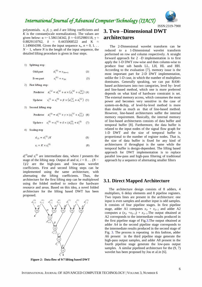
3.1. Direct Mapped Architecture
The architecture design consists of 8 adders, 4
multipliers, 6 delay elements and 8 pipeline registers.
Two inputs lines are present in the architecture: one input is even samples and another input is odd samples.
It consists of four pipeline stages. In first pipeline
stage, adder A1 computes x2i + x2i−2 and adder A2
computes a (x2i +x2i−2) + x2i−1.The output obtained at
A2 corresponds to the intermediate results produced in
the first pipeline stage of Fig.3.The output obtained at
adder A4 in the second pipeline stage corresponds to
the intermediate results produced in the second stage of
Fig. 3. The process is repeating in this fashion, adder
A6 present in the third pipeline stage generate the
high-pass output samples, and adder A8 present in the fourth pipeline stage generate the low-pass output
samples. A similar pipelined architecture for the (9, 7)
wavelet has been proposed by Jou et al.in [6].
International Journal of Advanced Computer Technology (IJACT) ISSN:2319-7900
7
A SURVEY ON VLSI ARCHITECTURES OF LIFTING-BASED 2D DISCRETE WAVELET TRANSFORM
Figure 3: Direct Mapped Architecture
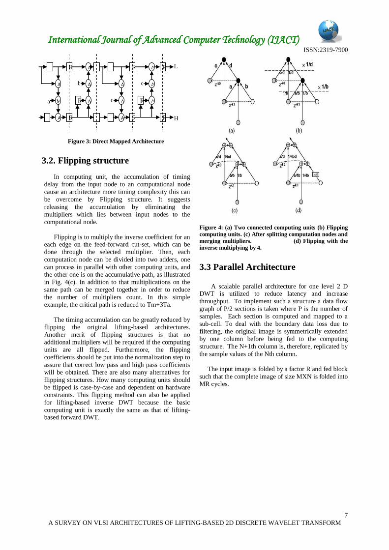
3.2. Flipping structure
In computing unit, the accumulation of timing
delay from the input node to an computational node
cause an architecture more timing complexity this can
be overcome by Flipping structure. It suggests
releasing the accumulation by eliminating the
multipliers which lies between input nodes to the
computational node.
Flipping is to multiply the inverse coefficient for an each edge on the feed-forward cut-set, which can be
done through the selected multiplier. Then, each
computation node can be divided into two adders, one
can process in parallel with other computing units, and
the other one is on the accumulative path, as illustrated
in Fig. 4(c). In addition to that multiplications on the
same path can be merged together in order to reduce
the number of multipliers count. In this simple
example, the critical path is reduced to Tm+3Ta.
The timing accumulation can be greatly reduced by flipping the original lifting-based architectures.
Another merit of flipping structures is that no
additional multipliers will be required if the computing
units are all flipped. Furthermore, the flipping
coefficients should be put into the normalization step to
assure that correct low pass and high pass coefficients
will be obtained. There are also many alternatives for
flipping structures. How many computing units should
be flipped is case-by-case and dependent on hardware
constraints. This flipping method can also be applied
for lifting-based inverse DWT because the basic
computing unit is exactly the same as that of lifting-based forward DWT.
Figure 4: (a) Two connected computing units (b) Flipping
computing units. (c) After splitting computation nodes and
merging multipliers. (d) Flipping with the
inverse multiplying by 4.
3.3 Parallel Architecture
A scalable parallel architecture for one level 2 D DWT is utilized to reduce latency and increase
throughput. To implement such a structure a data flow
graph of P/2 sections is taken where P is the number of
samples. Each section is computed and mapped to a
sub-cell. To deal with the boundary data loss due to
filtering, the original image is symmetrically extended
by one column before being fed to the computing
structure. The N+1th column is, therefore, replicated by
the sample values of the Nth column.
The input image is folded by a factor R and fed block
such that the complete image of size MXN is folded into MR cycles.
R
2
R
1
R
3
A1
R
3
D
R
1
D
R
3
R
4
D
D
R2
R
4
M
1
A2
A2
A2
A2
A2
A2
A2
A2
A2
A2
R
1 a
b
c
d
LP
HP

International Journal of Advanced Computer Technology (IJACT) ISSN:2319-7900
8
INTERNATIONAL JOURNAL OF ADVANCED COMPUTER TECHNOLOGY | VOLUME 3, NUMBER 6
Figure 5: Parallel Architecture for Multilevel lifting 2D DWT
3.4 Efficient Folded Architecture It is well known that, in the lifting scheme, the way of
processing the intermediate data determines the hardware
scale and critical path latency of the implementing
architecture. In the following, parallel and pipeline
techniques have been used to process the intermediate
data. The corresponding architecture possesses repeatable
property. Thus, it can further be improved, leading to the
EFA.
Figure 6.Efficient folded architecture
The lifting steps are fed back to pipeline registers (P1
and P2). They can be used for the second lifting step. As
a result, the first and second lifting steps are interleaved
by selecting their own coefficients. We use 4 registers
D1, D2, D3 and D4 to selecting their own coefficients.
We use 4 registers D1, D2, D3 and D4 to restore
intermediate data. In this procedure, two delay registers
D3 and D4 are needed n each lifting step for the proper
schedule. The speed of the internal processing unit is two times
that of the even (odd) input/output data.
The delay registers are represented as,
It means that the input/output data rate to the DWT
processor is one sample per clock cycle. The proposed
architecture needs only four adders and two multipliers,
which are half those of the optimized architecture.
Hardware utility obtained is 100%.
3.5. Recursive Architecture
The basic strategy of the 2-D recursive architecture is
the same as that of its 1-D counterpart: The calculations
of all DWT stages are interleaved to increase the
hardware utilization. Within each DWT stage, the processing sequence has been shown in Fig. 7. The image
is scanned into the row processor in a format, and the first
horizontal DWT is started. As a result, high- and low-
frequency DWT coefficients of odd lines are collected
International Journal of Advanced Computer Technology (IJACT) ISSN:2319-7900
9
A SURVEY ON VLSI ARCHITECTURES OF LIFTING-BASED 2D DISCRETE WAVELET TRANSFORM
and pushed into two first-in first-out (FIFO) registers or two memory banks.
Figure 7: Recursive Architecture
The separate storage of re regular data flow and
reduces the required output switch operations and it
consumes low power. The DWT coefficients of the even
lines are also rearranged into the same sequence and are
directly sent to the column processor, together with the
outputs of the FIFO. The column processor starts
calculating the vertical DWT in a zigzag format after one
row’s delay. Note that the row DWT is similar to that of
the 1-D DWT so that data path of the row processor is the
same as for the1-D RA. The column processor is implemented by replacing the delay registers and input
circuit of the 1-D RA with delay FIFOs and the circuitry,
as shown in Fig. 7. The interaction between the row and
column processor goes as follows: When the row
processor is processing the even lines (assuming that it
starts with 0th row), the high and low-frequency DWT
coefficients are shifted into their corresponding FIFOs.
When the row processor is processing the odd lines, the
low-frequency DWT coefficients of current lines and of
the previous lines stored in the FIFO s are sent to the
column processor
3.6 Two-Dimensional Dual Scan
Architecture: The vertical DWT is carried out only after the
horizontal DWT is finished. The delay between the row
and column computations limits the processing speed.
The 2 –D DSA shortens the delay by adopting a new scan
sequence. In applications that can read two pixels per
clock cycle from data buffer, the scan sequence of the 2-D
DSA, which is shown in figure 8, can be used
The row processor scans along two consecutive rows
simultaneously, whereas the column processor also
horizontally scans in the row DWT coefficients. In this
way, the column processor can start its computation as soon as the first pair of row DWT coefficients is ready.
With this improvement, the row and column processors
compute the same stage DWT within a few clock cycles of
each other. The registers are used to separately hold the
even and odd pixels of each row and to interleave the input
pairs of each two consecutive rows. The row processor of
the 2-D DSA is identical to the direct implementation of
the 1-D DWT. The column processor is obtained by
replacing the 1-pixel delay units in the row processor with
1-row delay units. The low-frequency output switch of the
column processor directs the LL sub band of each stage
DWT to the memory bank.
The LL sub image stored in the memory will be
returned to the DSA input for further decomposition after
the current DWT stage is finished. The comparisons of
the processing time and memory size are shown in Table
1, respectively. The timing for the RA is based on one
input pixel per clock cycle, whereas the others are based
on two input pixels per cycle.
Figure 8: Two dimensional DSA
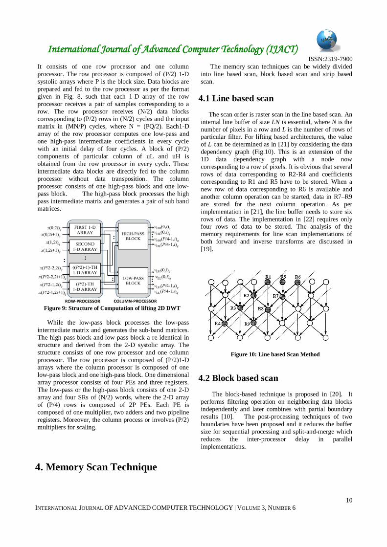
3.7 Systolic Array The structure of the area efficient lifting based architecture of DWT in 2 dimensions is shown in Fig. 9.
International Journal of Advanced Computer Technology (IJACT) ISSN:2319-7900
10
INTERNATIONAL JOURNAL OF ADVANCED COMPUTER TECHNOLOGY | VOLUME 3, NUMBER 6
It consists of one row processor and one column
processor. The row processor is composed of (P/2) 1-D
systolic arrays where P is the block size. Data blocks are
prepared and fed to the row processor as per the format
given in Fig. 8, such that each 1-D array of the row
processor receives a pair of samples corresponding to a
row. The row processor receives (N/2) data blocks corresponding to (P/2) rows in (N/2) cycles and the input
matrix in (MN/P) cycles, where N = (PQ/2). Each1-D
array of the row processor computes one low-pass and
one high-pass intermediate coefficients in every cycle
with an initial delay of four cycles. A block of (P/2)
components of particular column of uL and uH is
obtained from the row processor in every cycle. These
intermediate data blocks are directly fed to the column
processor without data transposition. The column
processor consists of one high-pass block and one low-
pass block. The high-pass block processes the high
pass intermediate matrix and generates a pair of sub band matrices.
Figure 9: Structure of Computation of lifting 2D DWT
While the low-pass block processes the low-pass
intermediate matrix and generates the sub-band matrices.
The high-pass block and low-pass block a re-identical in
structure and derived from the 2-D systolic array. The
structure consists of one row processor and one column
processor. The row processor is composed of (P/2)1-D arrays where the column processor is composed of one
low-pass block and one high-pass block. One dimensional
array processor consists of four PEs and three registers.
The low-pass or the high-pass block consists of one 2-D
array and four SRs of (N/2) words, where the 2-D array
of (P/4) rows is composed of 2P PEs. Each PE is
composed of one multiplier, two adders and two pipeline
registers. Moreover, the column process or involves (P/2)
multipliers for scaling.
4. Memory Scan Technique
The memory scan techniques can be widely divided
into line based scan, block based scan and strip based
scan.
4.1 Line based scan
The scan order is raster scan in the line based scan. An
internal line buffer of size LN is essential, where N is the
number of pixels in a row and L is the number of rows of particular filter. For lifting based architectures, the value
of L can be determined as in [21] by considering the data
dependency graph (Fig.10). This is an extension of the
1D data dependency graph with a node now
corresponding to a row of pixels. It is obvious that several
rows of data corresponding to R2-R4 and coefficients
corresponding to R1 and R5 have to be stored. When a
new row of data corresponding to R6 is available and
another column operation can be started, data in R7–R9
are stored for the next column operation. As per
implementation in [21], the line buffer needs to store six
rows of data. The implementation in [22] requires only four rows of data to be stored. The analysis of the
memory requirements for line scan implementations of
both forward and inverse transforms are discussed in
[19].
Figure 10: Line based Scan Method
4.2 Block based scan
The block-based technique is proposed in [20]. It
performs filtering operation on neighboring data blocks
independently and later combines with partial boundary
results [10]. The post-processing techniques of two
boundaries have been proposed and it reduces the buffer
size for sequential processing and split-and-merge which
reduces the inter-processor delay in parallel
implementations.
International Journal of Advanced Computer Technology (IJACT) ISSN:2319-7900
11
A SURVEY ON VLSI ARCHITECTURES OF LIFTING-BASED 2D DISCRETE WAVELET TRANSFORM
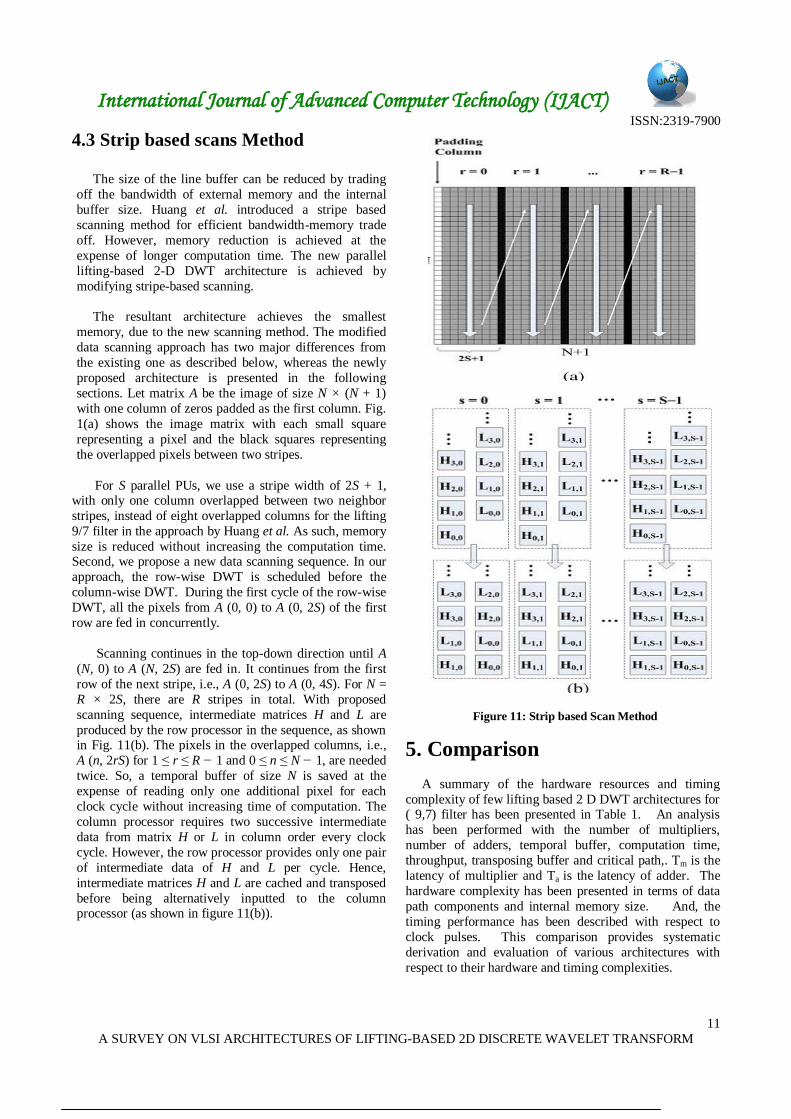
4.3 Strip based scans Method
The size of the line buffer can be reduced by trading
off the bandwidth of external memory and the internal
buffer size. Huang et al. introduced a stripe based
scanning method for efficient bandwidth-memory trade
off. However, memory reduction is achieved at the
expense of longer computation time. The new parallel
lifting-based 2-D DWT architecture is achieved by
modifying stripe-based scanning.
The resultant architecture achieves the smallest
memory, due to the new scanning method. The modified
data scanning approach has two major differences from
the existing one as described below, whereas the newly
proposed architecture is presented in the following
sections. Let matrix A be the image of size N × (N + 1)
with one column of zeros padded as the first column. Fig.
1(a) shows the image matrix with each small square
representing a pixel and the black squares representing
the overlapped pixels between two stripes.
For S parallel PUs, we use a stripe width of 2S + 1, with only one column overlapped between two neighbor
stripes, instead of eight overlapped columns for the lifting
9/7 filter in the approach by Huang et al. As such, memory
size is reduced without increasing the computation time. Second, we propose a new data scanning sequence. In our
approach, the row-wise DWT is scheduled before the
column-wise DWT. During the first cycle of the row-wise
DWT, all the pixels from A (0, 0) to A (0, 2S) of the first
row are fed in concurrently.
Scanning continues in the top-down direction until A
(N, 0) to A (N, 2S) are fed in. It continues from the first
row of the next stripe, i.e., A (0, 2S) to A (0, 4S). For N =
R × 2S, there are R stripes in total. With proposed
scanning sequence, intermediate matrices H and L are
produced by the row processor in the sequence, as shown in Fig. 11(b). The pixels in the overlapped columns, i.e.,
A (n, 2rS) for 1 ≤ r ≤ R − 1 and 0 ≤ n ≤ N − 1, are needed
twice. So, a temporal buffer of size N is saved at the
expense of reading only one additional pixel for each
clock cycle without increasing time of computation. The
column processor requires two successive intermediate
data from matrix H or L in column order every clock
cycle. However, the row processor provides only one pair
of intermediate data of H and L per cycle. Hence,
intermediate matrices H and L are cached and transposed
before being alternatively inputted to the column processor (as shown in figure 11(b)).
Figure 11: Strip based Scan Method
5. Comparison
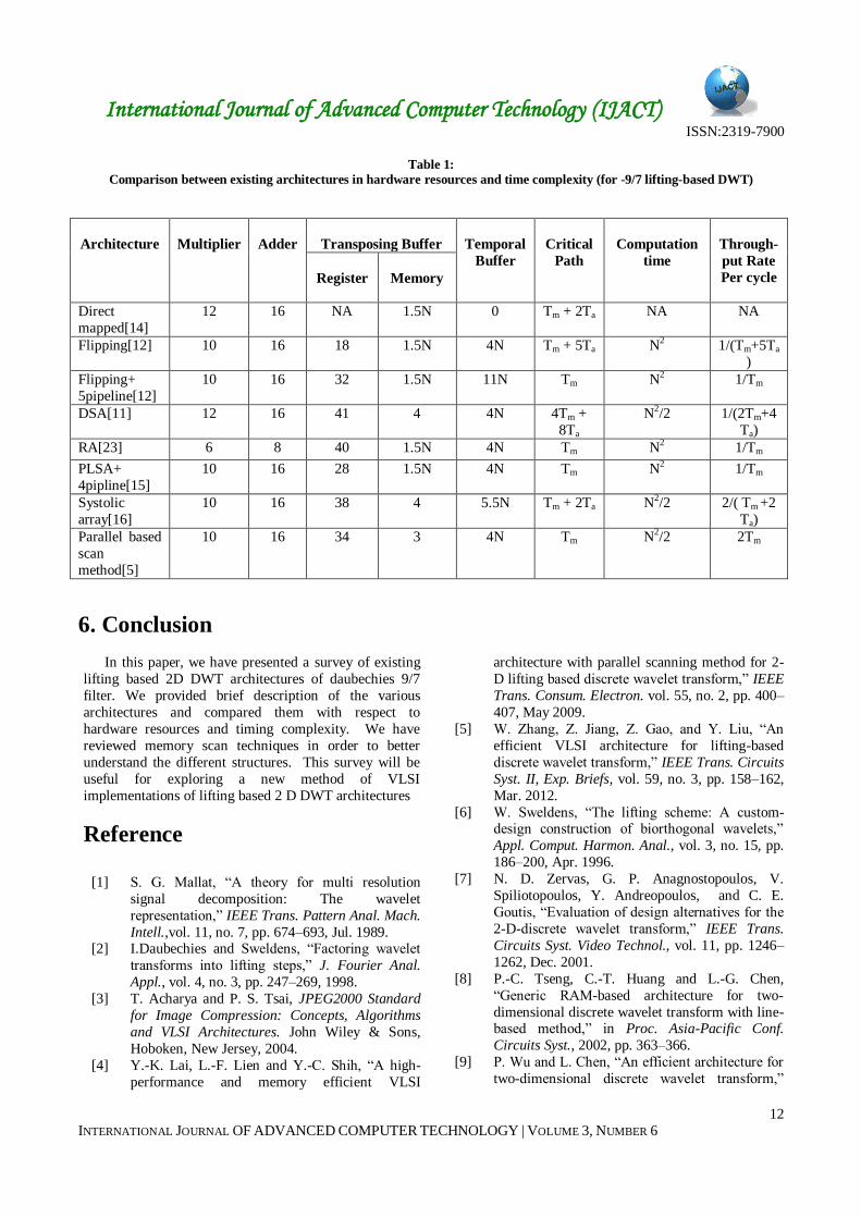
A summary of the hardware resources and timing
complexity of few lifting based 2 D DWT architectures for ( 9,7) filter has been presented in Table 1. An analysis
has been performed with the number of multipliers,
number of adders, temporal buffer, computation time,
throughput, transposing buffer and critical path,. Tm is the
latency of multiplier and Ta is the latency of adder. The
hardware complexity has been presented in terms of data
path components and internal memory size. And, the
timing performance has been described with respect to
clock pulses. This comparison provides systematic
derivation and evaluation of various architectures with
respect to their hardware and timing complexities.
International Journal of Advanced Computer Technology (IJACT) ISSN:2319-7900
12
INTERNATIONAL JOURNAL OF ADVANCED COMPUTER TECHNOLOGY | VOLUME 3, NUMBER 6
Table 1:
Comparison between existing architectures in hardware resources and time complexity (for -9/7 lifting-based DWT)
Architecture
Multiplier
Adder
Transposing Buffer
Temporal
Buffer
Critical
Path
Computation
time
Through-
put Rate
Per cycle
Register
Memory
Direct
mapped[14]
12 16 NA 1.5N 0 Tm + 2Ta NA NA
Flipping[12] 10 16 18 1.5N 4N Tm + 5Ta N2 1/(Tm+5Ta
)
Flipping+
5pipeline[12]
10 16 32 1.5N 11N Tm N2 1/Tm
DSA[11] 12 16 41 4 4N 4Tm +
8Ta
N2/2 1/(2Tm+4
Ta)
RA[23] 6 8 40 1.5N 4N Tm N2 1/Tm
PLSA+
4pipline[15]
10 16 28 1.5N 4N Tm N2 1/Tm
Systolic
array[16]
10 16 38 4 5.5N Tm + 2Ta N2/2 2/( Tm +2
Ta)
Parallel based
scan
method[5]
10 16 34 3 4N Tm N2/2 2Tm
6. Conclusion
In this paper, we have presented a survey of existing
lifting based 2D DWT architectures of daubechies 9/7
filter. We provided brief description of the various
architectures and compared them with respect to
hardware resources and timing complexity. We have
reviewed memory scan techniques in order to better
understand the different structures. This survey will be
useful for exploring a new method of VLSI
implementations of lifting based 2 D DWT architectures
Reference
[1] S. G. Mallat, “A theory for multi resolution
signal decomposition: The wavelet
representation,” IEEE Trans. Pattern Anal. Mach.
Intell.,vol. 11, no. 7, pp. 674–693, Jul. 1989. [2] I.Daubechies and Sweldens, “Factoring wavelet
transforms into lifting steps,” J. Fourier Anal.
Appl., vol. 4, no. 3, pp. 247–269, 1998.
[3] T. Acharya and P. S. Tsai, JPEG2000 Standard
for Image Compression: Concepts, Algorithms
and VLSI Architectures. John Wiley & Sons,
Hoboken, New Jersey, 2004.
[4] Y.-K. Lai, L.-F. Lien and Y.-C. Shih, “A high-
performance and memory efficient VLSI
architecture with parallel scanning method for 2-
D lifting based discrete wavelet transform,” IEEE
Trans. Consum. Electron. vol. 55, no. 2, pp. 400–
407, May 2009.
[5] W. Zhang, Z. Jiang, Z. Gao, and Y. Liu, “An
efficient VLSI architecture for lifting-based
discrete wavelet transform,” IEEE Trans. Circuits
Syst. II, Exp. Briefs, vol. 59, no. 3, pp. 158–162,
Mar. 2012.
[6] W. Sweldens, “The lifting scheme: A custom-design construction of biorthogonal wavelets,”
Appl. Comput. Harmon. Anal., vol. 3, no. 15, pp.
186–200, Apr. 1996.
[7] N. D. Zervas, G. P. Anagnostopoulos, V.
Spiliotopoulos, Y. Andreopoulos, and C. E.
Goutis, “Evaluation of design alternatives for the
2-D-discrete wavelet transform,” IEEE Trans.
Circuits Syst. Video Technol., vol. 11, pp. 1246–
1262, Dec. 2001.
[8] P.-C. Tseng, C.-T. Huang and L.-G. Chen,
“Generic RAM-based architecture for two-
dimensional discrete wavelet transform with line-based method,” in Proc. Asia-Pacific Conf.
Circuits Syst., 2002, pp. 363–366.
[9] P. Wu and L. Chen, “An efficient architecture for
two-dimensional discrete wavelet transform,”
International Journal of Advanced Computer Technology (IJACT) ISSN:2319-7900
13
A SURVEY ON VLSI ARCHITECTURES OF LIFTING-BASED 2D DISCRETE WAVELET TRANSFORM
IEEE Trans. Circuits Syst. Video Technol., vol.
11, pp. 536–544, Apr. 2001.
[10] N.Usha bhanu, A.Chilambuchelvan, “High speed
VLSI architecture for non separable block based
lifting wavelet transform”, Journal of Theoretical
and Applied Information Technology , vol. 63,
no. 3, pp.626-635, May 2014. [11] H. Liao, M. K. Mandal, and B. F. Cockburn,
“Efficient architectures for 1-D and 2-D lifting-
based wavelet transforms,” IEEE Trans. Signal
Process., vol.52, no.5,pp. 1315-1326, May 2004.
[12] C.-T. Huang, P.-C. Tseng and L.-G. Chen,
“Flipping structure: An efficient VLSI
architecture for lifting-based discrete wavelet
transform.” IEEE Trans. Signal Process. vol. 52.
No. 4, pp. 1080-1089, April 2004.
[13] G.-M. Shi,W.-F. Liu, L. Zhang, and F. Li, “An
efficient folded architecture for lifting-based
discrete wavelet transform,” IEEE Trans. Circuits
Syst. II, Exp. Briefs, vol. 56, no. 4, pp. 290–294,
Apr. 2009.
[14] J. M. Jou, Y. H. Shiau, and C. C. Liu,
“Efficient VLSI architectures for the bio
orthogonal wavelet transform by filter bank and
lifting scheme,” in Proc. IEEE Int. Symp. Circuits
Syst., 2001, pp. 529–532. [15] C.-Y. Xiong, J.-W. Tian, and J. Liu, “A note on
‘flipping structure: An efficient VLSI architecture
for lifting-based discrete wavelet transform’,”
IEEE Trans. Signal Process., vol. 54, no. 5, pp.
1910–1916, May 2006
[16] B. K. Mohanty, A. Mahajan, and P. K. Meher,
“Area- and power-efficient architecture for high-
throughput implementation of lifting 2-D DWT,”
IEEE Trans. Circuits Syst. II, Exp. Briefs, vol. 59,
no. 7, pp. 434–438,Jul. 2012.
[17] yusong Hu and Ching Chuen Jong “A Memory-Efficient scalable Architecture for Lifting-Based
Discrete Wavelet Transform” IEEE Trans.
Circuits Sys. II, Exp. Briefs, vol. 60, no. 8, pp.
502-506, Aug. 2012.
[18] C. Chrysafis and A. Ortega, “Line-Based,
Reduced Memory, Wavelet Image Compression,”
IEEE Trans. on Image Processing, vol. 9, no. 3,
2000, pp. 378–389.
[19] J. Reichel, M. Nadenau, and M. Kunt, “Row-
Based Wavelet Decomposition Using the Lifting
Scheme,” Procee dings of the Workshop on
Wavelet Transforms and Filter Banks, Brandenburgan der Havel, Germany, March 5–7,
1999.
[20] W. Jiang and A. Ortega, “Lifting Factorization-
Based Discrete Wavelet Transform Architecture
Design,” IEEE Trans, on Circuits and Systems
for Video Technology, vol. 11, pp. 651–657,
2001.
[21] M.Y. Chiu, K.-B. Lee and C.-W. Jen, “Optimal
Data Transfer and Buffering Schemes for JPEG
20000 Encoder,” in Proceedings of the IEEE
Workshop on Design and Implementation of Signal Processing Systems, pp. 177–182, 2003.
[22] C.-T. Huang, P.-C. Tseng and L.-G. Chen,
“Memory Analysis and Architecture Wavelet
Transform,” in Proceedings of IEEE Int. Conf. on
Acoustics, Speech and Signal Processing, pp. V13-V16, 2004.
[23] B. F. Wu and C. F. Lin, “A high-performance
and memory-efficient pipeline architecture for the
5/3 and 9/7 discrete wavelet transform of
JPEG2000 codec,” IEEE Trans. Circuits Syst.
Video Technol., vol. 15, no. 12, pp. 1615–1628,
Dec. 2005
Biographies
S.SENTHILKUMAR received the B.E degree in
Electronics and Communication Engineering from
Bharathiar University, coimbatore and M.E. Degree in
Applied Electronics from Anna University, Chennai, in
1998 and 2004, respectively. He is currently pursuing his
part time Ph.D. degree in the field of VLSI design of image processing architecture in Anna University,
chennai. Presently, he is working as an Associate
Professor in SVS college of Engineering, Coimbatore,
Tamilnadu, India.
Dr.R.RADHAKRISHNAN is currently Principal, Vidya
Mandhir Institute of Technology, Erode, Tamil Nadu,
India. He received his Master Degree from P.S.G. College
of Technology, Coimbatore, in the year 1997 and the PhD
from Anna University, Chennai in the year 2008.
M.GOKULAKRISHNAN, Department of Electronics
and Communication Engineering, is doing M.E (VLSI
Design), SVS College of Engineering, Coimbatore,
Tamilnadu, India.
Recommended