
ELE3230 - Chapter 12 2
Introduction to Input-Output
CPU
Memoryinterface
I/O interface
MEMORY
Outside worldeg. keyboardprinterCRT displaymass storage
addressaddress &control
data bus
I/O address& control
ELE3230 - Chapter 12 3
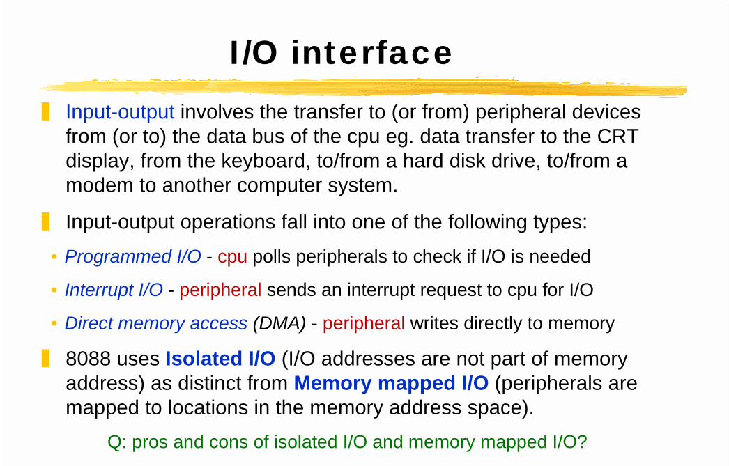
I/O interface Input-output involves the transfer to (or from) peripheral devices
from (or to) the data bus of the cpu eg. data transfer to the CRTdisplay, from the keyboard, to/from a hard disk drive, to/from amodem to another computer system.
Input-output operations fall into one of the following types: • Programmed I/O - cpu polls peripherals to check if I/O is needed
• Interrupt I/O - peripheral sends an interrupt request to cpu for I/O
• Direct memory access (DMA) - peripheral writes directly to memory
8088 uses Isolated I/O (I/O addresses are not part of memoryaddress) as distinct from Memory mapped I/O (peripherals aremapped to locations in the memory address space).
Q: pros and cons of isolated I/O and memory mapped I/O?
ELE3230 - Chapter 12 4
1M × 8
MemoryFFFFF
00000
FFFF
64K × 8
I/O
0000(a)
Memory + I/O
I/O
FFFFF
00000(b)
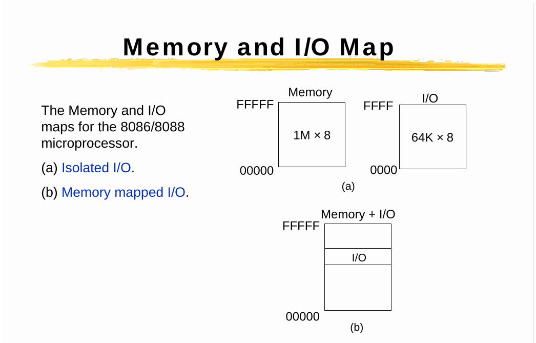
The Memory and I/Omaps for the 8086/8088microprocessor.
(a) Isolated I/O.
(b) Memory mapped I/O.
Memory and I/O Map
ELE3230 - Chapter 12 5
I/O interface
data buffer registers
status register
I/O protocol unit
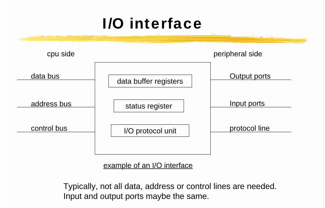
cpu side peripheral side
data bus
address bus
control bus
Output ports
Input ports
protocol line
example of an I/O interface
Typically, not all data, address or control lines are needed. Input and output ports maybe the same.
ELE3230 - Chapter 12 6
I/O interface I/O interface functions can include • data storage buffer for sending and receiving data • low-level communications protocol (handshaking) • data format conversion (eg. parallel/serial) • error detection • addressing of different peripherals
I/O interface are typically implemented by LSI (large scaleintegration) - many different types are available from differentmanufacturers.
Data can be transferred through I/O interface by eitherprogrammed I/O or interrupt I/O. DMA typically needs a separatecontroller.
ELE3230 - Chapter 12 7
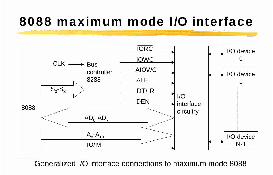
8088 maximum mode I/O interface
AIOWC
8088
Buscontroller8288
I/Ointerfacecircuitry
I/O device1
I/O deviceN-1
I/O device0
A8-A19
AD0-AD7
S0-S3
CLK
DEN
ALE
Generalized I/O interface connections to maximum mode 8088
IORCIOWC
RDT/
MIO/
ELE3230 - Chapter 12 9
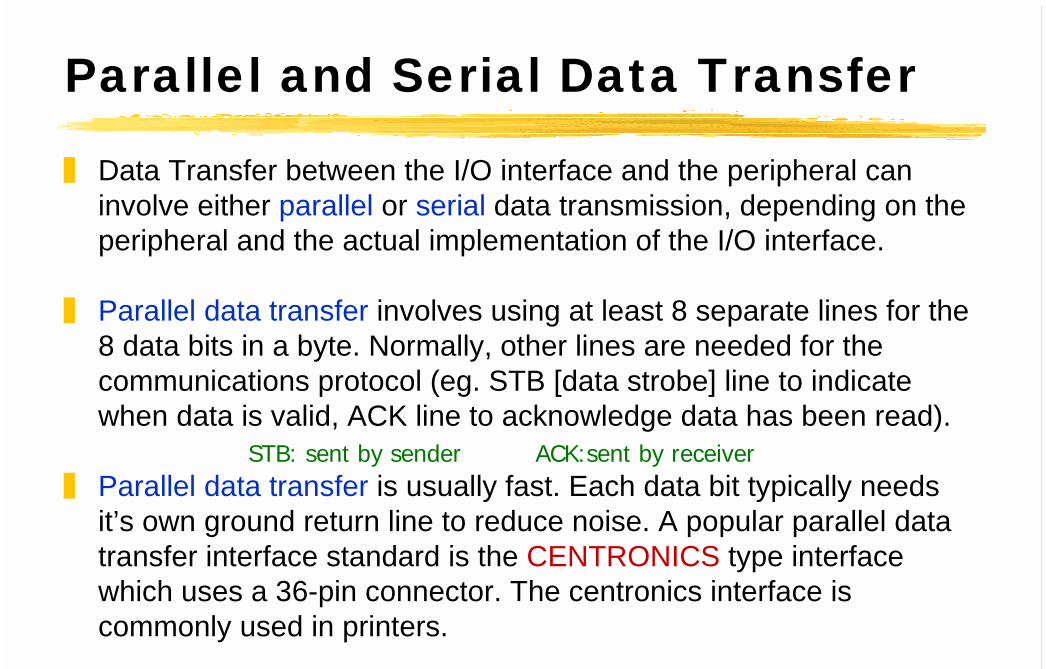
Parallel and Serial Data Transfer
Data Transfer between the I/O interface and the peripheral caninvolve either parallel or serial data transmission, depending on theperipheral and the actual implementation of the I/O interface.
Parallel data transfer involves using at least 8 separate lines for the8 data bits in a byte. Normally, other lines are needed for thecommunications protocol (eg. STB [data strobe] line to indicatewhen data is valid, ACK line to acknowledge data has been read).
Parallel data transfer is usually fast. Each data bit typically needsit’s own ground return line to reduce noise. A popular parallel datatransfer interface standard is the CENTRONICS type interfacewhich uses a 36-pin connector. The centronics interface iscommonly used in printers.
STB: sent by sender ACK:sent by receiver
ELE3230 - Chapter 12 10
Parallel and Serial Data Transfer(cont.)
Serial data transfer involves sending the data on a single line, bitby bit. The I/O interface converts the data from parallel to serial orvice-versa using shift registers.
Serial connections are commonly used for data transfer overlonger distances (eg over telephone line). A popular standard forserial data transmission is the RS232C standard.
ELE3230 - Chapter 12 11
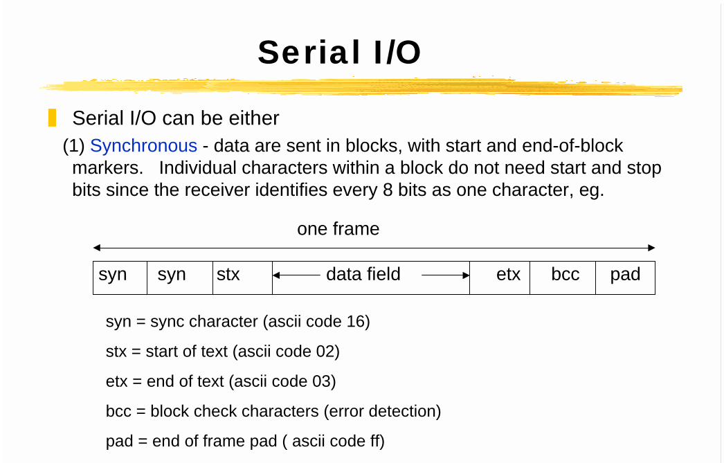
Serial I/O
Serial I/O can be either (1) Synchronous - data are sent in blocks, with start and end-of-block
markers. Individual characters within a block do not need start and stopbits since the receiver identifies every 8 bits as one character, eg.
syn syn stx data field etx bcc pad
one frame
syn = sync character (ascii code 16)
stx = start of text (ascii code 02)
etx = end of text (ascii code 03)
bcc = block check characters (error detection)
pad = end of frame pad ( ascii code ff)
ELE3230 - Chapter 12 12
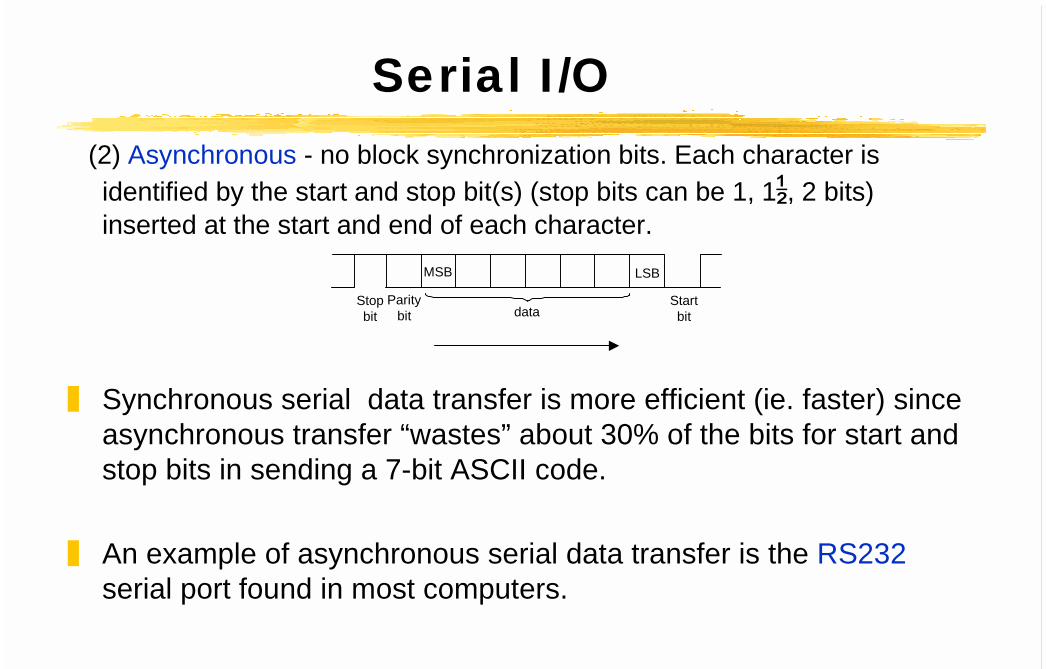
Serial I/O (2) Asynchronous - no block synchronization bits. Each character is
identified by the start and stop bit(s) (stop bits can be 1, 1!, 2 bits)inserted at the start and end of each character.
Synchronous serial data transfer is more efficient (ie. faster) sinceasynchronous transfer “wastes” about 30% of the bits for start andstop bits in sending a 7-bit ASCII code.
An example of asynchronous serial data transfer is the RS232serial port found in most computers.
LSBMSB
Startbit
Stopbit
Paritybit data
ELE3230 - Chapter 12 13
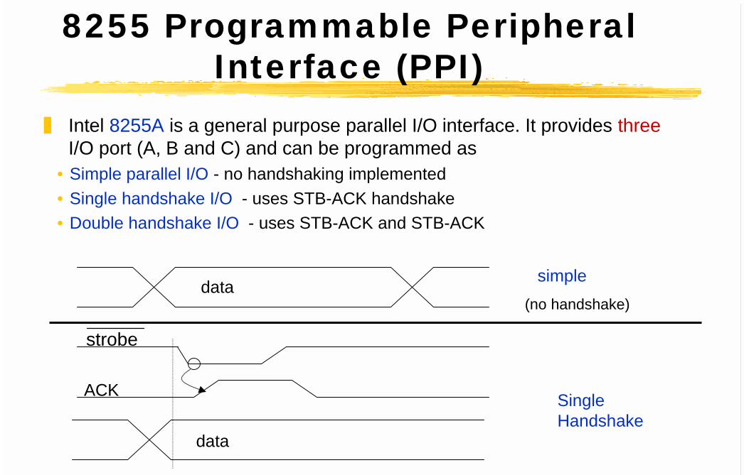
8255 Programmable PeripheralInterface (PPI)
Intel 8255A is a general purpose parallel I/O interface. It provides threeI/O port (A, B and C) and can be programmed as
• Simple parallel I/O - no handshaking implemented • Single handshake I/O - uses STB-ACK handshake • Double handshake I/O - uses STB-ACK and STB-ACK
data
SingleHandshake
data simple (no handshake)
ACK
strobe
ELE3230 - Chapter 12 14
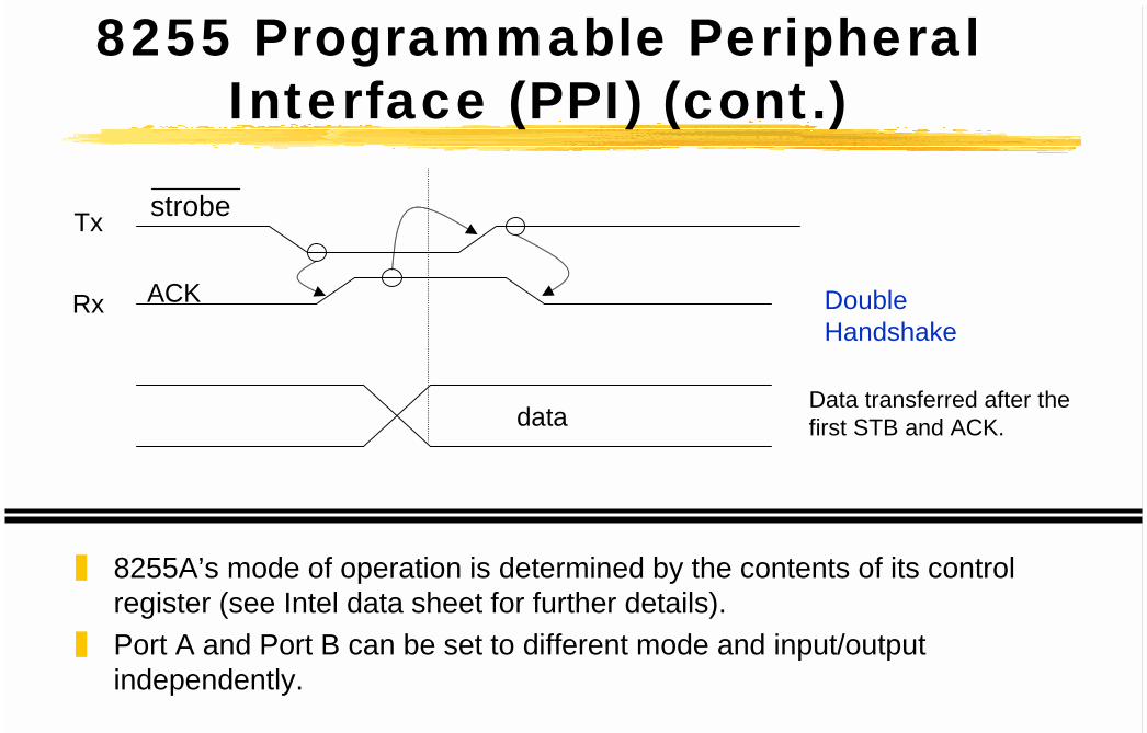
8255 Programmable PeripheralInterface (PPI) (cont.)
8255A’s mode of operation is determined by the contents of its controlregister (see Intel data sheet for further details).
Port A and Port B can be set to different mode and input/outputindependently.
data
DoubleHandshake
ACK
strobe
Data transferred after thefirst STB and ACK.
Tx
Rx
ELE3230 - Chapter 12 15
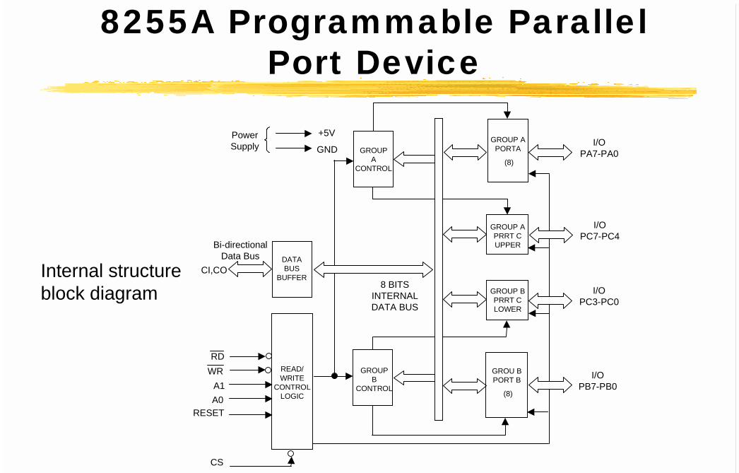
8255A Programmable ParallelPort Device
Internal structureblock diagram GROUP B
PRRT CLOWER
GROUP APRRT CUPPER
GROU BPORT B
(8)
8 BITSINTERNALDATA BUS
Bi-directionalData Bus
CI,CODATABUS
BUFFER
RDWR
A1A0
RESET
CS
READ/WRITE
CONTROLLOGIC
PowerSupply
+5V
GND GROUPA
CONTROL
GROUPB
CONTROL
GROUP APORTA
(8)
I/OPA7-PA0
I/OPC7-PC4
I/OPC3-PC0
I/OPB7-PB0
ELE3230 - Chapter 12 16
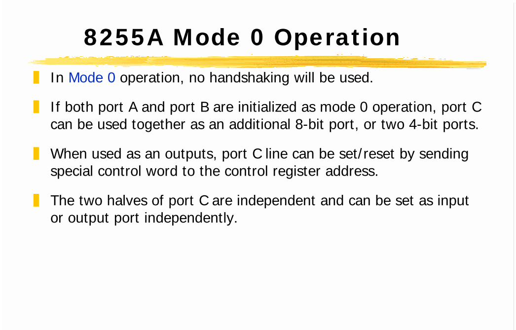
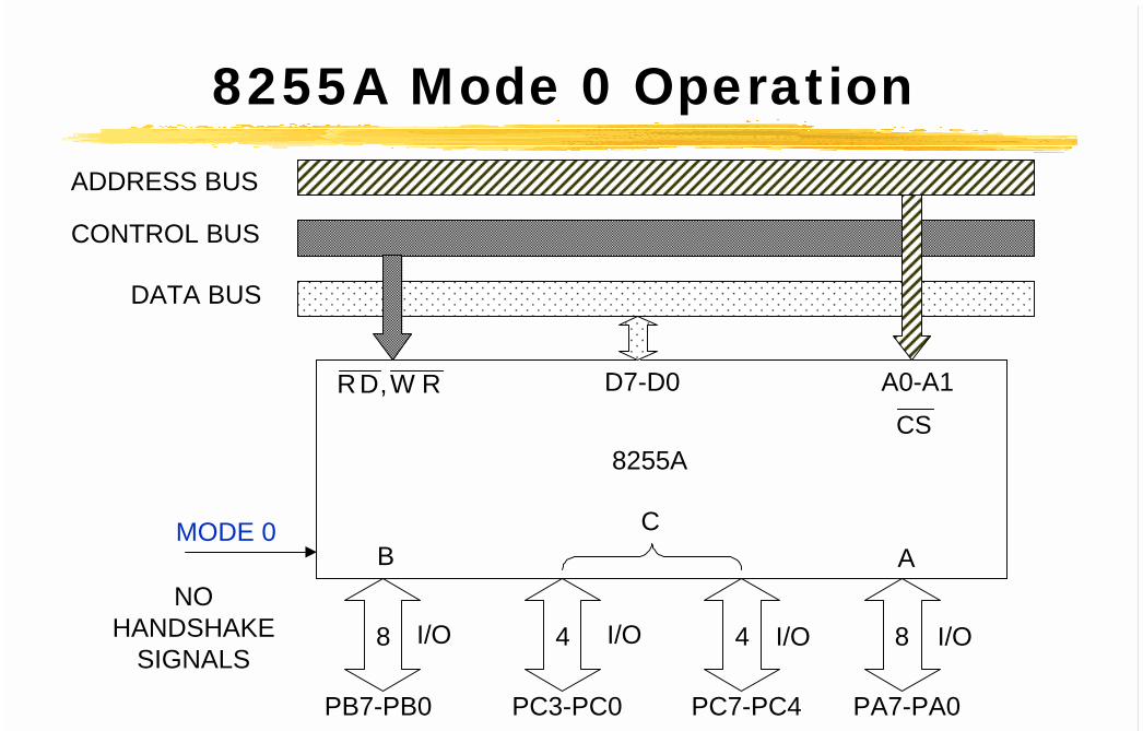
8255A Mode 0 Operation In Mode 0 operation, no handshaking will be used.
If both port A and port B are initialized as mode 0 operation, port Ccan be used together as an additional 8-bit port, or two 4-bit ports.
When used as an outputs, port C line can be set/reset by sendingspecial control word to the control register address.
The two halves of port C are independent and can be set as inputor output port independently.
ELE3230 - Chapter 12 17
8255A Mode 0 Operation
8255A
PB7-PB0 PC3-PC0 PC7-PC4 PA7-PA0
I/O I/O I/OI/O 848 4
MODE 0
NOHANDSHAKE
SIGNALS
B AC
RD,W RCS
D7-D0 A0-A1
ADDRESS BUS
CONTROL BUS
DATA BUS
ELE3230 - Chapter 12 18
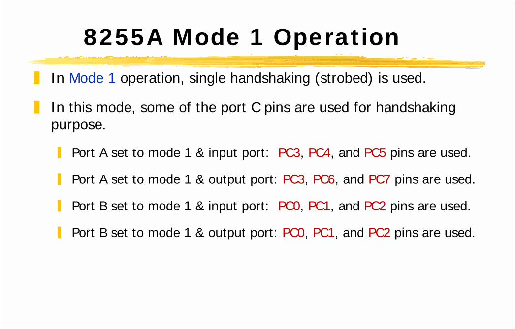
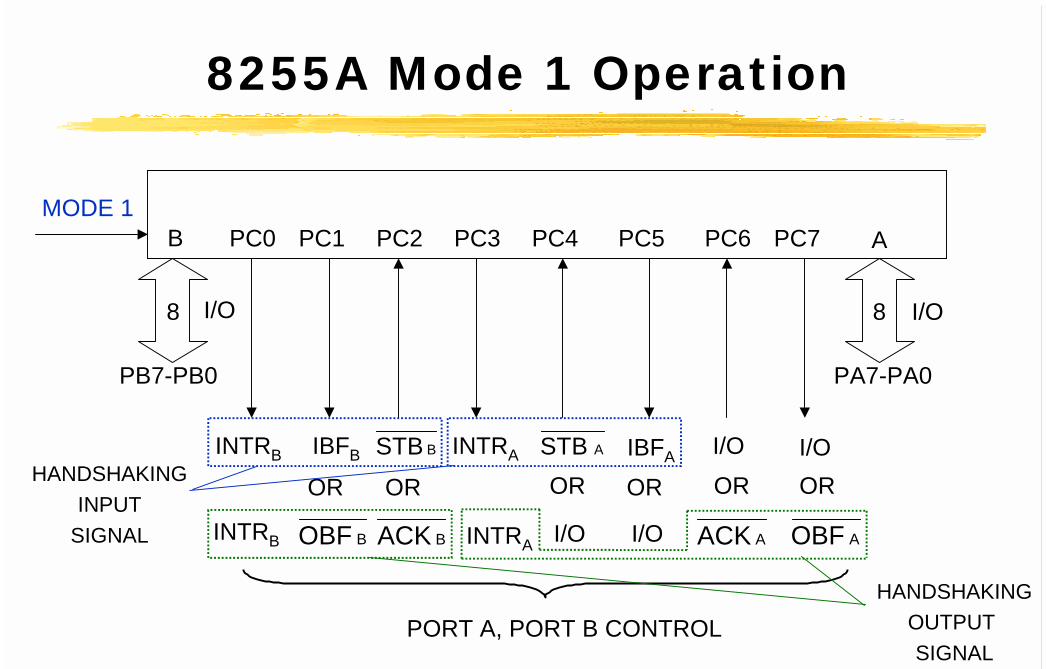
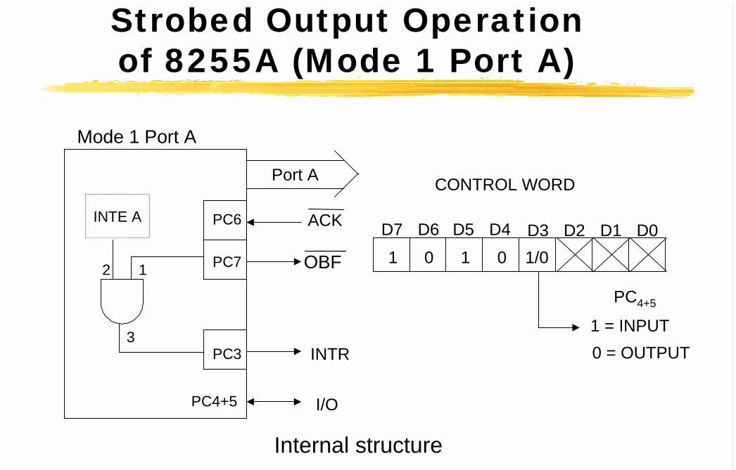
8255A Mode 1 Operation In Mode 1 operation, single handshaking (strobed) is used.
In this mode, some of the port C pins are used for handshakingpurpose.
Port A set to mode 1 & input port: PC3, PC4, and PC5 pins are used.
Port A set to mode 1 & output port: PC3, PC6, and PC7 pins are used.
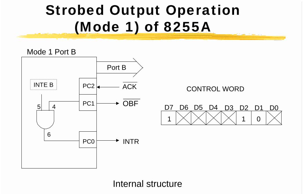
Port B set to mode 1 & input port: PC0, PC1, and PC2 pins are used.
Port B set to mode 1 & output port: PC0, PC1, and PC2 pins are used.
ELE3230 - Chapter 12 19
8255A Mode 1 Operation
MODE 1
PB7-PB0 PA7-PA0
I/O I/O88
B APC4PC3 PC5PC1 PC2 PC6 PC7PC0
I/O
I/O AACK
OR ORI/O
I/O
OROROR ORINTRB INTRA
BOBF AOBFBACK
IBFB IBFABSTB ASTB
PORT A, PORT B CONTROL
HANDSHAKINGINPUT
SIGNAL
HANDSHAKINGOUTPUT SIGNAL
INTRB INTRA
ELE3230 - Chapter 12 20
8255A Mode 2 Operation
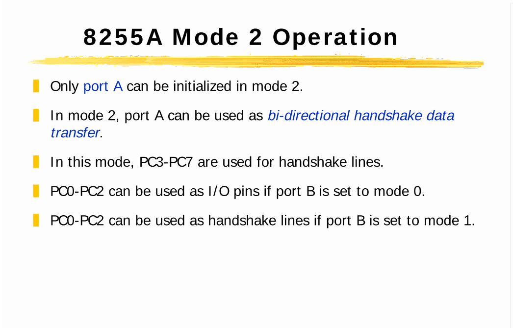
Only port A can be initialized in mode 2.
In mode 2, port A can be used as bi-directional handshake datatransfer.
In this mode, PC3-PC7 are used for handshake lines.
PC0-PC2 can be used as I/O pins if port B is set to mode 0.
PC0-PC2 can be used as handshake lines if port B is set to mode 1.

ELE3230 - Chapter 12 21
Summary of Port C Usage
MODE 2for port A
PB7-PB0 PA7-PA0
I/O I/O88
B APC4PC3 PC5PC1 PC2 PC6 PC7PC0
AACKINTRA AOBFIBFAASTB
I/O OR CONTROL
PORT B MAY BE MODE 0OR MODE 1
PORT A CONTROL
BI-DIRECTIONAL
BUS
ELE3230 - Chapter 12 22
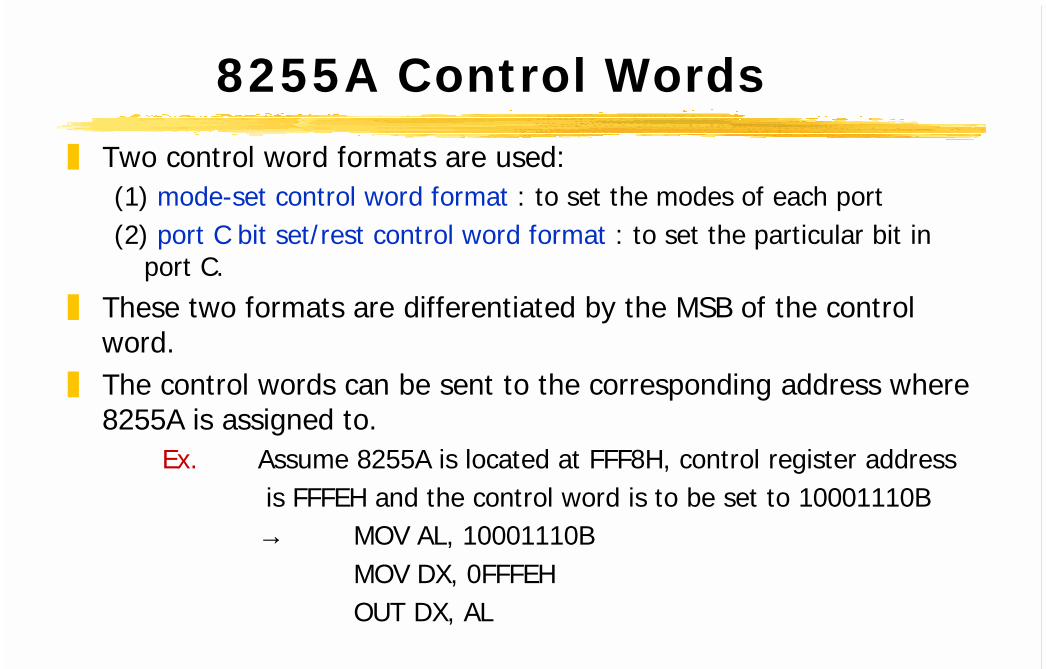
8255A Control Words Two control word formats are used:
(1) mode-set control word format : to set the modes of each port(2) port C bit set/rest control word format : to set the particular bit in
port C.
These two formats are differentiated by the MSB of the controlword.
The control words can be sent to the corresponding address where8255A is assigned to.
Ex. Assume 8255A is located at FFF8H, control register address is FFFEH and the control word is to be set to 10001110B→ MOV AL, 10001110B
MOV DX, 0FFFEHOUT DX, AL
ELE3230 - Chapter 12 23
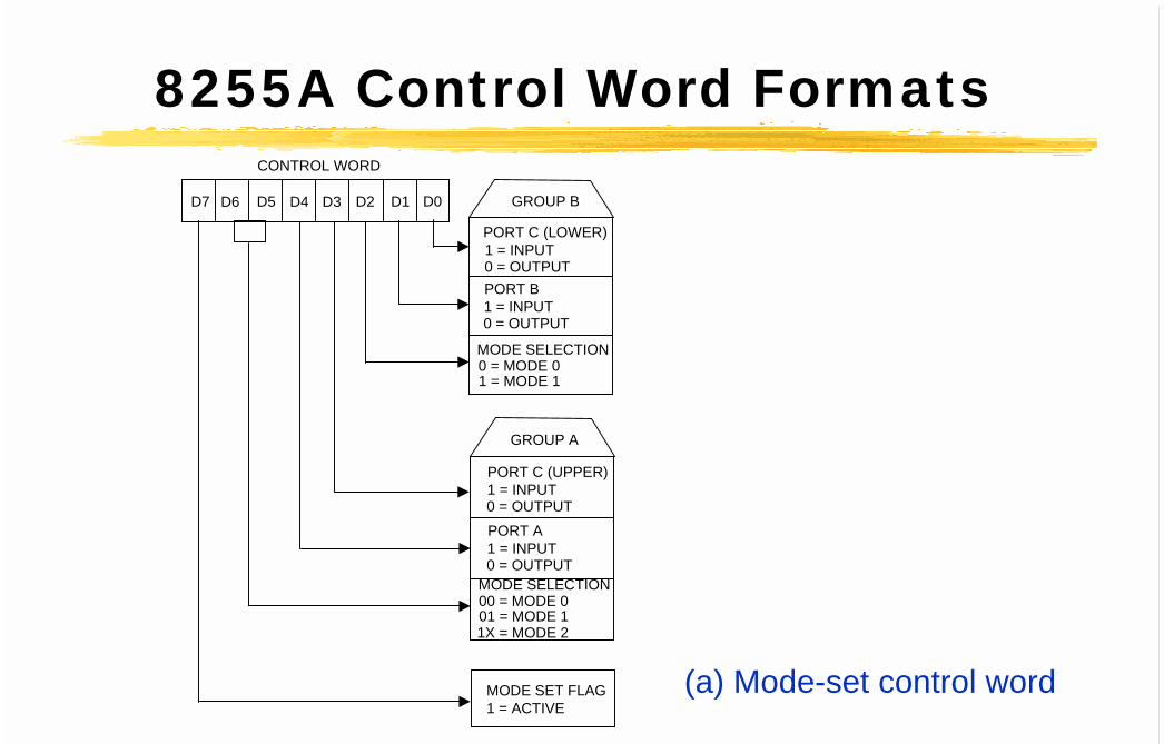
8255A Control Word Formats
(a) Mode-set control word
GROUP B
PORT C (LOWER)1 = INPUT0 = OUTPUTPORT B1 = INPUT0 = OUTPUT
MODE SELECTION0 = MODE 01 = MODE 1
GROUP A
PORT C (UPPER)1 = INPUT0 = OUTPUTPORT A1 = INPUT0 = OUTPUT
MODE SELECTION00 = MODE 001 = MODE 11X = MODE 2
MODE SET FLAG1 = ACTIVE
D7 D6 D5 D4 D3 D2 D1 D0
CONTROL WORD
ELE3230 - Chapter 12 24
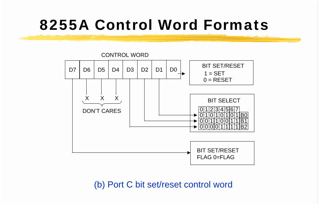
8255A Control Word Formats
(b) Port C bit set/reset control word
D7 D6 D5 D4 D3 D2 D1 D0
CONTROL WORD
X X X
DON’T CARES
BIT SET/RESET1 = SET0 = RESET
10 2 3 4 5 6 710 0 1 0 1 0 100 1 1 0 0 1 100 0 0 1 1 1 1
B0B1B2
BIT SELECT
BIT SET/RESETFLAG 0=FLAG
ELE3230 - Chapter 12 25
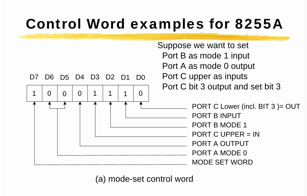
Control Word examples for 8255A
PORT C Lower (incl. BIT 3 )= OUTPORT B INPUTPORT B MODE 1PORT C UPPER = INPORT A OUTPUTPORT A MODE 0MODE SET WORD
Suppose we want to set Port B as mode 1 input Port A as mode 0 output Port C upper as inputs Port C bit 3 output and set bit 3
1
D7
0
D6
0
D5
0
D4
1
D3
1
D2
1
D1
0
D0
(a) mode-set control word
ELE3230 - Chapter 12 26
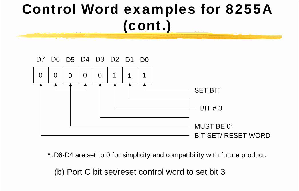
Control Word examples for 8255A(cont.)
0
D7
0
D6
0
D5
0
D4
0
D3
1
D2
1
D1
1
D0
(b) Port C bit set/reset control word to set bit 3
SET BIT
BIT # 3
MUST BE 0*BIT SET/ RESET WORD
*:D6-D4 are set to 0 for simplicity and compatibility with future product.
ELE3230 - Chapter 12 27
Strobed Output Operationof 8255A (Mode 1 Port A)
Mode 1 Port A
Port A
INTE A
12
3
PC4+5
PC7
PC6
PC3 INTR
I/O
Internal structure
ACK
OBF
D6 D5 D4 D3D7 D2 D1 D001 1/01 0
CONTROL WORD
PC4+5
1 = INPUT0 = OUTPUT
ELE3230 - Chapter 12 28
Strobed Output Operation(Mode 1) of 8255A
Mode 1 Port B
Port B
INTE B
45
6
PC1
PC2
PC0 INTR
Internal structure
OBF
ACK
D6 D5 D4 D3D7 D2 D1 D0011
CONTROL WORD
ELE3230 - Chapter 12 29
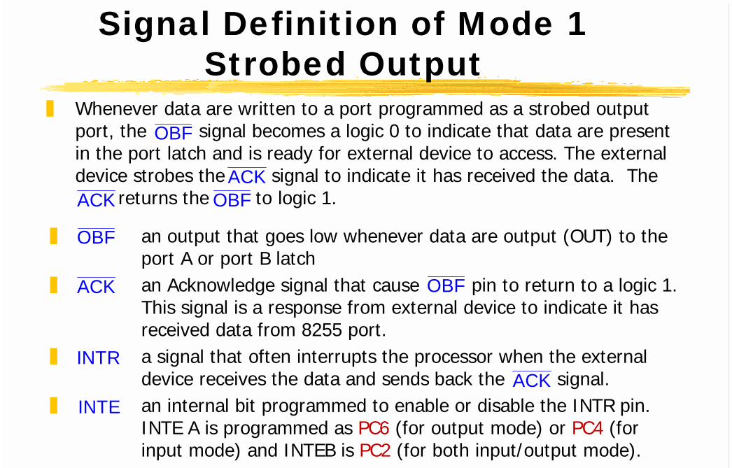
Signal Definition of Mode 1Strobed Output
Whenever data are written to a port programmed as a strobed outputport, the signal becomes a logic 0 to indicate that data are presentin the port latch and is ready for external device to access. The externaldevice strobes the signal to indicate it has received the data. The
returns the to logic 1.
an output that goes low whenever data are output (OUT) to theport A or port B latch
an Acknowledge signal that cause pin to return to a logic 1.This signal is a response from external device to indicate it hasreceived data from 8255 port.
a signal that often interrupts the processor when the externaldevice receives the data and sends back the signal.
an internal bit programmed to enable or disable the INTR pin.INTE A is programmed as PC6 (for output mode) or PC4 (forinput mode) and INTEB is PC2 (for both input/output mode).
OBF
ACK OBF
INTRACK
INTE
OBF
ACKACK OBF
ELE3230 - Chapter 12 30
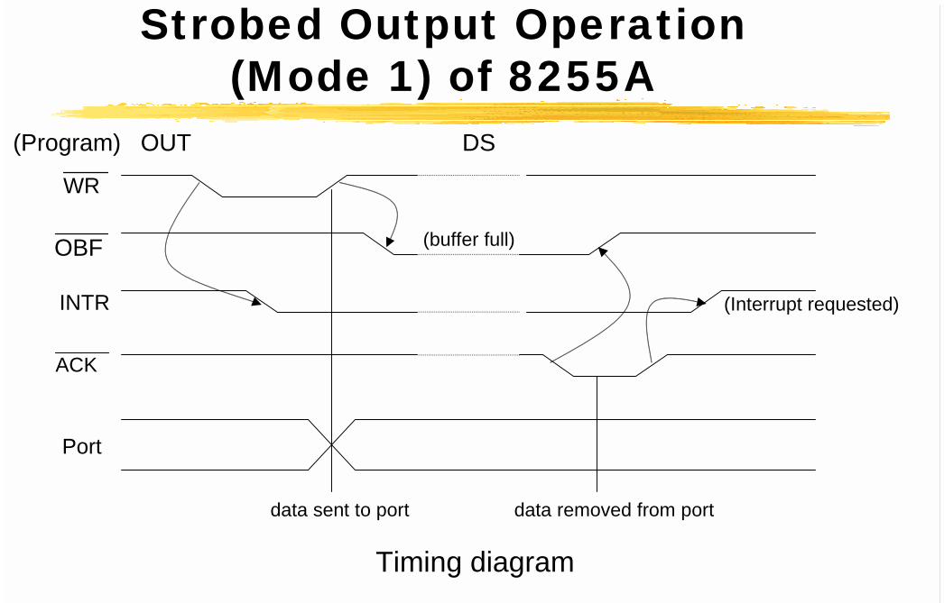
Strobed Output Operation(Mode 1) of 8255A
Timing diagram
data sent to port data removed from port
(Interrupt requested)
(buffer full)
INTR
Port
OBF
ACK
WR
(Program) OUT DS
ELE3230 - Chapter 12 31
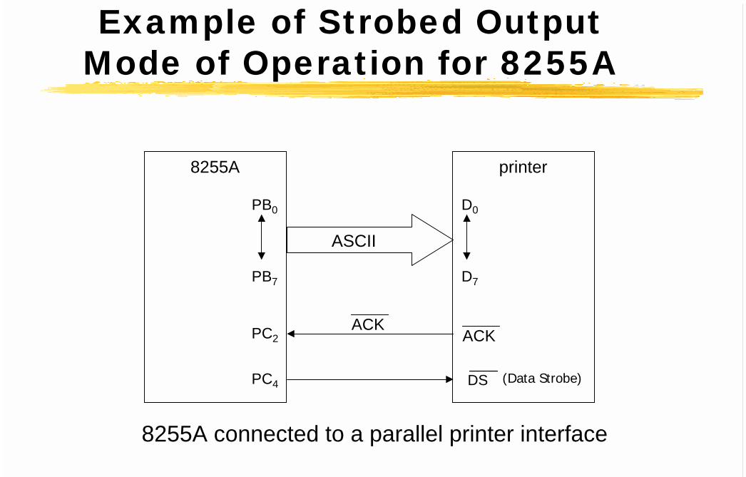
Example of Strobed OutputMode of Operation for 8255A
8255A connected to a parallel printer interface
printer
D0
D7
8255A
PC4
PC2
PB0
PB7
ASCII
ACK
DS
ACK
(Data Strobe)
ELE3230 - Chapter 12 33
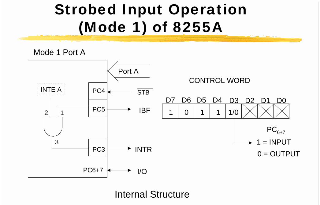
Strobed Input Operation(Mode 1) of 8255A
Internal Structure
Mode 1 Port A
Port A
INTE A
12
3
PC6+7
PC5
PC4
PC3
IBF
INTR
I/O
STBD6 D5 D4 D3D7 D2 D1 D0
11 1/01 0
CONTROL WORD
PC6+7
1 = INPUT0 = OUTPUT
ELE3230 - Chapter 12 34
Strobed Input Operation(Mode 1) of 8255A
Internal Structure
Mode 1 Port B
Port B
INTE B
45
6
PC1
PC2
PC0
IBF
INTR
STB
D6 D5 D4 D3D7 D2 D1 D0111
CONTROL WORD
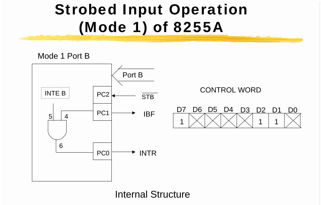
ELE3230 - Chapter 12 35
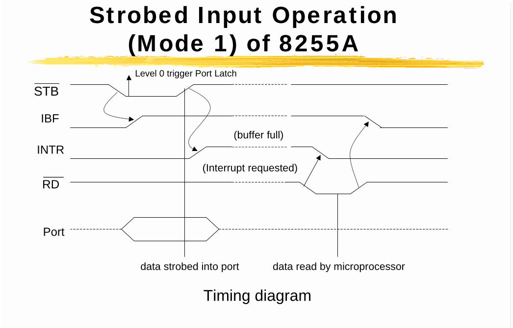
Strobed Input Operation(Mode 1) of 8255A
Timing diagram
data strobed into port data read by microprocessor
(Interrupt requested)
(buffer full)IBF
INTR
Port
STB
RD
Level 0 trigger Port Latch
ELE3230 - Chapter 12 41
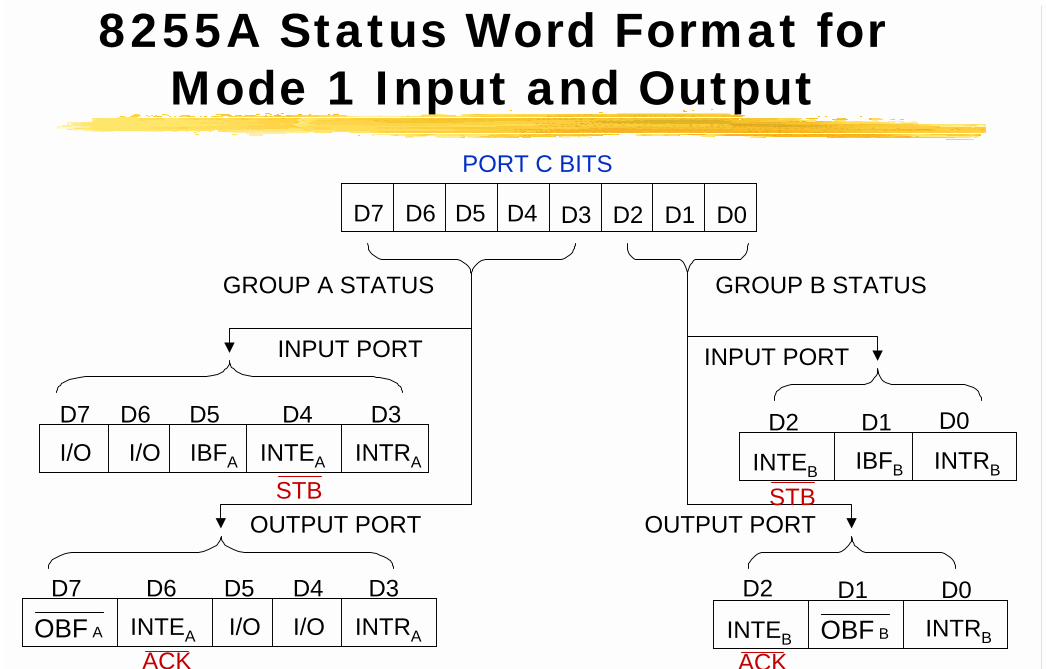
8255A Status Word Format forMode 1 Input and Output
D6 D5 D4 D3 D2 D1 D0D7I/O I/O
I/O I/O INTRB
INTRA
AOBF
IBFA INTEA INTRB
INTRAINTEA INTEB
INTEB
BOBF
IBFB
D6 D5 D4 D3D7
D6 D5 D4 D3D7
D2 D1 D0
D2 D1 D0
PORT C BITS
GROUP A STATUS GROUP B STATUS
OUTPUT PORT
INPUT PORT
OUTPUT PORT
INPUT PORT
STBSTB
ACKACK
ELE3230 - Chapter 12 42
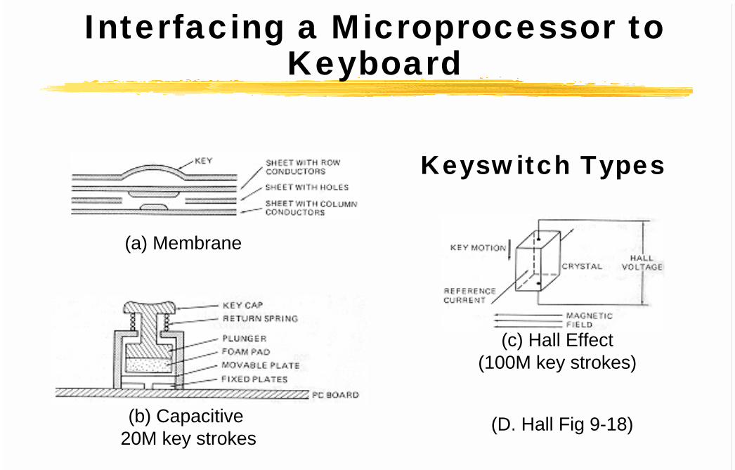
Keyswitch Types
(a) Membrane
(b) Capacitive 20M key strokes
(c) Hall Effect(100M key strokes)
(D. Hall Fig 9-18)
Interfacing a Microprocessor toKeyboard
ELE3230 - Chapter 12 43
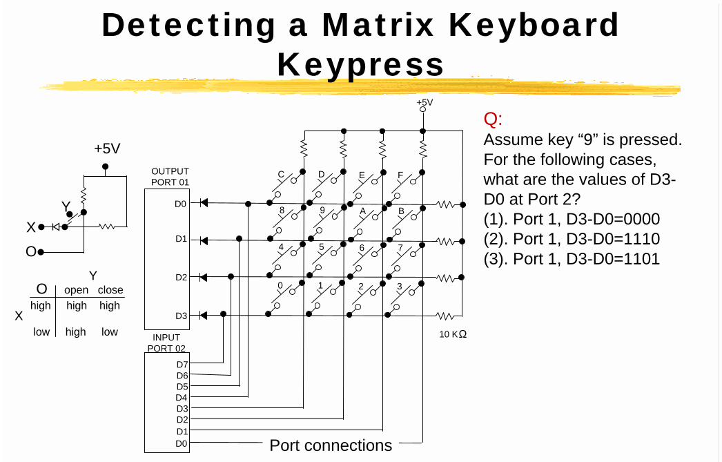
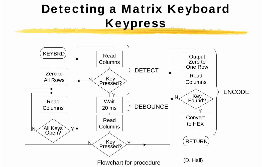
Detecting a Matrix KeyboardKeypress
C
Port connections
D E F
8 9 A B
4 5 6 7
0 1 2 3
OUTPUTPORT 01
INPUTPORT 02
D0
D1
D2
D3
D7D6D5D4D3D2D1D0
10 KΩ
+5V
Q:Assume key “9” is pressed.For the following cases,what are the values of D3-D0 at Port 2?(1). Port 1, D3-D0=0000(2). Port 1, D3-D0=1110(3). Port 1, D3-D0=1101
XO
Y
+5V
open closehigh high high
low high low
Y
X
O
ELE3230 - Chapter 12 44
Detecting a Matrix KeyboardKeypress
Flowchart for procedure
KEYBRD ReadColumns
Zero toAll Rows
All KeysOpen?
Y
N
ReadColumns
KeyPressed?
ReadColumns
Wait20 ms
KeyFound?
RETURN
Convertto HEX
KeyPressed?
ReadColumns
OutputZero to
One Row
Y
Y
Y
N
N
N
DETECT
DEBOUNCE
ENCODE
(D. Hall)
ELE3230 - Chapter 12 51
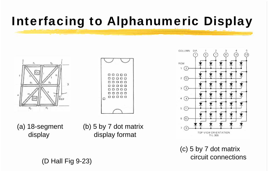
Interfacing to Alphanumeric Display
(a) 18-segment display
(b) 5 by 7 dot matrix display format
(c) 5 by 7 dot matrix circuit connections(D Hall Fig 9-23)
ELE3230 - Chapter 12 52
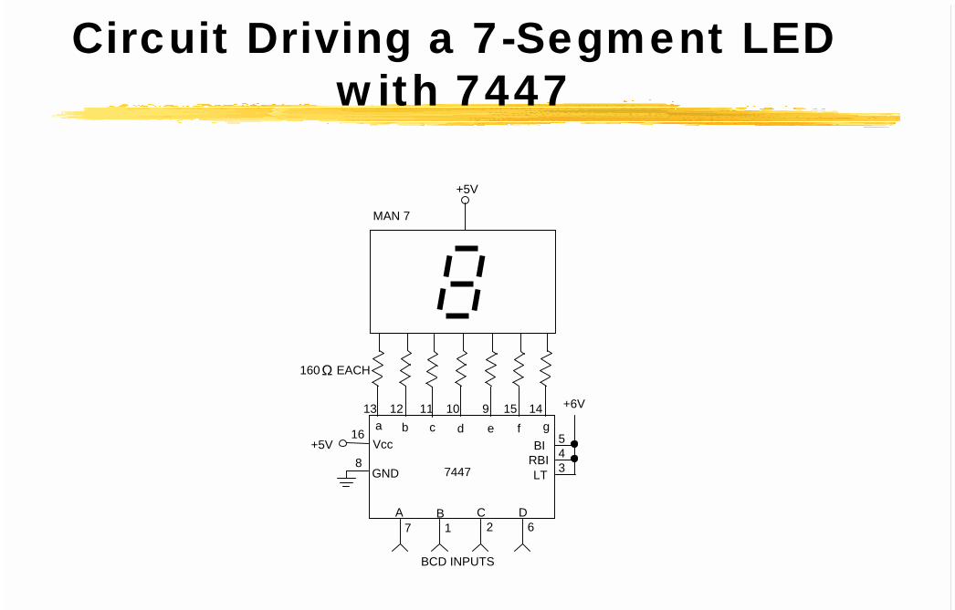
Circuit Driving a 7-Segment LEDwith 7447
160 EACHΩ
+5V
MAN 7
+5V16
8
13 12 11 10 9 15 14 +6V
a b c d e f gVcc
GND 7447
BIRBILT
543
A B C D7 1 2 6
BCD INPUTS
ELE3230 - Chapter 12 53
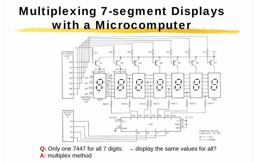
Multiplexing 7-segment Displayswith a Microcomputer
Q: Only one 7447 for all 7 digits. → display the same values for all?A: multiplex method
ELE3230 - Chapter 12 54
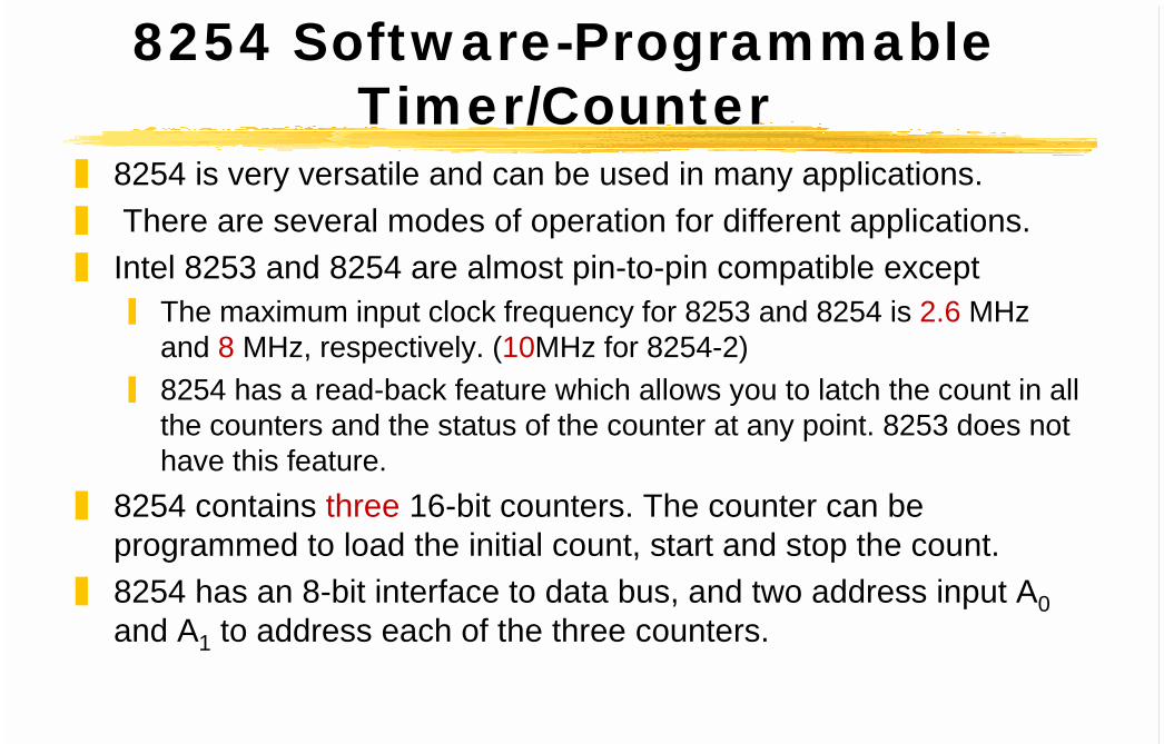
8254 Software-ProgrammableTimer/Counter
8254 is very versatile and can be used in many applications. There are several modes of operation for different applications. Intel 8253 and 8254 are almost pin-to-pin compatible except
The maximum input clock frequency for 8253 and 8254 is 2.6 MHzand 8 MHz, respectively. (10MHz for 8254-2)
8254 has a read-back feature which allows you to latch the count in allthe counters and the status of the counter at any point. 8253 does nothave this feature.
8254 contains three 16-bit counters. The counter can beprogrammed to load the initial count, start and stop the count.
8254 has an 8-bit interface to data bus, and two address input A0and A1 to address each of the three counters.
ELE3230 - Chapter 12 55
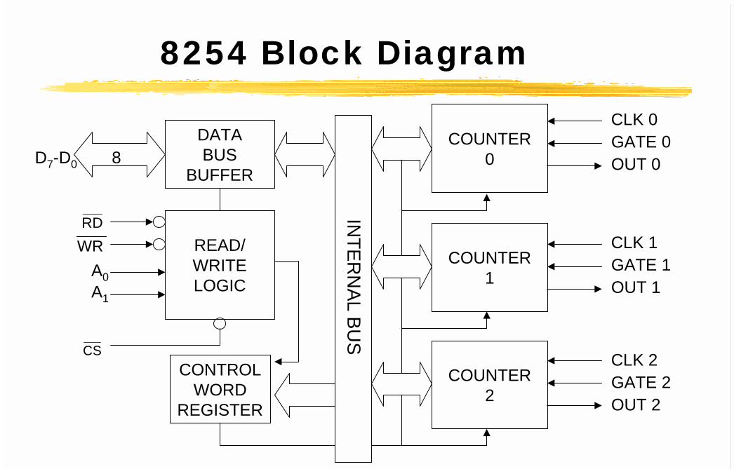
8254 Block Diagram
READ/WRITELOGIC
CONTROLWORD
REGISTER
COUNTER0
COUNTER1
COUNTER2
DATABUS
BUFFER
INTER
NAL BU
S
8D7-D0
CLK 1GATE 1OUT 1
CLK 2GATE 2OUT 2
CLK 0GATE 0OUT 0
A1
A0
RDWR
CS
ELE3230 - Chapter 12 56
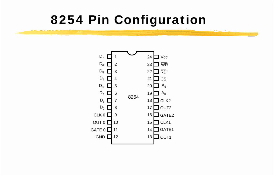
8254 Pin Configuration
2
24
23
2221
20
191817
16
15
14
131211
10
9
87
6
5
43
1
8254
Vcc
WR
RDCSA1
A0
CLK2
OUT2
GATE2CLK1
GATE1
OUT1
D7
D6
D5
D4
D3
D2
D1
CLK 0
OUT 0
GNDGATE 0
D0
ELE3230 - Chapter 12 57
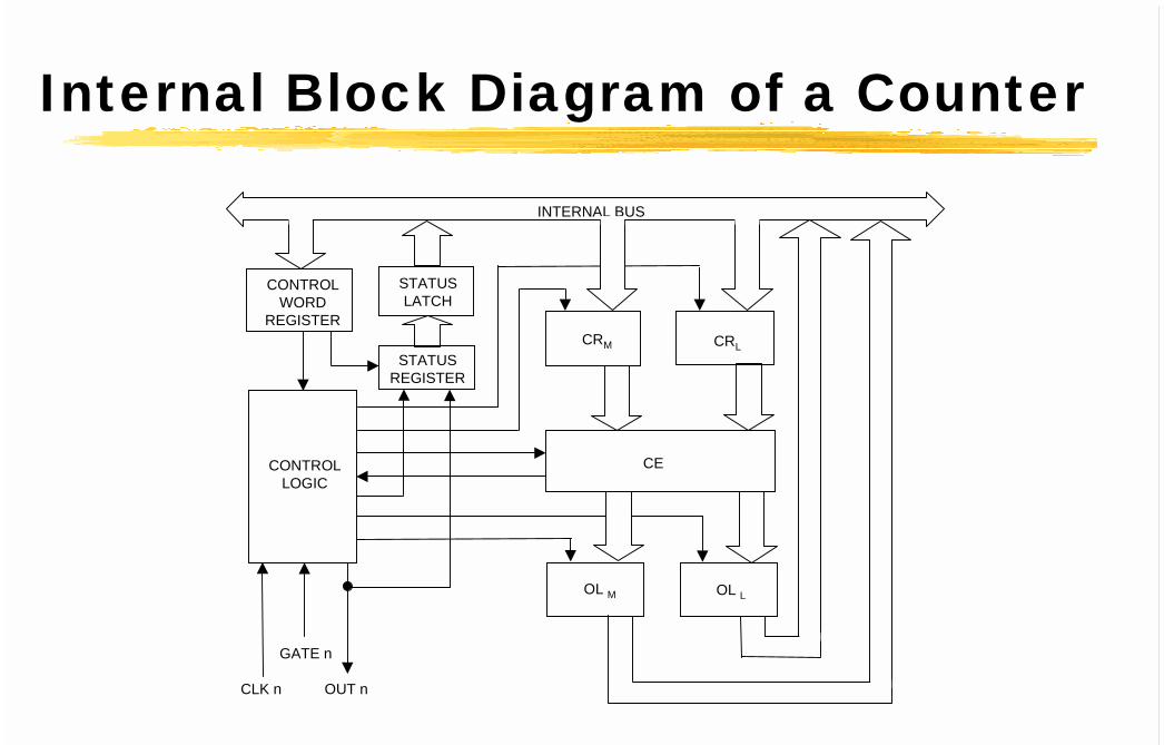
Internal Block Diagram of a Counter
INTERNAL BUS
CONTROLLOGIC
STATUSREGISTER
STATUSLATCH
CONTROLWORD
REGISTER
CE
CRM CRL
OL M OL L
GATE n
CLK n OUT n
ELE3230 - Chapter 12 58
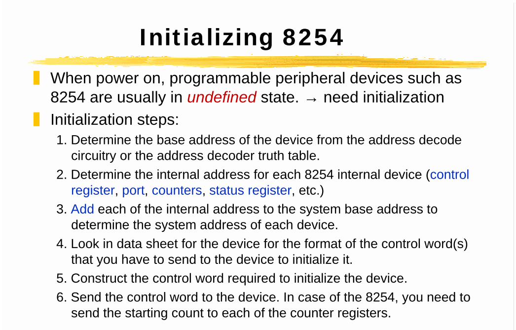
Initializing 8254 When power on, programmable peripheral devices such as
8254 are usually in undefined state. → need initialization Initialization steps:
1. Determine the base address of the device from the address decodecircuitry or the address decoder truth table.
2. Determine the internal address for each 8254 internal device (controlregister, port, counters, status register, etc.)
3. Add each of the internal address to the system base address todetermine the system address of each device.
4. Look in data sheet for the device for the format of the control word(s)that you have to send to the device to initialize it.
5. Construct the control word required to initialize the device.6. Send the control word to the device. In case of the 8254, you need to
send the starting count to each of the counter registers.
ELE3230 - Chapter 12 59
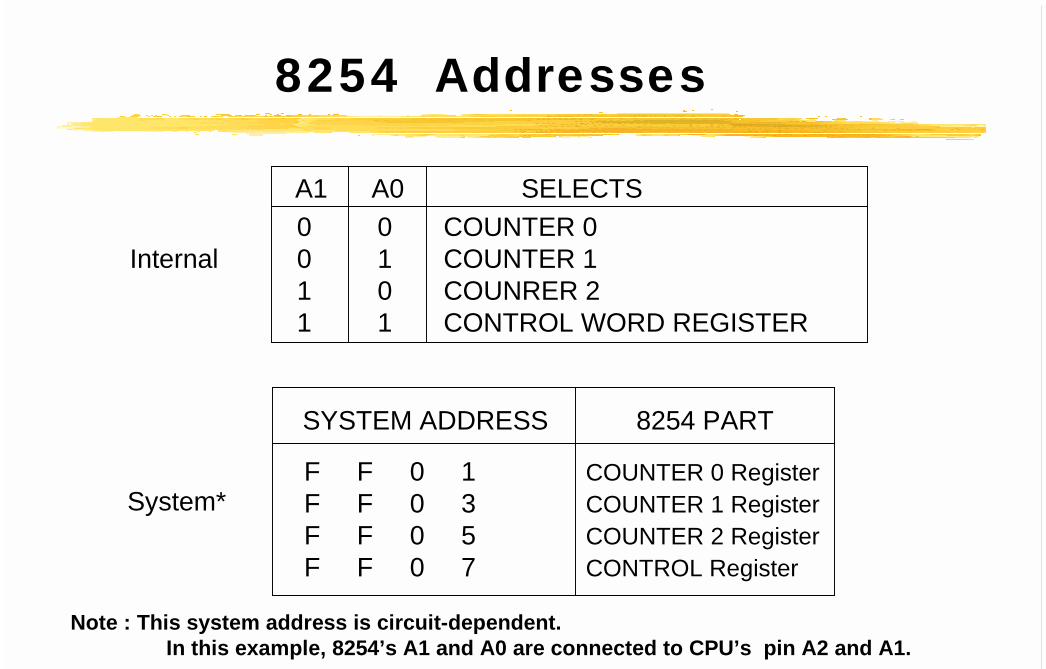
8254 Addresses
A1 A0 SELECTS0 0 COUNTER 00 1 COUNTER 11 0 COUNRER 21 1 CONTROL WORD REGISTER
Internal
SYSTEM ADDRESS 8254 PART
F F 0 1 COUNTER 0 RegisterF F 0 3 COUNTER 1 RegisterF F 0 5 COUNTER 2 RegisterF F 0 7 CONTROL Register
System*
Note : This system address is circuit-dependent. In this example, 8254’s A1 and A0 are connected to CPU’s pin A2 and A1.
ELE3230 - Chapter 12 60
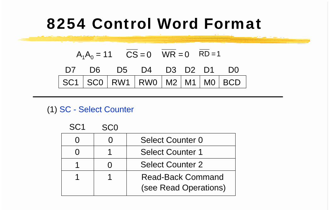
8254 Control Word Format
A1A0 = 11 0CS = 1RD =0WR =
SC1 SC0 RW1 RW0 M2 M1 M0 BCDD7 D6 D5 D4 D3 D2 D1 D0
(1) SC - Select Counter
SC1 SC00 00
011
1 1
Select Counter 1Select Counter 2
Select Counter 0
Read-Back Command(see Read Operations)
ELE3230 - Chapter 12 61
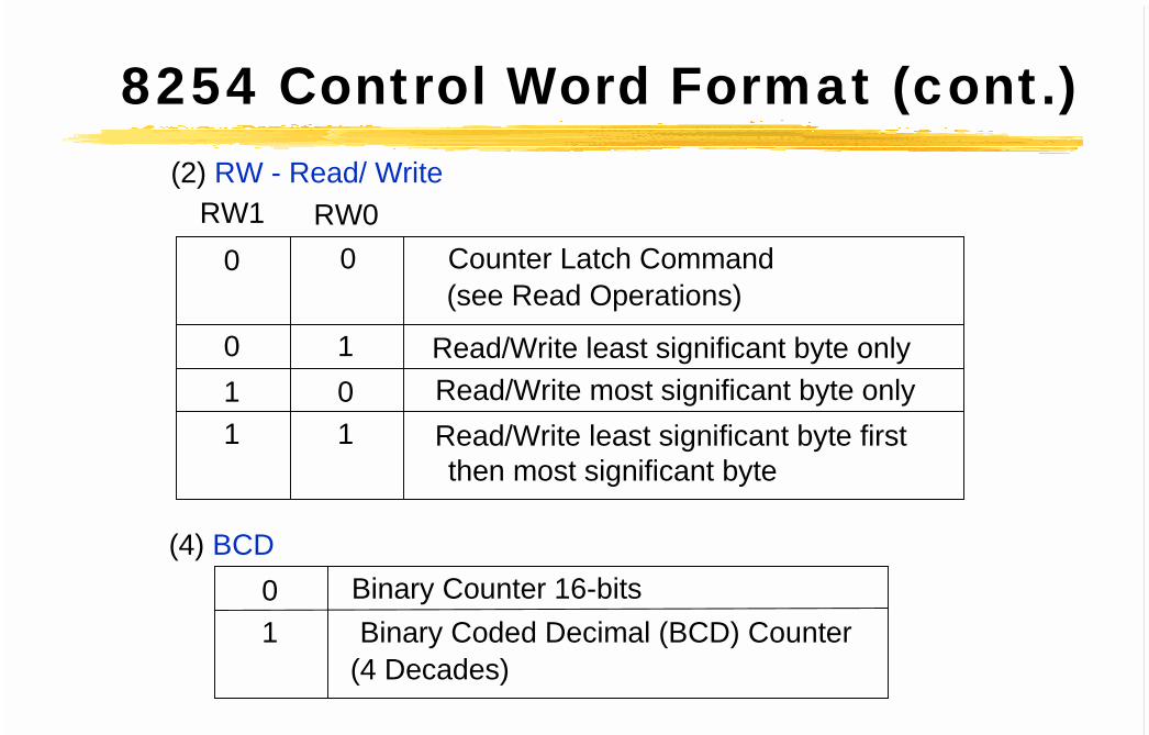
8254 Control Word Format (cont.)
RW1 RW00 0
0011
1 1
Counter Latch Command(see Read Operations)
(2) RW - Read/ Write
then most significant byteRead/Write least significant byte first
Read/Write least significant byte onlyRead/Write most significant byte only
01
Binary Counter 16-bitsBinary Coded Decimal (BCD) Counter
(4 Decades)
(4) BCD
ELE3230 - Chapter 12 62
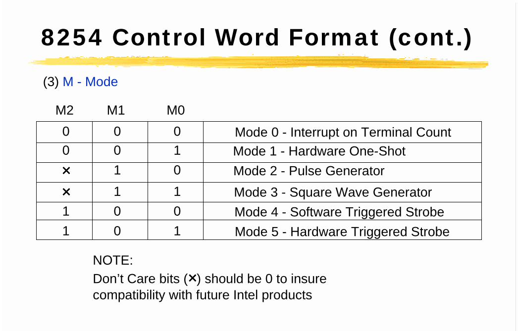
8254 Control Word Format (cont.)(3) M - Mode
M2 M1 M0
Mode 1 - Hardware One-Shot0 10Mode 2 - Pulse Generator1 0××××Mode 3 - Square Wave Generator1 1××××Mode 4 - Software Triggered Strobe0 01Mode 5 - Hardware Triggered Strobe0 11
Mode 0 - Interrupt on Terminal Count0 00
NOTE:Don’t Care bits (××××) should be 0 to insurecompatibility with future Intel products
ELE3230 - Chapter 12 64
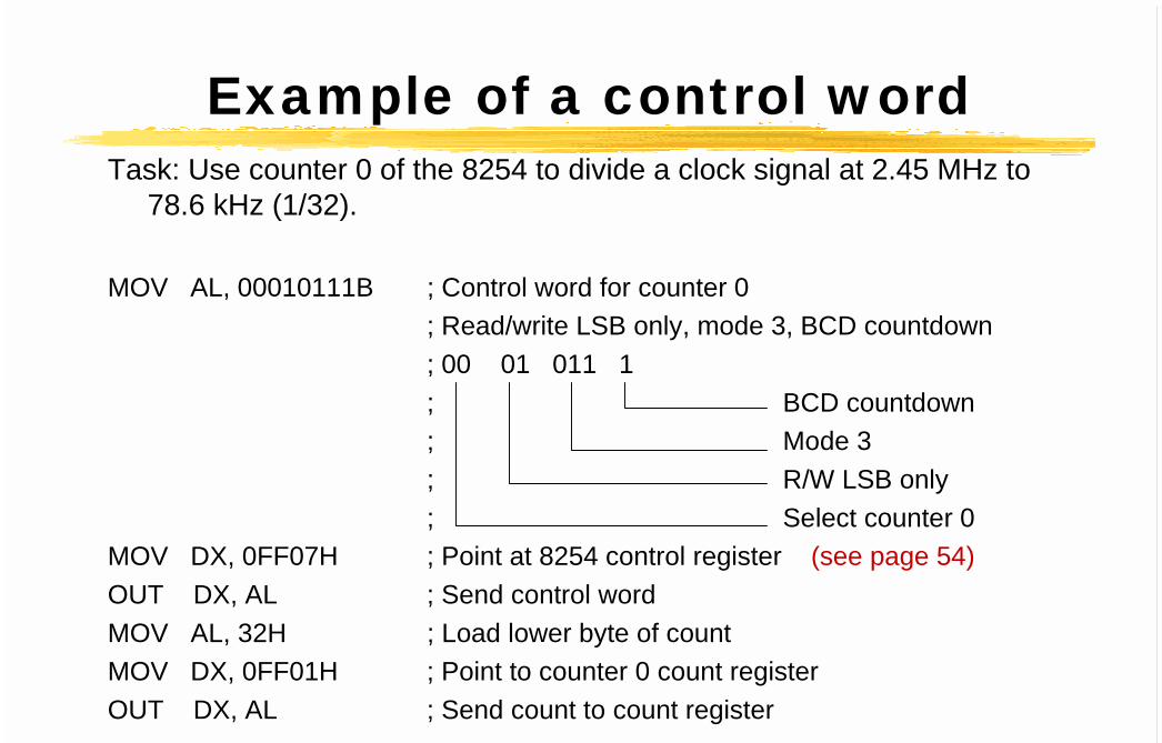
Task: Use counter 0 of the 8254 to divide a clock signal at 2.45 MHz to78.6 kHz (1/32).
MOV AL, 00010111B ; Control word for counter 0; Read/write LSB only, mode 3, BCD countdown; 00 01 011 1; BCD countdown; Mode 3; R/W LSB only; Select counter 0
MOV DX, 0FF07H ; Point at 8254 control register (see page 54)OUT DX, AL ; Send control wordMOV AL, 32H ; Load lower byte of countMOV DX, 0FF01H ; Point to counter 0 count registerOUT DX, AL ; Send count to count register
Example of a control word
ELE3230 - Chapter 12 65
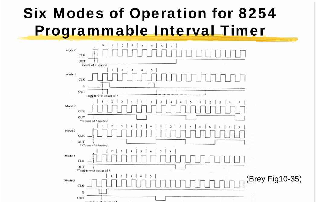
Six Modes of Operation for 8254Programmable Interval Timer
The G input stops the count when 0 in modes 2, 3 and 4
(Brey Fig10-35)
ELE3230 - Chapter 12 66
8254 Mode Operation Mode 0: Allows 8254 counter to be used as an event counter. The
output becomes a logic 0 when the control word is written and remainsuntil N plus the number of programmed counts.
Mode 1: Causes the counter to function as a retriggerable monostablemultivibrator (one shot). In this mode, the G input triggers the counter sothat it develops a pulse at the OUT connection that becomes a logic 0 forthe duration of the counter. If the count is 10, then the OUT connectiongoes low for 10 clock period when triggered. If the G input occurs withinthe duration of the output pulse, the counter is again reloaded with thecount and the OUT connection continues for the total length of the count.
Mode 2: Allows the counter to generate a series of continuous pulesthat are one clock pulse in width. The separation between pulses isdetermined by the count. (periodic pulse generator)
ELE3230 - Chapter 12 67
8254 Mode Operation (cont.)
Mode 3: Generates a continuous square-wave at the OUT connection,provided the G pin is a logic 1. If the count is even, the output is high forone-half of the count and low for one-half of the count. If the count is odd,the output is high for one clocking period longer than it is low.
Mode 4: Allows the counter to produce a single pulse at the output. Ifthe count is 10, the output is high for 10 clocking period and then low for 1clocking period. (software-triggered strobe) (Writing the count to thecounter register starts the count.)
Mode 5: A hardware triggered one-shot that functions as mode 4except that it is started by a trigger pulse on the G pin instead of bysoftware. This mode is also similar to mode 1 because it is retriggerable.(hardware-triggered strobe) (Count will be transferred to counter registerafter trigger goes high.)
Recommended


