Rev. 1.1, Date: Feb., 21, 2006
This document is issued by MediaTek Inc. in confidence and is not to be reproduced in whole or in part without the prior written permission of MediaTek Inc. and is to be used only for the purpose for which it is submitted and is not to be released in whole or in part without the prior written permission of MediaTek Inc.
Confidential Information
MediaTek Inc.
6301 Touch-Screen Controller Specifications
MediaTek
MTK Confidential A (機密)
(宇陽
聯發機密不得洩漏
MTK CONFIDENTIALNO DISCLOSURE
宇陽)Free Datasheet http://www.datasheetlist.com/
6301 TSC Specification Commercial Confidential MediaTek Inc.
Confidential Information Revision 1.1 – Feb. 21, 2006 2 / 17 © 2006 MediaTek Inc.
The information contained in this document cannot be distributed or reproduced without the prior written permission of MediaTek Inc.
1 Revised History............................................................................................................................................... 3
2 Introduction ..................................................................................................................................................... 4
3 Functional Description ................................................................................................................................... 5
3.1 General....................................................................................................................................................... 5 3.2 ADC Transfer Function ............................................................................................................................... 6 3.3 Analog Input ............................................................................................................................................... 6 3.4 Reference Input .......................................................................................................................................... 6 3.5 Control Register.......................................................................................................................................... 8 3.6 Digital Serial Interface................................................................................................................................. 8 3.7 Digital Interface Timing ............................................................................................................................. 10 3.8 Pen Interrupt Request............................................................................................................................... 10
4 Specifications................................................................................................................................................ 11
4.1 Absolute maximum over operating free-air temperature range................................................................. 11 4.2 Operating conditions................................................................................................................................. 11 4.3 Recommended operating specifications ................................................................................................... 11
5 Pin Assignment and Package ...................................................................................................................... 13
5.1 Pin Assignment......................................................................................................................................... 13 5.2 Package Information................................................................................................................................. 14 5.3 Application Example ................................................................................................................................. 16
6 Ordering Information .................................................................................................................................... 17
Table 1 Input Configurations ..................................................................................................................................................... 7 Table 2 Order of Register Bits.................................................................................................................................................... 8 Table 3 Power-Down Selection ................................................................................................................................................... 8 Table 4 Timing Specifications................................................................................................................................................... 10 Table 5 Absolute Maximum Ratings........................................................................................................................................ 11 Table 6 Operation Condition .................................................................................................................................................... 11 Table 7 General Specifications ................................................................................................................................................. 11 Table 8 Pin Assignment............................................................................................................................................................. 13
Figure 1 MT6301 Block Diagram............................................................................................................................................... 5
Figure 2 MT6301 Ideal Transfer Function................................................................................................................................ 6 Figure 3 Simplified Diagram of Single-Ended Reference Mode .............................................................................................. 7 Figure 4 Simplified Diagram of Differential Reference Mode ................................................................................................. 7 Figure 5 Conversion Timing, 24DCLKS per CONVERSION, 8-Bit Bus Interface ............................................................... 9 Figure 6 Conversion Timing, 16DCLKS per CONVERSION, 8-Bit Bus Interface ............................................................... 9 Figure 7 Conversion Timing, 15DCLKS per CONVERSION, 8-Bit Bus Interface ............................................................... 9 Figure 8 Timing Diagram ......................................................................................................................................................... 10 Figure 9 Application Example .................................................................................................................................................. 16
MTK Confidential A (機密)
(宇陽
聯發機密不得洩漏
MTK CONFIDENTIALNO DISCLOSURE
宇陽)Free Datasheet http://www.datasheetlist.com/
6301 TSC Specification Commercial Confidential MediaTek Inc.
Confidential Information Revision 1.1 – Feb. 21, 2006 3 / 17 © 2006 MediaTek Inc.
The information contained in this document cannot be distributed or reproduced without the prior written permission of MediaTek Inc.
1 Revised History
Version Data Prepared by Note
Ver. 1.0 Feb. 15 2006 HI Chen First Release
Ver. 1.1 Feb. 21 2006 HI Chen Define Pin Assignments
MTK Confidential A (機密)
(宇陽
聯發機密不得洩漏
MTK CONFIDENTIALNO DISCLOSURE
宇陽)Free Datasheet http://www.datasheetlist.com/

6301 TSC Specification Commercial Confidential MediaTek Inc.
Confidential Information Revision 1.1 – Feb. 21, 2006 4 / 17 © 2006 MediaTek Inc.
The information contained in this document cannot be distributed or reproduced without the prior written permission of MediaTek Inc.
2 Introduction
The MT6301 Touch-Screen Controller IC is a 12-bit successive approximation ADC with synchronous serial interface and low on resistance drivers for 4-wire resistive touch screens. MT6301 operates from a single 2.6V to 5.5V power supply and dissipate typical 700uW power at 125 KHz throughput rate and a 2.8V supply. The reference voltage can be varied from 1V to Vdd, while the analog input range is from 0V to Vref. The supply current is below 1uA at power-down mode. With the proprietary power-saving technique, the ON time of the driver switches could be shorten to alleviate power dissipation on the touch screen device in ratio-metric conversion operation. It is especially benefic when the sampling rate is high. With the low power, high speed, and integrated driver switches features, the MT6301 is ideal for battery-operated portable equipments such as mobile cellular phones, personal digital assistants with resistive touch screen features. The MT6301 is provided in a TSSOP-16 and QFN-16 packages and operated over wide temperature range.
MTK Confidential A (機密)
(宇陽
聯發機密不得洩漏
MTK CONFIDENTIALNO DISCLOSURE
宇陽)Free Datasheet http://www.datasheetlist.com/
6301 TSC Specification Commercial Confidential MediaTek Inc.
Confidential Information Revision 1.1 – Feb. 21, 2006 5 / 17 © 2006 MediaTek Inc.
The information contained in this document cannot be distributed or reproduced without the prior written permission of MediaTek Inc.
3 Functional Description
3.1 General
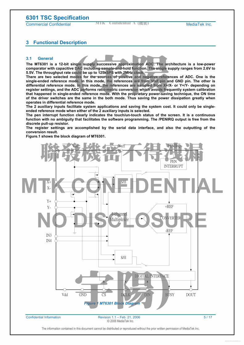
The MT6301 is a 12-bit single supply successive approximation ADC. The architecture is a low-power comparator with capacitive DAC including sample-and-hold function. The single supply ranges from 2.6V to 5.5V. The throughput rate could be up to 125kSPS with 2MHz clock. There are two selected modes for the sources of positive and negative references of ADC. One is the single-ended reference mode. In this mode, the references are from Vref pin and GND pin. The other is differential reference mode. In this mode, the references are sampled from X+/X- or Y+/Y- depending on register settings, and the ADC performs ratio-metric conversion which avoids frequently system calibration that happened in single-ended reference mode. With the proprietary power-saving technique, the ON time of the driver switches are the same in the both mode. Thus saving the power dissipation greatly when operates in differential reference mode. The 2 auxiliary inputs facilitate system applications and saving the system cost. It could only be single-ended reference mode when either of the 2 auxiliary inputs is selected. The pen interrupt function clearly indicates the touch/un-touch status of the screen. It is a continuous function with no ambiguity that facilitates the software programming. The /PENIRQ output is free from the discrete pull-up resistor. The register settings are accomplished by the serial data interface, and also the outputting of the conversion result. Figure.1 shows the block diagram of MT6301.
4-channel
Multiplexer CONVERTER
S/H
S/H
+REF
-REF
PEN
INTERRUPT
DIGITAL INTERFACE
PENIRQVrefVdd
X+
X-
Y+
Y-
IN3
IN4
Vdd GND DOUTBUSYDINDCLKCS
Figure 1 MT6301 Block Diagram
MTK Confidential A (機密)
(宇陽
聯發機密不得洩漏
MTK CONFIDENTIALNO DISCLOSURE
宇陽)Free Datasheet http://www.datasheetlist.com/
6301 TSC Specification Commercial Confidential MediaTek Inc.
Confidential Information Revision 1.1 – Feb. 21, 2006 6 / 17 © 2006 MediaTek Inc.
The information contained in this document cannot be distributed or reproduced without the prior written permission of MediaTek Inc.
3.2 ADC Transfer Function
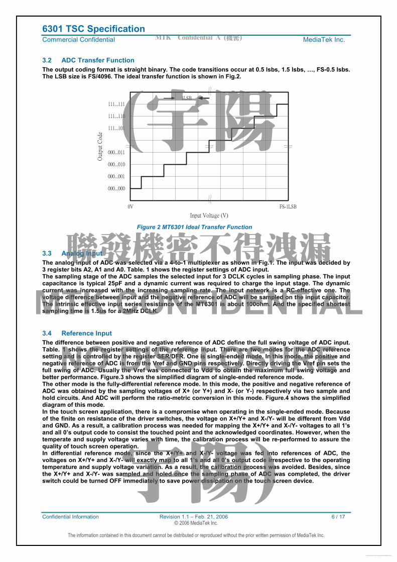
The output coding format is straight binary. The code transitions occur at 0.5 lsbs, 1.5 lsbs, …, FS-0.5 lsbs. The LSB size is FS/4096. The ideal transfer function is shown in Fig.2.
0V FS-1LSB
000...000
000...001
000...010
000...011
111...111
111...110
111...101
1LSB
Input Voltage (V)
Outp
ut
Code
Figure 2 MT6301 Ideal Transfer Function
3.3 Analog Input
The analog input of ADC was selected via a 4-to-1 multiplexer as shown in Fig.1. The input was decided by 3 register bits A2, A1 and A0. Table. 1 shows the register settings of ADC input. The sampling stage of the ADC samples the selected input for 3 DCLK cycles in sampling phase. The input capacitance is typical 25pF and a dynamic current was required to charge the input stage. The dynamic current was increased with the increasing sampling rate. The input network is a RC-effective one. The voltage difference between input and the negative reference of ADC will be sampled on the input capacitor. The intrinsic effective input series resistance of the MT6301 is about 100ohm. And the specified shortest sampling time is 1.5us for a 2MHz DCLK.
3.4 Reference Input
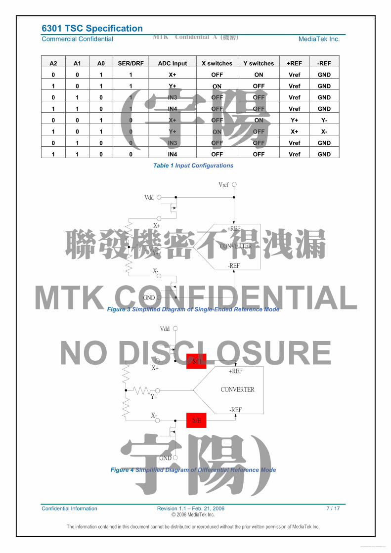
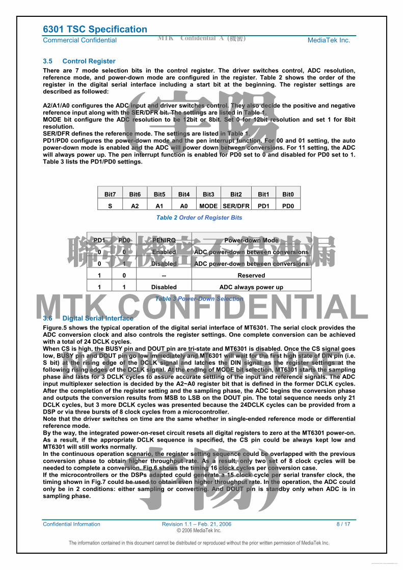
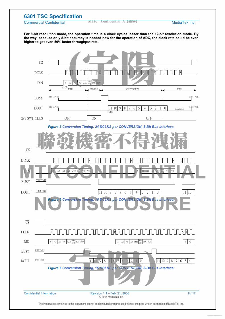
The difference between positive and negative reference of ADC define the full swing voltage of ADC input. Table. 1 shows the register settings of the reference input. There are two modes for the ADC reference setting and is controlled by the register SER/DFR. One is single-ended mode. In this mode, the positive and negative reference of ADC is from the Vref and GND pins respectively. Directly driving the Vref pin sets the full swing of ADC. Usually the Vref was connected to Vdd to obtain the maximum full swing voltage and better performance. Figure.3 shows the simplified diagram of single-ended reference mode. The other mode is the fully-differential reference mode. In this mode, the positive and negative reference of ADC was obtained by the sampling voltages of X+ (or Y+) and X- (or Y-) respectively via two sample and hold circuits. And ADC will perform the ratio-metric conversion in this mode. Figure.4 shows the simplified diagram of this mode. In the touch screen application, there is a compromise when operating in the single-ended mode. Because of the finite on resistance of the driver switches, the voltage on X+/Y+ and X-/Y- will be different from Vdd and GND. As a result, a calibration process was needed for mapping the X+/Y+ and X-/Y- voltages to all 1’s and all 0’s output code to consist the touched point and the acknowledged coordinates. However, when the temperate and supply voltage varies with time, the calibration process will be re-performed to assure the quality of touch screen operation. In differential reference mode, since the X+/Y+ and X-/Y- voltage was fed into references of ADC, the voltages on X+/Y+ and X-/Y- will exactly map to all 1’s and all 0’s output code irrespective to the operating temperature and supply voltage variation. As a result, the calibration process was avoided. Besides, since the X+/Y+ and X-/Y- was sampled and holed once the sampling phase of ADC was completed, the driver switch could be turned OFF immediately to save power dissipation on the touch screen device.
MTK Confidential A (機密)
(宇陽
聯發機密不得洩漏
MTK CONFIDENTIALNO DISCLOSURE
宇陽)Free Datasheet http://www.datasheetlist.com/
6301 TSC Specification Commercial Confidential MediaTek Inc.
Confidential Information Revision 1.1 – Feb. 21, 2006 7 / 17 © 2006 MediaTek Inc.
The information contained in this document cannot be distributed or reproduced without the prior written permission of MediaTek Inc.
A2 A1 A0 SER/DRF ADC Input X switches Y switches +REF -REF
0 0 1 1 X+ OFF ON Vref GND
1 0 1 1 Y+ ΟΝΟΝΟΝΟΝ OFF Vref GND
0 1 0 1 IN3 OFF OFF Vref GND
1 1 0 1 IN4 OFF OFF Vref GND
0 0 1 0 X+ OFF ON Y+ Y-
1 0 1 0 Y+ ΟΝΟΝΟΝΟΝ OFF X+ X-
0 1 0 0 IN3 OFF OFF Vref GND
1 1 0 0 IN4 OFF OFF Vref GND
Table 1 Input Configurations
CONVERTER
+REF
-REF
Vref
Vdd
X+
X-
Y+
GND
Figure 3 Simplified Diagram of Single-Ended Reference Mode
CONVERTER
+REF
-REF
Vdd
X+
X-
Y+
GND
S/H
S/H
Figure 4 Simplified Diagram of Differential Reference Mode
MTK Confidential A (機密)
(宇陽
聯發機密不得洩漏
MTK CONFIDENTIALNO DISCLOSURE
宇陽)Free Datasheet http://www.datasheetlist.com/
6301 TSC Specification Commercial Confidential MediaTek Inc.
Confidential Information Revision 1.1 – Feb. 21, 2006 8 / 17 © 2006 MediaTek Inc.
The information contained in this document cannot be distributed or reproduced without the prior written permission of MediaTek Inc.
3.5 Control Register
There are 7 mode selection bits in the control register. The driver switches control, ADC resolution, reference mode, and power-down mode are configured in the register. Table 2 shows the order of the register in the digital serial interface including a start bit at the beginning. The register settings are described as followed: A2/A1/A0 configures the ADC input and driver switches control. They also decide the positive and negative reference input along with the SER/DFR bit. The settings are listed in Table 1. MODE bit configure the ADC resolution to be 12bit or 8bit. Set 0 for 12bit resolution and set 1 for 8bit resolution. SER/DFR defines the reference mode. The settings are listed in Table 1. PD1/PD0 configures the power-down mode and the pen interrupt function. For 00 and 01 setting, the auto power-down mode is enabled and the ADC will power down between conversions. For 11 setting, the ADC will always power up. The pen interrupt function is enabled for PD0 set to 0 and disabled for PD0 set to 1. Table 3 lists the PD1/PD0 settings.
Bit7 Bit6 Bit5 Bit4 Bit3 Bit2 Bit1 Bit0
S A2 A1 A0 MODE SER/DFR PD1 PD0
Table 2 Order of Register Bits
PD1 PD0 PENIRQ Power-down Mode
0 0 Enabled ADC power-down between conversions
0 1 Disabled ADC power-down between conversions
1 0 -- Reserved
1 1 Disabled ADC always power up
Table 3 Power-Down Selection
3.6 Digital Serial Interface
Figure.5 shows the typical operation of the digital serial interface of MT6301. The serial clock provides the ADC conversion clock and also controls the register settings. One complete conversion can be achieved with a total of 24 DCLK cycles. When CS is high, the BUSY pin and DOUT pin are tri-state and MT6301 is disabled. Once the CS signal goes low, BUSY pin and DOUT pin go low immediately and MT6301 will wait for the first high state of DIN pin (i.e. S bit) at the rising edge of the DCLK signal and latches the DIN signal as the register settings at the following rising edges of the DCLK signal. At the ending of MODE bit selection, MT6301 starts the sampling phase and lasts for 3 DCLK cycles to assure accurate settling of the input and reference signals. The ADC input multiplexer selection is decided by the A2~A0 register bit that is defined in the former DCLK cycles. After the completion of the register setting and the sampling phase, the ADC begins the conversion phase and outputs the conversion results from MSB to LSB on the DOUT pin. The total sequence needs only 21 DCLK cycles, but 3 more DCLK cycles was presented because the 24DCLK cycles can be provided from a DSP or via three bursts of 8 clock cycles from a microcontroller. Note that the driver switches on time are the same whether in single-ended reference mode or differential reference mode. By the way, the integrated power-on-reset circuit resets all digital registers to zero at the MT6301 power-on. As a result, if the appropriate DCLK sequence is specified, the CS pin could be always kept low and MT6301 will still works normally. In the continuous operation scenario, the register setting sequence could be overlapped with the previous conversion phase to obtain higher throughput rate. As a result, only two set of 8 clock cycles will be needed to complete a conversion. Fig.6 shows the timing 16 clock cycles per conversion case. If the microcontrollers or the DSPs adapted could generate a 15 clock cycle per serial transfer clock, the timing shown in Fig.7 could be used to obtain even higher throughput rate. In the operation, the ADC could only be in 2 conditions: either sampling or converting. And DOUT pin is standby only when ADC is in sampling phase.
MTK Confidential A (機密)
(宇陽
聯發機密不得洩漏
MTK CONFIDENTIALNO DISCLOSURE
宇陽)Free Datasheet http://www.datasheetlist.com/
6301 TSC Specification Commercial Confidential MediaTek Inc.
Confidential Information Revision 1.1 – Feb. 21, 2006 9 / 17 © 2006 MediaTek Inc.
The information contained in this document cannot be distributed or reproduced without the prior written permission of MediaTek Inc.
For 8-bit resolution mode, the operation time is 4 clock cycles lesser than the 12-bit resolution mode. By the way, because only 8-bit accuracy is needed now for the operation of ADC, the clock rate could be even higher to get even 50% faster throughput rate.
1 8 1 8 1 8
S A2 A1 A0 MODESER/
DFRPD1 PD0
(START)
IDLE SMAPLE CONVERSION IDLE
TRI-STATE TRI-STATE
TRI-STATE TRI-STATE11
(MSB)
10 9 8 7 6 5 4 3 2 1 0
OFF ON OFF
Zero-Filled
CS
DCLK
DIN
BUSY
DOUT
X/Y SWITCHES
Figure 5 Conversion Timing, 24 DCLKS per CONVERSION, 8-Bit Bus Interface.
1 8 1 8 1 8
S A2 A1 A0 MODESER/
DFRPD1 PD0
TRI-STATE
TRI-STATE11 10 9 8 7 6 5 4 3 2 1 0
CS
DCLK
DIN
BUSY
DOUT
1
S A2 A1 A0 MODESER/
DFRPD1 PD0
11 10
Figure 6 Conversion Timing, 16 DCLKS per CONVERSION, 8-Bit Bus Interface.
1
S A2 A1 A0 MODESER/
DFRPD1 PD0
TRI-STATE
TRI-STATE11 10 9 8 7 6 5 4 3 2 1 0
CS
DCLK
DIN
BUSY
DOUT
S A2 A1 A0 MODESER/
DFRPD1 PD0
15 1 15 1
S A2
11 10 9 8 7 6 5 4
Figure 7 Conversion Timing, 15 DCLKS per CONVERSION, 8-Bit Bus Interface.
MTK Confidential A (機密)
(宇陽
聯發機密不得洩漏
MTK CONFIDENTIALNO DISCLOSURE
宇陽)Free Datasheet http://www.datasheetlist.com/
6301 TSC Specification Commercial Confidential MediaTek Inc.
Confidential Information Revision 1.1 – Feb. 21, 2006 10 / 17 © 2006 MediaTek Inc.
The information contained in this document cannot be distributed or reproduced without the prior written permission of MediaTek Inc.
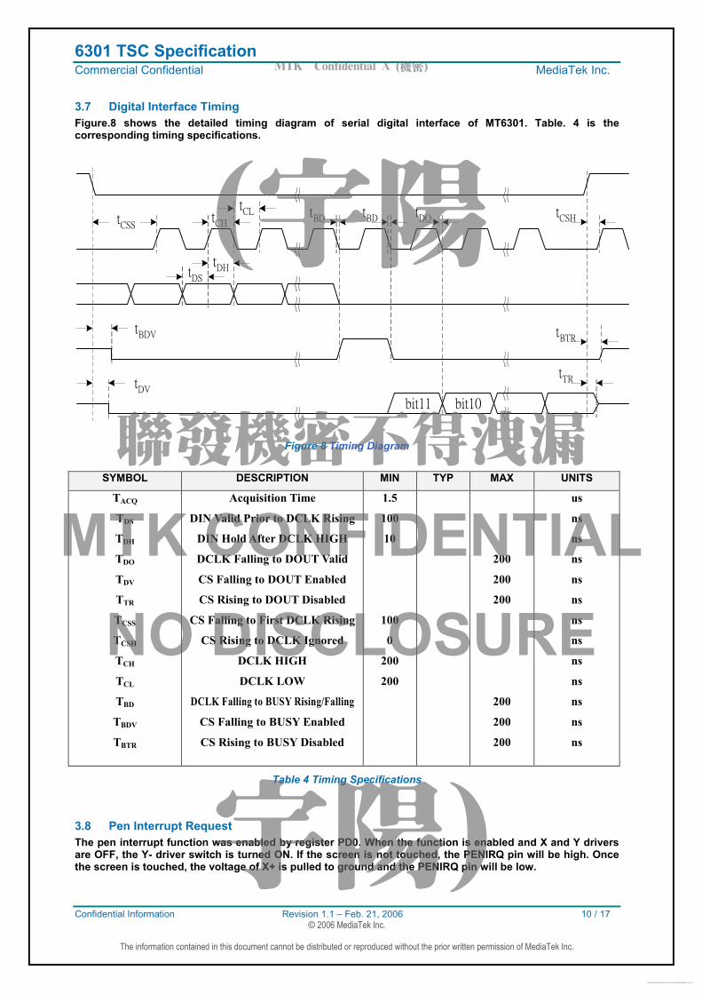
3.7 Digital Interface Timing
Figure.8 shows the detailed timing diagram of serial digital interface of MT6301. Table. 4 is the corresponding timing specifications.
tBDV
tDV
tCSS
tCH
tCL t
BDtBD
tDO
tCSH
tDS
tDH
tBTR
tTR
bit11 bit10
Figure 8 Timing Diagram
SYMBOL DESCRIPTION MIN TYP MAX UNITS
TACQ
TDS
TDH
TDO
TDV
TTR
TCSS
TCSH
TCH
TCL
TBD
TBDV
TBTR
Acquisition Time
DIN Valid Prior to DCLK Rising
DIN Hold After DCLK HIGH
DCLK Falling to DOUT Valid
CS Falling to DOUT Enabled
CS Rising to DOUT Disabled
CS Falling to First DCLK Rising
CS Rising to DCLK Ignored
DCLK HIGH
DCLK LOW
DCLK Falling to BUSY Rising/Falling
CS Falling to BUSY Enabled
CS Rising to BUSY Disabled
1.5
100
10
100
0
200
200
200
200
200
200
200
200
us
ns
ns
ns
ns
ns
ns
ns
ns
ns
ns
ns
ns
Table 4 Timing Specifications
3.8 Pen Interrupt Request
The pen interrupt function was enabled by register PD0. When the function is enabled and X and Y drivers are OFF, the Y- driver switch is turned ON. If the screen is not touched, the PENIRQ pin will be high. Once the screen is touched, the voltage of X+ is pulled to ground and the PENIRQ pin will be low.
MTK Confidential A (機密)
(宇陽
聯發機密不得洩漏
MTK CONFIDENTIALNO DISCLOSURE
宇陽)Free Datasheet http://www.datasheetlist.com/
6301 TSC Specification Commercial Confidential MediaTek Inc.
Confidential Information Revision 1.1 – Feb. 21, 2006 11 / 17 © 2006 MediaTek Inc.
The information contained in this document cannot be distributed or reproduced without the prior written permission of MediaTek Inc.
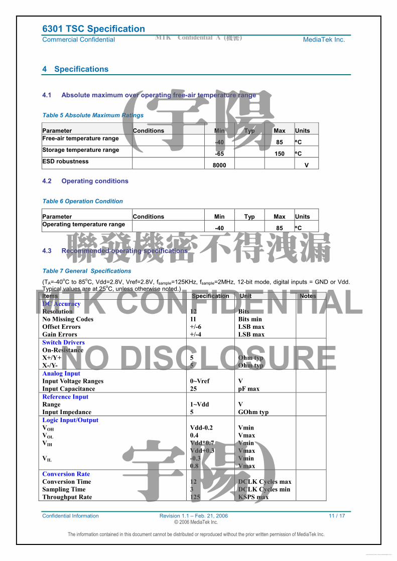
4 Specifications
4.1 Absolute maximum over operating free-air temperature range
Table 5 Absolute Maximum Ratings
Parameter Conditions Min Typ Max Units
Free-air temperature range -40 85 °°°°C
Storage temperature range -65 150 °°°°C
ESD robustness 8000 V
4.2 Operating conditions
Table 6 Operation Condition
Parameter Conditions Min Typ Max Units
Operating temperature range -40 85 °°°°C
4.3 Recommended operating specifications
Table 7 General Specifications
(TA=-40oC to 85
oC, Vdd=2.8V, Vref=2.8V, fsample=125KHz, fsample=2MHz, 12-bit mode, digital inputs = GND or Vdd.
Typical values are at 25oC, unless otherwise noted.)
Items Specification Unit Notes
DC Accuracy
Resolution
No Missing Codes
Offset Errors
Gain Errors
12
11
+/-6
+/-4
Bits
Bits min
LSB max
LSB max
Switch Drivers
On-Resistance
X+/Y+
X-/Y-
5
5
Ohm typ
Ohm typ
Analog Input
Input Voltage Ranges
Input Capacitance
0~Vref
25
V
pF max
Reference Input
Range
Input Impedance
1~Vdd
5
V
GOhm typ
Logic Input/Output
VOH VOL VIH
VIL
Vdd-0.2
0.4
Vdd*0.7
Vdd+0.3
-0.3
0.8
Vmin
Vmax
Vmin
Vmax
Vmin
Vmax
Conversion Rate
Conversion Time
Sampling Time
Throughput Rate
12
3
125
DCLK Cycles max
DCLK Cycles min
KSPS max
MTK Confidential A (機密)
(宇陽
聯發機密不得洩漏
MTK CONFIDENTIALNO DISCLOSURE
宇陽)Free Datasheet http://www.datasheetlist.com/
6301 TSC Specification Commercial Confidential MediaTek Inc.
Confidential Information Revision 1.1 – Feb. 21, 2006 12 / 17 © 2006 MediaTek Inc.
The information contained in this document cannot be distributed or reproduced without the prior written permission of MediaTek Inc.
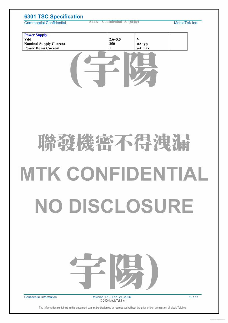
Power Supply
Vdd
Nominal Supply Current
Power Down Current
2.6~5.5
250
1
V
uA typ
uA max
MTK Confidential A (機密)
(宇陽
聯發機密不得洩漏
MTK CONFIDENTIALNO DISCLOSURE
宇陽)Free Datasheet http://www.datasheetlist.com/
6301 TSC Specification Commercial Confidential MediaTek Inc.
Confidential Information Revision 1.1 – Feb. 21, 2006 13 / 17 © 2006 MediaTek Inc.
The information contained in this document cannot be distributed or reproduced without the prior written permission of MediaTek Inc.
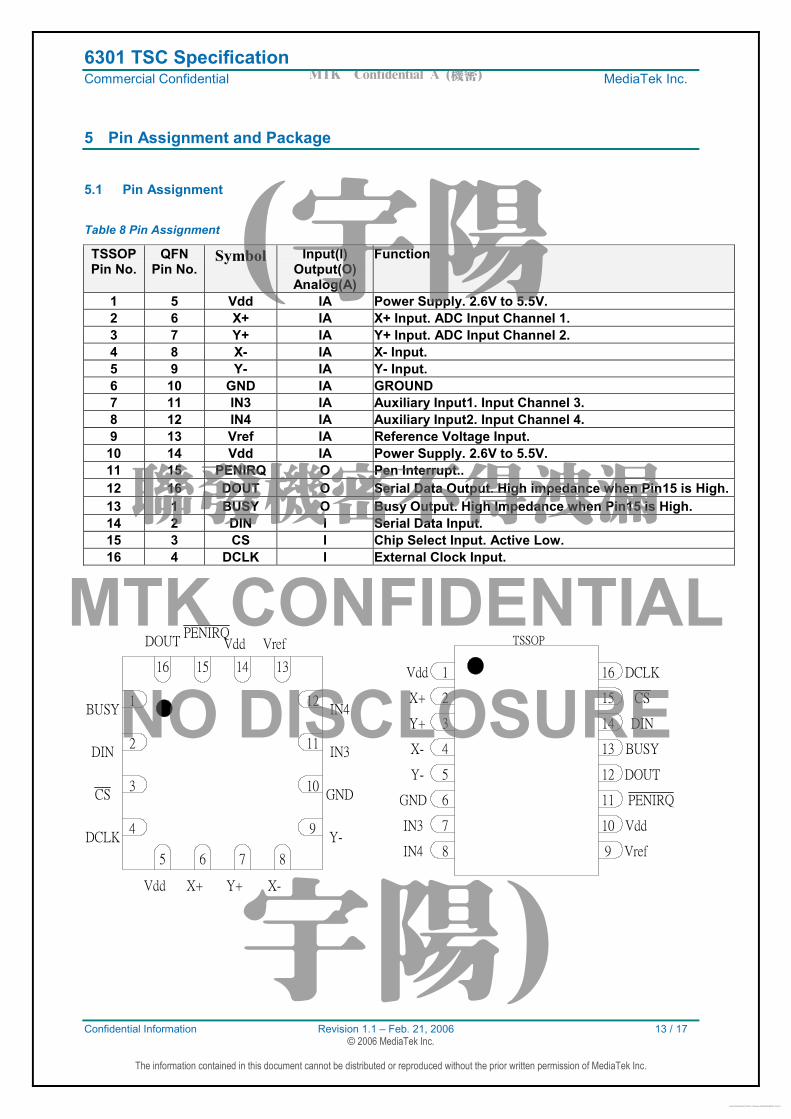
5 Pin Assignment and Package
5.1 Pin Assignment
Table 8 Pin Assignment
TSSOP Pin No.
QFN Pin No.
Symbol Input(I) Output(O) Analog(A)
Function
1 5 Vdd IA Power Supply. 2.6V to 5.5V.
2 6 X+ IA X+ Input. ADC Input Channel 1.
3 7 Y+ IA Y+ Input. ADC Input Channel 2.
4 8 X- IA X- Input.
5 9 Y- IA Y- Input.
6 10 GND IA GROUND
7 11 IN3 IA Auxiliary Input1. Input Channel 3.
8 12 IN4 IA Auxiliary Input2. Input Channel 4.
9 13 Vref IA Reference Voltage Input.
10 14 Vdd IA Power Supply. 2.6V to 5.5V.
11 15 PENIRQ O Pen Interrupt..
12 16 DOUT O Serial Data Output. High impedance when Pin15 is High.
13 1 BUSY O Busy Output. High Impedance when Pin15 is High.
14 2 DIN I Serial Data Input.
15 3 CS I Chip Select Input. Active Low.
16 4 DCLK I External Clock Input.
5 6 7 8
9
10
11
12
13141516
1
2
3
4
Vdd X+ Y+ X-
Y-
GND
IN3
IN4
VrefVddPENIRQ
DOUT
BUSY
DIN
CS
DCLK
1
2
3
4
5
6
7
8 9
10
11
12
13
14
15
16Vdd
X+
Y+
X-
Y-
GND
IN3
IN4 Vref
Vdd
DOUT
PENIRQ
BUSY
DIN
CS
DCLK
TSSOP
MTK Confidential A (機密)
(宇陽
聯發機密不得洩漏
MTK CONFIDENTIALNO DISCLOSURE
宇陽)Free Datasheet http://www.datasheetlist.com/
6301 TSC Specification Commercial Confidential MediaTek Inc.
Confidential Information Revision 1.1 – Feb. 21, 2006 14 / 17 © 2006 MediaTek Inc.
The information contained in this document cannot be distributed or reproduced without the prior written permission of MediaTek Inc.
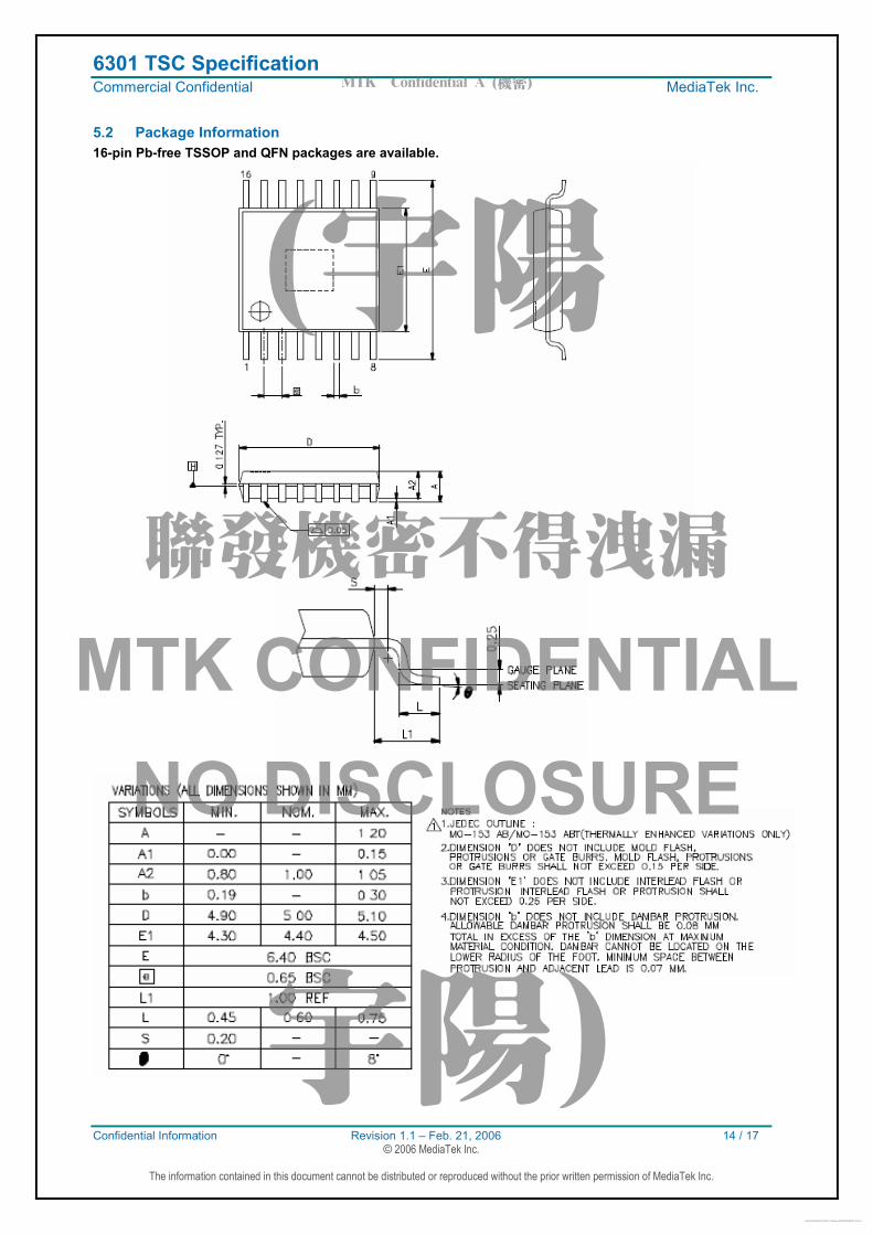
5.2 Package Information
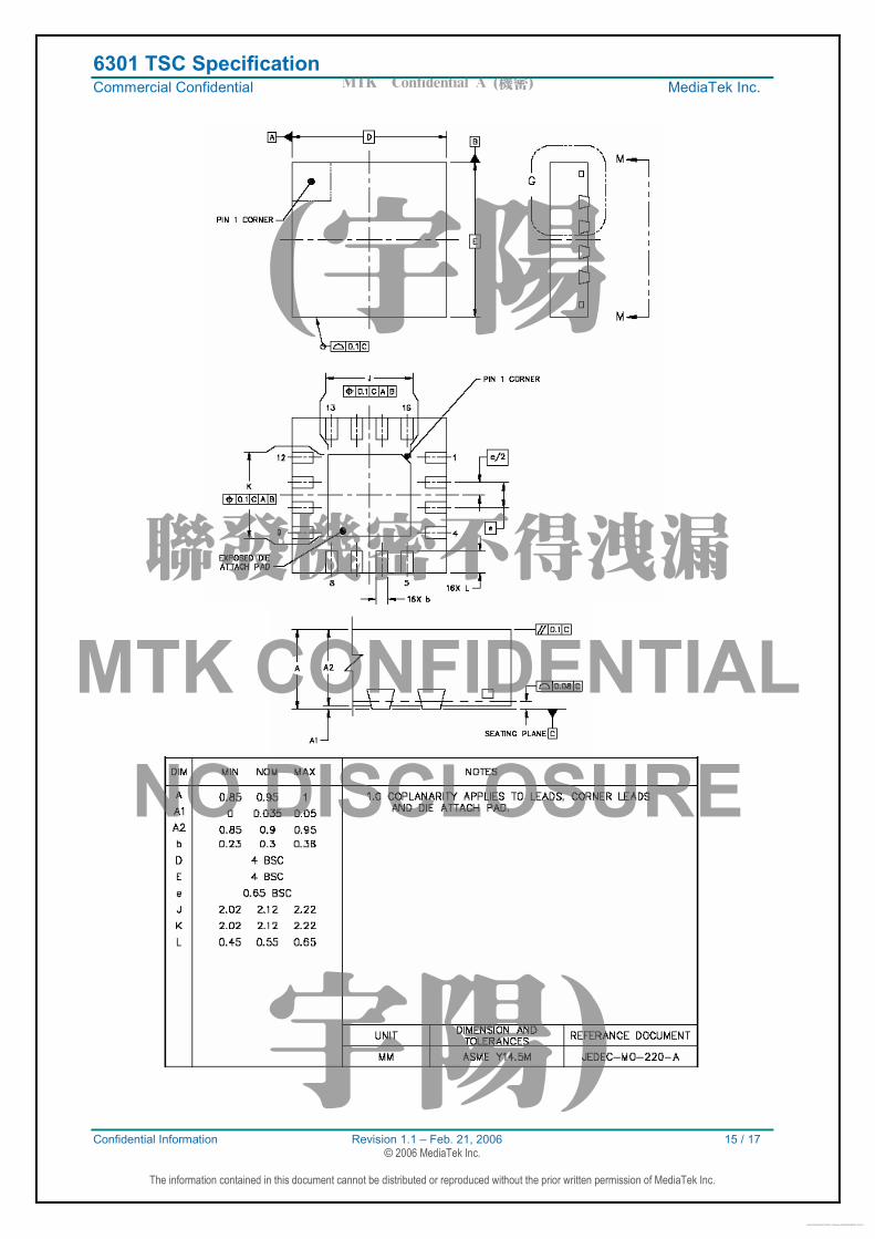
16-pin Pb-free TSSOP and QFN packages are available.
MTK Confidential A (機密)
(宇陽
聯發機密不得洩漏
MTK CONFIDENTIALNO DISCLOSURE
宇陽)Free Datasheet http://www.datasheetlist.com/
6301 TSC Specification Commercial Confidential MediaTek Inc.
Confidential Information Revision 1.1 – Feb. 21, 2006 15 / 17 © 2006 MediaTek Inc.
The information contained in this document cannot be distributed or reproduced without the prior written permission of MediaTek Inc.
MTK Confidential A (機密)
(宇陽
聯發機密不得洩漏
MTK CONFIDENTIALNO DISCLOSURE
宇陽)Free Datasheet http://www.datasheetlist.com/
6301 TSC Specification Commercial Confidential MediaTek Inc.
Confidential Information Revision 1.1 – Feb. 21, 2006 16 / 17 © 2006 MediaTek Inc.
The information contained in this document cannot be distributed or reproduced without the prior written permission of MediaTek Inc.
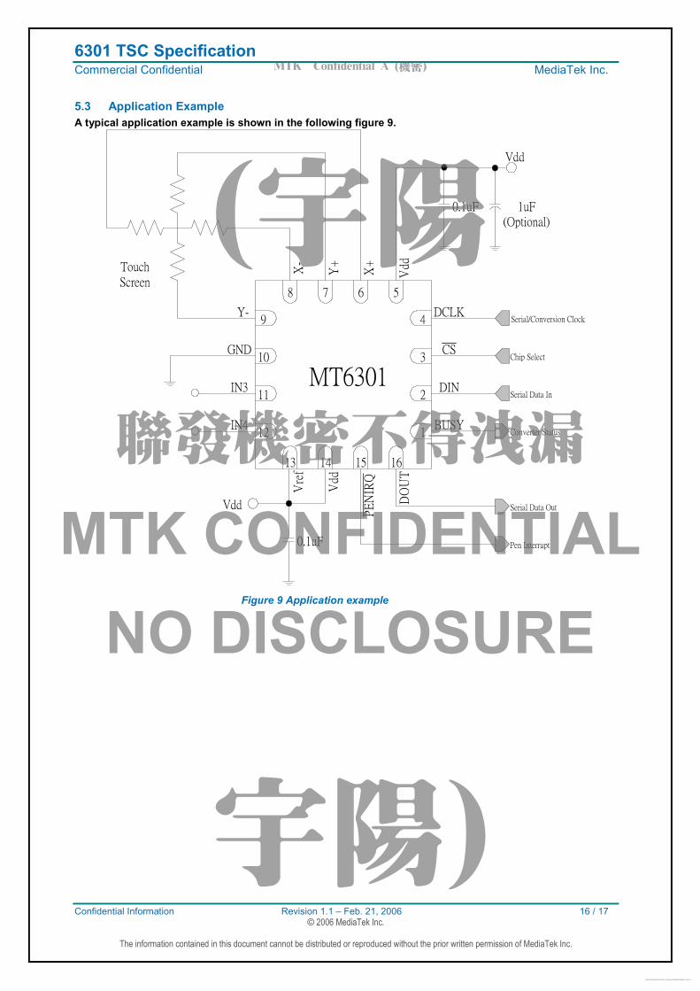
5.3 Application Example
A typical application example is shown in the following figure 9.
5678
9
10
11
12
13 14 15 16
1
2
3
4
MT6301Vdd
X+
Y+
X-
Y-
GND
IN3
IN4
Vref
Vdd
PENIR
Q
DOUT
BUSY
DIN
CS
DCLK
Touch
Screen
0.1uF 1uF
(Optional)
0.1uF
Vdd
Vdd
Serial/Conversion Clock
Chip Select
Serial Data In
Converter Status
Serial Data Out
Pen Interrupt
Figure 9 Application example
MTK Confidential A (機密)
(宇陽
聯發機密不得洩漏
MTK CONFIDENTIALNO DISCLOSURE
宇陽)Free Datasheet http://www.datasheetlist.com/
6301 TSC Specification Commercial Confidential MediaTek Inc.
Confidential Information Revision 1.1 – Feb. 21, 2006 17 / 17 © 2006 MediaTek Inc.
The information contained in this document cannot be distributed or reproduced without the prior written permission of MediaTek Inc.
6 Ordering Information
OODER NUMBER MARKING TEMP. RANGE PACKAGE
MT6301N MT6301N/AY -25°C to +85°C QFN 16-L, Pb-free
MT6301O MT6301O/AY -25°C to +85°C TSSOP 16-L, Pb-free
MTK Confidential A (機密)
(宇陽
聯發機密不得洩漏
MTK CONFIDENTIALNO DISCLOSURE
宇陽)Free Datasheet http://www.datasheetlist.com/
Recommended