2 ADC, 6 DAC,
96 kHz, 24-Bit Sigma-Delta Codec AD1839A
Rev. B Information furnished by Analog Devices is believed to be accurate and reliable. However, no responsibility is assumed by Analog Devices for its use, nor for any infringements of patents or other rights of third parties that may result from its use. Specifications subject to change without notice. No license is granted by implication or otherwise under any patent or patent rights of Analog Devices. Trademarks and registered trademarks are the property of their respective owners.
One Technology Way, P.O. Box 9106, Norwood, MA 02062-9106, U.S.A. Tel: 781.329.4700 www.analog.com Fax: 781.326.8703 © 2004 Analog Devices, Inc. All rights reserved.
FEATURES 5 V stereo audio system with 3.3 V tolerant digital interface Supports up to 96 kHz sample rates 192 kHz sample rate available on 1 DAC Supports 16-/20-/24-bit word lengths Multibit Σ-∆ modulators with perfect differential linearity
restoration for reduced idle tones and noise floor Data-directed scrambling DACs—least sensitive to jitter Single-ended output ADCs: −95 dB THD + N, 105 dB SNR and dynamic range DACs: −92 dB THD + N, 108 dB SNR and dynamic range On-chip volume controls per channel with 1024-step linear
scale DAC and ADC software controllable clickless mutes Digital de-emphasis processing Supports 256 × fS, 512 × fS, and 768 × fS master mode clocks Power-down mode and soft power-down mode Flexible serial data port with right-justified, left-justified,
I2S compatible, and DSP serial modes TDM interface mode supports 8-in/8-out operation using a
single SHARC® SPORT 52-lead MQFP plastic package
APPLICATIONS DVD video and audio players Home theater systems Automotive audio systems Audio/visual receivers Digital audio effects process
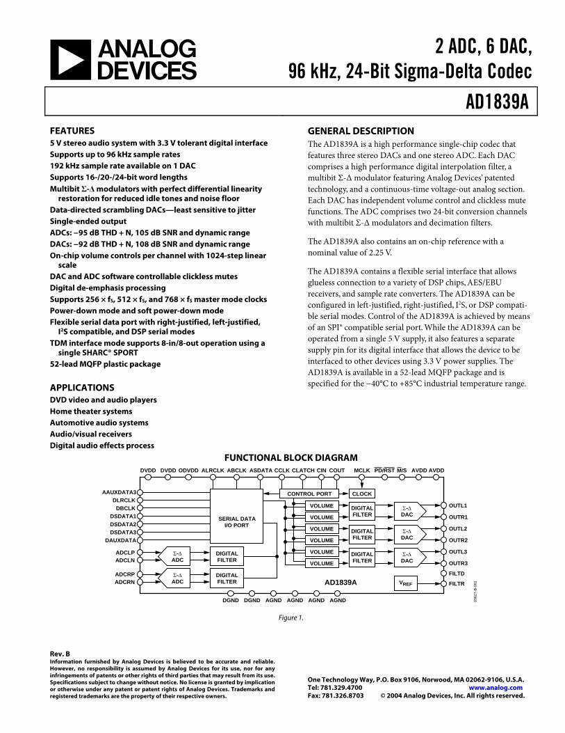
GENERAL DESCRIPTION The AD1839A is a high performance single-chip codec that features three stereo DACs and one stereo ADC. Each DAC comprises a high performance digital interpolation filter, a multibit Σ-∆ modulator featuring Analog Devices’ patented technology, and a continuous-time voltage-out analog section. Each DAC has independent volume control and clickless mute functions. The ADC comprises two 24-bit conversion channels with multibit Σ-∆ modulators and decimation filters.
The AD1839A also contains an on-chip reference with a nominal value of 2.25 V.
The AD1839A contains a flexible serial interface that allows glueless connection to a variety of DSP chips, AES/EBU receivers, and sample rate converters. The AD1839A can be configured in left-justified, right-justified, I2S, or DSP compati-ble serial modes. Control of the AD1839A is achieved by means of an SPI® compatible serial port. While the AD1839A can be operated from a single 5 V supply, it also features a separate supply pin for its digital interface that allows the device to be interfaced to other devices using 3.3 V power supplies. The AD1839A is available in a 52-lead MQFP package and is specified for the −40°C to +85°C industrial temperature range.
FUNCTIONAL BLOCK DIAGRAM
OUTL1
CONTROL PORT CLOCK
FILTD
FILTR
ADCLPADCLN
ADCRPADCRN
DLRCLKDBCLK
DSDATA1DSDATA2DSDATA3
DAUXDATA
MCLKODVDDDVDD AVDDAVDDDVDD
AGNDDGND
CINCLATCHCCLK COUT
DIGITALFILTER
DIGITALFILTER
M/S
VOLUME
SERIAL DATAI/O PORT
DIGITALFILTER
VREF
OUTR1VOLUME
OUTL2VOLUME DIGITALFILTER OUTR2VOLUME
OUTL3VOLUME DIGITALFILTER OUTR3VOLUME
Σ-∆ADC
AAUXDATA3
AD1839A
ASDATAABCLKALRCLK
AGND AGND AGNDDGND 0362
7-B-
001
Σ-∆ADC
Σ-∆DAC
Σ-∆DAC
Σ-∆DAC
PD/RST
Figure 1.
AD1839A
Rev. B | Page 2 of 24
TABLE OF CONTENTS Specifications..................................................................................... 3
Test Conditions............................................................................. 3
Timing Specifications....................................................................... 5
Absolute Maximum Ratings............................................................ 7
Temperature Range ...................................................................... 7
ESD Caution.................................................................................. 7
Pin Configuration and Function Descriptions............................. 8
Typical Performance Characteristics ............................................. 9
Terminology .................................................................................... 11
Functional Overview...................................................................... 12
ADCs............................................................................................ 12
DACs ............................................................................................ 12
DAC and ADC Coding.............................................................. 12
AD1839A Clocking Scheme ..................................................... 12
RESET and Power-Down .......................................................... 13
Power Supply and Voltage Reference....................................... 13
Serial Control Port ..................................................................... 13
Serial Data Ports—Data Format............................................... 14
Packed Modes ............................................................................. 14
Auxiliary Time Division Multiplexing (TDM) Mode ........... 14
Control/Status Registers ............................................................ 19
Cascade Mode............................................................................. 22
Outline Dimensions ....................................................................... 24
Ordering Guide .......................................................................... 24
REVISION HISTORY
5/04—Data Sheet Changed from Rev. A to Rev. B Updated Format Universal Changes to Data Sheet Title1
2/04—Data Sheet Changed from Rev. 0 to Rev. A Changes to Ordering Guide ............................................................. 6 Deleted Clock Signals Section ....................................................... 11 Added AD1835A Clocking Scheme Section................................ 11 Added Table II and Table III and renumbered following tables 11 Changes to Auxiliary (TDM Mode) Section................................ 13 Changes to Figure 5......................................................................... 14 Changes to Figure 6......................................................................... 14 Added Figures 7a and 8a................................................................. 15 Renamed Figure 7 and Figure 8 to Figure 7b and Figure 8b ..... 15 Changes to Figure 9......................................................................... 15 Changes to Table VIII ..................................................................... 21 Updated Outline Dimensions ........................................................ 24
AD1839A
Rev. B | Page 3 of 24
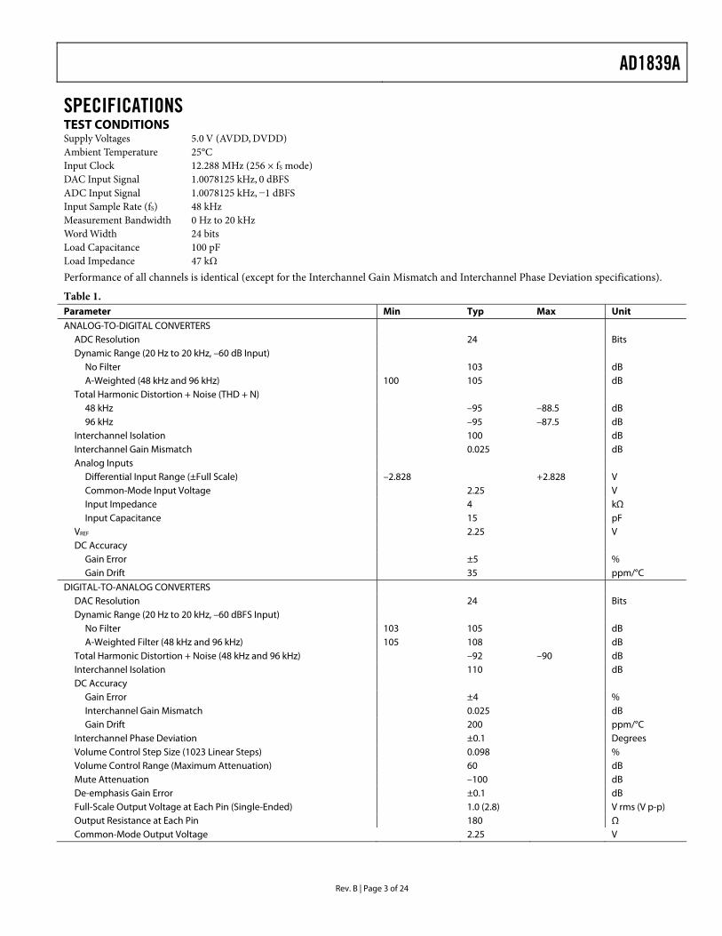
SPECIFICATIONS TEST CONDITIONS Supply Voltages 5.0 V (AVDD, DVDD) Ambient Temperature 25°C Input Clock 12.288 MHz (256 × fS mode) DAC Input Signal 1.0078125 kHz, 0 dBFS ADC Input Signal 1.0078125 kHz, −1 dBFS Input Sample Rate (fS) 48 kHz Measurement Bandwidth 0 Hz to 20 kHz Word Width 24 bits Load Capacitance 100 pF Load Impedance 47 kΩ Performance of all channels is identical (except for the Interchannel Gain Mismatch and Interchannel Phase Deviation specifications).
Table 1. Parameter Min Typ Max Unit ANALOG-TO-DIGITAL CONVERTERS
ADC Resolution 24 Bits Dynamic Range (20 Hz to 20 kHz, –60 dB Input)
No Filter 103 dB A-Weighted (48 kHz and 96 kHz) 100 105 dB
Total Harmonic Distortion + Noise (THD + N) 48 kHz –95 –88.5 dB 96 kHz –95 –87.5 dB
Interchannel Isolation 100 dB Interchannel Gain Mismatch 0.025 dB Analog Inputs
Differential Input Range (±Full Scale) –2.828 +2.828 V Common-Mode Input Voltage 2.25 V Input Impedance 4 kΩ Input Capacitance 15 pF
VREF 2.25 V DC Accuracy
Gain Error ±5 % Gain Drift 35 ppm/°C
DIGITAL-TO-ANALOG CONVERTERS DAC Resolution 24 Bits Dynamic Range (20 Hz to 20 kHz, –60 dBFS Input)
No Filter 103 105 dB A-Weighted Filter (48 kHz and 96 kHz) 105 108 dB
Total Harmonic Distortion + Noise (48 kHz and 96 kHz) –92 –90 dB Interchannel Isolation 110 dB DC Accuracy
Gain Error ±4 % Interchannel Gain Mismatch 0.025 dB Gain Drift 200 ppm/°C
Interchannel Phase Deviation ±0.1 Degrees Volume Control Step Size (1023 Linear Steps) 0.098 % Volume Control Range (Maximum Attenuation) 60 dB Mute Attenuation –100 dB De-emphasis Gain Error ±0.1 dB Full-Scale Output Voltage at Each Pin (Single-Ended) 1.0 (2.8) V rms (V p-p) Output Resistance at Each Pin 180 Ω Common-Mode Output Voltage 2.25 V

AD1839A
Rev. B | Page 4 of 24
Parameter Min Typ Max Unit ADC DECIMATION FILTER, 48 kHz1
Pass Band 21.77 kHz Pass-Band Ripple ±0.01 dB Stop Band 26.23 kHz Stop-Band Attenuation 120 dB Group Delay 910 µs
ADC DECIMATION FILTER, 96 kHz1 Pass Band 43.54 kHz Pass-Band Ripple ±0.01 dB Stop Band 52.46 kHz Stop-Band Attenuation 120 dB Group Delay 460 µs
DAC INTERPOLATION FILTER, 48 kHz1 Pass Band 21.77 kHz Pass-Band Ripple ±0.01 dB Stop Band 28 kHz Stop-Band Attenuation 55 dB Group Delay 340 µs
DAC INTERPOLATION FILTER, 96 kHz1 Pass Band 43.54 kHz Pass-Band Ripple ±0.01 dB Stop Band 52 kHz Stop-Band Attenuation 55 dB Group Delay 160 µs
DAC INTERPOLATION FILTER, 192 kHz1 Pass Band 81.2 kHz Pass-Band Ripple ±0.06 dB Stop Band 97 kHz Stop-Band Attenuation 80 dB Group Delay 110 µs
DIGITAL I/O Input Voltage High 2.4 V Input Voltage Low 0.8 V Output Voltage High ODVDD – 0.4 V Output Voltage Low 0.4 V Leakage Current ±10 µA
POWER SUPPLIES Supply Voltage (AVDD and DVDD) 4.5 5.0 5.5 V Supply Voltage (ODVDD) 3.0 DVDD V Supply Current IANALOG 84 95 mA Supply Current IANALOG, Power-Down 55 67 mA Supply Current IDIGITAL 64 74 mA Supply Current IDIGITAL, Power-Down 1 4.5 mA Dissipation
Operation, Both Supplies 740 mW Operation, Analog Supply 420 mW Operation, Digital Supply 320 mW
Power-Down, Both Supplies 280 mW Power Supply Rejection Ratio
1 kHz, 300 mV p-p Signal at Analog Supply Pins –70 dB 20 kHz, 300 mV p-p Signal at Analog Supply Pins –75 dB
1 Guaranteed by design.
AD1839A
Rev. B | Page 5 of 24
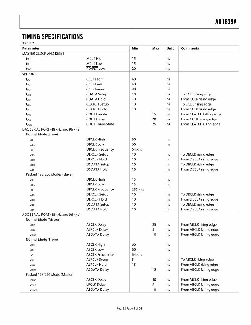
TIMING SPECIFICATIONS Table 2. Parameter Min Max Unit Comments MASTER CLOCK AND RESET
tMH MCLK High 15 ns tML MCLK Low 15 ns tPDR PD/RST Low 20 ns
SPI PORT tCCH CCLK High 40 ns tCCL CCLK Low 40 ns tCCP CCLK Period 80 ns tCDS CDATA Setup 10 ns To CCLK rising edge tCDH CDATA Hold 10 ns From CCLK rising edge tCLS CLATCH Setup 10 ns To CCLK rising edge tCLH CLATCH Hold 10 ns From CCLK rising edge tCOE COUT Enable 15 ns From CLATCH falling edge tCOD COUT Delay 20 ns From CCLK falling edge tCOTS COUT Three-State 25 ns From CLATCH rising edge
DAC SERIAL PORT (48 kHz and 96 kHz) Normal Mode (Slave)
tDBH DBCLK High 60 ns tDBL DBCLK Low 60 ns fDB DBCLK Frequency 64 × fS tDLS DLRCLK Setup 10 ns To DBCLK rising edge tDLH DLRCLK Hold 10 ns From DBCLK rising edge tDDS DSDATA Setup 10 ns To DBCLK rising edge tDDH DSDATA Hold 10 ns From DBCLK rising edge
Packed 128/256 Modes (Slave) tDBH DBCLK High 15 ns tDBL DBCLK Low 15 ns fDB DBCLK Frequency 256 × fS tDLS DLRCLK Setup 10 ns To DBCLK rising edge tDLH DLRCLK Hold 10 ns From DBCLK rising edge tDDS DSDATA Setup 10 ns To DBCLK rising edge tDDH DSDATA Hold 10 ns From DBCLK rising edge
ADC SERIAL PORT (48 kHz and 96 kHz) Normal Mode (Master)
tABD ABCLK Delay 25 ns From MCLK rising edge tALD ALRCLK Delay 5 ns From ABCLK falling edge tABDD ASDATA Delay 10 ns From ABCLK falling edge
Normal Mode (Slave) tABH ABCLK High 60 ns tABL ABCLK Low 60 ns fAB ABCLK Frequency 64 × fS tALS ALRCLK Setup 5 ns To ABCLK rising edge tALH ALRCLK Hold 15 ns From ABCLK rising edge tABDD ASDATA Delay 15 ns From ABCLK falling edge
Packed 128/256 Mode (Master) tPABD ABCLK Delay 40 ns From MCLK rising edge tPALD LRCLK Delay 5 ns From ABCLK falling edge tPABDD ASDATA Delay 10 ns From ABCLK falling edge
AD1839A
Rev. B | Page 6 of 24
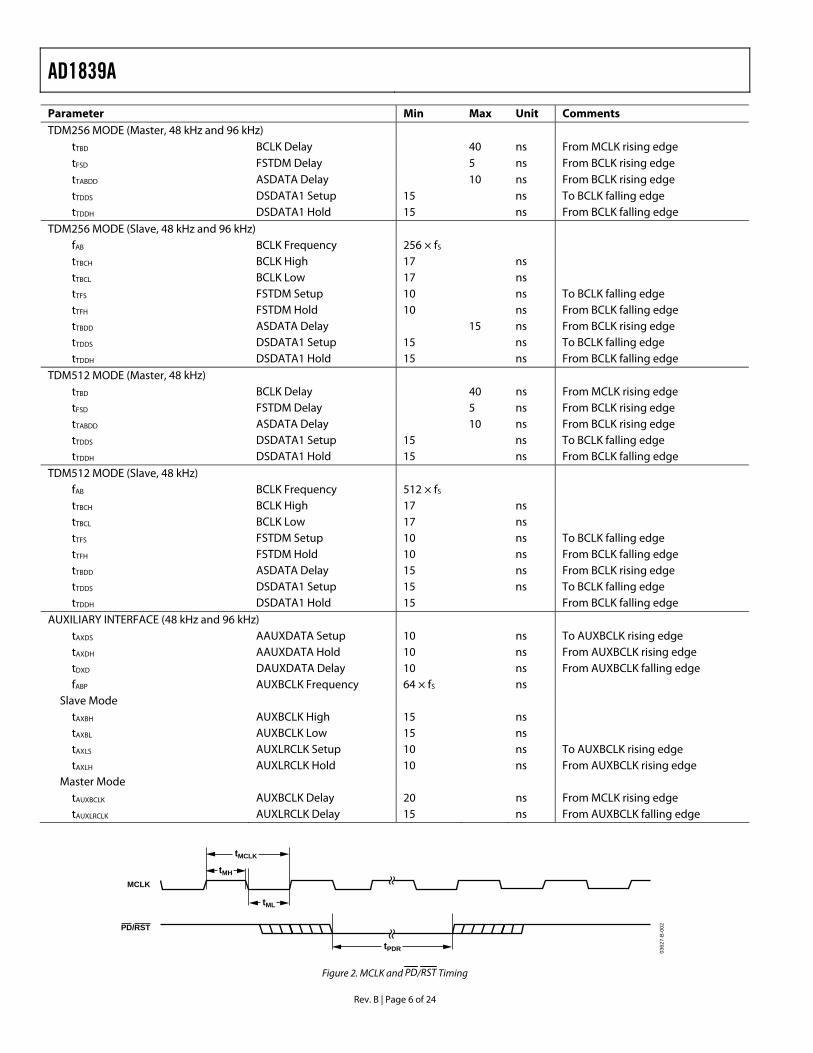
Parameter Min Max Unit Comments TDM256 MODE (Master, 48 kHz and 96 kHz)
tTBD BCLK Delay 40 ns From MCLK rising edge tFSD FSTDM Delay 5 ns From BCLK rising edge tTABDD ASDATA Delay 10 ns From BCLK rising edge tTDDS DSDATA1 Setup 15 ns To BCLK falling edge tTDDH DSDATA1 Hold 15 ns From BCLK falling edge
TDM256 MODE (Slave, 48 kHz and 96 kHz) fAB BCLK Frequency 256 × fS tTBCH BCLK High 17 ns tTBCL BCLK Low 17 ns tTFS FSTDM Setup 10 ns To BCLK falling edge tTFH FSTDM Hold 10 ns From BCLK falling edge tTBDD ASDATA Delay 15 ns From BCLK rising edge tTDDS DSDATA1 Setup 15 ns To BCLK falling edge tTDDH DSDATA1 Hold 15 ns From BCLK falling edge
TDM512 MODE (Master, 48 kHz) tTBD BCLK Delay 40 ns From MCLK rising edge tFSD FSTDM Delay 5 ns From BCLK rising edge tTABDD ASDATA Delay 10 ns From BCLK rising edge tTDDS DSDATA1 Setup 15 ns To BCLK falling edge tTDDH DSDATA1 Hold 15 ns From BCLK falling edge
TDM512 MODE (Slave, 48 kHz) fAB BCLK Frequency 512 × fS tTBCH BCLK High 17 ns tTBCL BCLK Low 17 ns tTFS FSTDM Setup 10 ns To BCLK falling edge tTFH FSTDM Hold 10 ns From BCLK falling edge tTBDD ASDATA Delay 15 ns From BCLK rising edge tTDDS DSDATA1 Setup 15 ns To BCLK falling edge tTDDH DSDATA1 Hold 15 From BCLK falling edge
AUXILIARY INTERFACE (48 kHz and 96 kHz) tAXDS AAUXDATA Setup 10 ns To AUXBCLK rising edge tAXDH AAUXDATA Hold 10 ns From AUXBCLK rising edge tDXD DAUXDATA Delay 10 ns From AUXBCLK falling edge fABP AUXBCLK Frequency 64 × fS ns
Slave Mode tAXBH AUXBCLK High 15 ns tAXBL AUXBCLK Low 15 ns tAXLS AUXLRCLK Setup 10 ns To AUXBCLK rising edge tAXLH AUXLRCLK Hold 10 ns From AUXBCLK rising edge
Master Mode tAUXBCLK AUXBCLK Delay 20 ns From MCLK rising edge tAUXLRCLK AUXLRCLK Delay 15 ns From AUXBCLK falling edge
MCLK
0362
7-B-
002
tPDR
tML
tMH
tMCLK
PD/RST
Figure 2. MCLK and PD/RST Timing
AD1839A
Rev. B | Page 7 of 24
ABSOLUTE MAXIMUM RATINGS TA = 25°C, unless otherwise noted.
Table 3. Parameter Rating AVDD, DVDD, ODVDD to AGND, DGND −0.3 V to +6.0 V AGND to DGND −0.3 V to +0.3 V Digital I/O Voltage to DGND −0.3 V to ODVDD + 0.3 V Analog I/O Voltage to AGND −0.3 V to AVDD + 0.3 V Operating Temperature Range Industrial (A Version) −40°C to +85°C
TEMPERATURE RANGE Table 4. Parameter Min Typ Max Unit Specifications Guaranteed +25 °C Functionality Guaranteed −40 +85 °C Storage −65 +150 °C
Stresses above those listed under Absolute Maximum Ratings may cause permanent damage to the device. This is a stress rating only; functional operation of the device at these or any other conditions above those listed in the operational sections of this specification is not implied. Exposure to absolute maximum rating conditions for extended periods may affect device reliability.
ESD CAUTION ESD (electrostatic discharge) sensitive device. Electrostatic charges as high as 4000 V readily accumulate on the human body and test equipment and can discharge without detection. Although this product features proprietary ESD protection circuitry, permanent damage may occur on devices subjected to high energy electrostatic discharges. Therefore, proper ESD precautions are recommended to avoid performance degradation or loss of functionality.
AD1839A
Rev. B | Page 8 of 24
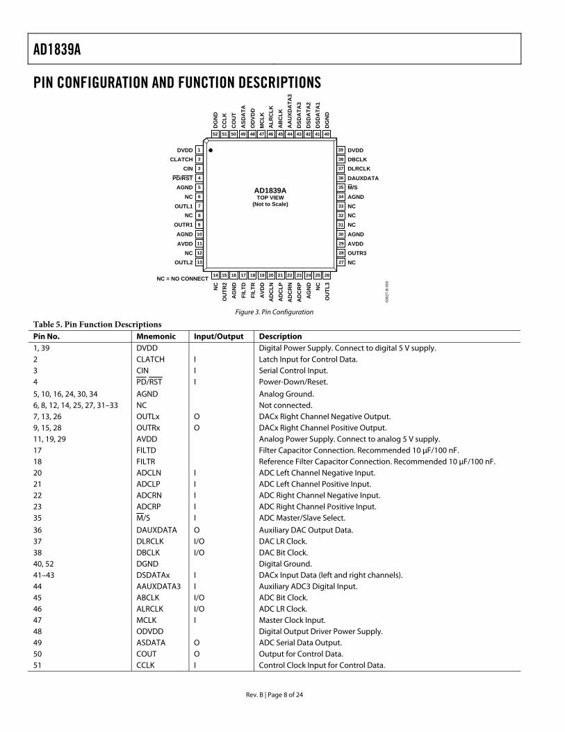
PIN CONFIGURATION AND FUNCTION DESCRIPTIONS
0362
7-B-
003
52
DG
ND
51
CC
LK
50
CO
UT
49
ASD
ATA
48
OD
VDD
47
MC
LK
46
ALR
CLK
45
AB
CLK
44
AA
UXD
ATA
3
43
DSD
ATA
3
42
DSD
ATA
2
41
DSD
ATA
1
40
DG
ND
38 DBCLK37 DLRCLK36 DAUXDATA
33 NC
34 AGND
35 M/S
39 DVDD
32 NC31 NC30 AGND
28 OUTR327 NC
29 AVDD
2CLATCH3CIN4PD/RST
7OUTL1
6NC
5AGND
1DVDD
8NC9OUTR110AGND
12NC13OUTL2
11AVDD
NC = NO CONNECT 14
NC
15
OU
TR2
16
AG
ND
17
FILT
D
18
FILT
R
19
AVD
D
20A
DC
LN21
AD
CLP
22
AD
CR
N
23
AD
CR
P
24
AG
ND
25
NC
26
OU
TL3
AD1839ATOP VIEW
(Not to Scale)
Figure 3. Pin Configuration
Table 5. Pin Function Descriptions Pin No. Mnemonic Input/Output Description 1, 39 DVDD Digital Power Supply. Connect to digital 5 V supply. 2 CLATCH I Latch Input for Control Data. 3 CIN I Serial Control Input. 4 PD/RST I Power-Down/Reset.
5, 10, 16, 24, 30, 34 AGND Analog Ground. 6, 8, 12, 14, 25, 27, 31–33 NC Not connected. 7, 13, 26 OUTLx O DACx Right Channel Negative Output. 9, 15, 28 OUTRx O DACx Right Channel Positive Output. 11, 19, 29 AVDD Analog Power Supply. Connect to analog 5 V supply. 17 FILTD Filter Capacitor Connection. Recommended 10 µF/100 nF. 18 FILTR Reference Filter Capacitor Connection. Recommended 10 µF/100 nF. 20 ADCLN I ADC Left Channel Negative Input. 21 ADCLP I ADC Left Channel Positive Input. 22 ADCRN I ADC Right Channel Negative Input. 23 ADCRP I ADC Right Channel Positive Input. 35 M/S I ADC Master/Slave Select.
36 DAUXDATA O Auxiliary DAC Output Data. 37 DLRCLK I/O DAC LR Clock. 38 DBCLK I/O DAC Bit Clock. 40, 52 DGND Digital Ground. 41–43 DSDATAx I DACx Input Data (left and right channels). 44 AAUXDATA3 I Auxiliary ADC3 Digital Input. 45 ABCLK I/O ADC Bit Clock. 46 ALRCLK I/O ADC LR Clock. 47 MCLK I Master Clock Input. 48 ODVDD Digital Output Driver Power Supply. 49 ASDATA O ADC Serial Data Output. 50 COUT O Output for Control Data. 51 CCLK I Control Clock Input for Control Data.

AD1839A
Rev. B | Page 9 of 24
TYPICAL PERFORMANCE CHARACTERISTICS
0362
7-B-
004
FREQUENCY (Normalized to fS)0 5 10 15
MA
GN
ITU
DE
(dB
)
0
–50
–100
–150
Figure 4. ADC Composite Filter Response
0362
7-B-
005
FREQUENCY (Hz)0 205 10 15
MA
GN
ITU
DE
(dB
)
–30
–25
–20
–15
–10
–5
0
5
Figure 5. ADC High-Pass Filter Response, fS = 48 kHz
0362
7-B-
006
FREQUENCY (Normalized to fS)0 2.00.5 1.0 1.5
MA
GN
ITU
DE
(dB
)
–150
0
–100
–50
Figure 6. ADC Composite Filter Response (Pass-Band Section)
0362
7-B-
007
FREQUENCY (Hz)0 25 10 15
MA
GN
ITU
DE
(dB
)
–30
–25
–20
–15
–10
–5
0
5
0
Figure 7. ADC High-Pass Filter Response, fS = 96 kHz
0362
7-B-
008
FREQUENCY (kHz)2000 50 100 150
MA
GN
ITU
DE
(dB
)
–150
0
–50
–100
Figure 8. DAC Composite Filter Response, fS = 48 kHz
0362
7-B-
009
FREQUENCY (kHz)2000
MA
GN
ITU
DE
(dB
)
0
–50
–150
–100
50 100 150
Figure 9. DAC Composite Filter Response, fS = 96 kHz
AD1839A
Rev. B | Page 10 of 24
0362
7-B-
010
FREQUENCY (kHz)2000 50 100 150
MA
GN
ITU
DE
(dB
)
0
–50
–100
–150
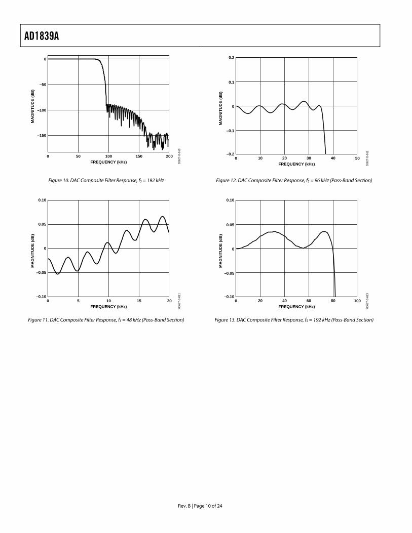
Figure 10. DAC Composite Filter Response, fS = 192 kHz
0362
7-B-
011
FREQUENCY (kHz)200
MA
GN
ITU
DE
(dB
)
0.10
0.05
–0.10
0
–0.05
5 10 15
Figure 11. DAC Composite Filter Response, fS = 48 kHz (Pass-Band Section)
0362
7-B-
012
FREQUENCY (kHz)500 10 20 30 40
MA
GN
ITU
DE
(dB
)
0.2
0.1
–0.2
0
–0.1
Figure 12. DAC Composite Filter Response, fS = 96 kHz (Pass-Band Section)
0362
7-B-
013
FREQUENCY (kHz)1000
MA
GN
ITU
DE
(dB
)
0.10
0.05
–0.10
0
–0.05
20 40 60 80
Figure 13. DAC Composite Filter Response, fS = 192 kHz (Pass-Band Section)

AD1839A
Rev. B | Page 11 of 24
TERMINOLOGY Dynamic Range
The ratio of a full-scale input signal to the integrated input noise in the pass band (20 Hz to 20 kHz), expressed in decibels. Dynamic range is measured with a −60 dB input signal and is equal to (S/[THD + N]) + 60 dB. Note that spurious harmonics are below the noise with a −60 dB input, so the noise level establishes the dynamic range. The dynamic range is specified with and without an A-weight filter applied.
Signal-to-(Total Harmonic Distortion + Noise) [S/(THD + N)]
The ratio of the root-mean-square (rms) value of the fundamental input signal to the rms sum of all other spectral components in the pass band, expressed in decibels.
Pass Band
The region of the frequency spectrum unaffected by the attenuation of the digital decimator’s filter.
Pass-Band Ripple
The peak-to-peak variation in amplitude response from equal-amplitude input signal frequencies within the pass band, expressed in decibels.
Stop Band
The region of the frequency spectrum attenuated by the digital decimator’s filter to the degree specified by stop-band attenuation.
Gain Error
With identical near full-scale inputs, the ratio of actual output to expected output, expressed as a percentage.
Interchannel Gain Mismatch
With identical near full-scale inputs, the ratio of outputs of the two stereo channels, expressed in decibels.
Gain Drift
Change in response to a near full-scale input with a change in temperature, expressed as parts-per-million (ppm) per °C.
Crosstalk (EIAJ Method)
Ratio of response on one channel with a grounded input to a full-scale 1 kHz sine wave input on the other channel, expressed in decibels.
Power Supply Rejection
With no analog input, signal present at the output when a 300 mV p-p signal is applied to the power supply pins, expressed in decibels of full scale.
Group Delay
Intuitively, the time interval required for an input pulse to appear at the converter’s output, expressed in microseconds. More precisely, the derivative of radian phase with respect to the radian frequency at a given frequency.
Group Delay Variation
The difference in group delays at different input frequencies. Specified as the difference between the largest and the smallest group delays in the pass band, expressed in microseconds.
Acronyms
ADC—Analog-to-digital converter.
DAC—Digital-to-analog converter.
DSP—Digital signal processor.
IMCLK—Internal master clock signal used to clock the ADC and DAC engines.
MCLK—External master clock signal applied to the AD1839A.

AD1839A
Rev. B | Page 12 of 24
FUNCTIONAL OVERVIEWADCS There are two ADC channels in the AD1839A, configured as a stereo pair. Each ADC has fully differential inputs. The ADC section can operate at a sample rate of up to 96 kHz. The ADCs include on-board digital decimation filters with 120 dB stop-band attenuation and linear phase response, operating at an oversampling ratio of 128 (for 48 kHz operation) or 64 (for 96 kHz operation).
The peak level information for each ADC may be read from the ADC Peak 0 and ADC Peak 1 registers. The data is supplied as a 6-bit word with a maximum range of 0 dB to −63 dB and a resolution of 1 dB. The registers hold peak information until read; after reading, the registers are reset so that new peak information can be acquired. (Refer to the register description in Table 10 for details of the format.) The two ADC channels have a common serial bit clock and a left-right framing clock. The clock signals are all synchronous with the sample rate.
The ADC digital pins, ABCLK and ALRCLK, can be set to operate as inputs or outputs by connecting the M/S pin to ODVDD or DGND, respectively. When the pins are set as outputs, the AD1839A generates the timing signals. When the pins are set as inputs, the timing must be generated by the external audio controller.
DACS The AD1839A has six DAC channels arranged as three independent stereo pairs, with six single-ended analog outputs. Each channel has its own independently programmable attenuator, adjustable in 1,024 linear steps. Digital inputs are supplied through three serial data input pins (one for each stereo pair) and a common frame (DLRCLK) and bit clock (DBCLK). Alternatively, one of the packed data modes can be used to access all six channels on a single TDM data pin. A stereo replicate feature is included where the DAC data sent to the first DAC pair is also sent to the other DACs in the part. The AD1839A can accept DAC data at a sample rate of 192 kHz on DAC 1 only. The stereo replicate feature can then be used to copy the audio data to the other DACs.
Each of the output pins sits at a dc level of VREF and swings ±1.4 V for a 0 dB digital input signal. A single op amp, third-order, external low-pass filter is recommended to remove high frequency noise present on the output pins. Note that the use of op amps with low slew rate or low bandwidth may cause high frequency noise and tones to fold down into the audio band; care should be exercised in selecting these components.
The FILTD pin should be connected to an external grounded capacitor. This pin reduces the noise of the internal DAC bias circuitry, thus reducing the DAC output noise. At times, this capacitor may be eliminated with little effect on performance.
DAC AND ADC CODING The DAC and ADC output data stream is in a twos complement encoded format. A 16-bit, 20-bit, or 24-bit word width can be selected. The coding scheme is detailed in Table 6.
Table 6. Coding Scheme Code Level 01111......1111 +FS 00000......0000 0 (Ref level) 10000......0000 −FS
AD1839A CLOCKING SCHEME By default, the AD1839A requires an MCLK signal that is 256 times the required sample frequency up to a maximum of 12.288 MHz. The AD1839A uses a clock scaler to double the clock frequency for use internally. The default setting of the clock scaler is Multiply by 2. The clock scaler can also be set to Multiply by 1 (bypass) or Multiply by 2/3. The clock scaler is controlled by programming the bits in the ADC Control 3 register. The internal MCLK signal, IMCLK, should not exceed 24.576 MHz to ensure correct operation.
The MCLK of the AD1839A should remain constant during normal operation of the DAC and ADC. If it is required to change the MCLK rate, the AD1838A should be reset. Also, if MCLK scaler needs to be modified so that the IMCLK does not exceed 24.576 MHz, this should be done during the internal reset phase of the AD1839A by programming the bits in the first 3,072 MCLK periods following the reset.
Selecting the DAC Sampling Rate
The AD1839A DAC engine has a programmable interpolator that allows the user to select different interpolation rates based on the required sample rate and MCLK value available. Table 7 shows the settings required for sample rates based on a fixed MCLK of 12.288 MHz.
Table 7. DAC Sample Rate Settings Sample Rate Interpolator Rate DAC Control 1 Register 48 kHz 8× 000000xxxxxxxx00 96 kHz 4× 000000xxxxxxxx01 192 kHz 2× 000000xxxxxxxx10
Selecting an ADC Sample Rate
The AD1839A ADC engine has a programmable decimator that allows the user to select the sample rate based on the MCLK value. By default, the output sample rate is IMCLK/512. To achieve a sample rate of IMCLK/256, the sample rate bit in the ADC Control 1 register should be set as shown in Table 8.
Table 8. ADC Sample Rate Settings Sample Rate ADC Control 1 Register IMCLK/512 1100000xx0xxxxxx (48 kHz) IMCLK/256 1100000xx1xxxxxx (96 kHz)
AD1839A
Rev. B | Page 13 of 24
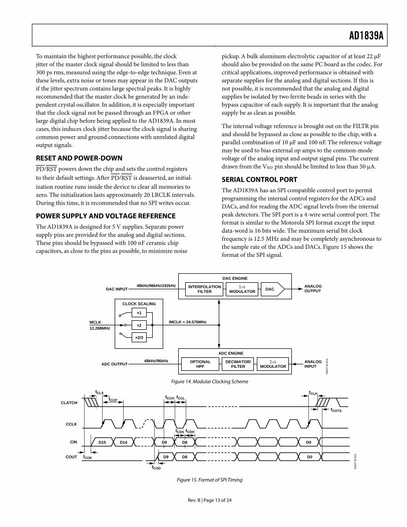
To maintain the highest performance possible, the clock jitter of the master clock signal should be limited to less than 300 ps rms, measured using the edge-to-edge technique. Even at these levels, extra noise or tones may appear in the DAC outputs if the jitter spectrum contains large spectral peaks. It is highly recommended that the master clock be generated by an inde-pendent crystal oscillator. In addition, it is especially important that the clock signal not be passed through an FPGA or other large digital chip before being applied to the AD1839A. In most cases, this induces clock jitter because the clock signal is sharing common power and ground connections with unrelated digital output signals.
RESET AND POWER-DOWN
PD/RST powers down the chip and sets the control registers to their default settings. After PD/RST is deasserted, an initial-ization routine runs inside the device to clear all memories to zero. The initialization lasts approximately 20 LRCLK intervals. During this time, it is recommended that no SPI writes occur.
POWER SUPPLY AND VOLTAGE REFERENCE The AD1839A is designed for 5 V supplies. Separate power supply pins are provided for the analog and digital sections. These pins should be bypassed with 100 nF ceramic chip capacitors, as close to the pins as possible, to minimize noise
pickup. A bulk aluminum electrolytic capacitor of at least 22 µF should also be provided on the same PC board as the codec. For critical applications, improved performance is obtained with separate supplies for the analog and digital sections. If this is not possible, it is recommended that the analog and digital supplies be isolated by two ferrite beads in series with the bypass capacitor of each supply. It is important that the analog supply be as clean as possible.
The internal voltage reference is brought out on the FILTR pin and should be bypassed as close as possible to the chip, with a parallel combination of 10 µF and 100 nF. The reference voltage may be used to bias external op amps to the common-mode voltage of the analog input and output signal pins. The current drawn from the VREF pin should be limited to less than 50 µA.
SERIAL CONTROL PORT The AD1839A has an SPI compatible control port to permit programming the internal control registers for the ADCs and DACs, and for reading the ADC signal levels from the internal peak detectors. The SPI port is a 4-wire serial control port. The format is similar to the Motorola SPI format except the input data-word is 16 bits wide. The maximum serial bit clock frequency is 12.5 MHz and may be completely asynchronous to the sample rate of the ADCs and DACs. Figure 15 shows the format of the SPI signal.
CLOCK SCALING
×1
×2
×2/3
MCLK12.288MHz
DAC INPUT
ADC OUTPUT
DAC ENGINE
INTERPOLATIONFILTER
Σ-∆MODULATOR DAC
48kHz/96kHz/192kHz
48kHz/96kHz
ANALOGOUTPUT
ANALOGINPUT
IMCLK = 24.576MHz03
627-
B-01
4
ADC ENGINE
OPTIONALHPF
DECIMATOR/FILTER
Σ-∆MODULATOR
Figure 14. Modular Clocking Scheme
CLATCH
CCLK
CIN
COUT
D0
D8 D0
D15 D14
D9
D8
tCCH tCCL
D9
tCDS tCDH
tCLS tCLH
tCOD
tCOTS
tCCP
tCOE
0362
7-B-
015
Figure 15. Format of SPI Timing
AD1839A
Rev. B | Page 14 of 24
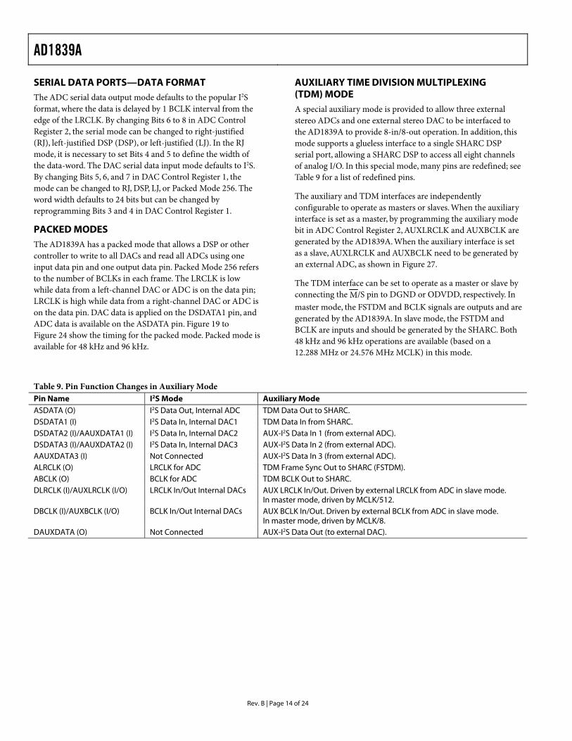
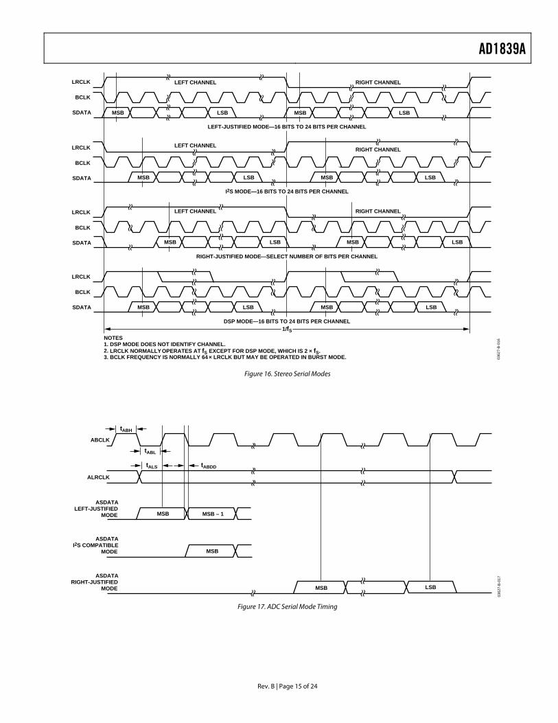
SERIAL DATA PORTS—DATA FORMAT The ADC serial data output mode defaults to the popular I2S format, where the data is delayed by 1 BCLK interval from the edge of the LRCLK. By changing Bits 6 to 8 in ADC Control Register 2, the serial mode can be changed to right-justified (RJ), left-justified DSP (DSP), or left-justified (LJ). In the RJ mode, it is necessary to set Bits 4 and 5 to define the width of the data-word. The DAC serial data input mode defaults to I2S. By changing Bits 5, 6, and 7 in DAC Control Register 1, the mode can be changed to RJ, DSP, LJ, or Packed Mode 256. The word width defaults to 24 bits but can be changed by reprogramming Bits 3 and 4 in DAC Control Register 1.
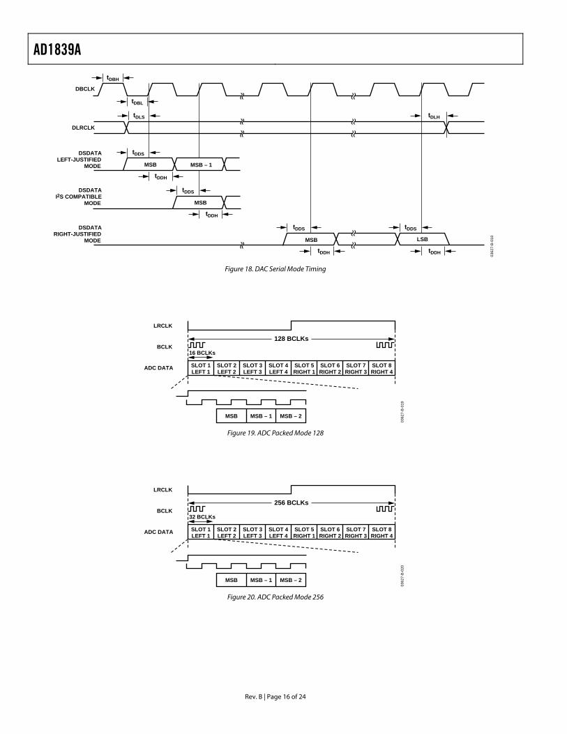
PACKED MODES The AD1839A has a packed mode that allows a DSP or other controller to write to all DACs and read all ADCs using one input data pin and one output data pin. Packed Mode 256 refers to the number of BCLKs in each frame. The LRCLK is low while data from a left-channel DAC or ADC is on the data pin; LRCLK is high while data from a right-channel DAC or ADC is on the data pin. DAC data is applied on the DSDATA1 pin, and ADC data is available on the ASDATA pin. Figure 19 to Figure 24 show the timing for the packed mode. Packed mode is available for 48 kHz and 96 kHz.
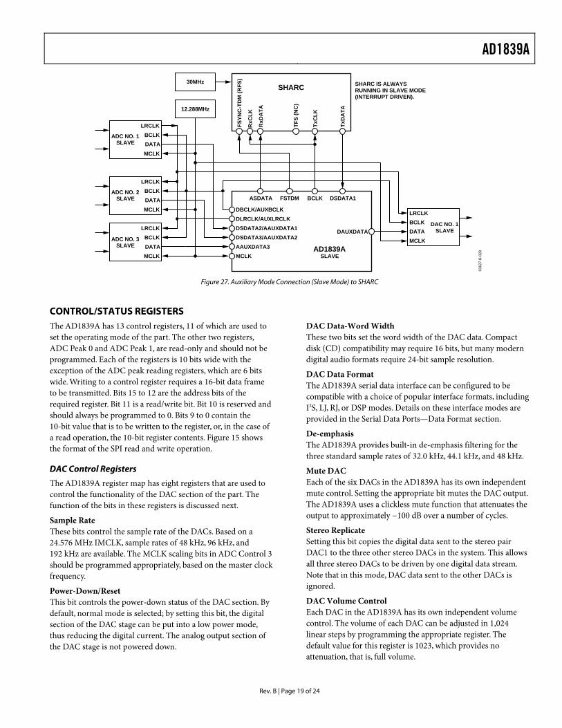
AUXILIARY TIME DIVISION MULTIPLEXING (TDM) MODE A special auxiliary mode is provided to allow three external stereo ADCs and one external stereo DAC to be interfaced to the AD1839A to provide 8-in/8-out operation. In addition, this mode supports a glueless interface to a single SHARC DSP serial port, allowing a SHARC DSP to access all eight channels of analog I/O. In this special mode, many pins are redefined; see Table 9 for a list of redefined pins.
The auxiliary and TDM interfaces are independently configurable to operate as masters or slaves. When the auxiliary interface is set as a master, by programming the auxiliary mode bit in ADC Control Register 2, AUXLRCLK and AUXBCLK are generated by the AD1839A. When the auxiliary interface is set as a slave, AUXLRCLK and AUXBCLK need to be generated by an external ADC, as shown in Figure 27.
The TDM interface can be set to operate as a master or slave by connecting the M/S pin to DGND or ODVDD, respectively. In master mode, the FSTDM and BCLK signals are outputs and are generated by the AD1839A. In slave mode, the FSTDM and BCLK are inputs and should be generated by the SHARC. Both 48 kHz and 96 kHz operations are available (based on a 12.288 MHz or 24.576 MHz MCLK) in this mode.
Table 9. Pin Function Changes in Auxiliary Mode Pin Name I2S Mode Auxiliary Mode ASDATA (O) I2S Data Out, Internal ADC TDM Data Out to SHARC. DSDATA1 (I) I2S Data In, Internal DAC1 TDM Data In from SHARC. DSDATA2 (I)/AAUXDATA1 (I) I2S Data In, Internal DAC2 AUX-I2S Data In 1 (from external ADC). DSDATA3 (I)/AAUXDATA2 (I) I2S Data In, Internal DAC3 AUX-I2S Data In 2 (from external ADC). AAUXDATA3 (I) Not Connected AUX-I2S Data In 3 (from external ADC). ALRCLK (O) LRCLK for ADC TDM Frame Sync Out to SHARC (FSTDM). ABCLK (O) BCLK for ADC TDM BCLK Out to SHARC. DLRCLK (I)/AUXLRCLK (I/O) LRCLK In/Out Internal DACs AUX LRCLK In/Out. Driven by external LRCLK from ADC in slave mode.
In master mode, driven by MCLK/512. DBCLK (I)/AUXBCLK (I/O) BCLK In/Out Internal DACs AUX BCLK In/Out. Driven by external BCLK from ADC in slave mode.
In master mode, driven by MCLK/8. DAUXDATA (O) Not Connected AUX-I2S Data Out (to external DAC).
AD1839A
Rev. B | Page 15 of 24
LRCLK
BCLK
SDATA
LRCLK
BCLK
SDATA
LRCLK
BCLK
SDATA
LRCLK
BCLK
SDATA
LEFT CHANNEL RIGHT CHANNEL
LEFT CHANNELRIGHT CHANNEL
LEFT CHANNEL RIGHT CHANNEL
MSB MSB
MSB MSB
MSB MSB
MSB MSB
LSB LSB
LSB LSB
LSB LSB
LSB LSB
LEFT-JUSTIFIED MODE—16 BITS TO 24 BITS PER CHANNEL
I2S MODE—16 BITS TO 24 BITS PER CHANNEL
RIGHT-JUSTIFIED MODE—SELECT NUMBER OF BITS PER CHANNEL
DSP MODE—16 BITS TO 24 BITS PER CHANNEL
NOTES1. DSP MODE DOES NOT IDENTIFY CHANNEL.2. LRCLK3. BCLK FREQUENCY IS NORMALLY 64 × LRCLK BUT MAY BE OPERATED IN BURST MODE. 03
627-
B-01
6
1/fS
NORMALLY OPERATES AT fS EXCEPT FOR DSP MODE, WHICH IS 2 × fS.
Figure 16. Stereo Serial Modes
ABCLK
ALRCLK
ASDATALEFT-JUSTIFIED
MODE
ASDATARIGHT-JUSTIFIED
MODE LSB
ASDATAI2S COMPATIBLE
MODE
MSB MSB – 1
MSB
MSB
0362
7-B-
017
tABH
tABL
tALS tABDD
Figure 17. ADC Serial Mode Timing
AD1839A
Rev. B | Page 16 of 24
DBCLK
DLRCLK
DSDATALEFT-JUSTIFIED
MODE
DSDATARIGHT-JUSTIFIED
MODE LSB
DSDATAI2S COMPATIBLE
MODE
MSB MSB – 1
MSB
MSB
0362
7-B-
018
tDBH
tDBL
tDDH tDDH
tDDStDDS
tDLH
tDDH
tDDS
tDDH
tDDS
tDLS
Figure 18. DAC Serial Mode Timing
LRCLK
BCLK
ADC DATA SLOT 1LEFT 1
SLOT 2LEFT 2
SLOT 5RIGHT 1
SLOT 6RIGHT 2
MSB MSB – 1 MSB – 2
16 BCLKs
SLOT 3LEFT 3
SLOT 4LEFT 4
SLOT 7RIGHT 3
SLOT 8RIGHT 4
0362
7-B-
019
128 BCLKs
Figure 19. ADC Packed Mode 128
LRCLK
BCLK
ADC DATA SLOT 1LEFT 1
SLOT 2LEFT 2
SLOT 5RIGHT 1
SLOT 6RIGHT 2
MSB MSB – 1 MSB – 2
32 BCLKs
SLOT 3LEFT 3
SLOT 4LEFT 4
SLOT 7RIGHT 3
SLOT 8RIGHT 4
0362
7-B-
020
256 BCLKs
Figure 20. ADC Packed Mode 256

AD1839A
Rev. B | Page 17 of 24
LRCLK
BCLK
DAC DATA SLOT 1LEFT 1
SLOT 2LEFT 2
SLOT 5RIGHT 1
SLOT 6RIGHT 2
MSB MSB – 1 MSB – 2
16 BCLKs
SLOT 3LEFT 3
SLOT 4LEFT 4
SLOT 7RIGHT 3
SLOT 8RIGHT 4
0362
7-B-
021
128 BCLKs
Figure 21. DAC Packed Mode 128
LRCLK
BCLK
DAC DATA SLOT 1LEFT 1
SLOT 2LEFT 2
SLOT 5RIGHT 1
SLOT 6RIGHT 2
MSB MSB – 1 MSB – 2
32 BCLKs
SLOT 3LEFT 3
SLOT 4LEFT 4
SLOT 7RIGHT 3
SLOT 8RIGHT 4
0362
7-B-
022
256 BCLKs
Figure 22. DAC Packed Mode 256
ABCLK
ALRCLK
ASDATA MSB MSB – 1
tABDD
0362
7-B-
024
tABH
tABH
tABL
tALH
Figure 23. ADC Packed Mode Timing
DBCLK
DLRCLK
DSDATA MSB MSB – 1
0362
7-B-
025
tDBH
tDDH
tDDS
tDBL
tDLS
tDLH
Figure 24. DAC Packed Mode Timing

AD1839A
Rev. B | Page 18 of 24
FSTDM
INTERNALADC L1
AUX_ADCL2
AUX_ADCL3
AUX_ADCL4
INTERNALADC R1
AUX_ADCR2
AUX_ADCR3
AUX_ADCR4
INTERNALDAC L1
INTERNALDAC L2
INTERNALDAC L3
INTERNALDAC R1
INTERNALDAC R2
INTERNALDAC R3
LEFT RIGHT
I2S - MSB LEFT
BCLKTDM
ASDATA1TDM (OUT)
ASDATA
DSDATA1TDM (IN)
DSDATA1
AUXLRCLK I2S
(FROM AUX ADC NO. 1)
AUXBCLK I2S
(FROM AUX ADC NO. 1)
AAUXDATA1 (IN)(FROM AUX ADC NO. 1)
AAUXDATA2 (IN)(FROM AUX ADC NO. 2)
AAUXDATA3 (IN)(FROM AUX ADC NO. 3)
AUXBCLK FREQUENCY IS 64 × FRAME RATE; TDM BCLK FREQUENCY IS 256 × FRAME RATE.
TDM
INTE
RFA
CE
AU
X- I
2 S IN
TER
FAC
E
MSB TDM MSB TDM
I2S - MSB LEFT
I2S - MSB LEFT
I2S - MSB RIGHT
I2S - MSB RIGHT
I2S - MSB RIGHT
INTERNALDAC L4
INTERNALDAC R4
MSB TDMMSB TDM1STCH
1STCH
8THCH
8THCH
0362
7-B-
026
32
32
Figure 25. Auxiliary Mode Timing
30MHz
12.288MHz
SHARC IS ALWAYSRUNNING IN SLAVE MODE(INTERRUPT DRIVEN).
FSYN
C-T
DM
(RFS
)
RxC
LK
RxD
ATA
TFS
(NC
)
TxC
LK
TxD
ATA
ASDATA FSTDM BCLK DSDATA1
SHARC
AD1839AMASTERMCLK
DSDATA3/AAUXDATA2DSDATA2/AAUXDATA1DLRCLK/AUXLRCLK
AAUXDATA3
DBCLK/AUXBCLK LRCLKBCLKDATAMCLK
DAC NO. 1SLAVEDAUXDATA
0362
7-B-
027
LRCLKBCLKDATAMCLK
ADC NO. 3SLAVE
LRCLKBCLKDATAMCLK
ADC NO. 2SLAVE
LRCLKBCLKDATAMCLK
ADC NO. 1SLAVE
Figure 26. Auxiliary Mode Connection (Master Mode) to SHARC
AD1839A
Rev. B | Page 19 of 24
30MHz
12.288MHz
SHARC IS ALWAYSRUNNING IN SLAVE MODE(INTERRUPT DRIVEN).
FSYN
C-T
DM
(RFS
)
RxC
LK
RxD
ATA
TFS
(NC
)
TxC
LK
TxD
ATA
ASDATA FSTDM BCLK DSDATA1
SHARC
AD1839ASLAVEMCLK
DSDATA3/AAUXDATA2DSDATA2/AAUXDATA1DLRCLK/AUXLRCLK
AAUXDATA3
DBCLK/AUXBCLK LRCLKBCLKDATAMCLK
DAC NO. 1SLAVEDAUXDATA
0362
7-B-
028
LRCLKBCLKDATAMCLK
ADC NO. 3SLAVE
LRCLKBCLKDATAMCLK
ADC NO. 2SLAVE
LRCLKBCLKDATAMCLK
ADC NO. 1SLAVE
Figure 27. Auxiliary Mode Connection (Slave Mode) to SHARC
CONTROL/STATUS REGISTERS The AD1839A has 13 control registers, 11 of which are used to set the operating mode of the part. The other two registers, ADC Peak 0 and ADC Peak 1, are read-only and should not be programmed. Each of the registers is 10 bits wide with the exception of the ADC peak reading registers, which are 6 bits wide. Writing to a control register requires a 16-bit data frame to be transmitted. Bits 15 to 12 are the address bits of the required register. Bit 11 is a read/write bit. Bit 10 is reserved and should always be programmed to 0. Bits 9 to 0 contain the 10-bit value that is to be written to the register, or, in the case of a read operation, the 10-bit register contents. Figure 15 shows the format of the SPI read and write operation.
DAC Control Registers
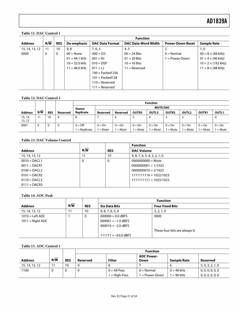
The AD1839A register map has eight registers that are used to control the functionality of the DAC section of the part. The function of the bits in these registers is discussed next.
Sample Rate These bits control the sample rate of the DACs. Based on a 24.576 MHz IMCLK, sample rates of 48 kHz, 96 kHz, and 192 kHz are available. The MCLK scaling bits in ADC Control 3 should be programmed appropriately, based on the master clock frequency.
Power-Down/Reset This bit controls the power-down status of the DAC section. By default, normal mode is selected; by setting this bit, the digital section of the DAC stage can be put into a low power mode, thus reducing the digital current. The analog output section of the DAC stage is not powered down.
DAC Data-Word Width These two bits set the word width of the DAC data. Compact disk (CD) compatibility may require 16 bits, but many modern digital audio formats require 24-bit sample resolution.
DAC Data Format The AD1839A serial data interface can be configured to be compatible with a choice of popular interface formats, including I2S, LJ, RJ, or DSP modes. Details on these interface modes are provided in the Serial Data Ports—Data Format section.
De-emphasis The AD1839A provides built-in de-emphasis filtering for the three standard sample rates of 32.0 kHz, 44.1 kHz, and 48 kHz.
Mute DAC Each of the six DACs in the AD1839A has its own independent mute control. Setting the appropriate bit mutes the DAC output. The AD1839A uses a clickless mute function that attenuates the output to approximately −100 dB over a number of cycles.
Stereo Replicate Setting this bit copies the digital data sent to the stereo pair DAC1 to the three other stereo DACs in the system. This allows all three stereo DACs to be driven by one digital data stream. Note that in this mode, DAC data sent to the other DACs is ignored.
DAC Volume Control Each DAC in the AD1839A has its own independent volume control. The volume of each DAC can be adjusted in 1,024 linear steps by programming the appropriate register. The default value for this register is 1023, which provides no attenuation, that is, full volume.
AD1839A
Rev. B | Page 20 of 24
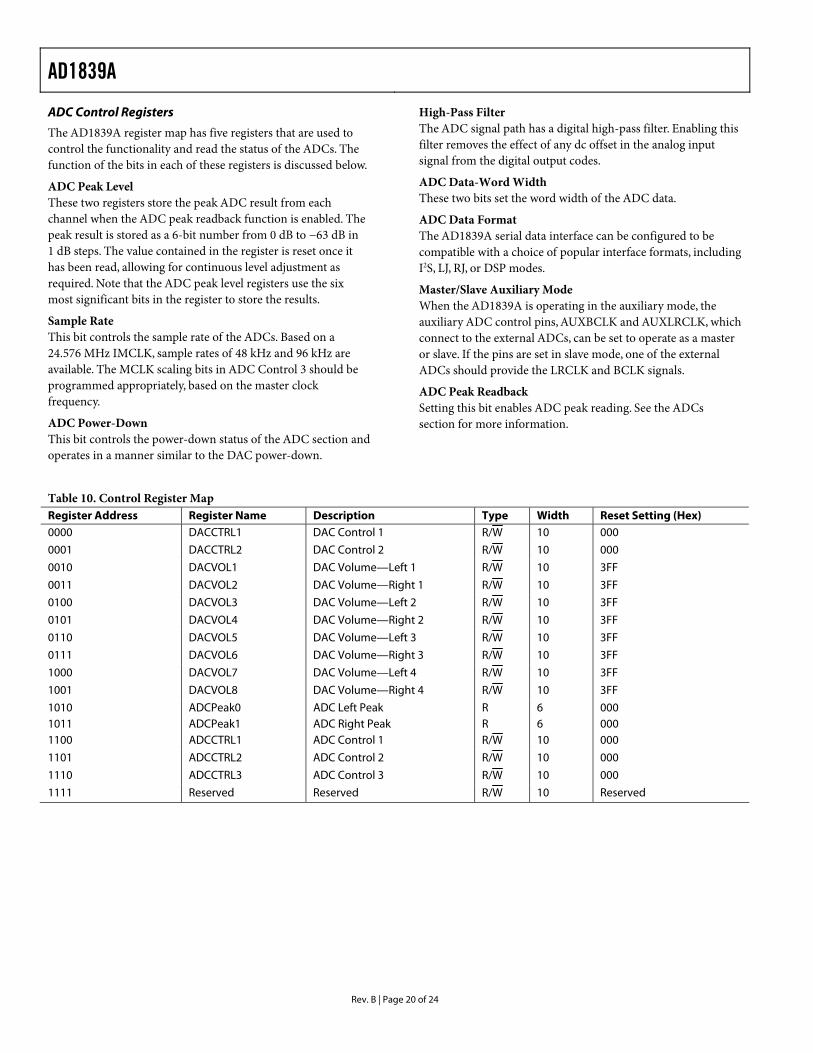
ADC Control Registers
The AD1839A register map has five registers that are used to control the functionality and read the status of the ADCs. The function of the bits in each of these registers is discussed below.
ADC Peak Level These two registers store the peak ADC result from each channel when the ADC peak readback function is enabled. The peak result is stored as a 6-bit number from 0 dB to −63 dB in 1 dB steps. The value contained in the register is reset once it has been read, allowing for continuous level adjustment as required. Note that the ADC peak level registers use the six most significant bits in the register to store the results.
Sample Rate This bit controls the sample rate of the ADCs. Based on a 24.576 MHz IMCLK, sample rates of 48 kHz and 96 kHz are available. The MCLK scaling bits in ADC Control 3 should be programmed appropriately, based on the master clock frequency.
ADC Power-Down This bit controls the power-down status of the ADC section and operates in a manner similar to the DAC power-down.
High-Pass Filter The ADC signal path has a digital high-pass filter. Enabling this filter removes the effect of any dc offset in the analog input signal from the digital output codes.
ADC Data-Word Width These two bits set the word width of the ADC data.
ADC Data Format The AD1839A serial data interface can be configured to be compatible with a choice of popular interface formats, including I2S, LJ, RJ, or DSP modes.
Master/Slave Auxiliary Mode When the AD1839A is operating in the auxiliary mode, the auxiliary ADC control pins, AUXBCLK and AUXLRCLK, which connect to the external ADCs, can be set to operate as a master or slave. If the pins are set in slave mode, one of the external ADCs should provide the LRCLK and BCLK signals.
ADC Peak Readback Setting this bit enables ADC peak reading. See the ADCs section for more information.
Table 10. Control Register Map Register Address Register Name Description Type Width Reset Setting (Hex) 0000 DACCTRL1 DAC Control 1 R/W 10 000
0001 DACCTRL2 DAC Control 2 R/W 10 000
0010 DACVOL1 DAC Volume—Left 1 R/W 10 3FF
0011 DACVOL2 DAC Volume—Right 1 R/W 10 3FF
0100 DACVOL3 DAC Volume—Left 2 R/W 10 3FF
0101 DACVOL4 DAC Volume—Right 2 R/W 10 3FF
0110 DACVOL5 DAC Volume—Left 3 R/W 10 3FF
0111 DACVOL6 DAC Volume—Right 3 R/W 10 3FF
1000 DACVOL7 DAC Volume—Left 4 R/W 10 3FF
1001 DACVOL8 DAC Volume—Right 4 R/W 10 3FF
1010 ADCPeak0 ADC Left Peak R 6 000 1011 ADCPeak1 ADC Right Peak R 6 000 1100 ADCCTRL1 ADC Control 1 R/W 10 000
1101 ADCCTRL2 ADC Control 2 R/W 10 000
1110 ADCCTRL3 ADC Control 3 R/W 10 000
1111 Reserved Reserved R/W 10 Reserved
AD1839A
Rev. B | Page 21 of 24
Table 11. DAC Control 1 Function Address R/W RES De-emphasis DAC Data Format DAC Data-Word Width Power-Down Reset Sample Rate
15, 14, 13, 12 11 10 9, 8 7, 6, 5 4, 3 2 1, 0 0000 0 0 00 = None 000 = I2S 00 = 24 Bits 0 = Normal 00 = 8 × (48 kHz) 01 = 44.1 kHz 001 = RJ 01 = 20 Bits 1 = Power-Down 01 = 4 × (96 kHz) 10 = 32.0 kHz 010 = DSP 10 = 16 Bits 10 = 2 × (192 kHz) 11 = 48.0 kHz 011 = LJ 11 = Reserved 11 = 8 × (48 kHz) 100 = Packed 256 101 = Packed128 110 = Reserved 111 = Reserved
Table 12. DAC Control 2 Function
MUTE DAC
Address R/W RES Reserved Stereo Replicate Reserved Reserved OUTR3 OUTL3 OUTR2 OUTL2 OUTR1 OUTL1
15, 14, 13, 12
11 10 9 8 7 6 5 4 3 2 1 0
0001 0 0 0 0 = Off 0 = On 0 = On 0 = On 0 = On 0 = On 0 = On 0 = On 0 = On 1 = Replicate 1 = Mute 1 = Mute 1 = Mute 1 = Mute 1 = Mute 1 = Mute 1 = Mute 1 = Mute
Table 13. DAC Volume Control Function
Address R/W RES DAC Volume 15, 14, 13, 12 11 10 9, 8, 7, 6, 5, 4, 3, 2, 1, 0 0010 = DACL1 0 0 0000000000 = Mute 0011 = DACR1 0000000001 = 1/1023 0100 = DACL2 0000000010 = 2/1023 0101 = DACR2 1111111110 = 1022/1023 0110 = DACL3 1111111111 = 1023/1023 0111 = DACR3
Table 14. ADC Peak Function
Address R/W RES Six Data Bits Four Fixed Bits 15, 14, 13, 12 11 10 9, 8, 7, 6, 5, 4 3, 2, 1, 0 1010 = Left ADC 1 0 000000 = 0.0 dBFS 0000 1011 = Right ADC 000001 = –1.0 dBFS 000010 = –2.0 dBFS These four bits are always 0. 111111 = –63.0 dBFS
Table 15. ADC Control 1 Function
Address R/W RES Reserved Filter ADC Power-Down Sample Rate Reserved
15, 14, 13, 12 11 10 9 8 7 6 5, 4, 3, 2, 1, 0 1100 0 0 0 0 = All Pass 0 = Normal 0 = 48 kHz 0, 0, 0, 0, 0, 0 1 = High-Pass 1 = Power-Down 1 = 96 kHz 0, 0, 0, 0, 0, 0
AD1839A
Rev. B | Page 22 of 24
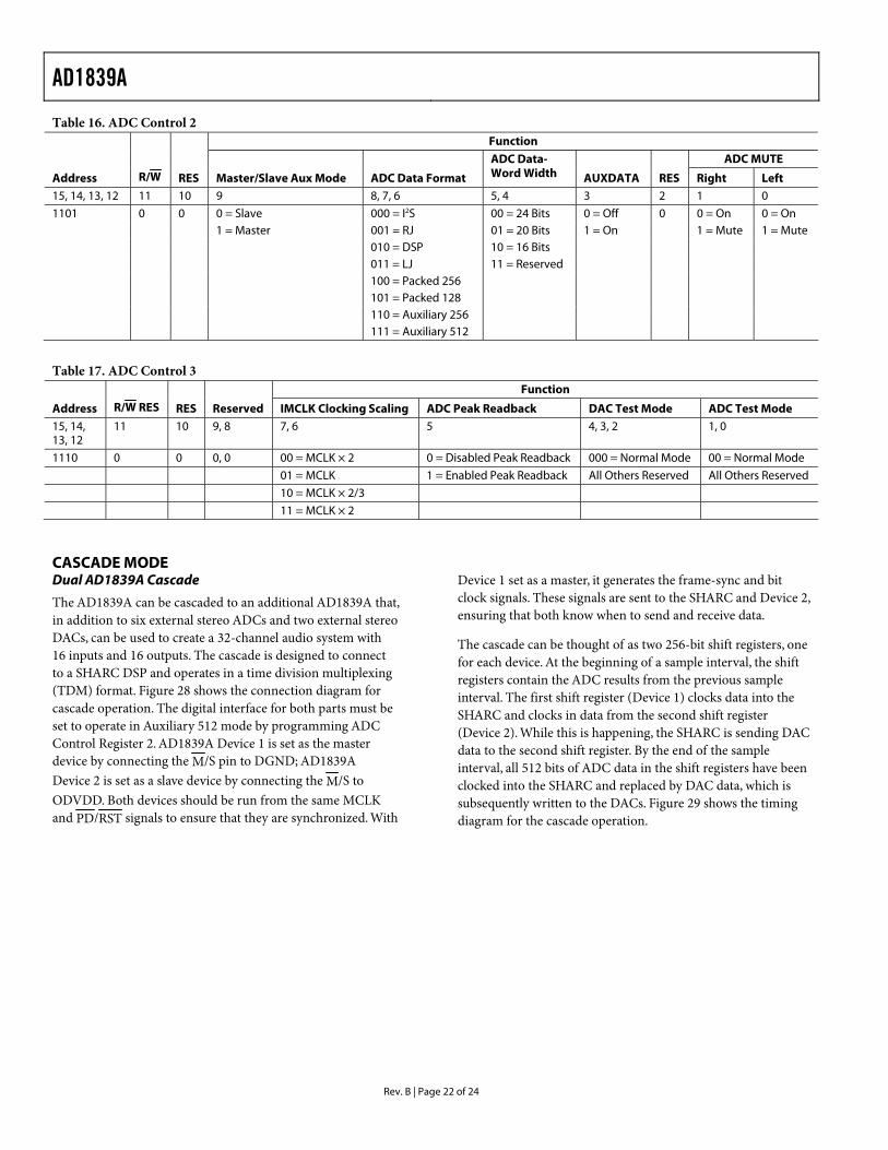
Table 16. ADC Control 2 Function
ADC MUTE
Address R/W RES Master/Slave Aux Mode ADC Data Format
ADC Data- Word Width AUXDATA RES Right Left
15, 14, 13, 12 11 10 9 8, 7, 6 5, 4 3 2 1 0
1101 0 0 0 = Slave 000 = I2S 00 = 24 Bits 0 = Off 0 0 = On 0 = On 1 = Master 001 = RJ 01 = 20 Bits 1 = On 1 = Mute 1 = Mute 010 = DSP 10 = 16 Bits 011 = LJ 11 = Reserved 100 = Packed 256 101 = Packed 128 110 = Auxiliary 256 111 = Auxiliary 512
Table 17. ADC Control 3 Function
Address R/W RES RES Reserved IMCLK Clocking Scaling ADC Peak Readback DAC Test Mode ADC Test Mode 15, 14, 13, 12
11 10 9, 8 7, 6 5 4, 3, 2 1, 0
1110 0 0 0, 0 00 = MCLK × 2 0 = Disabled Peak Readback 000 = Normal Mode 00 = Normal Mode
01 = MCLK 1 = Enabled Peak Readback All Others Reserved All Others Reserved
10 = MCLK × 2/3
11 = MCLK × 2
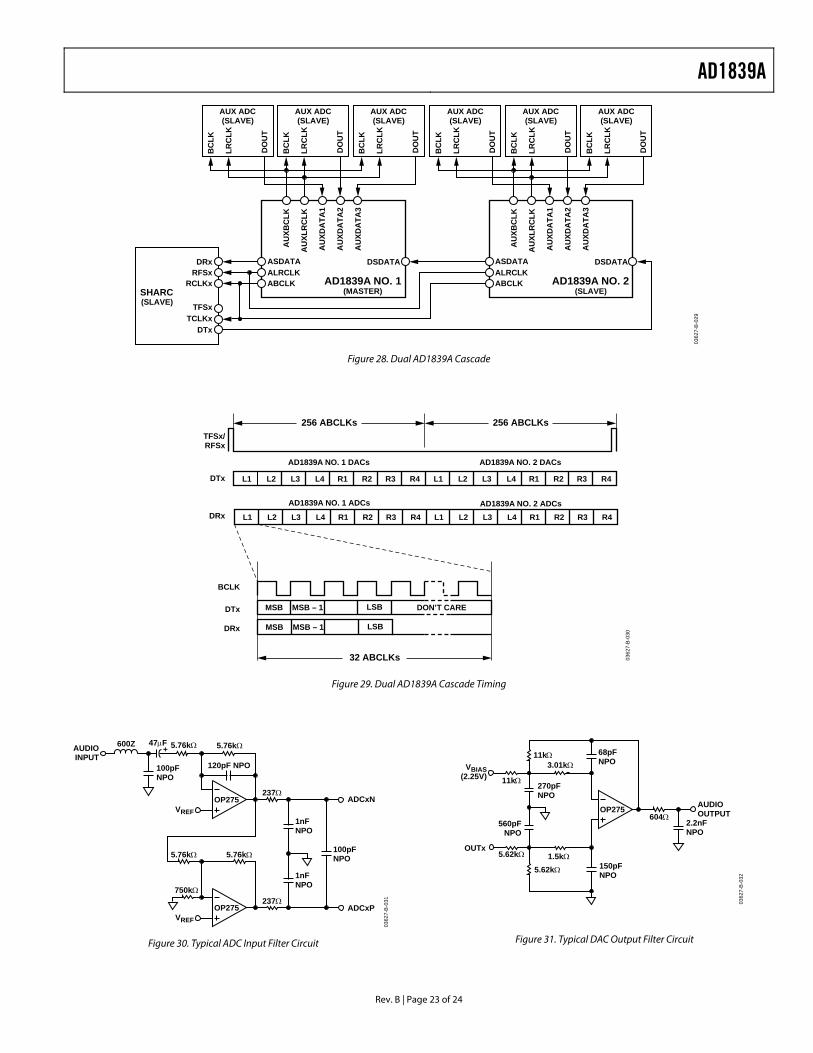
CASCADE MODE Dual AD1839A Cascade
The AD1839A can be cascaded to an additional AD1839A that, in addition to six external stereo ADCs and two external stereo DACs, can be used to create a 32-channel audio system with 16 inputs and 16 outputs. The cascade is designed to connect to a SHARC DSP and operates in a time division multiplexing (TDM) format. Figure 28 shows the connection diagram for cascade operation. The digital interface for both parts must be set to operate in Auxiliary 512 mode by programming ADC Control Register 2. AD1839A Device 1 is set as the master device by connecting the M/S pin to DGND; AD1839A Device 2 is set as a slave device by connecting the M/S to ODVDD. Both devices should be run from the same MCLK and PD/RST signals to ensure that they are synchronized. With
Device 1 set as a master, it generates the frame-sync and bit clock signals. These signals are sent to the SHARC and Device 2, ensuring that both know when to send and receive data.
The cascade can be thought of as two 256-bit shift registers, one for each device. At the beginning of a sample interval, the shift registers contain the ADC results from the previous sample interval. The first shift register (Device 1) clocks data into the SHARC and clocks in data from the second shift register (Device 2). While this is happening, the SHARC is sending DAC data to the second shift register. By the end of the sample interval, all 512 bits of ADC data in the shift registers have been clocked into the SHARC and replaced by DAC data, which is subsequently written to the DACs. Figure 29 shows the timing diagram for the cascade operation.
AD1839A
Rev. B | Page 23 of 24
ALRCLKABCLK
ASDATA DSDATA
AD1839A NO. 1(MASTER)SHARC
(SLAVE)
AUX ADC(SLAVE)
DO
UT
LRC
LK
BC
LKA
UXB
CLK
AU
XLR
CLK
AU
XDA
TA1
AU
XDA
TA2
AU
XDA
TA3
DRxRFSx
RCLKx
TCLKxDTx
TFSx
0362
7-B-
029
AUX ADC(SLAVE)
DO
UT
LRC
LK
BC
LK
AUX ADC(SLAVE)
DO
UT
LRC
LK
BC
LK
ALRCLKABCLK
ASDATA DSDATA
AD1839A NO. 2(SLAVE)
AUX ADC(SLAVE)
DO
UT
LRC
LK
BC
LKA
UXB
CLK
AU
XLR
CLK
AU
XDA
TA1
AU
XDA
TA2
AU
XDA
TA3
AUX ADC(SLAVE)
DO
UT
LRC
LK
BC
LK
AUX ADC(SLAVE)
DO
UT
LRC
LK
BC
LK
Figure 28. Dual AD1839A Cascade
AD1839A NO. 1 DACs
L1 L2 L3 L4 R1 R2 R3 R4
AD1839A NO. 2 DACs
L1 L2 L3 L4 R1 R2 R3 R4
TFSx/RFSx
DTx
AD1839A NO. 1 ADCs
L1 L2 L3 L4 R1 R2 R3 R4AD1839A NO. 2 ADCs
L1 L2 L3 L4 R1 R2 R3 R4DRx
MSB MSB – 1 LSB
BCLK
DTx
MSB MSB – 1 LSBDRx
DON’T CARE
0362
7-B-
030
256 ABCLKs
32 ABCLKs
256 ABCLKs
Figure 29. Dual AD1839A Cascade Timing
5.76kΩ
100pFNPO
AUDIOINPUT
600Z +47µF 5.76kΩ
120pF NPO
5.76kΩ 5.76kΩ
750kΩ
1nFNPO
237Ω
1nFNPO
100pFNPO
ADCxP
ADCxN
0362
7-B-
031
OP275
VREF
VREF
OP275237Ω
Figure 30. Typical ADC Input Filter Circuit
3.01kΩ
11kΩ 270pFNPO
560pFNPO
68pFNPO
11kΩ
150pFNPO
1.5kΩ5.62kΩ
5.62kΩ
604Ω2.2nFNPO
VBIAS(2.25V)
OUTx
AUDIOOUTPUTOP275
0362
7-B-
032
Figure 31. Typical DAC Output Filter Circuit
AD1839A
Rev. B | Page 24 of 24
OUTLINE DIMENSIONS
SEATINGPLANE
VIEW A
2.45MAX
1.030.880.73
TOP VIEW(PINS DOWN)
1
3940
1314
2726
52PIN 1
0.65 BSC
13.4513.20 SQ12.95
7.80REF
10.2010.00 SQ 9.80
0.400.22
7°0°
2.202.001.80
0.13 MINCOPLANARITY
0.25MAX
10°6°2° 0.23
0.11
COMPLIANT TO JEDEC STANDARDS MS-022-AC.
VIEW AROTATED 90° CCW
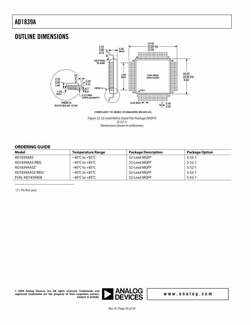
Figure 32. 52-Lead Metric Quad Flat Package [MQFP] (S-52-1)
Dimensions shown in millimeters
ORDERING GUIDE Model Temperature Range Package Description Package Option AD1839AAS −40°C to +85°C 52-Lead MQFP S-52-1 AD1839AAS-REEL −40°C to +85°C 52-Lead MQFP S-52-1 AD1839AASZ1 −40°C to +85°C 52-Lead MQFP S-52-1 AD1839AASZ-REEL1 −40°C to +85°C 52-Lead MQFP S-52-1 EVAL-AD1839AEB −40°C to +85°C 52-Lead MQFP S-52-1
1 Z = Pb-free part.
© 2004 Analog Devices, Inc. All rights reserved. Trademarks and registered trademarks are the property of their respective owners. C03627–0–6/04(B)
Recommended