Embed Size (px)
Citation preview

Zynq UltraScale+ MPSoC Processing System v3.1LogiCORE IP Product Guide
PG201 October 4, 2017

Zynq UltraScale+ MPSoC Processing System v3.1 2PG201 October 4, 2017 www.xilinx.com
Table of Contents
Chapter 1: Overview
Feature Summary. . . . . . . . . . . . . . . . . . . . . . . . . . . . . . . . . . . . . . . . . . . . . . . . . . . . . . . . . . . . . . . . . . 5
Unsupported Features and Known Limitations . . . . . . . . . . . . . . . . . . . . . . . . . . . . . . . . . . . . . . . . . . 5
Licensing and Ordering . . . . . . . . . . . . . . . . . . . . . . . . . . . . . . . . . . . . . . . . . . . . . . . . . . . . . . . . . . . . . 5
Chapter 2: Product Specification
Functional Description. . . . . . . . . . . . . . . . . . . . . . . . . . . . . . . . . . . . . . . . . . . . . . . . . . . . . . . . . . . . . . 6
Standards . . . . . . . . . . . . . . . . . . . . . . . . . . . . . . . . . . . . . . . . . . . . . . . . . . . . . . . . . . . . . . . . . . . . . . . 19
Performance. . . . . . . . . . . . . . . . . . . . . . . . . . . . . . . . . . . . . . . . . . . . . . . . . . . . . . . . . . . . . . . . . . . . . 20
Resource Utilization. . . . . . . . . . . . . . . . . . . . . . . . . . . . . . . . . . . . . . . . . . . . . . . . . . . . . . . . . . . . . . . 20
Port Descriptions . . . . . . . . . . . . . . . . . . . . . . . . . . . . . . . . . . . . . . . . . . . . . . . . . . . . . . . . . . . . . . . . . 20
Register Space . . . . . . . . . . . . . . . . . . . . . . . . . . . . . . . . . . . . . . . . . . . . . . . . . . . . . . . . . . . . . . . . . . . 21
Chapter 3: Designing with the Core
General Design Guidelines . . . . . . . . . . . . . . . . . . . . . . . . . . . . . . . . . . . . . . . . . . . . . . . . . . . . . . . . . 22
Interrupts . . . . . . . . . . . . . . . . . . . . . . . . . . . . . . . . . . . . . . . . . . . . . . . . . . . . . . . . . . . . . . . . . . . . . . . 22
Clocking. . . . . . . . . . . . . . . . . . . . . . . . . . . . . . . . . . . . . . . . . . . . . . . . . . . . . . . . . . . . . . . . . . . . . . . . . 22
Resets . . . . . . . . . . . . . . . . . . . . . . . . . . . . . . . . . . . . . . . . . . . . . . . . . . . . . . . . . . . . . . . . . . . . . . . . . . 23
Chapter 4: Design Flow Steps
Customizing and Generating the Core . . . . . . . . . . . . . . . . . . . . . . . . . . . . . . . . . . . . . . . . . . . . . . . . 24
PS Zynq UltraScale+ MPSoC Block Design . . . . . . . . . . . . . . . . . . . . . . . . . . . . . . . . . . . . . . . . . . . . . 27
I/O Configuration . . . . . . . . . . . . . . . . . . . . . . . . . . . . . . . . . . . . . . . . . . . . . . . . . . . . . . . . . . . . . . . . . 28
Clock Configuration . . . . . . . . . . . . . . . . . . . . . . . . . . . . . . . . . . . . . . . . . . . . . . . . . . . . . . . . . . . . . . . 30
Fractional Clocking. . . . . . . . . . . . . . . . . . . . . . . . . . . . . . . . . . . . . . . . . . . . . . . . . . . . . . . . . . . . . . . . 36
DDR Configuration . . . . . . . . . . . . . . . . . . . . . . . . . . . . . . . . . . . . . . . . . . . . . . . . . . . . . . . . . . . . . . . . 37
PS-PL Configuration . . . . . . . . . . . . . . . . . . . . . . . . . . . . . . . . . . . . . . . . . . . . . . . . . . . . . . . . . . . . . . . 40
Advanced Configuration . . . . . . . . . . . . . . . . . . . . . . . . . . . . . . . . . . . . . . . . . . . . . . . . . . . . . . . . . . . 43
PCIe Configuration . . . . . . . . . . . . . . . . . . . . . . . . . . . . . . . . . . . . . . . . . . . . . . . . . . . . . . . . . . . . . . . . 46
Isolation Configurations . . . . . . . . . . . . . . . . . . . . . . . . . . . . . . . . . . . . . . . . . . . . . . . . . . . . . . . . . . . 47
User Parameters. . . . . . . . . . . . . . . . . . . . . . . . . . . . . . . . . . . . . . . . . . . . . . . . . . . . . . . . . . . . . . . . . . 54
Output Generation. . . . . . . . . . . . . . . . . . . . . . . . . . . . . . . . . . . . . . . . . . . . . . . . . . . . . . . . . . . . . . . . 55
Constraining the Core . . . . . . . . . . . . . . . . . . . . . . . . . . . . . . . . . . . . . . . . . . . . . . . . . . . . . . . . . . . . . 55
Simulation . . . . . . . . . . . . . . . . . . . . . . . . . . . . . . . . . . . . . . . . . . . . . . . . . . . . . . . . . . . . . . . . . . . . . . 56
Synthesis and Implementation . . . . . . . . . . . . . . . . . . . . . . . . . . . . . . . . . . . . . . . . . . . . . . . . . . . . . . 56
Send Feedback

Zynq UltraScale+ MPSoC Processing System v3.1 3PG201 October 4, 2017 www.xilinx.com
Chapter 5: Example Design
Appendix A: Upgrading
Upgrading in the Vivado Design Suite . . . . . . . . . . . . . . . . . . . . . . . . . . . . . . . . . . . . . . . . . . . . . . . . 65
Appendix B: Port Descriptions
Appendix C: User Parameters
Appendix D: Debugging
Finding Help on Xilinx.com . . . . . . . . . . . . . . . . . . . . . . . . . . . . . . . . . . . . . . . . . . . . . . . . . . . . . . . . 194
Documentation . . . . . . . . . . . . . . . . . . . . . . . . . . . . . . . . . . . . . . . . . . . . . . . . . . . . . . . . . . . . . . . . . 194
Solution Centers. . . . . . . . . . . . . . . . . . . . . . . . . . . . . . . . . . . . . . . . . . . . . . . . . . . . . . . . . . . . . . . . . 194
Answer Records . . . . . . . . . . . . . . . . . . . . . . . . . . . . . . . . . . . . . . . . . . . . . . . . . . . . . . . . . . . . . . . . . 195
Technical Support . . . . . . . . . . . . . . . . . . . . . . . . . . . . . . . . . . . . . . . . . . . . . . . . . . . . . . . . . . . . . . . 195
Appendix E: Additional Resources and Legal Notices
Xilinx Resources . . . . . . . . . . . . . . . . . . . . . . . . . . . . . . . . . . . . . . . . . . . . . . . . . . . . . . . . . . . . . . . . . 196
Documentation Navigator and Design Hubs . . . . . . . . . . . . . . . . . . . . . . . . . . . . . . . . . . . . . . . . . . 196
References . . . . . . . . . . . . . . . . . . . . . . . . . . . . . . . . . . . . . . . . . . . . . . . . . . . . . . . . . . . . . . . . . . . . . 197
Revision History . . . . . . . . . . . . . . . . . . . . . . . . . . . . . . . . . . . . . . . . . . . . . . . . . . . . . . . . . . . . . . . . . 198
Notice of Disclaimer. . . . . . . . . . . . . . . . . . . . . . . . . . . . . . . . . . . . . . . . . . . . . . . . . . . . . . . . . . . . . . 200
Send Feedback
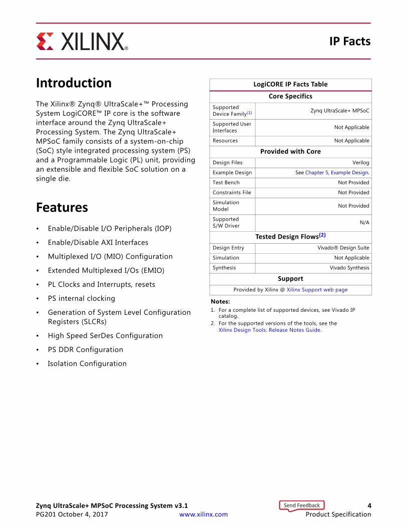
Zynq UltraScale+ MPSoC Processing System v3.1 4PG201 October 4, 2017 www.xilinx.com Product Specification
Introduction
The Xilinx® Zynq® UltraScale+™ Processing System LogiCORE™ IP core is the software interface around the Zynq UltraScale+ Processing System. The Zynq UltraScale+ MPSoC family consists of a system-on-chip (SoC) style integrated processing system (PS) and a Programmable Logic (PL) unit, providing an extensible and flexible SoC solution on a single die.
Features
• Enable/Disable I/O Peripherals (IOP)
• Enable/Disable AXI Interfaces
• Multiplexed I/O (MIO) Configuration
• Extended Multiplexed I/Os (EMIO)
• PL Clocks and Interrupts, resets
• PS internal clocking
• Generation of System Level Configuration Registers (SLCRs)
• High Speed SerDes Configuration
• PS DDR Configuration
• Isolation Configuration
IP Facts
LogiCORE IP Facts Table
Core Specifics
Supported Device Family(1) Zynq UltraScale+ MPSoC
Supported User Interfaces Not Applicable
Resources Not Applicable
Provided with Core
Design Files Verilog
Example Design See Chapter 5, Example Design.
Test Bench Not Provided
Constraints File Not Provided
Simulation Model Not Provided
Supported S/W Driver N/A
Tested Design Flows(2)
Design Entry Vivado® Design Suite
Simulation Not Applicable
Synthesis Vivado Synthesis
Support
Provided by Xilinx @ Xilinx Support web page
Notes: 1. For a complete list of supported devices, see Vivado IP
catalog.2. For the supported versions of the tools, see the
Xilinx Design Tools: Release Notes Guide.
Send Feedback
Zynq UltraScale+ MPSoC Processing System v3.1 5PG201 October 4, 2017 www.xilinx.com
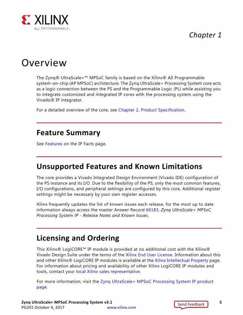
Chapter 1
OverviewThe Zynq® UltraScale+™ MPSoC family is based on the Xilinx® All Programmable system-on-chip (AP MPSoC) architecture. The Zynq UltraScale+ Processing System core acts as a logic connection between the PS and the Programmable Logic (PL) while assisting you to integrate customized and integrated IP cores with the processing system using the Vivado® IP integrator.
For a detailed overview of the core, see Chapter 2, Product Specification.
Feature SummarySee Features on the IP Facts page.
Unsupported Features and Known LimitationsThe core provides a Vivado Integrated Design Environment (Vivado IDE) configuration of the PS instance and its I/O. Due to the flexibility of the PS, only the most common features, I/O configurations, and peripheral settings are configured by this core. Additional register settings might be necessary by your own register accesses.
Xilinx frequently updates the list of known issues each release, for the most up to date information always access the master Answer Record 66183, Zynq UltraScale+ MPSoC Processing System IP - Release Notes and Known Issues.
Licensing and OrderingThis Xilinx® LogiCORE™ IP module is provided at no additional cost with the Xilinx® Vivado Design Suite under the terms of the Xilinx End User License. Information about this and other Xilinx® LogiCORE IP modules is available at the Xilinx Intellectual Property page. For information about pricing and availability of other Xilinx LogiCORE IP modules and tools, contact your local Xilinx sales representative.
For more information, visit the Zynq UltraScale+ MPSoC Processing System IP product page.
Send Feedback

Zynq UltraScale+ MPSoC Processing System v3.1 6PG201 October 4, 2017 www.xilinx.com
Chapter 2
Product Specification
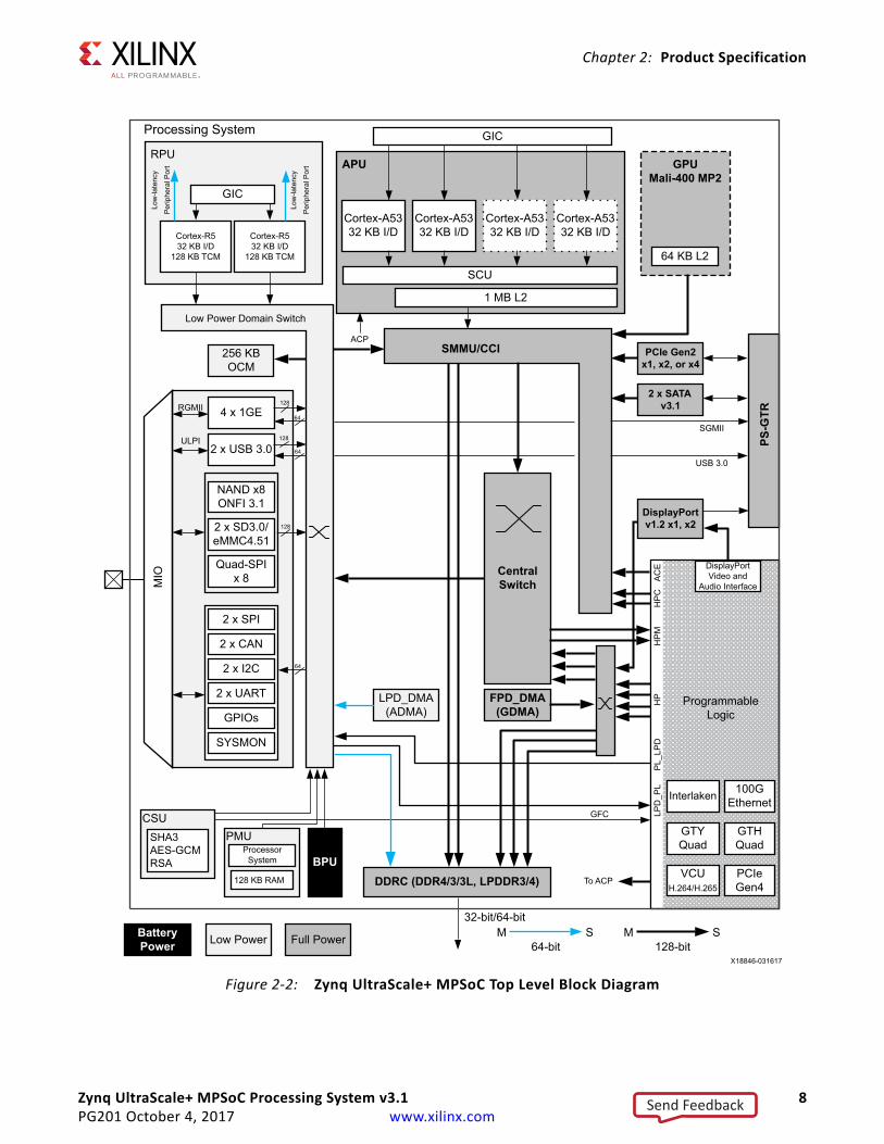
Functional DescriptionThe Zynq® UltraScale+™ MPSoC Processing System wrapper instantiates the processing system section of the Zynq UltraScale+ MPSoC for the programmable logic and external board logic. The wrapper includes unaltered connectivity and some logic functions for some signals. For a description of the architecture of the processing system, see the Zynq UltraScale All Programmable MPSoC Technical Reference Manual (UG1085) [Ref 1]. Figure 2-1 shows the architecture of Processing System (PS) IP wrapper.
X-Ref Target - Figure 2-1
Figure 2‐1: PS IP Wrapper Architecture
Send Feedback

Zynq UltraScale+ MPSoC Processing System v3.1 7PG201 October 4, 2017 www.xilinx.com
Chapter 2: Product Specification
The core connects the interface signals with the rest of the embedded system in the programmable logic. The interfaces between the processing system and programmable logic mainly consist of three main groups: the extended multiplexed I/O (EMIO), programmable logic I/O, and the AXI I/O groups. The PS Configuration Wizard (PCW) configures the Zynq UltraScale+ MPSoC Processing System Core. Double click PS IP on the Vivado® IPI (Inter-Process Interrupts) canvas to access the PCW. Figure 2-2 shows the PCW configuration on Zynq UltraScale+ MPSoC Processing System. The core performs the functions described in the following subsections.
Figure 2-2 shows a top-level block diagram.
Send Feedback
Zynq UltraScale+ MPSoC Processing System v3.1 8PG201 October 4, 2017 www.xilinx.com
Chapter 2: Product Specification
X-Ref Target - Figure 2-2
Figure 2‐2: Zynq UltraScale+ MPSoC Top Level Block Diagram
RPU
256 KBOCM
LPD_DMA(ADMA)
CSUPMU
Processing System
Cortex-R532 KB I/D
128 KB TCM
Cortex-R532 KB I/D
128 KB TCM
4 x 1GE
APU
Cortex-A5332 KB I/D
Cortex-A5332 KB I/D
Cortex-A5332 KB I/D
Cortex-A5332 KB I/D
GIC
SCU
1 MB L2
GPUMali-400 MP2
64 KB L2
2 x USB 3.0
NAND x8ONFI 3.1
2 x SD3.0/eMMC4.51
Quad-SPIx 8
2 x SPI
2 x CAN
2 x I2C
2 x UART
GPIOs
SYSMON
MIO Central
Switch
FPD_DMA (GDMA)
VCU H.264/H.265
PCIe Gen4
DisplayPort v1.2 x1, x2
2 x SATAv3.1
PCIe Gen2x1, x2, or x4
SHA3AES-GCMRSA
Processor System BPU
DDRC (DDR4/3/3L, LPDDR3/4)
Programmable Logic
128 KB RAM
PL_
LPD
HP
GIC
RGMII
ULPI PS-G
TR
SMMU/CCI
GFC
USB 3.0
SGMII
Low Power Domain Switch
To ACP
Low Power Full PowerBattery Power
32-bit/64-bit
64-bitM S
128-bitM S
LPD
_PL
HP
CH
PM
GTY Quad
GTH Quad
Interlaken 100G Ethernet
AC
E DisplayPort Video and
Audio Interface
Low
-late
ncy
Per
iphe
ral P
ort
Low
-late
ncy
Per
iphe
ral P
ort
ACP
128
128
64
64
64
128
Send Feedback
Zynq UltraScale+ MPSoC Processing System v3.1 9PG201 October 4, 2017 www.xilinx.com
Chapter 2: Product Specification
Connectivity
ddr, mio, por/clk/srst ports are unaltered.
• fclk are also made of individual signals instead of the array FCLKCLK (3:0).
• PS PL IRQ are made of individual signals ps_pl_irq_can0, ps_pl_irq_can1, ps_pl_irq_enet0, ps_pl_irq_enet1, ps_pl_irq_enet2, ps_pl_irq_enet3, ps_pl_irq_enet0_wake0, ps_pl_irq_enet0_wake1, ps_pl_irq_enet0_wake2, ps_pl_irq_enet0_wake3, ps_pl_irq_gpio, ps_pl_irq_i2c0, ps_pl_irq_i2c1, ps_pl_irq_uart0, ps_pl_irq_uart1, ps_pl_irq_sdio0, ps_pl_irq_sdio1, ps_pl_irq_sdio0_wake, ps_pl_irq_sdio1_wake, ps_pl_irq_spi0, ps_pl_irq_spi1, ps_pl_irq_qspi, ps_pl_irq_ttc0_0, ps_pl_irq_ttc0_1, ps_pl_irq_ttc0_2, ps_pl_irq_ttc1_0, ps_pl_irq_ttc1_1, ps_pl_irq_ttc1_2, ps_pl_irq_ttc2_0, ps_pl_irq_ttc2_1, ps_pl_irq_ttc2_2, ps_pl_irq_ttc3_0, ps_pl_irq_ttc3_1, ps_pl_irq_ttc3_2, ps_pl_irq_csu_pmu_wdt, ps_pl_irq_lp_wdt, ps_pl_irq_usb3_0_endpoint, ps_pl_irq_usb3_0_otg, ps_pl_irq_usb3_1_endpoint, ps_pl_irq_usb3_1_otg, ps_pl_irq_adma(1)_chan, ps_pl_irq_usb3_0_pmu_wakeup, ps_pl_irq_gdma(2)_chan, ps_pl_irq_csu, ps_pl_irq_csu_dma, ps_pl_irq_efuse, ps_pl_irq_xmpu_lpd, ps_pl_irq_ddr_ss, ps_pl_irq_nand, ps_pl_irq_fp_wdt, ps_pl_irq_pcie_msi, ps_pl_irq_pcie_legacy, ps_pl_irq_pcie_dma, ps_pl_irq_pcie_msc, ps_pl_irq_dport, ps_pl_irq_fpd_apb_int, ps_pl_irq_fpd_atb_error, ps_pl_irq_dpdma, ps_pl_irq_apm_fpd, ps_pl_irq_gpu, ps_pl_irq_sata, ps_pl_irq_xmpu_fpd, ps_pl_irq_apu_cpumnt, ps_pl_irq_apu_cti, ps_pl_irq_apu_pmu, ps_pl_irq_apu_comm, ps_pl_irq_apu_l2err, ps_pl_irq_apu_exterr, ps_pl_irq_apu_regs, ps_pl_irq_intf_ppd_cci, ps_pl_irq_intf_fpd_smmu, ps_pl_irq_atb_err_lpd, ps_pl_irq_aib_axi, ps_pl_irq_ams, ps_pl_irq_lpd_apm ps_pl_irq_rtc_alaram, ps_pl_irq_rtc_seconds, ps_pl_irq_clkmon, ps_pl_irq_ipi_channel0,ps_pl_irq_ipi_channel1,ps_pl_irq_ipi_channnel2,ps_pl_irq_ipi_channnel7,ps_pl_irq_ipi_channnel8,ps_pl_irq_ipi_channnel9,ps_pl_irq_ipi_channnel10,ps_pl_irq_rpu_pm, ps_pl_irq_ocm_error, ps_pl_irq_lpd_apb_intr, ps_pl_irq_r5_core0_ecc_error, and ps_pl_irq_r5_core1_ecc_error.
• spi or spi* sson are made of individual signals spi*_ss2_o, spi*_ss1_o, and spi*_ss_o.
Notes: 1. ADMA is also referenced as LPD_DMA throughout this guide. These two terms are synonymous.2. GDMA is also referenced as FPD_DMA throughout this guide. These two terms are synonymous.
I/O Peripherals
I/O Peripherals (IOP) include the following.
• Quad serial peripheral interface (SPI) flash memory
• NAND flash
• UART
• I2C
Send Feedback
Zynq UltraScale+ MPSoC Processing System v3.1 10PG201 October 4, 2017 www.xilinx.com
Chapter 2: Product Specification
• SPI flash memory
• Secure Digital Input Output (SDIO)
• general purpose I/O (GPIO)
• controller area network (CAN)
• USB
• Ethernet
The interfaces for these I/O peripherals (IOPs) can be routed to MIO ports and the extended multiplexed I/O (EMIO) interfaces as described in the Zynq UltraScale All Programmable MPSoC Technical Reference Manual (UG1085) [Ref 1].
• Low power domain (LPD) peripherals available in PS:
° 4 X Gigabit Ethernet
° 2 X USB3
° 2 X SDIO
° 2 X SPI
° 2 X CAN
° 2 X I2C
° 2 X UART
° NAND Controller
° Quad SPI flash memory
° Controller, GPIOs
° System Monitor
• Full power domain (FPD) peripherals available in PS:
° PCIe® Gen2
° 2 X Serial Advanced Technology Attachment (SATA)
° Display Port V1.2
MIO Ports
The Zynq UltraScale+ MPSoC design tools are used to configure the core MIO ports. There are up to 78 MIO ports available from the processing system. The wizard allows you to choose the peripheral ports to be connected to MIO ports.
Send Feedback
Zynq UltraScale+ MPSoC Processing System v3.1 11PG201 October 4, 2017 www.xilinx.com
Chapter 2: Product Specification
Extended MIO Ports
Because there are only up to 78 MIO available ports, many peripheral I/O ports beyond these can still be routed to the programmable logic through the Extended MIO (EMIO) interface. Alternative routing for IOP interfaces through programmable logic enables you to take full advantage of the IOP available in the processing system.
The EMIO for I2C, SPI flash memory, Ethernet management data input/output (MDIO), ARM® JTAG (PJTAG), SDIO, GPIO 3-state enable signals are inverted in the Zynq UltraScale+ MPSoC Processing System core.
The Zynq UltraScale+ MPSoC Processing System core allows you to select GPIO up to 96 bits. The Zynq UltraScale+ MPSoC Processing System has control logic to adjust user-selected width to flow into processing system.
See MIO Voltage Standard in Chapter 4.
AXI4 I/O Compliant Interfaces
Following are the AMBA® AXI4 compliant interfaces:
• Three PS General Purpose Master interfaces user configurable as 32, 64, and 128 bits in width. The default width is 128.
• Seven PL General Purpose Master interfaces user configurable as 32, 64, and 128 bits in width. The default width is 128.
• A 128-bit PL Master AXI coherency extension (ACE) interface for coherent I/O to A53 L1 and L2 cache systems
• A 128-bit PL Master ACP interface to support L2 cache allocation from PL masters.Limited to 64-byte cache line transfers only
See PS-PL Configuration in Chapter 4.
Logic for Vivado Design Suite IP - Processing System Interface
The Zynq UltraScale+ MPSoC Processing System core allows you to add Vivado® IP cores in the programmable logic to interface with the processing system. Custom direct memory access (DMA) functions can be implemented in the PL to oversee data movement irrespective of the processor intervention.
Send Feedback

Zynq UltraScale+ MPSoC Processing System v3.1 12PG201 October 4, 2017 www.xilinx.com
Chapter 2: Product Specification
Programmable Logic Clocks and Interrupts
The interrupts from the processing system I/O peripherals (IOP) are routed to the PL and assert asynchronously to the fclk clocks.
The PL can asynchronously assert up to 20 interrupts to the PS.
• 16 interrupt signals are mapped to the interrupt controller as a peripheral interrupt where each interrupt signal is set to a priority level and mapped to one or both of the CPUs. To use more that one interrupt signal, use a Concat block in the Vivado IP integrator to automatically size the width of the interrupt vector.
• The remaining four PL interrupt signals are inverted and routed to the nFIQ and nIRQ interrupt directly to the signals to the private peripheral interrupt (PPI) unit of the interrupt controller. There is an nFIQ and nIRQ interrupt for each of two CPUs.
The PS to PL, and PL to PS interrupts are listed in Table 2-2. For details on the interrupt signals, see the Interrupts chapter in the Zynq UltraScale All Programmable MPSoC Technical Reference Manual (UG1085) [Ref 1].
See PS-PL Configuration in Chapter 4 for Vivado Design Suite implementation.
Table 2‐1: Pin mapping to Interrupt IDs
Interrupt ID Pin
121 pl_ps_irq0 [0]
122 pl_ps_irq0 [1]
123 pl_ps_irq0 [2]
124 pl_ps_irq0 [3]
125 pl_ps_irq0 [4]
126 pl_ps_irq0 [5]
127 pl_ps_irq0 [6]
128 pl_ps_irq0 [7]
137 pl_ps_irq1 [0]
138 pl_ps_irq1 [1]
139 pl_ps_irq1 [2]
140 pl_ps_irq1 [3]
141 pl_ps_irq1 [4]
142 pl_ps_irq1 [5]
143 pl_ps_irq1 [6]
144 pl_ps_irq1 [7]
Send Feedback

Zynq UltraScale+ MPSoC Processing System v3.1 13PG201 October 4, 2017 www.xilinx.com
Chapter 2: Product Specification
Table 2‐2: Interrupt Map for PS Configuration Wizard (PCW)
S.No Interrupt ID Interrupt Name Description Type
PL-PS Interrupts (Interrupts that go from PL to PS)
1
121-128, 136-143
(See Table 2-1 for Pin mapping
to each interrupt ID)
IRQ-F2P[15:0]Shared Interrupts from PL logic to GICs of real-time processing unit (RPU) or application processing unit (APU)
Shared Interrupts
2 31 A53-Core_0 nIRQ Cortex™ A53 Core0 Private Peripheral Legacy IRQ Interrupt
Private Peripheral Interrupt
3 31 A53-Core_1 nIRQ Cortex A53 Core1 Private Peripheral Legacy IRQ Interrupt
Private Peripheral Interrupt
4 31 A53-Core_2 nIRQ Cortex A53 Core2 Private Peripheral Legacy IRQ Interrupt
Private Peripheral Interrupt
5 31 A53-Core_3 nIRQ Cortex A53 Core3 Private Peripheral Legacy IRQ Interrupt
Private Peripheral Interrupt
6 28 A53-Core_0 nFIQ Cortex A53 Core0 Private Peripheral Legacy FIQ Interrupt
Private Peripheral Interrupt
7 28 A53-Core_1 nFIQ Cortex A53 Core1 Private Peripheral Legacy FIQ Interrupt
Private Peripheral Interrupt
8 28 A53-Core_2 nFIQ Cortex A53 Core2 Private Peripheral Legacy FIQ Interrupt
Private Peripheral Interrupt
9 28 A53-Core_3 nFIQ Cortex A53 Core3 Private Peripheral Legacy FIQ Interrupt
Private Peripheral Interrupt
PS -PL Interrupts (Interrupts coming from PS to PL)
1 1 IRQ_P2F_RPU Performance Monitor 0 RPU Performance Monitor 0 Interrupt Shared
Interrupt
2 1 IRQ_P2F_RPU Performance Monitor 1 RPU Performance Monitor 1 Interrupt Shared
Interrupt
3 1 IRQ_P2F_OCM Error On-chip RAM (OCM) Error Interrupt Shared Interrupt
4 1 IRQ_P2F_LPD APB Interrupts
OR of all AMBA peripheral bus (APB) interrupts from LPD. Refer to the technical reference manual for APB Interrupt and Register Information.
Shared Interrupt
Send Feedback

Zynq UltraScale+ MPSoC Processing System v3.1 14PG201 October 4, 2017 www.xilinx.com
Chapter 2: Product Specification
5 1 IRQ_P2F_R5 Core0_ECC _Error
RPU CPU0 error-correction code
(ECC) errors interrupt. All ECC interrupts of CPU0 are combined into this interrupt.
Shared Interrupt
6 1 IRQ_P2F_R5 Core1_ECC_Error
RPU CPU1 ECC errors interrupt. All ECC interrupts of CPU1 are combined into this interrupt.
Shared Interrupt
7 1 IRQ_P2F_NAND NAND/NOR/SRAM Static Memory Controller Interrupt
Shared Interrupt
8 1 IRQ_P2F_QSPI SPI flash memory interrupt Shared Interrupt
9 1 IRQ_P2F_GPIO GPIO interrupt Shared Interrupt
10 1 IRQ_P2F_I2C0 I2C0 interrupt Shared Interrupt
11 1 IRQ_P2F_I2C1 I2C1 interrupt Shared Interrupt
12 1 IRQ_P2F_SPI0 SPI0 interrupt Shared Interrupt
13 1 IRQ_P2F_SPI1 SPI1 interrupt Shared Interrupt
14 1 IRQ_P2F_UART0 UART0 interrupt Shared Interrupt
15 1 IRQ_P2F_UART1 UART1 interrupt Shared Interrupt
16 1 IRQ_P2F_CAN0 CAN0 interrupt Shared Interrupt
17 1 IRQ_P2F_CAN1 CAN1 interrupt Shared Interrupt
18 1 IRQ_P2F_LPD_APM Or of all LPD AXI performance monitors (APMs)
Shared Interrupt
19 1 IRQ_P2F_RTC_ALARM RTC Alarm Interrupt Shared Interrupt
20 1 IRQ_P2F_RTC_SECONDS RTC Seconds Interrupt Shared Interrupt
21 1 IRQ_P2F_CLKMON Clock monitor coming from CRL Shared Interrupt
22 1 S_PL_IRQ_IPI_CHANNEL0OR' of all of inter-processor interrupt (IPIs)
targeted to IPI channel 0
Shared Interrupt
23 1 S_PL_IRQ_IPI_CHANNEL1OR' of all of inter-processor interrupt (IPIs)
targeted to IPI channel 1
Shared Interrupt
Table 2‐2: Interrupt Map for PS Configuration Wizard (PCW) (Cont’d)
S.No Interrupt ID Interrupt Name Description Type
Send Feedback

Zynq UltraScale+ MPSoC Processing System v3.1 15PG201 October 4, 2017 www.xilinx.com
Chapter 2: Product Specification
24 1 S_PL_IRQ_IPI_CHANNEL2OR' of all of inter-processor interrupt (IPIs)
targeted to IPI channel 2
Shared Interrupt
25 1 S_PL_IRQ_IPI_CHANNEL7OR' of all of inter-processor interrupt (IPIs)
targeted to IPI channel 7
Shared Interrupt
26 1 S_PL_IRQ_IPI_CHANNEL8OR' of all of inter-processor interrupt (IPIs)
targeted to IPI channel 8
Shared Interrupt
27 1 S_PL_IRQ_IPI_CHANNEL9OR' of all of inter-processor interrupt (IPIs)
targeted to IPI channel 9
Shared Interrupt
28 1 S_PL_IRQ_IPI_CHANNEL10OR' of all of inter-processor interrupt (IPIs)
targeted to IPI channel 10
Shared Interrupt
29 1 IRQ_P2F_TTC0_0 Triple Timer 0 Counter 0 Interrupt Shared Interrupt
30 1 IRQ_P2F_TTC0_1 Triple Timer 0 Counter 1 Interrupt Shared Interrupt
31 1 IRQ_P2F_TTC0_2 Triple Timer 0 Counter 2 Interrupt Shared Interrupt
32 1 IRQ_P2F_TTC1_0 Triple Timer 1 Counter 0 Interrupt Shared Interrupt
33 1 IRQ_P2F_TTC1_1 Triple Timer 1 Counter 1 Interrupt Shared Interrupt
34 1 IRQ_P2F_TTC1_2 Triple Timer 1 Counter 2 Interrupt Shared Interrupt
35 1 IRQ_P2F_TTC2_0 Triple Timer 2 Counter 0 Interrupt Shared Interrupt
36 1 IRQ_P2F_TTC2_1 Triple Timer 2 Counter 1 Interrupt Shared Interrupt
37 1 IRQ_P2F_TTC2_2 Triple Timer 2 Counter 2 Interrupt Shared Interrupt
38 1 IRQ_P2F_TTC3_0 Triple Timer 3 Counter 0 Interrupt Shared Interrupt
39 1 IRQ_P2F_TTC3_1 Triple Timer 3 Counter 1 Interrupt Shared Interrupt
40 1 IRQ_P2F_TTC3_2 Triple Timer 3 Counter 2 Interrupt Shared Interrupt
41 1 IRQ_P2F_SDIO0 SDIO0 interrupt Shared Interrupt
42 1 IRQ_P2F_SDIO1 SDIO1 interrupt Shared Interrupt
43 1 IRQ_P2F_SDIO0_wake SDIO0 wake interrupt Shared Interrupt
Table 2‐2: Interrupt Map for PS Configuration Wizard (PCW) (Cont’d)
S.No Interrupt ID Interrupt Name Description Type
Send Feedback
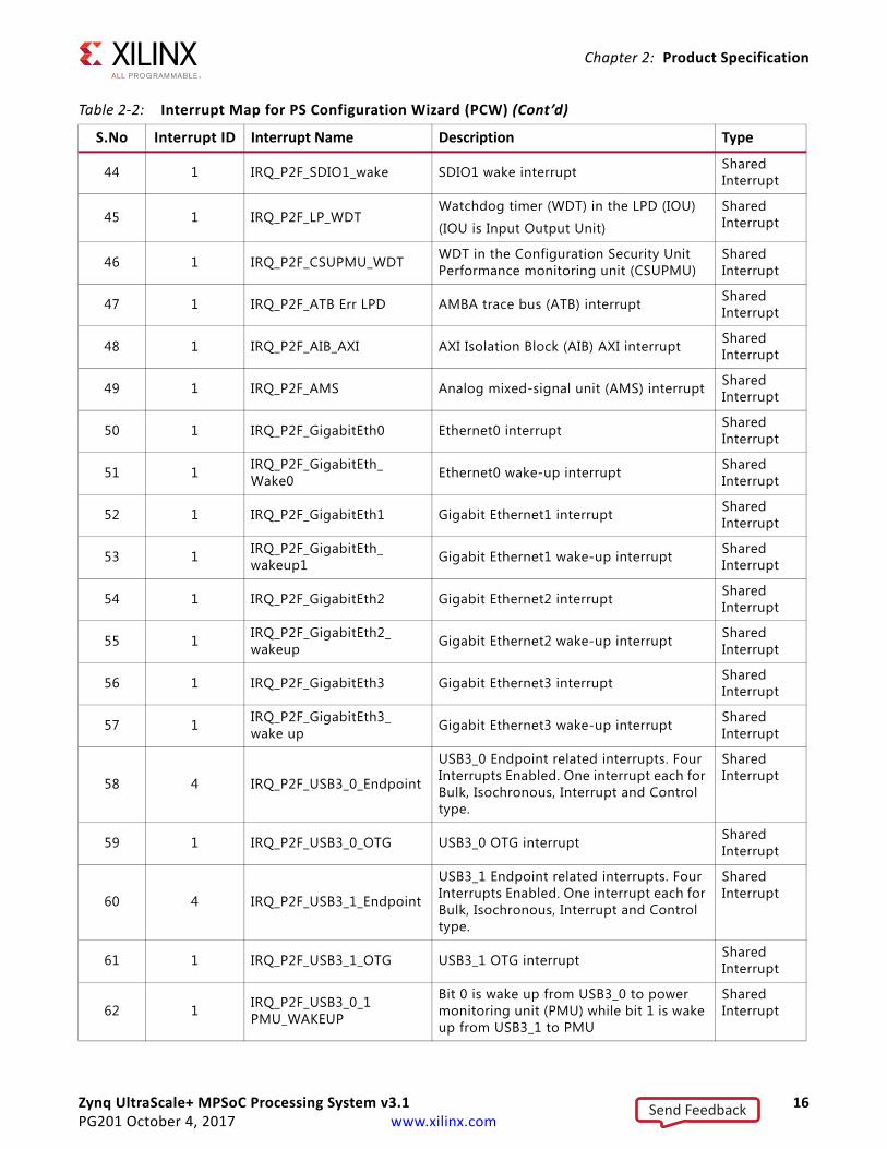
Zynq UltraScale+ MPSoC Processing System v3.1 16PG201 October 4, 2017 www.xilinx.com
Chapter 2: Product Specification
44 1 IRQ_P2F_SDIO1_wake SDIO1 wake interrupt Shared Interrupt
45 1 IRQ_P2F_LP_WDTWatchdog timer (WDT) in the LPD (IOU)
(IOU is Input Output Unit)
Shared Interrupt
46 1 IRQ_P2F_CSUPMU_WDT WDT in the Configuration Security Unit Performance monitoring unit (CSUPMU)
Shared Interrupt
47 1 IRQ_P2F_ATB Err LPD AMBA trace bus (ATB) interrupt Shared Interrupt
48 1 IRQ_P2F_AIB_AXI AXI Isolation Block (AIB) AXI interrupt Shared Interrupt
49 1 IRQ_P2F_AMS Analog mixed-signal unit (AMS) interrupt Shared Interrupt
50 1 IRQ_P2F_GigabitEth0 Ethernet0 interrupt Shared Interrupt
51 1 IRQ_P2F_GigabitEth_Wake0 Ethernet0 wake-up interrupt Shared
Interrupt
52 1 IRQ_P2F_GigabitEth1 Gigabit Ethernet1 interrupt Shared Interrupt
53 1 IRQ_P2F_GigabitEth_wakeup1 Gigabit Ethernet1 wake-up interrupt Shared
Interrupt
54 1 IRQ_P2F_GigabitEth2 Gigabit Ethernet2 interrupt Shared Interrupt
55 1 IRQ_P2F_GigabitEth2_wakeup Gigabit Ethernet2 wake-up interrupt Shared
Interrupt
56 1 IRQ_P2F_GigabitEth3 Gigabit Ethernet3 interrupt Shared Interrupt
57 1 IRQ_P2F_GigabitEth3_wake up Gigabit Ethernet3 wake-up interrupt Shared
Interrupt
58 4 IRQ_P2F_USB3_0_Endpoint
USB3_0 Endpoint related interrupts. Four Interrupts Enabled. One interrupt each for Bulk, Isochronous, Interrupt and Control type.
Shared Interrupt
59 1 IRQ_P2F_USB3_0_OTG USB3_0 OTG interrupt Shared Interrupt
60 4 IRQ_P2F_USB3_1_Endpoint
USB3_1 Endpoint related interrupts. Four Interrupts Enabled. One interrupt each for Bulk, Isochronous, Interrupt and Control type.
Shared Interrupt
61 1 IRQ_P2F_USB3_1_OTG USB3_1 OTG interrupt Shared Interrupt
62 1 IRQ_P2F_USB3_0_1 PMU_WAKEUP
Bit 0 is wake up from USB3_0 to power monitoring unit (PMU) while bit 1 is wake up from USB3_1 to PMU
Shared Interrupt
Table 2‐2: Interrupt Map for PS Configuration Wizard (PCW) (Cont’d)
S.No Interrupt ID Interrupt Name Description Type
Send Feedback

Zynq UltraScale+ MPSoC Processing System v3.1 17PG201 October 4, 2017 www.xilinx.com
Chapter 2: Product Specification
63 1 IRQ_P2F_ADMA(1)_Chan_0 LPD_DMA(ADMA) channel 0 interrupt Shared Interrupt
64 1 IRQ_P2F_ADMA(1)_Chan_1 LPD_DMA(ADMA) channel 1 interrupt Shared Interrupt
65 1 IRQ_P2F_ADMA(1)_Chan_2 LPD_DMA(ADMA) channel 2 interrupt Shared Interrupt
66 1 IRQ_P2F_ADMA(1)_Chan_3 LPD_DMA(ADMA) channel 3 interrupt Shared Interrupt
67 1 IRQ_P2F_ADMA(1)_Chan_4 LPD_DMA(ADMA) channel 4 interrupt Shared Interrupt
68 1 IRQ_P2F_ADMA(1)_Chan_5 LPD_DMA(ADMA) channel 5 interrupt Shared Interrupt
69 1 IRQ_P2F_ADMA(1)_Chan_6 LPD_DMA(ADMA) channel 6 interrupt Shared Interrupt
70 1 IRQ_P2F_ADMA(1)_Chan_7 LPD_DMA(ADMA) channel 7 interrupt Shared Interrupt
71 1 IRQ_P2F_CSU Device Configuration Module Interrupt Shared Interrupt
72 1 IRQ_P2F_CSU_DMA DMA for Configuration and Security Unit (CSU) interrupt
Shared Interrupt
73 1 IRQ_P2F_EFUSE EFUSE interrupt Shared Interrupt
74 1 IRQ_P2F_XMPU_LPDXilinx memory protection unit (XMPU) error Interrupt for OCM and LPD peripherals
Shared Interrupt
75 1 IRQ_P2F_DDR_SS DDR controller subsystem interrupt Shared Interrupt
76 1 IRQ_P2F_FP_WDT Top Level Watch Dog Timer Interrupt. Shared Interrupt
77 1 IRQ_P2F_PCIE_MSI
PCIE_MSI[0]=PCIe interrupt for MSI vectors 31 to 0
PCIE_MSI[1]=PCIe interrupt for MSI vectors 63 to 32
Shared Interrupt
78 1 IRQ_P2F_PCIE_Legacy PCIE legacy (INTA/BC/D) interrupts Shared Interrupt
79 1 IRQ_P2F_PCIE_DMA PCIE Bridge DMA interrupts Shared Interrupt
80 1 IRQ_P2F_PCIE_MSC PCIE misc (error etc) interrupts Shared Interrupt
81 1 IRQ_P2F_DPORT Display port general purpose interrupt Shared Interrupt
82 1 IRQ_P2F_FPD_APB_INT OR'd of all APB interrupts from LPD Shared Interrupt
Table 2‐2: Interrupt Map for PS Configuration Wizard (PCW) (Cont’d)
S.No Interrupt ID Interrupt Name Description Type
Send Feedback
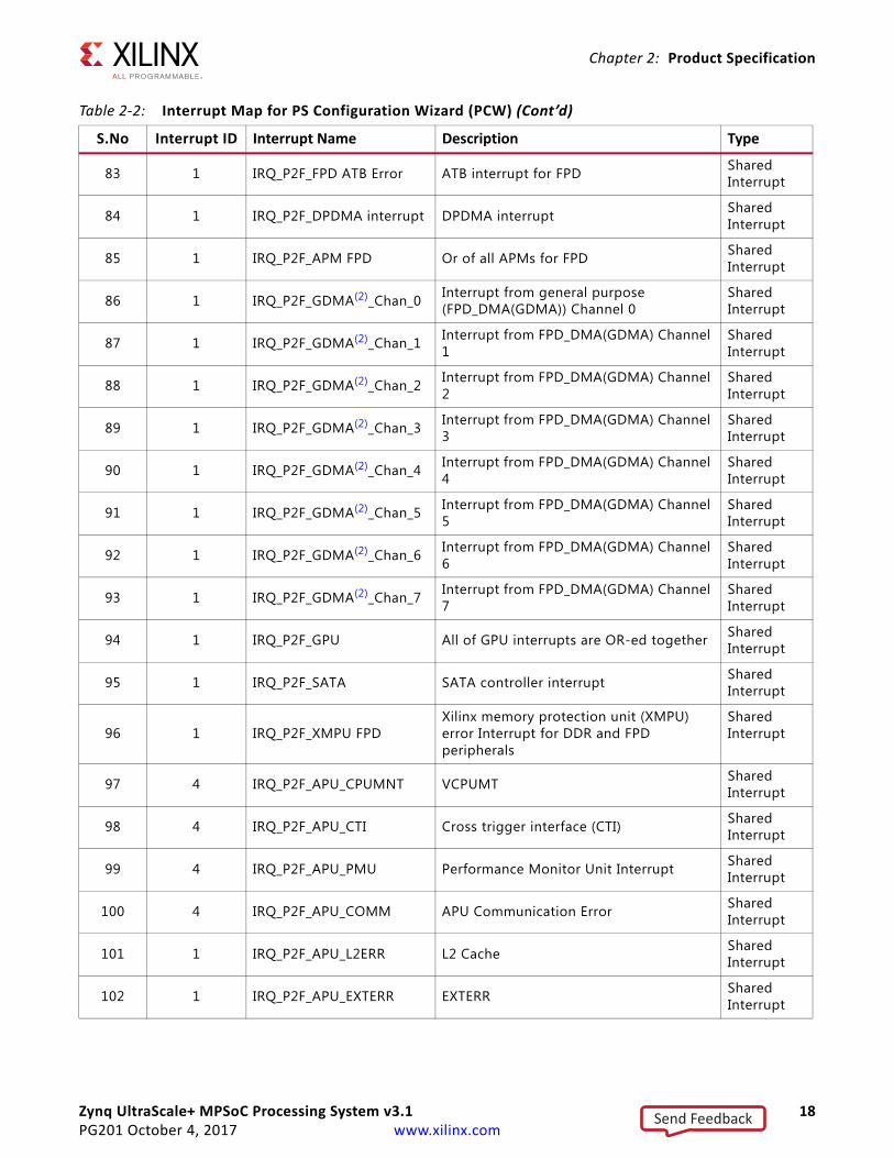
Zynq UltraScale+ MPSoC Processing System v3.1 18PG201 October 4, 2017 www.xilinx.com
Chapter 2: Product Specification
83 1 IRQ_P2F_FPD ATB Error ATB interrupt for FPD Shared Interrupt
84 1 IRQ_P2F_DPDMA interrupt DPDMA interrupt Shared Interrupt
85 1 IRQ_P2F_APM FPD Or of all APMs for FPD Shared Interrupt
86 1 IRQ_P2F_GDMA(2)_Chan_0 Interrupt from general purpose (FPD_DMA(GDMA)) Channel 0
Shared Interrupt
87 1 IRQ_P2F_GDMA(2)_Chan_1 Interrupt from FPD_DMA(GDMA) Channel 1
Shared Interrupt
88 1 IRQ_P2F_GDMA(2)_Chan_2 Interrupt from FPD_DMA(GDMA) Channel 2
Shared Interrupt
89 1 IRQ_P2F_GDMA(2)_Chan_3 Interrupt from FPD_DMA(GDMA) Channel 3
Shared Interrupt
90 1 IRQ_P2F_GDMA(2)_Chan_4 Interrupt from FPD_DMA(GDMA) Channel 4
Shared Interrupt
91 1 IRQ_P2F_GDMA(2)_Chan_5 Interrupt from FPD_DMA(GDMA) Channel 5
Shared Interrupt
92 1 IRQ_P2F_GDMA(2)_Chan_6 Interrupt from FPD_DMA(GDMA) Channel 6
Shared Interrupt
93 1 IRQ_P2F_GDMA(2)_Chan_7 Interrupt from FPD_DMA(GDMA) Channel 7
Shared Interrupt
94 1 IRQ_P2F_GPU All of GPU interrupts are OR-ed together Shared Interrupt
95 1 IRQ_P2F_SATA SATA controller interrupt Shared Interrupt
96 1 IRQ_P2F_XMPU FPDXilinx memory protection unit (XMPU) error Interrupt for DDR and FPD peripherals
Shared Interrupt
97 4 IRQ_P2F_APU_CPUMNT VCPUMT Shared Interrupt
98 4 IRQ_P2F_APU_CTI Cross trigger interface (CTI) Shared Interrupt
99 4 IRQ_P2F_APU_PMU Performance Monitor Unit Interrupt Shared Interrupt
100 4 IRQ_P2F_APU_COMM APU Communication Error Shared Interrupt
101 1 IRQ_P2F_APU_L2ERR L2 Cache Shared Interrupt
102 1 IRQ_P2F_APU_EXTERR EXTERR Shared Interrupt
Table 2‐2: Interrupt Map for PS Configuration Wizard (PCW) (Cont’d)
S.No Interrupt ID Interrupt Name Description Type
Send Feedback
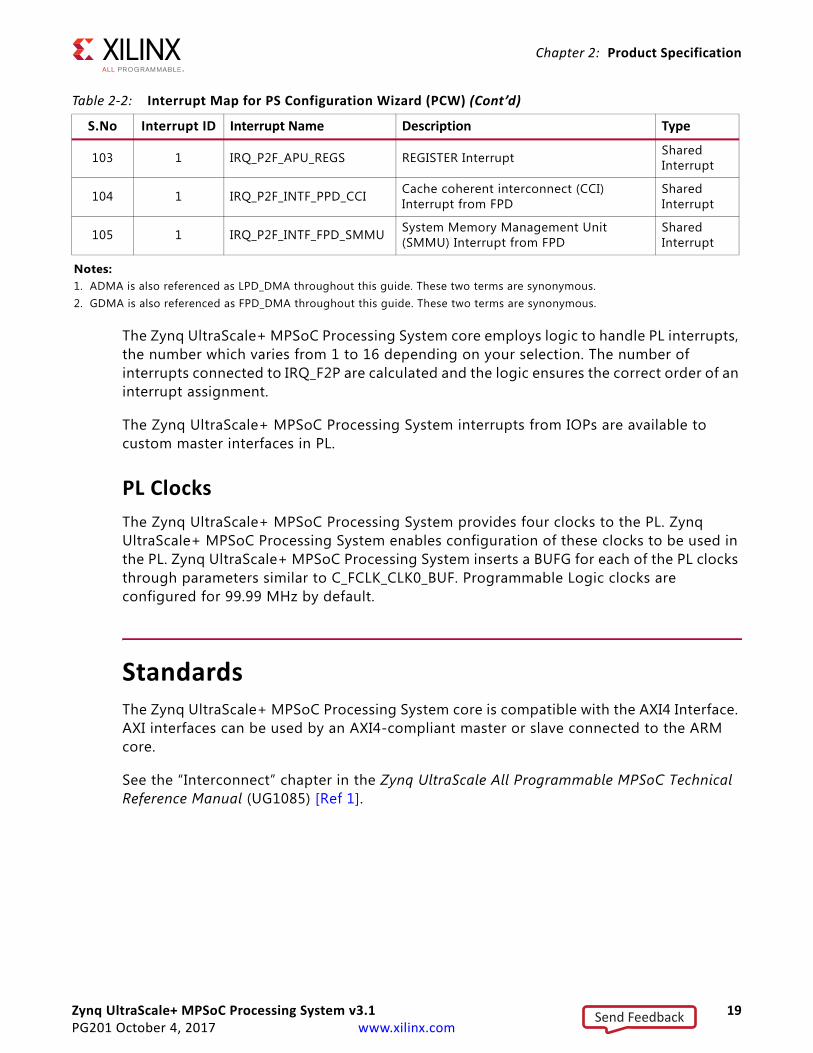
Zynq UltraScale+ MPSoC Processing System v3.1 19PG201 October 4, 2017 www.xilinx.com
Chapter 2: Product Specification
The Zynq UltraScale+ MPSoC Processing System core employs logic to handle PL interrupts, the number which varies from 1 to 16 depending on your selection. The number of interrupts connected to IRQ_F2P are calculated and the logic ensures the correct order of an interrupt assignment.
The Zynq UltraScale+ MPSoC Processing System interrupts from IOPs are available to custom master interfaces in PL.
PL Clocks
The Zynq UltraScale+ MPSoC Processing System provides four clocks to the PL. Zynq UltraScale+ MPSoC Processing System enables configuration of these clocks to be used in the PL. Zynq UltraScale+ MPSoC Processing System inserts a BUFG for each of the PL clocks through parameters similar to C_FCLK_CLK0_BUF. Programmable Logic clocks are configured for 99.99 MHz by default.
StandardsThe Zynq UltraScale+ MPSoC Processing System core is compatible with the AXI4 Interface. AXI interfaces can be used by an AXI4-compliant master or slave connected to the ARM core.
See the “Interconnect” chapter in the Zynq UltraScale All Programmable MPSoC Technical Reference Manual (UG1085) [Ref 1].
103 1 IRQ_P2F_APU_REGS REGISTER Interrupt Shared Interrupt
104 1 IRQ_P2F_INTF_PPD_CCI Cache coherent interconnect (CCI) Interrupt from FPD
Shared Interrupt
105 1 IRQ_P2F_INTF_FPD_SMMU System Memory Management Unit (SMMU) Interrupt from FPD
Shared Interrupt
Notes: 1. ADMA is also referenced as LPD_DMA throughout this guide. These two terms are synonymous.2. GDMA is also referenced as FPD_DMA throughout this guide. These two terms are synonymous.
Table 2‐2: Interrupt Map for PS Configuration Wizard (PCW) (Cont’d)
S.No Interrupt ID Interrupt Name Description Type
Send Feedback

Zynq UltraScale+ MPSoC Processing System v3.1 20PG201 October 4, 2017 www.xilinx.com
Chapter 2: Product Specification
PerformanceFor information, see the “PL and Memory System Performance Overview” section in the “Programmable Logic Design Guide” chapter of the Zynq UltraScale All Programmable MPSoC Technical Reference Manual (UG1085) [Ref 1].
Maximum Frequencies
For information, see the Zynq UltraScale All Programmable MPSoC Technical Reference Manual (UG1085) [Ref 1]
Latency
For information, see the Zynq UltraScale All Programmable MPSoC Technical Reference Manual (UG1085) [Ref 1]
Throughput
For information, see the Zynq UltraScale All Programmable MPSoC Technical Reference Manual (UG1085) [Ref 1]
Power
For information, see the Zynq UltraScale All Programmable MPSoC Technical Reference Manual (UG1085) [Ref 1]
Resource UtilizationZynq UltraScale+ MPSoC is a hard IP core so this section does not apply to this core.
Port DescriptionsSee Appendix B, Port Descriptions for all of the tables.
Send Feedback

Zynq UltraScale+ MPSoC Processing System v3.1 21PG201 October 4, 2017 www.xilinx.com
Chapter 2: Product Specification
Register SpaceNote: For register information, see the Zynq UltraScale+ MPSoC Register Reference User Guide (UG1087) [Ref 2].
The Zynq UltraScale+ MPSoC Processing System core provides access from PL masters to PS internal peripherals, and memory through AXI FIFO interface (AFI) interfaces. The Vivado IP integrator address editor provides various address segments with a fixed address for each slave interface. The availability of the address segments is controlled through the following addressing parameters.
• Detailed IOP address space: Provides individual address spaces for PS internal peripherals.
• Allow access to PS/SLCR registers: Allows address mapping to PS and system level control registers (SLCR) register space.
• Detailed PS/SLCR address space: Provides individual address spaces for PS/SLCR registers.
The PS address space accessible from the PL consists of DDR, OCM, static memory controller (SMC) memories, SLCR registers, PS I/O peripheral registers, and PS system registers. For more information, see the “System Addresses” chapter of the Zynq UltraScale All Programmable MPSoC Technical Reference Manual (UG1085) [Ref 1].
Send Feedback

Zynq UltraScale+ MPSoC Processing System v3.1 22PG201 October 4, 2017 www.xilinx.com
Chapter 3
Designing with the CoreThis chapter includes guidelines and additional information to facilitate designing with the core.
General Design GuidelinesThere are three interfaces through which the Zynq® UltraScale+™ Processing System core can access the PL side peripherals and vice versa. For more details, see the individual sections of AXI_HP and AXI_ACP interfaces in the “Interconnect” chapter of the Zynq UltraScale All Programmable MPSoC Technical Reference Manual (UG1085) [Ref 1].
InterruptsTo connect multiple interrupts in IP integrator, use a concat block to merge the individual signals together before connecting to the core. The interrupt port will be automatically expanded to match the resulting output with the concat block.
ClockingThere are four clock groups.
• Main Clock Group (MCG). This group has five PLLs.
° I/O PLL
° RPU PLL
° APU PLL
° DDR PLL
° Video PLL
Send Feedback

Zynq UltraScale+ MPSoC Processing System v3.1 23PG201 October 4, 2017 www.xilinx.com
Chapter 3: Designing with the Core
• Secure Clock Group (SCG). This group has two PLLs.
° eFuse
° PMU
• RTC Clock Group (RCG). This is Real Time Clock, a dedicated internal clock for RTC. The RTC clock group (RCG) provides a 32 KHZ clock to the RTC in the battery power domain (BPU). It is an extremely small clock domain compared with the other two clock groups. There is no clock divider required for this clock.
• Interface Clock Group (ICG). This group has clocks that are provided externally, like clocks from physical-side interface (PHY) and PL.
PL side peripherals can be operated through a PL clock (FCLK_CLK0…3). They generate the frequency ranges from 0.1 to 250 MHz.
ResetsThere are many applicable resets:
• External power on reset (POR) - Triggered by external pin assertion
• Internal POR - Triggered by software register write or safety errors.
• "System" reset - Triggered by external pin assertion, or register write or safety errors. This reset does not reset debug logic.
• PS "System" reset - Triggered by a hardware error or by a register write. This is a PS only reset and PL remains active.
• PS POR reset - Similar to External POR but only for PS
• Full power subsystem (FPS) reset - Triggered by error or register write and used to reset Full Power Domain
• RPU Reset - Triggered by errors or register write, explicitly to reset RPU
See Fabric Reset Enable in Chapter 4. Also for more details about the individual resets, see the Zynq UltraScale All Programmable MPSoC Technical Reference Manual (UG1085) [Ref 1].
Send Feedback
Zynq UltraScale+ MPSoC Processing System v3.1 24PG201 October 4, 2017 www.xilinx.com
Chapter 4
Design Flow StepsThis chapter describes customizing and generating the core, constraining the core, and the simulation, synthesis and implementation steps that are specific to this IP core. More detailed information about the standard Vivado® design flows and the IP integrator can be found in the following Vivado Design Suite user guides:
• Vivado Design Suite User Guide: Designing IP Subsystems using IP Integrator (UG994) [Ref 3]
• Vivado Design Suite User Guide: Designing with IP (UG896) [Ref 4]
• Vivado Design Suite User Guide: Getting Started (UG910) [Ref 5]
• Vivado Design Suite User Guide: Logic Simulation (UG900) [Ref 6]
Customizing and Generating the CoreThis section includes information about using the Vivado Design Suite to customize and generate the core.
If you are customizing and generating the core in the Vivado IP integrator, see the Vivado Design Suite User Guide: Designing IP Subsystems using IP Integrator (UG994) [Ref 3] for detailed information. The IP integrator might auto-compute certain configuration values when validating or generating the design, as noted in this section. To check whether the values do change, see the description of the parameters in this chapter. To view the parameter value, run the validate_bd_design command in the Tcl Console.
You can customize the IP for use in your design by specifying values for the various parameters associated with the IP core in the IP integrator using the following steps:
1. Select the IP from the Vivado IP catalog.
2. Double-click the selected IP, or select the Customize IP command from the toolbar or right-click menu.
For details, see the Vivado Design Suite User Guide: Designing with IP (UG896) [Ref 4], and the Vivado Design Suite User Guide: Getting Started (UG910). [Ref 5].
Send Feedback
Zynq UltraScale+ MPSoC Processing System v3.1 25PG201 October 4, 2017 www.xilinx.com
Chapter 4: Design Flow Steps
The Zynq UltraScale+ Block Design page with a block diagram appears in the window (Figure 4-4). Review the contents of the block diagram. The green colored blocks in the diagram are configurable.
TIP: To open the corresponding configuration page, you can click a green block, or select the page in the Page Navigator at the left side.
Note: Figures in this chapter are illustrations of the Vivado Integrated Design Environment (IDE). This layout might vary from the current version.
Preset Support
This section discusses two presets: IP preset and board preset.
IP Preset
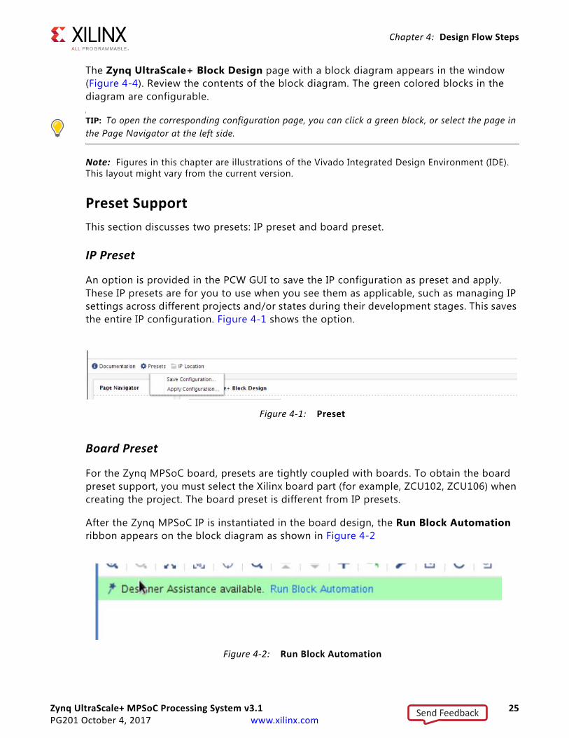
An option is provided in the PCW GUI to save the IP configuration as preset and apply. These IP presets are for you to use when you see them as applicable, such as managing IP settings across different projects and/or states during their development stages. This saves the entire IP configuration. Figure 4-1 shows the option.
Board Preset
For the Zynq MPSoC board, presets are tightly coupled with boards. To obtain the board preset support, you must select the Xilinx board part (for example, ZCU102, ZCU106) when creating the project. The board preset is different from IP presets.
After the Zynq MPSoC IP is instantiated in the board design, the Run Block Automation ribbon appears on the block diagram as shown in Figure 4-2
X-Ref Target - Figure 4-1
Figure 4‐1: Preset
X-Ref Target - Figure 4-2
Figure 4‐2: Run Block Automation
Send Feedback

Zynq UltraScale+ MPSoC Processing System v3.1 26PG201 October 4, 2017 www.xilinx.com
Chapter 4: Design Flow Steps
After clicking Run Block Automation, Apply Board Preset appears as shown in Figure 4-3.
You can re-customize your needs after preset is applied, but for the devices earlier than production (es-1, es-2) the Run Block Automation ribbon appears again on the block diagram upon re customization, but you can safely ignore this.
X-Ref Target - Figure 4-3
Figure 4‐3: Apply Board Reset
Send Feedback

Zynq UltraScale+ MPSoC Processing System v3.1 27PG201 October 4, 2017 www.xilinx.com
Chapter 4: Design Flow Steps
PS Zynq UltraScale+ MPSoC Block Design
The colors in the PS UltraScale+™ Block Design page have the following meanings:
• Light Green color shows Low Power Domain
• Light Orange color shows Full Power Domain
• Dark Green color shows the components that you can configure.
X-Ref Target - Figure 4-4
Figure 4‐4: PS Zynq UltraScale+ Block Design Page
Send Feedback

Zynq UltraScale+ MPSoC Processing System v3.1 28PG201 October 4, 2017 www.xilinx.com
Chapter 4: Design Flow Steps
I/O ConfigurationThis page shows pin assignments for individual signals of an interface of PS components. You can assign attributes for the signals.
MIO Voltage Standard
Each of these I/O pins can be routed through MIOs, EMIOs, or GT Lanes as applicable. Each peripheral pin can be routed through a subset of 78 MIOs as required. Alternatively the same pins from each peripheral can be routed to EMIO signals which brings the signal to PL section of the device for further processing.
For more information on the MIO and EMIO, refer to the Multiplexed I/O, chapter 26 in the Zynq UltraScale All Programmable MPSoC Technical Reference Manual (UG1085) [Ref 1].
MIOs available for peripheral pinouts are divided into three Banks: Bank0 (MIO 0-25), Bank1 (MIO 26-51), and Bank2 (MIO 52-77). Each bank has a common I/O Voltage Standard for all its MIOs and the default value for this is LVCMOS33.
X-Ref Target - Figure 4-5
Figure 4‐5: I/O Configuration Page
Send Feedback
Zynq UltraScale+ MPSoC Processing System v3.1 29PG201 October 4, 2017 www.xilinx.com
Chapter 4: Design Flow Steps
Peripheral
Low Speed
• Memory Interface. These are the static memory controllers present in the PS.
• I/O Peripherals. These are the I/O peripherals present in the PS.
• Application Processing Unit. These are APU specific resources such as watch dog timer, Trace and Triple Timer Counter.
High Speed
Pins from high-speed peripherals, like, PCIe, SATA, Gigabit Ethernet Module (GEM) (in SGMII mode), Display Port and USB 3.0 can be routed to SERDES by selecting the appropriate GT lanes in the I/O column.
I/O Configuration Columns
• I/O – Used to configure I/O pins of the respective peripherals.
• Signal – Displays information about the signal name driven by the respective I/O pins.
• I/O Type – CMOS/Schmitt. Select CMOS or Schmitt as the input I/O voltage type. The Schmitt Voltage type has a higher tolerance to noise than CMOS voltage type.
• Drive Strength (mA) – Used to select the drive strength. Possible values are 2, 4, 8, and 12.
• Speed – Fast/Slow. Specifies whether the device is fast or slow depending on the slew rate. If the slew rate is 0, the device is fast; else the device is slow.
• Pull Type – Used to enable/disable a device along with pull up or pull down. Possible values are pullup, pulldown, and disable.
• Direction – The direction can be fixed for certain signals.
Send Feedback
Zynq UltraScale+ MPSoC Processing System v3.1 30PG201 October 4, 2017 www.xilinx.com
Chapter 4: Design Flow Steps
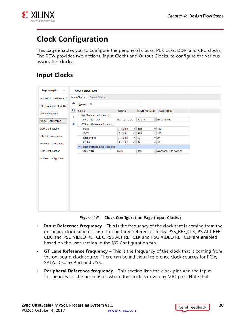
Clock ConfigurationThis page enables you to configure the peripheral clocks, PL clocks, DDR, and CPU clocks. The PCW provides two options, Input Clocks and Output Clocks, to configure the various associated clocks.
Input Clocks
• Input Reference frequency – This is the frequency of the clock that is coming from the on-board clock source. There can be three reference clocks: PSS_REF_CLK, PS ALT REF CLK, and PSU VIDEO REF CLK. PSS ALT REF CLK and PSU VIDEO REF CLK are enabled based on the user section in the I/O Configuration tab.
• GT Lane Reference frequency – This is the frequency of the clock that is coming from the on-board clock source. There can be individual reference clock sources for PCIe, SATA, Display Port and USB.
• Peripheral Reference frequency – This section lists the clock pins and the input frequencies for the peripherals where the clock is driven by MIO pins. Note that
X-Ref Target - Figure 4-6
Figure 4‐6: Clock Configuration Page (Input Clocks)
Send Feedback
Zynq UltraScale+ MPSoC Processing System v3.1 31PG201 October 4, 2017 www.xilinx.com
Chapter 4: Design Flow Steps
MIOCLK for the corresponding peripherals needs to be enabled in the I/O Configuration page for the pin to be listed here.
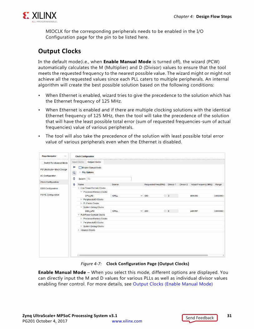
Output Clocks
In the default mode(i.e., when Enable Manual Mode is turned off), the wizard (PCW) automatically calculates the M (Multiplier) and D (Divisor) values to ensure that the tool meets the requested frequency to the nearest possible value. The wizard might or might not achieve all the requested values since each PLL caters to multiple peripherals. An internal algorithm will create the best possible solution based on the following conditions:
• When Ethernet is enabled, wizard tries to give the precedence to the solution which has the Ethernet frequency of 125 MHz.
• When Ethernet is enabled and if there are multiple clocking solutions with the identical Ethernet frequency of 125 MHz, then the tool will take the precedence of the solution that will have the least possible total error (sum of requested frequencies-sum of actual frequencies) value of various peripherals.
• The tool will also take the precedence of the solution with least possible total error value of various peripherals even when the Ethernet is disabled.
Enable Manual Mode – When you select this mode, different options are displayed. You can directly input the M and D values for various PLLs as well as individual divisor values enabling finer control. For more details, see Output Clocks (Enable Manual Mode)
X-Ref Target - Figure 4-7
Figure 4‐7: Clock Configuration Page (Output Clocks)
Send Feedback
Zynq UltraScale+ MPSoC Processing System v3.1 32PG201 October 4, 2017 www.xilinx.com
Chapter 4: Design Flow Steps
Low Power Domain Clocks
• Processor/Memory Clocks – Clock configuration for the CPU_R5 Processor
• Peripherals/IO Clocks – Clock configuration for low-speed peripheral devices.
• PL Clocks – PS generated clock to PL: PL0, PL1, PL2, and PL3
• System Debug Clocks – Clock configuration for debug modules DBG_LPD
Full Power Domain Clocks
• Processor/Memory Clocks – Clock configuration for A53 CPU (ACPU), GPU, and DDR
• Peripherals/IO Clocks – Clock configuration for low-speed peripheral devices.
• System Debug Clocks – Clock configuration for debug modules: DBG_FPD,DBG_TRACE, and DBG_TSTMP
Advance Clocks
• Low Power Domain Interconnect and Switch clocks – Clocks used by the interconnect and switches internal to the PS.
• Full Power Domain Interconnect and Switch clocks – Clocks used by the interconnect and switches internal to the PS.
Column Descriptions for Output Clocks
• Source – This is the source PLL for the corresponding peripheral.
• Requested Freq (MHz) – This is the input frequency given to the corresponding peripheral
• Divisor 1 – Denotes the 1st stage 6-bit programmable Divisor
• Divisor 2 – Denotes the 2nd stage 6-bit programmable Divisor
• Actual Freq (MHz) – This is the actual frequency calculated by the Processor Configuration Wizard. The clocking algorithm works with multiple factors, peripherals, PLLs and priorities; therefore, in certain cases, the actual frequency might be different than the Input Frequency.
• Range (MHz) – This is the Minimum/Maximum range of the frequency that the corresponding peripheral can work with. In this mode, you must configure the M and D values to achieve the desired frequency. When this mode is enabled, the values requested through Output mode will be overwritten
Note: In order to modify the clock frequencies/divisors, the corresponding clock must be enabled
Send Feedback
Zynq UltraScale+ MPSoC Processing System v3.1 33PG201 October 4, 2017 www.xilinx.com
Chapter 4: Design Flow Steps
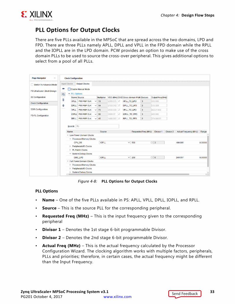
PLL Options for Output Clocks
There are five PLLs available in the MPSoC that are spread across the two domains, LPD and FPD. There are three PLLs namely APLL, DPLL and VPLL in the FPD domain while the RPLL and the IOPLL are in the LPD domain. PCW provides an option to make use of the cross domain PLLs to be used to source the cross-over peripheral. This gives additional options to select from a pool of all PLLs.
PLL Options
• Name – One of the five PLLs available in PS: APLL, VPLL, DPLL, IOPLL, and RPLL.
• Source – This is the source PLL for the corresponding peripheral.
• Requested Freq (MHz) – This is the input frequency given to the corresponding peripheral
• Divisor 1 – Denotes the 1st stage 6-bit programmable Divisor.
• Divisor 2 – Denotes the 2nd stage 6-bit programmable Divisor.
• Actual Freq (MHz) – This is the actual frequency calculated by the Processor Configuration Wizard. The clocking algorithm works with multiple factors, peripherals, PLLs and priorities; therefore, in certain cases, the actual frequency might be different than the Input Frequency.
X-Ref Target - Figure 4-8
Figure 4‐8: PLL Options for Output Clocks
Send Feedback

Zynq UltraScale+ MPSoC Processing System v3.1 34PG201 October 4, 2017 www.xilinx.com
Chapter 4: Design Flow Steps
• Range (MHz) – This is the Minimum/Maximum range of the frequency that the corresponding peripheral can work with.
Note: In the default mode, we cannot always get the actual frequency. It depends on the load on PLL (Number of different clocks in PLL drives).
Output Clocks (Enable Manual Mode)
Low Power Domain Clocks
• Processor/Memory Clocks – Clock configuration for the CPU_R5 Processor
• Peripherals/IO Clocks – Clock configuration for low-speed peripheral devices.
• PL Clocks – PS generated clock to PL: PL0, PL1, PL2, and PL3
• System Debug Clocks – Clock configuration for debug modules DBG_LPD
Full Power Domain Clocks
• Processor/Memory Clocks – Clock configuration for A53 CPU (ACPU), GPU, and DDR
• Peripherals/IO Clocks – Clock configuration for low-speed peripheral devices.
• System Debug Clocks – Clock configuration for debug modules: DBG_FPD,DBG_TRACE, and DBG_TSTMP
X-Ref Target - Figure 4-9
Figure 4‐9: Manual Mode
Send Feedback
Zynq UltraScale+ MPSoC Processing System v3.1 35PG201 October 4, 2017 www.xilinx.com
Chapter 4: Design Flow Steps
Clock Configuration Columns for Output Clocks
• Source – This is the source PLL for the corresponding peripheral.
• Requested Freq (MHz) – This is the input frequency given to the corresponding peripheral. The values in this column are not applicable in the manual mode and should be ignored. These are used only in automatic mode.
• Divisor 1 – Denotes the 1st stage 6-bit programmable Divisor.
• Divisor 2 – Denotes the 2nd stage 6-bit programmable Divisor.
• Actual Freq (MHz) – In Manual Mode, the actual frequency is a result of your selection of PLL Multiplier (M) and Divide (D) choices.
• Range (MHz) – This is the Minimum/Maximum range of the frequency that the corresponding peripheral can work with.
Send Feedback

Zynq UltraScale+ MPSoC Processing System v3.1 36PG201 October 4, 2017 www.xilinx.com
Chapter 4: Design Flow Steps
Fractional ClockingThe fractional clocking enable (FracEn) option is provided in Vivado IDE only for the DP_VIDEO and DP_AUDIO peripherals to facilitate the precise clocking as these require very precise clocking. When this option is checked/enabled the fractional value for the feedback value is configured for the respective PLL. See Figure 4-10.
X-Ref Target - Figure 4-10
Figure 4‐10: FracEnable
Send Feedback
Zynq UltraScale+ MPSoC Processing System v3.1 37PG201 October 4, 2017 www.xilinx.com
Chapter 4: Design Flow Steps
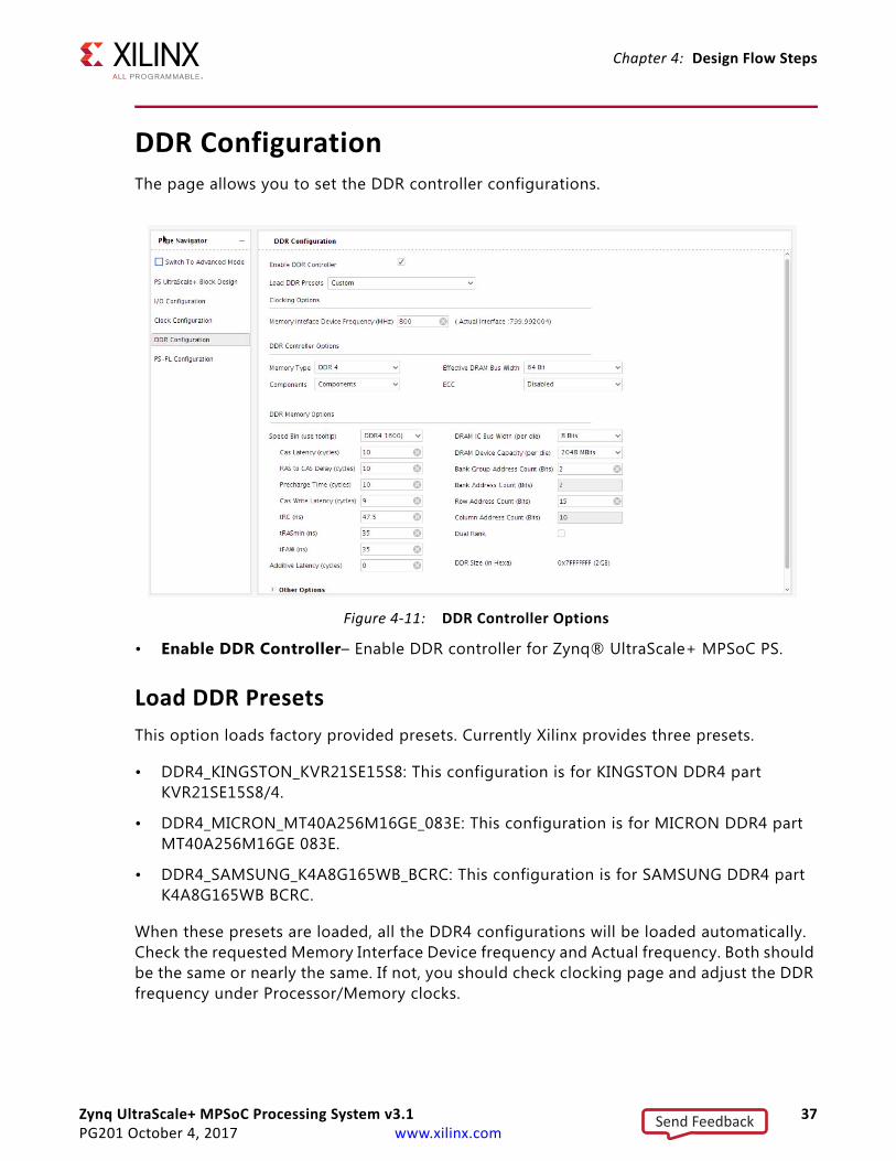
DDR ConfigurationThe page allows you to set the DDR controller configurations.
• Enable DDR Controller– Enable DDR controller for Zynq® UltraScale+ MPSoC PS.
Load DDR Presets
This option loads factory provided presets. Currently Xilinx provides three presets.
• DDR4_KINGSTON_KVR21SE15S8: This configuration is for KINGSTON DDR4 part KVR21SE15S8/4.
• DDR4_MICRON_MT40A256M16GE_083E: This configuration is for MICRON DDR4 part MT40A256M16GE 083E.
• DDR4_SAMSUNG_K4A8G165WB_BCRC: This configuration is for SAMSUNG DDR4 part K4A8G165WB BCRC.
When these presets are loaded, all the DDR4 configurations will be loaded automatically. Check the requested Memory Interface Device frequency and Actual frequency. Both should be the same or nearly the same. If not, you should check clocking page and adjust the DDR frequency under Processor/Memory clocks.
X-Ref Target - Figure 4-11
Figure 4‐11: DDR Controller Options
Send Feedback
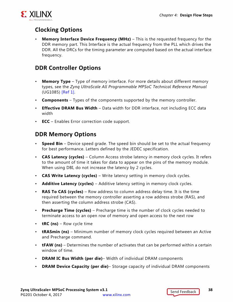
Zynq UltraScale+ MPSoC Processing System v3.1 38PG201 October 4, 2017 www.xilinx.com
Chapter 4: Design Flow Steps
Clocking Options
• Memory Interface Device Frequency (MHz) – This is the requested frequency for the DDR memory part. This Interface is the actual frequency from the PLL which drives the DDR. All the DRCs for the timing parameter are computed based on the actual interface frequency.
DDR Controller Options
• Memory Type – Type of memory interface. For more details about different memory types, see the Zynq UltraScale All Programmable MPSoC Technical Reference Manual (UG1085) [Ref 1].
• Components – Types of the components supported by the memory controller.
• Effective DRAM Bus Width – Data width for DDR interface, not including ECC data width
• ECC – Enables Error correction code support.
DDR Memory Options
• Speed Bin – Device speed grade. The speed bin should be set to the actual frequency for best performance. Letters defined by the JEDEC specification.
• CAS Latency (cycles) – Column Access strobe latency in memory clock cycles. It refers to the amount of time it takes for data to appear on the pins of the memory module. When using DBI, do not increase the latency by 2 cycles.
• CAS Write Latency (cycles) – Write latency setting in memory clock cycles.
• Additive Latency (cycles) – Additive latency setting in memory clock cycles.
• RAS To CAS (cycles) – Row address to column address delay time. It is the time required between the memory controller asserting a row address strobe (RAS), and then asserting the column address strobe (CAS).
• Precharge Time (cycles) – Precharge time is the number of clock cycles needed to terminate access to an open row of memory and open access to the next row
• tRC (ns) – Row cycle time
• tRASmin (ns) – Minimum number of memory clock cycles required between an Active and Precharge command.
• tFAW (ns) – Determines the number of activates that can be performed within a certain window of time.
• DRAM IC Bus Width (per die)– Width of individual DRAM components
• DRAM Device Capacity (per die)– Storage capacity of individual DRAM components
Send Feedback
Zynq UltraScale+ MPSoC Processing System v3.1 39PG201 October 4, 2017 www.xilinx.com
Chapter 4: Design Flow Steps
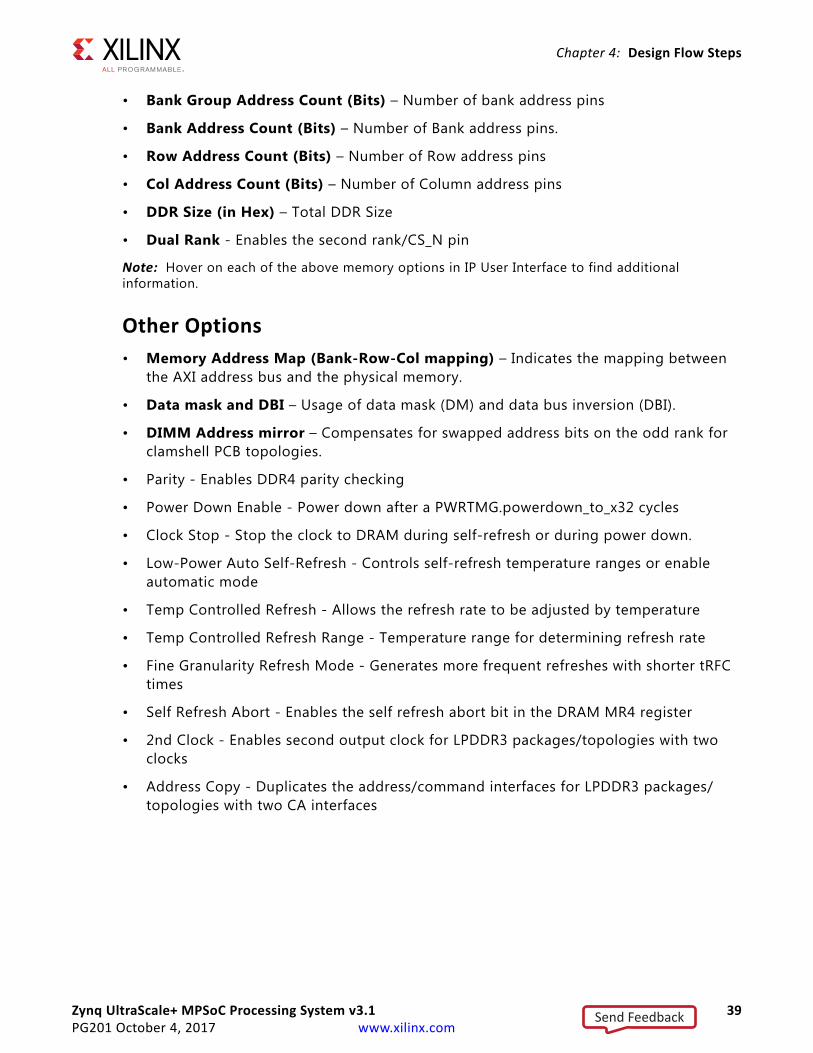
• Bank Group Address Count (Bits) – Number of bank address pins
• Bank Address Count (Bits) – Number of Bank address pins.
• Row Address Count (Bits) – Number of Row address pins
• Col Address Count (Bits) – Number of Column address pins
• DDR Size (in Hex) – Total DDR Size
• Dual Rank - Enables the second rank/CS_N pin
Note: Hover on each of the above memory options in IP User Interface to find additional information.
Other Options
• Memory Address Map (Bank-Row-Col mapping) – Indicates the mapping between the AXI address bus and the physical memory.
• Data mask and DBI – Usage of data mask (DM) and data bus inversion (DBI).
• DIMM Address mirror – Compensates for swapped address bits on the odd rank for clamshell PCB topologies.
• Parity - Enables DDR4 parity checking
• Power Down Enable - Power down after a PWRTMG.powerdown_to_x32 cycles
• Clock Stop - Stop the clock to DRAM during self-refresh or during power down.
• Low-Power Auto Self-Refresh - Controls self-refresh temperature ranges or enable automatic mode
• Temp Controlled Refresh - Allows the refresh rate to be adjusted by temperature
• Temp Controlled Refresh Range - Temperature range for determining refresh rate
• Fine Granularity Refresh Mode - Generates more frequent refreshes with shorter tRFC times
• Self Refresh Abort - Enables the self refresh abort bit in the DRAM MR4 register
• 2nd Clock - Enables second output clock for LPDDR3 packages/topologies with two clocks
• Address Copy - Duplicates the address/command interfaces for LPDDR3 packages/topologies with two CA interfaces
Send Feedback
Zynq UltraScale+ MPSoC Processing System v3.1 40PG201 October 4, 2017 www.xilinx.com
Chapter 4: Design Flow Steps
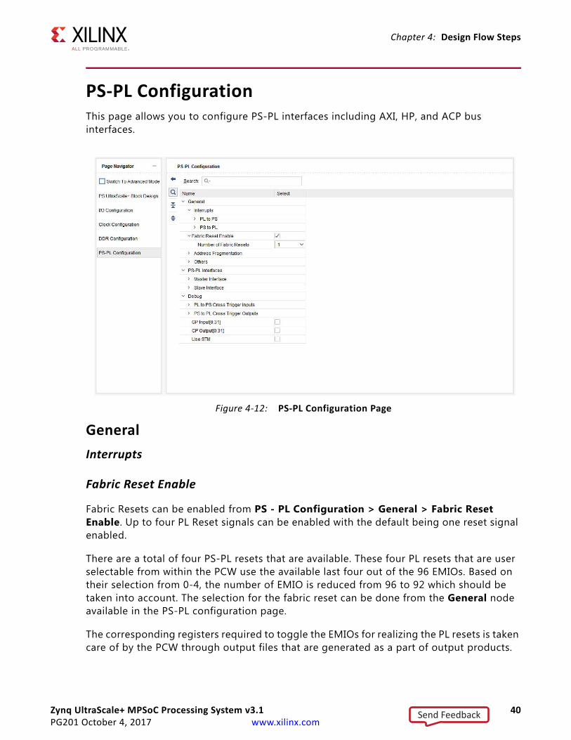
PS-PL ConfigurationThis page allows you to configure PS-PL interfaces including AXI, HP, and ACP bus interfaces.
General
Interrupts
Fabric Reset Enable
Fabric Resets can be enabled from PS - PL Configuration > General > Fabric Reset Enable. Up to four PL Reset signals can be enabled with the default being one reset signal enabled.
There are a total of four PS-PL resets that are available. These four PL resets that are user selectable from within the PCW use the available last four out of the 96 EMIOs. Based on their selection from 0-4, the number of EMIO is reduced from 96 to 92 which should be taken into account. The selection for the fabric reset can be done from the General node available in the PS-PL configuration page.
The corresponding registers required to toggle the EMIOs for realizing the PL resets is taken care of by the PCW through output files that are generated as a part of output products.
X-Ref Target - Figure 4-12
Figure 4‐12: PS-PL Configuration Page
Send Feedback

Zynq UltraScale+ MPSoC Processing System v3.1 41PG201 October 4, 2017 www.xilinx.com
Chapter 4: Design Flow Steps
Address Fragmentation
With the availability of several peripherals within PS, PCW provides an organized way to access these peripherals. The Address Fragmentation allows you to expand the peripherals based on the address space in which they are assigned within the Zynq® UltraScale+™ MPSoC. Lower LPD slaves, Upper LPD slaves, FPD slaves and others are few of the available choices. Based on the selection, only the selected segments will be shown up in the address editor in Vivado along with the addresses to which they will be mapped to the PL- master.
This way only the list of selected peripherals will appear in the address editor. This can be used where the requirement is to have more address space available for the PL components, rather than a single address block assigned to Zynq UltraScale+ MPSoC addressable components.
Notes: 1. High DDR segment is not enabled if the DDR size is less than or equal to 2GB.2. When the DDR size is greater than 2GB, the High DDR segment can be used to have DDR addressed in a higher
address space, this is limited to 4GB of DDR size.3. You must have a 64-bit master in the PL in order to access higher address space above 4GB.
For more information, see the Zynq UltraScale All Programmable MPSoC Technical Reference Manual (UG1085) [Ref 1].
Others
• Use LPD_DMA(ADMA) – DMA in Low power domain
• Use FPD_DMA(GDMA) – DMA in Full power domain
• USE RTC – Real Time clock
• Use Event RPU and Use Proc Event Bus – The processor includes logic to detect various events that can occur, for example, a cache miss. These events provide useful information about the behavior of the processor for use when debugging or profiling code. The events are made visible on an output event bus and can be counted using registers in the performance monitoring unit.
• Live Audio and Live Video – The DisplayPort controller supports live audio and video channels from the PL. These audio and video streams interface to the DisplayPort controller and provide live audio and video overlays from the PL.
Send Feedback
Zynq UltraScale+ MPSoC Processing System v3.1 42PG201 October 4, 2017 www.xilinx.com
Chapter 4: Design Flow Steps
PS-PL Interfaces
Master Interface
° AXI HPM0 FPD – High performance master 0 in full power domain
° AXI HPM1 FPD – High performance master 1 in full power domain
° AXI HPM0 LPD – High performance master 0 in low power domain.
Each interface supports 32, 64, 1nd 128 data widths.
Slave Interface
° AXI HP and sub options – There are two (AXI HPC0 FPD, AXI HPC1 FPD) high performance AXI I/O coherent master interfaces in full-power domain; four (AXI HP0 FPD, AXI HP1 FPD, AXI HP2 FPD, AXI HP3 FPD) high performance slave AXI interfaces in full-power domain; one (AXI LPD) AXI interface in low-power domain.
Each interface supports 32, 64, 1nd 128 data widths.
° S AXI ACP – There is one Accelerator Coherency Port that can be connected to a DMA engine or a non-cached coherent master.
° S AXI ACE – There is one AXI Coherency Extension slave.
Debug
The debug feature enables configuration of cross trigger signals. This provides debug capability for accessing the PS debug structure allowing integrated test and debug on both PS and PL simultaneously.
Fabric Trigger Macrocell (FTM) For Programmable Logic Test And Debug
It is based on the ARM® CoreSight® architecture. The FTM receives trace data from the PL and formats it into trace packets to be combined with the trace packets from other trace source components such as PTM and Instrumentation Trace Macrocell (ITM). With this capability, PL events can easily be traced simultaneously with PS events.
The FTM also supports cross-triggering between the PS and PL, except for the trace dumping feature. In addition, the FTM provides general-purpose debug signals between the PS and PL.
Send Feedback

Zynq UltraScale+ MPSoC Processing System v3.1 43PG201 October 4, 2017 www.xilinx.com
Chapter 4: Design Flow Steps
This block provides:
• General purpose I/Os, 32 bits to the PL and 32 bits from the PL. These are accessed through reads and writes to registers.
• Trigger signals, four pairs to the PL and four pairs from the PL. Each pair consists of a trigger signal and an acknowledge signal, and follows the ARM standard CTI handshake protocol
Options
• PL to PS Cross Trigger Inputs – Trigger signals, four pairs from the PL. Each pair consists of a trigger signal and an acknowledge signal, and follows the ARM® standard CTI handshake protocol.
• PL to PS Cross Trigger Outputs and sub options – Trigger signals, four pairs to the PL. Each pair consists of a trigger signal and an acknowledge signal, and follows the ARM standard CTI handshake protocol.
• GP Input[0:31] GP Output[0:31] – General purpose I/Os, 32 bits to the PL and 32 bits from the PL. These are accessed through reads and writes to registers.
Advanced ConfigurationX-Ref Target - Figure 4-13
Figure 4‐13: Advanced Configuration
Send Feedback

Zynq UltraScale+ MPSoC Processing System v3.1 44PG201 October 4, 2017 www.xilinx.com
Chapter 4: Design Flow Steps
CSU and Tamper Response Settings
CSU is responsible for loading the processing system (PS) first-stage boot loader (FSBL) code into the on-chip RAM (OCM) in both secure and non-secure boot modes. You can select, through the boot header, to execute the FSBL on the Cortex®-R5 or the Cortex-A53 processor. After FSBL execution starts, the CSU enters the post-configuration stage, which is responsible for system tamper response.
The CSU can be configured to have secure lock down, system reset, and system interrupt for some of the errors like PL single event upset (SEU) error, Temperature alarm, voltage alarm, etc. These options are available under CSU Tamper Response settings on the Advanced Configuration page.
Interrupts
One external tamper interrupt is mapped to CSU through MIO. There are three interrupts from CSU (PS) to PL as CSU WDT Interrupt, CSU DMA Interrupt, and CSU interrupt.
The CSU Interrupt is used to indicate that something in the CSU logic has caused an interrupt. The CSU interrupt status register holds the interrupt bits for all of the CSU logic except for the DMA. The following values can cause an interrupt in the CSU:
For more information, see the Zynq UltraScale All Programmable MPSoC Technical Reference Manual (UG1085) [Ref 1].
• AES done – Bit to notify Advanced Encryption done.
• PL INIT complete – Bit to indicate PL initialization is complete.
• AES error – Bit to indicate Advanced Encryption error.
• RSA done – Bit to Indicate RSA Encryption done.
• PL POR_B – Bit to indicate PL power on reset status.
• TMR fatal error – Bit to indicate Triple-Mode Redundant (TMR) fatal error
• SHA done – Bit to indicate Secure Hash Algorithm Encryption done.
• PL SEU error flag – Bit to indicate Single Even Upset error.
• APB SLVERR – An error bit to indicate the failure of a transfer.
• PL CFG done – Status bit to indicate PL configuration complete.
• PCAP FIFO overflow – Status bit to indicate Processor Configuration Access Port FIFO overflow.
• CSU RAM ECC error – Bit to indicate CSU RAM ECC error.
The CSU_DMA_IRQ will alert the system that the DMA has generated an interrupt. The CSU WDT Interrupt is from the CSU watch dog timer interrupt.
Send Feedback

Zynq UltraScale+ MPSoC Processing System v3.1 45PG201 October 4, 2017 www.xilinx.com
Chapter 4: Design Flow Steps
Options
For more information, see the Zynq UltraScale All Programmable MPSoC Technical Reference Manual (UG1085) [Ref 1].
• CSU Register – Setting bits in this register causes the CSU ROM to issue a system interrupt when the tamper event occurs.
• External MIO – Observation of MIOs that causes the CSU ROM to issue a system interrupt when the tamper event occurs.
• JTAG toggle detect – Bit to identify the change in the JTAG mode.
• PLU SEU error – Bit to indicate Single Even Upset error.
• Temp Alarm for LPD – Temperature alarm for Low Power/RPU domain.
• Temp Alarm for APU – Temperature alarm for APU/ Full power domain.
• Voltage Alarm for VCCPINT_FPD – Power rail removal alarm when VCCPINT_FPD is removed.
• Voltage Alarm for VCCPINT_LPD – Power rail removal alarm when VCCPINT_LPD is removed.
• Voltage Alarm for VCCPAUX – Power rail removal alarm when VCCPAUX is removed.
• Voltage Alarm for DDRPHY – Reference voltage observation signal for DDR PHY.
• Voltage Alarm for PSIO bank 0/1/2 – Reference voltage observation signal for PSIO bank 0/1/2.
• Voltage Alarm for PSIO bank 3 – Reference voltage observation signal for PSIO bank 3.
• Voltage Alarm for GT – Reference voltage observation signal for Gigabit transceivers.
IPI Master Slave Configuration
The Inter Processor Interrupt Block provides the ability for any processing unit to interrupt another processing unit by performing a register write.
There are 11 IPI channels (GEN_IPI_0 through GEN_IPI_10), out of which four channels (Channel 3, 4, 5, 6) are dedicated to PMU. The rest of the channels can be assigned to APU, RPU, and PL. With this Master assignment to each IPI channel protects corresponding channel using XPPU from unmapped masters.
Each IPI channel provides the registers to trigger the interrupts to any destination. The XPPU only allows the master that is associated with channel to access those registers. In addition to the registers, IPI channels are provided with the payload buffers.
XPPU only allows the master that is associated with buffers to access those buffers.
Send Feedback
Zynq UltraScale+ MPSoC Processing System v3.1 46PG201 October 4, 2017 www.xilinx.com
Chapter 4: Design Flow Steps
UART Baud Rate Selection
• UART0 Baud Rate – Specifies the UART baud rate for the UART0.
• UART1 Baud Rate – Specifies the UART baud rate for the UART1.
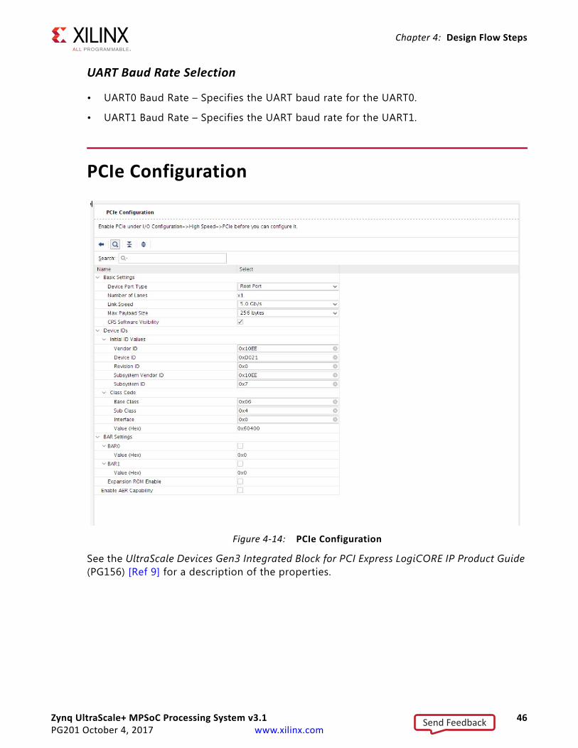
PCIe Configuration
See the UltraScale Devices Gen3 Integrated Block for PCI Express LogiCORE IP Product Guide (PG156) [Ref 9] for a description of the properties.
X-Ref Target - Figure 4-14
Figure 4‐14: PCIe Configuration
Send Feedback
Zynq UltraScale+ MPSoC Processing System v3.1 47PG201 October 4, 2017 www.xilinx.com
Chapter 4: Design Flow Steps
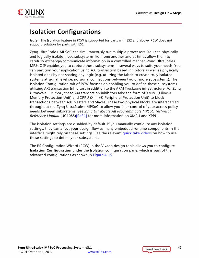
Isolation ConfigurationsNote: The Isolation feature in PCW is supported for parts with ES2 and above. PCW does not support isolation for parts with ES1.
Zynq UltraScale+ MPSoC can simultaneously run multiple processors. You can physically and logically isolate these subsystems from one another and at times allow them to carefully exchange/communicate information in a controlled manner. Zynq UltraScale+ MPSoC IP enables you to capture these subsystems in several ways to suite your needs. You can partition your application using AXI transaction based inhibitors as well as physically isolated ones by not sharing any logic (e.g. utilizing the fabric to create truly isolated systems at signal level i.e. no signal connections between two or more subsystems). The Isolation Configuration tab of PCW focuses on enabling you to define these subsystems utilizing AXI transaction Inhibitors in addition to the ARM Trustzone infrastructure. For Zynq UltraScale+ MPSoC, these AXI transaction inhibitors take the form of XMPU (Xilinx® Memory Protection Unit) and XPPU (Xilinx® Peripheral Protection Unit) to block transactions between AXI Masters and Slaves. These two physical blocks are interspersed throughout the Zynq UltraScale+ MPSoC to allow you finer control of your access policy needs between subsystems. See Zynq UltraScale All Programmable MPSoC Technical Reference Manual (UG1085)[Ref 1] for more information on XMPU and XPPU.
The isolation settings are disabled by default. If you manually configure any isolation settings, they can affect your design flow as many embedded runtime components in the interface might rely on these settings. See the relevant quick take videos on how to use these settings to define your subsystems.
The PS Configuration Wizard (PCW) in the Vivado design tools allows you to configure Isolation Configuration under the Isolation configuration pane, which is part of the advanced configurations as shown in Figure 4-15.
Send Feedback

Zynq UltraScale+ MPSoC Processing System v3.1 48PG201 October 4, 2017 www.xilinx.com
Chapter 4: Design Flow Steps
The security and protection of each peripheral or any memory is achieved by creating subsystems (a subsystem is a group of slaves: peripherals, memory regions, and masters). and adding required slaves (Peripherals, memory regions) and masters that can access the specified slaves.
PCW has a subsystem concept, where a design can be categorized as different groups (subsystems). These subsystems are conceptual in nature, and allows you to configure security settings in an easy manner.
PCW allows you to protect and isolate the memories/peripherals, which are configured in the Isolation area of the Vivado design tools. The rest of the memories and peripherals are open to all masters.
PCW provides the following
• Memory partitioning and protection (DDR with 1 MB address alignment and OCM with 4 KB address alignment).
• TrustZone settings like Non Secure and Secure.
• Access settings like Read/Write, Read-only, and Write-Only. For LPD peripherals the Write-Only option is not available
• Secure Debug
• TZ settings for masters
• Lock Unprotected Address space
X-Ref Target - Figure 4-15
Figure 4‐15: Isolation Configuration
Send Feedback
Zynq UltraScale+ MPSoC Processing System v3.1 49PG201 October 4, 2017 www.xilinx.com
Chapter 4: Design Flow Steps
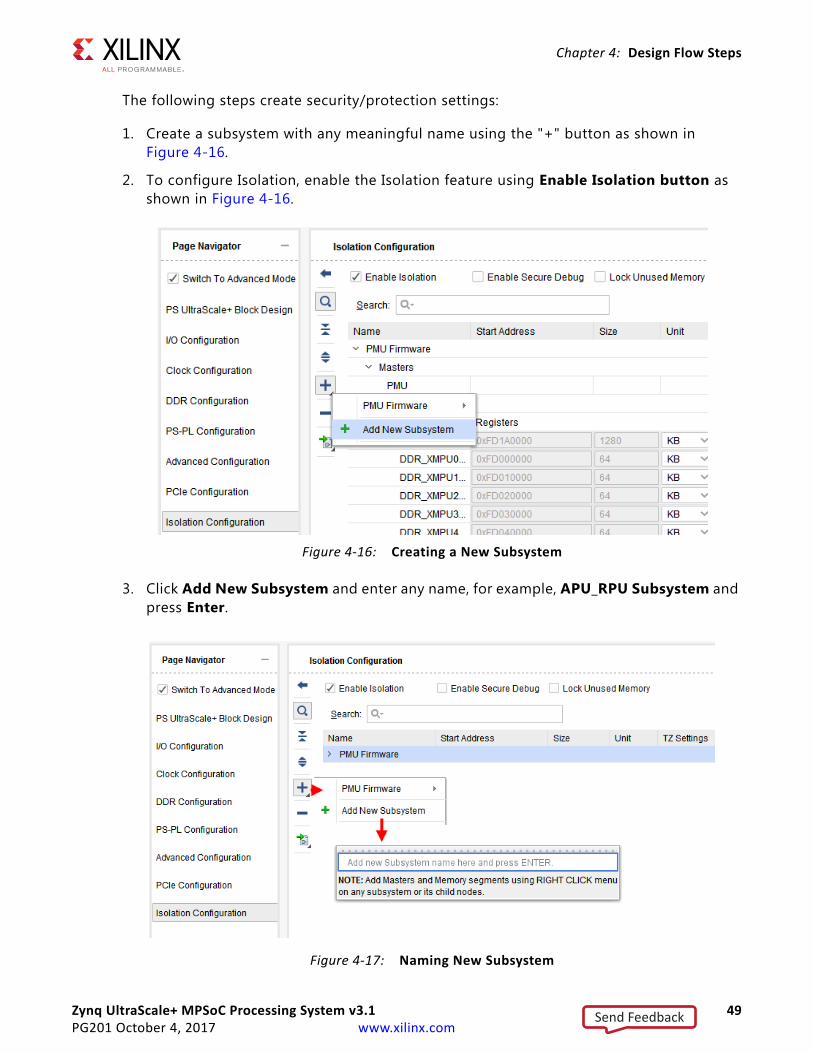
The following steps create security/protection settings:
1. Create a subsystem with any meaningful name using the "+" button as shown in Figure 4-16.
2. To configure Isolation, enable the Isolation feature using Enable Isolation button as shown in Figure 4-16.
3. Click Add New Subsystem and enter any name, for example, APU_RPU Subsystem and press Enter.
X-Ref Target - Figure 4-16
Figure 4‐16: Creating a New Subsystem
X-Ref Target - Figure 4-17
Figure 4‐17: Naming New Subsystem
Send Feedback

Zynq UltraScale+ MPSoC Processing System v3.1 50PG201 October 4, 2017 www.xilinx.com
Chapter 4: Design Flow Steps
4. Right-click APU_RPU Subsystem to add any peripheral, Memory, and Masters.
Example: Isolation settings to protect the following:
• Secure 4 MB of DDR memory from 0x00000000 with TZ as secure and Access settings as Read only to APU and RPU0
• Secure 12 KB of OCM memory from 0xFFFC0000 with TZ as secure and Access settings as Write only to APU and RPU0
• LPD peripherals UART 0, UART 1 with TZ as secure and Access settings as Read/Write only to APU and RPU0
• LPD peripherals SPI0, and SPI1 TZ as secure and Access settings as Read-Only to APU and RPU0
Perform the following steps in the PCW to create the previously described system:
1. Open the PS Configuration Wizard (PCW), go to Isolation pane under Advanced Mode
2. Click on + button and click Add new Subsystem, Enter APU subsystems and then Enter.
3. Right-click APU_RPU Subsystem and then click Add Master. Select APU,RPU0 from processors category as shown in Figure 4-18.
4. Right-click APU_RPU Subsystem and then click Add Slaves. Select DDR_LOW from Memory category.
X-Ref Target - Figure 4-18
Figure 4‐18: Adding Masters
Send Feedback

Zynq UltraScale+ MPSoC Processing System v3.1 51PG201 October 4, 2017 www.xilinx.com
Chapter 4: Design Flow Steps
5. Enter the Start Address and size of the regions, that is 0x00000000 and 4 MB.
6. Set TZ as Secure from the TZ Settings drop-down list.
7. Right-click APU_RPU Subsystem and then click Add Slaves. Select OCM from Memory category.
X-Ref Target - Figure 4-19
Figure 4‐19: Adding DDR Segment
X-Ref Target - Figure 4-20
Figure 4‐20: Setting TZ as Secure from the TZ Settings
Send Feedback
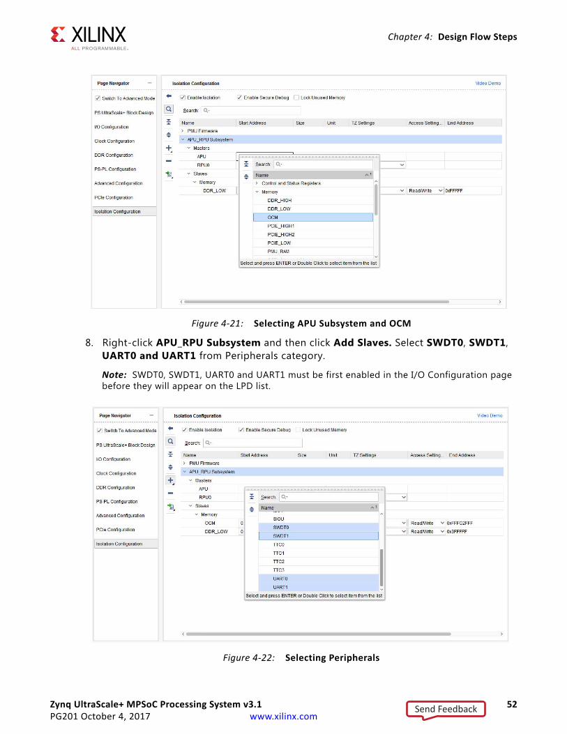
Zynq UltraScale+ MPSoC Processing System v3.1 52PG201 October 4, 2017 www.xilinx.com
Chapter 4: Design Flow Steps
8. Right-click APU_RPU Subsystem and then click Add Slaves. Select SWDT0, SWDT1, UART0 and UART1 from Peripherals category.
Note: SWDT0, SWDT1, UART0 and UART1 must be first enabled in the I/O Configuration page before they will appear on the LPD list.
X-Ref Target - Figure 4-21
Figure 4‐21: Selecting APU Subsystem and OCM
X-Ref Target - Figure 4-22
Figure 4‐22: Selecting Peripherals
Send Feedback

Zynq UltraScale+ MPSoC Processing System v3.1 53PG201 October 4, 2017 www.xilinx.com
Chapter 4: Design Flow Steps
9. For UART 0, UART 1, set TZ as Secure and Access Settings as Read/Write.
10. For SWDT0, SWDT1, set TZ as secure and Access Settings as Read-Only.
Secure Debug: By default secure debug is enabled. It means that DAP and CoreSight™ are added as masters in all the subsystems so that debugging is allowed. For the design that is this release version, this Secure Debug should be disabled.
X-Ref Target - Figure 4-23
Figure 4‐23: Access Settings as Read-Only
X-Ref Target - Figure 4-24
Figure 4‐24: Isolation Configuration -- Masters List
Send Feedback
Zynq UltraScale+ MPSoC Processing System v3.1 54PG201 October 4, 2017 www.xilinx.com
Chapter 4: Design Flow Steps
Lock Unprotected Address Space: Select this option to protect all the slaves/memory segments, control and status registers which are not mentioned or not part of any subsystems from masters. If a slave/memory segment, control and status register is not mentioned in Isolation, it cannot be accessed by any master.
PMU Firmware: By default, the PMU FW subsystem is added to Isolation configuration. You can modify/delete this subsystem as per your requirement.
You can create the PMU FW subsystem to achieve the following objectives:
1. Make PMU as a centralized processor to monitor any violations.
2. Give SLCR and control registers from all the masters and provide access to PMU only.
3. Protect XMPU and XPPU configuration registers from all other masters and provide access to PMU only.
Note: If you have your own schema to address all the above scenarios, you can have your own subsystems and can remove the PMU FW subsystem.
Known Limitations
By default, Isolation settings are partially applied by First Stage Boot Loader (FSBL). FSBL will not configure Isolation settings for Peripherals. Isolation settings for DDR and OCM XMPU only will be configured by FSBL through psu_init. To apply the Isolation settings completely, compile FSBL with FSBL_PROT_BYPASS_EXCLUDE_VAL symbol.
User ParametersThe core can be parameterized for individual applications. Parameters related to enabling interfaces or functions reflect the state of the Zynq UltraScale+ MPSoC configuration. The device configuration custom Vivado Integrated Design Environment (IDE) is available in the Vivado IP integrator and should be used to update the parameters mentioned in Table C-1.
These parameter are updated in the IP integrator. Ports related to specific peripherals are either valid or invalid. Invalid ports are not visible. The IP integrator database uses these parameters to initialize associated PS registers in the psu_init.tcl or First Stage Boot Loader (FSBL). The FSBL enables you to configure the design as needed, including the PS and PL. By default, the JTAG interface is enabled to give you access to the PS and PL for test and debug purposes.
In batch mode, the core can be configured using the set_property Tcl Console command.
Table C-1 in Appendix C, User Parameters shows the relationship between the fields in the Vivado IDE and the User Parameters (which can be viewed in the Tcl Console).
Send Feedback

Zynq UltraScale+ MPSoC Processing System v3.1 55PG201 October 4, 2017 www.xilinx.com
Chapter 4: Design Flow Steps
Output GenerationFor details about common core output files, see “Generating IP Output Products” in the Vivado Design Suite User Guide: Designing with IP (UG896) [Ref 4].
The Vivado design tool exports the Hardware Platform Specification for your design to the Software Development Kit (SDK). The following four files are exported to SDK:
• The system.hdf file opens by default when SDK launches. The address map of your system read from this file is shown by default in the SDK window.
• The psu_init.tcl, psu_init.c and psu_init.h files contain the initialization code for the Zynq UltraScale+ MPSoC processing system and initialization settings for DDR, clocks, plls, and MIOs. SDK uses these settings when initializing the processing system so that applications can be run on top of the processing system.
° psu_init.tcl: This Zynq UltraScale+ MPSoC Processor System initialization with the Tcl file is used for the device initialization Xilinx® System Debugger (XSDB) flow.
° psu_init.c: Generated by the PS Configuration Wizard (PCW), this header file for the first stage boot loader (FSBL) contains proc of a psu_init() and the return values. The FSBL uses only this file, and it calls the psu_init() functions, and checks return values.
° psu_init.h: Generated by the PCW, this file implements the psu_init(). This file also contains some testing code. This testing code enhances the testing performed by the PCW.
The supporting .c and .h files (described earlier) are also produced by the PCW.
The Zynq UltraScale MPSoC Processing System core overwrites all files when regenerated.
Constraining the CoreThis section is not applicable for this core.
Required Constraints
This section is not applicable for this core.
Device, Package, and Speed Grade Selections
This section is not applicable for this core.
Send Feedback

Zynq UltraScale+ MPSoC Processing System v3.1 56PG201 October 4, 2017 www.xilinx.com
Chapter 4: Design Flow Steps
Clock Frequencies
This section is not applicable for this core.
Clock Management
This section is not applicable for this core.
Clock Placement
This section is not applicable for this core.
Banking
This section is not applicable for this core.
Transceiver Placement
This section is not applicable for this core.
I/O Standard and Placement
This section is not applicable for this core.
SimulationAXI Verification IP for Zynq UltraScale+ MPSoC is not yet supported. This section is not applicable for this core.
Synthesis and ImplementationFor details about synthesis and implementation, see the Vivado Design Suite User Guide: Designing with IP (UG896) [Ref 4].
Send Feedback

Zynq UltraScale+ MPSoC Processing System v3.1 57PG201 October 4, 2017 www.xilinx.com
Chapter 5
Example DesignThis chapter gives an example of how to set up a DDR Configuration.
The PS Configuration Wizard (PCW), provides you with the means to configure the DDR controller for your specific DDR Memory Part in an easy and intuitive manner. The following procedure demonstrates how to build a complete DDR configuration using the PCW and taking as an example Micron's MT41K1G8SN-125:A.
1. To access the DDR configuration, select the DDR Configuration from the PCW.
Looking at the DDR Configuration page, notice that it is split into four sections, these are:
° Clocking Options
° DDR Controller Options
° DDR Memory Options
° Other OptionsX-Ref Target - Figure 5-1
Figure 5‐1: DDR Configuration
Send Feedback

Zynq UltraScale+ MPSoC Processing System v3.1 58PG201 October 4, 2017 www.xilinx.com
Chapter 5: Example Design
2. From the DDR Configuration page, create a DDR Configuration using as an example the Micron MT41K1G8SN-125:A, which denotes a DDR3 device. For this example the focus is on the DDR Controller Options and DDR Memory Options.
Note: The Micron data sheet MT41K1G8SN-125:A content in Figure 5-2 through Figure 5-6 is provided with permission of Micron Technology Inc. [Ref 8]
Note: Content of Figure 5-2 used with permission by Micron Technology, Inc. © 2010/09/04 Micron Technology, Inc., All Rights Reserved
3. Examine the first page of the data sheet in Figure 5-2 and in particular the device name. You can identify the information that is required in order to fill in the DDR Controller Options and DDR Memory Options sections of the DDR Configuration Page.
° The Device Part name provides a lot of information, for instance, 1G8 is the capacity of the device. In this case it is a 1 Gigabit Device by 8, which makes this an 8 Gigabit Device as shown as the first red rectangle Figure 5-2. There is a more in-depth calculation in the next steps.
° The Device Part name also gives information as to the speed grade of the device. In this case it is designated as -125 as in 1.25 ns which is the maximum clock period in nanoseconds in this case and a CAS latency of 11 cycles for a DDR3-1600 Speed Bin as shown as the third red rectangle in Figure 5-2. You will see a more in-depth calculation in the next steps.
° Using as an example the MT41K1G8SN-125:A device translates to the following.
- Capacity = 1 GBits x 8 = 8 GBits
X-Ref Target - Figure 5-2
Figure 5‐2: Micron Data Sheet
Send Feedback

Zynq UltraScale+ MPSoC Processing System v3.1 59PG201 October 4, 2017 www.xilinx.com
Chapter 5: Example Design
- Speed Grade = -125 1.25 ns @CL =11(DDR3-1600)1.25 ns clock cycle == operating frequency of 800 MHz
Note: Content of Figure 5-3 used with permission by Micron Technology, Inc. © 2010/09/04 Micron Technology, Inc., All Rights Reserved
° The Micron data sheet in Figure 5-3 shows an example part number and how to identify specific information of interest. For MT41K1G8SN-125:A:
- Configuration is Row 2 (1 Gig x 8, 1G8)
- Speed Grade is Row 3 (-125, tCLK =1.25ns, CL = 11)
- Temperature is Row 2 (Industrial temperature, IT)
X-Ref Target - Figure 5-3
Figure 5‐3: DDR Example Part Number
Send Feedback
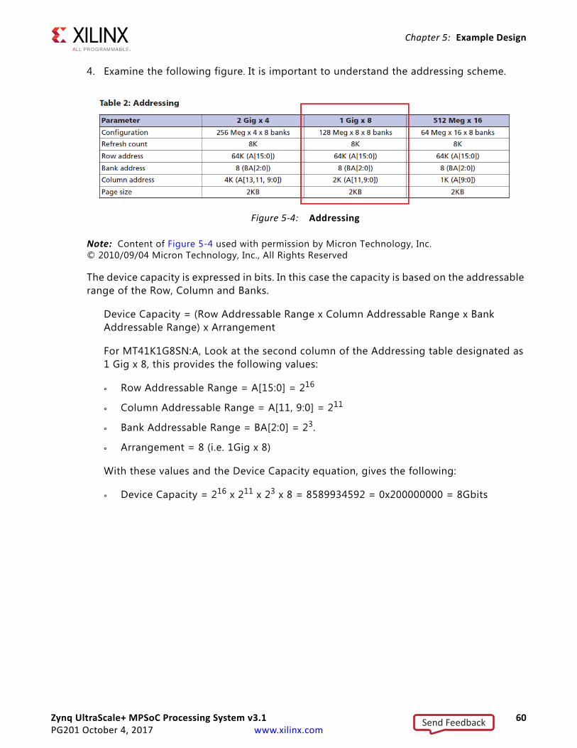
Zynq UltraScale+ MPSoC Processing System v3.1 60PG201 October 4, 2017 www.xilinx.com
Chapter 5: Example Design
4. Examine the following figure. It is important to understand the addressing scheme.
Note: Content of Figure 5-4 used with permission by Micron Technology, Inc. © 2010/09/04 Micron Technology, Inc., All Rights Reserved
The device capacity is expressed in bits. In this case the capacity is based on the addressable range of the Row, Column and Banks.
Device Capacity = (Row Addressable Range x Column Addressable Range x Bank Addressable Range) x Arrangement
For MT41K1G8SN:A, Look at the second column of the Addressing table designated as 1 Gig x 8, this provides the following values:
° Row Addressable Range = A[15:0] = 216
° Column Addressable Range = A[11, 9:0] = 211
° Bank Addressable Range = BA[2:0] = 23.
° Arrangement = 8 (i.e. 1Gig x 8)
With these values and the Device Capacity equation, gives the following:
° Device Capacity = 216 x 211 x 23 x 8 = 8589934592 = 0x200000000 = 8Gbits
X-Ref Target - Figure 5-4
Figure 5‐4: Addressing
Send Feedback

Zynq UltraScale+ MPSoC Processing System v3.1 61PG201 October 4, 2017 www.xilinx.com
Chapter 5: Example Design
5. Examine the Speed Bin and Operating Conditions in Figure 5-5.
Note: Content of Figure 5-5 used with permission by Micron Technology, Inc. © 2010/09/04 Micron Technology, Inc., All Rights Reserved
X-Ref Target - Figure 5-5
Figure 5‐5: DDR3L-1600 Speed Bins
Send Feedback
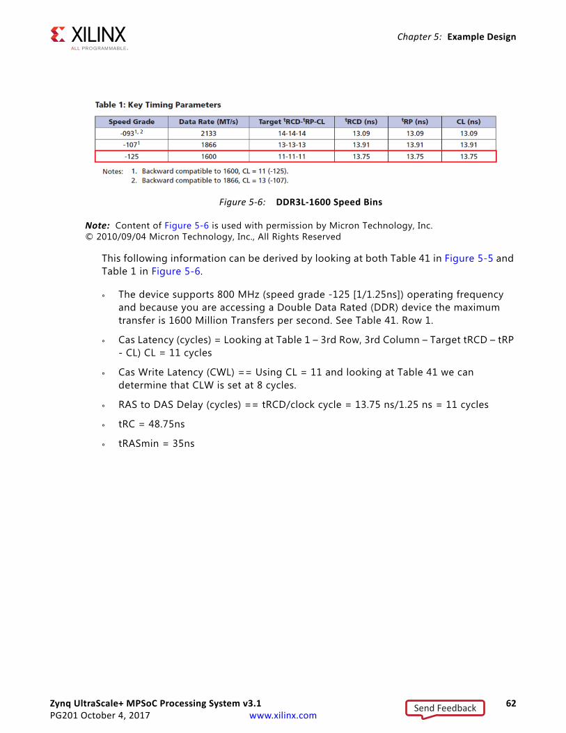
Zynq UltraScale+ MPSoC Processing System v3.1 62PG201 October 4, 2017 www.xilinx.com
Chapter 5: Example Design
Note: Content of Figure 5-6 is used with permission by Micron Technology, Inc. © 2010/09/04 Micron Technology, Inc., All Rights Reserved
This following information can be derived by looking at both Table 41 in Figure 5-5 and Table 1 in Figure 5-6.
° The device supports 800 MHz (speed grade -125 [1/1.25ns]) operating frequency and because you are accessing a Double Data Rated (DDR) device the maximum transfer is 1600 Million Transfers per second. See Table 41. Row 1.
° Cas Latency (cycles) = Looking at Table 1 – 3rd Row, 3rd Column – Target tRCD – tRP - CL) CL = 11 cycles
° Cas Write Latency (CWL) == Using CL = 11 and looking at Table 41 we can determine that CLW is set at 8 cycles.
° RAS to DAS Delay (cycles) == tRCD/clock cycle = 13.75 ns/1.25 ns = 11 cycles
° tRC = 48.75ns
° tRASmin = 35ns
X-Ref Target - Figure 5-6
Figure 5‐6: DDR3L-1600 Speed Bins
Send Feedback

Zynq UltraScale+ MPSoC Processing System v3.1 63PG201 October 4, 2017 www.xilinx.com
Chapter 5: Example Design
6. With that information, you can now complete the DDR Configuration page.
Following are descriptions of the DDR Controller Options:
° Memory Type: Type of memory interface. For more details about the individual resets, see the Zynq UltraScale All Programmable MPSoC Technical Reference Manual (UG1085) [Ref 1].
° Components – Types of the components supported by the memory controller.
° Effective DRAM Bus Width – Data width for DDR interface, not including ECC data width.
° ECC – Enables Error correction code support. ECC is supported only for an effective data width of 16 bits.
7. Notice that the Memory Interface Device Frequency field has been auto-populated to keep the settings in sync.
8. In the DDR Memory Options section, change the Speed Bin option. As stated previously this is a DDR3-1600 Device. Click and select DDR3 1600K from the drop down list.
Notice that PCW has auto-populated a number of fields such as:
° CAS Latency: Changed to 11 cycles
° CAS Write Latency: Changed to 8 cycles
° Additive Latency: Additive latency setting in memory clock cycles.
X-Ref Target - Figure 5-7
Figure 5‐7: DDR Configuration
Send Feedback

Zynq UltraScale+ MPSoC Processing System v3.1 64PG201 October 4, 2017 www.xilinx.com
Chapter 5: Example Design
° RAS to CAS Delay: Changed to 11 cycles
° Precharge Time: Changed to 11 cycles.
° tRC: Set to 48.75 nanoseconds
° tRASmin: Set to 35 nanoseconds
° tFAW: Set to 30 nanoseconds
Even though these settings have been auto calculated you are still able to further fine tune them for your own specific part. Looking back at the settings that were calculated when reviewing the DDR from the Micron spreadsheet, notice that the values match.
9. Continue by reviewing the rest of the settings from the previous calculations. Looking at the DRAM IC Bus Width, select 8 as a 1G8 memory which implies a “by 8” arrangement as shown.
10. For DRAM Device Capacity, based on the previous calculations, select 8192 MBits which is equal to 8 Gigabits as shown.
11. For Rank Address Count (bits) the Number of Rank address pins.
12. For Bank Address Count (bits) the Bank Addressable Range was 2 to the power of 3, therefore, keep 3 as the bits of Bank Address Count (bits).
13. For the Row Address Count (bits) the Row Addressable Range was 2 to the power of 16, therefore, keep 16 as the bits for Row Address Count (bits).
14. For the Col Address Count (bits) it was stated that the Column Addressable Range was 2 to the power of 11, therefore, select 11 bits for Column Address Count (bits).
15. Having concluded the calculations, click OK and then Save the Project.
16. For Other Options descriptions, see Other Options in Chapter 4.
Send Feedback
Zynq UltraScale+ MPSoC Processing System v3.1 65PG201 October 4, 2017 www.xilinx.com
Appendix A
UpgradingFor changes to the Zynq® UltraScale+™ MPSoC core from Version 1.2 to Version 2.0, refer to Answer Record 67861 for more details.
Upgrading in the Vivado Design SuiteThis section provides information about any changes to the user logic or port designations between core versions.
There are no changes in port definitions from v3.0 to v3.1. For detailed changes, please refer to the Change Log of Zynq UltraScale+ MPSoC IP.
Send Feedback
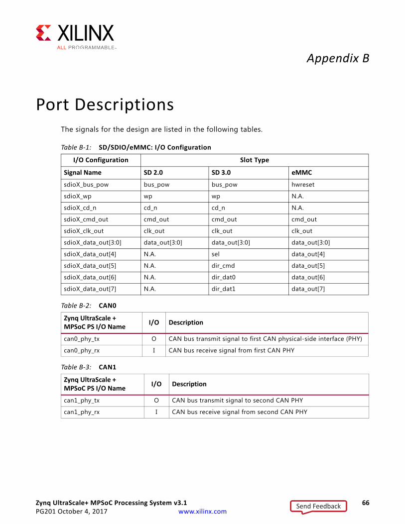
Zynq UltraScale+ MPSoC Processing System v3.1 66PG201 October 4, 2017 www.xilinx.com
Appendix B
Port DescriptionsThe signals for the design are listed in the following tables.
Table B‐1: SD/SDIO/eMMC: I/O Configuration
I/O Configuration Slot Type
Signal Name SD 2.0 SD 3.0 eMMC
sdioX_bus_pow bus_pow bus_pow hwreset
sdioX_wp wp wp N.A.
sdioX_cd_n cd_n cd_n N.A.
sdioX_cmd_out cmd_out cmd_out cmd_out
sdioX_clk_out clk_out clk_out clk_out
sdioX_data_out[3:0] data_out[3:0] data_out[3:0] data_out[3:0]
sdioX_data_out[4] N.A. sel data_out[4]
sdioX_data_out[5] N.A. dir_cmd data_out[5]
sdioX_data_out[6] N.A. dir_dat0 data_out[6]
sdioX_data_out[7] N.A. dir_dat1 data_out[7]
Table B‐2: CAN0
Zynq UltraScale + MPSoC PS I/O Name
I/O Description
can0_phy_tx O CAN bus transmit signal to first CAN physical-side interface (PHY)
can0_phy_rx I CAN bus receive signal from first CAN PHY
Table B‐3: CAN1
Zynq UltraScale + MPSoC PS I/O Name
I/O Description
can1_phy_tx O CAN bus transmit signal to second CAN PHY
can1_phy_rx I CAN bus receive signal from second CAN PHY
Send Feedback
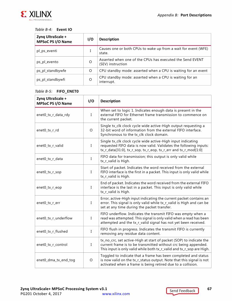
Zynq UltraScale+ MPSoC Processing System v3.1 67PG201 October 4, 2017 www.xilinx.com
Appendix B: Port Descriptions
Table B‐4: Event IO
Zynq UltraScale + MPSoC PS I/O Name
I/O Description
pl_ps_eventi I Causes one or both CPUs to wake up from a wait for event (WFE) state.
ps_pl_evento O Asserted when one of the CPUs has executed the Send EVENT (SEV) instruction
ps_pl_standbywfe O CPU standby mode: asserted when a CPU is waiting for an event
ps_pl_standbywfi O CPU standby mode: asserted when a CPU is waiting for an interrupt.
Table B‐5: FIFO_ENET0
Zynq UltraScale + MPSoC PS I/O Name
I/O Description
enet0_tx_r_data_rdy IWhen set to logic 1. Indicates enough data is present in the external FIFO for Ethernet frame transmission to commence on the current packet.
enet0_tx_r_rd OSingle tx_clk clock cycle wide active-High output requesting a 32-bit word of information from the external FIFO interface. Synchronous to the tx_clk clock domain.
enet0_tx_r_valid ISingle tx_clk clock cycle wide active-High input indicating requested FIFO data is now valid. Validates the following inputs: tx_r_data[31:0], tx_r_sop, tx_r_eop, tx_r_err and tx_r_mod[1:0]
enet0_tx_r_data I FIFO data for transmission; this output is only valid while tx_r_valid is High.
enet0_tx_r_sop IStart of packet. Indicates the word received from the external FIFO interface is the first in a packet. This input is only valid while tx_r_valid is High.
enet0_tx_r_eop IEnd of packet. Indicates the word received from the external FIFO interface is the last in a packet. This input is only valid while tx_r_valid is High.
enet0_tx_r_err IError, active-High input indicating the current packet contains an error. This signal is only valid while tx_r_valid is High and can be set at any time during the packet transfer.
enet0_tx_r_underflow IFIFO underflow. Indicates the transmit FIFO was empty when a read was attempted. This signal is only valid when a read has been attempted and the tx_r_valid signal has not yet been received.
enet0_tx_r_flushed I FIFO flush in progress. Indicates the transmit FIFO is currently removing any residue data content.
enet0_tx_r_control Itx_no_crc, set active-High at start of packet (SOP) to indicate the current frame is to be transmitted without crc being appended. This input is only valid while both tx_r_valid and tx_r_sop are High.
enet0_dma_tx_end_tog OToggled to indicate that a frame has been completed and status is now valid on the tx_r_status output. Note that this signal is not activated when a frame is being retired due to a collision.
Send Feedback

Zynq UltraScale+ MPSoC Processing System v3.1 68PG201 October 4, 2017 www.xilinx.com
Appendix B: Port Descriptions
enet0_dma_tx_status_tog IThis signal must be toggled each time either tx_end_tog or collision_occured are activated. Indicates that the status has been acknowledged.
enet0_tx_r_status O
[3]: fifo_underrun—status output indicating that the Ethernet media access control (MAC) transmitter has underrun due to one of the following conditions. Data under run indicated by tx_r_underflow input from the external FIFO interface during the last frame transfer. Reset once efifo_tx_status_tog changes logic state.
[2]:collision_occured—status output
Indicating that the frame in progress has suffered a collision and that re-transmission of the frame should take place.
[1]: late_coll_occured—status output indicating that the frame in progress suffered a late collision and can be optionally retired.
[0]:too_many_retires—status output indicating the frame in progress experienced excess collisions and was aborted.
enet0_rx_w_wr O Single rx_clk clock cycle wide active-High output indicating a write to the external FIFO interface.
enet0_rx_w_data O Received data for output to the external FIFO interface. This output is only when rx_w_wr is High.
enet0_rx_w_sop OStart of packet. Indicates the word output to the external FIFO interface is the first in a packet. This output is only valid when rx_w_wr is High.
enet0_rx_w_eop OEnd of packet. Indicates the word output to the external FIFO interface is the last in a packet. This output is only valid when rx_w_wr is High.
Table B‐5: FIFO_ENET0 (Cont’d)
Zynq UltraScale + MPSoC PS I/O Name
I/O Description
Send Feedback

Zynq UltraScale+ MPSoC Processing System v3.1 69PG201 October 4, 2017 www.xilinx.com
Appendix B: Port Descriptions
enet0_rx_w_status O
Status signals, valid when rx_w_eop is High and rx_w_err is Low, otherwise driven to zero.
[29]:Rx_w_type_match—indicates the received frame was matched on type ID register
[28]:rx_w_add_match4—indicates the received frame was matched on specific address register4
[27]:rx_w_add_match3—indicates the received frame was matched on specific address register3.
[26]:rx_w_add_match3—indicates the received frame was matched on specific address register2.
[25]:rx_w_add_match3—indicates the received frame was matched on specific address register1.
[24]:rx_w_ext_match—indicates the received frame was matched externally by the eam input pin.
[23]:rx_w_uni_hash_match—indicates the received frame was matched as a unicast hash frame.
[22]:rx_w_mult_hash_match—indicates the received frame was matched as a multicast hash frame.
[21]:rx_w_broadcast_frame—indicates the received frame is a broadcast frame.
[20]:rx_w_prty_tagged—indicates a VLAN priority tag detected with received packet.
[19:16]:rx_w_tci [3:0]—indicates VLAN priority of received packet.
[15]:rx_w_vlan_tagged—indicates VLAN tag detected with received packet.
[14]:rx_w_bad_frame—indicates received packet is bad, or the FIFO has overflowed.
[13:0]: rx_w_frame_length—indicates number of bytes in received packet.
enet0_rx_w_err O
Error, active-High output indicating the current packet contains error. This signal is only valid when both rx_w_wr and rx_w_eop are active-High. Rx_w_err is also set if the frame has not been matched by one of the filters.
enet0_rx_w_overflowI
FIFO overflow. Indicates to the Ethernet MAC that the external RX FIFO has overflowed. The Ethernet MAC uses this signal for status reporting at the end of frame (EOF).
enet0_rx_w_flush O FIFO flush, active-High output indicating that the external RX FIFO must be cleared of all data.
Table B‐5: FIFO_ENET0 (Cont’d)
Zynq UltraScale + MPSoC PS I/O Name
I/O Description
Send Feedback

Zynq UltraScale+ MPSoC Processing System v3.1 70PG201 October 4, 2017 www.xilinx.com
Appendix B: Port Descriptions
Table B‐6: FIFO_ENET1
Zynq UltraScale + MPSoC PS I/O Name
I/O Description
enet1_tx_r_data_rdy IWhen set to logic 1. Indicates enough data is present in the external FIFO for Ethernet frame transmission to commence on the current packet.
enet1_tx_r_rd OSingle tx_clk clock cycle wide active-High output requesting a 32-bit word of information from the external FIFO interface. Synchronous to the tx_clk clock domain.
enet1_tx_r_valid ISingle tx_clk clock cycle wide active-High input indicating requested FIFO data is now valid. Validates the following inputs: tx_r_data[31:0], tx_r_sop, tx_r_eop, tx_r_err and tx_r_mod[1:0].
enet1_tx_r_data I FIFO data for transmission. This output is only valid while tx_r_valid is High.
enet1_tx_r_sop IStart of packet. Indicates the word received from the external FIFO interface is the first in a packet. This input is only valid while tx_r_valid is High.
enet1_tx_r_eop IEnd of packet. Indicates the word received from the external FIFO interface is the last in a packet. This input is only valid while tx_r_valid is High.
enet1_tx_r_err IError, active-High input indicating the current packet contains an error. This signal is only valid while tx_r_valid is High and can be set at any time during the packet transfer.
enet1_tx_r_underflow IFIFO underflow. Indicates the transmit FIFO was empty when a read was attempted. This signal is only valid when a read has been attempted and the tx_r_valid signal has not yet been received.
enet1_tx_r_flushed I FIFO flush in progress. Indicates the transmit FIFO is currently removing any residue data content.
enet1_tx_r_control Itx_no_crc, set active-High at SOP to indicate current frame is to be transmitted without crc being appended. This input is only valid while both tx_r_valid and tx_r_sop are High.
enet1_dma_tx_end_tog OToggled to indicate that a frame has been completed and status is now valid on the tx_r_status output. Note that this signal is not activated when a frame is being retired due to a collision.
enet1_dma_tx_status_tog IThis signal must be toggled each time either tx_end_tog or collision_occured are activated. Indicates that the status has been acknowledged.
Send Feedback

Zynq UltraScale+ MPSoC Processing System v3.1 71PG201 October 4, 2017 www.xilinx.com
Appendix B: Port Descriptions
enet1_tx_r_status O
[3]: fifo_underrun—status output indicating that the Ethernet MAC transmitter has underrun due to one of the following conditions. Data under run indicated by tx_r_underflow input from the external FIFO interface during the last frame transfer. Reset once efifo_tx_status_tog changes logic state.
[2]:collision_occured—status output
Indicating that the frame in progress has suffered a collision and that re-transmission of the frame should take place.
[1]: late_coll_occured—status output indicating that the frame in progress suffered a late collision and can be optionally retired.
[0]:too_many_retires—status output indicating the frame in progress experienced excess collisions and was aborted.
enet1_rx_w_wr O Single rx_clk clock cycle wide active-High output indicating a write to the external FIFO interface.
enet1_rx_w_data O Received data for output to the external FIFO interface. This output is only when rx_w_wr is High.
enet1_rx_w_sop OStart of packet. Indicates the word output to the external FIFO interface is the first in a packet. This output is only valid when rx_w_wr is High.
enet1_rx_w_eop OEnd of packet. Indicates the word output to the external FIFO interface is the last in a packet. This output is only valid when rx_w_wr is High.
Table B‐6: FIFO_ENET1 (Cont’d)
Zynq UltraScale + MPSoC PS I/O Name
I/O Description
Send Feedback
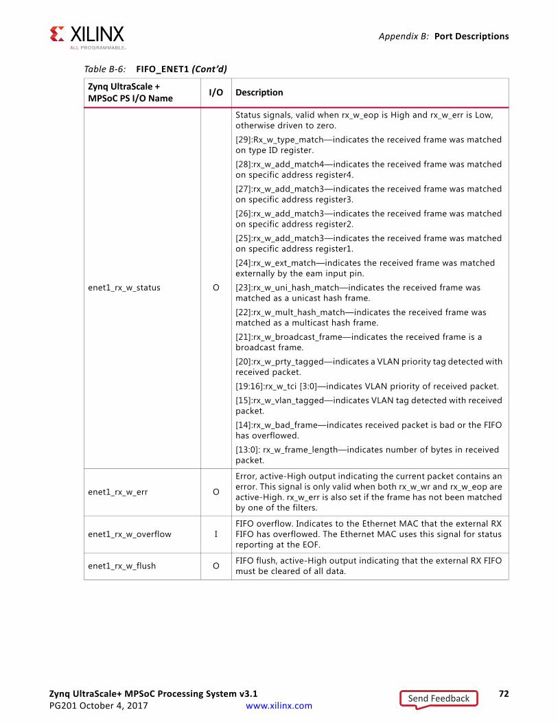
Zynq UltraScale+ MPSoC Processing System v3.1 72PG201 October 4, 2017 www.xilinx.com
Appendix B: Port Descriptions
enet1_rx_w_status O
Status signals, valid when rx_w_eop is High and rx_w_err is Low, otherwise driven to zero.
[29]:Rx_w_type_match—indicates the received frame was matched on type ID register.
[28]:rx_w_add_match4—indicates the received frame was matched on specific address register4.
[27]:rx_w_add_match3—indicates the received frame was matched on specific address register3.
[26]:rx_w_add_match3—indicates the received frame was matched on specific address register2.
[25]:rx_w_add_match3—indicates the received frame was matched on specific address register1.
[24]:rx_w_ext_match—indicates the received frame was matched externally by the eam input pin.
[23]:rx_w_uni_hash_match—indicates the received frame was matched as a unicast hash frame.
[22]:rx_w_mult_hash_match—indicates the received frame was matched as a multicast hash frame.
[21]:rx_w_broadcast_frame—indicates the received frame is a broadcast frame.
[20]:rx_w_prty_tagged—indicates a VLAN priority tag detected with received packet.
[19:16]:rx_w_tci [3:0]—indicates VLAN priority of received packet.
[15]:rx_w_vlan_tagged—indicates VLAN tag detected with received packet.
[14]:rx_w_bad_frame—indicates received packet is bad or the FIFO has overflowed.
[13:0]: rx_w_frame_length—indicates number of bytes in received packet.
enet1_rx_w_err O
Error, active-High output indicating the current packet contains an error. This signal is only valid when both rx_w_wr and rx_w_eop are active-High. rx_w_err is also set if the frame has not been matched by one of the filters.
enet1_rx_w_overflow IFIFO overflow. Indicates to the Ethernet MAC that the external RX FIFO has overflowed. The Ethernet MAC uses this signal for status reporting at the EOF.
enet1_rx_w_flush O FIFO flush, active-High output indicating that the external RX FIFO must be cleared of all data.
Table B‐6: FIFO_ENET1 (Cont’d)
Zynq UltraScale + MPSoC PS I/O Name
I/O Description
Send Feedback
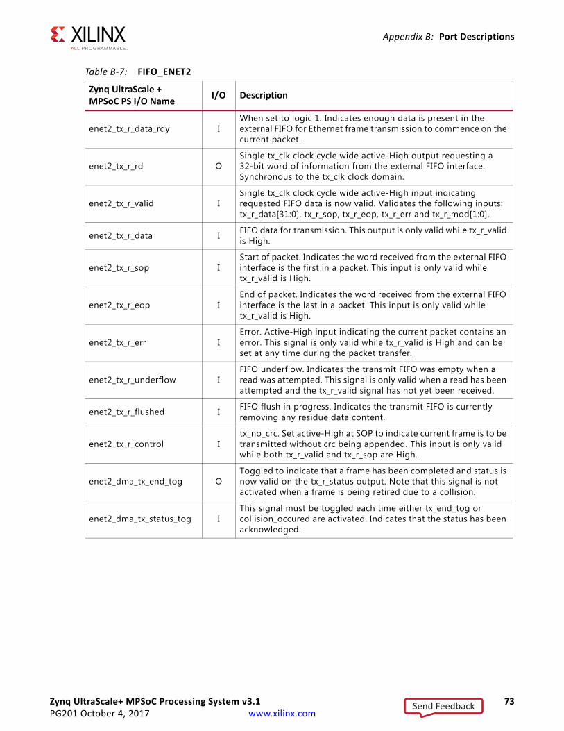
Zynq UltraScale+ MPSoC Processing System v3.1 73PG201 October 4, 2017 www.xilinx.com
Appendix B: Port Descriptions
Table B‐7: FIFO_ENET2
Zynq UltraScale + MPSoC PS I/O Name
I/O Description
enet2_tx_r_data_rdy IWhen set to logic 1. Indicates enough data is present in the external FIFO for Ethernet frame transmission to commence on the current packet.
enet2_tx_r_rd OSingle tx_clk clock cycle wide active-High output requesting a 32-bit word of information from the external FIFO interface. Synchronous to the tx_clk clock domain.
enet2_tx_r_valid ISingle tx_clk clock cycle wide active-High input indicating requested FIFO data is now valid. Validates the following inputs: tx_r_data[31:0], tx_r_sop, tx_r_eop, tx_r_err and tx_r_mod[1:0].
enet2_tx_r_data I FIFO data for transmission. This output is only valid while tx_r_valid is High.
enet2_tx_r_sop IStart of packet. Indicates the word received from the external FIFO interface is the first in a packet. This input is only valid while tx_r_valid is High.
enet2_tx_r_eop IEnd of packet. Indicates the word received from the external FIFO interface is the last in a packet. This input is only valid while tx_r_valid is High.
enet2_tx_r_err IError. Active-High input indicating the current packet contains an error. This signal is only valid while tx_r_valid is High and can be set at any time during the packet transfer.
enet2_tx_r_underflow IFIFO underflow. Indicates the transmit FIFO was empty when a read was attempted. This signal is only valid when a read has been attempted and the tx_r_valid signal has not yet been received.
enet2_tx_r_flushed I FIFO flush in progress. Indicates the transmit FIFO is currently removing any residue data content.
enet2_tx_r_control Itx_no_crc. Set active-High at SOP to indicate current frame is to be transmitted without crc being appended. This input is only valid while both tx_r_valid and tx_r_sop are High.
enet2_dma_tx_end_tog OToggled to indicate that a frame has been completed and status is now valid on the tx_r_status output. Note that this signal is not activated when a frame is being retired due to a collision.
enet2_dma_tx_status_tog IThis signal must be toggled each time either tx_end_tog or collision_occured are activated. Indicates that the status has been acknowledged.
Send Feedback

Zynq UltraScale+ MPSoC Processing System v3.1 74PG201 October 4, 2017 www.xilinx.com
Appendix B: Port Descriptions
enet2_tx_r_status O
[3]: fifo_underrun—status output indicating that the Ethernet MAC transmitter has under run due to one of the following conditions. Data under run indicated by tx_r_underflow input from the external FIFO interface during the last frame transfer. Reset once efifo_tx_status_tog changes logic state.
[2]:collision_occured—status output
Indicating that the frame in progress has suffered a collision and that re-transmission of the frame should take place.
[1]: late_coll_occured—status output indicating that the frame in progress suffered a late collision and can be optionally retired.
[0]:too_many_retires—status output indicating the frame in progress experienced excess collisions and was aborted.
enet2_rx_w_wr O Single rx_clk clock cycle wide active-High output indicating a write to the external FIFO interface.
enet2_rx_w_data O Received data for output to the external FIFO interface. This output is only when rx_w_wr is High.
enet2_rx_w_sop OStart of packet. Indicates the word output to the external FIFO interface is the first in a packet. This output is only valid when rx_w_wr is High.
enet2_rx_w_eop OEnd of packet. Indicates the word output to the external FIFO interface is the last in a packet. This output is only valid when rx_w_wr is High.
Table B‐7: FIFO_ENET2 (Cont’d)
Zynq UltraScale + MPSoC PS I/O Name
I/O Description
Send Feedback
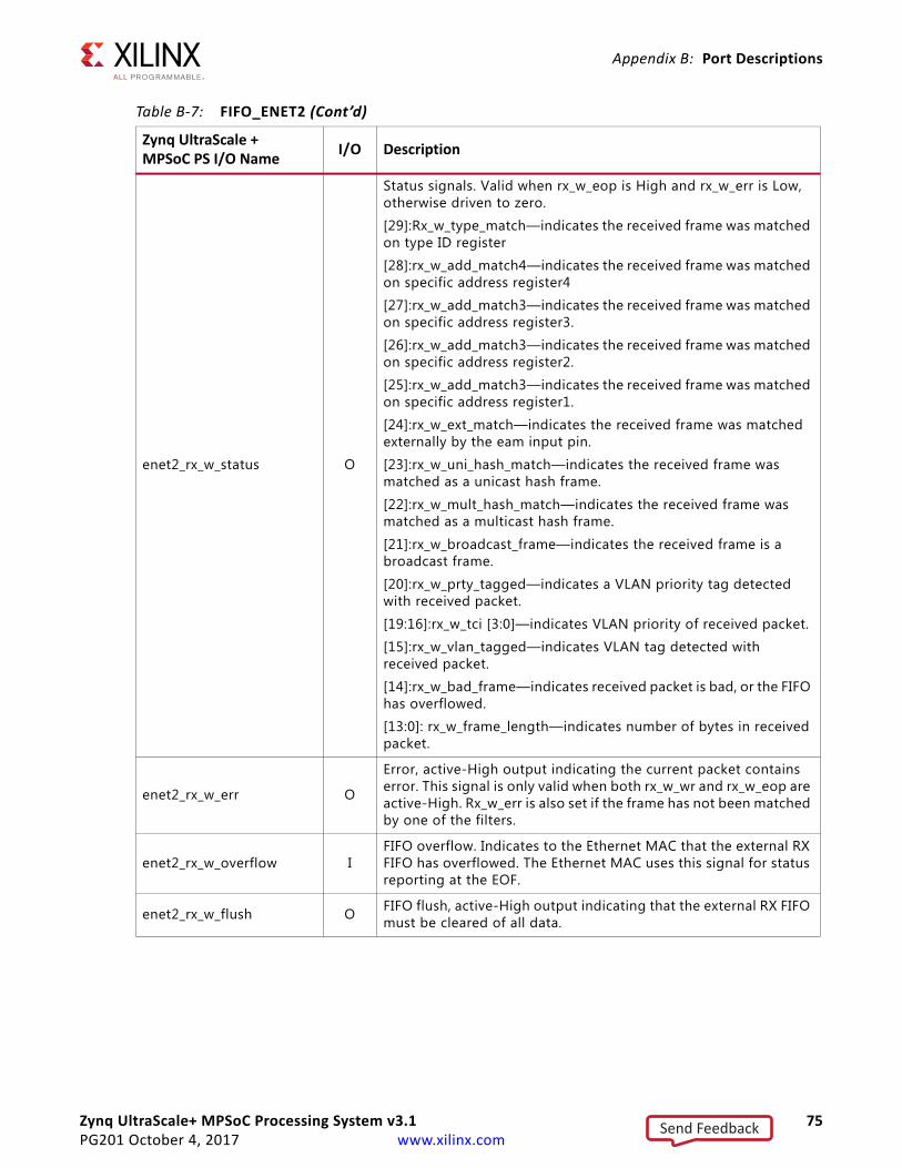
Zynq UltraScale+ MPSoC Processing System v3.1 75PG201 October 4, 2017 www.xilinx.com
Appendix B: Port Descriptions
enet2_rx_w_status O
Status signals. Valid when rx_w_eop is High and rx_w_err is Low, otherwise driven to zero.
[29]:Rx_w_type_match—indicates the received frame was matched on type ID register
[28]:rx_w_add_match4—indicates the received frame was matched on specific address register4
[27]:rx_w_add_match3—indicates the received frame was matched on specific address register3.
[26]:rx_w_add_match3—indicates the received frame was matched on specific address register2.
[25]:rx_w_add_match3—indicates the received frame was matched on specific address register1.
[24]:rx_w_ext_match—indicates the received frame was matched externally by the eam input pin.
[23]:rx_w_uni_hash_match—indicates the received frame was matched as a unicast hash frame.
[22]:rx_w_mult_hash_match—indicates the received frame was matched as a multicast hash frame.
[21]:rx_w_broadcast_frame—indicates the received frame is a broadcast frame.
[20]:rx_w_prty_tagged—indicates a VLAN priority tag detected with received packet.
[19:16]:rx_w_tci [3:0]—indicates VLAN priority of received packet.
[15]:rx_w_vlan_tagged—indicates VLAN tag detected with received packet.
[14]:rx_w_bad_frame—indicates received packet is bad, or the FIFO has overflowed.
[13:0]: rx_w_frame_length—indicates number of bytes in received packet.
enet2_rx_w_err O
Error, active-High output indicating the current packet contains error. This signal is only valid when both rx_w_wr and rx_w_eop are active-High. Rx_w_err is also set if the frame has not been matched by one of the filters.
enet2_rx_w_overflow IFIFO overflow. Indicates to the Ethernet MAC that the external RX FIFO has overflowed. The Ethernet MAC uses this signal for status reporting at the EOF.
enet2_rx_w_flush O FIFO flush, active-High output indicating that the external RX FIFO must be cleared of all data.
Table B‐7: FIFO_ENET2 (Cont’d)
Zynq UltraScale + MPSoC PS I/O Name
I/O Description
Send Feedback

Zynq UltraScale+ MPSoC Processing System v3.1 76PG201 October 4, 2017 www.xilinx.com
Appendix B: Port Descriptions
Table B‐8: FIFO_ENET3
Zynq UltraScale + MPSoC PS I/O Name
I/O Description
enet3_tx_r_data_rdy IWhen set to logic 1, indicates enough data is present in the external FIFO for Ethernet frame transmission to commence on the current packet.
enet3_tx_r_rd OSingle tx_clk clock cycle wide. Active-High output requesting a 32-bit word of information from the external FIFO interface. Synchronous to the tx_clk clock domain.
enet3_tx_r_valid ISingle tx_clk clock cycle wide. Active-High input indicating requested FIFO data is now valid. Validates the following inputs: tx_r_data[31:0], tx_r_sop, tx_r_eop, tx_r_err and tx_r_mod[1:0]
enet3_tx_r_data I FIFO data for transmission. This output is only valid while tx_r_valid is High.
enet3_tx_r_sop IStart of packet. Indicates the word received from the external FIFO interface is the first in a packet. This input is only valid while tx_r_valid is High.
enet3_tx_r_eop IEnd of packet. Indicates the word received from the external FIFO interface is the last in a packet. This input is only valid while tx_r_valid is High.
enet3_tx_r_err IError. Active-High input indicating the current packet contains an error. This signal is only valid while tx_r_valid is High and can be set at any time during the packet transfer.
enet3_tx_r_underflow IFIFO underflow. Indicates the transmit FIFO was empty when a read was attempted. This signal is only valid when a read has been attempted and the tx_r_valid signal has not yet been received.
enet3_tx_r_flushed I FIFO flush in progress. Indicates the transmit FIFO is currently removing any residue data content.
enet3_tx_r_control Itx_no_crc. Set active-High at SOP to indicate current frame is to be transmitted without crc being appended. This input is only valid while both tx_r_valid and tx_r_sop are High.
enet3_dma_tx_end_tog OToggled to indicate that a frame has been completed and status is now valid on the tx_r_status output. Note that this signal is not activated when a frame is being retired due to a collision.
enet3_dma_tx_status_tog IThis signal must be toggled each time either tx_end_tog or collision_occured are activated. Indicates that the status has been acknowledged.
Send Feedback

Zynq UltraScale+ MPSoC Processing System v3.1 77PG201 October 4, 2017 www.xilinx.com
Appendix B: Port Descriptions
enet3_tx_r_status O
[3]: fifo_underrun—status output indicating that the Ethernet MAC transmitter has under-run due to one of the following conditions. Data under run indicated by tx_r_underflow input from the external FIFO interface during the last frame transfer. Reset once efifo_tx_status_tog changes logic state.
[2]:collision_occured—status output
Indicating that the frame in progress has suffered a collision and that re-transmission of the frame should take place.
[1]: late_coll_occured—status output indicating that the frame in progress suffered a late collision and can be optionally retired.
[0]:too_many_retires—status output indicating the frame in progress experienced excess collisions and was aborted.
enet3_rx_w_wr O Single rx_clk clock cycle wide active-High output indicating a write to the external FIFO interface.
enet3_rx_w_data O Received data for output to the external FIFO interface. This output is only when rx_w_wr is High.
enet3_rx_w_sop OStart of packet. Indicates the word output to the external FIFO interface is the first in a packet. This output is only valid when rx_w_wr is High.
enet3_rx_w_eop OEnd of packet. Indicates the word output to the external FIFO interface is the last in a packet. This output is only valid when rx_w_wr is High.
Table B‐8: FIFO_ENET3 (Cont’d)
Zynq UltraScale + MPSoC PS I/O Name
I/O Description
Send Feedback

Zynq UltraScale+ MPSoC Processing System v3.1 78PG201 October 4, 2017 www.xilinx.com
Appendix B: Port Descriptions
enet3_rx_w_status O
Status signals. Valid when rx_w_eop is High and rx_w_err is Low, otherwise driven to zero.
[29]:Rx_w_type_match—indicates the received frame was matched on type ID register.
[28]:rx_w_add_match4—indicates the received frame was matched on specific address register4.
[27]:rx_w_add_match3—indicates the received frame was matched on specific address register3.
[26]:rx_w_add_match3—indicates the received frame was matched on specific address register2.
[25]:rx_w_add_match3—indicates the received frame was matched on specific address register1.
[24]:rx_w_ext_match—indicates the received frame was matched externally by the eam input pin.
[23]:rx_w_uni_hash_match—indicates the received frame was matched as a unicast hash frame.
[22]:rx_w_mult_hash_match—indicates the received frame was matched as a multicast hash frame.
[21]:rx_w_broadcast_frame—indicates the received frame is a broadcast frame.
[20]:rx_w_prty_tagged—indicates a VLAN priority tag detected with received packet.
[19:16]:rx_w_tci [3:0]—indicates VLAN priority of received packet.
[15]:rx_w_vlan_tagged—indicates VLAN tag detected with received packet.
[14]:rx_w_bad_frame—indicates received packet is bad, or the FIFO has overflowed.
[13:0]: rx_w_frame_length—indicates number of bytes in received packet.
enet3_rx_w_err O
Error. Active-High output indicating the current packet contains error. This signal is only valid when both rx_w_wr and rx_w_eop are active-High. Rx_w_err is also set if the frame has not been matched by one of the filters.
enet3_rx_w_overflow IFIFO overflow. Indicates to the Ethernet MAC that the external RX FIFO has overflowed. The Ethernet MAC uses this signal for status reporting at the EOF.
enet3_rx_w_flush O FIFO flush, active-High output indicating that the external RX FIFO must be cleared of all data.
Table B‐8: FIFO_ENET3 (Cont’d)
Zynq UltraScale + MPSoC PS I/O Name
I/O Description
Send Feedback

Zynq UltraScale+ MPSoC Processing System v3.1 79PG201 October 4, 2017 www.xilinx.com
Appendix B: Port Descriptions
Table B‐9: FTM
Zynq UltraScale + MPSoC PS I/O Name
I/O Description
pl_ps_trigack I Trigger acknowledgement from PL
pl_ps_trigger O Trigger output to PL
ps_pl_trigack O Trigger acknowledgement to PL
ps_pl_trigger I Trigger input from PL
gpo O General purpose output
gpi I General purpose input
Table B‐10: TSU
Zynq UltraScale + MPSoC PS I/O Name
I/O Description
emio_enetx_tsu_inc_ctrl I TSU increment control
fmio_gem_tsu_clk_from_pl I TSU clock source from PL
emio_enetx_tsu_timer_cmp_val O TSU timer compare value
emio_enet0_enet_tsu_timer_cnt O TSU timer count value
Table B‐11: GMII_ENET0
Zynq UltraScale + MPSoC PS I/O Name
I/O Description
enet0_gmii_rx_clk I GEM 0 Receive clock to the system clock generator
enet0_speed_mode O Indicates speed and external interface that the GEM is currently configured to use to the system clock generator
enet0_gmii_crs I Carrier sense from the PHY
enet0_gmii_col I Collision detect from the PHY
enet0_gmii_rxd I Receive data from the PHY
enet0_gmii_rx_er I Receive error signal from the PHY
enet0_gmii_rx_dv I Receive data valid signal from the PHY
enet0_gmii_tx_clk I GEM 0 Transmit clock from the system clock generator
enet0_gmii_txd O Transmit data to the PHY
enet0_gmii_tx_en O Transmit enable to the PHY
enet0_gmii_tx_er O Transmit error signal to the PHY. Asserted if the DMA block fails to fetch data from memory during frame transmission.
Send Feedback
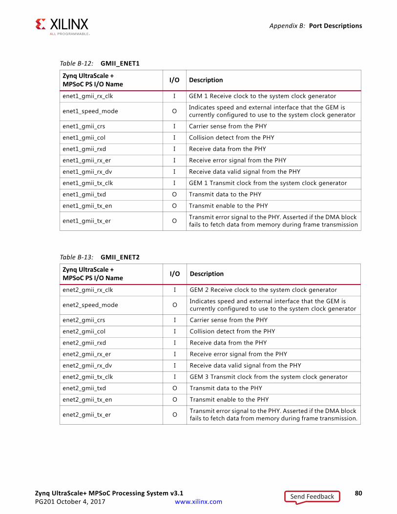
Zynq UltraScale+ MPSoC Processing System v3.1 80PG201 October 4, 2017 www.xilinx.com
Appendix B: Port Descriptions
Table B‐12: GMII_ENET1
Zynq UltraScale + MPSoC PS I/O Name
I/O Description
enet1_gmii_rx_clk I GEM 1 Receive clock to the system clock generator
enet1_speed_mode O Indicates speed and external interface that the GEM is currently configured to use to the system clock generator
enet1_gmii_crs I Carrier sense from the PHY
enet1_gmii_col I Collision detect from the PHY
enet1_gmii_rxd I Receive data from the PHY
enet1_gmii_rx_er I Receive error signal from the PHY
enet1_gmii_rx_dv I Receive data valid signal from the PHY
enet1_gmii_tx_clk I GEM 1 Transmit clock from the system clock generator
enet1_gmii_txd O Transmit data to the PHY
enet1_gmii_tx_en O Transmit enable to the PHY
enet1_gmii_tx_er O Transmit error signal to the PHY. Asserted if the DMA block fails to fetch data from memory during frame transmission
Table B‐13: GMII_ENET2
Zynq UltraScale + MPSoC PS I/O Name
I/O Description
enet2_gmii_rx_clk I GEM 2 Receive clock to the system clock generator
enet2_speed_mode O Indicates speed and external interface that the GEM is currently configured to use to the system clock generator
enet2_gmii_crs I Carrier sense from the PHY
enet2_gmii_col I Collision detect from the PHY
enet2_gmii_rxd I Receive data from the PHY
enet2_gmii_rx_er I Receive error signal from the PHY
enet2_gmii_rx_dv I Receive data valid signal from the PHY
enet2_gmii_tx_clk I GEM 3 Transmit clock from the system clock generator
enet2_gmii_txd O Transmit data to the PHY
enet2_gmii_tx_en O Transmit enable to the PHY
enet2_gmii_tx_er O Transmit error signal to the PHY. Asserted if the DMA block fails to fetch data from memory during frame transmission.
Send Feedback

Zynq UltraScale+ MPSoC Processing System v3.1 81PG201 October 4, 2017 www.xilinx.com
Appendix B: Port Descriptions
Table B‐14: GMII_ENET3
Zynq UltraScale + MPSoC PS I/O Name
I/O Description
enet3_gmii_rx_clk I GEM 3 Receive clock to the system clock generator
enet3_speed_mode O Indicates speed and external interface that the GEM is currently configured to use to the system clock generator.
enet3_gmii_crs I Carrier sense from the PHY
enet3_gmii_col I Collision detect from the PHY
enet3_gmii_rxd I Receive data from the PHY
enet3_gmii_rx_er I Receive error signal from the PHY
enet3_gmii_rx_dv I Receive data valid signal from the PHY
enet3_gmii_tx_clk I GEM 3 Transmit clock from the system clock generator
enet3_gmii_txd O Transmit data to the PHY
enet3_gmii_tx_en O Transmit enable to the PHY
enet3_gmii_tx_er O Transmit error signal to the PHY. Asserted if the DMA block fails to fetch data from memory during frame transmission.
Table B‐15: GPIO_0
Zynq UltraScale + MPSoC PS I/O Name
I/O Description
gpio_i I GPIO port input
gpio_o O GPIO port output
gpio_t O 3-state enable signal for GPIO port
Table B‐16: IIC0
Zynq UltraScale + MPSoC PS I/O Name
I/O Description
i2c0_scl_i I Actual state of the external serial clock (SCL) clock signal
i2c0_scl_o O Clock level to be placed on SCL pin
i2c0_scl_t O3-state enable for the SCL output buffer.
This signal has a direct connection to i2c0_scl_oe.
i2c0_sda_i I Actual state of the external serial data (SDA) signal
i2c0_sda_o O Data bit to be placed on external SDA signal
i2c0_sda_t O 3-state enable for the SDA output buffer This signal has a direct connection to i2c0_sda_oe.
Send Feedback
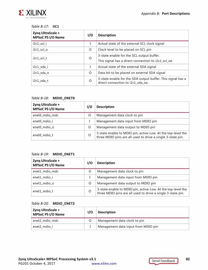
Zynq UltraScale+ MPSoC Processing System v3.1 82PG201 October 4, 2017 www.xilinx.com
Appendix B: Port Descriptions
Table B‐17: IIC1
Zynq UltraScale + MPSoC PS I/O Name
I/O Description
i2c1_scl_i I Actual state of the external SCL clock signal
i2c1_scl_o O Clock level to be placed on SCL pin
i2c1_scl_t O3-state enable for the SCL output buffer.
This signal has a direct connection to i2c1_scl_oe.
i2c1_sda_i I Actual state of the external SDA signal
i2c1_sda_o O Data bit to be placed on external SDA signal
i2c1_sda_t O 3-state enable for the SDA output buffer. This signal has a direct connection to i2c1_sda_oe.
Table B‐18: MDIO_ENET0
Zynq UltraScale + MPSoC PS I/O Name
I/O Description
enet0_mdio_mdc O Management data clock to pin
enet0_mdio_i I Management data input from MDIO pin
enet0_mdio_o O Management data output to MDIO pin
enet0_mdio_t O 3-state enable to MDIO pin, active-Low. At the top-level the three MDIO pins are all used to drive a single 3-state pin.
Table B‐19: MDIO_ENET1
Zynq UltraScale + MPSoC PS I/O Name
I/O Description
enet1_mdio_mdc O Management data clock to pin
enet1_mdio_i I Management data input from MDIO pin
enet1_mdio_o O Management data output to MDIO pin
enet1_mdio_t O 3-state enable to MDIO pin, active-Low. At the top-level the three MDIO pins are all used to drive a single 3-state pin.
Table B‐20: MDIO_ENET2
Zynq UltraScale + MPSoC PS I/O Name
I/O Description
enet2_mdio_mdc O Management data clock to pin
enet2_mdio_i I Management data input from MDIO pin
Send Feedback

Zynq UltraScale+ MPSoC Processing System v3.1 83PG201 October 4, 2017 www.xilinx.com
Appendix B: Port Descriptions
enet2_mdio_o O Management data output to MDIO pin
enet2_mdio_t O 3-state enable to MDIO pin, active-Low. At the top-level the three MDIO pins are all used to drive a single 3-state pin.
Table B‐21: MDIO_ENET3
Zynq UltraScale + MPSoC PS I/O Name
I/O Description
enet3_mdio_mdc O Management data clock to pin
enet3_mdio_i I Management data input from MDIO pin
enet3_mdio_o O Management data output to MDIO pin
enet3_mdio_t O 3-state enable to MDIO pin, active-Low. At the top-level the three MDIO pins are all used to drive a single 3-state pin.
Table B‐22: PL_CLK0
Zynq UltraScale + MPSoC PS I/O Name
I/O Description
pl_clk0 O PL Clock 0
Table B‐23: PL_CLK1
Zynq UltraScale + MPSoC PS I/O Name
I/O Description
pl_clk1 O PL Clock 1
Table B‐24: PL_CLK2
Zynq UltraScale + MPSoC PS I/O Name
I/O Description
pl_clk2 O PL Clock 2
Table B‐25: PL_CLK3
Zynq UltraScale + MPSoC PS I/O Name
I/O Description
pl_clk3 O PL Clock 3
Table B‐20: MDIO_ENET2 (Cont’d)
Zynq UltraScale + MPSoC PS I/O Name
I/O Description
Send Feedback
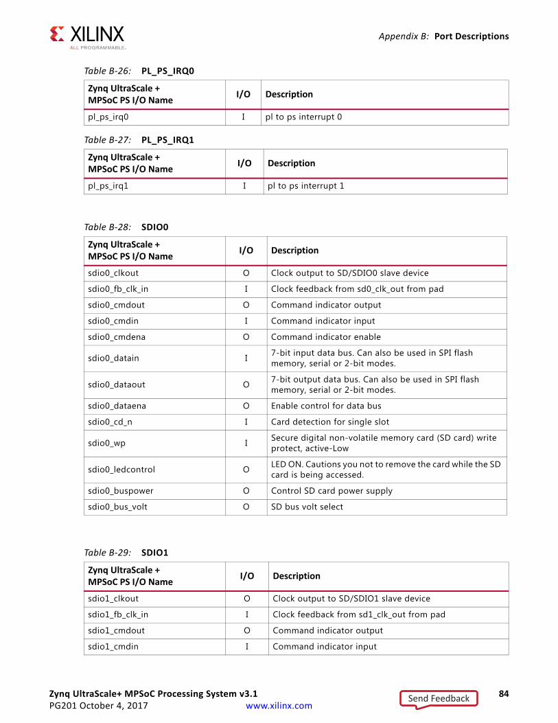
Zynq UltraScale+ MPSoC Processing System v3.1 84PG201 October 4, 2017 www.xilinx.com
Appendix B: Port Descriptions
Table B‐26: PL_PS_IRQ0
Zynq UltraScale + MPSoC PS I/O Name
I/O Description
pl_ps_irq0 I pl to ps interrupt 0
Table B‐27: PL_PS_IRQ1
Zynq UltraScale + MPSoC PS I/O Name
I/O Description
pl_ps_irq1 I pl to ps interrupt 1
Table B‐28: SDIO0
Zynq UltraScale + MPSoC PS I/O Name
I/O Description
sdio0_clkout O Clock output to SD/SDIO0 slave device
sdio0_fb_clk_in I Clock feedback from sd0_clk_out from pad
sdio0_cmdout O Command indicator output
sdio0_cmdin I Command indicator input
sdio0_cmdena O Command indicator enable
sdio0_datain I 7-bit input data bus. Can also be used in SPI flash memory, serial or 2-bit modes.
sdio0_dataout O 7-bit output data bus. Can also be used in SPI flash memory, serial or 2-bit modes.
sdio0_dataena O Enable control for data bus
sdio0_cd_n I Card detection for single slot
sdio0_wp I Secure digital non-volatile memory card (SD card) write protect, active-Low
sdio0_ledcontrol O LED ON. Cautions you not to remove the card while the SD card is being accessed.
sdio0_buspower O Control SD card power supply
sdio0_bus_volt O SD bus volt select
Table B‐29: SDIO1
Zynq UltraScale + MPSoC PS I/O Name
I/O Description
sdio1_clkout O Clock output to SD/SDIO1 slave device
sdio1_fb_clk_in I Clock feedback from sd1_clk_out from pad
sdio1_cmdout O Command indicator output
sdio1_cmdin I Command indicator input
Send Feedback

Zynq UltraScale+ MPSoC Processing System v3.1 85PG201 October 4, 2017 www.xilinx.com
Appendix B: Port Descriptions
sdio1_cmdena O Command indicator enable
sdio1_datain I 7-bit input data bus. Can also be used in SPI flash memory, serial or 2-bit modes.
sdio1_dataout O 7-bit output data bus. Can also be used in SPI flash memory, serial or 2-bit modes.
sdio1_dataena O Enable control for data bus
sdio1_cd_n I Card detection for single slot
sdio1_wp I SD card write protect, active-Low
sdio1_ledcontrol O LED ON: Cautions you not to remove the card while the SD card is being accessed.
sdio1_bus_power O Control SD card power supply
sdio1_bus_volt O SD bus volt select
Table B‐30: SPI0
Zynq UltraScale + MPSoC PS I/O Name
I/O Description
spi0_sclk_i I SPI flash memory slave clock
spi0_sclk_o O SPI flash memory master clock output
spi0_sclk_t OSPI flash memory clock 3-state enable, active-Low.
This signal is a version of spi0_n_sclk_en.
spi0_m_i I SPI flash memory master in slave out (MISO) signal, master input
spi0_m_o OSPI flash memory master out slave in
(MOSI) signal, master output
spi0_mo_t OSPI flash memory MOSI signal, 3-state enable, active-Low.
This signal is a version of spi0_n_mo_en.
spi0_s_i I SPI flash memory MOSI signal, slave input
spi0_s_o O SPI flash memory MISO signal, slave output
spi0_n_ss_o_n O SPI flash memory slave select outputs
spi0_ss_n_t OSPI flash memory slave select 3-state enable, active-Low.
This signal is a version of spi0_n_ss_en.
Table B‐29: SDIO1 (Cont’d)
Zynq UltraScale + MPSoC PS I/O Name
I/O Description
Send Feedback

Zynq UltraScale+ MPSoC Processing System v3.1 86PG201 October 4, 2017 www.xilinx.com
Appendix B: Port Descriptions
Table B‐31: SPI1
Zynq UltraScale + MPSoC PS I/O Name
I/O Description
spi1_sclk_i ISPI flash memory slave clock.
Can be passed directly from pin if low speed (< 50 MHz).
spi1_sclk_o OSPI flash memory master clock output.
Can be passed directly to pin if low speed (< 50 MHz).
spi1_sclk_t OSPI flash memory clock 3-state enable, active-Low.
This signal is a version of spi1_n_sclk_en
spi1_m_i I SPI flash memory MISO signal, master input
spi1_m_o O SPI flash memory MOSI signal, master output
spi1_mo_t O SPI flash memory MOSI signal, 3-state enable, active-Low. This signal is a version of spi1_n_mo_en.
spi1_s_i I SPI flash memory MOSI signal, slave input
spi1_s_o O SPI flash memory MISO signal, slave output
spi1_n_ss_o_n O SPI flash memory peripheral select outputs
spi1_ss_n_t OSPI flash memory slave select 3-state enable, active-Low.
This signal is a version of spi1_n_ss_en.
Table B‐32: Trace0
Zynq UltraScale + MPSoC PS I/O Name
I/O Description
tracectl O Trace control
tracedata O Trace data
Table B‐33: UART0
Zynq UltraScale + MPSoC PS I/O Name
I/O Description
uart0_ctsn I Clear-to-send flow control
uart0_rtsn O Request-to-send flow control
uart0_dsrn I Modem data set ready
uart0_dcdn I Modem data carrier detect
uart0_rin I Modem ring indicator
uart0_dtrn O Modem data terminal ready
Send Feedback

Zynq UltraScale+ MPSoC Processing System v3.1 87PG201 October 4, 2017 www.xilinx.com
Appendix B: Port Descriptions
Table B‐34: UART1
Zynq UltraScale + MPSoC PS I/O Name
I/O Description
uart1_ctsn I Clear-to-send flow control
uart1_rtsn O Request-to-send flow control
uart1_dsrn I Modem data set ready
uart1_dcdn I Modem data carrier detect
uart1_rin I Modem ring indicator
uart1_dtrn O Modem data terminal ready
Table B‐35: TTC0
Zynq UltraScale + MPSoC PS I/O Name
I/O Description
ttc0_wave_o O Triple timer counter (TTC) clock (Waveform generated)
ttc0_clk_i I TTC0 clock input
Table B‐36: TTC1
Zynq UltraScale + MPSoC PS I/O Name
I/O Description
ttc1_wave_o O TTC clock (Waveform generated)
ttc1_clk_i I TTC1 clock input
Table B‐37: TTC2
Zynq UltraScale + MPSoC PS I/O Name
I/O Description
ttc3_wave_o O TTC clock (Waveform generated)
ttc2_clk_i I TTC2 clock input
Table B‐38: TTC3
Zynq UltraScale + MPSoC PS I/O Name
I/O Description
ttc3_wave_o O TTC clock (Waveform generated)
ttc3_clk_i I TTC3 clock input
Send Feedback

Zynq UltraScale+ MPSoC Processing System v3.1 88PG201 October 4, 2017 www.xilinx.com
Appendix B: Port Descriptions
Table B‐39: WDT0
Zynq UltraScale + MPSoC PS I/O Name
I/O Description
wdt0_clk_i I WDT0 clock input
wdt0_rst_o O WDT0 reset
Table B‐40: WDT1
Zynq UltraScale + MPSoC PS I/O Name
I/O Description
wdt1_clk_i I WDT1 clock input
wdt1_rst_o O WDT1 reset
Table B‐41: Interrupt Signals
Zynq UltraScale + MPSoC PS I/O Name
I/O Description
ps_pl_irq_can0 O CAN0 interrupt
ps_pl_irq_can1 O CAN1 interrupt
ps_pl_irq_enet0 O Ethernet0 interrupt
ps_pl_irq_enet1 O Gigabit ethernet1 interrupt
ps_pl_irq_enet2 O Gigabit ethernet2 interrupt
ps_pl_irq_enet3 O Gigabit ethernet3 interrupt
ps_pl_irq_enet0_wake0 O Ethernet0 wake-up interrupt
ps_pl_irq_enet0_wake1 O Gigabit ethernet1 wake-up interrupt
ps_pl_irq_enet0_wake2 O Gigabit ethernet2 wake-up interrupt
ps_pl_irq_enet0_wake3 O Gigabit ethernet3 wake-up interrupt
ps_pl_irq_gpio O GPIO interrupt
ps_pl_irq_i2c0 O I2C0 interrupt
ps_pl_irq_i2c1 O I2C1 interrupt
ps_pl_irq_uart0 O UART0 interrupt
ps_pl_irq_uart1 O UART1 interrupt
ps_pl_irq_sdio0 O SDIO0 interrupt
ps_pl_irq_sdio1 O SDIO1 interrupt
ps_pl_irq_sdio0_wake O SDIO0 wake interrupt
ps_pl_irq_sdio1_wake O SDIO1 wake interrupt
ps_pl_irq_spi0 O SPI0 interrupt
ps_pl_irq_spi1 O SPI1 interrupt
Send Feedback
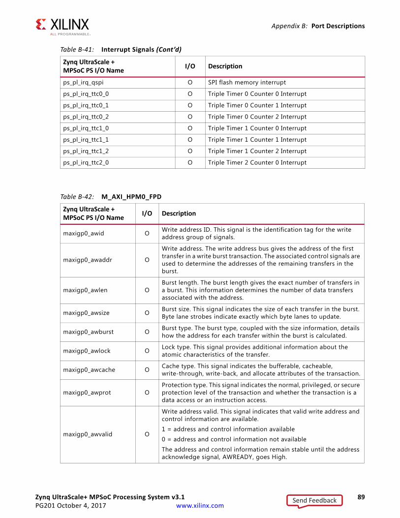
Zynq UltraScale+ MPSoC Processing System v3.1 89PG201 October 4, 2017 www.xilinx.com
Appendix B: Port Descriptions
ps_pl_irq_qspi O SPI flash memory interrupt
ps_pl_irq_ttc0_0 O Triple Timer 0 Counter 0 Interrupt
ps_pl_irq_ttc0_1 O Triple Timer 0 Counter 1 Interrupt
ps_pl_irq_ttc0_2 O Triple Timer 0 Counter 2 Interrupt
ps_pl_irq_ttc1_0 O Triple Timer 1 Counter 0 Interrupt
ps_pl_irq_ttc1_1 O Triple Timer 1 Counter 1 Interrupt
ps_pl_irq_ttc1_2 O Triple Timer 1 Counter 2 Interrupt
ps_pl_irq_ttc2_0 O Triple Timer 2 Counter 0 Interrupt
Table B‐42: M_AXI_HPM0_FPD
Zynq UltraScale + MPSoC PS I/O Name
I/O Description
maxigp0_awid O Write address ID. This signal is the identification tag for the write address group of signals.
maxigp0_awaddr O
Write address. The write address bus gives the address of the first transfer in a write burst transaction. The associated control signals are used to determine the addresses of the remaining transfers in the burst.
maxigp0_awlen OBurst length. The burst length gives the exact number of transfers in a burst. This information determines the number of data transfers associated with the address.
maxigp0_awsize O Burst size. This signal indicates the size of each transfer in the burst. Byte lane strobes indicate exactly which byte lanes to update.
maxigp0_awburst O Burst type. The burst type, coupled with the size information, details how the address for each transfer within the burst is calculated.
maxigp0_awlock O Lock type. This signal provides additional information about the atomic characteristics of the transfer.
maxigp0_awcache O Cache type. This signal indicates the bufferable, cacheable, write-through, write-back, and allocate attributes of the transaction.
maxigp0_awprot OProtection type. This signal indicates the normal, privileged, or secure protection level of the transaction and whether the transaction is a data access or an instruction access.
maxigp0_awvalid O
Write address valid. This signal indicates that valid write address and control information are available.
1 = address and control information available
0 = address and control information not available
The address and control information remain stable until the address acknowledge signal, AWREADY, goes High.
Table B‐41: Interrupt Signals (Cont’d)
Zynq UltraScale + MPSoC PS I/O Name
I/O Description
Send Feedback
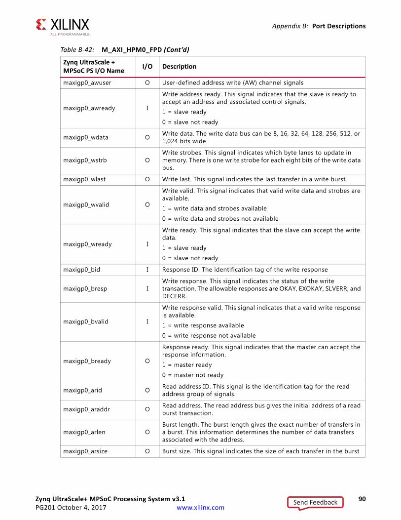
Zynq UltraScale+ MPSoC Processing System v3.1 90PG201 October 4, 2017 www.xilinx.com
Appendix B: Port Descriptions
maxigp0_awuser O User-defined address write (AW) channel signals
maxigp0_awready I
Write address ready. This signal indicates that the slave is ready to accept an address and associated control signals.
1 = slave ready
0 = slave not ready
maxigp0_wdata O Write data. The write data bus can be 8, 16, 32, 64, 128, 256, 512, or 1,024 bits wide.
maxigp0_wstrb OWrite strobes. This signal indicates which byte lanes to update in memory. There is one write strobe for each eight bits of the write data bus.
maxigp0_wlast O Write last. This signal indicates the last transfer in a write burst.
maxigp0_wvalid O
Write valid. This signal indicates that valid write data and strobes are available.
1 = write data and strobes available
0 = write data and strobes not available
maxigp0_wready I
Write ready. This signal indicates that the slave can accept the write data.
1 = slave ready
0 = slave not ready
maxigp0_bid I Response ID. The identification tag of the write response
maxigp0_bresp IWrite response. This signal indicates the status of the write transaction. The allowable responses are OKAY, EXOKAY, SLVERR, and DECERR.
maxigp0_bvalid I
Write response valid. This signal indicates that a valid write response is available.
1 = write response available
0 = write response not available
maxigp0_bready O
Response ready. This signal indicates that the master can accept the response information.
1 = master ready
0 = master not ready
maxigp0_arid O Read address ID. This signal is the identification tag for the read address group of signals.
maxigp0_araddr O Read address. The read address bus gives the initial address of a read burst transaction.
maxigp0_arlen OBurst length. The burst length gives the exact number of transfers in a burst. This information determines the number of data transfers associated with the address.
maxigp0_arsize O Burst size. This signal indicates the size of each transfer in the burst
Table B‐42: M_AXI_HPM0_FPD (Cont’d)
Zynq UltraScale + MPSoC PS I/O Name
I/O Description
Send Feedback

Zynq UltraScale+ MPSoC Processing System v3.1 91PG201 October 4, 2017 www.xilinx.com
Appendix B: Port Descriptions
maxigp0_arburst O Burst type. The burst type, coupled with the size information, details how the address for each transfer within the burst is calculated.
maxigp0_arlock O Lock type. This signal provides additional information about the atomic characteristics of the transfer.
maxigp0_arcache O Cache type. This signal provides additional information about the cacheable characteristics of the transfer
maxigp0_arprot O Protection type. This signal provides protection unit information for the transaction.
maxigp0_arvalid ORead address valid. This signal indicates, when High, that the read address and control information is valid and remains stable until the address acknowledge signal, ARREADY, is High.
maxigp0_aruser O User-defined address read (AR) channel signals
maxigp0_arready I
Read address ready. This signal indicates that the slave is ready to accept an address and associated control signals.
1 = slave ready
0 = slave not ready
maxigp0_rid I Read ID tag. This signal is the ID tag of the read data group of signals.
maxigp0_rdata I Read data. The read data bus can be 8, 16, 32, 64, 128, 256, 512, or 1,024 bits wide.
maxigp0_rresp I Read response. This signal indicates the status of the read transfer. The allowable responses are OKAY, EXOKAY, SLVERR, and DECERR.
maxigp0_rlast I Read last. This signal indicates the last transfer in a read burst.
maxigp0_rvalid I Read valid. This signal indicates that the required read data is available and the read transfer can complete.
maxigp0_rready O
Read ready. This signal indicates that the master can accept the read data and response information.
1= master ready
0 = master not ready
maxigp0_awqos O Wr addr channel quality of service (QOS) input
maxigp0_arqos O Rd addr channel QOS input
Table B‐43: M_AXI_HPM0_FPD_ACLK
Zynq UltraScale + MPSoC PS I/O Name
I/O Description
maxigp0_awid O Write address ID. This signal is the identification tag for the write address group of signals.
maxihpm0_fpd_aclk I Input clock signal
Table B‐42: M_AXI_HPM0_FPD (Cont’d)
Zynq UltraScale + MPSoC PS I/O Name
I/O Description
Send Feedback

Zynq UltraScale+ MPSoC Processing System v3.1 92PG201 October 4, 2017 www.xilinx.com
Appendix B: Port Descriptions
Table B‐44: M_AXI_HPM0_LPD
Zynq UltraScale + MPSoC PS I/O Name
I/O Description
maxigp2_awid O Write address ID. This signal is the identification tag for the write address group of signals.
maxigp2_awaddr O
Write address. The write address bus gives the address of the first transfer in a write burst transaction. The associated control signals are used to determine the addresses of the remaining transfers in the burst.
maxigp2_awlen OBurst length. The burst length gives the exact number of transfers in a burst. This information determines the number of data transfers associated with the address.
maxigp2_awsize OBurst size. This signal indicates the size of each transfer in the burst. Byte lane strobes indicate exactly which byte lanes to update.
maxigp2_awburst OBurst type. The burst type, coupled with the size information, details how the address for each transfer within the burst is calculated.
maxigp2_awlock O Lock type. This signal provides additional information about the atomic characteristics of the transfer.
maxigp2_awcache OCache type. This signal indicates the buffer able, cacheable, write-through, write-back, and allocate attributes of the transaction.
maxigp2_awprot OProtection type. This signal indicates the normal, privileged, or secure protection level of the transaction and whether the transaction is a data access or an instruction access.
maxigp2_awvalid O
Write address valid. This signal indicates that valid write address and control information are available.
1 = address and control information available
0 = address and control information not available
The address and control information remain stable until the address acknowledge signal, AWREADY, goes High.
maxigp2_awuser O User-defined address write (AW) channel signals
maxigp2_awready I
Write address ready. This signal indicates that the slave is ready to accept an address and associated control signals.
1 = slave ready
0 = slave not ready
maxigp2_wdata O Write data. The write data bus can be 8, 16, 32, 64, 128, 256, 512, or 1,024 bits wide.
maxigp2_wstrb OWrite strobes. This signal indicates which byte lanes to update in memory. There is one write strobe for each 8 bits of the write data bus.
maxigp2_wlast O Write last. This signal indicates the last transfer in a write burst.
Send Feedback

Zynq UltraScale+ MPSoC Processing System v3.1 93PG201 October 4, 2017 www.xilinx.com
Appendix B: Port Descriptions
maxigp2_wvalid O
Write valid. This signal indicates that valid write data and strobes are available.
1 = write data and strobes available
0 = write data and strobes not available
maxigp2_wready I
Write ready. This signal indicates that the slave can accept the write data.
1 = slave ready
0 = slave not ready
maxigp2_bid I Response ID. The identification tag of the write response
maxigp2_bresp IWrite response. This signal indicates the status of the write transaction. The allowable responses are OKAY, EXOKAY, SLVERR, and DECERR.
maxigp2_bvalid I
Write response valid. This signal indicates that a valid write response is available.
1 = write response available
0 = write response not available
maxigp2_bready O
Response ready. This signal indicates that the master can accept the response information.
1 = master ready
0 = master not ready
maxigp2_arid O Read address ID. This signal is the identification tag for the read address group of signals.
maxigp2_araddr O Read address. The read address bus gives the initial address of a read burst transaction.
maxigp2_arlen OBurst length. The burst length gives the exact number of transfers in a burst. This information determines the number of data transfers associated with the address.
maxigp2_arsize O Burst size. This signal indicates the size of each transfer in the burst.
maxigp2_arburst OBurst type. The burst type, coupled with the size information, details how the address for each transfer within the burst is calculated.
maxigp2_arlock O Lock type. This signal provides additional information about the atomic characteristics of the transfer.
maxigp2_arcache O Cache type. This signal provides additional information about the cacheable characteristics of the transfer.
maxigp2_arprot O Protection type. This signal provides protection unit information for the transaction.
Table B‐44: M_AXI_HPM0_LPD (Cont’d)
Zynq UltraScale + MPSoC PS I/O Name
I/O Description
Send Feedback
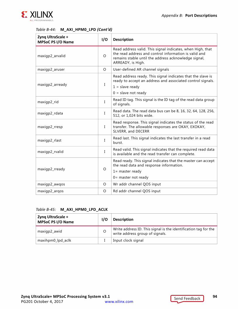
Zynq UltraScale+ MPSoC Processing System v3.1 94PG201 October 4, 2017 www.xilinx.com
Appendix B: Port Descriptions
maxigp2_arvalid O
Read address valid. This signal indicates, when High, that the read address and control information is valid and remains stable until the address acknowledge signal, ARREADY, is High.
maxigp2_aruser O User-defined AR channel signals
maxigp2_arready I
Read address ready. This signal indicates that the slave is ready to accept an address and associated control signals.
1 = slave ready
0 = slave not ready
maxigp2_rid I Read ID tag. This signal is the ID tag of the read data group of signals.
maxigp2_rdata I Read data. The read data bus can be 8, 16, 32, 64, 128, 256, 512, or 1,024 bits wide.
maxigp2_rresp IRead response. This signal indicates the status of the read transfer. The allowable responses are OKAY, EXOKAY, SLVERR, and DECERR
maxigp2_rlast I Read last. This signal indicates the last transfer in a read burst.
maxigp2_rvalid I Read valid. This signal indicates that the required read data is available and the read transfer can complete.
maxigp2_rready O
Read ready. This signal indicates that the master can accept the read data and response information.
1= master ready
0= master not ready
maxigp2_awqos O Wr addr channel QOS input
maxigp2_arqos O Rd addr channel QOS input
Table B‐45: M_AXI_HPM0_LPD_ACLK
Zynq UltraScale + MPSoC PS I/O Name
I/O Description
maxigp2_awid O Write address ID. This signal is the identification tag for the write address group of signals.
maxihpm0_lpd_aclk I Input clock signal
Table B‐44: M_AXI_HPM0_LPD (Cont’d)
Zynq UltraScale + MPSoC PS I/O Name
I/O Description
Send Feedback
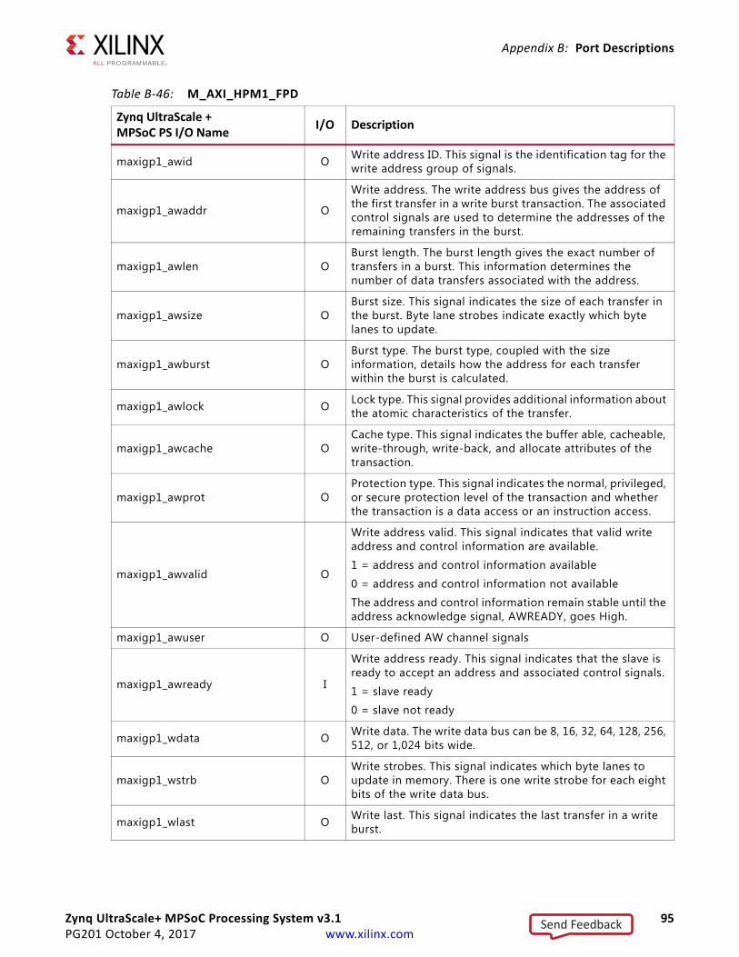
Zynq UltraScale+ MPSoC Processing System v3.1 95PG201 October 4, 2017 www.xilinx.com
Appendix B: Port Descriptions
Table B‐46: M_AXI_HPM1_FPD
Zynq UltraScale + MPSoC PS I/O Name
I/O Description
maxigp1_awid O Write address ID. This signal is the identification tag for the write address group of signals.
maxigp1_awaddr O
Write address. The write address bus gives the address of the first transfer in a write burst transaction. The associated control signals are used to determine the addresses of the remaining transfers in the burst.
maxigp1_awlen OBurst length. The burst length gives the exact number of transfers in a burst. This information determines the number of data transfers associated with the address.
maxigp1_awsize OBurst size. This signal indicates the size of each transfer in the burst. Byte lane strobes indicate exactly which byte lanes to update.
maxigp1_awburst OBurst type. The burst type, coupled with the size information, details how the address for each transfer within the burst is calculated.
maxigp1_awlock O Lock type. This signal provides additional information about the atomic characteristics of the transfer.
maxigp1_awcache OCache type. This signal indicates the buffer able, cacheable, write-through, write-back, and allocate attributes of the transaction.
maxigp1_awprot OProtection type. This signal indicates the normal, privileged, or secure protection level of the transaction and whether the transaction is a data access or an instruction access.
maxigp1_awvalid O
Write address valid. This signal indicates that valid write address and control information are available.
1 = address and control information available
0 = address and control information not available
The address and control information remain stable until the address acknowledge signal, AWREADY, goes High.
maxigp1_awuser O User-defined AW channel signals
maxigp1_awready I
Write address ready. This signal indicates that the slave is ready to accept an address and associated control signals.
1 = slave ready
0 = slave not ready
maxigp1_wdata O Write data. The write data bus can be 8, 16, 32, 64, 128, 256, 512, or 1,024 bits wide.
maxigp1_wstrb OWrite strobes. This signal indicates which byte lanes to update in memory. There is one write strobe for each eight bits of the write data bus.
maxigp1_wlast O Write last. This signal indicates the last transfer in a write burst.
Send Feedback

Zynq UltraScale+ MPSoC Processing System v3.1 96PG201 October 4, 2017 www.xilinx.com
Appendix B: Port Descriptions
maxigp1_wvalid O
Write valid. This signal indicates that valid write data and strobes are available.
1 = write data and strobes available
0 = write data and strobes not available
maxigp1_wready I
Write ready. This signal indicates that the slave can accept the write data.
1 = slave ready
0 = slave not ready
maxigp1_bid I Response ID. The identification tag of the write response
maxigp1_bresp IWrite response. This signal indicates the status of the write transaction. The allowable responses are OKAY, EXOKAY, SLVERR, and DECERR.
maxigp1_bvalid I
Write response valid. This signal indicates that a valid write response is available.
1 = write response available
0 = write response not available
maxigp1_bready O
Response ready. This signal indicates that the master can accept the response information.
1 = master ready
0 = master not ready
maxigp1_arid O Read address ID. This signal is the identification tag for the read address group of signals.
maxigp1_araddr O Read address. The read address bus gives the initial address of a read burst transaction.
maxigp1_arlen OBurst length. The burst length gives the exact number of transfers in a burst. This information determines the number of data transfers associated with the address.
maxigp1_arsize O Burst size. This signal indicates the size of each transfer in the burst.
maxigp1_arburst OBurst type. The burst type, coupled with the size information, details how the address for each transfer within the burst is calculated.
maxigp1_arlock O Lock type. This signal provides additional information about the atomic characteristics of the transfer.
maxigp1_arcache O Cache type. This signal provides additional information about the cacheable characteristics of the transfer.
maxigp1_arprot O Protection type. This signal provides protection unit information for the transaction.
Table B‐46: M_AXI_HPM1_FPD (Cont’d)
Zynq UltraScale + MPSoC PS I/O Name
I/O Description
Send Feedback

Zynq UltraScale+ MPSoC Processing System v3.1 97PG201 October 4, 2017 www.xilinx.com
Appendix B: Port Descriptions
maxigp1_arvalid O
Read address valid. This signal indicates, when High, that the read address and control information is valid and remains stable until the address acknowledge signal,
ARREADY, is High.
maxigp1_aruser O User-defined AR channel signals
maxigp1_arready I
Read address ready. This signal indicates that the slave is ready to accept an address and associated control signals.
1 = slave ready
0 = slave not ready
maxigp1_rid I Read ID tag. This signal is the ID tag of the read data group of signals.
maxigp1_rdata I Read data. The read data bus can be 8, 16, 32, 64, 128, 256, 512, or 1,024 bits wide.
maxigp1_rresp IRead response. This signal indicates the status of the read transfer. The allowable responses are OKAY, EXOKAY, SLVERR, and DECERR.
maxigp1_rlast I Read last. This signal indicates the last transfer in a read burst.
maxigp1_rvalid I Read valid. This signal indicates that the required read data is available and the read transfer can complete.
maxigp1_rready O
Read ready. This signal indicates that the master can accept the read data and response information.
1= master ready
0 = master not ready
maxigp1_awqos O Wr addr channel QOS input
maxigp1_arqos O Rd addr channel QOS input
Table B‐47: M_AXI_HPM1_FPD_ACLK
Zynq UltraScale + MPSoC PS I/O Name
I/O Description
maxigp1_awid O Write address ID. This signal is the identification tag for the write address group of signals.
maxihpm1_fpd_aclk I Input clock signal
Table B‐46: M_AXI_HPM1_FPD (Cont’d)
Zynq UltraScale + MPSoC PS I/O Name
I/O Description
Send Feedback

Zynq UltraScale+ MPSoC Processing System v3.1 98PG201 October 4, 2017 www.xilinx.com
Appendix B: Port Descriptions
Table B‐48: S_AXI_ACE_FPD
Zynq UltraScale + MPSoC PS I/O Name
I/O Description
sacefpd_wuser I User signal. Optional user-defined signal in the write data channel.
sacefpd_buser O User signal. Optional user-defined signal in the write response channel.
sacefpd_ruser O User signal. Optional user-defined signal in the read data channel.
sacefpd_awuser I User signal. Optional user-defined signal in the write address channel.
sacefpd_awsnoop I This signal indicates the transaction type for shareable write transactions.
sacefpd_awsize IBurst size. This signal indicates the size of each transfer in the burst. Byte lane strobes indicate exactly which byte lanes to update.
sacefpd_awregion I Region identifier. Permits a single physical interface on a slave to be used for multiple logical interfaces.
sacefpd_awqos I Quality of service. Identifier sent for each write transaction.
sacefpd_awprot IProtection type. This signal indicates the normal, privileged, or secure protection level of the transaction and whether the transaction is a data access or an instruction access.
sacefpd_awlen IBurst length. The burst length gives the exact number of transfers in a burst. This information determines the number of data transfers associated with the address.
sacefpd_awid I Write address ID. This signal is the identification tag for the write address group of signals.
sacefpd_awdomain I The signal indicates the shareability domain of a write transaction.
sacefpd_awcache ICache type. This signal indicates the buffer able, cacheable, write-through, write-back, and allocate attributes of the transaction.
sacefpd_awburst IBurst type. The burst type, coupled with the size information, details how the address for each transfer within the burst is calculated.
sacefpd_awbar I This signal indicates a write barrier transaction.
sacefpd_awaddr I
Write address. The write address bus gives the address of the first transfer in a write burst transaction. The associated control signals are used to determine the addresses of the
remaining transfers in the burst.
sacefpd_awlock I Lock type. This signal provides additional information about the atomic characteristics of the transfer.
Send Feedback

Zynq UltraScale+ MPSoC Processing System v3.1 99PG201 October 4, 2017 www.xilinx.com
Appendix B: Port Descriptions
sacefpd_awvalid I
Write address valid. This signal indicates that valid write address and control information are available.
1 = address and control information available
0 = address and control information not available
The address and control information remain stable until the address acknowledge signal, AWREADY, goes High.
sacefpd_awready O Write address channel ready signal
sacefpd_wstrb IWrite strobes. This signal indicates which byte lanes to update in memory. There is one write strobe for each eight bits of the write data bus.
sacefpd_wdata I Write data. The write data bus can be 8, 16, 32, 64, 128, 256, 512, or 1,024 bits wide.
sacefpd_wlast I Write last. This signal indicates the last transfer in a write burst.
sacefpd_wvalid I
Write valid. This signal indicates that valid write data and strobes are available.
1 = write data and strobes available
0 = write data and strobes not available
sacefpd_wready O
Write ready. This signal indicates that the slave can accept the write data.
1 = slave ready
0 = slave not ready
sacefpd_bresp OWrite response. This signal indicates the status of the write transaction. The allowable responses are OKAY, EXOKAY, SLVERR, and DECERR.
sacefpd_bid O Response ID. The identification tag of the write response
sacefpd_bvalid O
Write response valid. This signal indicates that a valid write response is available.
1 = write response available
0 = write response not available
sacefpd_bready I
Response ready. This signal indicates that the master can accept the response information.
1 = master ready
0 = master not ready
sacefpd_aruser I User signal. Optional User-defined signal in the read address channel.
sacefpd_arsnoop I This signal indicates the transaction type for shareable read transactions.
sacefpd_arsize I Burst size. This signal indicates the size of each transfer in the burst.
Table B‐48: S_AXI_ACE_FPD (Cont’d)
Zynq UltraScale + MPSoC PS I/O Name
I/O Description
Send Feedback
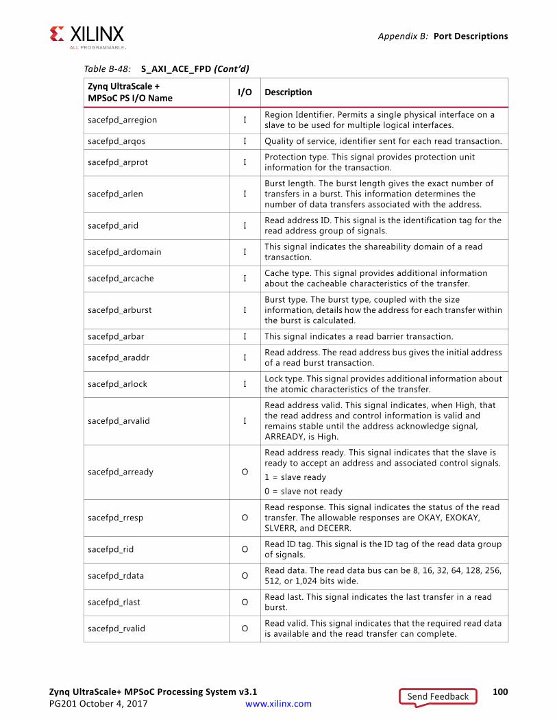
Zynq UltraScale+ MPSoC Processing System v3.1 100PG201 October 4, 2017 www.xilinx.com
Appendix B: Port Descriptions
sacefpd_arregion I Region Identifier. Permits a single physical interface on a slave to be used for multiple logical interfaces.
sacefpd_arqos I Quality of service, identifier sent for each read transaction.
sacefpd_arprot I Protection type. This signal provides protection unit information for the transaction.
sacefpd_arlen IBurst length. The burst length gives the exact number of transfers in a burst. This information determines the number of data transfers associated with the address.
sacefpd_arid I Read address ID. This signal is the identification tag for the read address group of signals.
sacefpd_ardomain I This signal indicates the shareability domain of a read transaction.
sacefpd_arcache I Cache type. This signal provides additional information about the cacheable characteristics of the transfer.
sacefpd_arburst IBurst type. The burst type, coupled with the size information, details how the address for each transfer within the burst is calculated.
sacefpd_arbar I This signal indicates a read barrier transaction.
sacefpd_araddr I Read address. The read address bus gives the initial address of a read burst transaction.
sacefpd_arlock I Lock type. This signal provides additional information about the atomic characteristics of the transfer.
sacefpd_arvalid I
Read address valid. This signal indicates, when High, that the read address and control information is valid and remains stable until the address acknowledge signal, ARREADY, is High.
sacefpd_arready O
Read address ready. This signal indicates that the slave is ready to accept an address and associated control signals.
1 = slave ready
0 = slave not ready
sacefpd_rresp ORead response. This signal indicates the status of the read transfer. The allowable responses are OKAY, EXOKAY, SLVERR, and DECERR.
sacefpd_rid O Read ID tag. This signal is the ID tag of the read data group of signals.
sacefpd_rdata O Read data. The read data bus can be 8, 16, 32, 64, 128, 256, 512, or 1,024 bits wide.
sacefpd_rlast O Read last. This signal indicates the last transfer in a read burst.
sacefpd_rvalid O Read valid. This signal indicates that the required read data is available and the read transfer can complete.
Table B‐48: S_AXI_ACE_FPD (Cont’d)
Zynq UltraScale + MPSoC PS I/O Name
I/O Description
Send Feedback
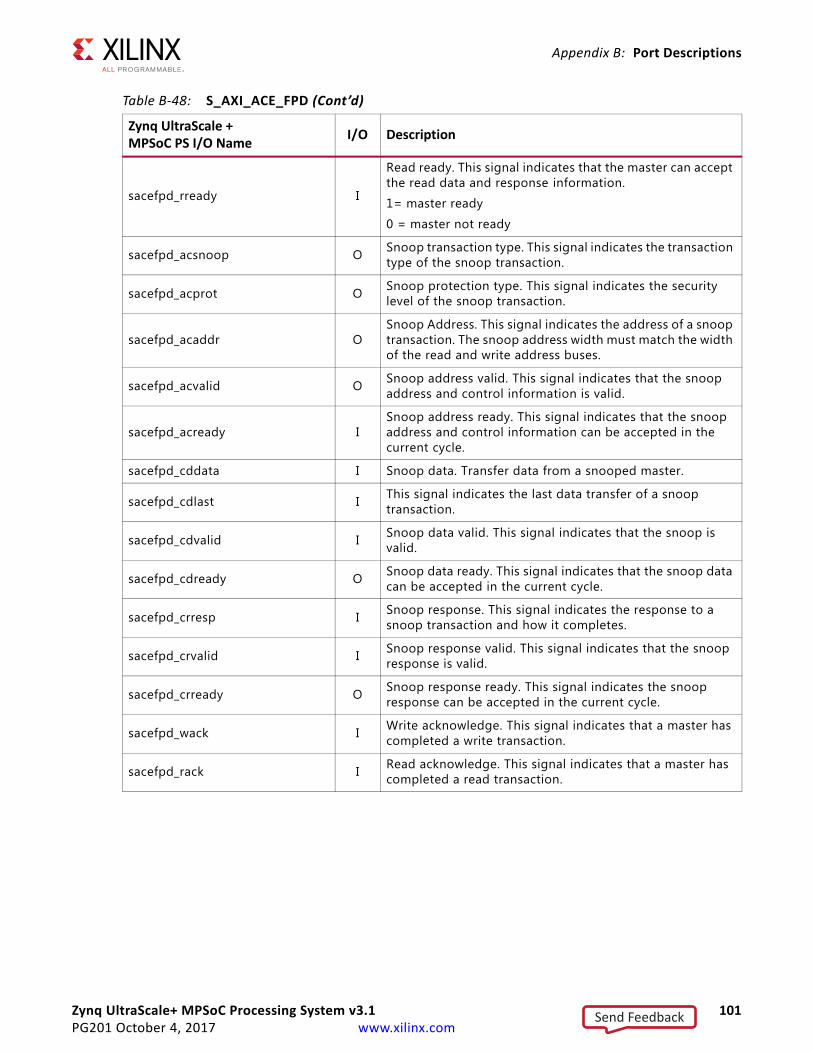
Zynq UltraScale+ MPSoC Processing System v3.1 101PG201 October 4, 2017 www.xilinx.com
Appendix B: Port Descriptions
sacefpd_rready I
Read ready. This signal indicates that the master can accept the read data and response information.
1= master ready
0 = master not ready
sacefpd_acsnoop O Snoop transaction type. This signal indicates the transaction type of the snoop transaction.
sacefpd_acprot O Snoop protection type. This signal indicates the security level of the snoop transaction.
sacefpd_acaddr OSnoop Address. This signal indicates the address of a snoop transaction. The snoop address width must match the width of the read and write address buses.
sacefpd_acvalid O Snoop address valid. This signal indicates that the snoop address and control information is valid.
sacefpd_acready ISnoop address ready. This signal indicates that the snoop address and control information can be accepted in the current cycle.
sacefpd_cddata I Snoop data. Transfer data from a snooped master.
sacefpd_cdlast I This signal indicates the last data transfer of a snoop transaction.
sacefpd_cdvalid I Snoop data valid. This signal indicates that the snoop is valid.
sacefpd_cdready O Snoop data ready. This signal indicates that the snoop data can be accepted in the current cycle.
sacefpd_crresp I Snoop response. This signal indicates the response to a snoop transaction and how it completes.
sacefpd_crvalid I Snoop response valid. This signal indicates that the snoop response is valid.
sacefpd_crready O Snoop response ready. This signal indicates the snoop response can be accepted in the current cycle.
sacefpd_wack I Write acknowledge. This signal indicates that a master has completed a write transaction.
sacefpd_rack I Read acknowledge. This signal indicates that a master has completed a read transaction.
Table B‐48: S_AXI_ACE_FPD (Cont’d)
Zynq UltraScale + MPSoC PS I/O Name
I/O Description
Send Feedback
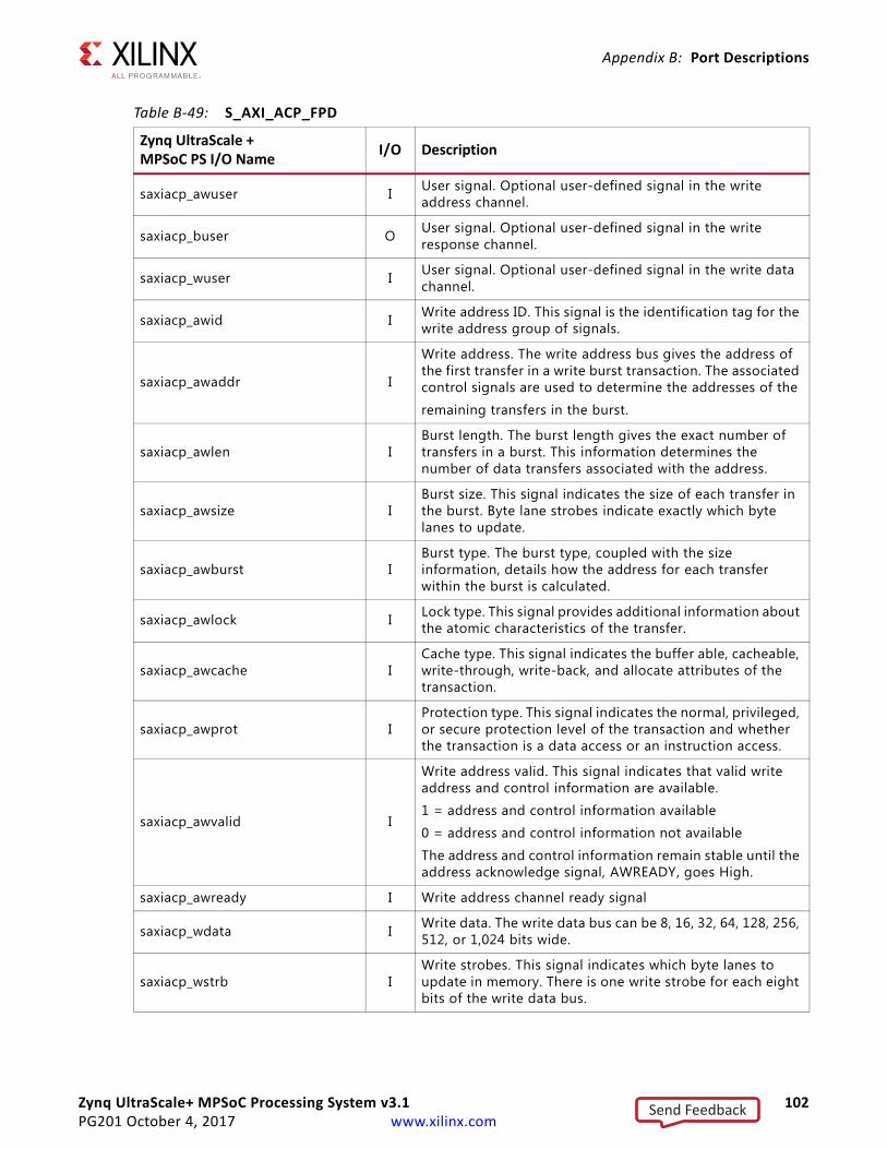
Zynq UltraScale+ MPSoC Processing System v3.1 102PG201 October 4, 2017 www.xilinx.com
Appendix B: Port Descriptions
Table B‐49: S_AXI_ACP_FPD
Zynq UltraScale + MPSoC PS I/O Name
I/O Description
saxiacp_awuser I User signal. Optional user-defined signal in the write address channel.
saxiacp_buser O User signal. Optional user-defined signal in the write response channel.
saxiacp_wuser I User signal. Optional user-defined signal in the write data channel.
saxiacp_awid I Write address ID. This signal is the identification tag for the write address group of signals.
saxiacp_awaddr I
Write address. The write address bus gives the address of the first transfer in a write burst transaction. The associated control signals are used to determine the addresses of the
remaining transfers in the burst.
saxiacp_awlen IBurst length. The burst length gives the exact number of transfers in a burst. This information determines the number of data transfers associated with the address.
saxiacp_awsize IBurst size. This signal indicates the size of each transfer in the burst. Byte lane strobes indicate exactly which byte lanes to update.
saxiacp_awburst IBurst type. The burst type, coupled with the size information, details how the address for each transfer within the burst is calculated.
saxiacp_awlock I Lock type. This signal provides additional information about the atomic characteristics of the transfer.
saxiacp_awcache ICache type. This signal indicates the buffer able, cacheable, write-through, write-back, and allocate attributes of the transaction.
saxiacp_awprot IProtection type. This signal indicates the normal, privileged, or secure protection level of the transaction and whether the transaction is a data access or an instruction access.
saxiacp_awvalid I
Write address valid. This signal indicates that valid write address and control information are available.
1 = address and control information available
0 = address and control information not available
The address and control information remain stable until the address acknowledge signal, AWREADY, goes High.
saxiacp_awready I Write address channel ready signal
saxiacp_wdata I Write data. The write data bus can be 8, 16, 32, 64, 128, 256, 512, or 1,024 bits wide.
saxiacp_wstrb IWrite strobes. This signal indicates which byte lanes to update in memory. There is one write strobe for each eight bits of the write data bus.
Send Feedback

Zynq UltraScale+ MPSoC Processing System v3.1 103PG201 October 4, 2017 www.xilinx.com
Appendix B: Port Descriptions
saxiacp_wlast I Write last. This signal indicates the last transfer in a write burst.
saxiacp_wvalid O
Write valid. This signal indicates that valid write data and strobes are available.
1 = write data and strobes available
0 = write data and strobes not available
saxiacp_wready O
Write ready. This signal indicates that the slave can accept the write data.
1 = slave ready
0 = slave not ready
saxiacp_bid O Response ID. The identification tag of the write response
saxiacp_bresp OWrite response. This signal indicates the status of the write transaction. The allowable responses are OKAY, EXOKAY, SLVERR, and DECERR.
saxiacp_bvalid I
Write response valid. This signal indicates that a valid write response is available.
1 = write response available
0 = write response not available
saxiacp_bready I
Response ready. This signal indicates that the master can accept the response information.
1 = master ready
0 = master not ready
saxiacp_arid I Read address ID. This signal is the identification tag for the read address group of signals.
saxiacp_araddr I Read address. The read address bus gives the initial address of a read burst transaction.
saxiacp_arlen IBurst length. The burst length gives the exact number of transfers in a burst. This information determines the number of data transfers associated with the address.
saxiacp_arsize I Burst size. This signal indicates the size of each transfer in the burst.
saxiacp_arburst IBurst type. The burst type and the size information determine how the address for each transfer within the burst is calculated.
saxiacp_arlock I Lock type. This signal provides additional information about the atomic characteristics of the transfer.
saxiacp_arcache I Cache type. This signal provides additional information about the cacheable characteristics of the transfer.
saxiacp_arprot IProtection type. This signal indicates the privilege and security level of the transaction, and whether the transaction is a data access or an instruction access.
Table B‐49: S_AXI_ACP_FPD (Cont’d)
Zynq UltraScale + MPSoC PS I/O Name
I/O Description
Send Feedback

Zynq UltraScale+ MPSoC Processing System v3.1 104PG201 October 4, 2017 www.xilinx.com
Appendix B: Port Descriptions
saxiacp_arvalid O
Read address valid. This signal indicates, when High, that the read address and control information is valid and remains stable until the address acknowledge signal,
ARREADY, is High
saxiacp_arready O
Read address ready. This signal indicates that the slave is ready to accept an address and associated control signals.
1 = slave ready
0 = slave not ready
saxiacp_rid O Read ID tag. This signal is the ID tag of the read data group of signals.
saxiacp_rdata O Read data. The read data bus can be 8, 16, 32, 64, 128, 256, 512, or 1,024 bits wide.
saxiacp_rresp ORead response. This signal indicates the status of the read transfer. The allowable responses are OKAY, EXOKAY, SLVERR, and DECERR.
saxiacp_rlast I Read last. This signal indicates the last transfer in a read burst.
saxiacp_rvalid O Read valid. This signal indicates that the required read data is available and the read transfer can complete.
saxiacp_rready O
Read ready. This signal indicates that the master can accept the read data and response information.
1= master ready
0 = master not ready
saxiacp_awqos O Wr addr channel QOS input.
saxiacp_arqos O Rd addr channel QOS input. Quality of service, sent for each read transaction.
Table B‐50: S_AXI_ACP_FPD_ACLK
Zynq UltraScale + MPSoC PS I/O Name
I/O Description
saxiacp_awuser I User signal. Optional user-defined signal in the write address channel
saxiacp_fpd_aclk I Input clock signal
Table B‐49: S_AXI_ACP_FPD (Cont’d)
Zynq UltraScale + MPSoC PS I/O Name
I/O Description
Send Feedback

Zynq UltraScale+ MPSoC Processing System v3.1 105PG201 October 4, 2017 www.xilinx.com
Appendix B: Port Descriptions
Table B‐51: S_AXI_HP0_FPD
Zynq UltraScale + MPSoC PS I/O Name
I/O Description
saxigp2_aruser I User-defined AR channel signals
saxigp2_awuser I User-defined AW channel signals
saxigp2_awid I Write address ID. This signal is the identification tag for the write address group of signals.
saxigp2_awaddr I
Write address. The write address bus gives the address of the first transfer in a write burst transaction. The associated control signals are used to determine the addresses of the
remaining transfers in the burst.
saxigp2_awlen IBurst length. The burst length gives the exact number of transfers in a burst. This information determines the number of data transfers associated with the address.
saxigp2_awsize IBurst size. This signal indicates the size of each transfer in the burst. Byte lane strobes indicate exactly which byte lanes to update.
saxigp2_awburst IBurst type. The burst type, coupled with the size information, details how the address for each transfer within the burst is calculated.
saxigp2_awlock I Lock type. This signal provides additional information about the atomic characteristics of the transfer.
saxigp2_awcache ICache type. This signal indicates the buffer able, cacheable, write-through, write-back, and allocate attributes of the transaction.
saxigp2_awprot IProtection type. This signal indicates the normal, privileged, or secure protection level of the transaction and whether the transaction is a data access or an instruction access.
saxigp2_awvalid I
Write address valid. This signal indicates that valid write address and control information are available.
1 = address and control information available
0 = address and control information not available.
The address and control information remain stable until the address acknowledge signal, AWREADY, goes High.
saxigp2_awready O Write address channel ready signal
saxigp2_wdata I Write data. The write data bus can be 8, 16, 32, 64, 128, 256, 512, or 1,024 bits wide
saxigp2_wstrb IWrite strobes. This signal indicates which byte lanes to update in memory. There is one write strobe for each eight bits of the write data bus.
saxigp2_wlast I Write last. This signal indicates the last transfer in a write burst.
Send Feedback
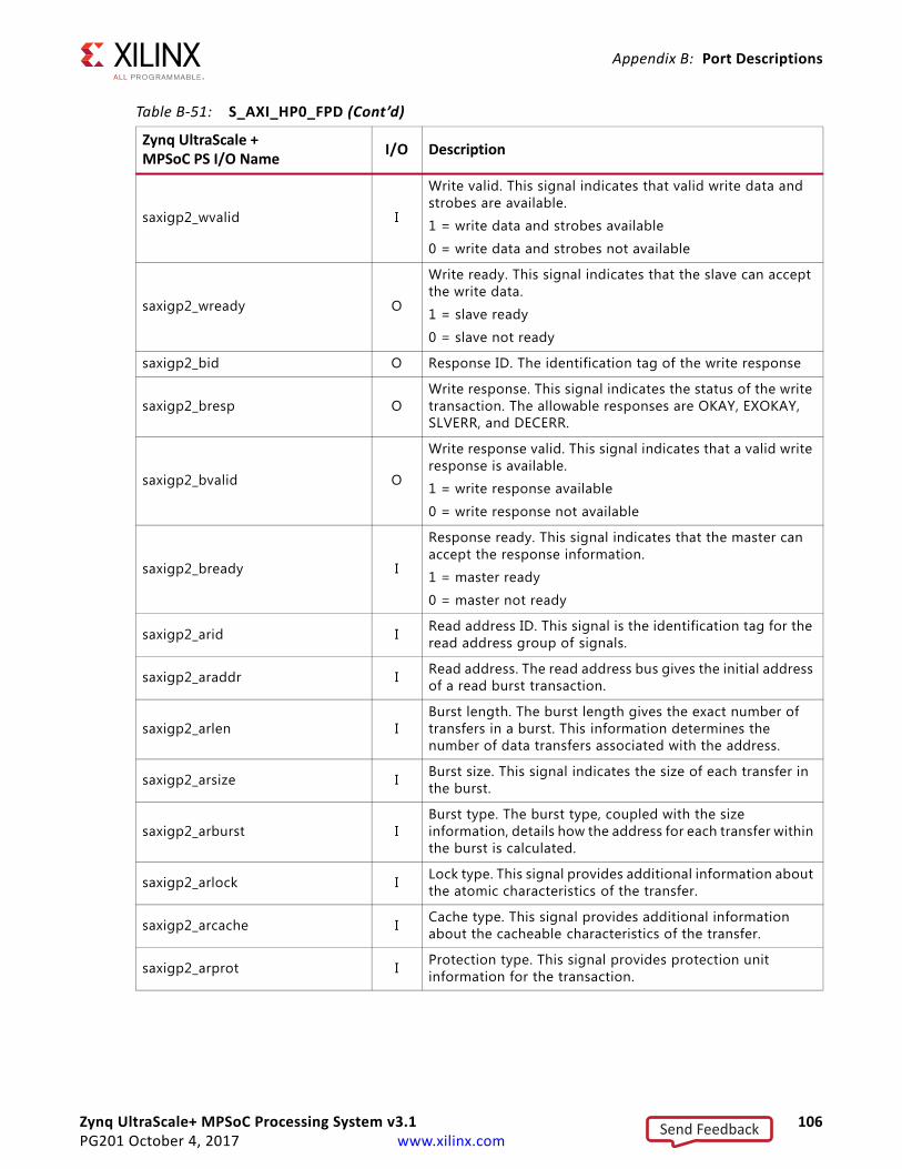
Zynq UltraScale+ MPSoC Processing System v3.1 106PG201 October 4, 2017 www.xilinx.com
Appendix B: Port Descriptions
saxigp2_wvalid I
Write valid. This signal indicates that valid write data and strobes are available.
1 = write data and strobes available
0 = write data and strobes not available
saxigp2_wready O
Write ready. This signal indicates that the slave can accept the write data.
1 = slave ready
0 = slave not ready
saxigp2_bid O Response ID. The identification tag of the write response
saxigp2_bresp OWrite response. This signal indicates the status of the write transaction. The allowable responses are OKAY, EXOKAY, SLVERR, and DECERR.
saxigp2_bvalid O
Write response valid. This signal indicates that a valid write response is available.
1 = write response available
0 = write response not available
saxigp2_bready I
Response ready. This signal indicates that the master can accept the response information.
1 = master ready
0 = master not ready
saxigp2_arid I Read address ID. This signal is the identification tag for the read address group of signals.
saxigp2_araddr I Read address. The read address bus gives the initial address of a read burst transaction.
saxigp2_arlen IBurst length. The burst length gives the exact number of transfers in a burst. This information determines the number of data transfers associated with the address.
saxigp2_arsize I Burst size. This signal indicates the size of each transfer in the burst.
saxigp2_arburst IBurst type. The burst type, coupled with the size information, details how the address for each transfer within the burst is calculated.
saxigp2_arlock I Lock type. This signal provides additional information about the atomic characteristics of the transfer.
saxigp2_arcache I Cache type. This signal provides additional information about the cacheable characteristics of the transfer.
saxigp2_arprot I Protection type. This signal provides protection unit information for the transaction.
Table B‐51: S_AXI_HP0_FPD (Cont’d)
Zynq UltraScale + MPSoC PS I/O Name
I/O Description
Send Feedback

Zynq UltraScale+ MPSoC Processing System v3.1 107PG201 October 4, 2017 www.xilinx.com
Appendix B: Port Descriptions
saxigp2_arvalid I
Read address valid. This signal indicates, when High, that the read address and control information is valid and remains stable until the address acknowledge signal,
ARREADY, is High.
saxigp2_arready O
Read address ready. This signal indicates that the slave is ready to accept an address and associated control signals.
1 = slave ready
0 = slave not ready
saxigp2_rid O Read ID tag. This signal is the ID tag of the read data group of signals.
saxigp2_rdata O Read data. The read data bus can be 8, 16, 32, 64, 128, 256, 512, or 1,024 bits wide.
saxigp2_rresp ORead response. This signal indicates the status of the read transfer. The allowable responses are OKAY, EXOKAY, SLVERR, and DECERR.
saxigp2_rlast O Read last. This signal indicates the last transfer in a read burst.
saxigp2_rvalid O Read valid. This signal indicates that the required read data is available and the read transfer can complete.
saxigp2_rready I
Read ready. This signal indicates that the master can accept the read data and response information.
1= master ready
0 = master not ready
saxigp2_awqos O Wr addr channel QOS input
saxigp2_arqos O Rd addr channel QOS input
saxigp2_rcount O Rd data channel fill level
saxigp2_wcount O Wr data channel fill level
saxigp2_racount O Rd addr channel fill level
saxigp2_wacount O Wr addr channel fill level
Table B‐52: S_AXI_HP0_FPD_ACLK
Zynq UltraScale + MPSoC PS I/O Name
I/O Description
saxigp2_aruser I User-defined AR channel signals
saxihp0_fpd_aclk I Input clock signal
Table B‐51: S_AXI_HP0_FPD (Cont’d)
Zynq UltraScale + MPSoC PS I/O Name
I/O Description
Send Feedback

Zynq UltraScale+ MPSoC Processing System v3.1 108PG201 October 4, 2017 www.xilinx.com
Appendix B: Port Descriptions
Table B‐53: S_AXI_HP0_FPD_RCLK
Zynq UltraScale + MPSoC PS I/O Name
I/O Description
saxigp2_aruser I User-defined AR channel signals
saxihp0_fpd_rclk I Read clock signal
Table B‐54: S_AXI_HP0_FPD_WCLK
Zynq UltraScale + MPSoC PS I/O Name
I/O Description
saxigp2_aruser I User-defined AR channel signals0
saxihp0_fpd_wclk I Write clock signal
Table B‐55: S_AXI_HP1_FPD
Zynq UltraScale + MPSoC PS I/O Name
I/O Description
saxigp3_aruser I User-defined AR channel signals
saxigp3_awuser I User-defined AW channel signals
saxigp3_awid I Write address ID. This signal is the identification tag for the write address group of signals.
saxigp3_awaddr I
Write address. The write address bus gives the address of the first transfer in a write burst transaction. The associated control signals are used to determine the addresses of the
remaining transfers in the burst.
saxigp3_awlen IBurst length. The burst length gives the exact number of transfers in a burst. This information determines the number of data transfers associated with the address.
saxigp3_awsize IBurst size. This signal indicates the size of each transfer in the burst. Byte lane strobes indicate exactly which byte lanes to update.
saxigp3_awburst IBurst type. The burst type, coupled with the size information, details how the address for each transfer within the burst is calculated.
saxigp3_awlock I Lock type. This signal provides additional information about the atomic characteristics of the transfer.
saxigp3_awcache ICache type. This signal indicates the buffer able, cacheable, write-through, write-back, and allocate attributes of the transaction.
saxigp3_awprot IProtection type. This signal indicates the normal, privileged, or secure protection level of the transaction and whether the transaction is a data access or an instruction access.
Send Feedback

Zynq UltraScale+ MPSoC Processing System v3.1 109PG201 October 4, 2017 www.xilinx.com
Appendix B: Port Descriptions
saxigp3_awvalid I
Write address valid. This signal indicates that valid write address and control information are available.
1 = address and control information available
0 = address and control information not available
The address and control information remain stable until the address acknowledge signal, AWREADY, goes High.
saxigp3_awready O Write address channel ready signal
saxigp3_wdata I Write data. The write data bus can be 8, 16, 32, 64, 128, 256, 512, or 1,024 bits wide.
saxigp3_wstrb IWrite strobes. This signal indicates which byte lanes to update in memory. There is one write strobe for each eight bits of the write data bus.
saxigp3_wlast I Write last. This signal indicates the last transfer in a write burst.
saxigp3_wvalid I
Write valid. This signal indicates that valid write data and strobes are available.
1 = write data and strobes available
0 = write data and strobes not available
saxigp3_wready O
Write ready. This signal indicates that the slave can accept the write data.
1 = slave ready
0 = slave not ready
saxigp3_bid O Response ID. The identification tag of the write response
saxigp3_bresp OWrite response. This signal indicates the status of the write transaction. The allowable responses are OKAY, EXOKAY, SLVERR, and DECERR.
saxigp3_bvalid O
Write response valid. This signal indicates that a valid write response is available.
1 = write response available
0 = write response not available
saxigp3_bready I
Response ready. This signal indicates that the master can accept the response information.
1 = master ready
0 = master not ready
saxigp3_arid I Read address ID. This signal is the identification tag for the read address group of signals.
saxigp3_araddr I Read address. The read address bus gives the initial address of a read burst transaction.
saxigp3_arlen IBurst length. The burst length gives the exact number of transfers in a burst. This information determines the number of data transfers associated with the address.
Table B‐55: S_AXI_HP1_FPD (Cont’d)
Zynq UltraScale + MPSoC PS I/O Name
I/O Description
Send Feedback

Zynq UltraScale+ MPSoC Processing System v3.1 110PG201 October 4, 2017 www.xilinx.com
Appendix B: Port Descriptions
saxigp3_arsize I Burst size. This signal indicates the size of each transfer in the burst
saxigp3_arburst IBurst type. The burst type, coupled with the size information, details how the address for each transfer within the burst is calculated.
saxigp3_arlock I Lock type. This signal provides additional information about the atomic characteristics of the transfer.
saxigp3_arcache I Cache type. This signal provides additional information about the cacheable characteristics of the transfer.
saxigp3_arprot I Protection type. This signal provides protection unit information for the transaction.
saxigp3_arvalid I
Read address valid. This signal indicates, when High, that the read address and control information is valid and remains stable until the address acknowledge signal,
ARREADY, is High.
saxigp3_arready O
Read address ready. This signal indicates that the slave is ready to accept an address and associated control signals.
1 = slave ready
0 = slave not ready
saxigp3_rid O Read ID tag. This signal is the ID tag of the read data group of signals.
saxigp3_rdata O Read data. The read data bus can be 8, 16, 32, 64, 128, 256, 512, or 1,024 bits wide.
saxigp3_rresp ORead response. This signal indicates the status of the read transfer. The allowable responses are OKAY, EXOKAY, SLVERR, and DECERR.
saxigp3_rlast O Read last. This signal indicates the last transfer in a read burst.
saxigp3_rvalid O Read valid. This signal indicates that the required read data is available and the read transfer can complete.
saxigp3_rready I
Read ready. This signal indicates that the master can accept the read data and response information.
1= master ready
0 = master not ready
saxigp3_awqos O Wr addr channel QOS input
saxigp3_arqos O Rd addr channel QOS input
saxigp3_rcount O Rd data channel fill level
saxigp3_wcount O Wr data channel fill level
saxigp3_racount O Rd addr channel fill level
saxigp3_wacount O Wr addr channel fill level
Table B‐55: S_AXI_HP1_FPD (Cont’d)
Zynq UltraScale + MPSoC PS I/O Name
I/O Description
Send Feedback
Zynq UltraScale+ MPSoC Processing System v3.1 111PG201 October 4, 2017 www.xilinx.com
Appendix B: Port Descriptions
Table B‐56: S_AXI_HP1_FPD_ACLK
Zynq UltraScale + MPSoC PS I/O Name
I/O Description
saxigp3_aruser I User-defined AR channel signals
Saxihp1_fpd_aclk I Input clock signal
Table B‐57: S_AXI_HP1_FPD_RCLK
Zynq UltraScale + MPSoC PS I/O Name
I/O Description
saxigp3_aruser I User-defined AR channel signals
Saxihp1_fpd_rclk I Read clock signal
Table B‐58: S_AXI_HP1_FPD_WCLK
Zynq UltraScale + MPSoC PS I/O Name
I/O Description
saxigp3_aruser I User-defined AR channel signals
saxihp1_fpd_wclk I Write clock signal
Table B‐59: S_AXI_HP2_FPD
Zynq UltraScale + MPSoC PS I/O Name
I/O Description
saxigp4_aruser I User-defined AR channel signals
saxigp4_awuser I User-defined AW channel signals
saxigp4_awid I Write address ID. This signal is the identification tag for the write address group of signals.
saxigp4_awaddr I
Write address. The write address bus gives the address of the first transfer in a write burst transaction. The associated control signals are used to determine the addresses of the
remaining transfers in the burst.
saxigp4_awlen IBurst length. The burst length gives the exact number of transfers in a burst. This information determines the number of data transfers associated with the address.
saxigp4_awsize IBurst size. This signal indicates the size of each transfer in the burst. Byte lane strobes indicate exactly which byte lanes to update.
saxigp4_awburst IBurst type. The burst type, coupled with the size information, details how the address for each transfer within the burst is calculated.
Send Feedback
Zynq UltraScale+ MPSoC Processing System v3.1 112PG201 October 4, 2017 www.xilinx.com
Appendix B: Port Descriptions
saxigp4_awlock I Lock type. This signal provides additional information about the atomic characteristics of the transfer.
saxigp4_awcache ICache type. This signal indicates the buffer able, cacheable, write-through, write-back, and allocate attributes of the transaction.
saxigp4_awprot IProtection type. This signal indicates the normal, privileged, or secure protection level of the transaction and whether the transaction is a data access or an instruction access.
saxigp4_awvalid I
Write address valid. This signal indicates that valid write address and control information are available.
1 = address and control information available
0 = address and control information not available
The address and control information remain stable until the address acknowledge signal, AWREADY, goes High.
saxigp4_awready O Write address channel ready signal
saxigp4_wdata I Write data. The write data bus can be 8, 16, 32, 64, 128, 256, 512, or 1,024 bits wide.
saxigp4_wstrb IWrite strobes. This signal indicates which byte lanes to update in memory. There is one write strobe for each eight bits of the write data bus.
saxigp4_wlast I Write last. This signal indicates the last transfer in a write burst.
saxigp4_wvalid I
Write valid. This signal indicates that valid write data and strobes are available.
1 = write data and strobes available
0 = write data and strobes not available
saxigp4_wready O
Write ready. This signal indicates that the slave can accept the write data.
1 = slave ready
0 = slave not ready
saxigp4_bid O Response ID. The identification tag of the write response
saxigp4_bresp OWrite response. This signal indicates the status of the write transaction. The allowable responses are OKAY, EXOKAY, SLVERR, and DECERR.
saxigp4_bvalid O
Write response valid. This signal indicates that a valid write response is available.
1 = write response available
0 = write response not available
Table B‐59: S_AXI_HP2_FPD (Cont’d)
Zynq UltraScale + MPSoC PS I/O Name
I/O Description
Send Feedback

Zynq UltraScale+ MPSoC Processing System v3.1 113PG201 October 4, 2017 www.xilinx.com
Appendix B: Port Descriptions
saxigp4_bready I
Response ready. This signal indicates that the master can accept the response information.
1 = master ready
0 = master not ready
saxigp4_arid I Read address ID. This signal is the identification tag for the read address group of signals.
saxigp4_araddr I Read address. The read address bus gives the initial address of a read burst transaction.
saxigp4_arlen IBurst length. The burst length gives the exact number of transfers in a burst. This information determines the number of data transfers associated with the address.
saxigp4_arsize I Burst size. This signal indicates the size of each transfer in the burst.
saxigp4_arburst IBurst type. The burst type, coupled with the size information, details how the address for each transfer within the burst is calculated.
saxigp4_arlock I Lock type. This signal provides additional information about the atomic characteristics of the transfer.
saxigp4_arcache I Cache type. This signal provides additional information about the cacheable characteristics of the transfer.
saxigp4_arprot I Protection type. This signal provides protection unit information for the transaction.
saxigp4_arvalid I
Read address valid. This signal indicates, when High, that the read address and control information is valid and remains stable until the address acknowledge signal,
ARREADY, is High.
saxigp4_arready O
Read address ready. This signal indicates that the slave is ready to accept an address and associated control signals.
1 = slave ready
0 = slave not ready
saxigp4_rid O Read ID tag. This signal is the ID tag of the read data group of signals.
saxigp4_rdata O Read data. The read data bus can be 8, 16, 32, 64, 128, 256, 512, or 1,024 bits wide.
saxigp4_rresp ORead response. This signal indicates the status of the read transfer. The allowable responses are OKAY, EXOKAY, SLVERR, and DECERR.
saxigp4_rlast O Read last. This signal indicates the last transfer in a read burst.
saxigp4_rvalid O Read valid. This signal indicates that the required read data is available and the read transfer can complete.
Table B‐59: S_AXI_HP2_FPD (Cont’d)
Zynq UltraScale + MPSoC PS I/O Name
I/O Description
Send Feedback

Zynq UltraScale+ MPSoC Processing System v3.1 114PG201 October 4, 2017 www.xilinx.com
Appendix B: Port Descriptions
saxigp4_rready I
Read ready. This signal indicates that the master can accept the read data and response information.
1= master ready
0 = master not ready
saxigp4_awqos O Wr addr channel QOS input
saxigp4_arqos O Rd addr channel QOS input
saxigp4_rcount O Rd data channel fill level
saxigp4_wcount O Wr data channel fill level
saxigp4_racount O Rd addr channel fill level
saxigp4_wacount O Wr addr channel fill level
Table B‐60: S_AXI_HP2_FPD_ACLK
Zynq UltraScale + MPSoC PS I/O Name
I/O Description
saxigp4_aruser I User-defined AR channel signals
Saxihp2_fpd_aclk I Input clock signal
Table B‐61: S_AXI_HP2_FPD_RCLK
Zynq UltraScale + MPSoC PS I/O Name
I/O Description
saxigp4_aruser I User-defined AR channel signals
Saxihp2_fpd_rclk I Read clock signal
Table B‐62: S_AXI_HP2_FPD_WCLK
Zynq UltraScale + MPSoC PS I/O Name
I/O Description
saxigp4_aruser I User-defined AR channel signals
Saxihp2_fpd_wclk I Write clock signal
Table B‐59: S_AXI_HP2_FPD (Cont’d)
Zynq UltraScale + MPSoC PS I/O Name
I/O Description
Send Feedback
Zynq UltraScale+ MPSoC Processing System v3.1 115PG201 October 4, 2017 www.xilinx.com
Appendix B: Port Descriptions
Table B‐63: S_AXI_HP3_FPD
Zynq UltraScale + MPSoC PS I/O Name
I/O Description
saxigp5_aruser I User-defined AR channel signals
saxigp5_awuser I User-defined AW channel signals
saxigp5_awid I Write address ID. This signal is the identification tag for the write address group of signals.
saxigp5_awaddr I
Write address. The write address bus gives the address of the first transfer in a write burst transaction. The associated control signals are used to determine the addresses of the
remaining transfers in the burst.
saxigp5_awlen IBurst length. The burst length gives the exact number of transfers in a burst. This information determines the number of data transfers associated with the address.
saxigp5_awsize IBurst size. This signal indicates the size of each transfer in the burst. Byte lane strobes indicate exactly which byte lanes to update.
saxigp5_awburst IBurst type. The burst type, coupled with the size information, details how the address for each transfer within the burst is calculated.
saxigp5_awlock I Lock type. This signal provides additional information about the atomic characteristics of the transfer.
saxigp5_awcache ICache type. This signal indicates the buffer able, cacheable, write-through, write-back, and allocate attributes of the transaction.
saxigp5_awprot I
Protection type. This signal indicates the normal, privileged, or secure protection level of the transaction and whether the transaction is a data access or an instruction access.
saxigp5_awvalid I
Write address valid. This signal indicates that valid write address and control information are available.
1 = address and control information available
0 = address and control information not available
The address and control information remain stable until the address acknowledge signal, AWREADY, goes High.
saxigp5_awready O Write address channel ready signal
saxigp5_wdata I Write data. The write data bus can be 8, 16, 32, 64, 128, 256, 512, or 1,024 bits wide.
saxigp5_wstrb IWrite strobes. This signal indicates which byte lanes to update in memory. There is one write strobe for each eight bits of the write data bus.
saxigp5_wlast I Write last. This signal indicates the last transfer in a write burst.
Send Feedback

Zynq UltraScale+ MPSoC Processing System v3.1 116PG201 October 4, 2017 www.xilinx.com
Appendix B: Port Descriptions
saxigp5_wvalid I
Write valid. This signal indicates that valid write data and strobes are available.
1 = write data and strobes available
0 = write data and strobes not available
saxigp5_wready O
Write ready. This signal indicates that the slave can accept the write data.
1 = slave ready
0 = slave not ready
saxigp5_bid O Response ID. The identification tag of the write response
saxigp5_bresp OWrite response. This signal indicates the status of the write transaction. The allowable responses are OKAY, EXOKAY, SLVERR, and DECERR.
saxigp5_bvalid O
Write response valid. This signal indicates that a valid write response is available.
1 = write response available
0 = write response not available
saxigp5_bready I
Response ready. This signal indicates that the master can accept the response information.
1 = master ready
0 = master not ready
saxigp5_arid I Read address ID. This signal is the identification tag for the read address group of signals.
saxigp5_araddr I Read address. The read address bus gives the initial address of a read burst transaction.
saxigp5_arlen IBurst length. The burst length gives the exact number of transfers in a burst. This information determines the number of data transfers associated with the address.
saxigp5_arsize I Burst size. This signal indicates the size of each transfer in the burst.
saxigp5_arburst IBurst type. The burst type, coupled with the size information, details how the address for each transfer within the burst is calculated.
saxigp5_arlock I Lock type. This signal provides additional information about the atomic characteristics of the transfer.
saxigp5_arcache I Cache type. This signal provides additional information about the cacheable characteristics of the transfer.
saxigp5_arprot I Protection type. This signal provides protection unit information for the transaction.
Table B‐63: S_AXI_HP3_FPD (Cont’d)
Zynq UltraScale + MPSoC PS I/O Name
I/O Description
Send Feedback
Zynq UltraScale+ MPSoC Processing System v3.1 117PG201 October 4, 2017 www.xilinx.com
Appendix B: Port Descriptions
saxigp5_arvalid I
Read address valid. This signal indicates, when High, that the read address and control information is valid and remains stable until the address acknowledge signal,
ARREADY, is High.
saxigp5_arready O
Read address ready. This signal indicates that the slave is ready to accept an address and associated control signals.
1 = slave ready
0 = slave not ready
saxigp5_rid O Read ID tag. This signal is the ID tag of the read data group of signals.
saxigp5_rdata O Read data. The read data bus can be 8, 16, 32, 64, 128, 256, 512, or 1,024 bits wide.
saxigp5_rresp ORead response. This signal indicates the status of the read transfer. The allowable responses are OKAY, EXOKAY, SLVERR, and DECERR.
saxigp5_rlast O Read last. This signal indicates the last transfer in a read burst.
saxigp5_rvalid O Read valid. This signal indicates that the required read data is available and the read transfer can complete.
saxigp5_rready I
Read ready. This signal indicates that the master can accept the read data and response information.
1= master ready
0 = master not ready
saxigp5_awqos O Wr addr channel QOS input
saxigp5_arqos O Rd addr channel QOS input
saxigp5_rcount O Rd data channel fill level
saxigp5_wcount O Wr data channel fill level
saxigp5_racount O Rd addr channel fill level
saxigp5_wacount O Wr addr channel fill level
Table B‐64: S_AXI_HP3_FPD_ACLK
Zynq UltraScale + MPSoC PS I/O Name
I/O Description
saxigp5_aruser I User-defined AR channel signals
Saxihp3_fpd_aclk I Input clock signal
Table B‐63: S_AXI_HP3_FPD (Cont’d)
Zynq UltraScale + MPSoC PS I/O Name
I/O Description
Send Feedback

Zynq UltraScale+ MPSoC Processing System v3.1 118PG201 October 4, 2017 www.xilinx.com
Appendix B: Port Descriptions
Table B‐65: S_AXI_HP3_FPD_RCLK
Zynq UltraScale + MPSoC PS I/O Name
I/O Description
saxigp5_aruser I User-defined AR channel signals
Saxihp3_fpd_rclk I Read clock signal
Table B‐66: S_AXI_HP1_FPD_WCLK
Zynq UltraScale + MPSoC PS I/O Name
I/O Description
saxigp5_aruser I User-defined AR channel signals
Saxihp3_fpd_wclk I Write clock signal
Table B‐67: S_AXI_HPC0_FPD
Zynq UltraScale + MPSoC PS I/O Name
I/O Description
saxigp0_aruser I User-defined AR channel signals
saxigp0_awuser I User-defined AW channel signals
saxigp0_awid I Write address ID. This signal is the identification tag for the write address group of signals.
saxigp0_awaddr I
Write address. The write address bus gives the address of the first transfer in a write burst transaction. The associated control signals are used to determine the addresses of the
remaining transfers in the burst.
saxigp0_awlen IBurst length. The burst length gives the exact number of transfers in a burst. This information determines the number of data transfers associated with the address.
saxigp0_awsize IBurst size. This signal indicates the size of each transfer in the burst. Byte lane strobes indicate exactly which byte lanes to update.
saxigp0_awburst IBurst type. The burst type, coupled with the size information, details how the address for each transfer within the burst is calculated.
saxigp0_awlock I Lock type. This signal provides additional information about the atomic characteristics of the transfer.
saxigp0_awcache ICache type. This signal indicates the buffer able, cacheable, write-through, write-back, and allocate attributes of the transaction.
saxigp0_awprot I
Protection type. This signal indicates the normal, privileged, or secure protection level of the transaction and whether the transaction is a data access or an instruction access.
Send Feedback
Zynq UltraScale+ MPSoC Processing System v3.1 119PG201 October 4, 2017 www.xilinx.com
Appendix B: Port Descriptions
saxigp0_awvalid I
Write address valid. This signal indicates that valid write address and control information are available.
1 = address and control information available
0 = address and control information not available
The address and control information remain stable until the address acknowledge signal, AWREADY, goes High.
saxigp0_awready O Write address channel ready signal
saxigp0_wdata I Write data. The write data bus can be 8, 16, 32, 64, 128, 256, 512, or 1,024 bits wide.
saxigp0_wstrb IWrite strobes. This signal indicates which byte lanes to update in memory. There is one write strobe for each eight bits of the write data bus.
saxigp0_wlast I Write last. This signal indicates the last transfer in a write burst.
saxigp0_wvalid I
Write valid. This signal indicates that valid write data and strobes are available.
1 = write data and strobes available
0 = write data and strobes not available
saxigp0_wready O
Write ready. This signal indicates that the slave can accept the write data.
1 = slave ready
0 = slave not ready
saxigp0_bid O Response ID. The identification tag of the write response
saxigp0_bresp OWrite response. This signal indicates the status of the write transaction. The allowable responses are OKAY, EXOKAY, SLVERR, and DECERR.
saxigp0_bvalid O
Write response valid. This signal indicates that a valid write response is available.
1 = write response available
0 = write response not available
saxigp0_bready I
Response ready. This signal indicates that the master can accept the response information.
1 = master ready
0 = master not ready
saxigp0_arid I Read address ID. This signal is the identification tag for the read address group of signals.
saxigp0_araddr I Read address. The read address bus gives the initial address of a read burst transaction.
saxigp0_arlen IBurst length. The burst length gives the exact number of transfers in a burst. This information determines the number of data transfers associated with the address.
Table B‐67: S_AXI_HPC0_FPD (Cont’d)
Zynq UltraScale + MPSoC PS I/O Name
I/O Description
Send Feedback

Zynq UltraScale+ MPSoC Processing System v3.1 120PG201 October 4, 2017 www.xilinx.com
Appendix B: Port Descriptions
saxigp0_arsize I Burst size. This signal indicates the size of each transfer in the burst.
saxigp0_arburst IBurst type. The burst type, coupled with the size information, details how the address for each transfer within the burst is calculated.
saxigp0_arlock I Lock type. This signal provides additional information about the atomic characteristics of the transfer.
saxigp0_arcache I Cache type. This signal provides additional information about the cacheable characteristics of the transfer.
saxigp0_arprot I Protection type. This signal provides protection unit information for the transaction.
saxigp0_arvalid I
Read address valid. This signal indicates, when High, that the read address and control information is valid and remains stable until the address acknowledge signal,
ARREADY, is High.
saxigp0_arready O
Read address ready. This signal indicates that the slave is ready to accept an address and associated control signals.
1 = slave ready
0 = slave not ready.
saxigp0_rid O Read ID tag. This signal is the ID tag of the read data group of signals.
saxigp0_rdata O Read data. The read data bus can be 8, 16, 32, 64, 128, 256, 512, or 1,024 bits wide.
saxigp0_rresp ORead response. This signal indicates the status of the read transfer. The allowable responses are OKAY, EXOKAY, SLVERR, and DECERR.
saxigp0_rlast O Read last. This signal indicates the last transfer in a read burst.
saxigp0_rvalid O Read valid. This signal indicates that the required read data is available and the read transfer can complete.
saxigp0_rready I
Read ready. This signal indicates that the master can accept the read data and response information.
1= master ready
0 = master not ready
saxigp0_awqos O Wr addr channel QOS input
saxigp0_arqos O Rd addr channel QOS input
saxigp0_rcount O Rd data channel fill level
saxigp0_wcount O Wr data channel fill level
saxigp0_racount O Rd addr channel fill level
saxigp0_wacount O Wr addr channel fill level
Table B‐67: S_AXI_HPC0_FPD (Cont’d)
Zynq UltraScale + MPSoC PS I/O Name
I/O Description
Send Feedback

Zynq UltraScale+ MPSoC Processing System v3.1 121PG201 October 4, 2017 www.xilinx.com
Appendix B: Port Descriptions
Table B‐68: S_AXI_HPC0_FPD_ACLK
Zynq UltraScale + MPSoC PS I/O Name
I/O Description
saxigp0_aruser I User-defined AR channel signals
saxihpc0_fpd_aclk I Input clock signal
Table B‐69: S_AXI_HPC0_FPD_RCLK
Zynq UltraScale + MPSoC PS I/O Name
I/O Description
saxigp0_aruser I User-defined AR channel signals
saxihpc0_fpd_rclk I Read clock signal
Table B‐70: S_AXI_HPC0_FPD_WCLK
Zynq UltraScale + MPSoC PS I/O Name
I/O Description
saxigp0_aruser I User-defined AR channel signals
saxihpc0_fpd_wclk I Write clock signal
Table B‐71: S_AXI_HPC1_FPD
Zynq UltraScale + MPSoC PS I/O Name
I/O Description
Saxigp1_aruser I User-defined AR channel signals
Saxigp1_awuser I User-defined AW channel signals
Saxigp1_awid I Write address ID. This signal is the identification tag for the write address group of signals.
Saxigp1_awaddr I
Write address. The write address bus gives the address of the first transfer in a write burst transaction. The associated control signals are used to determine the addresses of the
remaining transfers in the burst.
Saxigp1_awlen IBurst length. The burst length gives the exact number of transfers in a burst. This information determines the number of data transfers associated with the address.
Saxigp1_awsize IBurst size. This signal indicates the size of each transfer in the burst. Byte lane strobes indicate exactly which byte lanes to update.
Saxigp1_awburst IBurst type. The burst type, coupled with the size information, details how the address for each transfer within the burst is calculated.
Send Feedback

Zynq UltraScale+ MPSoC Processing System v3.1 122PG201 October 4, 2017 www.xilinx.com
Appendix B: Port Descriptions
Saxigp1_awlock I Lock type. This signal provides additional information about the atomic characteristics of the transfer.
Saxigp1_awcache ICache type. This signal indicates the buffer able, cacheable, write-through, write-back, and allocate attributes of the transaction.
Saxigp1_awprot IProtection type. This signal indicates the normal, privileged, or secure protection level of the transaction and whether the transaction is a data access or an instruction access.
Saxigp1_awvalid I
Write address valid. This signal indicates that valid write address and control information are available.
1 = address and control information available
0 = address and control information not available
The address and control information remain stable until the address acknowledge signal, AWREADY, goes High.
Saxigp1_awready O Write address channel ready signal
Saxigp1_wdata I Write data. The write data bus can be 8, 16, 32, 64, 128, 256, 512, or 1,024 bits wide.
Saxigp1_wstrb IWrite strobes. This signal indicates which byte lanes to update in memory. There is one write strobe for each eight bits of the write data bus.
Saxigp1_wlast I Write last. This signal indicates the last transfer in a write burst.
Saxigp1_wvalid I
Write valid. This signal indicates that valid write data and strobes are available.
1 = write data and strobes available
0 = write data and strobes not available
Saxigp1_wready O
Write ready. This signal indicates that the slave can accept the write data.
1 = slave ready
0 = slave not ready
Saxigp1_bid O Response ID. The identification tag of the write response
Saxigp1_bresp OWrite response. This signal indicates the status of the write transaction. The allowable responses are OKAY, EXOKAY, SLVERR, and DECERR.
Saxigp1_bvalid O
Write response valid. This signal indicates that a valid write response is available.
1 = write response available
0 = write response not available
Table B‐71: S_AXI_HPC1_FPD (Cont’d)
Zynq UltraScale + MPSoC PS I/O Name
I/O Description
Send Feedback

Zynq UltraScale+ MPSoC Processing System v3.1 123PG201 October 4, 2017 www.xilinx.com
Appendix B: Port Descriptions
Saxigp1_bready I
Response ready. This signal indicates that the master can accept the response information.
1 = master ready
0 = master not ready
Saxigp1_arid I Read address ID. This signal is the identification tag for the read address group of signals.
Saxigp1_araddr I Read address. The read address bus gives the initial address of a read burst transaction.
Saxigp1_arlen IBurst length. The burst length gives the exact number of transfers in a burst. This information determines the number of data transfers associated with the address.
Saxigp1_arsize I Burst size. This signal indicates the size of each transfer in the burst.
Saxigp1_arburst IBurst type. The burst type, coupled with the size information, details how the address for each transfer within the burst is calculated.
Saxigp1_arlock I Lock type. This signal provides additional information about the atomic characteristics of the transfer.
Saxigp1_arcache I Cache type. This signal provides additional information about the cacheable characteristics of the transfer.
Saxigp1_arprot I Protection type. This signal provides protection unit information for the transaction.
Saxigp1_arvalid I
Read address valid. This signal indicates, when High, that the read address and control information is valid and remains stable until the address acknowledge signal,
ARREADY, is High.
Saxigp1_arready O
Read address ready. This signal indicates that the slave is ready to accept an address and associated control signals.
1 = slave ready
0 = slave not ready
Saxigp1_rid O Read ID tag. This signal is the ID tag of the read data group of signals.
Saxigp1_rdata O Read data. The read data bus can be 8, 16, 32, 64, 128, 256, 512, or 1,024 bits wide.
Saxigp1_rresp ORead response. This signal indicates the status of the read transfer. The allowable responses are OKAY, EXOKAY, SLVERR, and DECERR.
Saxigp1_rlast O Read last. This signal indicates the last transfer in a read burst.
Saxigp1_rvalid O Read valid. This signal indicates that the required read data is available and the read transfer can complete.
Table B‐71: S_AXI_HPC1_FPD (Cont’d)
Zynq UltraScale + MPSoC PS I/O Name
I/O Description
Send Feedback
Zynq UltraScale+ MPSoC Processing System v3.1 124PG201 October 4, 2017 www.xilinx.com
Appendix B: Port Descriptions
Saxigp1_rready I
Read ready. This signal indicates that the master can accept the read data and response information.
1= master ready
0 = master not ready
Saxigp1_awqos O Wr addr channel QOS input
Saxigp1_arqos O Rd addr channel QOS input
Saxigp1_rcount O Rd data channel fill level
Saxigp1_wcount O Wr data channel fill level
Saxigp1_racount O Rd addr channel fill level
Saxigp1_wacount O Wr addr channel fill level
Table B‐72: S_AXI_HPC1_FPD_ACLK
Zynq UltraScale + MPSoC PS I/O Name
I/O Description
Saxigp1_aruser I User-defined AR channel signals
Saxihpc1_fpd_aclk I Input clock signal
Table B‐73: S_AXI_HPC1_FPD_RCLK
Zynq UltraScale + MPSoC PS I/O Name
I/O Description
Saxigp1_aruser I User-defined AR channel signals
Saxihpc1_fpd_rclk I Read clock signal
Table B‐74: S_AXI_HPC1_FPD_WCLK
Zynq UltraScale + MPSoC PS I/O Name
I/O Description
Saxigp1_aruser I User-defined AR channel signals
Saxihpc1_fpd_wclk I Write clock signal
Table B‐71: S_AXI_HPC1_FPD (Cont’d)
Zynq UltraScale + MPSoC PS I/O Name
I/O Description
Send Feedback
Zynq UltraScale+ MPSoC Processing System v3.1 125PG201 October 4, 2017 www.xilinx.com
Appendix B: Port Descriptions
Table B‐75: S_AXI_PL_LPD
Zynq UltraScale + MPSoC PS I/O Name
I/O Description
saxigp6_aruser I User-defined AR channel signals
saxigp6_awuser I User-defined AW channel signals
saxigp6_awid I Write address ID. This signal is the identification tag for the write address group of signals.
saxigp6_awaddr I
Write address. The write address bus gives the address of the first transfer in a write burst transaction. The associated control signals are used to determine the addresses of the
remaining transfers in the burst.
saxigp6_awlen IBurst length. The burst length gives the exact number of transfers in a burst. This information determines the number of data transfers associated with the address.
saxigp6_awsize IBurst size. This signal indicates the size of each transfer in the burst. Byte lane strobes indicate exactly which byte lanes to update.
saxigp6_awburst IBurst type. The burst type, coupled with the size information, details how the address for each transfer within the burst is calculated.
saxigp6_awlock I Lock type. This signal provides additional information about the atomic characteristics of the transfer.
saxigp6_awcache ICache type. This signal indicates the buffer able, cacheable, write-through, write-back, and allocate attributes of the transaction.
saxigp6_awprot IProtection type. This signal indicates the normal, privileged, or secure protection level of the transaction and whether the transaction is a data access or an instruction access.
saxigp6_awvalid I
Write address valid. This signal indicates that valid write address and control information are available.
1 = address and control information available
0 = address and control information not available
The address and control information remain stable until the address acknowledge signal, AWREADY, goes High.
saxigp6_awready O Write address channel ready signal
saxigp6_wdata I Write data. The write data bus can be 8, 16, 32, 64, 128, 256, 512, or 1,024 bits wide.
saxigp6_wstrb IWrite strobes. This signal indicates which byte lanes to update in memory. There is one write strobe for each eight bits of the write data bus.
saxigp6_wlast I Write last. This signal indicates the last transfer in a write burst.
Send Feedback
Zynq UltraScale+ MPSoC Processing System v3.1 126PG201 October 4, 2017 www.xilinx.com
Appendix B: Port Descriptions
saxigp6_wvalid I
Write valid. This signal indicates that valid write data and strobes are available.
1 = write data and strobes available
0 = write data and strobes not available
saxigp6_wready O
Write ready. This signal indicates that the slave can accept the write data.
1 = slave ready
0 = slave not ready
saxigp6_bid O Response ID. The identification tag of the write response
saxigp6_bresp OWrite response. This signal indicates the status of the write transaction. The allowable responses are OKAY, EXOKAY, SLVERR, and DECERR.
saxigp6_bvalid O
Write response valid. This signal indicates that a valid write response is available.
1 = write response available
0 = write response not available
saxigp6_bready I
Response ready. This signal indicates that the master can accept the response information.
1 = master ready
0 = master not ready
saxigp6_arid I Read address ID. This signal is the identification tag for the read address group of signals.
saxigp6_araddr I Read address. The read address bus gives the initial address of a read burst transaction.
saxigp6_arlen IBurst length. The burst length gives the exact number of transfers in a burst. This information determines the number of data transfers associated with the address.
saxigp6_arsize I Burst size. This signal indicates the size of each transfer in the burst.
saxigp6_arburst IBurst type. The burst type, coupled with the size information, details how the address for each transfer within the burst is calculated.
saxigp6_arlock I Lock type. This signal provides additional information about the atomic characteristics of the transfer.
saxigp6_arcache I Cache type. This signal provides additional information about the cacheable characteristics of the transfer.
saxigp6_arprot I Protection type. This signal provides protection unit information for the transaction.
Table B‐75: S_AXI_PL_LPD (Cont’d)
Zynq UltraScale + MPSoC PS I/O Name
I/O Description
Send Feedback
Zynq UltraScale+ MPSoC Processing System v3.1 127PG201 October 4, 2017 www.xilinx.com
Appendix B: Port Descriptions
saxigp6_arvalid I
Read address valid. This signal indicates, when High, that the read address and control information is valid and remains stable until the address acknowledge signal, ARREADY, is High.
saxigp6_arready O
Read address ready. This signal indicates that the slave is ready to accept an address and associated control signals.
1 = slave ready
0 = slave not ready
saxigp6_rid O Read ID tag. This signal is the ID tag of the read data group of signals.
saxigp6_rdata O Read data. The read data bus can be 8, 16, 32, 64, 128, 256, 512, or 1,024 bits wide.
saxigp6_rresp ORead response. This signal indicates the status of the read transfer. The allowable responses are OKAY, EXOKAY, SLVERR, and DECERR.
saxigp6_rlast O Read last. This signal indicates the last transfer in a read burst.
saxigp6_rvalid O Read valid. This signal indicates that the required read data is available and the read transfer can complete.
saxigp6_rready I
Read ready. This signal indicates that the master can accept the read data and response information.
1= master ready
0 = master not ready
saxigp6_awqos O Wr addr channel QOS input
saxigp6_arqos O Rd addr channel QOS input
saxigp6_rcount O Rd data channel fill level
saxigp6_wcount O Wr data channel fill level
saxigp6_racount O Rd addr channel fill level
saxigp6_wacount O Wr addr channel fill level
Table B‐76: S_AXI_PL_LPD_ACLK
Zynq UltraScale + MPSoC PS I/O Name
I/O Description
saxigp6_aruser I User-defined AR channel signals
saxipl_lpd_aclk I Input clock signal
Table B‐75: S_AXI_PL_LPD (Cont’d)
Zynq UltraScale + MPSoC PS I/O Name
I/O Description
Send Feedback
Zynq UltraScale+ MPSoC Processing System v3.1 128PG201 October 4, 2017 www.xilinx.com
Appendix B: Port Descriptions
Table B‐77: S_AXI_PL_LPD_RCLK
Zynq UltraScale + MPSoC PS I/O Name
I/O Description
saxigp6_aruser I User-defined AR channel signals
saxipl_lpd_rclk I Read clock signal
Table B‐78: S_AXI_PL_LPD_WCLK
Zynq UltraScale + MPSoC PS I/O Name
I/O Description
saxigp6_aruser I User-defined AR channel signals
saxipl_lpd_wclk I Write clock signal
Send Feedback

Zynq UltraScale+ MPSoC Processing System v3.1 129PG201 October 4, 2017 www.xilinx.com
Appendix C
User ParametersTable C‐1: User Parameters
Parameter Description
Parameters RangeDefault Values
PSS Input frequency
PSU__PSS_REF_CLK__FREQMHZ 33.333
PSU__PSS_ALT_REF_CLK__FREQMHZ 33.333
Video Ref Clk Frequency
PSU__VIDEO_REF_CLK__FREQMHZ 33.333
PSU__AUX_REF_CLK__FREQMHZ 33.333
PSU__GT_REF_CLK__FREQMHZ 33.333
PSU__VIDEO_REF_CLK__ENABLE 0,1 0
PSU__VIDEO_REF_CLK__IO <Select>,MIO 27,MIO 50 <Select>
PSU__PSS_ALT_REF_CLK__ENABLE 0,1 0
PSU__PSS_ALT_REF_CLK__IO <Select>,MIO 28,MIO 51 <Select>
CAN Peripheral Related parameters
PSU__CAN0__PERIPHERAL__ENABLE 0,1 0
PSU__CAN0__PERIPHERAL__IO
<Select>,EMIO,MIO 2 .. 3,MIO 6 .. 7,MIO 10 .. 11,MIO 14 .. 15,MIO 18 .. 19,MIO 22 .. 23,MIO 26 .. 27,MIO 30 .. 31,MIO 34 .. 35,MIO 38 .. 39,MIO 42 .. 43,MIO 46 .. 47,MIO 50 .. 51,MIO 54 .. 55,MIO 58 .. 59,MIO 62 .. 63,MIO 66 .. 67,MIO 70 .. 71,MIO 74 .. 75
<Select>
PSU__CAN0__GRP_CLK__ENABLE 0,1 0
Send Feedback
Zynq UltraScale+ MPSoC Processing System v3.1 130PG201 October 4, 2017 www.xilinx.com
Appendix C: User Parameters
CAN Peripheral Related parameters
(continued)
PSU__CAN0__GRP_CLK__IO
<Select>,MIO 0,MIO 1,MIO 2,MIO 3,MIO 4,MIO 5,MIO 6,MIO 7,MIO 8,MIO 9,MIO 10,MIO 11,MIO 12,MIO 13,MIO 14,MIO 15,MIO 16,MIO 17,MIO 18,MIO 19,MIO 20,MIO 21,MIO 22,MIO 23,MIO 24,MIO 25,MIO 26,MIO 27,MIO 28,MIO 29,MIO 30,MIO 31,MIO 32,MIO 33,MIO 34,MIO 35,MIO 36,MIO 37,MIO 38,MIO 39,MIO 40,MIO 41,MIO 42,MIO 43,MIO 44,MIO 45,MIO 46,MIO 47,MIO 48,MIO 49,MIO 50,MIO 51,MIO 52,MIO 53,MIO 54,MIO 55,MIO 56,MIO 57,MIO 58,MIO 59,MIO 60,MIO 61,MIO 62,MIO 63,MIO 64,MIO 65,MIO 66,MIO 67,MIO 68,MIO 69,MIO 70,MIO 71,MIO 72,MIO 73,MIO 74,MIO 75,MIO 76,MIO 77
<Select>
PSU__CAN1__PERIPHERAL__ENABLE 0,1 0
PSU__CAN1__PERIPHERAL__IO
<Select>,EMIO,MIO 0 .. 1,MIO 4 .. 5,MIO 8 .. 9,MIO 12 .. 13,MIO 16 .. 17,MIO 20 .. 21,MIO 24 .. 25,MIO 28 .. 29,MIO 32 .. 33,MIO 36 .. 37,MIO 40 .. 41,MIO 44 .. 45,MIO 48 .. 49,MIO 52 .. 53,MIO 56 .. 57,MIO 60 .. 61,MIO 64 .. 65,MIO 68 .. 69,MIO 72 .. 73,MIO 76 .. 77
<Select>
PSU__CAN1__GRP_CLK__ENABLE 0,1 0
Table C‐1: User Parameters (Cont’d)
Parameter Description
Parameters RangeDefault Values
Send Feedback

Zynq UltraScale+ MPSoC Processing System v3.1 131PG201 October 4, 2017 www.xilinx.com
Appendix C: User Parameters
CAN Peripheral Related parameters
(continued)
PSU__CAN1__GRP_CLK__IO
<Select>,MIO 0,MIO 1,MIO 2,MIO 3,MIO 4,MIO 5,MIO 6,MIO 7,MIO 8,MIO 9,MIO 10,MIO 11,MIO 12,MIO 13,MIO 14,MIO 15,MIO 16,MIO 17,MIO 18,MIO 19,MIO 20,MIO 21,MIO 22,MIO 23,MIO 24,MIO 25,MIO 26,MIO 27,MIO 28,MIO 29,MIO 30,MIO 31,MIO 32,MIO 33,MIO 34,MIO 35,MIO 36,MIO 37,MIO 38,MIO 39,MIO 40,MIO 41,MIO 42,MIO 43,MIO 44,MIO 45,MIO 46,MIO 47,MIO 48,MIO 49,MIO 50,MIO 51,MIO 52,MIO 53,MIO 54,MIO 55,MIO 56,MIO 57,MIO 58,MIO 59,MIO 60,MIO 61,MIO 62,MIO 63,MIO 64,MIO 65,MIO 66,MIO 67,MIO 68,MIO 69,MIO 70,MIO 71,MIO 72,MIO 73,MIO 74,MIO 75,MIO 76,MIO 77
<Select>
PSU__CAN0_LOOP_CAN1__ENABLE 0,1 0
PSU__DPAUX__PERIPHERAL__ENABLE 0,1 0
PSU__DPAUX__PERIPHERAL__IO <Select>,MIO 27 .. 30,MIO 34 .. 37,EMIO <Select>
Table C‐1: User Parameters (Cont’d)
Parameter Description
Parameters RangeDefault Values
Send Feedback

Zynq UltraScale+ MPSoC Processing System v3.1 132PG201 October 4, 2017 www.xilinx.com
Appendix C: User Parameters
ENET Related Parameters
PSU__ENET0__GRP_MDIO__ENABLE 0,1 0
CONFIG.PSU__ENET0__FIFO__ENABLE 0,1 0
CONFIG.PSU__ENET0__PTP__ENABLE 0,1 0
PSU__ENET0__GRP_MDIO__IO <Select>,EMIO,MIO 76 .. 77 <Select>
PSU__GEM__TSU__ENABLE 0,1 0
PSU__GEM__TSU__IO <Select>,EMIO,MIO 26,MIO 50,MIO 51 <Select>
PSU__ENET0__PERIPHERAL__ENABLE 0,1 0
PSU__ENET0__PERIPHERAL__IO <Select>,EMIO,GT Lane0,MIO 26 .. 37 <Select>
PSU__ENET1__PERIPHERAL__ENABLE 0,1 0
PSU__ENET1__PERIPHERAL__IO<Select>,EMIO,MIO 38 .. 49,GT Lane1
<Select>
PSU__ENET1__GRP_MDIO__ENABLE 0,1 0
PSU__ENET1__FIFO__ENABLE 0,1 0
PSU__ENET1__PTP__ENABLE 0,1 0
PSU__FPGA_PL0_ENABLE 0,1 1
PSU__FPGA_PL1_ENABLE 0,1 0
PSU__FPGA_PL2_ENABLE 0,1 0
PSU__FPGA_PL3_ENABLE 0,1 0
Table C‐1: User Parameters (Cont’d)
Parameter Description
Parameters RangeDefault Values
Send Feedback

Zynq UltraScale+ MPSoC Processing System v3.1 133PG201 October 4, 2017 www.xilinx.com
Appendix C: User Parameters
ENET Related Parameters
(Continued)
PSU__ENET1__GRP_MDIO__IO<Select>,EMIO,MIO 50 .. 51,MIO 76 .. 77
<Select>
PSU__ENET2__PERIPHERAL__ENABLE 0,1 0
PSU__ENET2__PERIPHERAL__IO <Select>,EMIO,GT Lane2,MIO 52 .. 63 <Select>
PSU__ENET2__GRP_MDIO__ENABLE 0,1 0
PSU__ENET2__FIFO__ENABLE0,1 0
PSU__ENET2__PTP__ENABLE 0,1 0
PSU__ENET2__GRP_MDIO__IO <Select>,EMIO,MIO 76 .. 77 <Select>
PSU__ENET3__PERIPHERAL__ENABLE 0,1 0
PSU__ENET3__PERIPHERAL__IO <Select>,EMIO,GT Lane3,MIO 64 .. 75 <Select>
PSU__ENET3__GRP_MDIO__ENABLE 0,1 0
PSU__ENET3__FIFO__ENABLE0,1 0
PSU__ENET3__PTP__ENABLE 0,1 0
PSU__ENET3__GRP_MDIO__IO <Select>,EMIO,MIO 76 .. 77 <Select>
GPIO Related Parameters
PSU__GPIO_EMIO__PERIPHERAL__ENABLE 0,1 0
PSU__GPIO_EMIO__PERIPHERAL__IO <Select> <Select>
PSU__GPIO0_MIO__PERIPHERAL__ENABLE 0,1 0
PSU__GPIO0_MIO__IO <Select>,MIO 0 .. 25 <Select>
PSU__GPIO1_MIO__PERIPHERAL__ENABLE 0,1 0
PSU__GPIO1_MIO__IO <Select>,MIO 26 .. 51 <Select>
PSU__GPIO2_MIO__PERIPHERAL__ENABLE 0,1 0
PSU__GPIO2_MIO__IO <Select>,MIO 52 .. 77 <Select>
Table C‐1: User Parameters (Cont’d)
Parameter Description
Parameters RangeDefault Values
Send Feedback

Zynq UltraScale+ MPSoC Processing System v3.1 134PG201 October 4, 2017 www.xilinx.com
Appendix C: User Parameters
I2C Related Parameters
PSU__I2C0__PERIPHERAL__ENABLE 0,1 0
PSU__I2C0__PERIPHERAL__IO
<Select>,EMIO,MIO 2 .. 3,MIO 6 .. 7,MIO 10 .. 11,MIO 14 .. 15,MIO 18 .. 19,MIO 22 .. 23,MIO 26 .. 27,MIO 30 .. 31,MIO 34 .. 35,MIO 38 .. 39,MIO 42 .. 43,MIO 46 .. 47,MIO 50 .. 51,MIO 54 .. 55,MIO 58 .. 59,MIO 62 .. 63,MIO 66 .. 67,MIO 70 .. 71,MIO 74 .. 75
<Select>
PSU__I2C0__GRP_INT__ENABLE 0,1 0
PSU__I2C0__GRP_INT__IO <Select> <Select>
PSU__I2C1__PERIPHERAL__ENABLE 0,1 0
I2C Related Parameters
(continued)
PSU__I2C1__PERIPHERAL__IO
<Select>,EMIO,MIO 0 .. 1,MIO 4 .. 5,MIO 8 .. 9,MIO 12 .. 13,MIO 16 .. 17,MIO 20 .. 21,MIO 24 .. 25,MIO 28 .. 29,MIO 32 .. 33,MIO 36 .. 37,MIO 40 .. 41,MIO 44 .. 45,MIO 48 .. 49,MIO 52 .. 53,MIO 56 .. 57,MIO 60 .. 61,MIO 64 .. 65,MIO 68 .. 69,MIO 72 .. 73,MIO 76 .. 77
<Select>
PSU__I2C1__GRP_INT__ENABLE 0,1 0
PSU__I2C1__GRP_INT__IO <Select> <Select>
PSU__I2C0_LOOP_I2C1__ENABLE 0,1 0
PSU__TESTSCAN__PERIPHERAL__ENABLE 0,1 0
Table C‐1: User Parameters (Cont’d)
Parameter Description
Parameters RangeDefault Values
Send Feedback

Zynq UltraScale+ MPSoC Processing System v3.1 135PG201 October 4, 2017 www.xilinx.com
Appendix C: User Parameters
PCIE Peripheral Enable
PSU__PCIE__PERIPHERAL__ENABLE 0,1 0
PSU__PCIE__PERIPHERAL__ENDPOINT_ENABLE 0,1 1
PSU__PCIE__PERIPHERAL__ROOTPORT_ENABLE 0,1 0
PSU__PCIE__PERIPHERAL__ENDPOINT_IO
<Select>,MIO 29,MIO 30,MIO 31,MIO 33,MIO 34,MIO 35,MIO 36,MIO 37
<Select>
PSU__PCIE__PERIPHERAL__ROOTPORT_IO
<Select>,MIO 0,MIO 1,MIO 2,MIO 3,MIO 4,MIO 5,MIO 6,MIO 7,MIO 8,MIO 9,MIO 10,MIO 11,MIO 12,MIO 13,MIO 14,MIO 15,MIO 16,MIO 17,MIO 18,MIO 19,MIO 20,MIO 21,MIO 22,MIO 23,MIO 24,MIO 25,MIO 26,MIO 27,MIO 28,MIO 29,MIO 30,MIO 31,MIO 32,MIO 33,MIO 34,MIO 35,MIO 36,MIO 37,MIO 38,MIO 39,MIO 40,MIO 41,MIO 42,MIO 43,MIO 44,MIO 45,MIO 46,MIO 47,MIO 48,MIO 49,MIO 50,MIO 51,MIO 52,MIO 53,MIO 54,MIO 55,MIO 56,MIO 57,MIO 58,MIO 59,MIO 60,MIO 61,MIO 62,MIO 63,MIO 64,MIO 65,MIO 66,MIO 67,MIO 68,MIO 69,MIO 70,MIO 71,MIO 72,MIO 73,MIO 74,MIO 75,MIO 76,MIO 77
<Select>
Table C‐1: User Parameters (Cont’d)
Parameter Description
Parameters RangeDefault Values
Send Feedback
Zynq UltraScale+ MPSoC Processing System v3.1 136PG201 October 4, 2017 www.xilinx.com
Appendix C: User Parameters
PCIE Lane Selections
PSU__PCIE__LANE0__ENABLE 0,1 0
PSU__PCIE__LANE0__IO <Select>,GT Lane0 <Select>
PSU__PCIE__LANE1__ENABLE 0,1 0
PSU__PCIE__LANE1__IO <Select>,GT Lane1 <Select>
PSU__PCIE__LANE2__ENABLE 0,1 0
PSU__PCIE__LANE2__IO <Select>,GT Lane2 <Select>
PSU__PCIE__LANE3__ENABLE 0,1 0
PSU__PCIE__LANE3__IO <Select>,GT Lane3 <Select>
PSU__GT__LINK_SPEED <Select>,RBR,HBR,HBR2 <Select>
PSU__GT__VLT_SWNG_LVL_4 NA
PSU__GT__PRE_EMPH_LVL_4 NA
USB Related Parameters
PSU__USB0__REF_CLK_SEL<Select>,Ref Clk0,Ref Clk1,Ref Clk2,Ref Clk3
<Select>
PSU__USB0__REF_CLK_FREQ <Select>,26,52,100 <Select>
PSU__USB1__REF_CLK_SEL<Select>,Ref Clk0,Ref Clk1,Ref Clk2,Ref Clk3
<Select>
PSU__USB1__REF_CLK_FREQ <Select>,26,52,100 <Select>
GEM Ref CLK
PSU__GEM0__REF_CLK_SEL<Select>,Ref Clk0,Ref Clk1,Ref Clk2,Ref Clk3
<Select>
PSU__GEM0__REF_CLK_FREQ <Select>,125 <Select>
PSU__GEM1__REF_CLK_SEL<Select>,Ref Clk0,Ref Clk1,Ref Clk2,Ref Clk3
<Select>
PSU__GEM1__REF_CLK_FREQ <Select>,125 <Select>
PSU__GEM2__REF_CLK_SEL<Select>,Ref Clk0,Ref Clk1,Ref Clk2,Ref Clk3
<Select>
PSU__GEM2__REF_CLK_FREQ <Select>,125 <Select>
PSU__GEM3__REF_CLK_SEL<Select>,Ref Clk0,Ref Clk1,Ref Clk2,Ref Clk3
<Select>
PSU__GEM3__REF_CLK_FREQ <Select>,125 <Select>
DP Ref ClkPSU__DP__REF_CLK_SEL
<Select>,Ref Clk0,Ref Clk1,Ref Clk2,Ref Clk3
<Select>
PSU__DP__REF_CLK_FREQ <Select>,27,108,135 <Select>
Table C‐1: User Parameters (Cont’d)
Parameter Description
Parameters RangeDefault Values
Send Feedback

Zynq UltraScale+ MPSoC Processing System v3.1 137PG201 October 4, 2017 www.xilinx.com
Appendix C: User Parameters
SATA Ref ClkPSU__SATA__REF_CLK_SEL
<Select>,Ref Clk0,Ref Clk1,Ref Clk2,Ref Clk3
<Select>
PSU__SATA__REF_CLK_FREQ <Select>,150,125 <Select>
PCIE Ref ClkPSU__PCIE__REF_CLK_SEL
<Select>,Ref Clk0,Ref Clk1,Ref Clk2,Ref Clk3
<Select>
PSU__PCIE__REF_CLK_FREQ <Select>,100 <Select>
DP Lane Selection PSU__DP__LANE_SEL<Select>,Dual Higher,Dual Lower,Single Higher,Single Lower
<Select>
Table C‐1: User Parameters (Cont’d)
Parameter Description
Parameters RangeDefault Values
Send Feedback

Zynq UltraScale+ MPSoC Processing System v3.1 138PG201 October 4, 2017 www.xilinx.com
Appendix C: User Parameters
PCIE Related Parameters
PSU__PCIE__DEVICE_PORT_TYPE <Select>,Root Port,Endpoint Device <Select>
PSU__PCIE__MAXIMUM_LINK_WIDTH <Select>,x1,x2,x4 <Select>
PSU__PCIE__LINK_SPEED <Select>,2.5 Gb/s,5.0 Gb/s <Select>
PSU__PCIE__INTERFACE_WIDTH <Select>,64bit <Select>
PSU__PCIE__BAR0_ENABLE 0,1 0
PSU__PCIE__BAR0_TYPE <Select>,Memory,IO <Select>
PSU__PCIE__BAR0_SCALE
<Select>,Bytes,Kilobytes,Megabytes,Gigabytes,Terabytes,Petabytes,Exabytes
<Select>
PSU__PCIE__BAR0_64BIT 0,1 0
PSU__PCIE__BAR0_SIZE<Select>,1,2,4,8,16,32,64,128,256,512
<Select>
PSU__PCIE__BAR0_VAL NA
PSU__PCIE__BAR0_PREFETCHABLE 0,1 0
PSU__PCIE__BAR1_ENABLE 0,1 0
PSU__PCIE__BAR1_TYPE <Select>,Memory,IO <Select>
PSU__PCIE__BAR1_SCALE
<Select>,Bytes,Kilobytes,Megabytes,Gigabytes,Terabytes,Petabytes,Exabytes
<Select>
PSU__PCIE__BAR1_64BIT 0,1 0
PSU__PCIE__BAR1_SIZE<Select>,1,2,4,8,16,32,64,128,256,512
<Select>
PSU__PCIE__BAR1_VAL NA
PSU__PCIE__BAR1_PREFETCHABLE 0,1 0
PSU__PCIE__BAR2_ENABLE 0,1 0
PSU__PCIE__BAR2_TYPE <Select>,Memory <Select>
PSU__PCIE__BAR2_SCALE
<Select>,Bytes,Kilobytes,Megabytes,Gigabytes,Terabytes,Petabytes,Exabytes
<Select>
PSU__PCIE__BAR2_64BIT 0,1 0
PSU__PCIE__BAR2_SIZE<Select>,1,2,4,8,16,32,64,128,256,512
<Select>
PSU__PCIE__BAR2_VAL NA
Table C‐1: User Parameters (Cont’d)
Parameter Description
Parameters RangeDefault Values
Send Feedback

Zynq UltraScale+ MPSoC Processing System v3.1 139PG201 October 4, 2017 www.xilinx.com
Appendix C: User Parameters
PCIE Related Parameters
(continued)
PSU__PCIE__BAR3_TYPE <Select>,Memory <Select>
PSU__PCIE__BAR3_SCALE
<Select>,Bytes,Kilobytes,Megabytes,Gigabytes,Terabytes,Petabytes,Exabytes
<Select>
PSU__PCIE__BAR3_64BIT 0,1 0
PSU__PCIE__BAR3_SIZE<Select>,1,2,4,8,16,32,64,128,256,512
<Select>
PSU__PCIE__BAR3_VAL NA
PSU__PCIE__BAR3_PREFETCHABLE 0,1 0
PSU__PCIE__BAR4_ENABLE 0,1 0
PSU__PCIE__BAR4_TYPE <Select>,Memory <Select>
PSU__PCIE__BAR4_SCALE
<Select>,Bytes,Kilobytes,Megabytes,Gigabytes,Terabytes,Petabytes,Exabytes
<Select>
PSU__PCIE__BAR4_64BIT 0,1 0
PSU__PCIE__BAR4_SIZE<Select>,1,2,4,8,16,32,64,128,256,512
<Select>
PSU__PCIE__BAR4_VAL NA
PSU__PCIE__BAR4_PREFETCHABLE 0,1 0
PSU__PCIE__BAR5_ENABLE 0,1 0
PSU__PCIE__BAR5_TYPE <Select>,Memory <Select>
PSU__PCIE__BAR5_SCALE <Select>,Bytes,Kilobytes,Megabytes,Gigabytes <Select>
PSU__PCIE__BAR5_64BIT 0,1 0
PSU__PCIE__BAR5_SIZE<Select>,1,2,4,8,16,32,64,128,256,512
<Select>
PSU__PCIE__BAR5_VAL NA
PSU__PCIE__BAR5_PREFETCHABLE 0,1 0
PSU__PCIE__EROM_ENABLE 0,1 0
PSU__PCIE__EROM_SCALE<Select>,Kilobytes,Megabytes,Gigabytes
<Select>
PSU__PCIE__EROM_SIZE<Select>,2,4,8,16,32,64,128,256,512
<Select>
PSU__PCIE__EROM_VAL NA
Table C‐1: User Parameters (Cont’d)
Parameter Description
Parameters RangeDefault Values
Send Feedback

Zynq UltraScale+ MPSoC Processing System v3.1 140PG201 October 4, 2017 www.xilinx.com
Appendix C: User Parameters
PCIE Related
Parameters
(continued)
PSU__PCIE__VENDOR_ID NA
PSU__PCIE__DEVICE_ID NA
PSU__PCIE__REVISION_ID NA
PSU__PCIE__SUBSYSTEM_VENDOR_ID NA
PSU__PCIE__SUBSYSTEM_ID NA
PSU__PCIE__BASE_CLASS_MENUSee Note (1)
for values <Select>
PSU__PCIE__USE_CLASS_CODE_LOOKUP_ASSISTANT <Select>,0,1 <Select>
PSU__PCIE__SUB_CLASS_INTERFACE_MENU
<Select>,Computer telephony device,Audio device,Video device,Other multimedia device
<Select>
PSU__PCIE__CLASS_CODE_BASE NA
PSU__PCIE__CLASS_CODE_SUB NA
PSU__PCIE__CLASS_CODE_INTERFACE NA
PSU__PCIE__CLASS_CODE_VALUE NA
PSU__PCIE__AER_CAPABILITY 0,1 0
PSU__PCIE__CORRECTABLE_INT_ERR 0,1 0
PSU__PCIE__HEADER_LOG_OVERFLOW 0,1 0
PSU__PCIE__RECEIVER_ERR 0,1 0
PSU__PCIE__SURPRISE_DOWN 0,1 0
PSU__PCIE__FLOW_CONTROL_ERR 0,1 0
PSU__PCIE__COMPLTION_TIMEOUT 0,1 0
Table C‐1: User Parameters (Cont’d)
Parameter Description
Parameters RangeDefault Values
Send Feedback

Zynq UltraScale+ MPSoC Processing System v3.1 141PG201 October 4, 2017 www.xilinx.com
Appendix C: User Parameters
PCIE Related
Parameters
(continued)
PSU__PCIE__COMPLETER_ABORT 0,1 0
PSU__PCIE__RECEIVER_OVERFLOW 0,1 0
PSU__PCIE__ECRC_ERR 0,1 0
PSU__PCIE__ACS_VIOLAION NA NA
PSU__PCIE__UNCORRECTABL_INT_ERR 0,1 0
PSU__PCIE__MC_BLOCKED_TLP 0,1 0
PSU__PCIE__ATOMICOP_EGRESS_BLOCKED 0,1 0
PSU__PCIE__TLP_PREFIX_BLOCKED 0,1 0
PSU__PCIE__FLOW_CONTROL_PROTOCOL_ERR 0,1 0
PSU__PCIE__ACS_VIOLATION 0,1 0
PSU__PCIE__MULTIHEADER 0,1 0
PSU__PCIE__ECRC_CHECK 0,1 0
PSU__PCIE__ECRC_GEN 0,1 0
PSU__PCIE__PERM_ROOT_ERR_UPDATE 0,1 0
PSU__PCIE__CRS_SW_VISIBILITY 0,1 0
PSU__PCIE__INTX_GENERATION 0,1 0
PSU__PCIE__INTX_PIN <Select>,INTA <Select>
PSU__PCIE__MSI_CAPABILITY 0,1 0
PSU__PCIE__MSI_64BIT_ADDR_CAPABLE 0,1 0
PSU__PCIE__MSI_MULTIPLE_MSG_CAPABLE
<Select>,1 Vector,2 Vector,4 Vector,8 Vector,16 Vector,32 Vector
<Select>
PSU__PCIE__MSIX_CAPABILITY 0,1 0
PSU__PCIE__MSIX_TABLE_SIZE NA 0
PSU__PCIE__MSIX_TABLE_OFFSET NA 0
PSU__PCIE__MSIX_BAR_INDICATOR NA
PSU__PCIE__MSIX_PBA_OFFSET NA 0
PSU__PCIE__MSIX_PBA_BAR_INDICATOR NA
PSU__PCIE__BRIDGE_BAR_INDICATOR<Select>,BAR 0,BAR 1,BAR 2,BAR 3,BAR 4,BAR 5
<Select>
PSU_IMPORT_BOARD_PRESET NA
Table C‐1: User Parameters (Cont’d)
Parameter Description
Parameters RangeDefault Values
Send Feedback
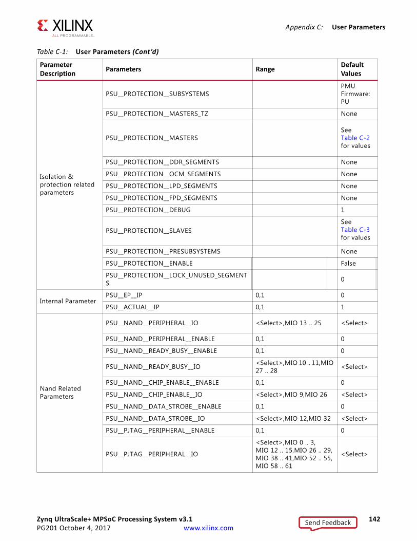
Zynq UltraScale+ MPSoC Processing System v3.1 142PG201 October 4, 2017 www.xilinx.com
Appendix C: User Parameters
Isolation & protection related parameters
PSU__PROTECTION__SUBSYSTEMSPMU Firmware: PU
PSU__PROTECTION__MASTERS_TZ None
PSU__PROTECTION__MASTERSSee Table C-2for values
PSU__PROTECTION__DDR_SEGMENTS None
PSU__PROTECTION__OCM_SEGMENTS None
PSU__PROTECTION__LPD_SEGMENTS None
PSU__PROTECTION__FPD_SEGMENTS None
PSU__PROTECTION__DEBUG 1
PSU__PROTECTION__SLAVESSee Table C-3for values
PSU__PROTECTION__PRESUBSYSTEMS None
PSU__PROTECTION__ENABLE False
PSU__PROTECTION__LOCK_UNUSED_SEGMENTS 0
Internal ParameterPSU__EP__IP 0,1 0
PSU__ACTUAL__IP 0,1 1
Nand Related Parameters
PSU__NAND__PERIPHERAL__IO <Select>,MIO 13 .. 25 <Select>
PSU__NAND__PERIPHERAL__ENABLE 0,1 0
PSU__NAND__READY_BUSY__ENABLE 0,1 0
PSU__NAND__READY_BUSY__IO <Select>,MIO 10 .. 11,MIO 27 .. 28 <Select>
PSU__NAND__CHIP_ENABLE__ENABLE 0,1 0
PSU__NAND__CHIP_ENABLE__IO <Select>,MIO 9,MIO 26 <Select>
PSU__NAND__DATA_STROBE__ENABLE 0,1 0
PSU__NAND__DATA_STROBE__IO <Select>,MIO 12,MIO 32 <Select>
PSU__PJTAG__PERIPHERAL__ENABLE 0,1 0
PSU__PJTAG__PERIPHERAL__IO
<Select>,MIO 0 .. 3,MIO 12 .. 15,MIO 26 .. 29,MIO 38 .. 41,MIO 52 .. 55,MIO 58 .. 61
<Select>
Table C‐1: User Parameters (Cont’d)
Parameter Description
Parameters RangeDefault Values
Send Feedback
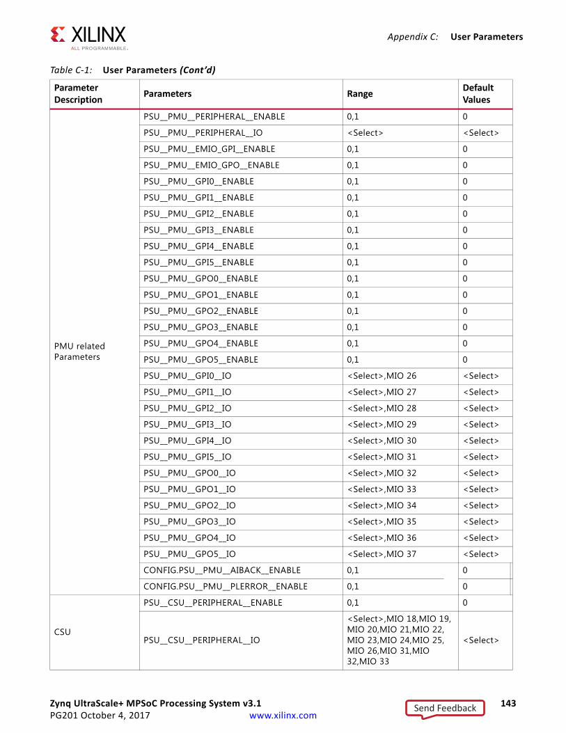
Zynq UltraScale+ MPSoC Processing System v3.1 143PG201 October 4, 2017 www.xilinx.com
Appendix C: User Parameters
PMU related Parameters
PSU__PMU__PERIPHERAL__ENABLE 0,1 0
PSU__PMU__PERIPHERAL__IO <Select> <Select>
PSU__PMU__EMIO_GPI__ENABLE 0,1 0
PSU__PMU__EMIO_GPO__ENABLE 0,1 0
PSU__PMU__GPI0__ENABLE 0,1 0
PSU__PMU__GPI1__ENABLE 0,1 0
PSU__PMU__GPI2__ENABLE 0,1 0
PSU__PMU__GPI3__ENABLE 0,1 0
PSU__PMU__GPI4__ENABLE 0,1 0
PSU__PMU__GPI5__ENABLE 0,1 0
PSU__PMU__GPO0__ENABLE 0,1 0
PSU__PMU__GPO1__ENABLE 0,1 0
PSU__PMU__GPO2__ENABLE 0,1 0
PSU__PMU__GPO3__ENABLE 0,1 0
PSU__PMU__GPO4__ENABLE 0,1 0
PSU__PMU__GPO5__ENABLE 0,1 0
PSU__PMU__GPI0__IO <Select>,MIO 26 <Select>
PSU__PMU__GPI1__IO <Select>,MIO 27 <Select>
PSU__PMU__GPI2__IO <Select>,MIO 28 <Select>
PSU__PMU__GPI3__IO <Select>,MIO 29 <Select>
PSU__PMU__GPI4__IO <Select>,MIO 30 <Select>
PSU__PMU__GPI5__IO <Select>,MIO 31 <Select>
PSU__PMU__GPO0__IO <Select>,MIO 32 <Select>
PSU__PMU__GPO1__IO <Select>,MIO 33 <Select>
PSU__PMU__GPO2__IO <Select>,MIO 34 <Select>
PSU__PMU__GPO3__IO <Select>,MIO 35 <Select>
PSU__PMU__GPO4__IO <Select>,MIO 36 <Select>
PSU__PMU__GPO5__IO <Select>,MIO 37 <Select>
CONFIG.PSU__PMU__AIBACK__ENABLE 0,1 0
CONFIG.PSU__PMU__PLERROR__ENABLE 0,1 0
CSU
PSU__CSU__PERIPHERAL__ENABLE 0,1 0
PSU__CSU__PERIPHERAL__IO
<Select>,MIO 18,MIO 19,MIO 20,MIO 21,MIO 22,MIO 23,MIO 24,MIO 25,MIO 26,MIO 31,MIO 32,MIO 33
<Select>
Table C‐1: User Parameters (Cont’d)
Parameter Description
Parameters RangeDefault Values
Send Feedback
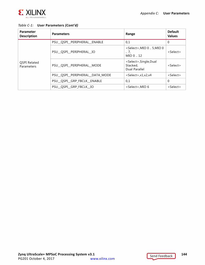
Zynq UltraScale+ MPSoC Processing System v3.1 144PG201 October 4, 2017 www.xilinx.com
Appendix C: User Parameters
QSPI Related Parameters
PSU__QSPI__PERIPHERAL__ENABLE 0,1 0
PSU__QSPI__PERIPHERAL__IO<Select>,MIO 0 .. 5,MIO 0 .. 7,MIO 0 .. 12
<Select>
PSU__QSPI__PERIPHERAL__MODE<Select>,Single,Dual Stacked,Dual Parallel
<Select>
PSU__QSPI__PERIPHERAL__DATA_MODE <Select>,x1,x2,x4 <Select>
PSU__QSPI__GRP_FBCLK__ENABLE 0,1 0
PSU__QSPI__GRP_FBCLK__IO <Select>,MIO 6 <Select>
Table C‐1: User Parameters (Cont’d)
Parameter Description
Parameters RangeDefault Values
Send Feedback
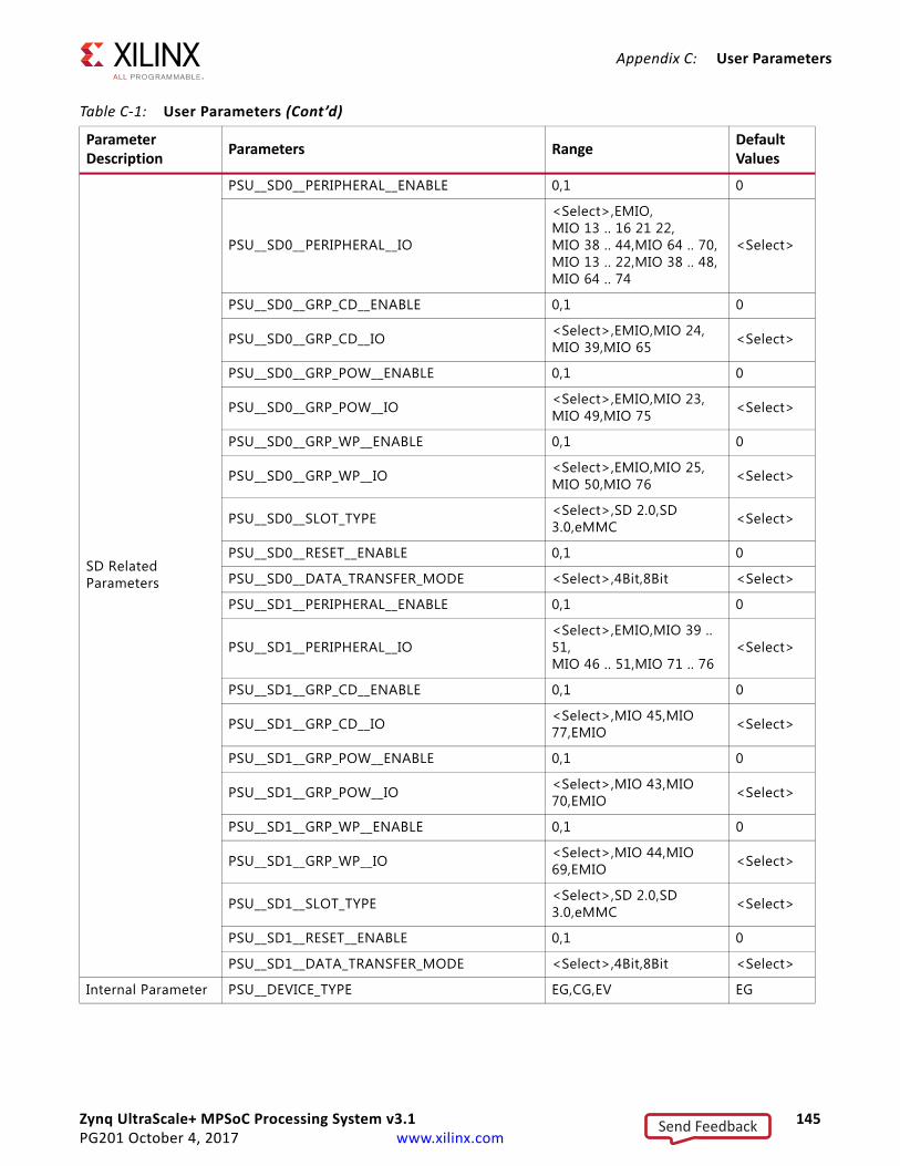
Zynq UltraScale+ MPSoC Processing System v3.1 145PG201 October 4, 2017 www.xilinx.com
Appendix C: User Parameters
SD Related Parameters
PSU__SD0__PERIPHERAL__ENABLE 0,1 0
PSU__SD0__PERIPHERAL__IO
<Select>,EMIO,MIO 13 .. 16 21 22,MIO 38 .. 44,MIO 64 .. 70,MIO 13 .. 22,MIO 38 .. 48,MIO 64 .. 74
<Select>
PSU__SD0__GRP_CD__ENABLE 0,1 0
PSU__SD0__GRP_CD__IO <Select>,EMIO,MIO 24,MIO 39,MIO 65 <Select>
PSU__SD0__GRP_POW__ENABLE 0,1 0
PSU__SD0__GRP_POW__IO <Select>,EMIO,MIO 23,MIO 49,MIO 75 <Select>
PSU__SD0__GRP_WP__ENABLE 0,1 0
PSU__SD0__GRP_WP__IO <Select>,EMIO,MIO 25,MIO 50,MIO 76 <Select>
PSU__SD0__SLOT_TYPE <Select>,SD 2.0,SD 3.0,eMMC <Select>
PSU__SD0__RESET__ENABLE 0,1 0
PSU__SD0__DATA_TRANSFER_MODE <Select>,4Bit,8Bit <Select>
PSU__SD1__PERIPHERAL__ENABLE 0,1 0
PSU__SD1__PERIPHERAL__IO<Select>,EMIO,MIO 39 .. 51,MIO 46 .. 51,MIO 71 .. 76
<Select>
PSU__SD1__GRP_CD__ENABLE 0,1 0
PSU__SD1__GRP_CD__IO <Select>,MIO 45,MIO 77,EMIO <Select>
PSU__SD1__GRP_POW__ENABLE 0,1 0
PSU__SD1__GRP_POW__IO <Select>,MIO 43,MIO 70,EMIO <Select>
PSU__SD1__GRP_WP__ENABLE 0,1 0
PSU__SD1__GRP_WP__IO <Select>,MIO 44,MIO 69,EMIO <Select>
PSU__SD1__SLOT_TYPE <Select>,SD 2.0,SD 3.0,eMMC <Select>
PSU__SD1__RESET__ENABLE 0,1 0
PSU__SD1__DATA_TRANSFER_MODE <Select>,4Bit,8Bit <Select>
Internal Parameter PSU__DEVICE_TYPE EG,CG,EV EG
Table C‐1: User Parameters (Cont’d)
Parameter Description
Parameters RangeDefault Values
Send Feedback
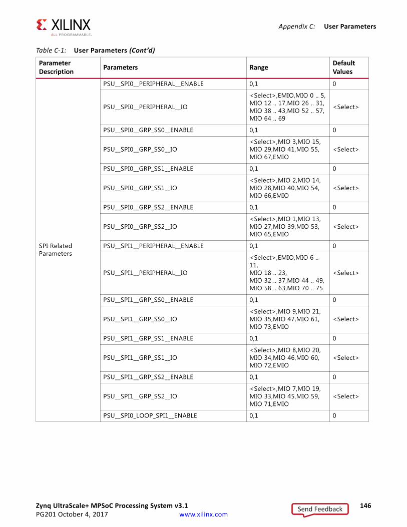
Zynq UltraScale+ MPSoC Processing System v3.1 146PG201 October 4, 2017 www.xilinx.com
Appendix C: User Parameters
SPI Related Parameters
PSU__SPI0__PERIPHERAL__ENABLE 0,1 0
PSU__SPI0__PERIPHERAL__IO
<Select>,EMIO,MIO 0 .. 5,MIO 12 .. 17,MIO 26 .. 31,MIO 38 .. 43,MIO 52 .. 57,MIO 64 .. 69
<Select>
PSU__SPI0__GRP_SS0__ENABLE 0,1 0
PSU__SPI0__GRP_SS0__IO<Select>,MIO 3,MIO 15,MIO 29,MIO 41,MIO 55,MIO 67,EMIO
<Select>
PSU__SPI0__GRP_SS1__ENABLE 0,1 0
PSU__SPI0__GRP_SS1__IO<Select>,MIO 2,MIO 14,MIO 28,MIO 40,MIO 54,MIO 66,EMIO
<Select>
PSU__SPI0__GRP_SS2__ENABLE 0,1 0
PSU__SPI0__GRP_SS2__IO<Select>,MIO 1,MIO 13,MIO 27,MIO 39,MIO 53,MIO 65,EMIO
<Select>
PSU__SPI1__PERIPHERAL__ENABLE 0,1 0
PSU__SPI1__PERIPHERAL__IO
<Select>,EMIO,MIO 6 .. 11,MIO 18 .. 23,MIO 32 .. 37,MIO 44 .. 49,MIO 58 .. 63,MIO 70 .. 75
<Select>
PSU__SPI1__GRP_SS0__ENABLE 0,1 0
PSU__SPI1__GRP_SS0__IO<Select>,MIO 9,MIO 21,MIO 35,MIO 47,MIO 61,MIO 73,EMIO
<Select>
PSU__SPI1__GRP_SS1__ENABLE 0,1 0
PSU__SPI1__GRP_SS1__IO<Select>,MIO 8,MIO 20,MIO 34,MIO 46,MIO 60,MIO 72,EMIO
<Select>
PSU__SPI1__GRP_SS2__ENABLE 0,1 0
PSU__SPI1__GRP_SS2__IO<Select>,MIO 7,MIO 19,MIO 33,MIO 45,MIO 59,MIO 71,EMIO
<Select>
PSU__SPI0_LOOP_SPI1__ENABLE 0,1 0
Table C‐1: User Parameters (Cont’d)
Parameter Description
Parameters RangeDefault Values
Send Feedback

Zynq UltraScale+ MPSoC Processing System v3.1 147PG201 October 4, 2017 www.xilinx.com
Appendix C: User Parameters
SWDT Related parameters
PSU__SWDT0__PERIPHERAL__ENABLE 0,1 0
PSU__SWDT0__CLOCK__ENABLE 0,1 0
PSU__SWDT0__RESET__ENABLE 0,1 0
PSU__SWDT0__PERIPHERAL__IO NA NA
PSU__SWDT0__CLOCK__IO
<Select>,EMIO,MIO 6,MIO 10,MIO 18,MIO 22,MIO 30,MIO 34,MIO 42,MIO 46,MIO 50,MIO 62,MIO 66,MIO 70,MIO 74
<Select>
PSU__SWDT0__RESET__IO
<Select>,EMIO,MIO 7,MIO 11,MIO 19,MIO 23,MIO 31,MIO 35,MIO 43,MIO 47,MIO 51,MIO 63,MIO 67,MIO 71,MIO 75
<Select>
PSU__SWDT1__PERIPHERAL__ENABLE 0,1 0
PSU__SWDT1__CLOCK__ENABLE 0,1 0
PSU__SWDT1__RESET__ENABLE 0,1 0
PSU__SWDT1__PERIPHERAL__IO NA NA
PSU__SWDT1__CLOCK__IO
<Select>,EMIO,MIO 4,MIO 8,MIO 16,MIO 20,MIO 24,MIO 32,MIO 36,MIO 44,MIO 48,MIO 56,MIO 64,MIO 68,MIO 72
<Select>
PSU__SWDT1__RESET__IO
<Select>,EMIO,MIO 5,MIO 9,MIO 17,MIO 21,MIO 25,MIO 33,MIO 37,MIO 45,MIO 49,MIO 57,MIO 65,MIO 69,MIO 73
<Select>
UART Baud rate PSU__UART0__BAUD_RATE
<Select>,110,300,1200,2400,4800,9600,19200,38400,57600,115200,128000,230400,460800,921600
<Select>
Table C‐1: User Parameters (Cont’d)
Parameter Description
Parameters RangeDefault Values
Send Feedback

Zynq UltraScale+ MPSoC Processing System v3.1 148PG201 October 4, 2017 www.xilinx.com
Appendix C: User Parameters
Trace Related Parameters
PSU__TRACE__PERIPHERAL__ENABLE 0,1 0
PSU__TRACE__PERIPHERAL__IO<Select>,MIO 0 .. 17,MIO 26 .. 43,MIO 52 .. 69,EMIO
<Select>
PSU__TRACE__WIDTH <Select>,2Bit,4Bit,8Bit,16Bit,32Bit <Select>
PSU__TRACE__INTERNAL_WIDTH 2,4,8,16,32 32
Table C‐1: User Parameters (Cont’d)
Parameter Description
Parameters RangeDefault Values
Send Feedback

Zynq UltraScale+ MPSoC Processing System v3.1 149PG201 October 4, 2017 www.xilinx.com
Appendix C: User Parameters
TTC Related Parameters
PSU__TTC0__PERIPHERAL__ENABLE 0,1 0
PSU__TTC0__CLOCK__ENABLE 0,1 0
PSU__TTC0__WAVEOUT__ENABLE 0,1 0
PSU__TTC0__CLOCK__IO
<Select>,EMIO,MIO 6,MIO 14,MIO 22,MIO 30,MIO 38,MIO 46,MIO 54,MIO 62,MIO 70
<Select>
PSU__TTC0__WAVEOUT__IO
<Select>,EMIO,MIO 7,MIO 15,MIO 23,MIO 31,MIO 39,MIO 47,MIO 55,MIO 63,MIO 71
<Select>
PSU__TTC0__PERIPHERAL__IO NA NA
PSU__TTC1__PERIPHERAL__ENABLE 0,1 0
PSU__TTC1__PERIPHERAL__IO NA NA
UART Baud rate PSU__UART1__BAUD_RATE
<Select>,110,300,1200,2400,4800,9600,19200,38400,57600,115200,128000,230400,460800,921600
<Select>
Table C‐1: User Parameters (Cont’d)
Parameter Description
Parameters RangeDefault Values
Send Feedback

Zynq UltraScale+ MPSoC Processing System v3.1 150PG201 October 4, 2017 www.xilinx.com
Appendix C: User Parameters
TTC Related Parameters
PSU__TTC1__CLOCK__ENABLE 0,1 0
PSU__TTC1__WAVEOUT__ENABLE 0,1 0
PSU__TTC1__CLOCK__IO
<Select>,EMIO,MIO 4,MIO 12,MIO 20,MIO 28,MIO 36,MIO 44,MIO 52,MIO 60,MIO 68
<Select>
PSU__TTC1__WAVEOUT__IO
<Select>,EMIO,MIO 5,MIO 13,MIO 21,MIO 29,MIO 37,MIO 45,MIO 53,MIO 61,MIO 69
<Select>
PSU__TTC2__PERIPHERAL__ENABLE 0,1 0
PSU__TTC2__PERIPHERAL__IO NA NA
PSU__TTC2__CLOCK__ENABLE 0,1 0
PSU__TTC2__WAVEOUT__ENABLE 0,1 0
PSU__TTC2__CLOCK__IO
<Select>,EMIO,MIO 2,MIO 10,MIO 18,MIO 26,MIO 34,MIO 42,MIO 50,MIO 58,MIO 66
<Select>
PSU__TTC2__WAVEOUT__IO
<Select>,EMIO,MIO 3,MIO 11,MIO 19,MIO 27,MIO 35,MIO 43,MIO 51,MIO 59,MIO 67
<Select>
PSU__TTC3__PERIPHERAL__ENABLE 0,1 0
PSU__TTC3__PERIPHERAL__IO NA NA
PSU__TTC3__CLOCK__ENABLE 0,1 0
PSU__TTC3__WAVEOUT__ENABLE 0,1 0
TTC Related
Parameters
(continued)
PSU__TTC3__CLOCK__IO
<Select>,EMIO,MIO 0,MIO 8,MIO 16,MIO 24,MIO 32,MIO 40,MIO 48,MIO 56,MIO 64
<Select>
PSU__TTC3__WAVEOUT__IO
<Select>,EMIO,MIO 1,MIO 9,MIO 17,MIO 25,MIO 33,MIO 41,MIO 49,MIO 57,MIO 65
<Select>
Table C‐1: User Parameters (Cont’d)
Parameter Description
Parameters RangeDefault Values
Send Feedback

Zynq UltraScale+ MPSoC Processing System v3.1 151PG201 October 4, 2017 www.xilinx.com
Appendix C: User Parameters
DDR Related Parameters
PSU__DDRC__AL 0
PSU__DDRC__BANK_ADDR_COUNT 3
PSU__DDRC__BUS_WIDTH 32 Bit,64 Bit 64 Bit
PSU__DDRC__CL NA 7
PSU__DDRC__CLOCK_STOP_EN 0,1 0
PSU__DDRC__COL_ADDR_COUNT 10
PSU__DDRC__RANK_ADDR_COUNT 0
PSU__DDRC__CWL NA 7
PSU__DDRC__BG_ADDR_COUNT 1.000000,2.000000 NA
PSU__DDRC__DEVICE_CAPACITY512 MBits,1024 MBits,2048 MBits,4096 MBits,8192 MBits
2048 MBits
PSU__DDRC__DRAM_WIDTH 8 Bits,16 Bits 8 Bits
PSU__DDRC__ECC Disabled,Enabled Disabled
PSU__DDRC__ECC_SCRUB 0,1 0
PSU__DDRC__ENABLE 0,1 1
PSU__DDRC__FREQ_MHZ -2,-1 1
PSU__DDRC__HIGH_TEMP <Select> <Select>
PSU__DDRC__MEMORY_TYPE
LPDDR 3,DDR 3,DDR 3 (Low Voltage),DDR 4,LPDDR 4
DDR 4
PSU__DDRC__PARTNO <Select> <Select>
PSU__DDRC__ROW_ADDR_COUNT -2,-1 15
PSU__DDRC__SPEED_BIN
DDR3_800D,DDR3_800E,DDR3_1066E,DDR3_1066F,DDR3_1066G,DDR3_1333F,DDR3_1333G,DDR3_1333H,DDR3_1333J,DDR3_1600G,DDR3_1600H,DDR3_1600J,DDR3_1600K,DDR3_1866J,DDR3_1866K,DDR3_1866L,DDR3_1866M,DDR3_2133N
DDR4_1600J
PSU__DDRC__T_FAW -0.1,100 35
Table C‐1: User Parameters (Cont’d)
Parameter Description
Parameters RangeDefault Values
Send Feedback

Zynq UltraScale+ MPSoC Processing System v3.1 152PG201 October 4, 2017 www.xilinx.com
Appendix C: User Parameters
DDR Related Parameters
(continued)
PSU__DDRC__T_RCD -2,-1 10
PSU__DDRC__T_RP -0.1,100 10
PSU__DDRC__TRAIN_DATA_EYE 0,1 1
PSU__DDRC__TRAIN_READ_GATE 0,1 1
PSU__DDRC__TRAIN_WRITE_LEVEL 0,1 1
PSU__DDRC__VREF 0,1 1
PSU__DDRC__VIDEO_BUFFER_SIZE 0,1,2,4,8,16,32 0
PSU__DDRC__BRC_MAPPING ROW_BANK_COL,BANK_ROW_COL
ROW_BANK_COL
PSU__DDRC__DIMM_ADDR_MIRROR 0,1 0
PSU__DDRC__STATIC_RD_MODE 0,1 0
PSU__DDRC__DDR4_MAXPWR_SAVING_EN 0,1 NA
PSU__DDRC__PWR_DOWN_EN 0,1 0
PSU__DDRC__DEEP_PWR_DOWN_EN <Select>,0,1 <Select>
PSU__DDRC__PLL_BYPASS 0,1 0
PSU__DDRC__DDR4_T_REF_MODE 0,1 NA
PSU__DDRC__DDR4_T_REF_RANGE Normal (0-85),High (95 Max) NA
PSU__DDRC__PHY_DBI_MODE 0,1 0
PSU__DDRC__DM_DBI
NO_DM_NO_DBI,NO_DM_DBI_RD_WR,NO_DM_DBI_RD,NO_DM_DBI_WR,DM_DBI_RD_WR,DM_DBI_RD,DM_DBI_WR,DM_NO_DBI
DM_NO_DBI
PSU__DDRC__COMPONENTS Components,UDIMM,RDIMM
Components
PSU__DDRC__PARITY_ENABLE 0,1 NA
PSU__DDRC__DDR4_CAL_MODE_ENABLE 0,1 NA
PSU__DDRC__DDR4_CRC_CONTROL 0,1 NA
PSU__DDRC__FGRM 1X,2X,4X 1X
PSU__DDRC__VENDOR_PART OTHERS,SAMSUNG,HYNIX OTHERS
Table C‐1: User Parameters (Cont’d)
Parameter Description
Parameters RangeDefault Values
Send Feedback
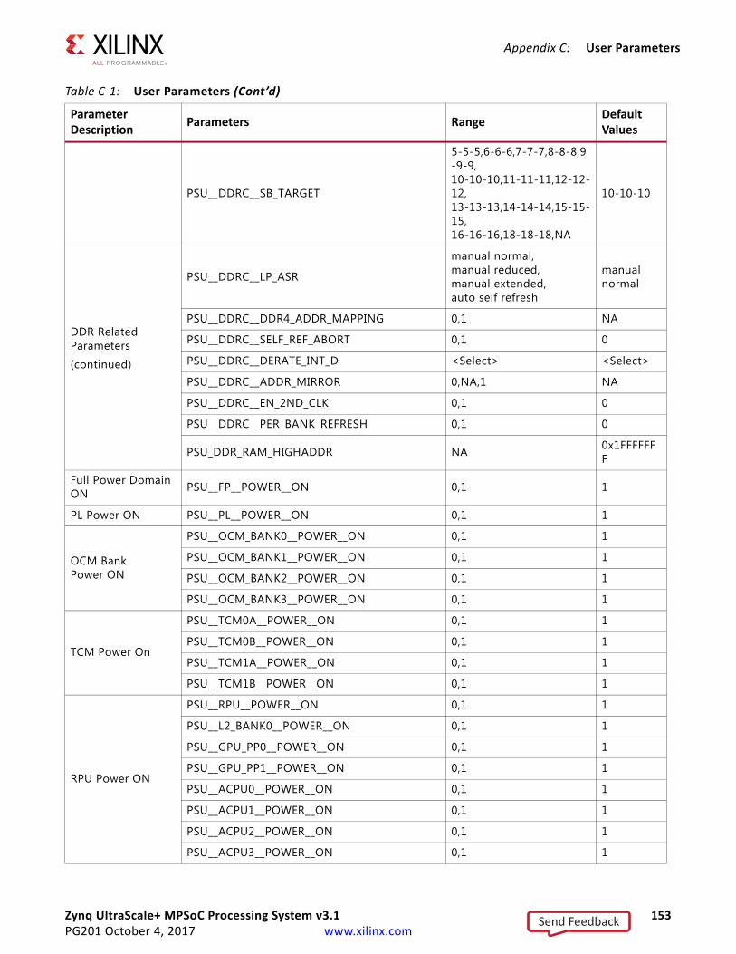
Zynq UltraScale+ MPSoC Processing System v3.1 153PG201 October 4, 2017 www.xilinx.com
Appendix C: User Parameters
PSU__DDRC__SB_TARGET
5-5-5,6-6-6,7-7-7,8-8-8,9-9-9,10-10-10,11-11-11,12-12-12,13-13-13,14-14-14,15-15-15,16-16-16,18-18-18,NA
10-10-10
DDR Related Parameters
(continued)
PSU__DDRC__LP_ASR
manual normal,manual reduced,manual extended,auto self refresh
manual normal
PSU__DDRC__DDR4_ADDR_MAPPING 0,1 NA
PSU__DDRC__SELF_REF_ABORT 0,1 0
PSU__DDRC__DERATE_INT_D <Select> <Select>
PSU__DDRC__ADDR_MIRROR 0,NA,1 NA
PSU__DDRC__EN_2ND_CLK 0,1 0
PSU__DDRC__PER_BANK_REFRESH 0,1 0
PSU_DDR_RAM_HIGHADDR NA 0x1FFFFFFF
Full Power Domain ON PSU__FP__POWER__ON 0,1 1
PL Power ON PSU__PL__POWER__ON 0,1 1
OCM Bank Power ON
PSU__OCM_BANK0__POWER__ON 0,1 1
PSU__OCM_BANK1__POWER__ON 0,1 1
PSU__OCM_BANK2__POWER__ON 0,1 1
PSU__OCM_BANK3__POWER__ON 0,1 1
TCM Power On
PSU__TCM0A__POWER__ON 0,1 1
PSU__TCM0B__POWER__ON 0,1 1
PSU__TCM1A__POWER__ON 0,1 1
PSU__TCM1B__POWER__ON 0,1 1
RPU Power ON
PSU__RPU__POWER__ON 0,1 1
PSU__L2_BANK0__POWER__ON 0,1 1
PSU__GPU_PP0__POWER__ON 0,1 1
PSU__GPU_PP1__POWER__ON 0,1 1
PSU__ACPU0__POWER__ON 0,1 1
PSU__ACPU1__POWER__ON 0,1 1
PSU__ACPU2__POWER__ON 0,1 1
PSU__ACPU3__POWER__ON 0,1 1
Table C‐1: User Parameters (Cont’d)
Parameter Description
Parameters RangeDefault Values
Send Feedback
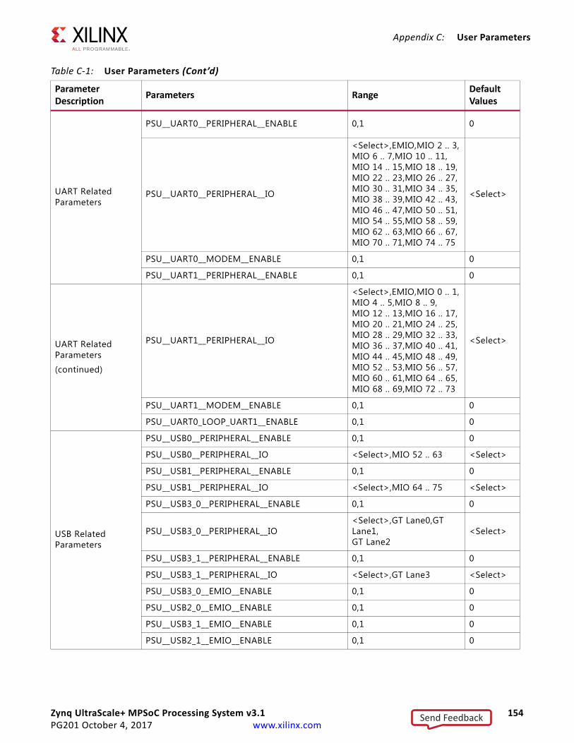
Zynq UltraScale+ MPSoC Processing System v3.1 154PG201 October 4, 2017 www.xilinx.com
Appendix C: User Parameters
UART Related Parameters
PSU__UART0__PERIPHERAL__ENABLE 0,1 0
PSU__UART0__PERIPHERAL__IO
<Select>,EMIO,MIO 2 .. 3,MIO 6 .. 7,MIO 10 .. 11,MIO 14 .. 15,MIO 18 .. 19,MIO 22 .. 23,MIO 26 .. 27,MIO 30 .. 31,MIO 34 .. 35,MIO 38 .. 39,MIO 42 .. 43,MIO 46 .. 47,MIO 50 .. 51,MIO 54 .. 55,MIO 58 .. 59,MIO 62 .. 63,MIO 66 .. 67,MIO 70 .. 71,MIO 74 .. 75
<Select>
PSU__UART0__MODEM__ENABLE 0,1 0
PSU__UART1__PERIPHERAL__ENABLE 0,1 0
UART Related Parameters
(continued)
PSU__UART1__PERIPHERAL__IO
<Select>,EMIO,MIO 0 .. 1,MIO 4 .. 5,MIO 8 .. 9,MIO 12 .. 13,MIO 16 .. 17,MIO 20 .. 21,MIO 24 .. 25,MIO 28 .. 29,MIO 32 .. 33,MIO 36 .. 37,MIO 40 .. 41,MIO 44 .. 45,MIO 48 .. 49,MIO 52 .. 53,MIO 56 .. 57,MIO 60 .. 61,MIO 64 .. 65,MIO 68 .. 69,MIO 72 .. 73
<Select>
PSU__UART1__MODEM__ENABLE 0,1 0
PSU__UART0_LOOP_UART1__ENABLE 0,1 0
USB Related Parameters
PSU__USB0__PERIPHERAL__ENABLE 0,1 0
PSU__USB0__PERIPHERAL__IO <Select>,MIO 52 .. 63 <Select>
PSU__USB1__PERIPHERAL__ENABLE 0,1 0
PSU__USB1__PERIPHERAL__IO <Select>,MIO 64 .. 75 <Select>
PSU__USB3_0__PERIPHERAL__ENABLE 0,1 0
PSU__USB3_0__PERIPHERAL__IO<Select>,GT Lane0,GT Lane1,GT Lane2
<Select>
PSU__USB3_1__PERIPHERAL__ENABLE 0,1 0
PSU__USB3_1__PERIPHERAL__IO <Select>,GT Lane3 <Select>
PSU__USB3_0__EMIO__ENABLE 0,1 0
PSU__USB2_0__EMIO__ENABLE 0,1 0
PSU__USB3_1__EMIO__ENABLE 0,1 0
PSU__USB2_1__EMIO__ENABLE 0,1 0
Table C‐1: User Parameters (Cont’d)
Parameter Description
Parameters RangeDefault Values
Send Feedback

Zynq UltraScale+ MPSoC Processing System v3.1 155PG201 October 4, 2017 www.xilinx.com
Appendix C: User Parameters
PS PL Interface related Parameters
PSU__USE__M_AXI_GP0 0,1 0
PSU__MAXIGP0__DATA_WIDTH 128,64,32 128
PSU__USE__M_AXI_GP1 0,1 0
PSU__MAXIGP1__DATA_WIDTH 128,64,32 128
PSU__USE__M_AXI_GP2 0,1 1
PSU__MAXIGP2__DATA_WIDTH 128,64,32 128
PSU__USE__S_AXI_ACP 0,1 0
PSU__USE__S_AXI_GP0 0,1 0
PSU__USE_DIFF_RW_CLK_GP0 0,1 0
PSU__SAXIGP0__DATA_WIDTH 128,64,32 128
PSU__USE__S_AXI_GP1 0,1 0
PSU__USE_DIFF_RW_CLK_GP1 0,1 0
PSU__SAXIGP1__DATA_WIDTH 128,64,32 128
PS PL Interface related Parameters
(continued)
PSU__USE__S_AXI_GP2 0,1 0
PSU__USE_DIFF_RW_CLK_GP2 0,1 0
PSU__SAXIGP2__DATA_WIDTH 128,64,32 128
PSU__USE__S_AXI_GP3 0,1 0
PSU__USE_DIFF_RW_CLK_GP3 0,1 0
PSU__SAXIGP3__DATA_WIDTH 128,64,32 128
PSU__USE__S_AXI_GP4 0,1 0
PSU__USE_DIFF_RW_CLK_GP4 0,1 0
PSU__SAXIGP4__DATA_WIDTH 128,64,32 128
PSU__USE__S_AXI_GP5 0,1 0
PSU__USE_DIFF_RW_CLK_GP5 0,1 0
PSU__SAXIGP5__DATA_WIDTH 128,64,32 128
PSU__USE__S_AXI_GP6 0,1 0
PSU__USE_DIFF_RW_CLK_GP6 0,1 0
PSU__SAXIGP6__DATA_WIDTH 128,64,32 128
PSU__USE__S_AXI_ACE 0,1 0
PSU__USE__FABRIC__RST 0,1 1
Table C‐1: User Parameters (Cont’d)
Parameter Description
Parameters RangeDefault Values
Send Feedback
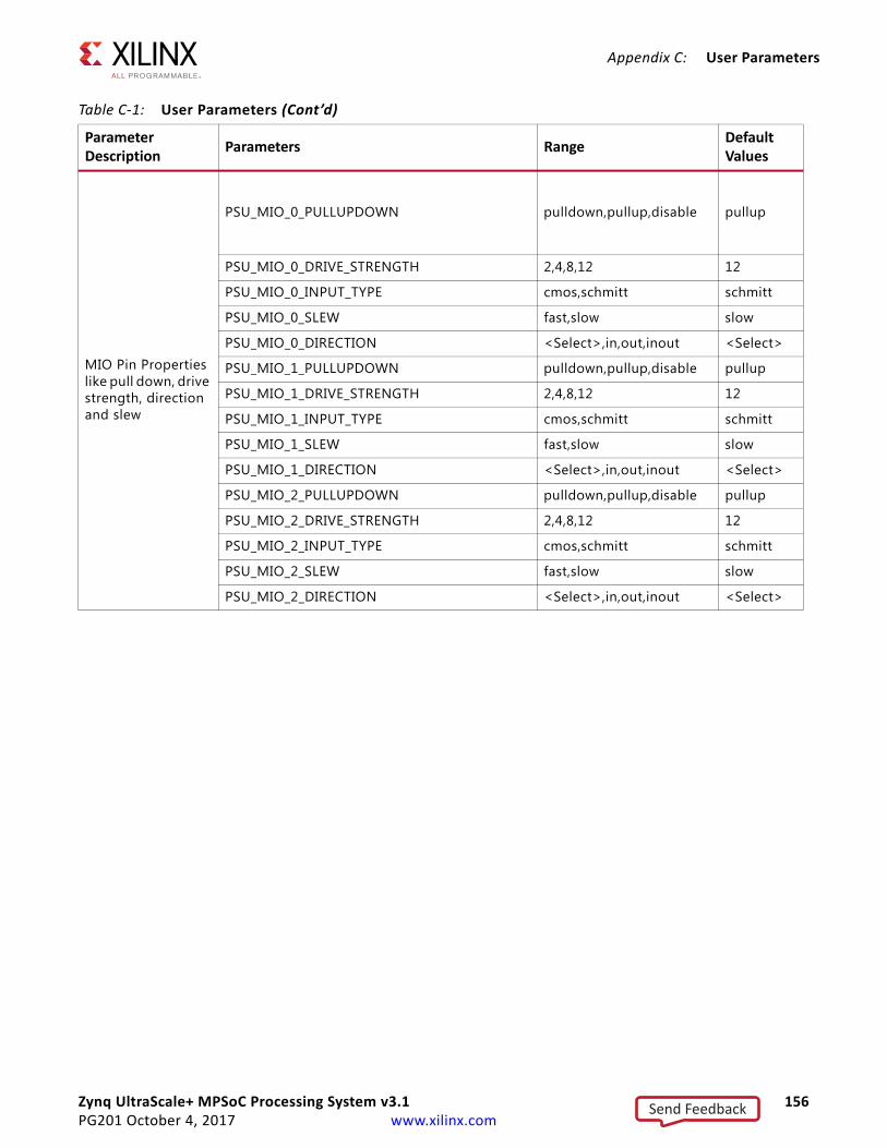
Zynq UltraScale+ MPSoC Processing System v3.1 156PG201 October 4, 2017 www.xilinx.com
Appendix C: User Parameters
MIO Pin Properties like pull down, drive strength, direction and slew
PSU_MIO_0_PULLUPDOWN pulldown,pullup,disable pullup
PSU_MIO_0_DRIVE_STRENGTH 2,4,8,12 12
PSU_MIO_0_INPUT_TYPE cmos,schmitt schmitt
PSU_MIO_0_SLEW fast,slow slow
PSU_MIO_0_DIRECTION <Select>,in,out,inout <Select>
PSU_MIO_1_PULLUPDOWN pulldown,pullup,disable pullup
PSU_MIO_1_DRIVE_STRENGTH 2,4,8,12 12
PSU_MIO_1_INPUT_TYPE cmos,schmitt schmitt
PSU_MIO_1_SLEW fast,slow slow
PSU_MIO_1_DIRECTION <Select>,in,out,inout <Select>
PSU_MIO_2_PULLUPDOWN pulldown,pullup,disable pullup
PSU_MIO_2_DRIVE_STRENGTH 2,4,8,12 12
PSU_MIO_2_INPUT_TYPE cmos,schmitt schmitt
PSU_MIO_2_SLEW fast,slow slow
PSU_MIO_2_DIRECTION <Select>,in,out,inout <Select>
Table C‐1: User Parameters (Cont’d)
Parameter Description
Parameters RangeDefault Values
Send Feedback
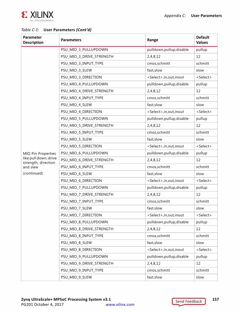
Zynq UltraScale+ MPSoC Processing System v3.1 157PG201 October 4, 2017 www.xilinx.com
Appendix C: User Parameters
MIO Pin Properties like pull down, drive strength, direction and slew
(continued)
PSU_MIO_3_PULLUPDOWN pulldown,pullup,disable pullup
PSU_MIO_3_DRIVE_STRENGTH 2,4,8,12 12
PSU_MIO_3_INPUT_TYPE cmos,schmitt schmitt
PSU_MIO_3_SLEW fast,slow slow
PSU_MIO_3_DIRECTION <Select>,in,out,inout <Select>
PSU_MIO_4_PULLUPDOWN pulldown,pullup,disable pullup
PSU_MIO_4_DRIVE_STRENGTH 2,4,8,12 12
PSU_MIO_4_INPUT_TYPE cmos,schmitt schmitt
PSU_MIO_4_SLEW fast,slow slow
PSU_MIO_4_DIRECTION <Select>,in,out,inout <Select>
PSU_MIO_5_PULLUPDOWN pulldown,pullup,disable pullup
PSU_MIO_5_DRIVE_STRENGTH 2,4,8,12 12
PSU_MIO_5_INPUT_TYPE cmos,schmitt schmitt
PSU_MIO_5_SLEW fast,slow slow
PSU_MIO_5_DIRECTION <Select>,in,out,inout <Select>
PSU_MIO_6_PULLUPDOWN pulldown,pullup,disable pullup
PSU_MIO_6_DRIVE_STRENGTH 2,4,8,12 12
PSU_MIO_6_INPUT_TYPE cmos,schmitt schmitt
PSU_MIO_6_SLEW fast,slow slow
PSU_MIO_6_DIRECTION <Select>,in,out,inout <Select>
PSU_MIO_7_PULLUPDOWN pulldown,pullup,disable pullup
PSU_MIO_7_DRIVE_STRENGTH 2,4,8,12 12
PSU_MIO_7_INPUT_TYPE cmos,schmitt schmitt
PSU_MIO_7_SLEW fast,slow slow
PSU_MIO_7_DIRECTION <Select>,in,out,inout <Select>
PSU_MIO_8_PULLUPDOWN pulldown,pullup,disable pullup
PSU_MIO_8_DRIVE_STRENGTH 2,4,8,12 12
PSU_MIO_8_INPUT_TYPE cmos,schmitt schmitt
PSU_MIO_8_SLEW fast,slow slow
PSU_MIO_8_DIRECTION <Select>,in,out,inout <Select>
PSU_MIO_9_PULLUPDOWN pulldown,pullup,disable pullup
PSU_MIO_9_DRIVE_STRENGTH 2,4,8,12 12
PSU_MIO_9_INPUT_TYPE cmos,schmitt schmitt
PSU_MIO_9_SLEW fast,slow slow
Table C‐1: User Parameters (Cont’d)
Parameter Description
Parameters RangeDefault Values
Send Feedback
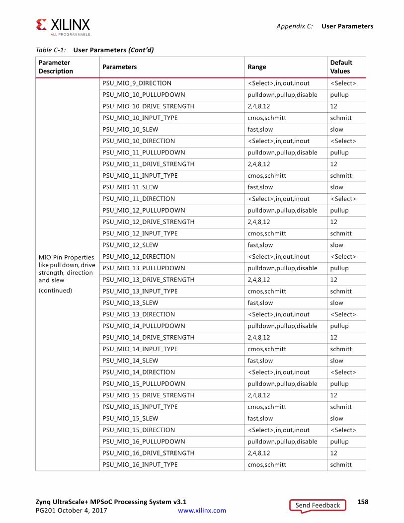
Zynq UltraScale+ MPSoC Processing System v3.1 158PG201 October 4, 2017 www.xilinx.com
Appendix C: User Parameters
MIO Pin Properties like pull down, drive strength, direction and slew
(continued)
PSU_MIO_9_DIRECTION <Select>,in,out,inout <Select>
PSU_MIO_10_PULLUPDOWN pulldown,pullup,disable pullup
PSU_MIO_10_DRIVE_STRENGTH 2,4,8,12 12
PSU_MIO_10_INPUT_TYPE cmos,schmitt schmitt
PSU_MIO_10_SLEW fast,slow slow
PSU_MIO_10_DIRECTION <Select>,in,out,inout <Select>
PSU_MIO_11_PULLUPDOWN pulldown,pullup,disable pullup
PSU_MIO_11_DRIVE_STRENGTH 2,4,8,12 12
PSU_MIO_11_INPUT_TYPE cmos,schmitt schmitt
PSU_MIO_11_SLEW fast,slow slow
PSU_MIO_11_DIRECTION <Select>,in,out,inout <Select>
PSU_MIO_12_PULLUPDOWN pulldown,pullup,disable pullup
PSU_MIO_12_DRIVE_STRENGTH 2,4,8,12 12
PSU_MIO_12_INPUT_TYPE cmos,schmitt schmitt
PSU_MIO_12_SLEW fast,slow slow
PSU_MIO_12_DIRECTION <Select>,in,out,inout <Select>
PSU_MIO_13_PULLUPDOWN pulldown,pullup,disable pullup
PSU_MIO_13_DRIVE_STRENGTH 2,4,8,12 12
PSU_MIO_13_INPUT_TYPE cmos,schmitt schmitt
PSU_MIO_13_SLEW fast,slow slow
PSU_MIO_13_DIRECTION <Select>,in,out,inout <Select>
PSU_MIO_14_PULLUPDOWN pulldown,pullup,disable pullup
PSU_MIO_14_DRIVE_STRENGTH 2,4,8,12 12
PSU_MIO_14_INPUT_TYPE cmos,schmitt schmitt
PSU_MIO_14_SLEW fast,slow slow
PSU_MIO_14_DIRECTION <Select>,in,out,inout <Select>
PSU_MIO_15_PULLUPDOWN pulldown,pullup,disable pullup
PSU_MIO_15_DRIVE_STRENGTH 2,4,8,12 12
PSU_MIO_15_INPUT_TYPE cmos,schmitt schmitt
PSU_MIO_15_SLEW fast,slow slow
PSU_MIO_15_DIRECTION <Select>,in,out,inout <Select>
PSU_MIO_16_PULLUPDOWN pulldown,pullup,disable pullup
PSU_MIO_16_DRIVE_STRENGTH 2,4,8,12 12
PSU_MIO_16_INPUT_TYPE cmos,schmitt schmitt
Table C‐1: User Parameters (Cont’d)
Parameter Description
Parameters RangeDefault Values
Send Feedback
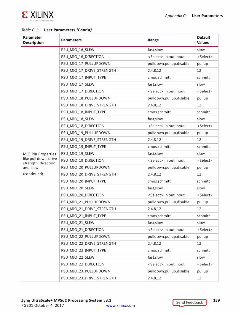
Zynq UltraScale+ MPSoC Processing System v3.1 159PG201 October 4, 2017 www.xilinx.com
Appendix C: User Parameters
MIO Pin Properties like pull down, drive strength, direction and slew
(continued)
PSU_MIO_16_SLEW fast,slow slow
PSU_MIO_16_DIRECTION <Select>,in,out,inout <Select>
PSU_MIO_17_PULLUPDOWN pulldown,pullup,disable pullup
PSU_MIO_17_DRIVE_STRENGTH 2,4,8,12 12
PSU_MIO_17_INPUT_TYPE cmos,schmitt schmitt
PSU_MIO_17_SLEW fast,slow slow
PSU_MIO_17_DIRECTION <Select>,in,out,inout <Select>
PSU_MIO_18_PULLUPDOWN pulldown,pullup,disable pullup
PSU_MIO_18_DRIVE_STRENGTH 2,4,8,12 12
PSU_MIO_18_INPUT_TYPE cmos,schmitt schmitt
PSU_MIO_18_SLEW fast,slow slow
PSU_MIO_18_DIRECTION <Select>,in,out,inout <Select>
PSU_MIO_19_PULLUPDOWN pulldown,pullup,disable pullup
PSU_MIO_19_DRIVE_STRENGTH 2,4,8,12 12
PSU_MIO_19_INPUT_TYPE cmos,schmitt schmitt
PSU_MIO_19_SLEW fast,slow slow
PSU_MIO_19_DIRECTION <Select>,in,out,inout <Select>
PSU_MIO_20_PULLUPDOWN pulldown,pullup,disable pullup
PSU_MIO_20_DRIVE_STRENGTH 2,4,8,12 12
PSU_MIO_20_INPUT_TYPE cmos,schmitt schmitt
PSU_MIO_20_SLEW fast,slow slow
PSU_MIO_20_DIRECTION <Select>,in,out,inout <Select>
PSU_MIO_21_PULLUPDOWN pulldown,pullup,disable pullup
PSU_MIO_21_DRIVE_STRENGTH 2,4,8,12 12
PSU_MIO_21_INPUT_TYPE cmos,schmitt schmitt
PSU_MIO_21_SLEW fast,slow slow
PSU_MIO_21_DIRECTION <Select>,in,out,inout <Select>
PSU_MIO_22_PULLUPDOWN pulldown,pullup,disable pullup
PSU_MIO_22_DRIVE_STRENGTH 2,4,8,12 12
PSU_MIO_22_INPUT_TYPE cmos,schmitt schmitt
PSU_MIO_22_SLEW fast,slow slow
PSU_MIO_22_DIRECTION <Select>,in,out,inout <Select>
PSU_MIO_23_PULLUPDOWN pulldown,pullup,disable pullup
PSU_MIO_23_DRIVE_STRENGTH 2,4,8,12 12
Table C‐1: User Parameters (Cont’d)
Parameter Description
Parameters RangeDefault Values
Send Feedback

Zynq UltraScale+ MPSoC Processing System v3.1 160PG201 October 4, 2017 www.xilinx.com
Appendix C: User Parameters
MIO Pin Properties like pull down, drive strength, direction and slew
(continued)
PSU_MIO_23_INPUT_TYPE cmos,schmitt schmitt
PSU_MIO_23_SLEW fast,slow slow
PSU_MIO_23_DIRECTION <Select>,in,out,inout <Select>
PSU_MIO_24_PULLUPDOWN pulldown,pullup,disable pullup
PSU_MIO_24_DRIVE_STRENGTH 2,4,8,12 12
PSU_MIO_24_INPUT_TYPE cmos,schmitt schmitt
PSU_MIO_24_SLEW fast,slow slow
PSU_MIO_24_DIRECTION <Select>,in,out,inout <Select>
PSU_MIO_25_PULLUPDOWN pulldown,pullup,disable pullup
PSU_MIO_25_DRIVE_STRENGTH 2,4,8,12 12
PSU_MIO_25_INPUT_TYPE cmos,schmitt schmitt
PSU_MIO_25_SLEW fast,slow slow
PSU_MIO_25_DIRECTION <Select>,in,out,inout <Select>
PSU_MIO_26_PULLUPDOWN pulldown,pullup,disable pullup
PSU_MIO_26_DRIVE_STRENGTH 2,4,8,12 12
PSU_MIO_26_INPUT_TYPE cmos,schmitt schmitt
PSU_MIO_26_SLEW fast,slow slow
PSU_MIO_26_DIRECTION <Select>,in,out,inout <Select>
PSU_MIO_27_PULLUPDOWN pulldown,pullup,disable pullup
PSU_MIO_27_DRIVE_STRENGTH 2,4,8,12 12
PSU_MIO_27_INPUT_TYPE cmos,schmitt schmitt
PSU_MIO_27_SLEW fast,slow slow
PSU_MIO_27_DIRECTION <Select>,in,out,inout <Select>
PSU_MIO_28_PULLUPDOWN pulldown,pullup,disable pullup
PSU_MIO_28_DRIVE_STRENGTH 2,4,8,12 12
PSU_MIO_28_INPUT_TYPE cmos,schmitt schmitt
PSU_MIO_28_SLEW fast,slow slow
PSU_MIO_28_DIRECTION <Select>,in,out,inout <Select>
PSU_MIO_29_PULLUPDOWN pulldown,pullup,disable pullup
PSU_MIO_29_DRIVE_STRENGTH 2,4,8,12 12
PSU_MIO_29_INPUT_TYPE cmos,schmitt schmitt
PSU_MIO_29_SLEW fast,slow slow
PSU_MIO_29_DIRECTION <Select>,in,out,inout <Select>
PSU_MIO_30_PULLUPDOWN pulldown,pullup,disable pullup
Table C‐1: User Parameters (Cont’d)
Parameter Description
Parameters RangeDefault Values
Send Feedback
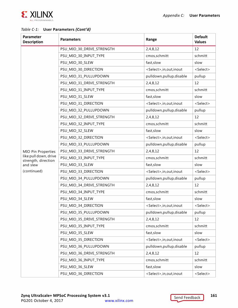
Zynq UltraScale+ MPSoC Processing System v3.1 161PG201 October 4, 2017 www.xilinx.com
Appendix C: User Parameters
MIO Pin Properties like pull down, drive strength, direction and slew
(continued)
PSU_MIO_30_DRIVE_STRENGTH 2,4,8,12 12
PSU_MIO_30_INPUT_TYPE cmos,schmitt schmitt
PSU_MIO_30_SLEW fast,slow slow
PSU_MIO_30_DIRECTION <Select>,in,out,inout <Select>
PSU_MIO_31_PULLUPDOWN pulldown,pullup,disable pullup
PSU_MIO_31_DRIVE_STRENGTH 2,4,8,12 12
PSU_MIO_31_INPUT_TYPE cmos,schmitt schmitt
PSU_MIO_31_SLEW fast,slow slow
PSU_MIO_31_DIRECTION <Select>,in,out,inout <Select>
PSU_MIO_32_PULLUPDOWN pulldown,pullup,disable pullup
PSU_MIO_32_DRIVE_STRENGTH 2,4,8,12 12
PSU_MIO_32_INPUT_TYPE cmos,schmitt schmitt
PSU_MIO_32_SLEW fast,slow slow
PSU_MIO_32_DIRECTION <Select>,in,out,inout <Select>
PSU_MIO_33_PULLUPDOWN pulldown,pullup,disable pullup
PSU_MIO_33_DRIVE_STRENGTH 2,4,8,12 12
PSU_MIO_33_INPUT_TYPE cmos,schmitt schmitt
PSU_MIO_33_SLEW fast,slow slow
PSU_MIO_33_DIRECTION <Select>,in,out,inout <Select>
PSU_MIO_34_PULLUPDOWN pulldown,pullup,disable pullup
PSU_MIO_34_DRIVE_STRENGTH 2,4,8,12 12
PSU_MIO_34_INPUT_TYPE cmos,schmitt schmitt
PSU_MIO_34_SLEW fast,slow slow
PSU_MIO_34_DIRECTION <Select>,in,out,inout <Select>
PSU_MIO_35_PULLUPDOWN pulldown,pullup,disable pullup
PSU_MIO_35_DRIVE_STRENGTH 2,4,8,12 12
PSU_MIO_35_INPUT_TYPE cmos,schmitt schmitt
PSU_MIO_35_SLEW fast,slow slow
PSU_MIO_35_DIRECTION <Select>,in,out,inout <Select>
PSU_MIO_36_PULLUPDOWN pulldown,pullup,disable pullup
PSU_MIO_36_DRIVE_STRENGTH 2,4,8,12 12
PSU_MIO_36_INPUT_TYPE cmos,schmitt schmitt
PSU_MIO_36_SLEW fast,slow slow
PSU_MIO_36_DIRECTION <Select>,in,out,inout <Select>
Table C‐1: User Parameters (Cont’d)
Parameter Description
Parameters RangeDefault Values
Send Feedback

Zynq UltraScale+ MPSoC Processing System v3.1 162PG201 October 4, 2017 www.xilinx.com
Appendix C: User Parameters
MIO Pin Properties like pull down, drive strength, direction and slew
(continued)
PSU_MIO_37_PULLUPDOWN pulldown,pullup,disable pullup
PSU_MIO_37_DRIVE_STRENGTH 2,4,8,12 12
PSU_MIO_37_INPUT_TYPE cmos,schmitt schmitt
PSU_MIO_37_SLEW fast,slow slow
PSU_MIO_37_DIRECTION <Select>,in,out,inout <Select>
PSU_MIO_38_PULLUPDOWN pulldown,pullup,disable pullup
PSU_MIO_38_DRIVE_STRENGTH 2,4,8,12 12
PSU_MIO_38_INPUT_TYPE cmos,schmitt schmitt
PSU_MIO_38_SLEW fast,slow slow
PSU_MIO_38_DIRECTION <Select>,in,out,inout <Select>
PSU_MIO_39_PULLUPDOWN pulldown,pullup,disable pullup
PSU_MIO_39_DRIVE_STRENGTH 2,4,8,12 12
PSU_MIO_39_INPUT_TYPE cmos,schmitt schmitt
PSU_MIO_39_SLEW fast,slow slow
PSU_MIO_39_DIRECTION <Select>,in,out,inout <Select>
PSU_MIO_40_PULLUPDOWN pulldown,pullup,disable pullup
PSU_MIO_40_DRIVE_STRENGTH 2,4,8,12 12
PSU_MIO_40_INPUT_TYPE cmos,schmitt schmitt
PSU_MIO_40_SLEW fast,slow slow
PSU_MIO_40_DIRECTION <Select>,in,out,inout <Select>
PSU_MIO_41_PULLUPDOWN pulldown,pullup,disable pullup
PSU_MIO_41_DRIVE_STRENGTH 2,4,8,12 12
PSU_MIO_41_INPUT_TYPE cmos,schmitt schmitt
PSU_MIO_41_SLEW fast,slow slow
PSU_MIO_41_DIRECTION <Select>,in,out,inout <Select>
PSU_MIO_42_PULLUPDOWN pulldown,pullup,disable pullup
PSU_MIO_42_DRIVE_STRENGTH 2,4,8,12 12
PSU_MIO_42_INPUT_TYPE cmos,schmitt schmitt
PSU_MIO_42_SLEW fast,slow slow
PSU_MIO_42_DIRECTION <Select>,in,out,inout <Select>
PSU_MIO_43_PULLUPDOWN pulldown,pullup,disable pullup
PSU_MIO_43_DRIVE_STRENGTH 2,4,8,12 12
PSU_MIO_43_INPUT_TYPE cmos,schmitt schmitt
PSU_MIO_43_SLEW fast,slow slow
Table C‐1: User Parameters (Cont’d)
Parameter Description
Parameters RangeDefault Values
Send Feedback
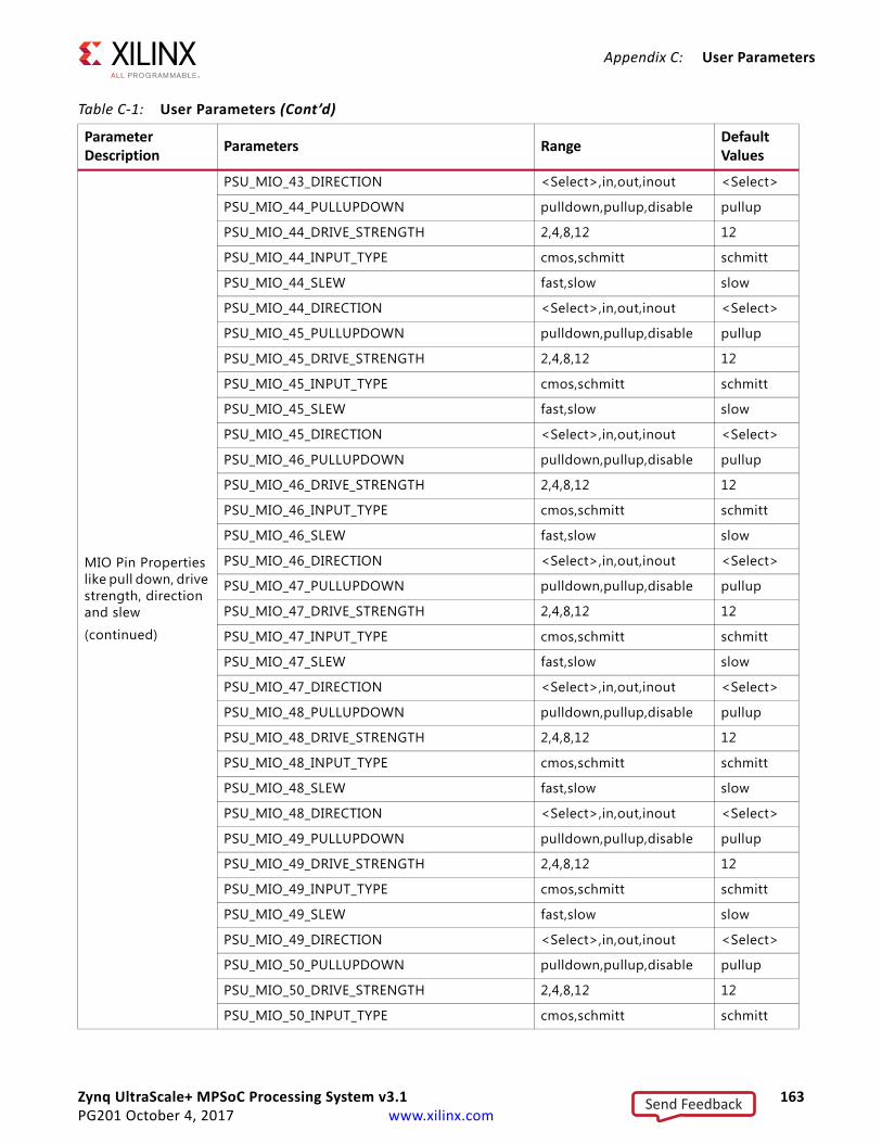
Zynq UltraScale+ MPSoC Processing System v3.1 163PG201 October 4, 2017 www.xilinx.com
Appendix C: User Parameters
MIO Pin Properties like pull down, drive strength, direction and slew
(continued)
PSU_MIO_43_DIRECTION <Select>,in,out,inout <Select>
PSU_MIO_44_PULLUPDOWN pulldown,pullup,disable pullup
PSU_MIO_44_DRIVE_STRENGTH 2,4,8,12 12
PSU_MIO_44_INPUT_TYPE cmos,schmitt schmitt
PSU_MIO_44_SLEW fast,slow slow
PSU_MIO_44_DIRECTION <Select>,in,out,inout <Select>
PSU_MIO_45_PULLUPDOWN pulldown,pullup,disable pullup
PSU_MIO_45_DRIVE_STRENGTH 2,4,8,12 12
PSU_MIO_45_INPUT_TYPE cmos,schmitt schmitt
PSU_MIO_45_SLEW fast,slow slow
PSU_MIO_45_DIRECTION <Select>,in,out,inout <Select>
PSU_MIO_46_PULLUPDOWN pulldown,pullup,disable pullup
PSU_MIO_46_DRIVE_STRENGTH 2,4,8,12 12
PSU_MIO_46_INPUT_TYPE cmos,schmitt schmitt
PSU_MIO_46_SLEW fast,slow slow
PSU_MIO_46_DIRECTION <Select>,in,out,inout <Select>
PSU_MIO_47_PULLUPDOWN pulldown,pullup,disable pullup
PSU_MIO_47_DRIVE_STRENGTH 2,4,8,12 12
PSU_MIO_47_INPUT_TYPE cmos,schmitt schmitt
PSU_MIO_47_SLEW fast,slow slow
PSU_MIO_47_DIRECTION <Select>,in,out,inout <Select>
PSU_MIO_48_PULLUPDOWN pulldown,pullup,disable pullup
PSU_MIO_48_DRIVE_STRENGTH 2,4,8,12 12
PSU_MIO_48_INPUT_TYPE cmos,schmitt schmitt
PSU_MIO_48_SLEW fast,slow slow
PSU_MIO_48_DIRECTION <Select>,in,out,inout <Select>
PSU_MIO_49_PULLUPDOWN pulldown,pullup,disable pullup
PSU_MIO_49_DRIVE_STRENGTH 2,4,8,12 12
PSU_MIO_49_INPUT_TYPE cmos,schmitt schmitt
PSU_MIO_49_SLEW fast,slow slow
PSU_MIO_49_DIRECTION <Select>,in,out,inout <Select>
PSU_MIO_50_PULLUPDOWN pulldown,pullup,disable pullup
PSU_MIO_50_DRIVE_STRENGTH 2,4,8,12 12
PSU_MIO_50_INPUT_TYPE cmos,schmitt schmitt
Table C‐1: User Parameters (Cont’d)
Parameter Description
Parameters RangeDefault Values
Send Feedback

Zynq UltraScale+ MPSoC Processing System v3.1 164PG201 October 4, 2017 www.xilinx.com
Appendix C: User Parameters
MIO Pin Properties like pull down, drive strength, direction and slew
(continued)
PSU_MIO_50_SLEW fast,slow slow
PSU_MIO_50_DIRECTION <Select>,in,out,inout <Select>
PSU_MIO_51_PULLUPDOWN pulldown,pullup,disable pullup
PSU_MIO_51_DRIVE_STRENGTH 2,4,8,12 12
PSU_MIO_51_INPUT_TYPE cmos,schmitt schmitt
PSU_MIO_51_SLEW fast,slow slow
PSU_MIO_51_DIRECTION <Select>,in,out,inout <Select>
PSU_MIO_52_PULLUPDOWN pulldown,pullup,disable pullup
PSU_MIO_52_DRIVE_STRENGTH 2,4,8,12 12
PSU_MIO_52_INPUT_TYPE cmos,schmitt schmitt
PSU_MIO_52_SLEW fast,slow slow
PSU_MIO_52_DIRECTION <Select>,in,out,inout <Select>
PSU_MIO_53_PULLUPDOWN pulldown,pullup,disable pullup
PSU_MIO_53_DRIVE_STRENGTH 2,4,8,12 12
PSU_MIO_53_INPUT_TYPE cmos,schmitt schmitt
PSU_MIO_53_SLEW fast,slow slow
PSU_MIO_53_DIRECTION <Select>,in,out,inout <Select>
PSU_MIO_54_PULLUPDOWN pulldown,pullup,disable pullup
PSU_MIO_54_DRIVE_STRENGTH 2,4,8,12 12
PSU_MIO_54_INPUT_TYPE cmos,schmitt schmitt
PSU_MIO_54_SLEW fast,slow slow
PSU_MIO_54_DIRECTION <Select>,in,out,inout <Select>
PSU_MIO_55_PULLUPDOWN pulldown,pullup,disable pullup
PSU_MIO_55_DRIVE_STRENGTH 2,4,8,12 12
PSU_MIO_55_INPUT_TYPE cmos,schmitt schmitt
PSU_MIO_55_SLEW fast,slow slow
PSU_MIO_55_DIRECTION <Select>,in,out,inout <Select>
PSU_MIO_56_PULLUPDOWN pulldown,pullup,disable pullup
PSU_MIO_56_DRIVE_STRENGTH 2,4,8,12 12
PSU_MIO_56_INPUT_TYPE cmos,schmitt schmitt
PSU_MIO_56_SLEW fast,slow slow
PSU_MIO_56_DIRECTION <Select>,in,out,inout <Select>
PSU_MIO_57_PULLUPDOWN pulldown,pullup,disable pullup
PSU_MIO_57_DRIVE_STRENGTH 2,4,8,12 12
Table C‐1: User Parameters (Cont’d)
Parameter Description
Parameters RangeDefault Values
Send Feedback

Zynq UltraScale+ MPSoC Processing System v3.1 165PG201 October 4, 2017 www.xilinx.com
Appendix C: User Parameters
MIO Pin Properties like pull down, drive strength, direction and slew
(continued)
PSU_MIO_57_INPUT_TYPE cmos,schmitt schmitt
PSU_MIO_57_SLEW fast,slow slow
PSU_MIO_57_DIRECTION <Select>,in,out,inout <Select>
PSU_MIO_58_PULLUPDOWN pulldown,pullup,disable pullup
PSU_MIO_58_DRIVE_STRENGTH 2,4,8,12 12
PSU_MIO_58_INPUT_TYPE cmos,schmitt schmitt
PSU_MIO_58_SLEW fast,slow slow
PSU_MIO_58_DIRECTION <Select>,in,out,inout <Select>
PSU_MIO_59_PULLUPDOWN pulldown,pullup,disable pullup
PSU_MIO_59_DRIVE_STRENGTH 2,4,8,12 12
PSU_MIO_59_INPUT_TYPE cmos,schmitt schmitt
PSU_MIO_59_SLEW fast,slow slow
PSU_MIO_59_DIRECTION <Select>,in,out,inout <Select>
PSU_MIO_60_PULLUPDOWN pulldown,pullup,disable pullup
PSU_MIO_60_DRIVE_STRENGTH 2,4,8,12 12
PSU_MIO_60_INPUT_TYPE cmos,schmitt schmitt
PSU_MIO_60_SLEW fast,slow slow
PSU_MIO_60_DIRECTION <Select>,in,out,inout <Select>
PSU_MIO_61_PULLUPDOWN pulldown,pullup,disable pullup
PSU_MIO_61_DRIVE_STRENGTH 2,4,8,12 12
PSU_MIO_61_INPUT_TYPE cmos,schmitt schmitt
PSU_MIO_61_SLEW fast,slow slow
PSU_MIO_61_DIRECTION <Select>,in,out,inout <Select>
PSU_MIO_62_PULLUPDOWN pulldown,pullup,disable pullup
PSU_MIO_62_DRIVE_STRENGTH 2,4,8,12 12
PSU_MIO_62_INPUT_TYPE cmos,schmitt schmitt
PSU_MIO_62_SLEW fast,slow slow
PSU_MIO_62_DIRECTION <Select>,in,out,inout <Select>
PSU_MIO_63_PULLUPDOWN pulldown,pullup,disable pullup
PSU_MIO_63_DRIVE_STRENGTH 2,4,8,12 12
PSU_MIO_63_INPUT_TYPE cmos,schmitt schmitt
PSU_MIO_63_SLEW fast,slow slow
PSU_MIO_63_DIRECTION <Select>,in,out,inout <Select>
PSU_MIO_64_PULLUPDOWN pulldown,pullup,disable pullup
Table C‐1: User Parameters (Cont’d)
Parameter Description
Parameters RangeDefault Values
Send Feedback

Zynq UltraScale+ MPSoC Processing System v3.1 166PG201 October 4, 2017 www.xilinx.com
Appendix C: User Parameters
MIO Pin Properties like pull down, drive strength, direction and slew
(continued)
PSU_MIO_64_DRIVE_STRENGTH 2,4,8,12 12
PSU_MIO_64_INPUT_TYPE cmos,schmitt schmitt
PSU_MIO_64_SLEW fast,slow slow
PSU_MIO_64_DIRECTION <Select>,in,out,inout <Select>
PSU_MIO_65_PULLUPDOWN pulldown,pullup,disable pullup
PSU_MIO_65_DRIVE_STRENGTH 2,4,8,12 12
PSU_MIO_65_INPUT_TYPE cmos,schmitt schmitt
PSU_MIO_65_SLEW fast,slow slow
PSU_MIO_65_DIRECTION <Select>,in,out,inout <Select>
PSU_MIO_66_PULLUPDOWN pulldown,pullup,disable pullup
PSU_MIO_66_DRIVE_STRENGTH 2,4,8,12 12
PSU_MIO_66_INPUT_TYPE cmos,schmitt schmitt
PSU_MIO_66_SLEW fast,slow slow
PSU_MIO_66_DIRECTION <Select>,in,out,inout <Select>
PSU_MIO_67_PULLUPDOWN pulldown,pullup,disable pullup
PSU_MIO_67_DRIVE_STRENGTH 2,4,8,12 12
PSU_MIO_67_INPUT_TYPE cmos,schmitt schmitt
PSU_MIO_67_SLEW fast,slow slow
PSU_MIO_67_DIRECTION <Select>,in,out,inout <Select>
PSU_MIO_68_PULLUPDOWN pulldown,pullup,disable pullup
PSU_MIO_68_DRIVE_STRENGTH 2,4,8,12 12
PSU_MIO_68_INPUT_TYPE cmos,schmitt schmitt
PSU_MIO_68_SLEW fast,slow slow
PSU_MIO_68_DIRECTION <Select>,in,out,inout <Select>
PSU_MIO_69_PULLUPDOWN pulldown,pullup,disable pullup
PSU_MIO_69_DRIVE_STRENGTH 2,4,8,12 12
PSU_MIO_69_INPUT_TYPE cmos,schmitt schmitt
PSU_MIO_69_SLEW fast,slow slow
PSU_MIO_69_DIRECTION <Select>,in,out,inout <Select>
PSU_MIO_70_PULLUPDOWN pulldown,pullup,disable pullup
PSU_MIO_70_DRIVE_STRENGTH 2,4,8,12 12
PSU_MIO_70_INPUT_TYPE cmos,schmitt schmitt
PSU_MIO_70_SLEW fast,slow slow
PSU_MIO_70_DIRECTION <Select>,in,out,inout <Select>
Table C‐1: User Parameters (Cont’d)
Parameter Description
Parameters RangeDefault Values
Send Feedback
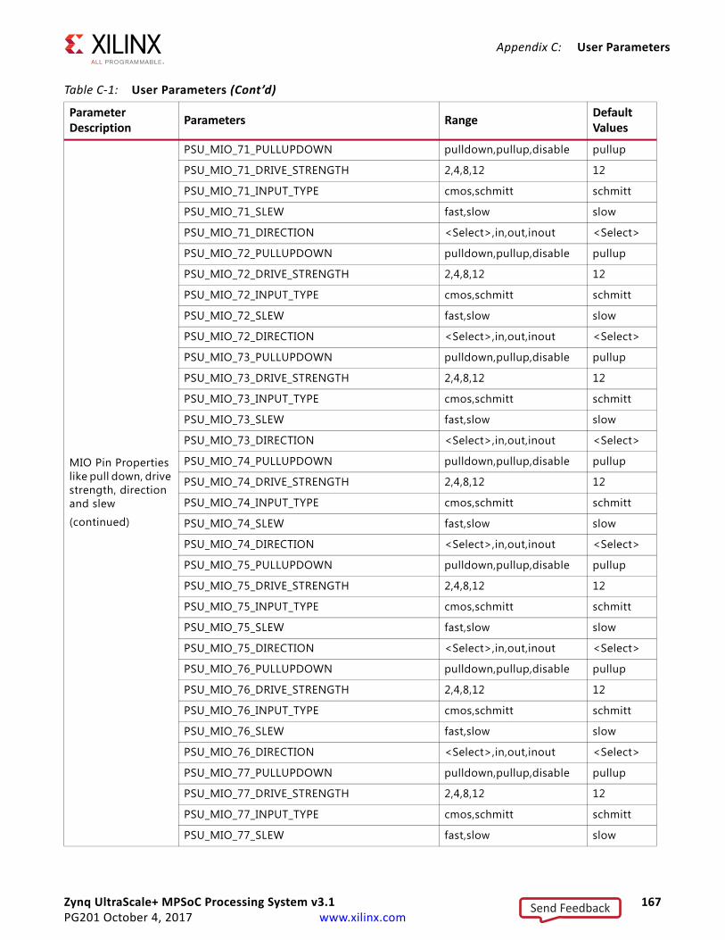
Zynq UltraScale+ MPSoC Processing System v3.1 167PG201 October 4, 2017 www.xilinx.com
Appendix C: User Parameters
MIO Pin Properties like pull down, drive strength, direction and slew
(continued)
PSU_MIO_71_PULLUPDOWN pulldown,pullup,disable pullup
PSU_MIO_71_DRIVE_STRENGTH 2,4,8,12 12
PSU_MIO_71_INPUT_TYPE cmos,schmitt schmitt
PSU_MIO_71_SLEW fast,slow slow
PSU_MIO_71_DIRECTION <Select>,in,out,inout <Select>
PSU_MIO_72_PULLUPDOWN pulldown,pullup,disable pullup
PSU_MIO_72_DRIVE_STRENGTH 2,4,8,12 12
PSU_MIO_72_INPUT_TYPE cmos,schmitt schmitt
PSU_MIO_72_SLEW fast,slow slow
PSU_MIO_72_DIRECTION <Select>,in,out,inout <Select>
PSU_MIO_73_PULLUPDOWN pulldown,pullup,disable pullup
PSU_MIO_73_DRIVE_STRENGTH 2,4,8,12 12
PSU_MIO_73_INPUT_TYPE cmos,schmitt schmitt
PSU_MIO_73_SLEW fast,slow slow
PSU_MIO_73_DIRECTION <Select>,in,out,inout <Select>
PSU_MIO_74_PULLUPDOWN pulldown,pullup,disable pullup
PSU_MIO_74_DRIVE_STRENGTH 2,4,8,12 12
PSU_MIO_74_INPUT_TYPE cmos,schmitt schmitt
PSU_MIO_74_SLEW fast,slow slow
PSU_MIO_74_DIRECTION <Select>,in,out,inout <Select>
PSU_MIO_75_PULLUPDOWN pulldown,pullup,disable pullup
PSU_MIO_75_DRIVE_STRENGTH 2,4,8,12 12
PSU_MIO_75_INPUT_TYPE cmos,schmitt schmitt
PSU_MIO_75_SLEW fast,slow slow
PSU_MIO_75_DIRECTION <Select>,in,out,inout <Select>
PSU_MIO_76_PULLUPDOWN pulldown,pullup,disable pullup
PSU_MIO_76_DRIVE_STRENGTH 2,4,8,12 12
PSU_MIO_76_INPUT_TYPE cmos,schmitt schmitt
PSU_MIO_76_SLEW fast,slow slow
PSU_MIO_76_DIRECTION <Select>,in,out,inout <Select>
PSU_MIO_77_PULLUPDOWN pulldown,pullup,disable pullup
PSU_MIO_77_DRIVE_STRENGTH 2,4,8,12 12
PSU_MIO_77_INPUT_TYPE cmos,schmitt schmitt
PSU_MIO_77_SLEW fast,slow slow
Table C‐1: User Parameters (Cont’d)
Parameter Description
Parameters RangeDefault Values
Send Feedback
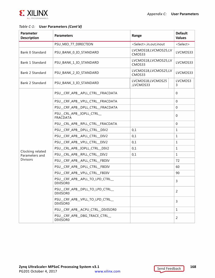
Zynq UltraScale+ MPSoC Processing System v3.1 168PG201 October 4, 2017 www.xilinx.com
Appendix C: User Parameters
PSU_MIO_77_DIRECTION <Select>,in,out,inout <Select>
Bank 0 Standard PSU_BANK_0_IO_STANDARD LVCMOS18,LVCMOS25,LVCMOS33 LVCMOS33
Bank 1 Standard PSU_BANK_1_IO_STANDARD LVCMOS18,LVCMOS25,LVCMOS33 LVCMOS33
Bank 2 Standard PSU_BANK_2_IO_STANDARD LVCMOS18,LVCMOS25,LVCMOS33 LVCMOS33
Bank 2 Standard PSU_BANK_3_IO_STANDARD LVCMOS18,LVCMOS25,LVCMOS33
LVCMOS33
Clocking related Parameters and Divisors
PSU__CRF_APB__APLL_CTRL__FRACDATA 0
PSU__CRF_APB__VPLL_CTRL__FRACDATA 0
PSU__CRF_APB__DPLL_CTRL__FRACDATA 0
PSU__CRL_APB__IOPLL_CTRL__FRACDATA 0
PSU__CRL_APB__RPLL_CTRL__FRACDATA 0
PSU__CRF_APB__DPLL_CTRL__DIV2 0,1 1
PSU__CRF_APB__APLL_CTRL__DIV2 0,1 1
PSU__CRF_APB__VPLL_CTRL__DIV2 0,1 1
PSU__CRL_APB__IOPLL_CTRL__DIV2 0,1 1
PSU__CRL_APB__RPLL_CTRL__DIV2 0,1 1
PSU__CRF_APB__APLL_CTRL__FBDIV 72
PSU__CRF_APB__DPLL_CTRL__FBDIV 60
PSU__CRF_APB__VPLL_CTRL__FBDIV 90
PSU__CRF_APB__APLL_TO_LPD_CTRL__DIVISOR0 3
PSU__CRF_APB__DPLL_TO_LPD_CTRL__DIVISOR0 2
PSU__CRF_APB__VPLL_TO_LPD_CTRL__DIVISOR0 3
PSU__CRF_APB__ACPU_CTRL__DIVISOR0 1
PSU__CRF_APB__DBG_TRACE_CTRL__DIVISOR0 2
Table C‐1: User Parameters (Cont’d)
Parameter Description
Parameters RangeDefault Values
Send Feedback

Zynq UltraScale+ MPSoC Processing System v3.1 169PG201 October 4, 2017 www.xilinx.com
Appendix C: User Parameters
Display Port
PSU__DISPLAYPORT__PERIPHERAL__ENABLE 0,1 0
PSU__DISPLAYPORT__LANE0__ENABLE 0,1 0
PSU__DISPLAYPORT__LANE0__IO <Select>,GT Lane1,GT Lane3 <Select>
PSU__DISPLAYPORT__LANE1__ENABLE 0,1 0
PSU__DISPLAYPORT__LANE1__IO <Select>,GT Lane0,GT Lane2 <Select>
Table C‐1: User Parameters (Cont’d)
Parameter Description
Parameters RangeDefault Values
Send Feedback
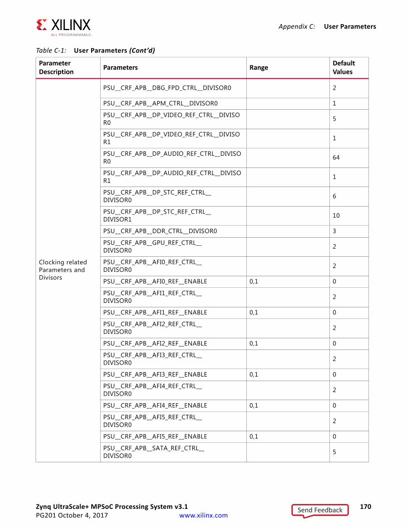
Zynq UltraScale+ MPSoC Processing System v3.1 170PG201 October 4, 2017 www.xilinx.com
Appendix C: User Parameters
Clocking related Parameters and Divisors
PSU__CRF_APB__DBG_FPD_CTRL__DIVISOR0 2
PSU__CRF_APB__APM_CTRL__DIVISOR0 1
PSU__CRF_APB__DP_VIDEO_REF_CTRL__DIVISOR0 5
PSU__CRF_APB__DP_VIDEO_REF_CTRL__DIVISOR1 1
PSU__CRF_APB__DP_AUDIO_REF_CTRL__DIVISOR0 64
PSU__CRF_APB__DP_AUDIO_REF_CTRL__DIVISOR1 1
PSU__CRF_APB__DP_STC_REF_CTRL__DIVISOR0 6
PSU__CRF_APB__DP_STC_REF_CTRL__DIVISOR1 10
PSU__CRF_APB__DDR_CTRL__DIVISOR0 3
PSU__CRF_APB__GPU_REF_CTRL__DIVISOR0 2
PSU__CRF_APB__AFI0_REF_CTRL__DIVISOR0 2
PSU__CRF_APB__AFI0_REF__ENABLE 0,1 0
PSU__CRF_APB__AFI1_REF_CTRL__DIVISOR0 2
PSU__CRF_APB__AFI1_REF__ENABLE 0,1 0
PSU__CRF_APB__AFI2_REF_CTRL__DIVISOR0 2
PSU__CRF_APB__AFI2_REF__ENABLE 0,1 0
PSU__CRF_APB__AFI3_REF_CTRL__DIVISOR0 2
PSU__CRF_APB__AFI3_REF__ENABLE 0,1 0
PSU__CRF_APB__AFI4_REF_CTRL__DIVISOR0 2
PSU__CRF_APB__AFI4_REF__ENABLE 0,1 0
PSU__CRF_APB__AFI5_REF_CTRL__DIVISOR0 2
PSU__CRF_APB__AFI5_REF__ENABLE 0,1 0
PSU__CRF_APB__SATA_REF_CTRL__DIVISOR0 5
Table C‐1: User Parameters (Cont’d)
Parameter Description
Parameters RangeDefault Values
Send Feedback

Zynq UltraScale+ MPSoC Processing System v3.1 171PG201 October 4, 2017 www.xilinx.com
Appendix C: User Parameters
SATA Related Parameters
PSU__SATA__PERIPHERAL__ENABLE 0,1 0
PSU__SATA__LANE0__ENABLE 0,1 0
PSU__SATA__LANE0__IO <Select>,GT Lane0,GT Lane2 <Select>
PSU__SATA__LANE1__ENABLE 0,1 0
PSU__SATA__LANE1__IO <Select>,GT Lane1,GT Lane3 <Select>
Clocking related Parameters and Divisors
PSU__CRF_APB__PCIE_REF_CTRL__DIVISOR0 6
PSU__CRL_APB__PL0_REF_CTRL__DIVISOR0 15
PSU__CRL_APB__PL1_REF_CTRL__DIVISOR0 4
PSU__CRL_APB__PL2_REF_CTRL__DIVISOR0 4
PSU__CRL_APB__PL3_REF_CTRL__DIVISOR0 4
PSU__CRL_APB__PL0_REF_CTRL__DIVISOR1 1
PSU__CRL_APB__PL1_REF_CTRL__DIVISOR1 1
PSU__CRL_APB__PL2_REF_CTRL__DIVISOR1 1
PSU__CRL_APB__PL3_REF_CTRL__DIVISOR1 1
PSU__CRL_APB__AMS_REF_CTRL__DIVISOR0 30
PSU__CRL_APB__AMS_REF_CTRL__DIVISOR1 1
PSU__CRL_APB__TIMESTAMP_REF_CTRL__DIVISOR0 15
PSU__CRL_APB__AFI6_REF_CTRL__DIVISOR0 3
PSU__CRL_APB__AFI6__ENABLE 0,1 0
PSU__CRL_APB__USB3_DUAL_REF_CTRL__DIVISOR0 5
PSU__CRL_APB__USB3_DUAL_REF_CTRL__DIVISOR1 15
PSU__CRL_APB__USB3__ENABLE 0,1 0
Table C‐1: User Parameters (Cont’d)
Parameter Description
Parameters RangeDefault Values
Send Feedback
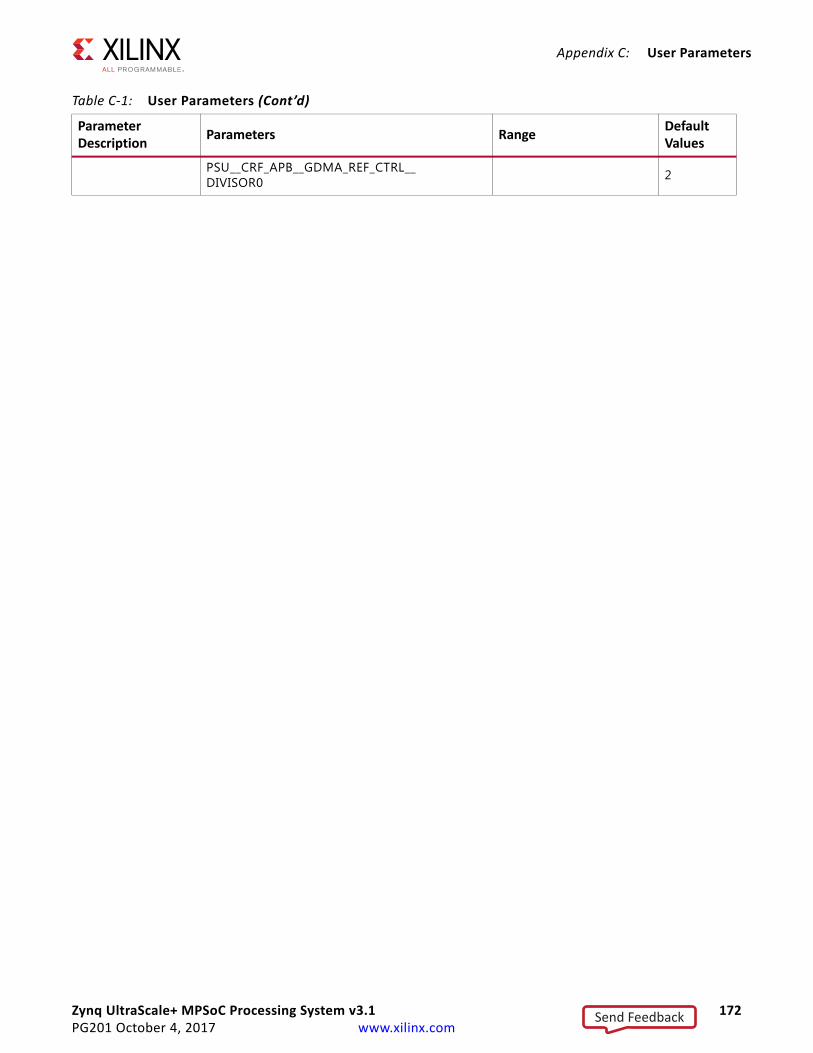
Zynq UltraScale+ MPSoC Processing System v3.1 172PG201 October 4, 2017 www.xilinx.com
Appendix C: User Parameters
PSU__CRF_APB__GDMA_REF_CTRL__DIVISOR0 2
Table C‐1: User Parameters (Cont’d)
Parameter Description
Parameters RangeDefault Values
Send Feedback

Zynq UltraScale+ MPSoC Processing System v3.1 173PG201 October 4, 2017 www.xilinx.com
Appendix C: User Parameters
Clocking related Parameters and Divisors
(continued)
PSU__CRF_APB__DPDMA_REF_CTRL__DIVISOR0 2
PSU__CRF_APB__TOPSW_MAIN_CTRL__DIVISOR0 2
PSU__CRF_APB__TOPSW_LSBUS_CTRL__DIVISOR0 5
PSU__CRF_APB__GTGREF0_REF_CTRL__DIVISOR0 -1
PSU__CRF_APB__GTGREF0__ENABLE NA NA
PSU__CRF_APB__DBG_TSTMP_CTRL__DIVISOR0 2
PSU__CRL_APB__IOPLL_CTRL__FBDIV 90
PSU__CRL_APB__RPLL_CTRL__FBDIV 90
PSU__CRL_APB__IOPLL_TO_FPD_CTRL__DIVISOR0 3
PSU__CRL_APB__RPLL_TO_FPD_CTRL__DIVISOR0 3
PSU__CRL_APB__GEM0_REF_CTRL__DIVISOR0 12
PSU__CRL_APB__GEM1_REF_CTRL__DIVISOR0 12
PSU__CRL_APB__GEM2_REF_CTRL__DIVISOR0 12
PSU__CRL_APB__GEM3_REF_CTRL__DIVISOR0 12
PSU__CRL_APB__GEM0_REF_CTRL__DIVISOR1 1
PSU__CRL_APB__GEM1_REF_CTRL__DIVISOR1 1
PSU__CRL_APB__GEM2_REF_CTRL__DIVISOR1 1
PSU__CRL_APB__GEM3_REF_CTRL__DIVISOR1 1
PSU__CRL_APB__GEM_TSU_REF_CTRL__DIVISOR0 4
PSU__CRL_APB__GEM_TSU_REF_CTRL__DIVISOR1 1
PSU__CRL_APB__USB0_BUS_REF_CTRL__DIVISOR0 6
Table C‐1: User Parameters (Cont’d)
Parameter Description
Parameters RangeDefault Values
Send Feedback
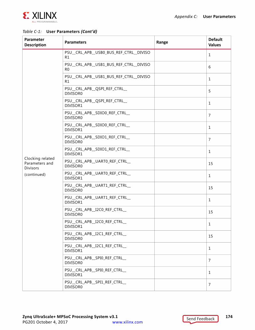
Zynq UltraScale+ MPSoC Processing System v3.1 174PG201 October 4, 2017 www.xilinx.com
Appendix C: User Parameters
Clocking related Parameters and Divisors
(continued)
PSU__CRL_APB__USB0_BUS_REF_CTRL__DIVISOR1 1
PSU__CRL_APB__USB1_BUS_REF_CTRL__DIVISOR0 6
PSU__CRL_APB__USB1_BUS_REF_CTRL__DIVISOR1 1
PSU__CRL_APB__QSPI_REF_CTRL__DIVISOR0 5
PSU__CRL_APB__QSPI_REF_CTRL__DIVISOR1 1
PSU__CRL_APB__SDIO0_REF_CTRL__DIVISOR0 7
PSU__CRL_APB__SDIO0_REF_CTRL__DIVISOR1 1
PSU__CRL_APB__SDIO1_REF_CTRL__DIVISOR0 7
PSU__CRL_APB__SDIO1_REF_CTRL__DIVISOR1 1
PSU__CRL_APB__UART0_REF_CTRL__DIVISOR0 15
PSU__CRL_APB__UART0_REF_CTRL__DIVISOR1 1
PSU__CRL_APB__UART1_REF_CTRL__DIVISOR0 15
PSU__CRL_APB__UART1_REF_CTRL__DIVISOR1 1
PSU__CRL_APB__I2C0_REF_CTRL__DIVISOR0 15
PSU__CRL_APB__I2C0_REF_CTRL__DIVISOR1 1
PSU__CRL_APB__I2C1_REF_CTRL__DIVISOR0 15
PSU__CRL_APB__I2C1_REF_CTRL__DIVISOR1 1
PSU__CRL_APB__SPI0_REF_CTRL__DIVISOR0 7
PSU__CRL_APB__SPI0_REF_CTRL__DIVISOR1 1
PSU__CRL_APB__SPI1_REF_CTRL__DIVISOR0 7
Table C‐1: User Parameters (Cont’d)
Parameter Description
Parameters RangeDefault Values
Send Feedback

Zynq UltraScale+ MPSoC Processing System v3.1 175PG201 October 4, 2017 www.xilinx.com
Appendix C: User Parameters
Clocking related Parameters and Divisors
(continued)
PSU__CRL_APB__SPI1_REF_CTRL__DIVISOR1 1
PSU__CRL_APB__CAN0_REF_CTRL__DIVISOR0 15
PSU__CRL_APB__CAN0_REF_CTRL__DIVISOR1 1
PSU__CRL_APB__CAN1_REF_CTRL__DIVISOR0 15
PSU__CRL_APB__CAN1_REF_CTRL__DIVISOR1 1
PSU__CRL_APB__DEBUG_R5_ATCLK_CTRL__DIVISOR0 6
PSU__CRL_APB__CPU_R5_CTRL__DIVISOR0 3
PSU__CRL_APB__OCM_MAIN_CTRL__DIVISOR0 3
PSU__CRL_APB__IOU_SWITCH_CTRL__DIVISOR0 6
PSU__CRL_APB__CSU_PLL_CTRL__DIVISOR0 3
PSU__CRL_APB__PCAP_CTRL__DIVISOR0 6
PSU__CRL_APB__LPD_LSBUS_CTRL__DIVISOR0 15
PSU__CRL_APB__LPD_SWITCH_CTRL__DIVISOR0 3
PSU__CRL_APB__DBG_LPD_CTRL__DIVISOR0 6
PSU__CRL_APB__NAND_REF_CTRL__DIVISOR0 15
PSU__CRL_APB__NAND_REF_CTRL__DIVISOR1 1
PSU__CRL_APB__ADMA_REF_CTRL__DIVISOR0 3
PSU__CRF_APB__APLL_CTRL__SRCSEL PSS_REF_CLK PSS_REF_CLK
PSU__CRF_APB__DPLL_CTRL__SRCSEL PSS_REF_CLK PSS_REF_CLK
PSU__CRF_APB__VPLL_CTRL__SRCSEL PSS_REF_CLK PSS_REF_CLK
PSU__CRF_APB__ACPU_CTRL__SRCSEL APLL,DPLL,VPLL APLL
Table C‐1: User Parameters (Cont’d)
Parameter Description
Parameters RangeDefault Values
Send Feedback
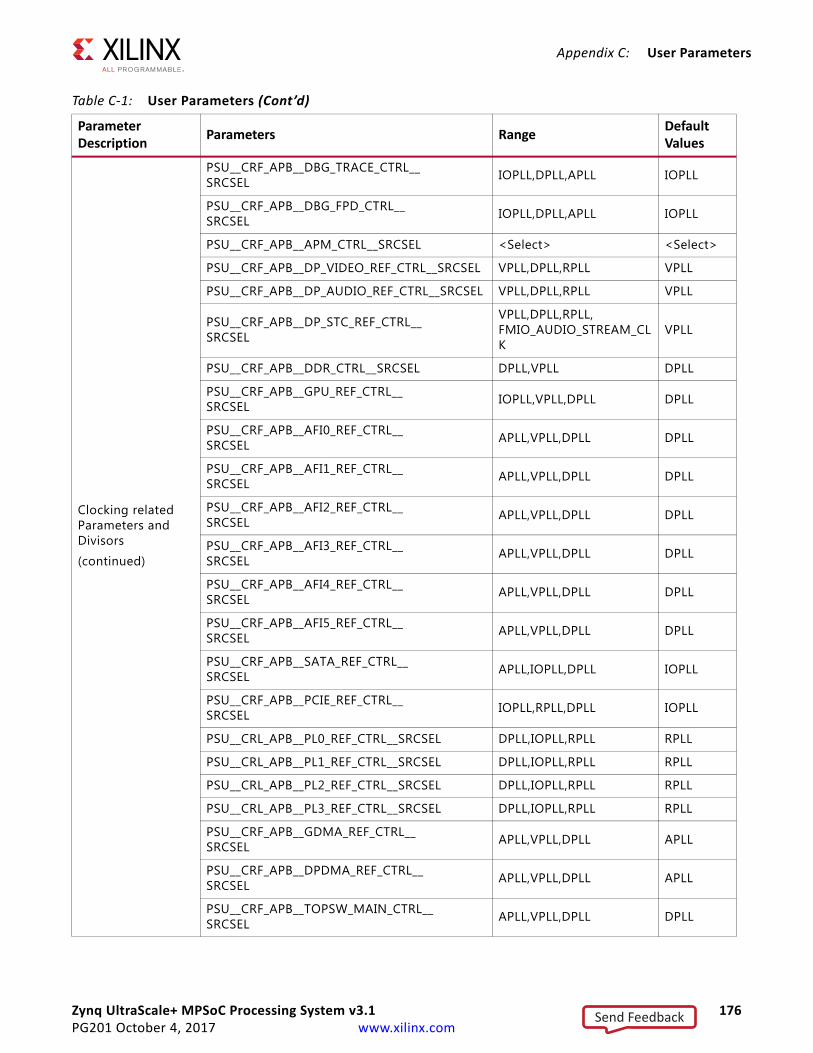
Zynq UltraScale+ MPSoC Processing System v3.1 176PG201 October 4, 2017 www.xilinx.com
Appendix C: User Parameters
Clocking related Parameters and Divisors
(continued)
PSU__CRF_APB__DBG_TRACE_CTRL__SRCSEL IOPLL,DPLL,APLL IOPLL
PSU__CRF_APB__DBG_FPD_CTRL__SRCSEL IOPLL,DPLL,APLL IOPLL
PSU__CRF_APB__APM_CTRL__SRCSEL <Select> <Select>
PSU__CRF_APB__DP_VIDEO_REF_CTRL__SRCSEL VPLL,DPLL,RPLL VPLL
PSU__CRF_APB__DP_AUDIO_REF_CTRL__SRCSEL VPLL,DPLL,RPLL VPLL
PSU__CRF_APB__DP_STC_REF_CTRL__SRCSEL
VPLL,DPLL,RPLL,FMIO_AUDIO_STREAM_CLK
VPLL
PSU__CRF_APB__DDR_CTRL__SRCSEL DPLL,VPLL DPLL
PSU__CRF_APB__GPU_REF_CTRL__SRCSEL IOPLL,VPLL,DPLL DPLL
PSU__CRF_APB__AFI0_REF_CTRL__SRCSEL APLL,VPLL,DPLL DPLL
PSU__CRF_APB__AFI1_REF_CTRL__SRCSEL APLL,VPLL,DPLL DPLL
PSU__CRF_APB__AFI2_REF_CTRL__SRCSEL APLL,VPLL,DPLL DPLL
PSU__CRF_APB__AFI3_REF_CTRL__SRCSEL APLL,VPLL,DPLL DPLL
PSU__CRF_APB__AFI4_REF_CTRL__SRCSEL APLL,VPLL,DPLL DPLL
PSU__CRF_APB__AFI5_REF_CTRL__SRCSEL APLL,VPLL,DPLL DPLL
PSU__CRF_APB__SATA_REF_CTRL__SRCSEL APLL,IOPLL,DPLL IOPLL
PSU__CRF_APB__PCIE_REF_CTRL__SRCSEL IOPLL,RPLL,DPLL IOPLL
PSU__CRL_APB__PL0_REF_CTRL__SRCSEL DPLL,IOPLL,RPLL RPLL
PSU__CRL_APB__PL1_REF_CTRL__SRCSEL DPLL,IOPLL,RPLL RPLL
PSU__CRL_APB__PL2_REF_CTRL__SRCSEL DPLL,IOPLL,RPLL RPLL
PSU__CRL_APB__PL3_REF_CTRL__SRCSEL DPLL,IOPLL,RPLL RPLL
PSU__CRF_APB__GDMA_REF_CTRL__SRCSEL APLL,VPLL,DPLL APLL
PSU__CRF_APB__DPDMA_REF_CTRL__SRCSEL APLL,VPLL,DPLL APLL
PSU__CRF_APB__TOPSW_MAIN_CTRL__SRCSEL APLL,VPLL,DPLL DPLL
Table C‐1: User Parameters (Cont’d)
Parameter Description
Parameters RangeDefault Values
Send Feedback
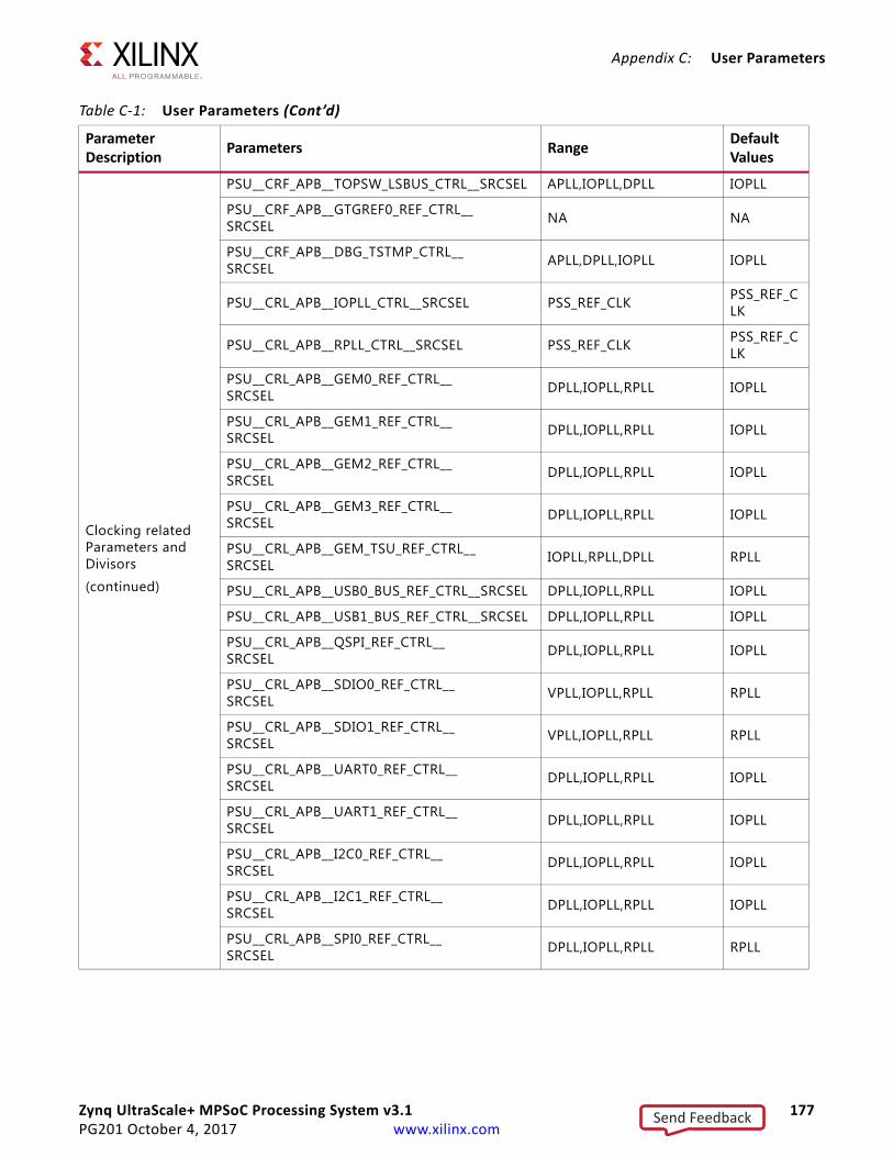
Zynq UltraScale+ MPSoC Processing System v3.1 177PG201 October 4, 2017 www.xilinx.com
Appendix C: User Parameters
Clocking related Parameters and Divisors
(continued)
PSU__CRF_APB__TOPSW_LSBUS_CTRL__SRCSEL APLL,IOPLL,DPLL IOPLL
PSU__CRF_APB__GTGREF0_REF_CTRL__SRCSEL NA NA
PSU__CRF_APB__DBG_TSTMP_CTRL__SRCSEL APLL,DPLL,IOPLL IOPLL
PSU__CRL_APB__IOPLL_CTRL__SRCSEL PSS_REF_CLK PSS_REF_CLK
PSU__CRL_APB__RPLL_CTRL__SRCSEL PSS_REF_CLK PSS_REF_CLK
PSU__CRL_APB__GEM0_REF_CTRL__SRCSEL DPLL,IOPLL,RPLL IOPLL
PSU__CRL_APB__GEM1_REF_CTRL__SRCSEL DPLL,IOPLL,RPLL IOPLL
PSU__CRL_APB__GEM2_REF_CTRL__SRCSEL DPLL,IOPLL,RPLL IOPLL
PSU__CRL_APB__GEM3_REF_CTRL__SRCSEL DPLL,IOPLL,RPLL IOPLL
PSU__CRL_APB__GEM_TSU_REF_CTRL__SRCSEL IOPLL,RPLL,DPLL RPLL
PSU__CRL_APB__USB0_BUS_REF_CTRL__SRCSEL DPLL,IOPLL,RPLL IOPLL
PSU__CRL_APB__USB1_BUS_REF_CTRL__SRCSEL DPLL,IOPLL,RPLL IOPLL
PSU__CRL_APB__QSPI_REF_CTRL__SRCSEL DPLL,IOPLL,RPLL IOPLL
PSU__CRL_APB__SDIO0_REF_CTRL__SRCSEL VPLL,IOPLL,RPLL RPLL
PSU__CRL_APB__SDIO1_REF_CTRL__SRCSEL VPLL,IOPLL,RPLL RPLL
PSU__CRL_APB__UART0_REF_CTRL__SRCSEL DPLL,IOPLL,RPLL IOPLL
PSU__CRL_APB__UART1_REF_CTRL__SRCSEL DPLL,IOPLL,RPLL IOPLL
PSU__CRL_APB__I2C0_REF_CTRL__SRCSEL DPLL,IOPLL,RPLL IOPLL
PSU__CRL_APB__I2C1_REF_CTRL__SRCSEL DPLL,IOPLL,RPLL IOPLL
PSU__CRL_APB__SPI0_REF_CTRL__SRCSEL DPLL,IOPLL,RPLL RPLL
Table C‐1: User Parameters (Cont’d)
Parameter Description
Parameters RangeDefault Values
Send Feedback
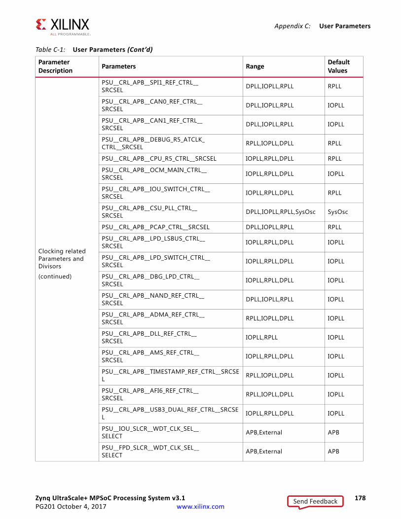
Zynq UltraScale+ MPSoC Processing System v3.1 178PG201 October 4, 2017 www.xilinx.com
Appendix C: User Parameters
Clocking related Parameters and Divisors
(continued)
PSU__CRL_APB__SPI1_REF_CTRL__SRCSEL DPLL,IOPLL,RPLL RPLL
PSU__CRL_APB__CAN0_REF_CTRL__SRCSEL DPLL,IOPLL,RPLL IOPLL
PSU__CRL_APB__CAN1_REF_CTRL__SRCSEL DPLL,IOPLL,RPLL IOPLL
PSU__CRL_APB__DEBUG_R5_ATCLK_CTRL__SRCSEL RPLL,IOPLL,DPLL RPLL
PSU__CRL_APB__CPU_R5_CTRL__SRCSEL IOPLL,RPLL,DPLL RPLL
PSU__CRL_APB__OCM_MAIN_CTRL__SRCSEL IOPLL,RPLL,DPLL IOPLL
PSU__CRL_APB__IOU_SWITCH_CTRL__SRCSEL IOPLL,RPLL,DPLL RPLL
PSU__CRL_APB__CSU_PLL_CTRL__SRCSEL DPLL,IOPLL,RPLL,SysOsc SysOsc
PSU__CRL_APB__PCAP_CTRL__SRCSEL DPLL,IOPLL,RPLL RPLL
PSU__CRL_APB__LPD_LSBUS_CTRL__SRCSEL IOPLL,RPLL,DPLL IOPLL
PSU__CRL_APB__LPD_SWITCH_CTRL__SRCSEL IOPLL,RPLL,DPLL IOPLL
PSU__CRL_APB__DBG_LPD_CTRL__SRCSEL IOPLL,RPLL,DPLL IOPLL
PSU__CRL_APB__NAND_REF_CTRL__SRCSEL DPLL,IOPLL,RPLL IOPLL
PSU__CRL_APB__ADMA_REF_CTRL__SRCSEL RPLL,IOPLL,DPLL IOPLL
PSU__CRL_APB__DLL_REF_CTRL__SRCSEL IOPLL,RPLL IOPLL
PSU__CRL_APB__AMS_REF_CTRL__SRCSEL IOPLL,RPLL,DPLL IOPLL
PSU__CRL_APB__TIMESTAMP_REF_CTRL__SRCSEL RPLL,IOPLL,DPLL IOPLL
PSU__CRL_APB__AFI6_REF_CTRL__SRCSEL RPLL,IOPLL,DPLL IOPLL
PSU__CRL_APB__USB3_DUAL_REF_CTRL__SRCSEL IOPLL,RPLL,DPLL IOPLL
PSU__IOU_SLCR__WDT_CLK_SEL__SELECT APB,External APB
PSU__FPD_SLCR__WDT_CLK_SEL__SELECT APB,External APB
Table C‐1: User Parameters (Cont’d)
Parameter Description
Parameters RangeDefault Values
Send Feedback

Zynq UltraScale+ MPSoC Processing System v3.1 179PG201 October 4, 2017 www.xilinx.com
Appendix C: User Parameters
Clocking related Parameters and Divisors
(continued)
PSU__IOU_SLCR__IOU_TTC_APB_CLK__TTC0_SEL APB,CPU_R5,PSS_REF_CLK APB
PSU__IOU_SLCR__IOU_TTC_APB_CLK__TTC1_SEL APB,CPU_R5,PSS_REF_CLK APB
PSU__IOU_SLCR__IOU_TTC_APB_CLK__TTC2_SEL APB,CPU_R5,PSS_REF_CLK APB
PSU__IOU_SLCR__IOU_TTC_APB_CLK__TTC3_SEL APB,CPU_R5,PSS_REF_CLK APB
PSU__CRF_APB__APLL_FRAC_CFG__ENABLED 0,1 0
PSU__CRF_APB__VPLL_FRAC_CFG__ENABLED 0,1 0
PSU__CRF_APB__DPLL_FRAC_CFG__ENABLED 0,1 0
PSU__CRL_APB__IOPLL_FRAC_CFG__ENABLED 0,1 0
PSU__CRL_APB__RPLL_FRAC_CFG__ENABLED 0,1 0
PSU__OVERRIDE__BASIC_CLOCK 0,1 0
PSU__PL_CLK0_BUF FALSE,TRUE TRUE
PSU__PL_CLK1_BUF FALSE,TRUE FALSE
PSU__PL_CLK2_BUF FALSE,TRUE FALSE
PSU__PL_CLK3_BUF FALSE,TRUE FALSE
PSU__CRF_APB__APLL_CTRL__FRACFREQ 27.138
PSU__CRF_APB__VPLL_CTRL__FRACFREQ 27.138
PSU__CRF_APB__DPLL_CTRL__FRACFREQ 27.138
PSU__CRL_APB__IOPLL_CTRL__FRACFREQ 27.138
PSU__CRL_APB__RPLL_CTRL__FRACFREQ 27.138
PSU__IOU_SLCR__TTC0__ACT_FREQMHZ 0.000000,600.000000 100
PSU__IOU_SLCR__TTC1__ACT_FREQMHZ 0.000000,600.000000 100
PSU__IOU_SLCR__TTC2__ACT_FREQMHZ 0.000000,600.000000 100
PSU__IOU_SLCR__TTC3__ACT_FREQMHZ 600.000000,0.000000 100
PSU__IOU_SLCR__WDT0__ACT_FREQMHZ 0.000000,100.000000 100
PSU__FPD_SLCR__WDT1__ACT_FREQMHZ 100
Table C‐1: User Parameters (Cont’d)
Parameter Description
Parameters RangeDefault Values
Send Feedback

Zynq UltraScale+ MPSoC Processing System v3.1 180PG201 October 4, 2017 www.xilinx.com
Appendix C: User Parameters
Clocking related Parameters and Divisors
(continued)
PSU__CRF_APB__ACPU_CTRL__ACT_FREQMHZ 1199.988
PSU__CRF_APB__DBG_TRACE_CTRL__ACT_FREQMHZ 249.997
PSU__CRF_APB__DBG_FPD_CTRL__ACT_FREQMHZ 249.997
PSU__CRF_APB__APM_CTRL__ACT_FREQMHZ 1
PSU__CRF_APB__DP_VIDEO_REF_CTRL__ACT_FREQMHZ 320
PSU__CRF_APB__DP_AUDIO_REF_CTRL__ACT_FREQMHZ 25
PSU__CRF_APB__DP_STC_REF_CTRL__ACT_FREQMHZ 27
PSU__CRF_APB__DDR_CTRL__ACT_FREQMHZ 374.996
PSU__DDR__INTERFACE__FREQMHZ 0.000000,600.000000 400.00
PSU__CRF_APB__GPU_REF_CTRL__ACT_FREQMHZ 499.995
PSU__CRF_APB__AFI0_REF_CTRL__ACT_FREQMHZ 667
PSU__CRF_APB__AFI1_REF_CTRL__ACT_FREQMHZ 667
PSU__CRF_APB__AFI2_REF_CTRL__ACT_FREQMHZ 667
PSU__CRF_APB__AFI3_REF_CTRL__ACT_FREQMHZ 667
PSU__CRF_APB__AFI4_REF_CTRL__ACT_FREQMHZ 667
PSU__CRF_APB__AFI5_REF_CTRL__ACT_FREQMHZ 667
PSU__CRF_APB__SATA_REF_CTRL__ACT_FREQMHZ 250
PSU__CRF_APB__PCIE_REF_CTRL__ACT_FREQMHZ 250
PSU__CRL_APB__PL0_REF_CTRL__ACT_FREQMHZ 99.999
PSU__CRL_APB__PL1_REF_CTRL__ACT_FREQMHZ 100
PSU__CRL_APB__PL2_REF_CTRL__ACT_FREQMHZ 100
Table C‐1: User Parameters (Cont’d)
Parameter Description
Parameters RangeDefault Values
Send Feedback
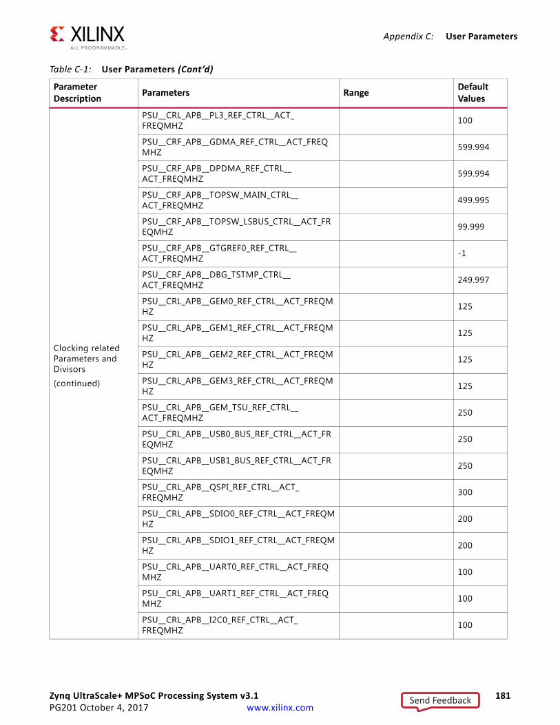
Zynq UltraScale+ MPSoC Processing System v3.1 181PG201 October 4, 2017 www.xilinx.com
Appendix C: User Parameters
Clocking related Parameters and Divisors
(continued)
PSU__CRL_APB__PL3_REF_CTRL__ACT_FREQMHZ 100
PSU__CRF_APB__GDMA_REF_CTRL__ACT_FREQMHZ 599.994
PSU__CRF_APB__DPDMA_REF_CTRL__ACT_FREQMHZ 599.994
PSU__CRF_APB__TOPSW_MAIN_CTRL__ACT_FREQMHZ 499.995
PSU__CRF_APB__TOPSW_LSBUS_CTRL__ACT_FREQMHZ 99.999
PSU__CRF_APB__GTGREF0_REF_CTRL__ACT_FREQMHZ -1
PSU__CRF_APB__DBG_TSTMP_CTRL__ACT_FREQMHZ 249.997
PSU__CRL_APB__GEM0_REF_CTRL__ACT_FREQMHZ 125
PSU__CRL_APB__GEM1_REF_CTRL__ACT_FREQMHZ 125
PSU__CRL_APB__GEM2_REF_CTRL__ACT_FREQMHZ 125
PSU__CRL_APB__GEM3_REF_CTRL__ACT_FREQMHZ 125
PSU__CRL_APB__GEM_TSU_REF_CTRL__ACT_FREQMHZ 250
PSU__CRL_APB__USB0_BUS_REF_CTRL__ACT_FREQMHZ 250
PSU__CRL_APB__USB1_BUS_REF_CTRL__ACT_FREQMHZ 250
PSU__CRL_APB__QSPI_REF_CTRL__ACT_FREQMHZ 300
PSU__CRL_APB__SDIO0_REF_CTRL__ACT_FREQMHZ 200
PSU__CRL_APB__SDIO1_REF_CTRL__ACT_FREQMHZ 200
PSU__CRL_APB__UART0_REF_CTRL__ACT_FREQMHZ 100
PSU__CRL_APB__UART1_REF_CTRL__ACT_FREQMHZ 100
PSU__CRL_APB__I2C0_REF_CTRL__ACT_FREQMHZ 100
Table C‐1: User Parameters (Cont’d)
Parameter Description
Parameters RangeDefault Values
Send Feedback
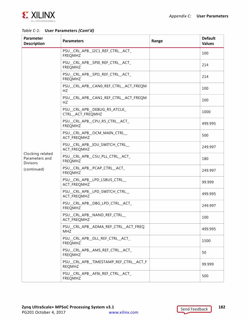
Zynq UltraScale+ MPSoC Processing System v3.1 182PG201 October 4, 2017 www.xilinx.com
Appendix C: User Parameters
Clocking related Parameters and Divisors
(continued)
PSU__CRL_APB__I2C1_REF_CTRL__ACT_FREQMHZ 100
PSU__CRL_APB__SPI0_REF_CTRL__ACT_FREQMHZ 214
PSU__CRL_APB__SPI1_REF_CTRL__ACT_FREQMHZ 214
PSU__CRL_APB__CAN0_REF_CTRL__ACT_FREQMHZ 100
PSU__CRL_APB__CAN1_REF_CTRL__ACT_FREQMHZ 100
PSU__CRL_APB__DEBUG_R5_ATCLK_CTRL__ACT_FREQMHZ 1000
PSU__CRL_APB__CPU_R5_CTRL__ACT_FREQMHZ 499.995
PSU__CRL_APB__OCM_MAIN_CTRL__ACT_FREQMHZ 500
PSU__CRL_APB__IOU_SWITCH_CTRL__ACT_FREQMHZ 249.997
PSU__CRL_APB__CSU_PLL_CTRL__ACT_FREQMHZ 180
PSU__CRL_APB__PCAP_CTRL__ACT_FREQMHZ 249.997
PSU__CRL_APB__LPD_LSBUS_CTRL__ACT_FREQMHZ 99.999
PSU__CRL_APB__LPD_SWITCH_CTRL__ACT_FREQMHZ 499.995
PSU__CRL_APB__DBG_LPD_CTRL__ACT_FREQMHZ 249.997
PSU__CRL_APB__NAND_REF_CTRL__ACT_FREQMHZ 100
PSU__CRL_APB__ADMA_REF_CTRL__ACT_FREQMHZ 499.995
PSU__CRL_APB__DLL_REF_CTRL__ACT_FREQMHZ 1500
PSU__CRL_APB__AMS_REF_CTRL__ACT_FREQMHZ 50
PSU__CRL_APB__TIMESTAMP_REF_CTRL__ACT_FREQMHZ 99.999
PSU__CRL_APB__AFI6_REF_CTRL__ACT_FREQMHZ 500
Table C‐1: User Parameters (Cont’d)
Parameter Description
Parameters RangeDefault Values
Send Feedback

Zynq UltraScale+ MPSoC Processing System v3.1 183PG201 October 4, 2017 www.xilinx.com
Appendix C: User Parameters
Clocking related Parameters and Divisors
(continued)
PSU__CRL_APB__USB3_DUAL_REF_CTRL__ACT_FREQMHZ 20
PSU__CRF_APB__ACPU_CTRL__FREQMHZ 0.000000,1500.000000 1200
PSU__CRF_APB__DBG_TRACE_CTRL__FREQMHZ 0.000000,250.000000 250
PSU__CRF_APB__DBG_FPD_CTRL__FREQMHZ 0.000000,250.000000 250
PSU__CRF_APB__APM_CTRL__FREQMHZ -2,-1 1
PSU__CRF_APB__DP_VIDEO_REF_CTRL__FREQMHZ 0.000000,320.000000 320
PSU__CRF_APB__DP_AUDIO_REF_CTRL__FREQMHZ 0.000000,25.000000 25
PSU__CRF_APB__DP_STC_REF_CTRL__FREQMHZ 0.000000,27.000000 27
PSU__CRF_APB__DDR_CTRL__FREQMHZ 100.000000,667.000000 800
PSU__CRF_APB__GPU_REF_CTRL__FREQMHZ 0.000000,667.000000 500
PSU__CRF_APB__AFI0_REF_CTRL__FREQMHZ 0.000000,667.000000 667
PSU__CRF_APB__AFI1_REF_CTRL__FREQMHZ 0.000000,667.000000 667
PSU__CRF_APB__AFI2_REF_CTRL__FREQMHZ 0.000000,667.000000 667
PSU__CRF_APB__AFI3_REF_CTRL__FREQMHZ 0.000000,667.000000 667
PSU__CRF_APB__AFI4_REF_CTRL__FREQMHZ 0.000000,667.000000 667
PSU__CRF_APB__AFI5_REF_CTRL__FREQMHZ 0.000000,667.000000 667
PSU__CRF_APB__SATA_REF_CTRL__FREQMHZ 0.000000,250.000000 250
PSU__CRF_APB__PCIE_REF_CTRL__FREQMHZ 0.000000,250.000000 250
PSU__CRL_APB__PL0_REF_CTRL__FREQMHZ 0.000000,400.000000 100
PSU__CRL_APB__PL1_REF_CTRL__FREQMHZ 0.000000,400.000000 100
PSU__CRL_APB__PL2_REF_CTRL__FREQMHZ 0.000000,400.000000 100
Table C‐1: User Parameters (Cont’d)
Parameter Description
Parameters RangeDefault Values
Send Feedback

Zynq UltraScale+ MPSoC Processing System v3.1 184PG201 October 4, 2017 www.xilinx.com
Appendix C: User Parameters
Clocking related Parameters and Divisors
(continued)
PSU__CRL_APB__PL3_REF_CTRL__FREQMHZ 0.000000,400.000000 100
PSU__CRF_APB__GDMA_REF_CTRL__FREQMHZ 0.000000,667.000000 600
PSU__CRF_APB__DPDMA_REF_CTRL__FREQMHZ 0.000000,667.000000 600
PSU__CRF_APB__TOPSW_MAIN_CTRL__FREQMHZ 0.000000,600.000000 533.33
PSU__CRF_APB__TOPSW_LSBUS_CTRL__FREQMHZ 0.000000,100.000000 100
PSU__CRF_APB__GTGREF0_REF_CTRL__FREQMHZ -2,-1 -1
PSU__CRF_APB__DBG_TSTMP_CTRL__FREQMHZ 0.000000,250.000000 250
PSU__CRL_APB__GEM0_REF_CTRL__FREQMHZ 0.000000,125.000000 125
PSU__CRL_APB__GEM1_REF_CTRL__FREQMHZ 0.000000,125.000000 125
PSU__CRL_APB__GEM2_REF_CTRL__FREQMHZ 0.000000,125.000000 125
PSU__CRL_APB__GEM3_REF_CTRL__FREQMHZ 0.000000,125.000000 125
PSU__CRL_APB__GEM_TSU_REF_CTRL__FREQMHZ 0.000000,250.000000 250
PSU__CRL_APB__USB0_BUS_REF_CTRL__FREQMHZ 0.000000,250.000000 250
PSU__CRL_APB__USB1_BUS_REF_CTRL__FREQMHZ 0.000000,250.000000 250
PSU__CRL_APB__QSPI_REF_CTRL__FREQMHZ 0.000000,300.000000 300
PSU__CRL_APB__SDIO0_REF_CTRL__FREQMHZ 0.000000,200.000000 200
PSU__CRL_APB__SDIO1_REF_CTRL__FREQMHZ 0.000000,200.000000 200
PSU__CRL_APB__UART0_REF_CTRL__FREQMHZ 0.000000,100.000000 100
PSU__CRL_APB__UART1_REF_CTRL__FREQMHZ 0.000000,100.000000 100
PSU__CRL_APB__I2C0_REF_CTRL__FREQMHZ 0.000000,100.000000 100
Table C‐1: User Parameters (Cont’d)
Parameter Description
Parameters RangeDefault Values
Send Feedback

Zynq UltraScale+ MPSoC Processing System v3.1 185PG201 October 4, 2017 www.xilinx.com
Appendix C: User Parameters
Clocking related Parameters and Divisors
(continued)
PSU__CRL_APB__I2C1_REF_CTRL__FREQMHZ 0.000000,100.000000 100
PSU__CRL_APB__SPI0_REF_CTRL__FREQMHZ 0.000000,200.000000 200
PSU__CRL_APB__SPI1_REF_CTRL__FREQMHZ 0.000000,200.000000 200
PSU__CRL_APB__CAN0_REF_CTRL__FREQMHZ 0.000000,100.000000 100
PSU__CRL_APB__CAN1_REF_CTRL__FREQMHZ 0.000000,100.000000 100
PSU__CRL_APB__DEBUG_R5_ATCLK_CTRL__FREQMHZ 0.000000,1000.000000 1000
PSU__CRL_APB__CPU_R5_CTRL__FREQMHZ 0.000000,600.000000 500
PSU__CRL_APB__OCM_MAIN_CTRL__FREQMHZ 0.000000,600.000000 500
PSU__CRL_APB__IOU_SWITCH_CTRL__FREQMHZ 0.000000,267.000000 267
PSU__CRL_APB__CSU_PLL_CTRL__FREQMHZ 0.000000,400.000000 180
PSU__CRL_APB__PCAP_CTRL__FREQMHZ 0.000000,250.000000 250
PSU__CRL_APB__LPD_LSBUS_CTRL__FREQMHZ 0.000000,100.000000 100
PSU__CRL_APB__LPD_SWITCH_CTRL__FREQMHZ 0.000000,600.000000 500
PSU__CRL_APB__DBG_LPD_CTRL__FREQMHZ 0.000000,267.000000 250
PSU__CRL_APB__NAND_REF_CTRL__FREQMHZ 0.000000,100.000000 100
PSU__CRL_APB__ADMA_REF_CTRL__FREQMHZ 0.000000,600.000000 500
PSU__CRL_APB__DLL_REF_CTRL__FREQMHZ 0.000000,1500.000000 1500
PSU__CRL_APB__AMS_REF_CTRL__FREQMHZ 0.000000,52.000000 50
PSU__CRL_APB__TIMESTAMP_REF_CTRL__FREQMHZ 0.000000,100.000000 100
PSU__CRL_APB__AFI6_REF_CTRL__FREQMHZ 0.000000,600.000000 500
PSU__CRL_APB__USB3_DUAL_REF_CTRL_FREQMHZ 0.000000,20.000000 20
Table C‐1: User Parameters (Cont’d)
Parameter Description
Parameters RangeDefault Values
Send Feedback
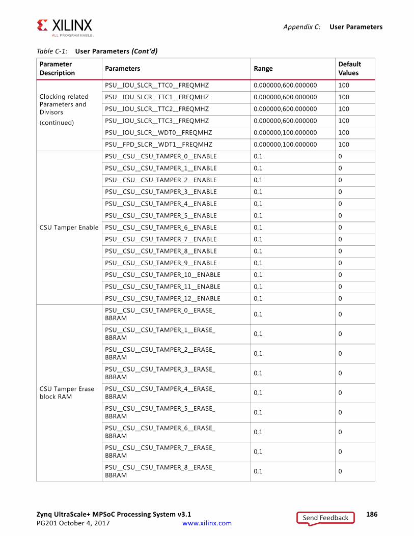
Zynq UltraScale+ MPSoC Processing System v3.1 186PG201 October 4, 2017 www.xilinx.com
Appendix C: User Parameters
Clocking related Parameters and Divisors
(continued)
PSU__IOU_SLCR__TTC0__FREQMHZ 0.000000,600.000000 100
PSU__IOU_SLCR__TTC1__FREQMHZ 0.000000,600.000000 100
PSU__IOU_SLCR__TTC2__FREQMHZ 0.000000,600.000000 100
PSU__IOU_SLCR__TTC3__FREQMHZ 0.000000,600.000000 100
PSU__IOU_SLCR__WDT0__FREQMHZ 0.000000,100.000000 100
PSU__FPD_SLCR__WDT1__FREQMHZ 0.000000,100.000000 100
CSU Tamper Enable
PSU__CSU__CSU_TAMPER_0__ENABLE 0,1 0
PSU__CSU__CSU_TAMPER_1__ENABLE 0,1 0
PSU__CSU__CSU_TAMPER_2__ENABLE 0,1 0
PSU__CSU__CSU_TAMPER_3__ENABLE 0,1 0
PSU__CSU__CSU_TAMPER_4__ENABLE 0,1 0
PSU__CSU__CSU_TAMPER_5__ENABLE 0,1 0
PSU__CSU__CSU_TAMPER_6__ENABLE 0,1 0
PSU__CSU__CSU_TAMPER_7__ENABLE 0,1 0
PSU__CSU__CSU_TAMPER_8__ENABLE 0,1 0
PSU__CSU__CSU_TAMPER_9__ENABLE 0,1 0
PSU__CSU__CSU_TAMPER_10__ENABLE 0,1 0
PSU__CSU__CSU_TAMPER_11__ENABLE 0,1 0
PSU__CSU__CSU_TAMPER_12__ENABLE 0,1 0
CSU Tamper Erase block RAM
PSU__CSU__CSU_TAMPER_0__ERASE_BBRAM 0,1 0
PSU__CSU__CSU_TAMPER_1__ERASE_BBRAM 0,1 0
PSU__CSU__CSU_TAMPER_2__ERASE_BBRAM 0,1 0
PSU__CSU__CSU_TAMPER_3__ERASE_BBRAM 0,1 0
PSU__CSU__CSU_TAMPER_4__ERASE_BBRAM 0,1 0
PSU__CSU__CSU_TAMPER_5__ERASE_BBRAM 0,1 0
PSU__CSU__CSU_TAMPER_6__ERASE_BBRAM 0,1 0
PSU__CSU__CSU_TAMPER_7__ERASE_BBRAM 0,1 0
PSU__CSU__CSU_TAMPER_8__ERASE_BBRAM 0,1 0
Table C‐1: User Parameters (Cont’d)
Parameter Description
Parameters RangeDefault Values
Send Feedback

Zynq UltraScale+ MPSoC Processing System v3.1 187PG201 October 4, 2017 www.xilinx.com
Appendix C: User Parameters
CSU Tamper Erase block RAM
(continued)
PSU__CSU__CSU_TAMPER_9__ERASE_BBRAM 0,1 0
PSU__CSU__CSU_TAMPER_10__ERASE_BBRAM 0,1 0
PSU__CSU__CSU_TAMPER_11__ERASE_BBRAM 0,1 0
PSU__CSU__CSU_TAMPER_12__ERASE_BBRAM 0,1 0
Table C‐1: User Parameters (Cont’d)
Parameter Description
Parameters RangeDefault Values
Send Feedback
Zynq UltraScale+ MPSoC Processing System v3.1 188PG201 October 4, 2017 www.xilinx.com
Appendix C: User Parameters
CSU Tamper Response
PSU__CSU__CSU_TAMPER_0__RESPONSE
<Select>,SEC_LOCKDOWN_0,SEC_LOCKDOWN_1,SYS_RESET,SYS_INTERRUPT
<Select>
PSU__CSU__CSU_TAMPER_1__RESPONSE
<Select>,SEC_LOCKDOWN_0,SEC_LOCKDOWN_1,SYS_RESET,SYS_INTERRUPT
<Select>
PSU__CSU__CSU_TAMPER_2__RESPONSE
<Select>,SEC_LOCKDOWN_0,SEC_LOCKDOWN_1,SYS_RESET,SYS_INTERRUPT
<Select>
PSU__CSU__CSU_TAMPER_3__RESPONSE
<Select>,SEC_LOCKDOWN_0,SEC_LOCKDOWN_1,SYS_RESET,SYS_INTERRUPT
<Select>
PSU__CSU__CSU_TAMPER_4__RESPONSE
<Select>,SEC_LOCKDOWN_0,SEC_LOCKDOWN_1,SYS_RESET,SYS_INTERRUPT
<Select>
PSU__CSU__CSU_TAMPER_5__RESPONSE
<Select>,SEC_LOCKDOWN_0,SEC_LOCKDOWN_1,SYS_RESET,SYS_INTERRUPT
<Select>
PSU__CSU__CSU_TAMPER_6__RESPONSE
<Select>,SEC_LOCKDOWN_0,SEC_LOCKDOWN_1,SYS_RESET,SYS_INTERRUPT
<Select>
PSU__CSU__CSU_TAMPER_7__RESPONSE
<Select>,SEC_LOCKDOWN_0,SEC_LOCKDOWN_1,SYS_RESET,SYS_INTERRUPT
<Select>
PSU__CSU__CSU_TAMPER_8__RESPONSE
<Select>,SEC_LOCKDOWN_0,SEC_LOCKDOWN_1,SYS_RESET,SYS_INTERRUPT
<Select>
PSU__CSU__CSU_TAMPER_9__RESPONSE
<Select>,SEC_LOCKDOWN_0,SEC_LOCKDOWN_1,SYS_RESET,SYS_INTERRUPT
<Select>
Table C‐1: User Parameters (Cont’d)
Parameter Description
Parameters RangeDefault Values
Send Feedback

Zynq UltraScale+ MPSoC Processing System v3.1 189PG201 October 4, 2017 www.xilinx.com
Appendix C: User Parameters
CSU Tamper Response
(continued)
PSU__CSU__CSU_TAMPER_12__RESPONSE
<Select>,SEC_LOCKDOWN_0,SEC_LOCKDOWN_1,SYS_RESET,SYS_INTERRUPT
<Select>
PSU__GEN_IPI_0__MASTER
NONE,APU,RPU0,RPU1,S_AXI_HP1_FPD,S_AXI_HP2_FPD,S_AXI_HP3_FPD,S_AXI_LPD, S_AXI_HP0_FPD, S_AXI_HPC0_FPD,S_AXI_HPC1_FPD, S_AXI_ACP_FPD
APU
PSU__GEN_IPI_1__MASTER
NONE,APU,RPU0,RPU1,S_AXI_HP1_FPD,S_AXI_HP2_FPD,S_AXI_HP3_FPD,S_AXI_LPD, S_AXI_HP0_FPD, S_AXI_HPC0_FPD,S_AXI_HPC1_FPD, S_AXI_ACP_FPD
RPU0
PSU__GEN_IPI_2__MASTER
NONE,APU,RPU0,RPU1,S_AXI_HP1_FPD,S_AXI_HP2_FPD,S_AXI_HP3_FPD,S_AXI_LPD, S_AXI_HP0_FPD, S_AXI_HPC0_FPD,S_AXI_HPC1_FPD, S_AXI_ACP_FPD
RPU1
PSU__GEN_IPI_3__MASTER NONE,PMU PMU
PSU__GEN_IPI_4__MASTER NONE,PMU PMU
PSU__GEN_IPI_5__MASTER NONE,PMU PMU
IPI Master PSU__GEN_IPI_6__MASTER NONE,PMU PMU
PSU__GEN_IPI_7__MASTER
NONE,APU,RPU0,RPU1,S_AXI_HP1_FPD,S_AXI_HP2_FPD,S_AXI_HP3_FPD,S_AXI_LPD, S_AXI_HP0_FPD, S_AXI_HPC0_FPD,S_AXI_HPC1_FPD, S_AXI_ACP_FPD
NONE
PSU__GEN_IPI_8__MASTER
NONE,APU,RPU0,RPU1,S_AXI_HP1_FPD,S_AXI_HP2_FPD,S_AXI_HP3_FPD,S_AXI_LPD, S_AXI_HP0_FPD, S_AXI_HPC0_FPD,S_AXI_HPC1_FPD, S_AXI_ACP_FPD
NONE
Table C‐1: User Parameters (Cont’d)
Parameter Description
Parameters RangeDefault Values
Send Feedback
Zynq UltraScale+ MPSoC Processing System v3.1 190PG201 October 4, 2017 www.xilinx.com
Appendix C: User Parameters
PSU__GEN_IPI_9__MASTER
NONE,APU,RPU0,RPU1,S_AXI_HP1_FPD,S_AXI_HP2_FPD,S_AXI_HP3_FPD,S_AXI_LPD, S_AXI_HP0_FPD, S_AXI_HPC0_FPD,S_AXI_HPC1_FPD, S_AXI_ACP_FPD
NONE
Table C‐1: User Parameters (Cont’d)
Parameter Description
Parameters RangeDefault Values
Send Feedback

Zynq UltraScale+ MPSoC Processing System v3.1 191PG201 October 4, 2017 www.xilinx.com
Appendix C: User Parameters
PSU__GEN_IPI_10__MASTER
NONE,APU,RPU0,RPU1,S_AXI_HP1_FPD,S_AXI_HP2_FPD,S_AXI_HP3_FPD,S_AXI_LPD, S_AXI_HP0_FPD, S_AXI_HPC0_FPD,S_AXI_HPC1_FPD, S_AXI_ACP_FPD
NONE
PSU__NUM_FABRIC_RESETS 0,1,2,3,4 1
PSU__GPIO_EMIO__WIDTH NA [94:0]
PSU__REPORT__DBGLOG 0,1 0
Notes: 1. Reserve, Wireless controller, Satellite communication controller, Data acquisition and signal processing controllers,
Intelligent I/O controllers, Docking stations, Device was built before Class Code definitions were finalized, Memory controller, Simple communication controller, Serial bus controllers, Encryption/Decryption controller, Display controller, Multimedia device, Input devices, Mass storage controller, Processors, Device does not fit in any defined classes, Bridge device, Network controller, Base system peripherals, Multimedia device
2. ADMA is also referenced as LPD_DMA throughout this guide. These two terms are synonymous.3. GDMA is also referenced as FPD_DMA throughout this guide. These two terms are synonymous.
Table C‐1: User Parameters (Cont’d)
Parameter Description
Parameters RangeDefault Values
Table C‐2: PSU__PROTECTION__MASTERS Default Values
Default Values
USB1:NonSecure;0 USB0:NonSecure;0 S_AXI_LPD:NA;0
S_AXI_HPC1_FPD:NA;0 S_AXI_HPC0_FPD:NA;0 S_AXI_HP3_FPD:NA;0
S_AXI_HP2_FPD:NA;0 S_AXI_HP1_FPD:NA;0 S_AXI_HP0_FPD:NA;0
S_AXI_ACP:NA;0 S_AXI_ACE:NA;0 SD1:Secure;0
SD0:Secure;0 SATA1:NonSecure;0 SATA0:NonSecure;0
RPU1:Secure;1 RPU0:Secure;1 QSPI:Secure;0
PMU:NA;1 PCIe:NonSecure;0 NAND:Secure;0
LDMA:NA;1 GPU:Secure;1 GEM3:Secure;0
GEM2:Secure;0 GEM1:Secure;0 GEM0:Secure;0
FDMA:NA;1 DP:NonSecure;0 DAP:NA;1’
Coresight:NA;1 CSU:NA;1 APU:NA;1
Send Feedback

Appendix C: User Parameters
Zynq UltraScale+ MPSoC Processing System v3.1 192PG201 October 4, 2017 www.xilinx.com
Table C‐3: PSU__PROTECTION__SLAVES
Default Values
LPD;USB3_1_XHCI;FE300000;FE3FFFFF;0 LPD;USB3_1;FF9E0000;FF9EFFFF;0 LPD;USB3_0_XHCI;FE200000;FE2FFFFF;0
LPD;USB3_0;FF9D0000;FF9DFFFF;0 LPD;UART1;FF010000;FF01FFFF;0 LPD;UART0;FF000000;FF00FFFF;0
LPD;TTC3;FF140000;FF14FFFF;0 LPD;TTC2;FF130000;FF13FFFF;0 LPD;TTC1;FF120000;FF12FFFF;0
LPD;TTC0;FF110000;FF11FFFF;0 FPD;SWDT1;FD4D0000;FD4DFFFF;0 LPD;SWDT0;FF150000;FF15FFFF;0
LPD;SPI1;FF050000;FF05FFFF;0 LPD;SPI0;FF040000;FF04FFFF;0 FPD;SMMU_REG;FD5F0000;FD5FFFFF;1
FPD;SMMU;FD800000;FDFFFFFF;1 FPD;SIOU;FD3D0000;FD3DFFFF;1 FPD;SERDES;FD400000;FD47FFFF;1
LPD;SD1;FF170000;FF17FFFF;0 LPD;SD0;FF160000;FF16FFFF;0 FPD;SATA;FD0C0000;FD0CFFFF;0
LPD;RTC;FFA60000;FFA6FFFF;1 LPD;RSA_CORE;FFCE0000;FFCEFFFF;1 LPD;RPU;FF9A0000;FF9AFFFF;1
FPD;RCPU_GIC;F9000000;F900FFFF;1
LPD;R5_TCM_RAM_GLOBAL;FFE00000;FFE3FFF
F;1
LPD;R5_1_Instruction_Cache;FFEC0000;FFECFFFF;
1
LPD;R5_1_Data_Cache;FFED0000;FFEDFFFF;1
LPD;R5_1_BTCM_GLOBAL;FFEB0000;FFEBFFFF;
1 LPD;R5_1_ATCM_GLOBAL;FFE90000;FFE9FFFF;1
LPD;R5_0_Instruction_Cache;FFE40000;FFE4FFF
F;1 LPD;R5_0_Data_Cache;FFE50000;FFE5FFFF;1 LPD;R5_0_BTCM_GLOBAL;FFE20000;FFE2FFFF;1
LPD;R5_0_ATCM_GLOBAL;FFE00000;FFE0FFFF;1
LPD;QSPI_Linear_Address;C0000000;DFFFFFFF;
1 LPD;QSPI;FF0F0000;FF0FFFFF;0
LPD;PMU_RAM;FFDC0000;FFDDFFFF;1 LPD;PMU_GLOBAL;FFD80000;FFDBFFFF;1 FPD;PCIE_MAIN;FD0E0000;FD0EFFFF;0
FPD;PCIE_LOW;E0000000;EFFFFFFF;0 FPD;PCIE_HIGH;600000000;7FFFFFFFF;0 FPD;PCIE_DMA;FD0F0000;FD0FFFFF;0
FPD;PCIE_ATTRIB;FD480000;FD48FFFF;0 LPD;OCM_XMPU_CFG;FFA70000;FFA7FFFF;1 LPD;OCM_SLCR;FF960000;FF96FFFF;1
OCM;OCM;FFFC0000;FFFFFFFF;1 LPD;NAND;FF100000;FF10FFFF;0 LPD;MBISTJTAG;FFCF0000;FFCFFFFF;1
LPD;LPD_XPPU_SINK;FF9C0000;FF9CFFFF;1 LPD;LPD_XPPU;FF980000;FF98FFFF;1 LPD;LPD_SLCR_SECURE;FF4B0000;FF4DFFFF;1
LPD;LPD_SLCR;FF410000;FF4AFFFF;1 LPD;LPD_GPV;FE100000;FE1FFFFF;1 LPD;LPD_DMA_7;FFAF0000;FFAFFFFF;1
LPD;LPD_DMA_6;FFAE0000;FFAEFFFF;1 LPD;LPD_DMA_5;FFAD0000;FFADFFFF;1 LPD;LPD_DMA_4;FFAC0000;FFACFFFF;1
LPD;LPD_DMA_3;FFAB0000;FFABFFFF;1 LPD;LPD_DMA_2;FFAA0000;FFAAFFFF;1 LPD;LPD_DMA_1;FFA90000;FFA9FFFF;1
LPD;LPD_DMA_0;FFA80000;FFA8FFFF;1 LPD;IPI_CTRL;FF380000;FF3FFFFF;1 LPD;IOU_SLCR;FF180000;FF23FFFF;1

Appendix C: User Parameters
Zynq UltraScale+ MPSoC Processing System v3.1 193PG201 October 4, 2017 www.xilinx.com
LPD;IOU_SECURE_SLCR;FF240000;FF24FFFF;1 LPD;IOU_SCNTRS;FF260000;FF26FFFF;1 LPD;IOU_SCNTR;FF250000;FF25FFFF;1
LPD;IOU_GPV;FE000000;FE0FFFFF;1 LPD;I2C1;FF030000;FF03FFFF;0 LPD;I2C0;FF020000;FF02FFFF;0
FPD;GPU;FD4B0000;FD4BFFFF;1 LPD;GPIO;FF0A0000;FF0AFFFF;1 LPD;GEM3;FF0E0000;FF0EFFFF;0
LPD;GEM2;FF0D0000;FF0DFFFF;0 LPD;GEM1;FF0C0000;FF0CFFFF;0 LPD;GEM0;FF0B0000;FF0BFFFF;0
FPD;FPD_XMPU_SINK;FD4F0000;FD4FFFFF;1 FPD;FPD_XMPU_CFG;FD5D0000;FD5DFFFF;1 FPD;FPD_SLCR_SECURE;FD690000;FD6CFFFF;1
FPD;FPD_SLCR;FD610000;FD68FFFF;1 FPD;FPD_GPV;FD700000;FD7FFFFF;1 FPD;FPD_DMA_CH7;FD570000;FD57FFFF;1
FPD;FPD_DMA_CH6;FD560000;FD56FFFF;1 FPD;FPD_DMA_CH5;FD550000;FD55FFFF;1 FPD;FPD_DMA_CH4;FD540000;FD54FFFF;1
FPD;FPD_DMA_CH3;FD530000;FD53FFFF;1 FPD;FPD_DMA_CH2;FD520000;FD52FFFF;1 FPD;FPD_DMA_CH1;FD510000;FD51FFFF;1
FPD;FPD_DMA_CH0;FD500000;FD50FFFF;1 LPD;EFUSE;FFCC0000;FFCCFFFF;1 FPD;Display Port;FD4A0000;FD4AFFFF;0
FPD;DPDMA;FD4C0000;FD4CFFFF;1 FPD;DDR_XMPU5_CFG;FD050000;FD05FFFF;1 FPD;DDR_XMPU4_CFG;FD040000;FD04FFFF;1
FPD;DDR_XMPU3_CFG;FD030000;FD03FFFF;1 FPD;DDR_XMPU2_CFG;FD020000;FD02FFFF;1 FPD;DDR_XMPU1_CFG;FD010000;FD01FFFF;1
FPD;DDR_XMPU0_CFG;FD000000;FD00FFFF;1 FPD;DDR_QOS_CTRL;FD090000;FD09FFFF;1 FPD;DDR_PHY;FD080000;FD08FFFF;1
DDR;DDR_LOW;0;7FFFFFFF;1 DDR;DDR_HIGH;800000000;800000000;0 FPD;DDDR_CTRL;FD070000;FD070FFF;1
LPD;Coresight;FE800000;FEFFFFFF;1 LPD;CSU_DMA;FFC80000;FFC9FFFF;1 LPD;CSU;FFCA0000;FFCAFFFF;0
LPD;CRL_APB;FF5E0000;FF85FFFF;1 FPD;CRF_APB;FD1A0000;FD2DFFFF;1 FPD;CCI_REG;FD5E0000;FD5EFFFF;1
FPD;CCI_GPV;FD6E0000;FD6EFFFF;1 LPD;CAN1;FF070000;FF07FFFF;0 LPD;CAN0;FF060000;FF06FFFF;0
FPD;APU;FD5C0000;FD5CFFFF;1 LPD;APM_INTC_IOU;FFA20000;FFA2FFFF;1 LPD;APM_FPD_LPD;FFA30000;FFA3FFFF;1
FPD;APM_5;FD490000;FD49FFFF;1 FPD;APM_0;FD0B0000;FD0BFFFF;1 LPD;APM2;FFA10000;FFA1FFFF;1
LPD;APM1;FFA00000;FFA0FFFF;1 LPD;AMS;FFA50000;FFA5FFFF;1 FPD;AFI_5;FD3B0000;FD3BFFFF;1
FPD;AFI_4;FD3A0000;FD3AFFFF;1 FPD;AFI_3;FD390000;FD39FFFF;1 FPD;AFI_2;FD380000;FD38FFFF;1
FPD;AFI_1;FD370000;FD37FFFF;1 FPD;AFI_0;FD360000;FD36FFFF;1 LPD;AFIFM6;FF9B0000;FF9BFFFF;1
FPD;ACPU_GIC;F9000000;F907FFFF;1
Table C‐3: PSU__PROTECTION__SLAVES (Cont’d)
Default Values
Zynq UltraScale+ MPSoC Processing System v3.1 194PG201 October 4, 2017 www.xilinx.com
Appendix D
DebuggingThis appendix includes details about resources available on the Xilinx Support website and debugging tools.
Finding Help on Xilinx.comTo help in the design and debug process when using the Zynq® UltraScale+™ MPSoC Processing System, the Xilinx Support web page contains key resources such as product documentation, release notes, answer records, information about known issues, and links for obtaining further product support.
DocumentationThis product guide is the main document associated with the core. This guide, along with documentation related to all products that aid in the design process, can be found on the Xilinx Support web page or by using the Xilinx® Documentation Navigator.
Download the Xilinx Documentation Navigator from the Downloads page. For more information about this tool and the features available, open the online help after installation.
Solution CentersSee the Xilinx Solution Centers for support on devices, software tools, and intellectual property at all stages of the design cycle. Topics include design assistance, advisories, and troubleshooting tips.
Send Feedback

Zynq UltraScale+ MPSoC Processing System v3.1 195PG201 October 4, 2017 www.xilinx.com
Appendix D: Debugging
Answer RecordsAnswer Records include information about commonly encountered problems, helpful information on how to resolve these problems, and any known issues with a Xilinx product. Answer Records are created and maintained daily ensuring that users have access to the most accurate information available.
Answer Records for this core can also be located by using the Search Support box on the main Xilinx support web page. To maximize your search results, use proper keywords such as
• Product name
• Tool message(s)
• Summary of the issue encountered
A filter search is available after results are returned to further target the results.
Master Answer Record for the Zynq UltraScale MPSoC Processing System
AR: 66183
Technical SupportXilinx provides technical support at the Xilinx Support web page for this LogiCORE™ IP product when used as described in the product documentation. Xilinx cannot guarantee timing, functionality, or support if you do any of the following:
• Implement the solution in devices that are not defined in the documentation.
• Customize the solution beyond that allowed in the product documentation.
• Change any section of the design labeled DO NOT MODIFY.
To contact Xilinx Technical Support, navigate to the Xilinx Support web page.
Send Feedback

Zynq UltraScale+ MPSoC Processing System v3.1 196PG201 October 4, 2017 www.xilinx.com
Appendix E
Additional Resources and Legal Notices
Xilinx ResourcesFor support resources such as Answers, Documentation, Downloads, and Forums, see Xilinx Support.
Documentation Navigator and Design HubsXilinx® Documentation Navigator provides access to Xilinx documents, videos, and support resources, which you can filter and search to find information. To open the Xilinx Documentation Navigator (DocNav):
• From the Vivado® IDE, select Help > Documentation and Tutorials.
• On Windows, select Start > All Programs > Xilinx Design Tools > DocNav.
• At the Linux command prompt, enter docnav.
Xilinx® Design Hubs provide links to documentation organized by design tasks and other topics, which you can use to learn key concepts and address frequently asked questions. To access the Design Hubs:
• In the Xilinx Documentation Navigator, click the Design Hubs View tab.
• On the Xilinx website, see the Design Hubs page.
Note: For more information on Documentation Navigator, see the Documentation Navigator page on the Xilinx website.
Send Feedback

Zynq UltraScale+ MPSoC Processing System v3.1 197PG201 October 4, 2017 www.xilinx.com
Appendix E: Additional Resources and Legal Notices
ReferencesThese documents provide supplemental material useful with this product guide:
1. Zynq UltraScale All Programmable MPSoC Technical Reference Manual (UG1085)
2. Zynq UltraScale+ MPSoC Register Reference (UG1087)
3. Vivado Design Suite User Guide: Designing IP Subsystems using IP Integrator (UG994)
4. Vivado Design Suite User Guide: Designing with IP (UG896)
5. Vivado Design Suite User Guide: Getting Started (UG910)
6. Vivado Design Suite User Guide: Programming and Debugging (UG908)
7. AMBA AXI4-Stream Protocol Specification
8. DDR3L SDRAM Data Sheet (PDF location -- Micron Technology Inc.)
9. UltraScale Devices Gen3 Integrated Block for PCI Express LogiCORE IP Product Guide (PG156)
10. Zynq UltraScale+ All Programmable MPSoC Verification IP Data Sheet (DS941)
Send Feedback
Zynq UltraScale+ MPSoC Processing System v3.1 198PG201 October 4, 2017 www.xilinx.com
Appendix E: Additional Resources and Legal Notices
Revision HistoryThe following table shows the revision history for this document.
Date Version Revision
10/04/2017 3.1
• Updated signal range for signal Number 1 in Table 2-2.
• Updated signals in Connectivity section in Chapter 2.
• Added Fractional Clocking and Load DDR Presets sections to Chapter 4.
• Updated Speed Bin option in DDR Memory Options in Chapter 4.
• Updated Figures 4-1, 4-7, 4-9, and 4-10.
• Added ten new options to the Other Options section in Chapter 4.
• Updated Notice of Disclaimer and added Automotive Applications Disclaimer.
• Added Preset Support section to Chapter 4.
• Added new table for TSU signals in Appendix B.
• Removed CONFIG. from several of the Parameters in Table C-1.
• Removed SME parameters from Table C-1.
04/05/2017 3.0
• Updated all the PCW screens as per the new look and feel changes in current Vivado IDE.
• Updated Isolation settings configuration information in Chapter 4.
• Updated clocking details of Output Clocks section in Chapter 4.
• LPD_DMA (ADMA) and FPD_DMA(GDMA) signal names have been standardized across the guide.
11/30/20162.0
• Updated Figure 4-7 and Figure 5-1.
• Removed ECC Scrub from page 35.
• Added I/O Configuration table to Appendix D, Port Descriptions.
• Changed many port names in Appendix B, Port Descriptions. See Appendix A, Migrating and Updating for details.
10/05/2016 2.0
• Added Updated all screen displays in Chapter 4.
• Updated the GT Lane clocking description in Chapter 4.
• Updated most of the DDR Configuration section in Chapter 4.
• Added the PCIe Configuration and Isolation Configurations in PCW sections in Chapter 4.
• Replaced User Parameters table in Appendix C.
Send Feedback
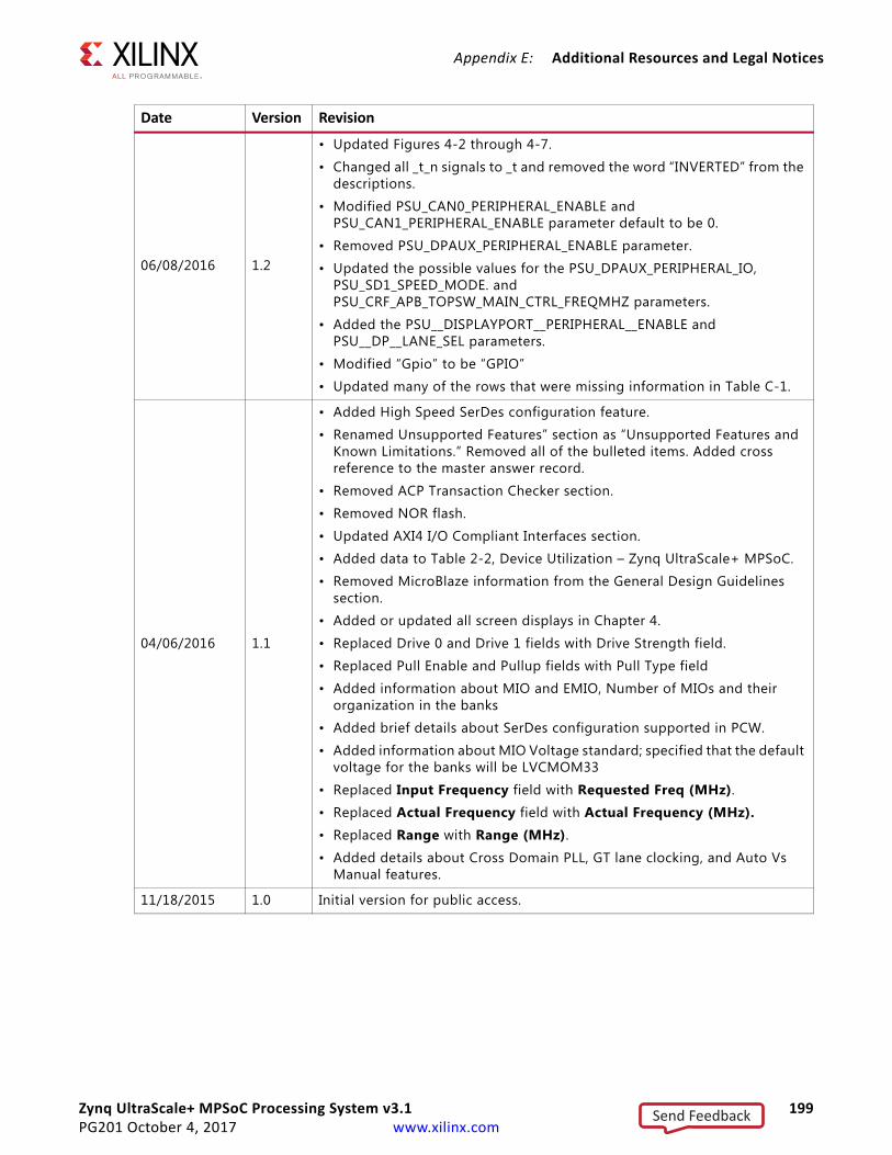
Zynq UltraScale+ MPSoC Processing System v3.1 199PG201 October 4, 2017 www.xilinx.com
Appendix E: Additional Resources and Legal Notices
06/08/2016 1.2
• Updated Figures 4-2 through 4-7.
• Changed all _t_n signals to _t and removed the word “INVERTED” from the descriptions.
• Modified PSU_CAN0_PERIPHERAL_ENABLE and PSU_CAN1_PERIPHERAL_ENABLE parameter default to be 0.
• Removed PSU_DPAUX_PERIPHERAL_ENABLE parameter.
• Updated the possible values for the PSU_DPAUX_PERIPHERAL_IO, PSU_SD1_SPEED_MODE. and PSU_CRF_APB_TOPSW_MAIN_CTRL_FREQMHZ parameters.
• Added the PSU__DISPLAYPORT__PERIPHERAL__ENABLE and PSU__DP__LANE_SEL parameters.
• Modified “Gpio” to be “GPIO”
• Updated many of the rows that were missing information in Table C-1.
04/06/2016 1.1
• Added High Speed SerDes configuration feature.
• Renamed Unsupported Features” section as “Unsupported Features and Known Limitations.” Removed all of the bulleted items. Added cross reference to the master answer record.
• Removed ACP Transaction Checker section.
• Removed NOR flash.
• Updated AXI4 I/O Compliant Interfaces section.
• Added data to Table 2-2, Device Utilization – Zynq UltraScale+ MPSoC.
• Removed MicroBlaze information from the General Design Guidelines section.
• Added or updated all screen displays in Chapter 4.
• Replaced Drive 0 and Drive 1 fields with Drive Strength field.
• Replaced Pull Enable and Pullup fields with Pull Type field
• Added information about MIO and EMIO, Number of MIOs and their organization in the banks
• Added brief details about SerDes configuration supported in PCW.
• Added information about MIO Voltage standard; specified that the default voltage for the banks will be LVCMOM33
• Replaced Input Frequency field with Requested Freq (MHz).• Replaced Actual Frequency field with Actual Frequency (MHz).• Replaced Range with Range (MHz).• Added details about Cross Domain PLL, GT lane clocking, and Auto Vs
Manual features.
11/18/2015 1.0 Initial version for public access.
Date Version Revision
Send Feedback
Zynq UltraScale+ MPSoC Processing System v3.1 200PG201 October 4, 2017 www.xilinx.com
Appendix E: Additional Resources and Legal Notices
Notice of DisclaimerThe information disclosed to you hereunder (the “Materials”) is provided solely for the selection and use of Xilinx products. To the maximum extent permitted by applicable law: (1) Materials are made available "AS IS" and with all faults, Xilinx hereby DISCLAIMS ALL WARRANTIES AND CONDITIONS, EXPRESS, IMPLIED, OR STATUTORY, INCLUDING BUT NOT LIMITED TO WARRANTIES OF MERCHANTABILITY, NON-INFRINGEMENT, OR FITNESS FOR ANY PARTICULAR PURPOSE; and (2) Xilinx shall not be liable (whether in contract or tort, including negligence, or under any other theory of liability) for any loss or damage of any kind or nature related to, arising under, or in connection with, the Materials (including your use of the Materials), including for any direct, indirect, special, incidental, or consequential loss or damage (including loss of data, profits, goodwill, or any type of loss or damage suffered as a result of any action brought by a third party) even if such damage or loss was reasonably foreseeable or Xilinx had been advised of the possibility of the same. Xilinx assumes no obligation to correct any errors contained in the Materials or to notify you of updates to the Materials or to product specifications. You may not reproduce, modify, distribute, or publicly display the Materials without prior written consent. Certain products are subject to the terms and conditions of Xilinx’s limited warranty, please refer to Xilinx’s Terms of Sale which can be viewed at https://www.xilinx.com/legal.htm#tos; IP cores may be subject to warranty and support terms contained in a license issued to you by Xilinx. Xilinx products are not designed or intended to be fail-safe or for use in any application requiring fail-safe performance; you assume sole risk and liability for use of Xilinx products in such critical applications, please refer to Xilinx’s Terms of Sale which can be viewed at https://www.xilinx.com/legal.htm#tos.AUTOMOTIVE APPLICATIONS DISCLAIMERAUTOMOTIVE PRODUCTS (IDENTIFIED AS "XA" IN THE PART NUMBER) ARE NOT WARRANTED FOR USE IN THE DEPLOYMENT OF AIRBAGS OR FOR USE IN APPLICATIONS THAT AFFECT CONTROL OF A VEHICLE ("SAFETY APPLICATION") UNLESS THERE IS A SAFETY CONCEPT OR REDUNDANCY FEATURE CONSISTENT WITH THE ISO 26262 AUTOMOTIVE SAFETY STANDARD ("SAFETY DESIGN"). CUSTOMER SHALL, PRIOR TO USING OR DISTRIBUTING ANY SYSTEMS THAT INCORPORATE PRODUCTS, THOROUGHLY TEST SUCH SYSTEMS FOR SAFETY PURPOSES. USE OF PRODUCTS IN A SAFETY APPLICATION WITHOUT A SAFETY DESIGN IS FULLY AT THE RISK OF CUSTOMER, SUBJECT ONLY TO APPLICABLE LAWS AND REGULATIONS GOVERNING LIMITATIONS ON PRODUCT LIABILITY.© Copyright 2015–2017 Xilinx, Inc. Xilinx, the Xilinx logo, Artix, ISE, Kintex, Spartan, Virtex, Vivado, Zynq, and other designated brands included herein are trademarks of Xilinx in the United States and other countries. PCI, PCIe and PCI Express are trademarks of PCI-SIG and used under license. AMBA and ARM are registered trademarks of ARM in the EU and other countries. Cortex is a trademark of ARM in the EU and other countries. All other trademarks are the property of their respective owners.
Send Feedback