Embed Size (px)
Citation preview

2-1
Zilog
DS971800500
Z80181SMART ACCESS CONTROLLER SAC™
PRELIMINARY PRODUCT SPECIFICATION
FEATURES
■ Z80180 Compatible MPU Core with 1 Channel ofZ85C30 SCC, Z80 CTC, Two 8-Bit General-PurposeParallel Ports, and Two Chip Select Signals.
■ High Speed Operation (10 MHz)
■ Low Power Consumption in Two Operating Modes:- (TBD) mA Typ. (Run Mode)- (TBD) mA Typ. (STOP Mode)
■ Wide Operational Voltage Range (5V ±10%)
■ TTL/CMOS Compatible
■ Clock Generator
■ One Channel of Z85C30 Serial CommunicationController (SCC)
Z80181SMART ACCESS CONTROLLER (SAC™)
■ Z180 Compatible MPU Core Includes:- Enhanced Z80 CPU Core- Memory Management Unit (MMU) Enables Access to 1MB of Memory- Two Asynchronous Channels- Two DMA Channels- Two 16-Bit Timers- Clocked Serial I/O Port
■ On-Board Z84C30 CTC
■ Two 8-Bit General-Purpose Parallel Ports
■ Memory Configurable RAM and ROM Chip Select Pins
■ 100-Pin QFP Package
GENERAL DESCRIPTION
The Z80181 SAC™ Smart Access Controller (hereinafter,referred to as Z181 SAC) is a sophisticated 8-bit CMOSmicroprocessor that combines a Z180-compatible MPU(Z181 MPU), one channel of Z85C30 Serial Communica-tion Controller (SCC), a Z80 CTC, two 8-bit general-pur-pose parallel ports, and two chip select signals, into asingle 100-pin Quad Flat Pack (QFP) package (Figures 1and 2). Created using Zilog's patented Superintegration™
methodology of combining proprietary IC cores and cells,this high-end intelligent peripheral controller is well-suitedfor a broad range of intelligent communication controlapplications such as terminals, printers, modems, andslave communication processors for 8-, 16- and 32- bitMPU based systems.
Information on enhancement/cost reductions of existinghardware using Z80/Z180 with Z8530/Z85C30 applica-tions is also included in this product specification.
Notes:All Signals with a preceding front slash, "/", are active Low, e.g.,B//W (WORD is active Low); /B/W (BYTE is active Low, only).
Power connections follow conventional descriptions below:
Connection Circuit Device
Power VCC VDD
Ground GND VSS

2-2
Z80181SMART ACCESS CONTROLLER SAC™Zilog
DS971800500
GENERAL DESCRIPTION (Continued)
Z80180Compatible
Core
GlueLogic
AddressDecodeLogic
SCC(1 Channel)
CTC
PIA1
PIA2
Tx Data
Modem/Control Signals
Bit ProgrammableBi-directional I/Oor I/O Pins of CTC
Bit ProgrammableBi-directional I/O
D7-D0
Control
A19-A0
/ROMCS
/RAMCS
8
8
Z80181 = Z180 + SCC/2 + CTC + PIA
A19-A12
Rx Data
8
Figure 1. Z80181 Functional Block Diagram

2-3
Zilog
DS971800500
Z80181SMART ACCESS CONTROLLER SAC™
PIN DESCRIPTION
PIA1
0
PIA1
1
PIA1
2
PIA1
3
PAI1
4
PIA1
5
PIA1
6
PIA1
7
+5V
GN
D
PIA2
1
PIA2
2
PIA2
3
PIA2
4
PIA2
5
PIA2
6
PIA2
7
/RTx
C
/SYN
C
/TEND1
/DREQ1
CKS
RxS//CTS1
TxS
CKA1//TEND0
RxA1
PIA2
0
/INTO
/NM
I/R
ESET
/BU
SREQ
/WAI
T
EXTA
L
XTAL
GN
D
A17
PHI
/RD
/WR
/M1
E /MR
EQ/IO
RQ
/RFS
H
+5V
/HAL
T
/BU
SAC
K
Z80181100-Pin QFP
/INT1
/INT2
ST
A0
A1
A2
A3
A15
A4
A5
A6
A7
A8
A9
A10
A11
A12
GND
A13
A14
A16
D0
D1
D2
D3
D4
D5
D6
D7
/RAMCS
TEST
TxA1
CKA0//DREQ0
RxA0
TxA0
/DCD0
/CTS0
/RTS0
A18/TOUT
A19
GND
IEI
/ROMCS
IEO
GND
/DCD
/CTS
/RTS
/DTR//REQ
TxD
/TRxC
RxD
/W//REQ
1001
95
5
10
15
90 8580
75
70
65
60
55
5045403530
25
20
Figure 2. 100-Pin QFP Pin Configuration

2-4
Z80181SMART ACCESS CONTROLLER SAC™Zilog
DS971800500
CPU SIGNALS
Pin Name Pin Number Input/Output, Tri-State Function
A19 - A0 4-17, 19-21, I/O, Active 1 Address Bus. A19 - A0 form a 20-bit address bus which64, 65, 91 specifies I/O and memory addresses to be accessed.
During the refresh period, addresses for refreshing areoutput. The address bus enters a high-impedance stateduring Reset and external bus acknowledge cycles. Thebus is an input when the external bus master is accessingthe on-chip peripherals. Address line A18 is multiplexedwith the output of PRT Channel 1 (TOUT, selected as addressoutput on Reset).
D0-D7 22-29 I/O, Active 1 8-Bit Bidirectional Data Bus. When the on-chip CPU isaccessing on-chip peripherals, these lines are outputsand hold the data to/from the on-chip peripherals.
/RD 89 I/O, Active 0 Read Signal. CPU read signal for accepting data frommemory or I/O devices. When an external master is ac-cessing the on-chip peripherals, it is an input signal.
/WR 88 I/O, Active 0 Write Signal. This signal is active when data to be storedin a specified memory or peripheral device is on the MPUdata bus. When an external master is accessing the on-chip peripherals, it is an input signal.
/MREQ 85 I/O, tri-state, Active 0 Memory Request Signal. When an effective address formemory access is on the address bus, /MREQ is active.This signal is analogous to the /ME signal of the Z64180.
/IORQ 84 I/O, tri-state, Active 0 I/O Request Signal. When addresses for I/O are on thelower 8 bits (A7-A0) of the address bus in the I/O operation,“0” is output. In addition, the /IORQ signal is output with the/M1 signal during the interrupt acknowledge cycle toinform peripheral devices that the interrupt response vec-tor is on the data bus. This signal is analogous to the /IOEsignal of the Z64180.
/M1 87 I/O, tri-state, Active 0 Machine Cycle “1”. /MREQ and /M1 are active togetherduring the operation code fetch cycle. /M1 is output forevery opcode fetch when a two byte opcode is executed.In the maskable interrupt acknowledge cycle, this signal isoutput together with /IORQ. It is also used with/HALT and ST signal to decode the status of the CPUMachine cycle. This signal is analogous to the /LIR signalof the Z64180.
/RFSH 83 Out, tri-state, Active 0 The Refresh Signal. When the dynamic memoryrefresh address is on the low order 8-bits of the addressbus (A7 - A0), /RFSH is active along with the /MREQ signal.This signal is analogous to the /REF signal of the Z64180.

2-5
Zilog
DS971800500
Z80181SMART ACCESS CONTROLLER SAC™
Pin Name Pin Number Input/Output, Tri-State Function
/INT0 100 Wired-OR I/O, Active 0 Maskable Interrupt Request 0. Interrupt is generated byperipheral devices. This signal is accepted if the interruptenable Flip-Flop (IFF) is set to “1”. Internally, the SCC andCTC’s interrupt signals are connected to this line, andrequire an external pull-up resistor.
/INT1, 1, 2, In, Active 0 Maskable Interrupt Request 1 and 2. This signal is/INT2 generated by external peripheral devices. The CPU hon-
ors these requests at the end of current instruction cycle aslong as the /NMI, /BUSREQ and /INT0 signals are inactive.The CPU will acknowledge these interrupt requests with aninterrupt acknowledge cycle. Unlike the acknowledgmentfor /INT0, during this cycle, neither /M1 or /IORQ willbecome active.
/NMI 99 In, Active 0 Non-Maskable Interrupt Request Signal. This interruptrequest has a higher priority than the maskable interruptrequest and does not rely upon the state of the interruptenable Flip-Flop (IFF).
/HALT 81 Out, tri-state, Active 0 Halt Signal. This signal is asserted after the CPU hasexecuted either the HALT or SLP instruction, and is waitingfor either non-maskable interrupt maskable interrupt be-fore operation can resume. It is also used with the /M1 andST signals to decode the status of the CPU machine cycle.
/BUSREQ 97 In, Active 0 BUS Request Signal. This signal is used by externaldevices (such as a DMA controller) to request access tothe system bus. This request has higher priority than /NMIand is always recognized at the end of the current machinecycle. This signal will stop the CPU from executing furtherinstructions and place the address bus, data bus, /MREQ,/IORQ, /RD and /WR signals into the high impedance state./BUSREQ is normally wired-OR and a pull-up resistor isexternally connected.
/BUSACK 96 Out, Active 0 Bus Acknowledge Signal. In response to /BUSREQ sig-nal, /BUSACK informs a peripheral device that the addressbus, data bus, /MREQ, /IORQ, /RD and /WR signals havebeen placed in the high impedance state.
/WAIT 95 Wired-OR I/O, Active 0 Wait Signal. /WAIT informs the CPU that the specifiedmemory or peripheral is not ready for a data transfer. Aslong as /WAIT signal is active, the MPU is continuously keptin the wait state. Internally, the /WAIT signal from the SCCinterface logic is connected to this line, and requires anexternal pull-up resistor.

2-6
Z80181SMART ACCESS CONTROLLER SAC™Zilog
DS971800500
PERIPHERAL SIGNALS
Pin Name Pin Number Input/Output, Tri-State Function
RXA0, RXA1 70, 74 In, Active 1 ASCI Receive Data 0 and 1. These signals are the receivedata to the ASCI channels.
TXA0, TXA1 69, 72 Out, Active 1 ASCI Transmit Data 0 and 1. These signals are thereceive data to the ASCI channels. Transmit data changesare with respect to the falling edge of the transmit clock.
/RTS0 66 Out, Active 0 Request to Send 0. This is a programmable modemcontrol signal for ASCI channel 0.
/DCD0 68 In, Active 0 Data Carrier Detect 0. This is a programmable modemcontrol signal for ASCI channel 0.
/CTS0 67 In, Active 0 Clear To Send 0. This is a programmable modem controlsignal for ASCI channel 0.
/CTS1/RXS 77 In, Active 0 Clear To Send 0/Clocked Serial Receive Data. This is aprogrammable modem control signal for ASCI channel 0.Also, this signal becomes receive data for the CSIOchannel under program control. On power-on Reset, thispin is set as RxS.
CKA0//DREQ0 71 I/O, Active 1 Asynchronous Clock0/DMAC0 Request. This pin is thetransmit and receive clock for the Asynchronous channel0. Also, under program control, this pin is used to requesta DMA transfer from DMA channel 0. DMA0 monitors thisinput to determine when an external device is ready for aread or write operation. On power-on Reset, this pin isinitialized as CKA0.
CKA1//TEND0 75 I/O, Active 1 Asynchronous Clock1/DMAC0 Transfer End. This pin isthe transmit and receive clock for the Asynchronous chan-nel 1. Also, under program control, this pin becomes/TEND0 and is asserted during the last write cycle of theDMA0 operation and is used to indicate the end of theblock transfer. On power-on Reset, this pin initializesas CKA1.
/TEND1 80 Out, Active 0 DMAC1 Transfer End. This pin is asserted during the lastwrite cycle of the DMA1 operation and is used to indicatethe end of the block transfer.
CKS 78 I/O, Active 1 CSIO Clock. This line is the clock for the CSIO channel.
TXS 76 Out, Active 1 CSI/O Tx Data. This line carries the transmit data from theCSIO channel.
/DREQ1 79 In, Active 0 DMAC1 Request. This pin is used to request a DMAtransfer from DMA channel 1. DMA1 monitors this input todetermine when an external device is ready for a read orwrite operation.
2-7
Zilog
DS971800500
Z80181SMART ACCESS CONTROLLER SAC™
SCC SIGNALS
Pin Name Pin Number Input/Output, Tri-State Function
/W//REQ 51 Active 0 Wait/Request. Open-drain when programmed for a Waitfunction, driven “1” or “0” when programming for a Re-quest function. Used as /WAIT or /REQUEST dependingupon SCC programming. When programmed as /WAIT,this signal is asserted to alert the CPU that addressedmemory or I/O devices are not ready and that the CPUshould wait. When programmed as /REQUEST, this signalis asserted when a peripheral device associated with aDMA port is ready to read/write data. After reset, this pinbecomes “/WAIT”.
/SYNC 50 I/O, Active 0 Synchronization. This pin can act either as input, output,or part of the crystal oscillator circuit. In asynchronousreceive mode (crystal oscillator option not selected), thispin is an input similar to /CTS and /DCD. In this mode,transitions on this line affect the state of the Sync/Huntstatus bit in Read Register 0 but has no other function.
In external sync mode with crystal oscillator option notselected, this line also acts as an input. In this mode,/SYNC must be driven “0” two receive clock cycles afterthe last bit in the synchronous character is received.Character assembly begins on the rising edge of thereceive clock immediately preceding the activationof /SYNC.
In internal sync mode (Monosync and Bisync) with thecrystal oscillator option not selected, this line acts asoutput and is active only during the part of the receive clockcycle in which a synchronous character is recognized(regardless of character boundaries). In SDLC mode, thispin acts as an output and is valid on receipt of a flag.
RxD 52 In, Active 1 Receive Data. This input signal receives serial data atstandard TTL levels.
/RTxC 49 In, Active 0 Receive/Transmit Clock. This pin can be programmed inseveral different modes of operation. /RTxC may supplythe receive clock, the transmit clock, the clock for the BaudRate Generator, or the clock for the Digital Phase-LockedLoop. This pin can also be programmed for use with the/SYNC pin as a crystal oscillator. The receive clocks can be1, 16, 32, or 64 times the data transfer rate in Asynchronousmode.
/TRxC 53 I/O, Active 0 Transmit/Receive Clock. This pin can be programmed inseveral different modes of operation. /TRxC can supply thereceive clock or the transmit clock in the input mode. Also,it can supply the output of the Digital Phase-Locked Loop,the crystal oscillator, the Baud Rate Generator, or thetransmit clock in the output mode.

2-8
Z80181SMART ACCESS CONTROLLER SAC™Zilog
DS971800500
SCC SIGNALS (Continued)
Pin Name Pin Number Input/Output, Tri-State Function
TxD 54 Out, Active 1 Transmit Data. This Output signal transmits serial data atstandard TTL level.
/DTR//REQ 55 Out, Active 0 Data Terminal Ready/Request. This output follows thestate programmed into the DTR bit. It can also be used asgeneral-purpose output or as Request line for a DMAcontroller.
/RTS 56 Out, Active 0 Request To Send. When the RTS bit in Write Register 5 isset, the /RTS signal goes low. When the RTS bit is reset inAsynchronous mode and auto enable is on, the signalgoes high after the transmitter is empty. In synchronousmode or in Asynchronous mode, with Auto Enable off, the/RTS pin follows the state of the RTS bit. This pin can beused as a general-purpose output.
/CTS 57 In, Active 0 Clear To Send. If this pin is programmed as auto enable,a “0” on the input enables the transmitter. If not pro-grammed as Auto Enable, it may be used as a general-purpose input. This input is Schmitt-trigger buffered toaccommodate inputs with slow rise times. The SCC de-tects pulses on this input and can interrupt the CPU on bothlogic level transitions.
/DCD 58 In, Active 0 Data Carrier Detect. This pin functions as receiver enableif it is programmed for auto enable. Otherwise, it may beused as a general-purpose input. This input is Schmitt-trigger buffered to accommodate slow rise-time inputs.The SCC detects pulses on this input and can interrupt theCPU on both logic level transitions.

2-9
Zilog
DS971800500
Z80181SMART ACCESS CONTROLLER SAC™
PIA/CTC SIGNALS
Pin Name Pin Number Input/Output, Tri-State Function
PIA17-PIA14 35-38 I/O Port 1 Data 7-Port 1 Data 4 or CTC ZC/TO3 - ZC/TO0.These lines can be configured as inputs or outputs on a bit-by-bit basis. Also, under program control, these bitsbecome Z80 CTC’s ZC/TO3 - ZC/TO0, and in either timeror counter mode, pulses are output when the down counterhas reached zero. On reset, these signals function asPIA17-14 and are inputs.
PIA13-PIA10 31-34 I/O Port 1 Data 3-Port 1 Data 0 or CTC CLK/TRG3-0. Theselines can be configured as inputs or outputs on a bit by bitbasis. Also, under program control, these bits become Z80CTC’s CLK/TRG3-CLK/TRG0, and correspond to fourCounter/Timer Channels. In the counter mode, each activeedge causes the downcounter to decrement by one. Intimer mode, an active edge starts the timer. It is programselectable whether the active edge is rising or falling. Onreset, these signals are set to PIA13-10 as inputs.
PIA27-20 41-48 I/O Port 2 Data. These lines are configured as inputs oroutputs on a bit-by-bit basis. On reset, they are inputs.

2-10
Z80181SMART ACCESS CONTROLLER SAC™Zilog
DS971800500
SYSTEM CONTROL SIGNALS
Pin Name Pin Number Input/Output, Tri-State Function
ST 3 Out, Active 1 Status. This signal is used with the /M1 and /HALT outputto decode the status of the CPU machine cycle. Note thatthe /M1 output is affected by the status of the M1E bit in theOMCR register. The following table showsthe status while M1E=1.
ST /HALT /M1 Operation
0 1 0 CPU Operation(1st Opcode fetch)
1 1 0 CPU Operation(2nd and 3rd Opcode fetch)
1 1 1 CPU Operation(MC other than Opcode fetch)
0 X 1 DMA operation0 0 0 HALT mode1 0 1 SLEEP mode
(Incl. System STOP mode)

2-11
Zilog
DS971800500
Z80181SMART ACCESS CONTROLLER SAC™
Pin Name Pin Number Input/Output, Tri-State Function
IEI 62 In, Active 1 Interrupt enable input signal. IEI is used with the IEO toform a priority daisy chain when there is more than oneinterrupt-driven peripheral.
IEO 60 Out, Active 1 The interrupt enable output signal. In the daisy-chaininterrupt control, IEO controls the interrupt of externalperipherals. IEO is active when IEI is “1” and the CPU is notservicing an interrupt from the on-chip peripherals.
/ROMCS 61 Out, Active 0 ROM Chip select. Used to access ROM. Refer to “Func-tional Description” on chip select signals for further expla-nation.
/RAMCS 30 Out, Active 0 RAM Chip Select. Used to access RAM. Refer to “Func-tional Description” on chip select signals for further expla-nation.
/RESET 98 In, Active 0 Reset signal. /RESET signal is used for initializing the MPUand other devices in the system. It must be kept in theactive state for a period of at least 3 system clock cycles.
EXTAL 94 In, Active 1 Crystal oscillator connecting terminal. A parallel reso-nant crystal is recommended. If an external clock sourceis used as the input to the Z180 Clock Oscillator unit,supply the clock into this terminal.
XTAL 93 Out Crystal oscillator connecting terminal.
PHI 90 Out, Active 1 System Clock. Single-phase clock output from Z181MPU.
E 86 Out, Active 1 Enable Clock. Synchronous Machine cycle clock outputduring a bus transaction.
TEST 73 Out Test pin. Used in the open state.
VCC
39, 82 Power Supply. +5 Volts
VSS 18, 40, 59, Power Supply. 0 Volts63, 92

2-12
Z80181SMART ACCESS CONTROLLER SAC™Zilog
DS971800500
FUNCTIONAL DESCRIPTION
Functionally, the on-chip Z181 MPU, SCC, and CTC arethe same as the discrete devices (Figure 1). Therefore,refer to the Product Specification/Technical Manual of
each discrete product for a detailed description of eachindividual unit. The following subsections describe eachindividual functional unit of the SAC.
TimingGenerator
Bus State Control Interrupt
CPU
DMACs(2)
16-BitProgrammableReload Timers
(2)
ClockedSerial I/O
Port AsynchronousSCI
(Channel 0)
AsynchronousSCI
(Channel 1)
MMU
Dat
a B
us (
8-B
it)
Add
ress
Bus
(16
-Bit)
/DREQ1/TEND
TxA0
CKA0 /DREQ0
RxA0
/RTS0
/CTS0
/DCD0
TxA1
CKA1 /TEND0
RxA1
Ø
A18 /TOUT
TxS
RxS//CTS
CKS
XT
AL
EX
TA
L
/RE
SE
T
/RD
/WR
/M1
/MR
EQ
/IOR
Q
/HA
LT
/WA
IT
/BU
SR
EQ
/BU
SA
CK
/RF
SH
ST E /NM
I
/INT
0
/INT
1
/INT
2
A19-A0 D7-D0
Figure 3. Z181 MPU Block Diagram

2-13
Zilog
DS971800500
Z80181SMART ACCESS CONTROLLER SAC™
■ Maskable interrupt request operation
■ Trap and Non-Maskable interrupt request operation
■ HALT and low power modes of operation
■ Reset Operation
Memory Management Unit (MMU)The Memory Management Unit (MMU) allows the user to“map” the memory used by the CPU (64K bytes of logicaladdressing space) into 1M bytes of physical addressingspace. The organization of the MMU allows object codecompatibility with the Z80 CPU while offering access to anextended memory space. This is accomplished by usingan effective “common area-banked area” scheme.
DMA ControllerThe Z181 MPU has two DMA controllers. Each DMAcontroller provides high-speed data transfers betweenmemory and I/O devices. Transfer operations supportedare memory to memory, memory to/from I/O, and I/O toI/O. Transfer modes supported are request, burst, andcycle steal. The DMA can access the full 1M bytes ad-dressing range with a block length up to 64K bytes and cancross over 64K boundaries.
Asynchronous Serial Communication Interface(ASCI)This unit provides two individual full-duplex UARTs. Eachchannel includes a programmable baud rate generatorand modem control signals. The ASCI channels alsosupport a multiprocessor communication format.
Programmable Reload Timer (PRT)The Z181 MPU has two separate Programmable ReloadTimers, each containing a 16-bit counter (timer) and countreload register. The time base for the counters is systemclock divided by 20. PRT channel 1 provides an optionaloutput to allow for waveform generation.
Clocked Serial I/O (CSI/O)The CSI/O channel provides a half-duplex serial transmit-ter and receiver. This channel can be used for simple high-speed data connection to another CPU or MPU.
Programmable Wait State GeneratorTo ease interfacing with slow memory and I/O devices, theZ181 MPU unit has a programmable wait state generator.By programming the DMA/WAIT Control Register (DCNTL),up to three wait states are automatically inserted in mem-ory and I/O cycles. This unit also inserts wait states duringon-chip DMA transactions.
Z181 MPU
This unit provides all the capabilities and pins of the ZilogZ180 MPU. Figure 3 shows the Z181 MPU block diagram.This allows 100% software compatibility with existing Z180(and Z80) software. Note that the on-chip I/O addressshould not be relocated to the I/O address (from 0C0h to0FFh) to avoid address conflicts. The following is anoverview of the major functional units of the Z181.
Z181 CPUThe Z181 CPU has 100% software compatibility with theZ80 CPU. In addition, the Z181 CPU has the followingfeatures:
Faster execution speed. The Z181 CPU is “fine tuned”making execution speed, on average, 10% to 20% fasterthan the Z80 CPU.
Enhanced DRAM Refresh Circuit. Z181 CPU’s DRAMrefresh circuit does periodic refresh and generates an8-bit refresh address. It can be disabled or the refreshperiod adjusted, through software control.
Enhanced Instruction Set. The Z181 CPU has sevenadditional instructions to those of the Z80 CPU whichinclude the MLT (Multiply) instruction.
HALT and Low Power Modes of Operation. The Z181CPU has HALT and low power modes of operation, whichare ideal for the applications requiring low power con-sumption like battery operated portable terminals.
System Stop Mode. When the Z181 SAC is in SYSTEMSTOP mode, it is only the Z181 MPU which is in STOPmode. The on-chip CTC and SCC continue their normaloperation.
Instruction Set. The instruction set of the Z181 CPU isidentical to the Z180. For more details about each transac-tion, please refer to the Data Sheet/Technical Manual forthe Z180/Z80 CPU.
Z181 CPU Basic OperationZ181 CPU’s basic operation consists of the followingevents. These are identical to the Z180 MPU. For moredetails about each operation, please refer to the DataSheet/Technical manual for the Z180.
■ Operation code fetch cycle
■ Memory Read/Write operation
■ Input/Output operation
■ Bus request/acknowledge operation

2-14
Z80181SMART ACCESS CONTROLLER SAC™Zilog
DS971800500
FUNCTIONAL DESCRIPTION (Continued)
Baud RateGenerator
ChannelRegisters
InternalControlLogic
InterruptControlLogic
10 X 19FrameStatusFIFO
Channel
DiscreteControl
& Status
InterruptControl
Lines
} Serial Data
} Channel Clocks
Modem, DMA, or Other Controls
/SYNC/Wait
Internal BUS
Z85C30 Serial Communication ControllerLogic Unit
This logic unit provides the user with a multi-protocol serialI/O channel that is completely compatible with the twochannel Z85C30 SCC with the following exceptions:
Their basic functions as serial-to-parallel and parallel-to-serial converters can be programmed by the CPU for abroad range of serial communications applications. Thislogic unit is capable of supporting all common asynchro-nous and synchronous protocols (Monosync, Bisync, andSDLC/HDLC, byte or bit oriented - Figure 4).
On the discrete version of the SCC (dual channel version),there are two registers shared between channels A and B,and two registers whose functions are different by chan-nel. These are: WR2, WR9 (shared registers), and RR2 andRR3 (different functionality).
Following are the differences in functionality:
■ RR2 - Returns Unmodified Vector or modified vectordepends on the status of “VIS” (Vector Include Status)bit in WR9.
Figure 4. SCC Block Diagram
■ RR3 - Returns IP status (Ch.A side).
■ WR9 - Ch.B Software Reset command has no effect.
The PCLK for the SCC is connected to PHI (System clock),the /INT signal is connected to /INT0 signal internally(requires external pull-up resistor) and SCC is reset when/RESET input becomes active. Interrupt from the SCC ishandled through Mode 2 interrupt. During the interruptacknowledge cycle, the on-chip SCC interface circuitinserts two wait states automatically.
Z84C30 Counter/Timer Logic Unit
This logic unit provides the user with four individual 8-bitCounter/Timer Channels that are compatible with theZ84C30 CTC (Figure 5). The Counter/Timers are pro-grammed by the CPU for a broad range of counting andtiming applications. Typical applications include eventcounting, interrupt and interval counting, and serial baudrate clock generation.

2-15
Zilog
DS971800500
Z80181SMART ACCESS CONTROLLER SAC™
Each of the Counter/Timer Channels, designated Chan-nels 0-3, have an 8-bit prescaler (when used in timermode) and its own 8-bit counter to provide a wide range ofcount resolution. Each of the channels have their ownClock/Trigger input to quantify the counting process andan output to indicate zero crossing/timeout conditions.
These signals are multiplexed with the Parallel InterfaceAdapter 1 (PIA1). With only one interrupt vector pro-grammed into the logic unit, each channel can generate aunique interrupt vector in response to the interrupt ac-knowledge cycle.
CPUBUSI/O
Data
Control
InternalControlLogic
InterruptLogic
Counter/TimerLogic
Inte
rnal
Bus
4
4
/INTIEIIEO
ZC/TO
CLK/TRG
/RESET
Mutiplexedwith PIA1
Figure 5. CTC Block Diagram
Parallel Interface Adapter (PIA)
The SAC has two 8-bit Parallel Interface Adapter (PIA)Ports. The ports are referred to as PIA1 and PIA2. Each porthas two associated control registers; a Data Register anda register to determine each bit’s direction (input or out-put). PIA1 is multiplexed with the CTC I/O pins. When theCTC I/O feature is selected, the CTC I/O functions overridethe PIA1 feature. Mode Selection is made through theSystem Configuration Register (Address: EDh; Bit D0).PIA1 has Schmitt-triggered inputs to have a better noisemargin. These ports are inputs after reset.
Clock Generator
The SAC uses the Z181 MPU’s on-chip clock generator tosupply system clock. The required clock is easily gener-ated by connecting a crystal to the external terminals(XTAL, EXTAL). The clock output runs at half the crystalfrequency. The system clock inputs of the SCC and theCTC are internally connected to the PHI output of the Z181MPU.
XTAL
EXTAL
CrystalInputs
C1
C2
Figure 6. Circuit Configuration For Crystal

2-16
Z80181SMART ACCESS CONTROLLER SAC™Zilog
DS971800500
FUNCTIONAL DESCRIPTION (Continued)
Recommended characteristics of the crystal and the val-ues for the capacitor are as follows (the values will changewith crystal frequency).
Type of crystal: Fundamental, parallel type crystal(AT cut is recommended).
Frequency tolerance: Application dependent.CL, Load capacitance: Approximately 22 pF(acceptable range is 20-30 pF)
Rs, equivalent-series resistance: ≤ 30 OhmsDrive level: 10 mW (for ≤ 10 MHz crystal) 5 mW(for ≥ 10 MHz crystal)
CIN = COUT = 15 ~ 22 pF.
Chip Select Signals
The SAC has two chip select (/RAMCS, /ROMCS) pins. /ROMCS is the chip select signal for ROM and /RAMCS isthe chip select signal for RAM. The boundary value foreach chip select signal is 8 bits wide allowing all memoryaccesses with addresses less than or equal to this bound-ary value. This causes assertion of the corresponding /CSpin. These features are controlled through the RAM upperboundary address register (I/O address EAh), RAM lowerboundary address register (I/O address EBh) and ROMupper boundary address register (I/O address ECh).
Programming
The following subsections explain and define the parame-ters for I/O Address assignments, I/O Control RegisterAddresses and all pertinent Timing parameters.
I/O Address Assignment
The SAC has 78 internal 8-bit registers to control on-chipperipherals and features. Sixty-four registers out of 78registers are occupied by the Z181 MPU control registers;
two for SCC control registers, four for PIA control registers,four for the Counter/Timer, three for RAM/ROM configura-tion (memory address boundaries) and one for SAC’ssystem control. The SAC’s I/O addresses are listed inTable 1. These registers are assigned in the SAC’s I/Oaddressing space and the I/O addresses are fully de-coded from A7-A0 and have no image.
These two signals are generated by decoding addresslines A19-A12. Note that glitches may be observed on the/RAMCS and /ROMCS signals because the address de-coding logic decodes only A19-A12, without any controlsignals.
Bit D5 of the System Configuration Register allows theoption of disabling the /ROMCS signal. This feature is usedin systems which, for example, have a shadow RAM.However, prior to disabling the /ROMCS signal, the ROMBRand RAMLBR registers must be re-initialized from theirdefault values.
For more details, please refer to “Programming section”.
ROM Emulator Mode
To ease development, the SAC has a mode to support“ROM emulator” development systems. In this mode, aread data from on-chip registers (except Z181 MPU on-chip registers) are available (data bus direction set tooutput) to make data visible from the outside, so that aROM Emulator/Logic Analyzer can monitor internal trans-actions. Otherwise, a read from an internal transaction isnot available to the outside (data bus direction set to Hi-Zstatus). Mode selection is made through the D1 bit in theSystem Configuration Register (I/O Address: EDh).
2-17
Zilog
DS971800500
Z80181SMART ACCESS CONTROLLER SAC™
PROGRAMMING (Continued)
Table 1. I/O Control Register Address
Address Register
00h Z181 MPU Control Registersto 3Fh (Relocatable to 040h-07Fh, or 080h-0BFh)E0h PIA1 Data Direction Register (P1DDR)E1h PIA1 Data Port (P1DP)
E2h PIA2 Data Direction Register (P2DDR)E3h PIA2 Data Register (P2DP)E4h CTC Channel 0 Control Register (CTC0)E5h CTC Channel 1 Control Register (CTC1)
E6h CTC Channel 2 Control Register (CTC2)E7h CTC Channel 3 Control Register (CTC3)E8h SCC Control Register (SCCCR)E9h SCC Data Register (SCCDR)
EAh RAM Upper Boundary Address Register(RAMUBR)
EBh RAM Lower Boundary Address Register(RAMLBR)
ECh ROM Address Boundary Register (ROMBR)EDh System Configuration Register (SCR)EEh ReservedEFh Reserved
Z181 MPU Control Registers
The I/O address for these registers can be relocated in 64byte boundaries by programming of the I/O Control Reg-ister (Address xx111111b).
Do not relocate these registers to address from 0C0h sincethis will cause an overlap of the Z180 registers and the 16registers of the Z181 (address 0E0h to 0EFh).
Also, the OMCR register (Address: xx111101b) must beprogrammed as 0x0xxxxxb (x: don’t care) as a part of theinitialization procedure. The M1E bit (Bit D7) of this registermust be programmed as 0 or the interrupt daisy chain iscorrupted. The /IOC bit (Bit D5) of this register is pro-grammed as 0 so that the timing of the /RD and /IORQsignals are compatible with Z80 peripherals.
For detailed information, refer to the Z180 Technical Manual.

2-18
Z80181SMART ACCESS CONTROLLER SAC™Zilog
DS971800500
ASCI CHANNELS CONTROL REGISTERS
MPE RE TE /RTS0MPBR/
EFR MOD2 MOD1 MOD0
0
R/W
0
R/W
0
R/W
1
R/W
x
R/W
0
R/W
0
R/W
0
R/W
Bit
Upon RESET
R/W
CNTLA0
MODE Selection
Addr 00h
Read - Multiprocessor Bit ReceiveWrite - Error Flag Reset
Request To Send
Transmit Enable
Receive Enable
Multiprocessor Enable
0 0 0 Start + 7-Bit Data + 1 Stop0 0 1 Start + 7-Bit Data + 2 Stop0 1 0 Start + 7-Bit Data + Parity + 1 Stop0 1 1 Start + 7-Bit Data + Parity + 2 Stop1 0 0 Start + 8-Bit Data + 1 Stop1 0 1 Start + 8-Bit Data + 2 Stop1 1 0 Start + 8-Bit Data + Parity + 1 Stop1 1 1 Start + 8-Bit Data + Parity + 2 Stop
Figure 7. ASCI Control Register A (Ch. 0)
MPE RE TE CKA1D MPBR/EFR
MOD2 MOD1 MOD0
0
R/W
0
R/W
0
R/W
1
R/W
x
R/W
0
R/W
0
R/W
0
R/W
Bit
Upon RESET
R/W
CNTLA1
MODE Selection
Addr 01h
Read - Multiprocessor Bit ReceiveWrite - Error Flag Reset
CKA1 Disable
Transmit Enable
Receive Enable
Multiprocessor Enable
0 0 0 Start + 7-Bit Data + 1 Stop0 0 1 Start + 7-Bit Data + 2 Stop0 1 0 Start + 7-Bit Data + Parity + 1 Stop0 1 1 Start + 7-Bit Data + Parity + 2 Stop1 0 0 Start + 8-Bit Data + 1 Stop1 0 1 Start + 8-Bit Data + 2 Stop1 1 0 Start + 8-Bit Data + Parity + 1 Stop1 1 1 Start + 8-Bit Data + Parity + 2 Stop
Figure 8. ASCI Control Register A (Ch. 1)

2-19
Zilog
DS971800500
Z80181SMART ACCESS CONTROLLER SAC™
MPBT MP /CTS/PS
SS2 SS1 SS0
Invalid
R/W
0
R/W
†
R/W
0
R/W
0
R/W
1
R/W
1
R/W
1
R/WR/W
CNTLB0
Clock Source and Speed Select
Addr 02h
Bit
Upon Reset
DRPE0
Divide Ratio
Parity Even or Odd
Clear To Send/Prescale
Multiprocessor
Multiprocessor Bit Transmit
† /CTS - Depending on the condition of /CTS pin. PS - Cleared to 0.
General PS = 0 PS = 1Divide Ratio (Divide Ratio = 10) (Divide Ratio = 30)SS, 2, 1, 0 DR = 0 (x16) DR = 1 (x64) DR = 0 (x16) DR = 1 (x64)
000 Ø ÷ 160 Ø ÷ 640 Ø ÷ 480 Ø ÷ 1920001 Ø ÷ 320 Ø ÷ 1280 Ø ÷ 960 Ø ÷ 3840010 Ø ÷ 640 Ø ÷ 2580 Ø ÷ 1920 Ø ÷ 7680011 Ø ÷ 1280 Ø ÷ 5120 Ø ÷ 3840 Ø ÷ 15360100 Ø ÷ 2560 Ø ÷ 10240 Ø ÷ 7680 Ø ÷ 30720101 Ø ÷ 5120 Ø ÷ 20480 Ø ÷ 15360 Ø ÷ 61440110 Ø ÷ 10240 Ø ÷ 40960 Ø ÷ 30720 Ø ÷ 122880
111 External Clock (Frequency < Ø ÷ 40)
Figure 9. ASCI Control Register B (Ch. 0)

2-20
Z80181SMART ACCESS CONTROLLER SAC™Zilog
DS971800500
ASCI CHANNELS CONTROL REGISTERS (Continued)
MPBT MP /CTS/PS
SS2 SS1 SS0
Invalid
R/W
0
R/W
0
R/W
0
R/W
0
R/W
1
R/W
1
R/W
1
R/WR/W
CNTLB1
Clock Source and Speed Select
Addr 03h
Bit
Upon Reset
DRPE0
Divide Ratio
Parity Even or Odd
Read - Status of /CTS pinWrite - Select PS
Multiprocessor
Multiprocessor Bit Transmit
General PS = 0 PS = 1Divide Ratio (Divide Ratio = 10) (Divide Ratio = 30)SS, 2, 1, 0 DR = 0 (x16) DR = 1 (x64) DR = 0 (x16) DR = 1 (x64)
000 Ø ÷ 160 Ø ÷ 640 Ø ÷ 480 Ø ÷ 1920001 Ø ÷ 320 Ø ÷ 1280 Ø ÷ 960 Ø ÷ 3840010 Ø ÷ 640 Ø ÷ 2580 Ø ÷ 1920 Ø ÷ 7680011 Ø ÷ 1280 Ø ÷ 5120 Ø ÷ 3840 Ø ÷ 15360100 Ø ÷ 2560 Ø ÷ 10240 Ø ÷ 7680 Ø ÷ 30720101 Ø ÷ 5120 Ø ÷ 20480 Ø ÷ 15360 Ø ÷ 61440110 Ø ÷ 10240 Ø ÷ 40960 Ø ÷ 30720 Ø ÷ 122880
111 External Clock (Frequency < Ø ÷ 40)
Figure 10. ASCI Control Register B (Ch. 1)

2-21
Zilog
DS971800500
Z80181SMART ACCESS CONTROLLER SAC™
RDRF OVRN /DCD0 TDRE TIE
0
R
0
R
0
R
0
R
0
R/W R
††
R
0
R/WR/W
STAT0
Transmit Interrupt Enable
Addr 04h
Bit
Upon Reset
RIEFE
Transmit Data RegisterEmpty
Data Carrier Detect
Receive Interrupt Enable
Framing Error
Parity Error
PE
†
Over Run Error
Receive Data Register Full
† /DCD0 - Depending on the condition of /DCD0 Pin.
†† /CTS0 Pin TDRE
L 1 H 0
RDRF OVRN CTS1E TDRE TIE
0
R
0
R
0
R
0
R
0
R/W R/W
1
R
0
R/WR/W
STAT1
Transmit Interrupt Enable
Addr 05h
Bit
Upon Reset
RIEFE
Transmit Data RegisterEmpty
/CTS1 Enable
Receive Interrupt Enable
Framing Error
Parity Error
PE
0
Over Run Error
Receive Data Register Full
Figure 12. ASCI Status Register (Ch. 1)
Figure 11. ASCI Status Register

2-22
Z80181SMART ACCESS CONTROLLER SAC™Zilog
DS971800500
CSI/O Registers
ASCI CHANNELS CONTROL REGISTERS (Continued)
7 6 5 4 3 2 1 0
Transmit Data
TDR0Write Only Addr 06h
x x x x x x x x
Received Data
TSR0Read Only Addr 08h
Figure 13. ASCI Transmit Data Register (Ch. 0) Figure 15. ASCI Receive Data Register (Ch. 0)
7 6 5 4 3 2 1 0
Transmit Data
TDR1Write Only Addr 07h
Figure 14. ASCI Transmit Data Register (Ch. 1)
x x x x x x x x
Received Data
TSR1Read Only Addr 09h
Figure 16. ASCI Receive Data Register (Ch. 1)
EF EIE SS2 SS1 SS0
0
R
0
R/W
0
R/W
0
R/W
1 1
R/W
1
R/W
1
R/WR/W
Speed Select
Addr 0Ah
Bit
Upon Reset
-TE
Transmit Enable
Receive Enable
End Interrupt Enable
End Flag
RE
CNTR
SS2, 1, 0 Baud Rate
000 Ø ÷ 20001 Ø ÷ 40010 Ø ÷ 80011 Ø ÷ 100
SS2, 1, 0 Baud Rate
100 Ø ÷ 320101 Ø ÷ 640110 Ø ÷ 1280111 External Clock
(Frequency < Ø ÷ 20)
Figure 17. CSI/O Control Register

2-23
Zilog
DS971800500
Z80181SMART ACCESS CONTROLLER SAC™
Timer Reload Registers
7 6 5 4 3 2 1 0
Read - Received DataWrite - Transmit Data
TRDRRead/Write Addr 0Bh
Figure 18. CSI/O Transmit/Receive Data Register
7 6 5 4 3 2 1 0
RLDR0LRead/Write Addr 0Eh
Figure 23. Timer 0 Reload Register L
7 6 5 4 3 2 1 0
RLDR1LRead/Write Addr 16h
Figure 24. Timer 1 Reload Register L
TIMER REGISTERS
Timer Data Registers
7 6 5 4 3 2 1 0
TMDR0LRead/Write Addr 0Ch
Figure 19. Timer 0 Data Register L
7 6 5 4 3 2 1 0
TMDR1LRead/Write Addr 14h
Figure 20. Timer 1 Data Register L
15 14 13 12 11 10 9 8
TMDR0HRead/Write Addr 0Dh
When Read, read Data Register L before reading Data Register H.
Figure 21. Timer 0 Data Register H
15 14 13 12 11 10 9 8
TMDR1HRead/Write Addr 15h
When Read, read Data Register L before reading Data Register H.
Figure 22. Timer 1 Data Register H

2-24
Z80181SMART ACCESS CONTROLLER SAC™Zilog
DS971800500
Timer Reload Registers (Continued)
15 14 13 12 11 10 9 8
RLDR0HRead/Write Addr 0Fh
15 14 13 12 11 10 9 8
RLDR1HRead/Write Addr 17h
Timer Control Register
Free Running Counter
Figure 26. Timer 1 Reload Register HFigure 25. Timer 0 Reload Register H
TIF1 TIF0 TOC0 TDE1 TDE0
0
R
0
R
0
R/W
0
R/W
0
R/W R/W
0
R/W
0
R/WR/W
TCR
Timer Down Count Enable 1,0
Addr 10h
Bit
Upon Reset
TOC1TIE0
Timer Output Control 1,0
Timer Interrupt Enable 1,0
Timer Interrupt Flag 1,0
TIE1
0
TOC1,0 A15/TOUT
00 Inhibited01 Toggle10 011 1
Figure 27. Timer Control Register
7 6 5 4 3 2 1 0
FRCRead Only Addr 18h
Figure 28. Free Running Counter

2-25
Zilog
DS971800500
Z80181SMART ACCESS CONTROLLER SAC™
DMA Registers
SAR0LRead/Write Addr 20hSA7 SA0
SAR0HRead/Write Addr 21hSA15 SA8
SAR0BRead/Write Addr 22h
SA16SA19
-- - -
Bits 0-2 (3) are used for SAR0B
A19,
xxxx
A18,
xxxx
A17,
0011
A16
0101
DMA Transfer Request
/DREQ0 (external)RDR0 (ASCI0)TDR0 (ASCI1)Not Used
Figure 29. DMA 0 Source Address Registers
DAR0LRead/Write Addr 23hDA7 DA0
DAR0HRead/Write Addr 24hDA15 DA8
DAR0BRead/Write Addr 25h
DA16DA19
-- - -
Bits 0-2 (3) are used for DAR0B
A19,
xxxx
A18,
xxxx
A17,
0011
A16
0101
DMA Transfer Request
/DREQ0 (external)RDR0 (ASCI0)TDR0 (ASCI1)Not Used
Figure 30. DMA 0 Destination Address Registers

2-26
Z80181SMART ACCESS CONTROLLER SAC™Zilog
DS971800500
DMA REGISTERS (Continued)
BCR0LRead/Write Addr 26hBC7 BC0
BCR0HRead/Write Addr 27hBC15 BC8
IAR1LRead/Write Addr 2BhIA7 IA0
IAR1HRead/Write Addr 2ChIA15 IA8
Figure 31. DMA 0 Byte Counter Registers Figure 33. DMA 1 I/O Address Registers
MAR1LRead/Write Addr 28hMA7 MA0
MAR1HRead/Write Addr 29hMA15 MA8
MAR1BRead/Write Addr 2Ah
MA16MA19
-- - -
Figure 32. DMA 1 Memory Address Registers
BCR1LRead/Write Addr 2EhBC7 BC0
BCR1HRead/Write Addr 2FhBC15 BC8
Figure 34. DMA 1 Byte Count Registers

2-27
Zilog
DS971800500
Z80181SMART ACCESS CONTROLLER SAC™
DE1 DE0 DIE0 - DIME
0
R/W
0
R/W
1
W
1
W
0 0
R/W
1 0
RR/W
DMA Master Enable
Addr 30h
Bit
Upon Reset
DIE1/DWE0
DMA Interrupt Enable 1, 0
DMA Enable Bit Write Enable 1, 0
DMA Enable Ch 1, 0
/DWE1
DSTAT
R/W
Figure 35. DMA Status Register
- - SM0 MMOD -
1 1 0
R/W
0
R/W
0 0
R/W
0 1
R/W
Memory MODE Select
Addr 31h
Bit
Upon Reset
SM1DM0
Ch 0 Source Mode 1, 0
Ch 0 Destination Mode 1, 0
DM1
DMODE
R/W R/W
DM1, 0
00011011
Destination
MMMI/O
Address
DAR0+1DAR0-1
DAR0 FixedDAR0 Fixed
SM1, 0
00011011
Source
MMMI/O
Address
SAR0+1SAR0-1
SAR0 FixedSAR0 Fixed
MMOD
01
Mode
Cycle Steal ModeBurst Mode
Figure 36. DMA Mode Registers

2-28
Z80181SMART ACCESS CONTROLLER SAC™Zilog
DS971800500
MWI1 MWI0 DMS0 DIM1 DIM0
1 1 1
R/W
1
R/W
0 0
R/W
0 0
R/W
DMA Ch 1 I/O MemoryMode Select
Addr 32h
Bit
Upon Reset
DMS1IWI0
/DREQi Select, i = 1, 0
I/0 Wait Insertion
IWI1
DCNTL
R/W R/W
DM1, 0
00011011
Transfer Mode
M - I/OM - I/OI/O - MI/O - M
Address Increment/Decrement
DMSi
10
Sense
Edge SenseLevel Sense
R/WR/W R/W
Memory Wait Insertion
MWI1, 0
00011011
No. of Wait States
0123
IWI1, 0
00011011
No. of Wait States
0234
MAR1+1MAR1-1
IAR1 FixedIAR1 Fixed
IAR1 FixedIAR1 FixedMAR1+1MAR1-1
DMA REGISTERS (Continued)
Figure 37. DMA/WAIT Control Register

2-29
Zilog
DS971800500
Z80181SMART ACCESS CONTROLLER SAC™
MMU Registers
CB7 CB6 CB2 CB1 CB0
0 0 0
R/W
0
R/W
0 0
R/W
0 0
R/W
MMU Common Base Register
Addr 38h
Bit
Upon Reset
CB3CB4CB5
CBR
R/W R/WR/WR/W R/W
Figure 38. MMU Common Base Register
BB7 BB6 BB2 BB1 BB0
0 0 0
R/W
0
R/W
0 0
R/W
0 0
R/W
MMU Bank Base Register
Addr 39h
Bit
Upon Reset
BB3BB4BB5
BBR
R/W R/WR/WR/W R/W
Figure 39. MMU Bank Base Register
CA3 CA2 BA2 BA1 BA0
1 1 1
R/W
1
R/W
0 0
R/W
0 0
R/W
MMU Bank Area Register
Addr 3Ah
Bit
Upon Reset
BA3CA0CA1
CBAR
R/W R/WR/WR/W R/W
MMU Common Area Register
Figure 40. MMU Common/Bank Area Register
2-30
Z80181SMART ACCESS CONTROLLER SAC™Zilog
DS971800500
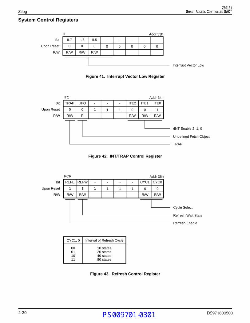
System Control Registers
IL7 IL6 - - -
0 0 0
R/W
0 0 0 0 0
R/W
Interrupt Vector Low
Addr 33h
Bit
Upon Reset
--IL5
IL
R/WR/W
Figure 41. Interrupt Vector Low Register
TRAP UFO ITE2 ITE1 ITE0
0 0 1 1 1 0
R/W
0 1
R/W
/INT Enable 2, 1, 0
Addr 34h
Bit
Upon Reset
---
ITC
R/WRR/W R/W
Undefined Fetch Object
TRAP
Figure 42. INT/TRAP Control Register
REFE REFW - CYC1 CYC0
1 1 1 1 1 1 0 0
R/W
Cycle Select
Addr 36h
Bit
Upon Reset
--
Refresh Wait State
Refresh Enable
-
RCR
R/WR/WR/W R/W
CYC1, 0
00011011
Interval of Refresh Cycle
10 states20 states40 states80 states
Figure 43. Refresh Control Register

2-31
Zilog
DS971800500
Z80181SMART ACCESS CONTROLLER SAC™
M1E /M1TE - - -
1 1 1 1 1 1 1 1
R/W
I/O Compatibility
Addr 3Eh
Bit
Upon Reset
--
/M1 Temporary Enable
/M1 Enable
/IOC
OMCR
WR/W R/W
Note: This register has to be programmed as 0x0xxxxxb(x:don't care) as a part of Initialization.
Figure 44. Operation Mode Control Register
IOA7 IOA6 - - -
0 0 0 1 1 1 1 1
R/W
I/O Stop
Addr 3Fh
Bit
Upon Reset
--
I/O AddressCombination of 11is reserved
IOSTP
ICR
R/WR/W R/W
Figure 45. I/O Control Register

2-32
Z80181SMART ACCESS CONTROLLER SAC™Zilog
DS971800500
CTC Control Registers
Channel Control WordThis word sets the operating modes and parameters asdescribed below. Bit D0 must be a “1” to indicate that thisis a Control Word (Figure 46).
For more detailed information, refer to the CTC TechnicalManual.
This register has the following fields:
Bit D7. Interrupt Enable. This bit enables the interrupt logicso that an internal INT is generated at zero count. Interruptsare programmed in either mode and may be enabled ordisabled at any time.
Bit D6. Mode Bit. This bit selects either Timer Mode orCounter Mode.
Bit D5. Prescaler Factor. This bit selects the prescalerfactor for use in the timer mode. Either divide-by-16 ordivide-by-256 is available.
Bit D4. Clock/Trigger Edge Selector. This bit selects theactive edge of the CLK/TRG input pulses.
Bit D3. Timer Trigger. This bit selects the trigger mode fortimer operation. Either automatic or external trigger may beselected.
Bit D2. Time Constant. This bit indicates that the next wordprogrammed is time constant data for the downcounter.
Bit D1. Software Reset. Writing a “1” to this bit indicates asoftware reset operation, which stops counting activitiesuntil another time constant word is written.
D7 D6 D5 D4 D3 D2 D1 D0
Control or Vector 0 Vector 1 Control Word
Reset 0 Continued Operation 1 Software Reset
Time Constant 0 No Time Constant Follows 1 Time Constant Follows
Time Trigger * 0 Automatic Trigger When Time Constant is Loaded 1 CLK/TRG Pulse Starts Timer
* Timer Mode Only
Interrupt 1 Enables Interrupt 0 Disables Interrupt
Mode 0 Selects Timer Mode 1 Selects Counter Mode
Prescaler Value * 1 Value of 256 0 Value of 16
CLK/TRG Edge Selection 0 Selects Falling Edge 1 Selects Rising Edge
Addr: E4h (Ch 0)E5h (Ch 1)E6h (Ch 2)E7h (Ch 3)
Figure 46. CTC Channel Control Word

2-33
Zilog
DS971800500
Z80181SMART ACCESS CONTROLLER SAC™
Time Constant WordBefore a channel can start counting, it must receive a timeconstant word. The time constant value may be anywherebetween 1 and 256, with “0” being accepted as a count of256 (Figure 47).
Interrupt Vector WordIf one or more of the CTC channels have interrupt enabled,then the Interrupt Vector Word is programmed. Only thefive most significant bits of this word are programmed, andbit D0 must be “0”. Bits D2-D1 are automatically modifiedby the CTC channels after responding with an interruptvector (Figure 48).
D7 D6 D5 D4 D3 D2 D1 D0
TC0
TC1
TC2
TC3
TC4
TC5
TC6
TC7
Figure 47. CTC Time Constant Word
D7 D6 D5 D4 D3 D2 D1 D0
0 Interrupt Vector Word1 Control Word
Channel Identifier(Automatically Insertedby CTC) 0 0 Channel 0 0 1 Channel 1 1 0 Channel 2 1 1 Channel 3
Supplied By User
Addr: E4h
Figure 48. CTC Interrupt Vector Word
SCC REGISTERS
For more detailed information, please refer to the Z8030/Z8530 SCC Technical Manual.
Note:The Address for the Control/Status Register is E8h. TheAddress for the Data Register is E9h.
Read RegistersThe SCC contains eight read registers. To read the con-tents of a register (rather than RR0), the program must firstinitialize a pointer to WR0 in exactly the same manner as awrite operation. The next I/O read cycle will place thecontents of the selected read registers onto the data bus(Figure 49).
Bit Description
RR0 Transmit and Receive buffer statusand external status.
RR1 Special Receive Condition status.RR2 Interrupt vector (modified if VIS Bit in WR9 is set).RR3 Interrupt pending bits.RR6 SDLC FIFO byte counter lower byte
(only when enabled).
Bit Description
RR7 SDLC FIFO byte count and status(only when enabled).
RR8 Receive buffer.RR10 Miscellaneous status bits.RR12 Lower byte of baud rate.RR13 Upper byte of baud rate generator time constant.RR15 External Status interrupt information.
Table 2. SCC Read Registers

2-34
Z80181SMART ACCESS CONTROLLER SAC™Zilog
DS971800500
SCC REGISTERS (Continued)
D7 D6 D5 D4 D3 D2 D1 D0
Rx Character Available
Read Register 0
Zero Count
Tx Buffer Empty
DCD
Sync/Hunt
CTS
Tx Underrun/EOM
Break/Abort
D7 D6 D5 D4 D3 D2 D1 D0
V0
Read Register 2
V1
V2
V3
V4
V5
V6
V7
Interrupt
Vector *
* Modified if VIS bit in Write register 9 is set.
D7 D6 D5 D4 D3 D2 D1 D0
All Sent
Read Register 1
Residue Code 2
Residue Code 1
Residue Code 0
Parity Error
Rx Overrun Error
CRC/Framing Error
End of Frame (SDLC)
D7 D6 D5 D4 D3 D2 D1 D0
0
Read Register 3
0
0
Ext/Status IP
Tx IP
Rx IP
0
0
(a)
(c)
(b) (d)
Figure 49. SCC Read Register Bit Functions

2-35
Zilog
DS971800500
Z80181SMART ACCESS CONTROLLER SAC™
D7 D6 D5 D4 D3 D2 D1 D0
BC0
Read Register 6 *
BC1
BC2
BC3
BC4
BC5
BC6
BC7
* Can only be accessed if the SDLC FIFO enhancement is enabled (WR15 bit D2 set to 1)
D7 D6 D5 D4 D3 D2 D1 D0
0
Read Register 10
On Loop
0
0
Loop Sending
0
Two Clocks Missing
One Clock Missing
(e) SDLC FIFO Status and Byte Count (LSB)
D7 D6 D5 D4 D3 D2 D1 D0
BC8
Read Register 7 *
BC9
BC10
BC11
BC12
BC13
FDA: FIFO Available Status1 Status Reads from FIFO
FOS: FIFO Overflow Status1 FIFO Overflowed0 Normal
* Can only be accessed if the SDLC FIFO enhancement is enabled (WR15 bit D2 set to 1)
D7 D6 D5 D4 D3 D2 D1 D0
TC0
Read Register 12
TC1
TC2
TC3
TC4
TC5
TC6
TC7
Lower Byteof Time Constant
(h)
(g)
Figure 49. SCC Read Register Bit Functions (Continued)
(f) SDLC FIFO Status and Byte Count (MSB)

2-36
Z80181SMART ACCESS CONTROLLER SAC™Zilog
DS971800500
SCC REGISTERS (Continued)
D7 D6 D5 D4 D3 D2 D1 D0
TC8
Read Register 13
TC9
TC10
TC11
TC12
TC13
TC14
TC15
Upper Byteof Time Constant
D7 D6 D5 D4 D3 D2 D1 D0
0
Read Register 15
Zero Count IE
0
DCD IE
Sync/Hunt IE
CTS IE
Tx Underrun/EOM IE
Break/Abort IE
(i) (j)
Figure 49. SCC Read Register Bit Functions (Continued)
Write RegistersThe SCC contains fifteen write registers that are pro-grammed to configure the operating modes of the chan-nel. With the exception of WR0, programming the writeregisters is a two step operation. The first operation is a
pointer written to WR0 that points to the selected register.The second operation is the actual control word that iswritten into the register to configure the SCC channel(Figure 50).
Bit Description
WR0 Register Pointers, various initializationcommands
WR1 Transmit and Receive interrupt enables,WAIT/DMA commands
WR2 Interrupt VectorWR3 Receive parameters and control modesWR4 Transmit and Receive modes and parametersWR5 Transmit parameters and control modesWR6 Sync Character or SDLC addressWR7 Sync Character or SDLC flag
Bit Description
WR8 Transmit bufferWR9 Master Interrupt control and reset commandsWR10 Miscellaneous transmit and receive control bitsWR11 Clock mode controls for receive and transmitWR12 Lower byte of baud rate generatorWR13 Upper byte of baud rate generatorWR14 Miscellaneous control bitsWR15 External status interrupt enable control
Table 3. SCC Write Registers

2-37
Zilog
DS971800500
Z80181SMART ACCESS CONTROLLER SAC™
D7 D6 D5 D4 D3 D2 D1 D0
0 0 0 Register 00 0 1 Register 10 1 0 Register 20 1 1 Register 31 0 0 Register 41 0 1 Register 51 1 0 Register 61 1 1 Register 70 0 0 Register 80 0 1 Register 90 1 0 Register 100 1 1 Register 111 0 0 Register 121 0 1 Register 131 1 0 Register 141 1 1 Register 15
With Point High Command
*
*
Write Register 0 (non-multiplexed bus mode)
0 0 0 Null Code0 0 1 Point High0 1 0 Reset Ext/Status Interrupts0 1 1 Send Abort (SDLC)1 0 0 Enable Int on Next Rx Character1 0 1 Reset Tx Int Pending1 1 0 Error Reset1 1 1 Reset Highest IUS
0 0 Null Code0 1 Reset Rx CRC Checker1 0 Reset Tx CRC Generator1 1 Reset Tx Underrun/EOM Latch
D7 D6 D5 D4 D3 D2 D1 D0
Write Register 1
Ext Int Enable
Tx Int Enable
Parity is SpecialCondition
0 0 Rx Int Disable0 1 Rx Int On First Character or Special Condition1 0 Int On All Rx Characters or Special Condition1 1 Rx Int On Special Condition Only
WAIT/DMA RequestOn Receive//Transmit
/WAIT/DMA RequestFunction
WAIT/DMA RequestEnable
(b)
(a)
D7 D6 D5 D4 D3 D2 D1 D0
V0
Write Register 2
V1
V2
V3
V4
V5
V6
V7
InterruptVector
(c)
Figure 50. Write Register Bit Functions

2-38
Z80181SMART ACCESS CONTROLLER SAC™Zilog
DS971800500
SCC REGISTERS (Continued)
D7 D6 D5 D4 D3 D2 D1 D0
Write Register 3
Rx Enable
0 0 Rx 5 Bits/Character0 1 Rx 7 Bits/Character1 0 Rx 6 Bits/Character1 1 Rx 8 Bits/Character
Sync Character Load Inhibit
Address Search Mode (SDLC)
Rx CRC Enable
Enter Hunt Mode
Auto Enables
(d)
D7 D6 D5 D4 D3 D2 D1 D0
Write Register 4
Parity Enable
0 0 X1 Clock Mode0 1 X16 Clock Mode1 0 X32 Clock Mode1 1 X64 Clock Mode
Parity EVEN//ODD
0 0 Sync Modes Enable0 1 1 Stop Bit/Character1 0 1 1/2 Stop Bits/Character1 1 2 Stop Bits/Character
0 0 8-Bit Sync Character0 1 16-Bit Sync Character1 0 SDLC Mode (01111110 Flag)1 1 External Sync Mode
D7 D6 D5 D4 D3 D2 D1 D0
Write Register 5
Tx CRC Enable
0 0 Tx 5 Bits(Or Less)/Character0 1 Tx 7 Bits/Character1 0 Tx 6 Bits/Character1 1 Tx 8 Bits/Character
RTS
/SDLC/CRC-16
Tx Enable
Send Break
DTR
(e)
(f)
Figure 50. Write Register Bit Functions (Continued)

2-39
Zilog
DS971800500
Z80181SMART ACCESS CONTROLLER SAC™
D7 D6 D5 D4 D3 D2 D1 D0
Write Register 6
Sync3Sync3Sync3 1ADR3 x
Sync2Sync2Sync2 1ADR2 x
Sync1Sync1Sync1 1ADR1 x
Sync0Sync0Sync0 1ADR0 x
Monosync, 8 BitsMonosync, 6 BitsBisync, 16 BitsBisync, 12 BitsSDLCSDLC (Address Range)
Sync4Sync4Sync4Sync0ADR4ADR4
Sync5Sync5Sync5Sync1ADR5ADR5
Sync6Sync0Sync6Sync2ADR6ADR6
Sync7Sync1Sync7Sync3ADR7ADR7
(g)
D7 D6 D5 D4 D3 D2 D1 D0
Write Register 7
Sync3Sync1Sync11Sync7 1
Sync2Sync0Sync10Sync6 1
Sync1 xSync9Sync5 1
Sync0 xSync8Sync4 0
Monosync, 8 BitsMonosync, 6 BitsBisync, 16 BitsBisync, 12 BitsSDLC
Sync4Sync2Sync12Sync8 1
Sync5Sync3Sync13Sync9 1
Sync6Sync4Sync14Sync10 1
Sync7Sync5Sync15Sync11 0
(h)
Figure 50. Write Register Bit Functions (Continued)

2-40
Z80181SMART ACCESS CONTROLLER SAC™Zilog
DS971800500
SCC REGISTERS (Continued)
D7 D6 D5 D4 D3 D2 D1 D0
Write Register 9
VIS
0 0 No Reset0 1 Reserved1 0 Channel Reset A1 1 Force Hardware Reset
NV
DLC
MIE
Status High//Status Low
0
D7 D6 D5 D4 D3 D2 D1 D0
Write Register 11
0 0 /TRxC Out - Xtal Output0 1 /TRxC Out - Transmit Clock1 0 /TRxC Out - BR Generator Output1 1 /TRxC Out - DPLL Output
/TRxC O/I
0 0 Transmit Clock - /RTxC Pin0 1 Transmit Clock - /TRxC Pin1 0 Transmit Clock - BR Generator Output1 1 Transmit Clock - DPLL Output
0 0 Receive Clock - /RTxC Pin0 1 Receive Clock - /TRxC Pin1 0 Receive Clock - BR Generator Output1 1 Receive Clock - DPLL Output
/RTxC Xtal//No Xtal
(k)
D7 D6 D5 D4 D3 D2 D1 D0
Write Register 10
6 Bit//8 Bit Sync
0 0 NRZ0 1 NRZI1 0 FM1 (Transition = 1)1 1 FM0 (Transition = 0)
Loop Mode
Abort//Flag On Underrun
Mark//Flag Idle
Go Active On Poll
CRC Preset I//O
D7 D6 D5 D4 D3 D2 D1 D0
TC0
Write Register 12
TC1
TC2
TC3
TC4
TC5
TC6
TC7
Lower Byte of Time Constant
(l)(j)
(i)
Figure 50. Write Register Bit Functions (Continued)

2-41
Zilog
DS971800500
Z80181SMART ACCESS CONTROLLER SAC™
D7 D6 D5 D4 D3 D2 D1 D0
TC8
Write Register 13
TC9
TC10
TC11
TC12
TC13
TC14
TC15
Upper Byte of Time Constant
D7 D6 D5 D4 D3 D2 D1 D0
Write Register 14
0 0 0 Null Command0 0 1 Enter Search Mode0 1 0 Reset Missing Clock0 1 1 Disable DPLL1 0 0 Set Source = BR Generator1 0 1 Set Source = /RTxC1 1 0 Set FM Mode1 1 1 Set NRZI Mode
BR Generator Enable
BR Generator Source
/DTR/Request Function
Auto Echo
Local Loopback
(n)
(m)
D7 D6 D5 D4 D3 D2 D1 D0
0
Write Register 15
Zero Count IE
SDLC FIFO Enable
DCD IE
Sync/Hunt IE
CTS IE
Tx Underrun/EOM IE
Break/Abort IE
(o)
Figure 50. Write Register Bit Functions (Continued)

2-42
Z80181SMART ACCESS CONTROLLER SAC™Zilog
DS971800500
PIA Control Registers
PIA1 Data Direction Register (P1DDR, I/O Address E0h),PIA1 Data Port (P1DP, I/O address E1h), PIA2 Data Direc-tion Register (P2DDR, I/O Address E2h) and PIA2 DataRegister (P2DP, I/O Address E3h). These four registers are
shown in Figures 51-54. Note that if the CTC/PIA bit in theSystem Configuration Register is set to one, the CTC I/Ofunctions override the PIA1 function, and programming ofP1DDR is ignored.
Figure 51. PIA 1 Data Direction Register
7 6 5 4 3 2 1 0
1 - Input0 - Output
E2H
1 - Input0 - Output
1 - Input0 - Output
1 - Input0 - Output
1 - Input0 - Output
1 - Input0 - Output
1 - Input0 - Output
1 - Input0 - Output
7 6 5 4 3 2 1 0
1 - Input0 - Output
E0H
1 - Input0 - Output
1 - Input0 - Output
1 - Input0 - Output
1 - Input0 - Output
1 - Input0 - Output
1 - Input0 - Output
1 - Input0 - Output
Figure 53. PIA 2 Data Direction Register
7 6 5 4 3 2 1 0
PIA 1I/O Data
E1H
7 6 5 4 3 2 1 0
PIA 2I/O Data
E3H
Figure 54. PIA 2 Data RegisterFigure 52. PIA 1 Data Register
The Data Port is the register to/from the 8-bit parallel port.At power on Reset, they are initialized to 1.
The Data Direction Register has eight control bits. Individ-ual bits specify each bit's direction. When the bit is set to
a "1", the bit becomes an input, otherwise it is an output. Onreset, these registers are initialized to 1, resulting in all linesbeing inputs.

2-43
Zilog
DS971800500
Z80181SMART ACCESS CONTROLLER SAC™
REGISTERS FOR SYSTEM CONFIGURATION
There are four registers to determine system configurationwith the Z181. These registers are: RAM upper boundaryaddress register (RAMUBR, I/O address EAh), RAM lowerboundary address register (RAMLBR, I/O address EBh),ROM address boundary register (ROMBR, I/O addressECh) and System Configuration Register (SCR, I/O ad-dress EDh).
ROM Address Boundary Register(ROMBR, I/O Address ECh)This register specifies the address range for the /ROMCSsignal. When accessed memory addresses are less thanor equal to the value programmed in this register, the/ROMCS signal is asserted (Figure 55).
The A18 signal from the CPU is obtained before it ismultiplexed with “TOUT”. This signal can be forced to “1”(inactive state) by setting Bit D5 of the System Configura-tion Register, to allow the user to overlay the RAM area overthe ROM area. At power-up reset, this register contains all1's so that /ROMCS is asserted for all addresses.
RAM Lower Boundary Address Register (RAMLBR, I/O Address EBh) and RAM Upper BoundaryAddress Register (RAMUBR, I/O Address EAh)These two registers specify the address range for the/RAMCS signal. When accessed memory addresses areless than or equal to the value programmed in the RAMUBRand greater than or equal to the value programmed in the
RAMLBR, /RAMCS is asserted. (Figure 13) The A18 signalfrom the CPU is taken before it is multiplexed with “T
OUT”.
In the case that these register are programmed to overlap,/ROMCS takes priority over /RAMCS (/ROMCS is assertedand /RAMCS is inactive).
Chip Select signals are going active for the address range:
/ROMCS: (ROMBR) ≥ A19-A12 ≥ 0/RAMCS: (RAMUBR) ≥ A19-A12 > (RAMLBR)
These registers are set to “FFh” at power-on Reset, and theboundary addresses of ROM and RAM are the following:
ROM lower boundary address(fixed) = 00000h
ROM upper boundary address(ROMBR register) = 0FFFFFh
RAM lower boundary address(RAMLBR register) = 0FFFFFh
RAM upper boundary address(RAMUBR register) = 0FFFFFh
Since /ROMCS takes priority over /RAMCS, the latter willnever be asserted until the value in the ROMBR andRAMLBR registers are re-initialized to lower values.
7 6 5 4 3 2 1 0
A12
EAH
A13
A14
A15
A16
A17
A18
A19
Figure 55. RAM Upper Boundary Register
7 6 5 4 3 2 1 0
A12
EBH
A13
A14
A15
A16
A17
A18
A19
Figure 56. RAM Lower Boundary Register

2-44
Z80181SMART ACCESS CONTROLLER SAC™Zilog
DS971800500
REGISTERS FOR SYSTEM CONFIGURATION (Continued)
7 6 5 4 3 2 1 0
A12
ECH
A13
A14
A15
A16
A17
A18
A19
Figure 57. ROM Boundary Register
Figure 58. System Configuration Register
7 6 5 4 3 2 1 0
PIA1/CTIO 1 PIA1 Functions as CTC's I/O Pins 0 PIA1 Functions as I/O Port
EDH
Reserved - Program as 0
ROM Emulator Mode (REME) 1 Data Bus in ROM Emulator Mode 0 Data Bus in Normal Mode
Reserved - Program as 0
Reserved - Program as 0
Disable /ROMCS 1 /ROMCS is Disabled 0 /ROMCS is Enabled
Daisy Chain Configuration 1 IEI Pin-CTC-SCC-IEO Pin 0 IEI Pin-SCC-CTC-IEO Pin
Reserved - Program as 0

2-45
Zilog
DS971800500
Z80181SMART ACCESS CONTROLLER SAC™
System Configuration Register (I/O address EDh)This register is to determine the functionality of PIA1 andthe Interrupt Daisy-Chain Configuration (Figure 13). Thisregister has the following control bits:
Bit D7. Reserved and should be programmed as “0”.
Bit D6. Daisy-Chain Configuration. Determines thearrangement of the interrupt priority daisy chain.
When this bit is set to “1”, priority is as follows:
IEI pin - CTC - SCC - IEO pin
When this bit is “0”, priority is as follows:
IEI pin - SCC - CTC - IEO pin
This bit’s default (after Reset) is 0.
Bit D5. Disable /ROMCS. When this bit is set to “1”./ROMCS is forced to a “1” regardless of the status of theaddress decode logic. This bit’s default (after Reset) is 0and /ROMCS function is enabled.
Bit D4-D3. Reserved and should be programmed as “00”.
Bit D2. ROM Emulator Mode Enable. When this bit is set toa 1, the Z181 is in “ROM emulator mode”. In this mode, busdirection for certain transaction periods are set to theopposite direction to export internal bus transactions out-side the Z80181. This allows the use of ROM emulators/logic analyzers for applications development. This bit’sdefault (after Reset) is 0.
Bit D1. Reserved and shall be programmed as “0”.
Bit D0. CTC/PIA1. When this bit is set to “1”, PIA1 functionsas the CTC’s I/O pins. This bit’s default (after Reset) is 0.

2-46
Z80181SMART ACCESS CONTROLLER SAC™Zilog
DS971800500
Data Bus Direction
Table 4 shows the state of the SAC’s data bus when in SACbus master condition.
Table 4. Data Bus Direction (Z181 Is Bus Master)
I/O And Memory Transactions
I/O I/O I/O I/O Write Read Refresh Z80181Write To Read From Write To Read From To From IdleOn-Chip On-Chip Off-Chip Off-Chip Memory Memory ModePeripherals Peripherals Peripheral Peripheral(SCC/CTC/ (SCC/CTC/PIA1/PIA2) PIA1/PIA2)
Z80181 Data Bus Out Z Out In Out In Z Z(REME Bit = 0)
Z80181 Data Bus Out Out Out In Out In Z Z(REME Bit = 1)
Interrupt Acknowledge Transaction
Intack For Intack ForOn-Chip Off-Chip
Peripheral Peripheral
(SCC/CTC)
Z80181 Data Bus Z In(REME Bit = 0)
Z80181 Data Bus Out In(REME Bit = 1)

2-47
Zilog
DS971800500
Z80181SMART ACCESS CONTROLLER SAC™
Table 5 shows the state of the SAC’s data bus when theZ80181 is NOT in bus master condition.
Table 5. Data Bus Direction for External Bus Master (Z80181 Is Not Bus Master)
I/O And Memory Transactions
I/O I/O I/O I/O Write Read Refresh Z80181Write To Read From Write To Read From To From IdleOn-Chip On-Chip Off-Chip Off-Chip Memory Memory ModePeripherals Peripherals Peripheral Peripheral(SCC/CTC/ (SCC/CTC/PIA1/PIA2) PIA1/PIA2)
Z80181 Data Bus In Out Z Z Z In Z Z(REME Bit = 0)
Z80181 Data Bus In Out Z Z Z In Z Z(REME Bit = 1)
Interrupt Acknowledge Transaction
Intack For Intack ForOn-Chip Off-ChipPeripheral Peripheral(SCC/CTC)
Z80181 Data Bus Out In(REME Bit = 0)
Z80181 Data Bus Out In(REME Bit = 1)
The word “OUT” means that the Z181 data bus direction isin output mode, “IN” means input mode, and “HI-Z” meanshigh impedance.
“REME” stands for “ROM Emulator Mode” and is the statusof D2 bit in the System Configuration Register.

2-48
Z80181SMART ACCESS CONTROLLER SAC™Zilog
DS971800500
ABSOLUTE MAXIMUM RATINGS
Voltage on VCC
with respect to VSS
........... –0.3V to +7.0VVoltages on all inputs
with respect to VSS
........................... –0.3V to VCC
+0.3VStorage Temperature ............................–65°C to +150°COperating Ambient
Temperature ........................ See Ordering Information
Stresses greater than those listed under Absolute Maxi-mum Ratings may cause permanent damage to the de-vice. This is a stress rating only; operation of the device atany condition above those indicated in the operationalsections of these specifications is not implied. Exposure toabsolute maximum rating conditions for extended periodsmay affect device reliability.
STANDARD TEST CONDITIONS
The DC Characteristics and capacitance sections belowapply for the following standard test conditions, unlessotherwise noted. All voltages are referenced to GND (0V).Positive current flows into the referenced pin (Figure 59).
Available operatingtemperature range is: E = –40°C to +100°C
Voltage Supply Range: +4.50V ≤ Vcc ≤ + 5.50V
All AC parameters assume a load capacitance of 100 pF.Add 10 ns delay for each 50 pF increase in load up to amaximum of 150 pF for the data bus and 100 pF foraddress and control lines. AC timing measurements arereferenced to 1.5 volts (except for clock, which is refer-enced to the 10% and 90% points). Maximum capacitiveload for CLK is 125 pF.
+5V
From Output Under Test
100 pf 250 µA
2.1 K
Figure 59. Standard Test Circuit

2-49
Zilog
DS971800500
Z80181SMART ACCESS CONTROLLER SAC™
DC CHARACTERISTICSZ80181
Symbol Parameter Min Typ Max Unit Condition
VIH1 Input “H” Voltage VCC –0.6 VCC +0.3 V/RESET, EXTAL, /NMI
VIH2 Input “H” Voltage 2.0 VCC +0.3 VExcept /RESET, EXTAL, /NMI
VIL1
Input “L” Voltage –0.3 0.6 V/RESET, EXTAL, /NMI
VIL2
Input “L” Voltage –0.3 0.8 VExcept /RESET, EXTAL, /NMI
VOH
Output “H” Voltage 2.4 V IOH
= -200 µAAll outputs. V
CC –1.2 I
OH = – 20 µA
VOL
Output “L” Voltage 0.45 V IOL
= 2.2 mAAll outputs.
IIL
Input Leakage 10 µA VIN = 0.5 – V
CC –0.5
Current All InputsExcept XTAL, EXTAL
ITL
Tri-State Leakage Current 10 µA VIN = 0.5 – V
CC –0.5
ICC* Power Dissipation*(Normal Operation) 25 80 f = 10 MHzPower Dissipation*(SYSTEM STOP mode) 6.3 40 f = 10 MHz
Cp Pin Capacitance 12 pF VIN = 0V, f = 1 MHz
TA = 25°C
Notes:* V
IH Min = V
CC -1.0V, V
IL Max = 0.8V (all output terminals are at no load.)
VCC
= 5.0V

2-50
Z80181SMART ACCESS CONTROLLER SAC™Zilog
DS971800500
AC CHARACTERISTICSZ180 MPU Timing
Figures 60-68 show the timing for the Z181 MPU and the referenced parameters appear in Table A.
Ø
T1 T2 Tw T3 T1
4 5
1
6
3
2
20 19 20
19
11
8 12
13
9 14
10
17
18
15 16
6261
67 66 67 66
6261
Address
/WAIT
/MREQ
/RD
/M1
ST
/IORQ/WR
Data In
/RESET
"H"
7
/ROMCS/RAMCS
70 70
Figure 60a. Opcode Fetch Cycle

2-51
Zilog
DS971800500
Z80181SMART ACCESS CONTROLLER SAC™
Ø
T1 T2 Twa T3 T1
6
70 70
2019
11287
27
9 12 11
22 24
25, 25a
15 16
23
21
26
Address
/ROMCS/RAMCS
/WAIT
/IORQ
/RD
/WR
Data IN
Data OUT
ST"H"
[1]
[1] Output buffer is off at this point.[2] Memory Read/Write cycle timing is the same as this figure, except there is no automatic wait status (Twa), and /MREQ is active instead of /IORQ.
Figure 60b. I/O Read/Write, Memory Read/Write Timing

2-52
Z80181SMART ACCESS CONTROLLER SAC™Zilog
DS971800500
AC CHARACTERISTICS (Continued)Z180 MPU Timing
Ø
31
30
32
29
15
16
38
3940 42
33
34 34
33
3635
3737
42[3]
/INTI
/NMI
/M1 [1]
/IORQ [1]
/Data IN [1]
/MREQ [2]
/RFSH [2]
/BUSREQ
/BUSACK
AddressData /MREQ,
/RD, /WR,/IORQ
/HALT
43
C7
/INTSCC [4]
Notes:[1] During /INT0 acknowledge cycle[2] During refresh cycle
[3] Output buffer is off at this point[4] Refer to Table C, parameter 7
Figure 61. CPU Timing(/INT0 Acknowledge Cycle, Refresh Cycle, BUS RELEASE Mode
HALT Mode, SLEEP Mode, SYSTEM STOP Mode)

2-53
Zilog
DS971800500
Z80181SMART ACCESS CONTROLLER SAC™
Ø
T1 T2 Tw T3 T1 T2 Tw T3
27
Address
/IORQ
/RD
/WR
I/O Read Cycle I/O Write Cycle
9
28 27 28
2422
13
Figure 62. CPU Timing (/IOC = 0)(I/O Read Cycle, I/O Write Cycle)

2-54
Z80181SMART ACCESS CONTROLLER SAC™Zilog
DS971800500
AC CHARACTERISTICS (Continued)Z180 MPU Timing
Ø
44
45
44
45
46
17
47
18
CPU or DMA Read/Write Cycle (Only DMA Write Cycle for /TENDi)
T1 T2 Tw T3 T1
[3]
[4]
[2]
[1]
/DREQi(At level
sense)
/DREQi(At edge
sence)
/TENDi
ST
DMA Control Signals[1] tDRQS and tDRQH are specified for the rising edge of clock followed by T3.[2] tDRQS and tDRQH are specified for the rising edge of clock.[3] DMA cycle starts.[4] CPU cycle starts.
Figure 63. DMA Control Signals

2-55
Zilog
DS971800500
Z80181SMART ACCESS CONTROLLER SAC™
Ø
T1 T2 Tw Tw T3
E(Memory
Read/Write)
E(I/O Read)
D7-D0
48 49
48 49
48 49
16
E(I/O Read)
4848
Ø
E
15
BUS RELEASE ModeSLEEP ModeSYSTEM STOP Mode
(a) E Clock Timing(Memory Read/Write Cycle, I/O Read/Write Cycle)
(b) E Clock Timing(BUS RELEASE Mode, SLEEP Mode, SYSTEM STOP Mode)
Figure 64. E Clock Timing

2-56
Z80181SMART ACCESS CONTROLLER SAC™Zilog
DS971800500
AC CHARACTERISTICS (Continued)Z180 MPU Timing
Ø
T2 Tw T3 T1 T2
E(Example: I/O Read -
Op-code Fetch)
53
48
51
49
52
50
52
48
49
53
E(I/O Write)
Figure 65. E Clock Timing(Minimum timing example of PWEL and PWEH)
Ø
54
A18/TOUT
Timer DataReg = 0000H
Figure 66. Timer Output Timing

2-57
Zilog
DS971800500
Z80181SMART ACCESS CONTROLLER SAC™
Ø
T3 T1 T2 TS TS T1 T2
31
30
32
42 43
/INTi
/NMI
A18-A0
/MREQ, /M1/RD
/HALT
SLP Instruction Fetch Next Op-code Fetch
Figure 67. SLP Execution Cycle

2-58
Z80181SMART ACCESS CONTROLLER SAC™Zilog
DS971800500
AC CHARACTERISTICS (Continued)Z180 MPU Timing
CSI/O Clock
5656
5857 5857
6059 59 60
11.5 tcyc
11 tcyc 11 tcyc
11.5 tcyc
16.5 tcyc 16.5 tcyc
55 55
Transmit Data(Internal Clock)
Transmit Data(External Clock)
Receive Data(Internal Clock)
Receive Data(External Clock)
Figure 68. CSI/O Receive/Transmit Timing
Table A. Z180 CPU & 180 Peripherals Timing
Z8018110No Symbol Parameter Min Max Unit
1 tcyc Clock Cycle Time 100 2000 ns2 tCHW Clock Pulse Width (High) 40 ns3 tCLW Clock Pulse Width (Low) 40 ns4 tcf Clock Fall Time 10 ns
5 tcr Clock Rise Time 10 ns6 tAD Address Valid from Clock Rise 70 ns7 tAS Address Valid to /MREQ, /IORQ Fall 10 ns8 tMED1 Clock Fall to /MREQ Fall Delay 50 ns9 tRDD1 Clock Fall to /RD Fall (/IOC=1) 50 ns
Clock Rise to /RD Fall (/IOC=0) 55 ns10 tM1D1 Clock Rise to /M1 Fall Delay 60 ns

2-59
Zilog
DS971800500
Z80181SMART ACCESS CONTROLLER SAC™
Table A. Z180 CPU & 180 Peripherals Timing (Continued)
Z8018110No Symbol Parameter Min Max Unit
11 tAH Address Hold Time 10 ns(/MREQ, /IORQ, /RD, /WR)
12 tMED2 Clock Fall to /MREQ Rise Delay 50 ns13 tRDD2 Clock Fall to /RD Rise Delay 50 ns14 tM1D2 Clock Rise to /M1 Rise Delay 60 ns15 tDRS Data Read Setup Time 25 ns
16 tDRH Data Read Hold Time 0 ns17 tSTD1 Clock Fall to ST Fall 60 ns18 tSTD2 Clock Fall to ST Rise 60 ns19 tWS /WAIT Setup Time to Clock Fall 30 ns20 tWH /WAIT Hold time from Clock Fall 30 ns
21 tWDZ Clock Rise to Data Float Delay 60 ns22 tWRD1 Clock Rise to /WR Fall Delay 50 ns23 tWDO /WR fall to Data Out Delay 10 ns24 tWRD2 Clock Fall to /WR Rise 50 ns25 tWRP /WR Pulse Width 110 ns
(Memory Write Cycles)
25a /WR Pulse Width (I/O Write Cycles) 210 ns26 tWDH Write Data Hold Time from /WR Rise 10 ns27 tIOD1 Clock Fall to /IORQ Fall Delay 50 ns
(/IOC=1)Clock Rise to /IORQ Fall Delay 55 ns(/IOC=0)
28 tIOD2 Clock Fall /IOQR Rise Delay 50 ns
29 tIOD3 /M1 Fall to /IORQ Fall Delay 200 ns30 tINTS /INT Setup Time to Clock Fall 30 ns31 tINTH /INT Hold Time from Clock Fall 30 ns32 tNMIW /NMI Pulse Width 80 ns33 tBRS /BUSREQ Setup Time to Clock Fall 30 ns
34 tBRH /BUSREQ Hold Time from Clock Fall 30 ns35 tBAD1 Clock Rise to /BUSACK Fall Delay 60 ns36 tBAD2 Clock Fall to /BUSACK Rise Delay 60 ns37 tBZD Clock Rise to Bus Floating Delay Time 80 ns
38 tMEWH /MREQ Pulse Width (High) 70 ns39 tMEWL /MREQ Pulse Width (Low) 80 ns40 tRFD1 Clock Rise to /RFSH Fall Delay 60 ns41 tRFD2 Clock Rise to /RFSH Rise Delay 60 ns42 tHAD1 Clock Rise to /HALT Fall Delay 50 ns
43 tHAD2 Clock Rise to /HALT Rise Delay 50 ns44 tDRQS /DREQi Setup Time to Clock Rise 30 ns45 tDRQH /DREQi Hold Time from Clock Rise 30 ns46 tTED1 Clock Fall to /TENDi Fall Delay 50 ns

2-60
Z80181SMART ACCESS CONTROLLER SAC™Zilog
DS971800500
AC CHARACTERISTICS (Continued)Z180™ MPU Timing
Table A. Z180 CPU &180 Peripherals Timing (Continued)
Z8018110No Symbol Parameter Min Max Unit
47 tTED2 Clock Fall to /TENDi Rise Delay 50 ns48 tED1 Clock Rise to E Rise Delay 60 ns49 tED2 Clock Edge to E Fall Delay 60 ns50 PWEH E Pulse Width (High) 55 ns51 PWEL E Pulse Width (Low) 110 ns
52 tEr Enable Rise Time 20 ns53 tEf Enable Fall Time 20 ns54 tTOD Clock Fall to Timer Output Delay 150 ns55 tSTDI CSI/O Tx Data Delay Time 150 ns
(Internal Clock Operation)56 tSTDE CSI/O Tx Data Delay Time 7.5tcyc+150 ns
(External Clock Operation)
57 tSRSI CSI/O Rx Data Setup Time 1 tcyc(Internal Clock Operation)
58 tSRHI CSI/O Rx Data Hold Time 1 tcyc(Internal Clock Operation)
59 tSRSE CSI/O Rx Data Setup Time 1 tcyc(External Clock Operation)
60 tSRHE CSI/O Rx Data Hold Time 1 tcyc(External Clock Operation)
61 tRES /RESET Setup Time to Clock Fall 80 ns62 tREH /RESET Hold Time from Clock Fall 50 ns63 tOSC Oscillator Stabilization Time 20 ms64 tEXr External Clock Rise Time (EXTAL) 25 ns65 tEXf External Clock Fall Time (EXTAL) 25 ns
66 tRr /RESET Rise Time 50 ns67 tRf /RESET Fall Time 50 ns68 tIr Input Rise Time 100 ns
(Except EXTAL, /RESET)69 tIf Input Fall Time 100 ns
(Except EXTAL, /RESET)70 TdCS(A) Address Valid to /ROMCS, /RAMCS 20 ns
Valid Delay

2-61
Zilog
DS971800500
Z80181SMART ACCESS CONTROLLER SAC™
AC CHARACTERISTICS (Continued)CTC Timing
Figure 69 shows the timing for the on-chip CTC. Param-eters referenced in this figure appear in Table B.
Clock
CLK/TRGCounter
5
6 7
2
3 10
1
11
4
9 8
CLK/TRGTimer
ZC/TO
/INT
Figure 69. CTC Timing
Table B. CTC Timing Parameters
Z8018110No Symbol Parameter Min Max Unit Note
1 TdCr(INTf) Clock Rise to /INT Fall Delay (TcC+100) ns [B1]2 TsCTRr(Cr)c CLK/TRG Rise to Clock Rise
Setup Time for Immediate Count 90 ns [B2]3 TsCTR(Ct) CLK/TRG Rise to Clock Rise
Setup Time for Enabling of Prescaler 90 ns [B1]On Following Clock Rise
4 TdCTRr(INTf) CLK/TRG Rise to /INT Fall DelayTsCTR(C) Satisfied (1)+(3) ns [B2]TsCTR(C) Not Satisfied TcC+(1)+(3) ns [B2]
5 TcCTR CLK/TRG Cycle Time (2TcC) DC ns [B3]6 TwCTRh CLK/TRG Width (Low) 90 DC ns7 TwCTRl CLK/TRG Width (High) 90 DC ns8 TrCTR CLK/TRG Rise Time 30 ns
9 TfCTR CLK/TRG Fall Time 30 ns10 TdCr(ZCr) Clock Rise to ZC/TO Rise Delay 80 ns11 TdCf(ZCf) Clock Fall to ZC/TO Fall Delay 80 ns
Notes for Table B:[B1] Timer Mode[B2] Counter Mode[B3] Counter Mode Only. When using a cycle time less than 3TcC, parameter #2 must be met.

2-62
Z80181SMART ACCESS CONTROLLER SAC™Zilog
DS971800500
AC CHARACTERISTICS (Continued)SCC Timing
Figure 70 shows the AC characteristics for the on-chipSCC. Parameters referenced in this figure appear inTable C.
Ø
2
3
4
6
5
1
/WR
/RD
/W//REQWait
/W//REQRequest
/DTR//REQRequest
/INT
Figure 70. SCC AC Parameters
Table C. SCC Timing Parameters (85C30 AC Characteristics)
Z8018110No Symbol Parameter Min Max Unit Note
1 TdWR(W) /WR Fall to Wait Valid Delay 180 + TcC ns [C1]2 TdWR(W) /RD Fall to Wait Valid Delay 180 ns [C1]3 TdWRf(REQ) /WR Fall to /W//REQ Not Valid Delay 180 + TcC ns4 TdRDf(REQ) /RD Fall to /W//REQ Not Valid Delay 180 ns
5 TdWRr(REQ) /WR Rise to /DTR//REQ Not Valid Delay 5TcC ns6 TdPC(INT) Clock to /INT Valid Delay 500 ns [C1]7 TdRDA(INT) /M1 Fall to /INT Inactive Delay TBS ns [C1]
Note for Table C:[C1] Open-drain output, measured with open-drain test load.

2-63
Zilog
DS971800500
Z80181SMART ACCESS CONTROLLER SAC™
Figure 71 shows the general timing for the on-chip SCC.Parameters referenced in this figure appear in Table D.
PCLK
1
2
/W//REQRequest
/W//REQWait
/RTxC, /TRxCReceive
RxD
/SYNCExternal
/TRxC, /RTxCTransmit
TxD
/TRxCOutput
/RTxC
/TRxC
/CTS, /DCD
/SYNCInput
4 6
7 8
9 10
11
12
13
14
15, 21
16
17
19
19
20
20
53
18, 21
Figure 71. SCC General Timing

2-64
Z80181SMART ACCESS CONTROLLER SAC™Zilog
DS971800500
AC CHARACTERISTICS (Continued)SCC General Timing
Table D. SCC General Timing Parameters
Z8018110No Symbol Parameter Min Max Unit Note
1 TdPC(REQ) Clock Fall to /W//REQ Valid 200 ns2 TdPC(W) Clock Fall to Wait Inactive 300 ns3 TsRXD(RXCr) RxD to /RxC Rise Setup Time 0 ns [D1]4 ThRXD(RXCr) RxD to /RxC Rise Hold Time 125 ns [D1]
5 TsRXD(RXCf) RxD to /RxC Fall Setup Time 0 ns [D1,4]6 ThRXD(RXCf) RxD to /RxC Fall Hold Time 125 ns [D1,4]7 TsSY(RXC) /SYNC to /RxC Setup Time –150 ns [D1]8 ThSY(RXC) /SYNC to /RxC Hold Time 5TcC ns [D1]
9 TdTXCf(TXD) /TxC Fall to TxD Delay 150 ns [D2]10 TdTXCr(TXD) /TxC Rise to TxD Delay 150 ns [D2,4]11 TdTXD(TRX) TxD to /TRxC Delay 140 ns12 TwRTXh /RTxC High Width 120 ns [D5]13 TwRTXl /RTxC Low Width 120 ns [D5]
14 TcRTX /RTxC Cycle Time (RxD, TxD) 400 ns [D5,6]15 TcRTXX Xtal OSC Period 100 1000 ns [D3]16 TwTRXh /TRxC High Width 120 ns [D5]17 TwTRXl /TRxC Low Width 120 ns [D5]
18 TcTRX /TRxC Cycle Time 400 ns [D5,7]19 TwEXT /DCD or /CTS Pulse Width 120 ns20 TwSY /SYNC Pulse Width 100 ns21 TxRx(DPLL) DPLL Cycle Time 50 ns [D6,7]
Notes to Table D:[D1] /RXC is /RTxC or /TRxC, whichever is supplying the receiver clock.[D2] /TXC is /TRxC or /RTxC, whichever is supplying the transmitter clock.[D3] Both /RTxC and /SYNC pins have 30 pF Capacitors (to Ground).[D4] Parameter applies only to FM encoding/decoding.[D5] Parameter applies only to transmitter and receiver; baud rate generator timing requirements are different.[D6] The maximum receive or transmit data rate is 1/4 TcC.[D7] Applies to DPLL clock source only; maximum data rate of 1/4 TcC still applies.

2-65
Zilog
DS971800500
Z80181SMART ACCESS CONTROLLER SAC™
Figure 72 shows the system timing for the on-chip SCC.Parameters referenced in this figure appear in Table E.
/RTxC, /TRxCReceive
/W//REQRequest
/W//REQWait
/SYNCOutput
/INT
/RTxC, /TRxCTransmit
/W//REQRequest
10
9
8
7
6
1
2
3
4
5
/W//REQWait
/INT
/DTR//REQRequest
/CTS, /DCD
/SYNCInput
/INT
Figure 72. SCC System Timing

2-66
Z80181SMART ACCESS CONTROLLER SAC™Zilog
DS971800500
AC CHARACTERISTICS (Continued)SCC System Timing
Table E. SCC System Timing Parameters
Z8018110No Symbol Parameter Min Max Unit Note
1 TdRxC(REQ) /RxC to /W//REQ Valid 8 12 TcC [E2]2 TdRxC(W) /RxC to Wait inactive 8 14 TcC [E1,2]3 TdRxC(SY) /RxC to /SYNC Valid 4 7 TcC [E2]4 TdRxC(INT) /RxC to /INT Valid 10 16 TcC [E1,2]5 TdTxC(REQ) /TxC to /W//REQ Valid 5 8 TcC [E3]
6 TdTxC(W) /TxC to Wait inactive 5 11 TcC [E1,3]7 TdRxC(DRQ) /TxC to /DTR//REQ Valid 4 7 TcC [E3]8 TdTxC(INT) /TxC to /INT Valid 6 10 TcC [E1,3]9 TdSY(INT) /SYNC to /INT Valid 2 6 TcC [E1]10 TdEXT(INT) /DCD or /CTS to /INT Valid 2 6 TcC [E1]
Notes for Table E:[E1] Open-drain output, measured with open-drain test load.[E2] /RXC is /RTxC or /TRxC, whichever is supplying the receiver clock.[E3] /TXC is /TRxC or /RTxC, whichever is supplying the transmitter clock.

2-67
Zilog
DS971800500
Z80181SMART ACCESS CONTROLLER SAC™
AC CHARACTERISTICS (Continued)PIA General-Purpose I/O Port Timing
Figure 73 shows the timing for the PIA ports. Parametersreferenced in this figure appear in Table F.
Ø
T1 T2 Tw T3
1
2
/IORQ, /RD
PIA Input
PIA Output
Figure 73. PIA Timing
Table F. PIA General-Purpose I/O Timing Parameters
Z8018110No Symbol Parameter Min Max Unit
1 TsPIA(C) PIA Data Setup time to Clock Rise 10 ns2 TdCr(PIA) Clock Rise to PIA Data Valid Delay 50 ns

2-68
Z80181SMART ACCESS CONTROLLER SAC™Zilog
DS971800500
AC CHARACTERISTICS (Continued)Interrupt Daisy-Chain Timing
Figure 74 shows the interrupt daisy-chain timing. Parame-ters referenced in this figure appear in Table G.
1 3
2 45
6
CLK
/M1
/IORQ
Data
IEI
9
7, 8
10
11
IEO
/INT(SCC)
/WAIT
Figure 74. Interrupt Daisy-Chain Timing
Table G. Interrupt Daisy-Chain Timing Parameters
Z8018110No Symbol Parameter Min Max Unit
1 TsM1(Cr) /M1 Fall to Clock Rise Setup Time 20 ns
2 TsM1(IO)INTA /M1 Fall to /IORQ Fall Setup Time(During INTACK Cycle) 2TcC ns
3 Th Hold Time 04 TdM1r(DOz) /M1 Rise to Data Out Float Delay 0 ns5 TdCr(DO) Clock Rise to Data Out Delay
6 TsIEI(TW4) IEI to TW4
Rise Setup Time 95 ns7 TdIEIf(IEOf) IEI Fall to IEO Fall Delay8 TdIEIr(IEOr) IEO Rise to IEO Rise Delay9 TdM1f(IEOf) /M1 Fall to IEO Fall Delay10 TdCWA(f)INTA Clock Rise to /WAIT Fall Delay11 TdCWA(r)INTA Clock Rise to /WAIT Rise Delay

2-69
Zilog
DS971800500
Z80181SMART ACCESS CONTROLLER SAC™
Note for Interrupt Acknowledge Cycle andDaisy Chain
When using the interrupt daisy chained device(s) for otherthan the Z181 (without external logic), the following restric-tions/notes apply:
The device(s) must be connected to the higher prioritylocation (Figure 75).
The device(s) IEI-IEO delay must be less than two clockcycles.
The Z181 on-chip interface logic inserts another three waitstates into the interrupt acknowledge cycle to meet the on-chip SCC and the Z80 CTC timing requirements. (For atotal of five wait states, including the two automaticallyinserted wait states).
To meet the timing requirements, the Z181’s on-chip circuitgenerates interface signals for the SCC and CTC.Figure 78 has the timing during the interrupt acknowledgecycle, including the internally generated signals.
The following are three separate cases for the daisy-chainsettle times:
Case 1 - SCC: The SCC /INTACK signal goes active on theT1 clock fall time. The settle time is from SCC /INTACKactive until the SCC /RD signal goes active on the fourthrising wait state clock.
Case 2 - CTC: The settle time for the on-chip /IORQ isbetween the fall of /M1 until the internal CTC /IORQ goesactive on the rise of the fourth wait state (the same time asSCC /RD goes active).
Case 3 - OFF-chip Z80 Peripheral: The settle time for theoff-chip Z80 peripheral is from the fall of /M1 until CTC/IORQ goes active. Since the Z181’s external /IORQ signalgoes active on the clock fall of the first automaticallyinserted wait state (T
WA), the external daisy-chain device
must be connected to the upper chain location. Also, itmust settle within two clock cycles.
If any peripheral is connected externally with a lower daisychain priority than Z181 peripherals, /IORQ must be de-layed by external logic as shown in Figure 79.
Vcc
IEI IEO IEI IEOIEI IEO CTC SCCPeripheralDevice(s)
Z80181
Figure 75. Peripheral Device as Part of the Daisy Chain

2-70
Z80181SMART ACCESS CONTROLLER SAC™Zilog
DS971800500
AC CHARACTERISTICS (Continued)Read Write External BUS Master Timing
CLK
Address
1
2 3
3
6511
10
4
7
12
3
98
Data IN
Data OUT
A7-A0
/IORQ
/RD
Data
/WR
Data
Figure 76. Read/Write External BUS Master Timing
Table H. External Bus Master Interface Timing (Read/Write Cycles)
Z8018110No Symbol Parameter Min Max Unit
1 TsA(Cr) Address to CLK Rise Setup Time 20 ns2 TsIO(Cr) /IORQ Fall to CLK Rise Setup Time 20 ns3 Th Hold Time 04 TsRD(Cr) /RD Fall to CLK Rise Setup Time 20 ns5 TdRD(DO) /RD Fall to Data Out Delay 120 ns
6 TdRIr(DOz) /RD, /IORQ Rise to Read Data Float 07 TsWR(Cr) /WR Fall to CLK Rise Setup Time 20 ns8 TsDi(WRf) Data in to /WR Fall Setup Time 09 ThWIr(Di) /IORQ, /WR Rise to Data In Hold Time 0
10 TsA(IORQf) Address to /IORQ Fall Setup Time 50 ns11 TsA(RDf) Address to /RD Fall Setup Time 50 ns12 TsA(WRf) Address to /WR Fall Setup Time 50 ns

2-71
Zilog
DS971800500
Z80181SMART ACCESS CONTROLLER SAC™
SCC External BUS Master Timing
1
2
Valid SCC Addr * IORQ
/RD or /WR
DTR/REQRequest
Figure 77. SCC External BUS Master Timing
Table I. External Bus Master Interface Timing (SCC Related Timing)
Z8018110No Symbol Parameter Min Max Unit Notes
1 TrC Valid Access Recovery Time 4TcC ns [1]2 TdRDr(REQ) /RD Rise to /DTR//REQ Not Valid Delay 4TcC ns
Note for Table I:[1] Only applies between transactions involving the SCC.

2-72
Z80181SMART ACCESS CONTROLLER SAC™Zilog
DS971800500
AC CHARACTERISTICS (Continued)
CLK
/M1
T T T1 2 WA WA W W W 3T T T T T
Settle Time for Off-chip Z80 Peripherals
Settle Time forOn-chip CTC
Settle Timefor SCC
/IORQ
SCC/INTACK
/WAIT
SCC/RD
CTC/IORQ
/WAIT Signal generated by interface circuit
Figure 78. Interrupt Acknowledge Cycle Timing
Vcc
IEI IEO IEI IEO IEI IEOCTC SCCPeripheralDevice(s)
ExternalLogic to Extend/IORQSignalZ80181
/IORQ
Figure 79. Peripheral Device as Part of the Daisy Chain

2-73
Zilog
DS971800500
Z80181SMART ACCESS CONTROLLER SAC™
PACKAGE INFORMATION
100-Pin QFP Package Diagram

2-74
Z80181SMART ACCESS CONTROLLER SAC™Zilog
DS971800500
ORDERING INFORMATION
Z80181 (10 MHz)Extended Temperature
100-Pin QFPZ8018110FEC
PackageLonger Lead TimeF = Plastic Quad Flat Pack
TemperatureLonger Lead TimeE = –40°C to +100°C
EnvironmentalC = Plastic Standard
Speed10 = 10 MHz
Example:Z 80181 10 F E C is a Z80181, 10 MHz, QFP, –40°C to +100°C, Plastic Standard Flow
Environmental FlowTemperaturePackageSpeedProduct NumberZilog Prefix
Zilog’s products are not authorized for use as critical compo-nents in life support devices or systems unless a specific writtenagreement pertaining to such intended use is executed betweenthe customer and Zilog prior to use. Life support devices orsystems are those which are intended for surgical implantationinto the body, or which sustains life whose failure to perform,when properly used in accordance with instructions for useprovided in the labeling, can be reasonably expected to result insignificant injury to the user.
Zilog, Inc. 210 East Hacienda Ave.Campbell, CA 95008-6600Telephone (408) 370-8000Telex 910-338-7621FAX 408 370-8056Internet: http://www.zilog.com
© 1997 by Zilog, Inc. All rights reserved. No part of this documentmay be copied or reproduced in any form or by any meanswithout the prior written consent of Zilog, Inc. The information inthis document is subject to change without notice. Devices soldby Zilog, Inc. are covered by warranty and patent indemnificationprovisions appearing in Zilog, Inc. Terms and Conditions of Saleonly. Zilog, Inc. makes no warranty, express, statutory, implied orby description, regarding the information set forth herein orregarding the freedom of the described devices from intellectualproperty infringement. Zilog, Inc. makes no warranty of mer-chantability or fitness for any purpose. Zilog, Inc. shall not beresponsible for any errors that may appear in this document.Zilog, Inc. makes no commitment to update or keep current theinformation contained in this document.