Embed Size (px)
Citation preview
PIONEER CORPORATION 4-1, Meguro 1-chome,PIONEER ELECTRONICS (USA) INC. P.O. Box 1760, LonPIONEER EUROPE NV Haven 1087, Keetberglaan 1, 912PIONEER ELECTRONICS ASIACENTRE PTE. LTD. 253
PIONEER CORPORATION 2004
PHONES
6 DVD/CD0 OPEN/CLOSE FM/AM VOL.– DOWN UP +7 STANDBY/ON
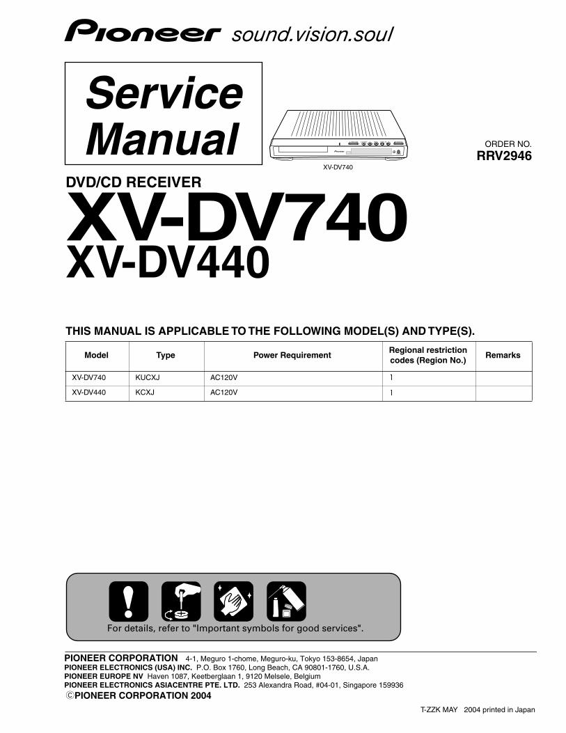
XV-DV740
Meguro-ku, Tokyo 153-8654, Japang Beach, CA 90801-1760, U.S.A.
0 Melsele, BelgiumAlexandra Road, #04-01, Singapore 159936
ORDER NO.
RRV2946
DVD/CD RECEIVER
XV-DV740XV-DV440THIS MANUAL IS APPLICABLE TO THE FOLLOWING MODEL(S) AND TYPE(S).
Model Type Power RequirementRegional restriction codes (Region No.)
Remarks
XV-DV740 KUCXJ AC120V
XV-DV440 KCXJ AC120V
For details, refer to "Important symbols for good services".
T-ZZK MAY 2004 printed in Japan
C
D
F
A
B
E
1 2 3 4
SAFETY INFORMATION
This service manual is intended for qualified service technicians; it is not meant for the casualdo-it-yourselfer. Qualified technicians have the necessary test equipment and tools, and have beentrained to properly and safely repair complex products such as those covered by this manual.Improperly performed repairs can adversely affect the safety and reliability of the product and mayvoid the warranty. If you are not qualified to perform the repair of this product properly and safely, youshould not risk trying to do so and refer the repair to a qualified service technician.
WARNING
This product contains lead in solder and certain electrical parts contain chemicals which are known to the state of California to
cause cancer, bir th defects or other reproductive harm.
Health & Safety Code Section 25249.6 – Proposition 65
NOTICE
(FOR CANADIAN MODEL ONLY)
Fuse symbols (fast operating fuse) and/or (slow operating fuse) on PCB indicate that replacement
parts must be of identical designation.
REMARQUE
(POUR MODÈLE CANADIEN SEULEMENT)
Les symboles de fusible (fusible de type rapide) et/ou (fusible de type lent) sur CCI indiquent que
les pièces de remplacement doivent avoir la même désignation.
ANY MEASUREMENTS NOT WITHIN THELIMITS OUTLINED ABOVE ARE INDICATIVEOF A POTENTIAL SHOCK HAZARD ANDMUST BE CORRECTED BEFORE RETURN-ING THE APPLIANCE TO THE CUSTOMER.
2. PRODUCT SAFETY NOTICEMany electrical and mechanical parts in the appliance
have special safety related character istics. These areoften not evident f rom visual inspect ion nor theprotection afforded by them necessarily can be obtainedby using replacement components rated for voltage,wattage, etc. Replacement par ts which have thesespecial safety character ist ics are identif ied in thisService Manual.
Electr ical components having such features areidentified by marking with a on the schematics andon the parts list in this Service Manual.The use of a substitute replacement component whichdoes not have the same safety characteristics as thePIONEER recommended replacement one, shown in theparts list in this Service Manual, may create shock, fire,or other hazards.
Product Safety is continuously under review and newinstructions are issued from time to time. For the latestinformation, always consult the current PIONEERService Manual. A subscription to, or additional copiesof, PIONEER Service Manual may be obtained at anominal charge from PIONEER.
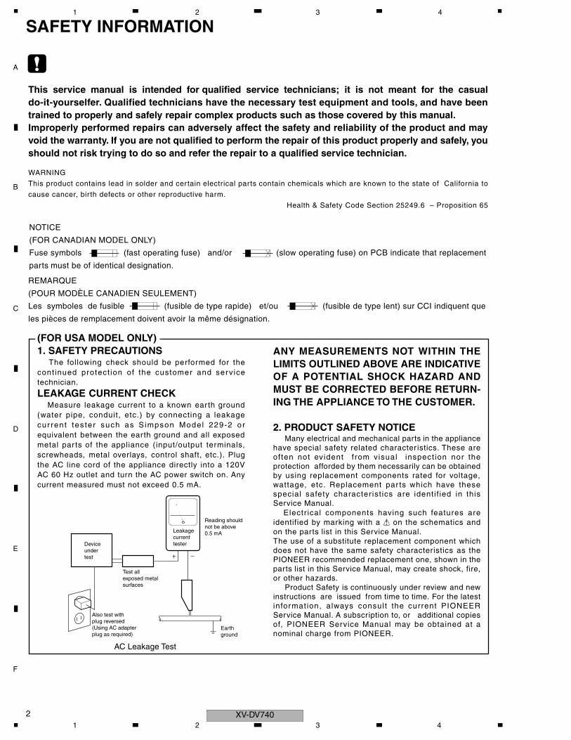
(FOR USA MODEL ONLY)1. SAFETY PRECAUTIONS
The following check should be performed for thecont inued protect ion of the customer and servicetechnician.
LEAKAGE CURRENT CHECKMeasure leakage current to a known ear th ground
(water pipe, conduit, etc.) by connecting a leakagecurrent tes ter such as S impson Model 229-2 orequivalent between the earth ground and all exposedmetal par ts of the appliance (input/output terminals,screwheads, metal overlays, control shaft, etc.). Plugthe AC line cord of the appliance directly into a 120VAC 60 Hz outlet and turn the AC power switch on. Anycurrent measured must not exceed 0.5 mA.
Deviceundertest
Leakagecurrenttester
Earthground
Reading shouldnot be above0.5 mA
Also test withplug reversed(Using AC adapterplug as required)
Test allexposed metalsurfaces
AC Leakage Test
XV-DV74021 2 3 4
C
D
F
A
B
E
3
5 6 7 8
[ Important symbols for good services ]In this manual, the symbols shown-below indicate that adjustments, settings or cleaning should be made securely.When you find the procedures bearing any of the symbols, be sure to fulfill them:
2. Adjustments
To keep the original performances of the product, optimum adjustments or specification confirmation is indispensable. In accordance with the procedures or instructions described in this manual, adjustments should be performed.
3. Cleaning
For optical pickups, tape-deck heads, lenses and mirrors used in projection monitors, and other parts requiring cleaning,proper cleaning should be performed to restore their performances.
5. Lubricants, glues, and replacement partsAppropriately applying grease or glue can maintain the product performances. But improper lubrication or applying glue may lead to failures or troubles in the product. By following the instructions in this manual, be sure to apply theprescribed grease or glue to proper portions by the appropriate amount.For replacement parts or tools, the prescribed ones should be used.
4. Shipping mode and shipping screws
To protect the product from damages or failures that may be caused during transit, the shipping mode should be set orthe shipping screws should be installed before shipping out in accordance with this manual, if necessary.
1. Product safety
You should conform to the regulations governing the product (safety, radio and noise, and other regulations), and should keep the safety during servicing by following the safety instructions described in this manual.
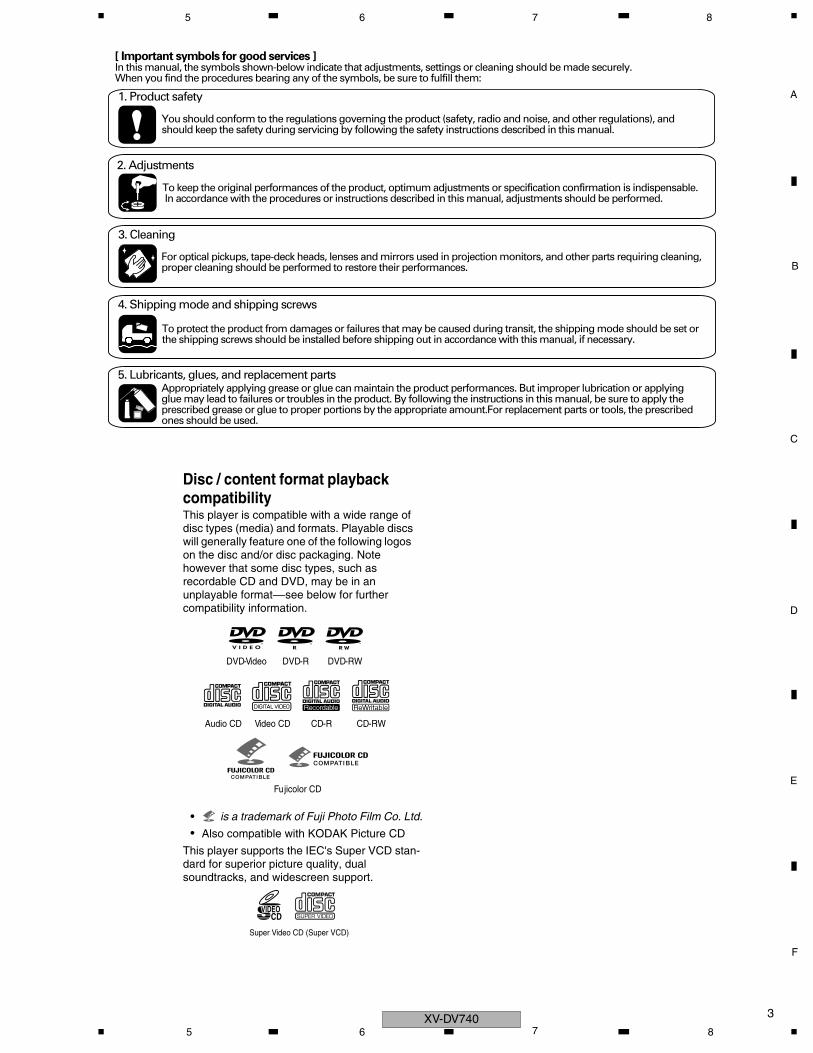
Disc / content format playback compatibilityThis player is compatible with a wide range of disc types (media) and formats. Playable discs will generally feature one of the following logos on the disc and/or disc packaging. Note however that some disc types, such as recordable CD and DVD, may be in an unplayable format––see below for further compatibility information.
• •
is a trademark of Fuji Photo Film Co. Ltd.
Also compatible with KODAK Picture CD
This player supports the IEC's Super VCD stan-dard for superior picture quality, dual soundtracks, and widescreen support.
DVD-Video DVD-R DVD-RW
Video CD
Fujicolor CD
Audio CD CD-R CD-RW
VIDEOCD
Super Video CD (Super VCD)
XV-DV7405 6 7 8
C
D
F
A
B
E
XV-DV7404
1 2 3 4
CONTENTS
SAFETY INFORMATION..................................................................................................................................... 21. SPECIFICATIONS ............................................................................................................................................ 52. EXPLODED VIEWS AND PARTS LIST ............................................................................................................ 6
2.1 PACKING ................................................................................................................................................... 62.2 EXTERIOR SECTION................................................................................................................................ 82.3 FRONT PANEL SECTION ....................................................................................................................... 102.4 01 LOADER ASSY................................................................................................................................... 122.5 TRAVERSE MECHA ASSY-S .................................................................................................................. 14
3. BLOCK DIAGRAM AND SCHEMATIC DIAGRAM.......................................................................................... 163.1 BLOCK DIAGRAM ................................................................................................................................... 163.2 LOAB ASSY and OVERALL WIRING DIAGRAM..................................................................................... 183.3 DVDM ASSY(1/3)..................................................................................................................................... 203.4 DVDM ASSY(2/3)..................................................................................................................................... 223.5 DVDM ASSY(3/3)..................................................................................................................................... 243.6 DSP ASSY (1/2)....................................................................................................................................... 263.7 DSP ASSY (2/2)....................................................................................................................................... 283.8 6CH AMP ASSY ...................................................................................................................................... 303.9 CONTROL(1/4), TRADE3 and TRADE2 ASSYS ..................................................................................... 323.10 CONTROL ASSY(2/4)............................................................................................................................ 343.11 CONTROL ASSY(3/4)............................................................................................................................ 363.12 CONTROL ASSY(4/4) and HP ASSYS.................................................................................................. 383.13 POWER ASSY(1/2)................................................................................................................................ 403.14 POWER ASSY(2/2) and TRADE1 ASSYS............................................................................................. 423.15 VIDEO ASSY ......................................................................................................................................... 443.16 DISPALY ASSY ...................................................................................................................................... 463.17 WAVEFORMS ........................................................................................................................................ 48
4. PCB CONNECTION DIAGRAM ..................................................................................................................... 494.1 LOAB ASSY............................................................................................................................................. 494.2 DVDM ASSY ............................................................................................................................................ 504.3 DSP ASSY ............................................................................................................................................... 524.4 6CH AMP ASSY ...................................................................................................................................... 544.5 CONTROL ASSY..................................................................................................................................... 564.6 TRADE2,TRADE3 and HP ASSYS.......................................................................................................... 604.7 POWER ASSY ......................................................................................................................................... 624.8 TRADE1, VIDEO and DISPLAY ASSYS .................................................................................................. 66
5. PCB PARTS LIST ........................................................................................................................................... 706. ADJUSTMENT ............................................................................................................................................... 76
6.1 ADJUSTMENT ITEMS AND LOCATION ................................................................................................. 766.2 JIGS AND MEASURING INSTRUMENTS............................................................................................... 766.3 NECESSARY ADJUSTMENT POINTS ................................................................................................... 776.4 TEST MODE ............................................................................................................................................ 786.5 MECHANISM ADJUSTMENT.................................................................................................................. 79
7. GENERAL INFORMATION............................................................................................................................. 817.1 DIAGNOSIS ............................................................................................................................................. 817.1.1 TEST MODE ......................................................................................................................................... 817.1.2 DISPLAY SPECIFICATIONS OF THE TEST MODE............................................................................. 837.1.3 FUNCTIONAL SPECIFICATION OF THE SHORTCUT KEY................................................................ 847.1.4 SPECIFICATION OF MODEL INFORMATION DISPLAY...................................................................... 857.1.5 FUNCTIONAL SPECIFICATION OF THE SERVICE MODE................................................................. 867.1.6 MECHANICAL ERROR HISTORY........................................................................................................ 877.1.7 ID NUMBER AND DATA SETTING ....................................................................................................... 927.1.8 METHOD FOR DIAGNOSING DEGRADATION OF THE LDS ON THE PICKUP ASSY...................... 957.1.9 TROUBLE SHOOTING ......................................................................................................................... 967.1.10 DSP TROUBLE SHOOTING............................................................................................................... 997.1.11 DISASSEMBLY ................................................................................................................................. 1017.2 IC ........................................................................................................................................................... 1107.3 EXPLANATION ...................................................................................................................................... 1137.3.1 SEQUENCE AFTER POWER ON ...................................................................................................... 1137.3.2 PROTECTION CIRCUIT ..................................................................................................................... 1147.4 CLEANING............................................................................................................................................. 118
8. PANEL FACILITIES ...................................................................................................................................... 119
1 2 3 4
C
D
F
A
B
E
5
5 6 7 8
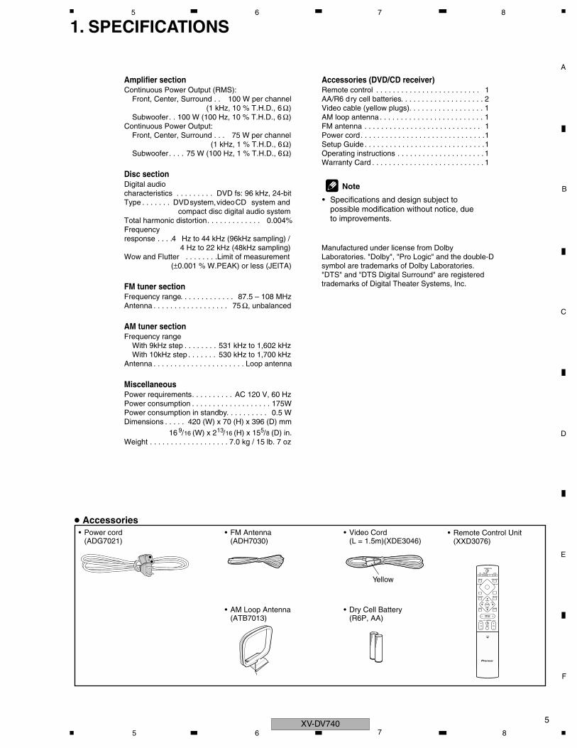
1. SPECIFICATIONS
Amplifier sectionContinuous Power Output (RMS):
Front, Center, Surround . . 100 W per channel(1 kHz, 10 % T.H.D., 6 Ω)
Subwoofer. . 100 W (100 Hz, 10 % T.H.D., 6 Ω)Continuous Power Output:
Front, Center, Surround . . . 75 W per channel(1 kHz, 1 % T.H.D., 6 Ω)
Subwoofer. . . . 75 W (100 Hz, 1 % T.H.D., 6 Ω)
Disc sectionDigital audio characteristics . . . . . . . . . DVD fs: 96 kHz, 24-bitType . . . . . . . DVD system, video CD system and
compact disc digital audio systemTotal harmonic distortion. . . . . . . . . . . . . 0.004%Frequency response . . . .4 Hz to 44 kHz (96kHz sampling) /
4 Hz to 22 kHz (48kHz sampling)Wow and Flutter . . . . . . . .Limit of measurement
(±0.001 % W.PEAK) or less (JEITA)
FM tuner sectionFrequency range. . . . . . . . . . . . . 87.5 – 108 MHzAntenna . . . . . . . . . . . . . . . . . . 75 Ω, unbalanced
AM tuner sectionFrequency range
With 9kHz step . . . . . . . . 531 kHz to 1,602 kHzWith 10kHz step . . . . . . . 530 kHz to 1,700 kHz
Antenna . . . . . . . . . . . . . . . . . . . . . . Loop antenna
MiscellaneousPower requirements. . . . . . . . . . AC 120 V, 60 HzPower consumption . . . . . . . . . . . . . . . . . . . 175WPower consumption in standby. . . . . . . . . . 0.5 WDimensions . . . . . 420 (W) x 70 (H) x 396 (D) mm
16 9/16 (W) x 2 13/16 (H) x 15 5/8 (D) in.Weight . . . . . . . . . . . . . . . . . . . 7.0 kg / 15 lb. 7 oz
Accessories (DVD/CD receiver)Remote control . . . . . . . . . . . . . . . . . . . . . . . . . 1AA/R6 dry cell batteries. . . . . . . . . . . . . . . . . . . . 2Video cable (yellow plugs). . . . . . . . . . . . . . . . . . 1AM loop antenna . . . . . . . . . . . . . . . . . . . . . . . . . 1FM antenna . . . . . . . . . . . . . . . . . . . . . . . . . . . . 1Power cord. . . . . . . . . . . . . . . . . . . . . . . . . . . . . .1Setup Guide . . . . . . . . . . . . . . . . . . . . . . . . . . . . .1Operating instructions . . . . . . . . . . . . . . . . . . . . . 1Warranty Card . . . . . . . . . . . . . . . . . . . . . . . . . . . 1
Note
• Specifications and design subject to possible modification without notice, due to improvements.
ST+
TUNE+
ENTER
TUNE–
MASTERVOLUME
ST–
STANDBY/ON
CD FM/AM
OPEN CLOSEDISPLAY
DVD TUNER TV LINE
L1/L2
DVD MENU RETURN
SOUND
TV CONTROL
CH VOLINPUT
OPEN
MUTE
Accessories• Power cord
(ADG7021)• FM Antenna
(ADH7030)
• AM Loop Antenna(ATB7013)
• Video Cord(L = 1.5m)(XDE3046)
• Remote Control Unit(XXD3076)
• Dry Cell Battery(R6P, AA)
Yellow
Manufactured under license from DolbyLaboratories. "Dolby", "Pro Logic" and the double-Dsymbol are trademarks of Dolby Laboratories."DTS" and "DTS Digital Surround" are registeredtrademarks of Digital Theater Systems, Inc.
XV-DV7405 6 7 8
C
D
F
A
B
E
XV-DV7406
1 2 3 4
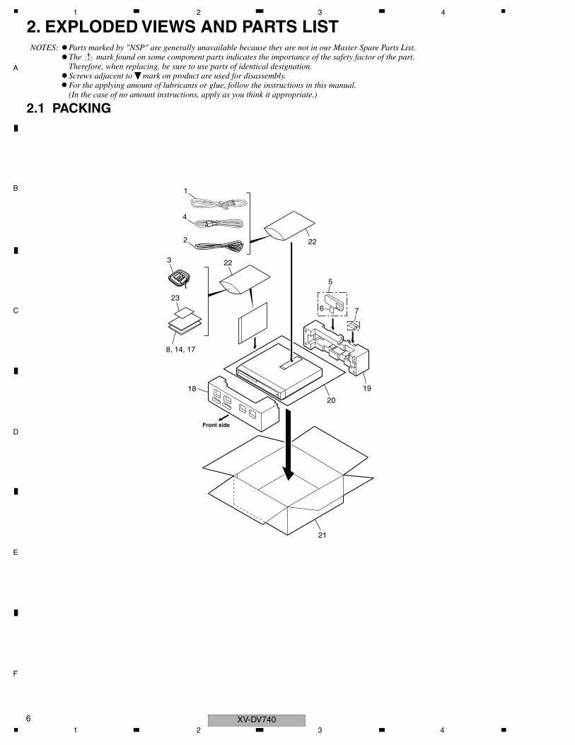
2. EXPLODED VIEWS AND PARTS LIST
2.1 PACKING
Parts marked by "NSP" are generally unavailable because they are not in our Master Spare Parts List.The mark found on some component parts indicates the importance of the safety factor of the part.Therefore, when replacing, be sure to use parts of identical designation.Screws adjacent to mark on product are used for disassembly. For the applying amount of lubricants or glue, follow the instructions in this manual.(In the case of no amount instructions, apply as you think it appropriate.)
NOTES:
Front side
5
7
19
20
18
6
22
22
3
23
8, 14, 17
1
4
2
21
1 2 3 4
C
D
F
A
B
E
7
5 6 7 8
PACKING SECTION Parts List
(2) CONTRAST TABLE
XV-DV740/KUCXJ and XV-DV440/KCXJ are constructed the same except for the following :
Mark No. Description Part No.
>
1 Power Cord ADG7021
2 FM Wire Antenna ADH7030
3 AM Loop Antenna ATB7013
4 Video Cord XDE3046
5 Remote Control XXD3076
6 Battery Cover XZN3130
NSP 7 Dry Cell Batteries (R6P/AA) VEM1031
8 Operating Instructions XRB3037
(English)
9 • • • • • •
10 • • • • • •
11 • • • • • •
12 • • • • • •
13 • • • • • •
14 Operating Instructions XRC3147
(French)
15 • • • • • •
16 • • • • • •
17 Operating Instructions See Contrast table (2)
(English/French)
18 Front Pad XHA3145
19 Rear Pad XHA3146
20 Packing Sheet AHG7010
21 Packing Case See Contrast table (2)
NSP 22 Polyethylene Bag Z21-038
NSP 23 Warranty Card ARY7045
Mark No. Description Part No.
Mark No. Description XV-DV740/KUCXJ XV-DV440/KCXJ
17 Operating Instructions (English/French)
XRE3084 XRE3081
21 Packing Case XHD3433 XHD3453
XV-DV7405 6 7 8
C
D
F
A
B
E
XV-DV7408
1 2 3 4
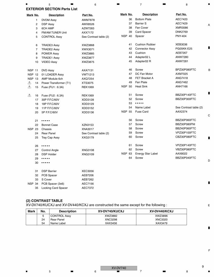
2.2 EXTERIOR SECTION
A
AB
B
I
C
G
FE
D
F
G
H
ED
C
L
K
H
LK
CO
NT
AC
T S
IDE
NO
N-C
ON
TA
CT
S
IDE
I
55
55
Refer to"2.3 FRONT PANEL SECTION".
43
43
57
57
5
6 2
1
3434
28
3111
62
37
27
32
32
36
62
62
62
62
50
3
9
19
7
4
8
51
51
51
48
58
5151
49
23
14 58
5149
52
48
48
47
51
51
17
18
15
16
54
33
33
27
42
46
46
46
46
44
45
3824
13
595959
595956
5656
56
56
56
59
56
56
56 56
35
39
39
39
56
56
56
22
64
57
57
F
K
H
D
J
C
B
G
25
51
61
60
60
63
56
5656
62
12
56
56
56
40
Refer to"2.4 01 LOADER ASSY".
41
20
10L
1 2 3 4
C
D
F
A
B
E
9
5 6 7 8
EXTERIOR SECTION Parts List
(2) CONTRAST TABLE
XV-DV740/KUCXJ and XV-DV440/KCXJ are constructed the same except for the following :
Mark No. Description Part No.
1 DVDM Assy AWM7878
2 DSP Assy AWX8526
3 6CH AMP AZW7283
4 FM/AM TUNER Unit AXX7172
5 CONTROL Assy See Contrast table (2)
6 TRADE3 Assy XWZ3868
7 TRADE2 Assy XWX3071
8 POWER Assy XWZ3885
9 TRADE1 Assy XWZ3877
10 VIDEO Assy XWZ3875
NSP 11 DVD Assy AXA7131
NSP 12 01 LOADER Assy VWT1213
NSP 13 AMP Module 6ch AXQ7254
>
14 Power Transformer (T1) XTS3075
>
15 Fuse (FU1 : 6.3A) REK1069
>
16 Fuse (FU2 : 6.3A) REK1069
17 30P F.F.C/60V XDD3128
18 18P F.F.C/60V XDD3129
19 11P F.F.C/60V XDD3152
20 5P F.F.C/60V XDD3136
21 • • • • •
22 Bonnet Case XZN3153
NSP 23 Chassis XNA3017
24 Rear Panel See Contrast table (2)
25 Tray Cap Assy XXG3179
26 • • • • •
27 Control Angle XNG3108
28 DSP Holder XNG3109
29 • • • • •
30 • • • • •
31 DSP Barrier XEC3056
32 PCB Spacer AEB7206
33 S Cover AEB7262
NSP 34 PCB Spacer (3x6) AEC7156
35 Locking Card Spacer AEC7372
36 Bottom Plate AEC7420
37 Barrier S AEC7429
38 Fan Cover XMR3086
39 Card Spacer DNK2769
NSP 40 Spacer PNY-404
41 Cushion Rubber XEB3036
42 Connector Assy PG05KK-E25
43 Cushion AEB7267
44 Adapter02 L ANW7280
45 Adapter02 R ANW7281
46 Screw BPZ30P080FTC
47 DC Fan Motor AXM7025
48 FET Bracket A ANG7418
49 Fan Plate ANG7462
NSP 50 Heat Sink ANH7166
51 Screw BBZ30P140FTC
52 Screw BBZ30P300FTC
53 • • • • •
54 Name Label See Contrast table (2)
NSP 55 Fuse Card AAX2374
56 Screw BBZ30P060FTC
57 Screw BBZ30P080FNI
58 Screw BBZ40P060FTC
59 Screw VPZ30P100FTC
60 Screw CBZ30P080FTC
61 Screw VPZ30P140FTC
62 Screw VBZ30P080FTC
NSP 63 Energy Star Label AAX8022
64 Screw BBZ30P040FTC
Mark No. Description Part No.
Mark No. Description XV-DV740/KUCXJ XV-DV440/KCXJ
5 CONTROL Assy XWZ3882 XWZ389624 Rear Panel XNC3298 XNC332054 Name Label XAX3456 XAX3479
XV-DV7405 6 7 8
C
D
F
A
B
E
XV-DV74010
1 2 3 4
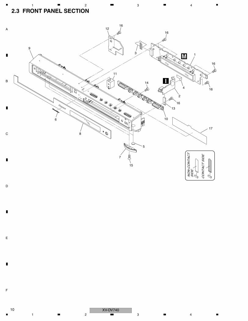
2.3 FRONT PANEL SECTION
CO
NT
AC
T S
IDE
NO
N-C
ON
TA
CT
S
IDE
M
I
8
9
6
1
4
2
13
14
11
10
5
7
1216
16
16
16
16
3
17
15
1 2 3 4
C
D
F
A
B
E
11
5 6 7 8
FRONT PANEL SECTION Parts List
(2) CONTRAST TABLEXV-DV740/KUCXJ and XV-DV440/KCXJ are constructed the same except for the following :
Mark No. Description Part No.
1 DISPLAY Assy XWZ3874
2 HP Assy XWZ3869
3 15P F.F.C/60V XDD3155
4 5P F.F.C/60V XDD3131
5 Leg AEB7090
6 Pioneer Name Plate VAM1136
7 Foot XMR3088
8 Display Window XAK3450
9 Front Panel See Contrast table (2)
10 FUNC. Button XAD3185
11 Top Lens XAK3453
12 Support PCB • • • • •
13 Support PCB • • • • •
14 Screw BPZ30P080FTC
15 Screw CBZ30P080FTC
16 Screw VPZ30P100FTC
17 F.L Barrier XEC3055
Mark No. Description Part No.
Mark No. Description XV-DV740/KUCXJ XV-DV440/KCXJ9 Front Panel XMB3155 XMB3170
XV-DV7405 6 7 8
C
D
F
A
B
E
XV-DV74012
1 2 3 4
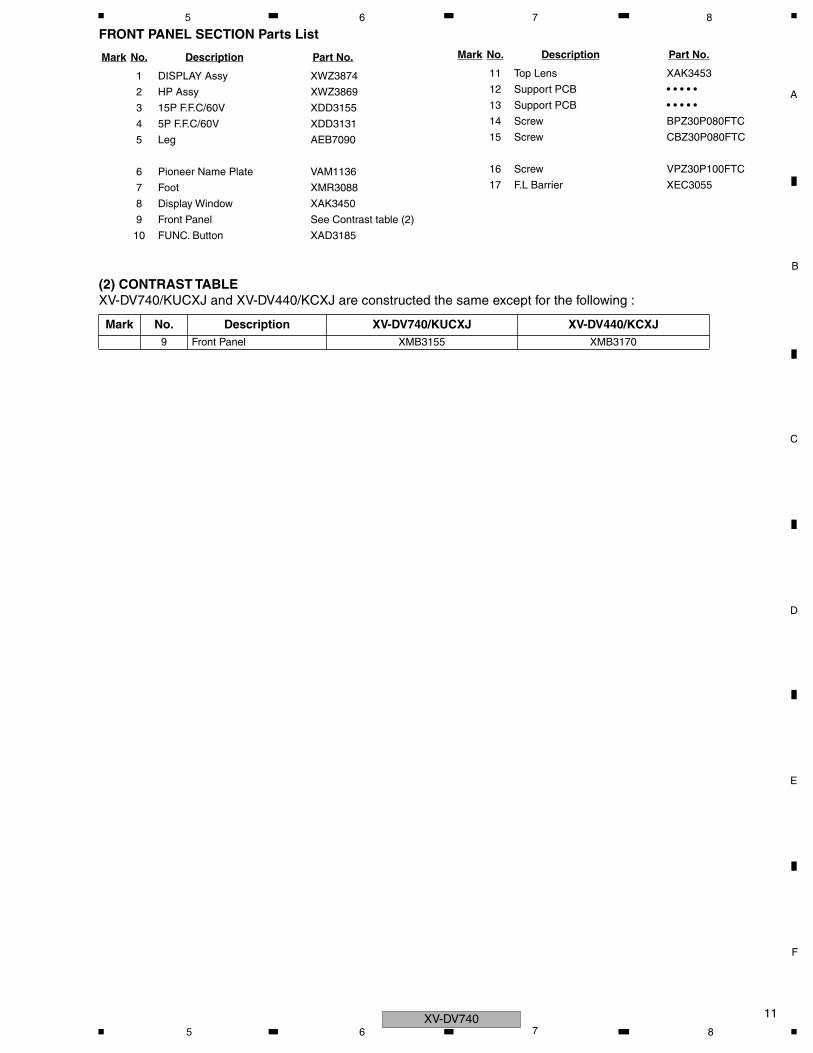
2.4 01 LOADER ASSY
01 LOADER ASSY Parts List
A
A
2
3
54
12
2313
17
21
16
22
15
14
22
22
22
2018
19
91
7
1011
6
8
8
8
8
A
Refer to"2.5 TRAVERSE MECHA. ASSY-S".
Lubricating OilGYA1001
DaifreeGEM1036
Refer to" Application of Lubricant".
Note :
Lubricating OilGYA1001
To DVDM CN101 (Pickup Assy-S)
To DVDM CN104 (Stepping Motor)
To DVDM CN105 (Spindle Motor)
Mark No. Description Part No.
NSP 1 LOAB Assy VWG2346
2 Traverse Mechanism Assy-S VXX2909
3 Loading Motor Assy VXX2912
4 Motor Pulley PNW1634
NSP 5 Motor VXM1107
6 Flexible Cable (24P) VDA1947
7 Connector Assy 2P VKP2253
8 Floating Rubber VEB1351
9 Belt VEB1330
10 Stabilizer VNE2253
11 Loading Base VNL1917
12 Float Base DVD VNL1918
13 Drive Cam VNL1919
14 Gear Pulley VNL1921
15 Loading Gear VNL1922
16 Drive Gear VNL1923
17 SW Lever VNL1925
18 Clamper Plate VNE2251
19 Bridge VNE2252
20 Clamper VNL1924
21 Screw JGZ17P028FTC
22 Screw VBA1094
23 Tray VNL1920
Mark No. Description Part No.
1 2 3 4
C
D
F
A
B
E
13
5 6 7 8
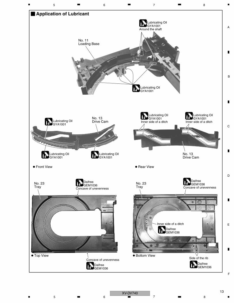
Application of Lubricant
Lubricating OilGYA1001
Around the shaft
No. 11 Loading Base
No. 23 Tray
No. 13 Drive Cam
No. 13 Drive Cam
No. 23 Tray
Front View Rear View
DaifreeGEM1036
Inner side of a ditch
Concave of unevennessTop View Bottom View
DaifreeGEM1036
DaifreeGEM1036
Side of the rib
Lubricating OilGYA1001
Concave of unevenness
DaifreeGEM1036
Concave of unevenness
DaifreeGEM1036
Lubricating OilGYA1001
Lubricating OilGYA1001
Lubricating OilGYA1001
Inner side of a ditch
Lubricating OilGYA1001
Inner side of a ditch
Lubricating OilGYA1001
XV-DV7405 6 7 8
C
D
F
A
B
E
XV-DV74014
1 2 3 4
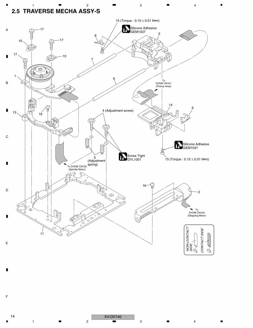
2.5 TRAVERSE MECHA ASSY-S
ToDVDM CN104
(Stepping Motor)
To DVDM CN105(Spindle Motor)
ToDVDM CN101(Pickup Assy)
CO
NT
AC
T S
IDE
NO
N-C
ON
TA
CT
S
IDE
3
7
8
1
17
16
17
10
13
17
10
6
11
14
16
2
9
15 (Torque : 0.15 ± 0.01 N•m)
15 (Torque : 0.15 ± 0.01 N•m)
4 (Adjustment screw)
5 (Adjustmentspring)
Screw TightGYL1001
Silicone AdhesiveGEM1037
Silicone AdhesiveGEM1037
1 2 3 4
C
D
F
A
B
E
15
5 6 7 8
TRAVERSE MECHA ASSY-S Parts List
Mark No. Description Part No.
1 Spindle Motor VXM1099
2 Stepping Motor VXM1101
> 3 Pickup Assy-S OXX8005
4 Skew Screw VBA1080
5 Skew Spring VBH1335
6 Guide Bar VLL1514
7 Sub Guide Bar VLL1515
8 Leaf Spring VNC1023
9 Joint Spring VNC1019
10 Support Spring VNC1020
NSP 11 Mechanism Chassis VNE2248
12 • • • • • •
13 Spacer VNL1913
14 Joint 03 VNL1949
15 Tapping Screw VBA1092
16 Screw BBZ20P050FTC
17 Screw PMA26P100FTC
XV-DV7405 6 7 8
C
D
F
A
B
E
XV-DV74016
1 2 3 4
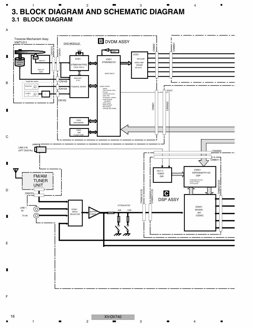
3. BLOCK DIAGRAM AND SCHEMATIC DIAGRAM3.1 BLOCK DIAGRAM
- 6dB - 10dB
system control
MPEGVideo Decoder VideoEncoder(withPictureControl)Video DAC(Progressive: 54MHz)Audeo Decoder -DD MPEGJPEG ViewerWMA PlaybackRW Playback(VRmode with CPRM)
IC602
64M SDRAM
IC603
16M
FLASH ROM
SPINDLEMotor
03SD PU
PlCK UPASSY
DVD MODULE
FTS&SPDL DRlVERSteppingtorM
+ -
VlDEO AMP
DRlVER
6IN-6OUT
M63018FPIC101
MM1623BF
L
20MHz
IC601
IC501
STM5589CVS
BACK END IC
27MHz
IC301
STM6316ATPAZFRONT END IC
LoadMotor M
+ -
*single disc mecha
DOUT
DolbyDigital DecoderDolby PrologicIIDTS Decoder
IC8501DSPD56367PV150
DSPIC8201
DIR
AK4114
IC3001INPUT
SELECTOR
IC8401AK4529
8chCODEC
LINE 1 IN
TV IN
LINE 2 IN
JA8602
(OPT DIGITAL)
BUFFERIC3003
ATTENUATOR
DVDM ASSYB
DSP ASSYC
FM/AMTUNERUNIT
Traverse Mechanism Assy VWT1211
CN5701
CN5620
CN8011
CN
5612
(1/2
)
CN
8007
(1/2
)
CN
8007
(2/2
)
CN
901
CN
101
CN
1013
CN103
CN105
CN104
CN
903
CN
5502
CN
8801
1 2 3 4
C
D
F
A
B
E
17
5 6 7 8
C
V
Y
B/Cb
R/Cr
G/Y
LPF
LPF
LPF
LPF
LPF
6ch E-vol
IC3062
JA3001
IC3901
IC3059
IC3056IC3057IC3058
BD3814FVE-VOL
IC3301
IC3401
STK402-270
STK402-270
3ch PowerAmp
Headphone
AMP
COMPOSITEVIDEO OUTS-VIDEOOUT
SW
Center
HEADPHONE OUT
FL/FROUT
SWOUT
CENTREOUT
SL/SROUT
microProcessor
IC5601FL
Driver IC
LINEOUT
ANDREW
FL Tube
IRSENSOR KEY
PDC114BIC5501
V5601
POWER AMP MODULE
SPEAKER RELAY
-
+
SW MIX/GAIN
FL/FR
SL/SR
REC OUT
COMPONENTVIDEO OUT
CONTROL ASSYF
POWER ASSY(1/2)J
DISPLAY ASSYM
6CH AMP ASSY
POWER ASSY(2/2)
HP ASSY
D J
I
CN
5612
(2/2
)
CN
3501
CN
5531
CN
3902
CN
3901
JA39
01
CN
5611
(2/2
)
CN
5611
(2/2
)C
N56
01(2
/2)
CN
3001
CN
3031
JA33
01
CN5611(1 /2)
CN5601(1/2)
VIDEO ASSYL
CN
8807
CN
8001
XV-DV7405 6 7 8
C
D
F
A
B
E
XV-DV74018
1 2 3 4
3.2 LOAB ASSY and OVERALL WIRING DIAGRAM
S5B
-PH
-SM
3
AK
N70
35
RK
N10
53
VK
N14
64
CN
1013
VK
N14
82
VK
N13
22V
KN
1261
B10P-VH
B2P3-VH
XKP3041
VK
N13
11V
KN
1249
21 3
1
4 5
21 3 4 5
2 3 4
1 2 3 4
8
511
6
9
1012
7
4
12
3
8
511
6
91012
7
4
12
3
20
11
22 18
19
16
17
14
15
12
13
24
10
2123
6 2
5 3
4
9
87 1
19
24 22
21
20
23
11
18 16
17
14
15
12
13
10
3
2
5
46
9
87 1
308
7
10
9
6
4
5
2
3
1
8
7
10
9
6
4
5
2
3
1
1
2
1
2
2
1
2329
28
27 25
2426 22
19
18 1416
17 15
21
20 10
1112
13 7
68
9 5 3
21
4
30 2228 2426 20 18 1416
2329 27 25 21 19 17 15
81012 6 4 2
91113 7 5 3 1
6
75
2
3
4
1
14
9 11
108
13
12
15
16
17
18
642 10 12 148
1 73 5 11 13 159 17
16 18C
N103
K-H
P-B
5SC
N601
CN
104
CN
105
CN
101
CN
901
CN
5102
CN11
CN2
AN1
CN
903
CN
8801
VKB1150JA8951
LOA
D+
SW
2
LOA
D-
ST
1-(A
)
SW
1(G
ND
S)
V+
3D
ST
1+(A
)
ST
2+(B
)
ST
2-(B
)
FF
C 1
2P A2
A1
A3
H1+
H1-
H2-
H2+
H3+
H3-
GN
DS
V+
5SIN
SID
E
TR
KG
DR
VT
RK
G R
TN
GN
DV
SH
F
FO
CS
DR
V
FO
CS
RT
N
24P
FF
C
DV
D V
RV
RE
F
CD
VR
LD2
LMD
LMD
GN
D
LD1
C B3
B4
AB1
B2
VC
C
OE
ICG
780/
X65
0
GN
D
VD
VD
+12
FLAC
FLAC
AC5V
AC5V
VL
VH
VL
GND
VH
VFDP
T1 XTS3075
NEUTRAL
LIVE
VP
R+
8
VP
R+
8(M
)V
PR
+8(
M)
VP
R+
8
DO
UT
(AC
3)
DV
DP
OW
ER
SY
S_C
S2
SY
S_C
S1
XD
VD
RS
T
GN
DD
GN
DM
GN
DM
GN
DD
GN
DD
GN
DD
SC
LK
DV
DA
CK
TR
KU
PD
VD
MU
TE
MD
AT
AS
DA
TA
XV
MU
TE
GN
DD
GN
DD
VD
ET
CT
SR
TS
TX
DR
XD
GN
DD
VD
VD
+12
VP
R+
8
VP
R+
8(M
)
GN
DD
VP
R+
8(M
)
GN
DM
GN
DM
VP
R+
8
XD
VD
RS
TS
YS
_CS
1S
YS
_CS
2S
CLK
DO
UT
(AC
3)
GN
DD
GN
DD
DV
DP
OW
ER
TR
KU
PD
VD
MU
TE
MD
AT
AD
VD
AC
KG
ND
DG
ND
DV
DE
T
SD
AT
A
RT
SC
TS
XV
MU
TE
TX
DR
XD
AS
PE
CT
LET
TE
RS
QU
EE
ZE
RG
B
P/X
I
VS
EL1
VS
EL2
GN
DV
Cr/
RG
ND
V
Cb/
BG
ND
VC
Y/G
GN
DVC YV
GN
DV
AS
PE
CT
LET
TE
RS
QU
EE
ZE
VS
EL2
VS
EL1
RG
BP
/XI
C GN
DV
GN
DV
Cr/
R
Cb/
BG
ND
V
GN
DV
CY
/G
V YGN
DV
FAN
PICKUP ASSY-S (OXX8005)
DVD ASSY (AXA7131)
ST
EP
PIN
GM
OT
OR
: VX
M1101
LOA
DIN
G M
OT
OR
AS
SY
: VX
X2912
CN
602
SP
IND
LE M
OT
OR
: VX
M1099
5204
5-05
45
4
3
2
1 5
5
4
3
2
1
41 32 65
CN
8807
Cb/
BG
ND
V
Cr/
RG
ND
V
5pin
FF
C
CY
/G
CbY
YG
ND
CrG
ND
CbG
ND Cr
CN
8001
5204
5-05
45
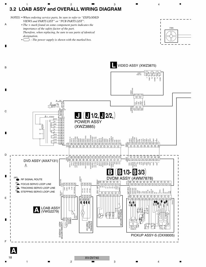
: RF SIGNAL ROUTE
: FOCUS SERVO LOOP LINE
: TRACKING SERVO LOOP LINE
: STEPPING SERVO LOOP LINE
(F)
(RF)
(T)
(S)
(RF
)
(RF
)
(RF
) (RF
)
(RF
)
(RF
)
(F) (F
)
(T)
(T)
(S)
(S)
(S)
(S)
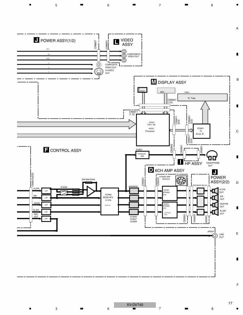
J 1/2, J 2/2,JPOWER ASSY(XWZ3885)
LOAB ASSY(VWG2279)A
B 1/3- B 3/3BDVDM ASSY (AWM7878)
A
NOTES: • When ordering service parts, be sure to refer to “EXPLODED VIEWS and PARTS LIST” or “PCB PARTS LIST”.
• The > mark found on some component parts indicates the importance of the safety factor of the part.Therefore, when replacing, be sure to use parts of identical designation.
• : The power supply is shown with the marked box.
VIDEO ASSY (XWZ3875)L
1 2 3 4
C
D
F
A
B
E
19
5 6 7 8
AK
P70
70A
KP
7059
AK
P70
73A
KP
7062
AK
P70
73A
KP
7062
AK
P70
58A
KP
7069
AK
P70
62-
AK
P70
73-
XKN3015
AKP7050
AK
P70
62-
AK
P70
73-
52044-154552045-1545
52045-0545 52044-0545 AKN7003
TORX179PL
AK
P70
64A
KP
7075
AK
P70
75
AK
P70
64A
KP
7075
AK
P70
75
AK
P70
64
VK
B11
22
AK
P71
79
AK
P70
64
AK
P70
64A
KP
7064
52045-1145
VK
N12
67
AK
P70
75A
KP
7075
KM200SA2
AK
P70
75A
KP
7075
XKE3021
AK
P70
64
1113
10
9
12 487
65 1
2
3
1113
10
9
12 48
7
6
5 1
2
3
6
12
3
4
5
8 1211
14
137 9
10
1216
15
18
17 19
6
12
3
4
5
8 1211
14
137 9
10 16
15
18
17 19
78
9
104
56
3
1211
18
17
14
13
16
15 19
12
78
9104
56
3
1211
1817
1413
1615 19
10
911
10
321
911
268 4
26
5
8
7
4
3 1 19
1416
15
18 1416
18
17
57 3 1
1719 15
10
13
8
9
10 6
7
61212
11
8 4
2 18
193
4
5
18
12
791113 35 191
12
17
14
13
16
15
1214
11
16 1010
128
3
4
56
287
4
9
6
15 1117 13 7 19 35
14
15 12
13
9
1211
8
10 6
8
4
5
3
7
6
2
4
7
3
5
13
9
1211
10
14
151
3
5
4
5
4
3
2
1 1
2
3
4
5
2
1
21 3
1
1
56
78
9
4
3
2 16
15 171112
13
14
10
56
78
9
4
3
2 16
15 171112
13
1410
22
21 23
18 2019
4
3
21
65 7
8
22
21 23
18 2019 5 7
84
3
21
6
16
10 14
1112
13 159
22
21 23
18
17
2019
1112
13
14
9
10 16
15
2019
22
21 23
18
17
1
1 9
6
4
3
2
78
9
4
3
2
5
56
78 10
1112
13
1410 16
16
15
17
17
15
1112
13
14
23
19
22
21 23
18 20
22
21
18 2019
8
3
21
1
6
7
4
3
2
5
4
8
56
7 9
10
1112
13 159
10
16
15
16
1112
13
14
14
17
2019
20 22
21 23
18
17 19
22
21 23
18
2
65
4
3
1
9
11
87
10
2
65
4
3
1
9
11
87
10
21
4
3 7
65
11
1
56
78
9
4
3
2
56
78
9
4
3
2
16
15 171112
13
1410
16
15 171112
13
1410
56
78
9
4
3
2 16
15 171112
13
1410
1
2
23
1818
2020
21 23
19
22
19
22
21
1 56
78
5
4
3
2
784
3
21
6
22
21 23
18 2019 5
6
78
3
2 4
1
139
15
16
15
1112
13
14
910
1112 1410
16 22
21 23
18
17
2019
22
21 23
18
17
2019
1112
13
10 14
9
16
15 19
18
17
20 22
21 23
6 84
1 73
2
5 1112
13
10 16
9 15
14
1917
20
23
22
21
18
CN
5615
CN
5614
CN
8007
CN
8003
CN
5618
CN
8011
CN
5613
CN
5617
CN
5616
CN
5612
JA8803
JA3001
CN
5620
CN
5619
CN5601CN5611
CN3902 CN3901 JA3901
JA8602
CN
5501
CN
5511
CN
5502
CN
5512
CN
5522
CN
5531
CN
5521
JA88
03C
N88
02
CN
5532
CN5701
CN
8003
CN
3021
CN
3031
CN
3011
CN3501
CN
3022
CN
3032
CN
3012
JA3301
CN
3002
VD
+5
GN
DD
*
V+
5A
GN
DA
(DA
)
GN
DA
(DA
)
DO
UT
GN
DLE
D
GN
DU
VD
+5
GN
DD
GN
DD
DIN
AC
3IN
FR
O
GN
DA
(IN
)
VC
OM
G
LIN
GN
DA
(IN
)
RIN
GN
DC
SR
O
SW
O
GN
DC
SLO
RE
CM
UT
EF
LO
GN
DC
GN
DCC
GN
DC
GN
DD
NC
SB
LO
SB
RO
DS
PM
OD
E
DS
PH
RE
Q
BU
SY
XT
LO
DIR
CS
DIR
DO
DIR
ER
R
DIR
RS
T
DS
P M
UT
E
DS
PC
LK
DE
CM
UT
E
MO
DC
DS
PD
O
DS
PD
I
DS
PS
S
DS
PR
ST
MU
TE
OU
T
SR
PLU
S
GN
DA
(DA
)V
+5A
VD
+5
DO
UT
GN
DU
VD
+5
GN
DD
GN
DD
GN
DD
1
DIN
AC
3IN
FR
O
VC
OM
G
RIN
LIN
GN
DC
(IN
)
GN
DC
(IN
)
SLO
SR
O
FLO
RE
CM
UT
E
GN
DC
GN
DC
GN
DC
SW
O
NC
SB
LO
SB
RO
GN
DC
GN
DD
GN
DC
CO
BU
SY
DIR
RS
T
DIR
CS
DIR
DO
DS
PM
OD
E
DS
PH
RE
Q
XT
LOD
IRE
RR
DS
P M
UT
E
DS
PD
I
DE
CM
UT
E
MO
DC
MU
TE
OU
T
DS
PS
S
XD
SP
RS
T
DS
PC
LKD
SP
DO
R
R
L
L
LIN
E1
LIN
EO
UT
R
L
TV
15pinFFC
GND LED
NC
TIMERLED
VE+5
FLAC2
FLAC1
KEY1
REMOCON
XFLRST
FLCSFLCK
FLDATA
VFL+5
GNDFL
VFDP
HP MUTEHP DET
HP R
5pinFFC
HP LGNDA
OP
T IN
DIG
ITA
L
VP
R+
8(V
D+
5)
SY
S_C
S1
SY
S_C
S2
WA
KE
UP
HP
AC
RY
FS
C
RY
RV
D+
5
AC
K
VX
+12
GN
DX
VA
-12
VA
+12
FR
IN
GN
DA
GN
DA
FLI
N
DV
DM
UT
E
XD
VD
RS
T
DV
DO
N/O
FF
SY
SP
OW
XP
RO
TE
CT
SR
IN
CIN
SLI
N
VE
+56
SW
IN NC
GN
DD
GN
DD
GN
DD
DO
UT
GN
DU
SU
BA
C
VE
+56
MU
TE
GN
DF
L
VF
DP
VF
L+5
MU
TE
C
FLA
C1
FLA
C2
SD
AT
A
VD
ET
SC
LK
MD
AT
A
OU
TV
IDE
O
HP
AC
RY
R
GN
DX
VX
+12
VD
+5
RY
FS
C
VP
R+
8(V
D+
5)
DV
DO
N/O
FF
XP
RO
TE
CT
GN
DA
GN
DA
FLI
N
MU
TE
C
MU
TE
VA
+12
VA
-12
FR
IN
S-V
IDE
OO
UT
Exc
ept
/MY
XJ,
/NV
XJ
VH
-
SW
OU
TS
WO
UT
GN
DS
FLO
UT
VL+
GN
DP
VL+
SR
OU
T
CO
UT
GN
DP
FR
OU
T
FLO
UT
FR
OU
T
VH
+V
H+
VH
-
CO
UT
NC
DV
D M
UT
ES
RIN
SLI
NS
WIN
CIN DO
UT
GN
DD
GN
DD
GN
DD
GN
DU
VE
+56
SU
BA
C
NC
VF
DP
GN
DF
LV
FL+
5
VD
ET
WA
KE
UP
FLA
C1
FLA
C2
SY
SP
OW
MD
AT
AS
DA
TA
SC
LKS
YS
_CS
2S
YS
_CS
1X
DV
DR
ST
AC
K
XP
RO
TE
CT
GN
DF
SLO
UT
VL-
SLO
UT
SR
OU
T
TU
NE
R
VL-
GN
DR
EG
VD
+5
UN
+8V
GN
DR
EG
UN
+8V
SLI
N
MU
TE
SW
IN
FLI
NG
ND
A
VP
R+
8V
PR
+8
VP
+15
VF
L+5
SR
IN
VA
-12
CIN
GN
DA
FR
IN
MU
TE
C
TXLGND
CLK
DO
DI
CE 11pinFFC
RDS
+9V
TXR
VSM
GND
-SR
SL+
+
-
FR
SW
-
+
+
-
FL+
-
C-
+
6ch SPEAKER OUT
RX
DT
XD
RT
SC
TS
DVD DOWNLOAD
NC
VD
+5
GN
DD
DT
R
AK
P70
64
1V
H-
CN
3001
FAN+
FAN-
FLO
UT
GN
DP
FR
OU
TF
RO
UT
VH
-
GN
DS
8
GN
DP
7F
LOU
T
9
2 4 6
3 5
VL+
CO
UT
VH
+
VL+
CO
UT
17
SW
OU
T
12 14 16
13 15
10
11S
WO
UT
VH
+
SR
OU
TS
RO
UT
SLO
UT
VL-
VL-
22
23
18 20
SLO
UT
19 21
VD
+5
TU
NE
R
GN
DF
UN
+8V
XP
RO
TE
CT
GN
DR
EG
GN
DR
EG
UN
+8V
VF
L+5
VP
+15
VA
-12
SE
NS
E+
8M
UT
EC
FLI
NM
UT
E
GN
DA
SR
IN
FR
IN
VP
R+
8
CIN
VP
R+
8
SW
INS
LIN
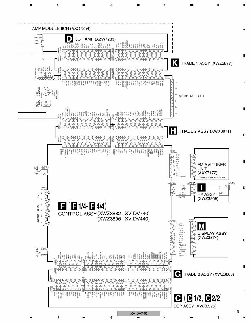
F 1/4- F 4/4FCONTROL ASSY (XWZ3882 : XV-DV740)
(XWZ3896 : XV-DV440)
AMP MODULE 6CH (AXQ7254)
6CH AMP (AZW7283)D
FM/AM TUNER UNIT(AXX7172)
HP ASSY(XWZ3869)
I
DISPLAY ASSY(XWZ3874)
M
TRADE 1 ASSY (XWZ3877)K
TRADE 2 ASSY (XWX3071)H
C 1/2, C 2/2CDSP ASSY (AWX8526)
G TRADE 3 ASSY (XWZ3868)
* No schematic diagram
XV-DV7405 6 7 8
C
D
F
A
B
E
XV-DV74020
1 2 3 4
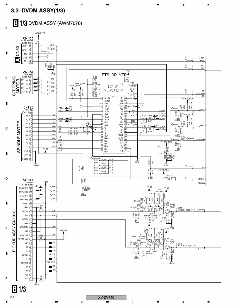
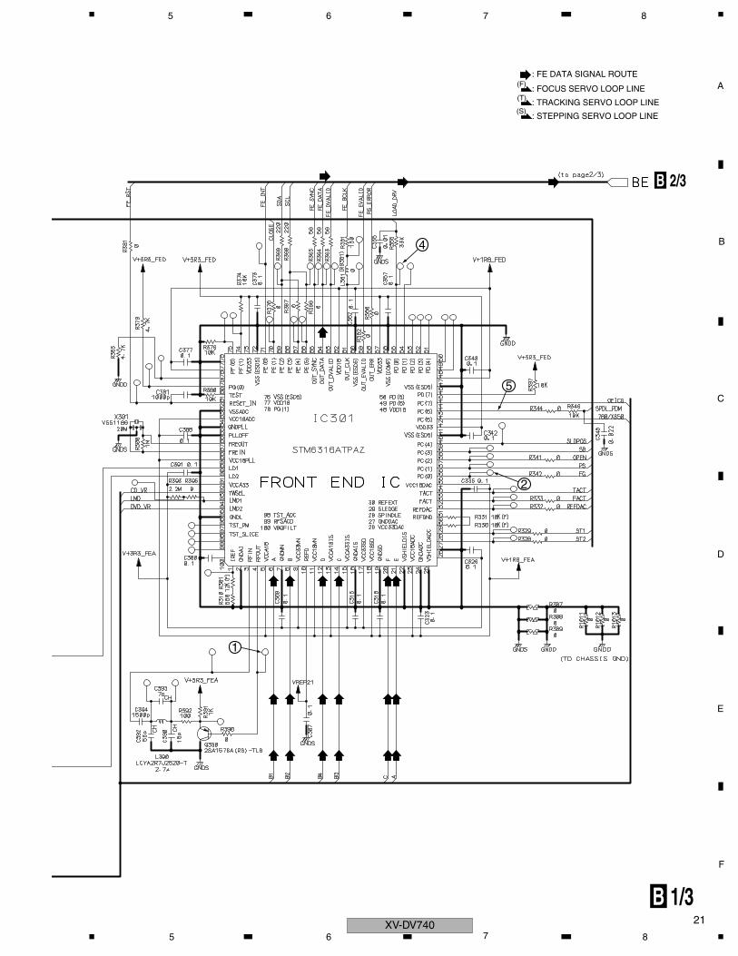
3.3 DVDM ASSY(1/3)
B 1/3
B 1/3C
N60
1S
TE
PP
ING
MO
TO
RP
ICK
UP
AS
SY
CN
1013
DVDM ASSY (AWM7878)A
SP
IND
LE M
OT
OR
3
(F)
(F)
(T)
(T)
(S)
(S)
(S)
(S)
(S)(S)
(S)(S)
(F)(F)
(T)(T)
1 2 3 4
C
D
F
A
B
E
21
5 6 7 8
B 2/3
B 1/3
1
2
4
5
: FOCUS SERVO LOOP LINE
: TRACKING SERVO LOOP LINE
: STEPPING SERVO LOOP LINE
(F): FE DATA SIGNAL ROUTE
(T)
(S)
XV-DV7405 6 7 8
C
D
F
A
B
E
XV-DV74022
1 2 3 4
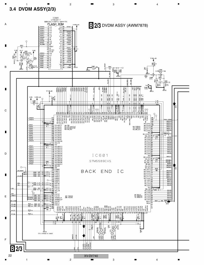
3.4 DVDM ASSY(2/3)
B 2/3
B 2/3 DVDM ASSY (AWM7878)
(Y)
(C)
(C/V
)
(D)
(D)
(D)
(CY
/G)
(PR
/R)
(PB
/B)
1 2 3 4
C
D
F
A
B
E
23
5 6 7 8
B 2/3B 1/3
B 3/3
B 3/3
B 3/3
6
7 8
9
10 11
: FE DATA SIGNAL ROUTE
: S VIDEO SIGNAL ROUTE (Y)(Y)
: S VIDEO SIGNAL ROUTE (Y)(C)
: VIDEO SIGNAL ROUTE (C/V)(C/V)
: AUDIO SIGNAL ROUTE (DIGITAL)(D)
(D) (D) (D)
(Y) (Y)
(Y)(Y)
(C) (C)
(C)
(Y)
(C/V
)
(C)(C)
(C/V) (C/V)
(C/V)
(C/V)
: VIDEO SIGNAL ROUTE (CY/G)(CY/G)
: VIDEO SIGNAL ROUTE (PR/R)(PR/R)
: VIDEO SIGNAL ROUTE (PB/B)(PB/B)
(CY/G)
(CY/G)
(PR/R)(PR/R)
(PB/B)
(PB/B)
(CY/G)
(PR/R)
(PB/B)
XV-DV7405 6 7 8
C
D
F
A
B
E
XV-DV74024
1 2 3 4
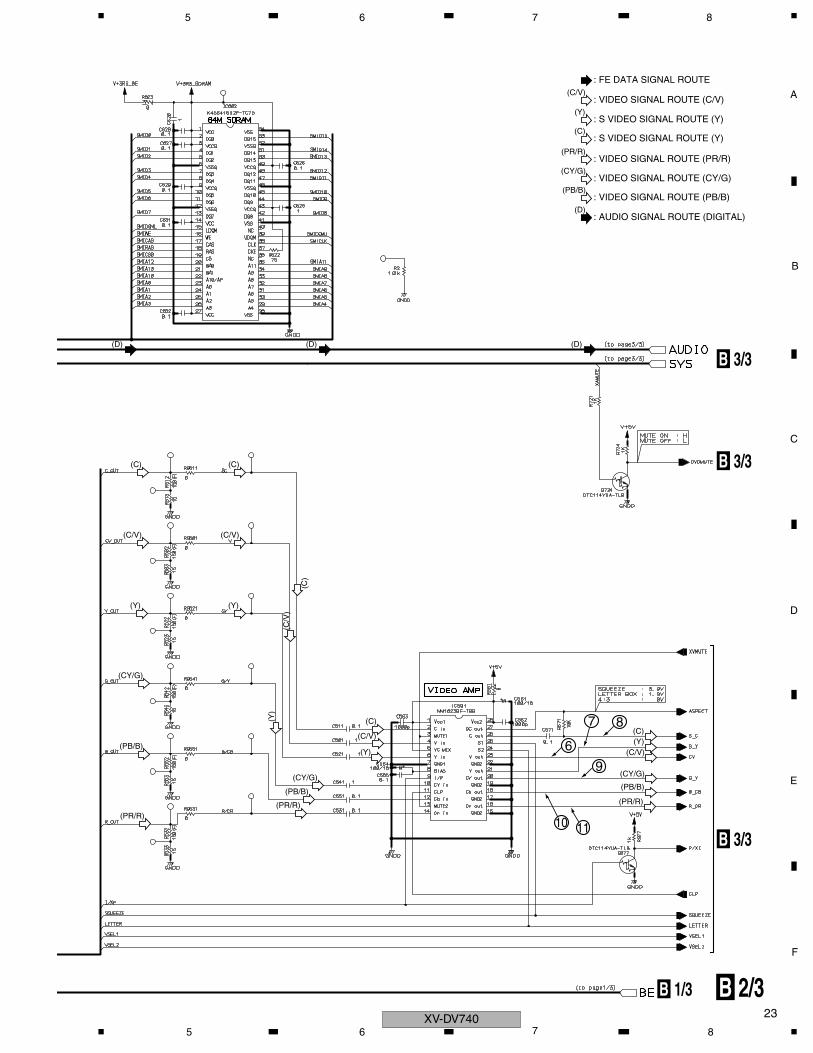
3.5 DVDM ASSY(3/3)
B 3/3
B 3/3 DVDM ASSY (AWM7878)
B 2/3
1.8V Reg.
1.8V Reg.
(D) (D) (D)
1 2 3 4
C
D
F
A
B
E
25
5 6 7 8
B 3/3
B 2/3
B 2/3
CN
5102
J1/2
CN
8801
J2/2
5V Reg.
: S VIDEO SIGNAL ROUTE (Y)(Y)
: S VIDEO SIGNAL ROUTE (Y)(C)
: VIDEO SIGNAL ROUTE (C/V)(C/V)
: AUDIO SIGNAL ROUTE (DIGITAL)(D)
: VIDEO SIGNAL ROUTE (CY/G)(CY/G)
: VIDEO SIGNAL ROUTE (PR/R)(PR/R)
: VIDEO SIGNAL ROUTE (PB/B)(PB/B)
(Y)
(C)
(C/V)
(CY/G)
(PR/R)
(PB/B)
(Y)
(C)
(C/V)
(CY/G)
(PR/R)
(PB/B)
(Y)
(C)
(C/V)
(CY/G)
(PR/R)
(PB/B)
(D) (D)
(D) (D)
XV-DV7405 6 7 8
C
D
F
A
B
E
XV-DV74026
1 2 3 4
3.6 DSP ASSY (1/2)
GNDD100k
100k
100k
0
00
0
0
QTL1013
CH
470p
47/6
.3
YB
0.1
V53V5D1 V3D
QTL1013
CH
470p
YB
0.1
GNDD
stby0stby
V32
100k
100k
100k
GNDD
0
stby
stby
0
AK4114VQ
47 100
GNDD
100
100
stby
0
10p
GNDD
CH
10p
CH
47
0
stby
XSS300324.576MHz
stby
100
0
100
10k
18k
0.47
YB 10
00p
stby
100
YB
stby
CH
470p
47/6
.30.
1 GNDD
YB QTL1013
YB
0.1
V31 V3D
R8321
R8320
R8322
R8340
R83
34R
8328
R83
38
R83
39
C82
12
C82
25
C82
13
L8203L8204
L820
5
C82
14
C82
15
C82
16
R82
19
R81
14
R81
13
R81
15
R82
23
R82
22
R8221
R8220
IC8201
R82
13
R82
14
R82
15 C82
11
C82
09
R8216 C82
10
R8209
R8225
R8204
L8202
X8201
R8210
R8207
R8206
C82
04
R82
02
R82
01
C82
03
C82
01
C82
06
R8205
C82
05
R8203
C82
07
C82
02
C82
17
L8201
IE
LOC
K
ER
R
LCKI
MCLK
IEIT
IEDO
PWR
12
1413 171615
9
8
10
11
5
4
7
6
22201918 2321
25
24
29
27
26
28
31
33
30
32
3
1
2
45464748 44 40414243 39 38
35
34
37
36
DV
SS
VINT
VD
D BO
UT
TX
1
TX
0
XTL1
P/SN
XTL0
IIC
AVSS
RX6 DIR&DITAVSS
RX7
MC
KO
1
DV
DD
VO
UT
UO
UT
CO
UT
DV
SS
SDTO
LRC
K
XTO
DAUX
BICK
MCKO2
CDTI
PDN
XTI
CDTO
RX
1
AV
SS
RX
3A
VS
S
RX4 RX
2
AVSSRX5
VC
OM
AV
SS
RX
0
AV
SS
AV
DDR
CSN
INT0
CCLK
INT
1F%
KN8102VNF1084
GCH
stby
0R8233
C8208
100
R82
12
stby
0
C8226
R8229
AC 1/2
(D)
(D)
(D)
(D)
(D)
(D)
1 2 3 4
C
D
F
A
B
E
27
5 6 7 8
GNDD
YB 0.1
GDAC GNDD
stby
GCH
0.01YB
CH 470p
CH 470p
AKP7070
stby
AT
L700
2
stby
AT
L700
2
stby
0 GNDD
stby
0
0
0
0
stby
stby
GNDD GCH
stby
stby
GCH
0.1
YB
GNDD
100/
16
V5D1
NJU7223DL1-18
V1R8
GNDD
V5A
0
CH
YB
100/
16
YB
470p0.01
QT
L101
3
GDAC
YB
V5D1
GVCM
0
stby
100p
CH
0.1
4.7
stby
stby
stby
100CH
CH470p
V3D
V34 V55
100
47st
by
stby
GDAC
stby
100
100
CH470p
470p
470pCH
470p
CH470p
CH
100
100
100
AK4529VQ0
DA
P20
2K 470p
CH470p
100
100
CH
DA
N20
2K
0.1
YB
NJM2391DL1-33
V5D1
100/
16
V3D
0
100
100
100
47
YB
0.1
47/6
.3
GVCM
GDAC
470p
CH
0.01
YB
V54
QT
L101
310
0/16
V5A
AK
P70
73
C8010
C8009
C8008
CN8003C8007
R80
02
L800
2
R80
04
R80
14
R8015
L800
4
R80
05
L800
5 R8011
R80
13
R8019
C8006
C8014
C8013
C8011
C8012
C89
03
C89
04
IC8902
R8006
C84
19
C84
18
C84
15
R8417
C84
20
L840
2
R8010
C8004
C84
21
C84
22
R8415
R8009
C8001
C8002
R8416
C8417
R8406
R8405
C84
02
C84
01
C84
03
R8413
C8416
C8414
R8410
R8411
R8414R8412 C8413
C8412
IC8401R8407
D84
02
R8408
R8409 C8411
C8410
C8409
C89
01
C89
02
IC8901
R80
17
R8402
R8403
R8401
R84
04
C84
07
C84
08
D84
01
C84
04
C84
05
L840
1C
8406
CN
8007
BCKI
FDTI
XTL0
DRRT
DATA
DRRTDRDO
CLK
LOCKDRCS
BDTO
CDTO
FDTO
BCKOLCKO
SDTO
MC
MD
DATA
DRCS
CLK
MCLK
OUTIN
OUTIN
12 10
13 11 56
9 78 4
3
21
123
1312
118
910
45
67
3
4344
12
15 17 191614 18 20 2221
2326
2425
3028
3127
29
38394041 3742 34
33
36 35
32
1 2
3
2 1
1 32
17
18
19
15
16
13
14
12
8
11
10
9
4
7
65
3
12
3
NOTES:
UNLESS OTHERWISE NOTED
RS1/16S***J-T
CKSRYB333K16-TCKSRYB104K16-T
CEV***M**-T
CKSRYB105K6R3-T
CCSRCH****50-TCKSRYB****50-T
NO INDICATED PARTS IS...
GN
DD
(13
94)
GN
DA
(D
AG
)G
ND
A (
DA
G)
V+
5A
OP
TIN
or
DG
RT
N
OP
TIN
or
uGR
TN
OP
TO
UT
or
uGR
TN
GN
DD
DG
RT
N
uGR
TN
V+
5DV
+5D
GN
DD
(DSP) (DSP)
VNF1084KN8501
stby
(DIR)
VNF1084KN8201
stby
stby
0.1
SDTI4
DFSD
ZF
E
SDTI2
SDTI3
SDTO
DAUX
SMUTE
BICK
LRCK
SDTI1
CD
TI
TD
M
SDOS
I2C
PD
N
CA
D1
TV
DD
DV
DD
TS
T
DV
SS
RO
UT
4
LOU
T4
LOUT3CA
D0
8ch CODEC
ROUT3
LOUT1
LOUT2
ROUT2
or AK4628VQ
LINNC
NC(TST)
ROUT1
AV
SS
DZ
F1
MC
LKP/S
CS
N
CC
LK
DZF2/OVF
RIN
VC
OM
AV
DD
VR
EF
H
SBROGNDA(DAG)SBLO
GNDA(DAG)
GNDA(DAG)
GNDA(DAG)CO
SWO
SLO
RECMUTE
GNDA(DAG)SRO
VCOMGFLO
GNDA(DAG)FRO
GNDA(DAG)LIN
RIN
C 1/2
C 1/2
DSP ASSY(AWX8526)
G
G CN5615
CN
5614
: AUDIO SIGNAL ROUTE (DIGITAL)(D)
: AUDIO SIGNAL ROUTE (DVD Lch)(DVD)
: AUDIO SIGNAL ROUTE (L ch)
: AUDIO SIGNAL ROUTE (Front L ch)(FL)
: AUDIO SIGNAL ROUTE (Surround L ch)(SL)
: AUDIO SIGNAL ROUTE (Center ch)(C)
: AUDIO SIGNAL ROUTE (Sub Woofer ch)(SW)
: AUDIO DATA SIGNAL ROUTE(AD)
(D)
(D)
(D)
(D)
(AD)
(AD)(AD)
(AD) (FL)
(SL)
(C)
(SW)
(DVD)
(DVD)
XV-DV7405 6 7 8
C
D
F
A
B
E
XV-DV74028
1 2 3 4
3.7 DSP ASSY (2/2)
MU
TE
IEC
K
IE
IER
TIE
DI
DA
TA
MU
TE
MO
DC
DS
DO
DR
DO
ER
R
DS
RQ
LSSN
1394
DS
RT
DS
SS
CLK
DS
MD
XT
L0
DR
CS
DR
RT
MC
LSS
N
BCKOLCKI
LCKO
BCKI
IED
I
IEC
K
MO
DC
IEIT
DS
MD
IED
O
BDTO
MCLK
FDTI
SDTOFDTO
CDTO
MD
DS
SS
DS
RT
CLK
DA
TA
IEC
K
IED
IDSRQ
DSDO
GNDD
GNDD
1M 1M 10k
1M
DA
P20
2K
UMD2N
DA
P20
2K
UN5112
UMD2N
1SS355
V3D
100k
100k
100k
100k
100k
GNDD
330
330
CH
10/1
6
YB
0.1
QT
L101
3
TC74VHCT244AFT470p
100k
100k
100k
100k
100k
100k
GNDD
0
100k
100
YB
1000
p
YB
0.1
100
CH470p
100
47k
47k
10k
4.7k
470p CH
4.7k
GNDD
100
V56V5D1
330
330
330
330
GNDD
10/1
6
YB
0.1
CH TC74LVX244FT
470p
V38
QT
L101
3
CH
47k
470p
470p
CH
47
47
10k YB
47
47
CH
470p
0.1
47
RA
B4C
101J
100
10k
10k10k
10k
100
stby
stby
100
stby
4.7k
0
47k
V3D
100
10k
V3D
R85
38
R85
48
R85
47
R85
49D
8503D85
02
Q8503
Q8504
Q8504
D8501
R88
12
R88
11
R88
13
R88
01
R88
10
R87
04
R87
03
C87
04
C87
05
C87
06
L870
2
IC8702
R88
03
R88
05
R88
02
R88
04
R88
07
R88
06
R8809
R88
08 C85
55
R8526
R85
58
R85
20
R85
21
C8512
C8513
R8519
R8518
R8517
R8516
C85
11
R85
22
R87
07
R87
05
R87
08
R87
06
C87
03
C87
02
C87
01 IC8701
L870
1
R8515
C85
09C
8507
R8514
R85
09
R85
07
R85
08
R8557
C85
04
R85
10
R8513
R8512
R8511
C85
05
R85
06
R8505
R8503
C85
01
C85
02
C85
03
R8504
R85
55
R85
32
R8502
R8501
R8534 TP5 TP2TP3TP4 TP1
2 1 2 1
C E
3 B
E
C
1
3
B2 B
E2
2
C2
541 32
10
76 98
20 18 17 1619 13 12 111415
36
4237 39 414038
34
35
33
32
31
30
29
28
27
26
25
24
43 44
43 51 2 76
10
98
1720 1619 18 15 14 13 12 11
23
20
21
22
19
16
17
18
14
13
12
15
7
10
8
9
3
6
5
4
2
1
143 141142 140139144 137138
11
DE
C M
UT
E
MU
TE
OU
T
DS
P D
I
MO
DC
MU
TE
DS
P H
RE
QD
SP
MO
DE
DS
P D
O
DS
P R
ST
DS
P S
SB
US
Y
DS
P C
K
DIR
RS
T
DIR
DO
DIR
CS
DIR
ER
R
GN
DD
XT
L0LS
SN
(1/2)6
5
(2/2)
4
2Y4
1A1
1G 1A2
GN
D2Y
1
2Y3
2Y2
1A3
1A4
Level shifter
2A4
VC
C
1Y1
2G 2A2
1Y3
2A1
1Y4
1Y2
2A3
BUSY PB5P
B4
VC
CH
PB
2P
B3
GN
DH
PB
1
PB9PB8PB7PB6
96DTS
LSS
N
1394
PB10PB13
ACI
TIO0
VCCS GNDS
PB15PB14
ADO
1
2
3
PB
0
RE
SE
TAD
MD
1A2
2Y3
2Y4
1G 1A1
1A3
1A4
2Y1
GN
D
2Y2
Level shifter
5V 3V
5V 3V
1Y1
2GVC
C
1Y2
2A4
2A2
2A1
1Y4
1Y3
2A3
L ON
H HI-Z
G Y
VCCQH PB12
GNDQ
PB11MUTE
HCKTSCKR
VCCQLHCKR
SDI0 FST
SCKTFSR
SDO3VCCSGNDSSDI1
96DTSMODEL
OTHERS
USE
NO USE
USENO
USE
IC8503L8505R8544R8545R8546
R8543R8542C8552
C8553
SDO1SDO0HREQ
SDO2
SS
SCK
TD
I
MIS
O
MO
SI
TM
S
TD
O
TC
K
JTAG
SD
I1_1
M
OD
A
0
R8542
R8543
0
AKP7073CN8011
1517
18 16
19
10
13
14
1112 6
5
4
9
87
213
AC 2/2
G CN5618
1 2 3 4
C
D
F
A
B
E
29
5 6 7 8
AA
1A
A0
WR
RD
RD
A0 A1
A3A2
A6
A4A5
A9A8A7
A10A11
A12
A14A13
A15A16
A17
D1D2
D0
D23
D20D21
D22 D16
D18
D19
D17
D12
D14
D13D15
D4
D3D
11 D8
D10 D
9 D6D7
D5
MR
CH
VSS1171
8p
CH
GNDD
TC7WU04FU
8p
CH470p
100
1M
470
TC7WU04FU TC7WU04FU
YB 0.1
V37
YB 0.01
QT
L101
3
YB 47
stby0.01
YB
0.03
3
1
YB
CH470p 0 CH
470p
YB
0.10.1
YB
0.1
470pCHCH
470p
47k
CH470p
47k
YB
47k
CH
470p YB
0.1
CH
470p YB
0.1
470p
DSPD56367PV150
CH
CH
YB
0.1
470p
0.1 YB
CH Y
B0.
1
470p
CH CH CH470p
YB0.1
0
YB0.1
470p 470p
0.1YB
CH
CH
YB
0.1
470p
470p
0.1YB GNDD
stby
AT
L700
2
100/
16
stby
100/
16
AT
L700
2
stby
V11 V36
V1R8 V3D
C85
48R
8540
X8501
C85
49
IC8502
R8541
IC8502
R8539
IC8502
C8551
C8550
C8554L850
4
R85
24
R85
27
C85
17C
8514
C8516
C8515
R85
52
C8518 C8522C8520
C8521 C8523 R85
29
C8525
C8524
R85
28
R85
30
C85
26
C85
27
C85
28C
8530
C85
29C
8531
IC8501
C85
32C
8534
C85
33C
8535
C8543C8545
R85
31
C8542C8544
C8541
C8540
C85
36
C85
37
C8539
C8538
R85
51
L850
1
R85
36
C85
46
L850
2
C85
47
R85
37
1
7
2
14
8
46 52 8
438
46 4745 50 51 52 5348 49 5854 55 595756 63626160 6564 6966 67 70 7168 72
73
74
75
76
77
79
80
81
78
82
83
84
85
87
88
86
89
92
91
93
90
96
97
94
95
98
100
102
101
99
135134136 128130133 129132131 122127126 124125 123 117118119120121 116
103
106
104
105
114115 112111110113 109
108
107
20MHz
(3/3)
(2/3) (1/3)
AAC&96DTS&MCACC
AAC&96DTSMCACC NO
USE
USEUSE
BASIC MODEL USENO
L8602C8608C8607C8606
NO
L8601C8604C8603C8602
USE USE
USE USE
NO USEUSEUSE
USE
USEUSE
L8603C8610
NO USE USENO
SD
I0_1
G
ND
P
VC
CP
PC
AP
CA
SS
CK
T_1
VC
CQ
H
FS
T_1
AA
2
GN
DC
FS
R_1
VC
CQ
LE
XT
AL
GN
DQ
VC
CC
TA
BB
VC
CC
PIN
IT
BRSC
KR
_1
BGWR
AA
0A
A1
GN
DC
RD
VCCAGNDA
VCCAGNDA
VCCA
C8601IC8601
C8605IC8602
C8609IC8603 R8523
(AX6)
DSP
UCOMP2ROM
01 01 0
10 0
GNDA
GNDQ
VCCQL
VCCQHGNDA
DECORDERBOOT MODE A B C D
0 1 0 0
MO
DC
MO
DB
MO
DD
GN
DD
VC
CD
GN
DQ
VC
CQ
L
GN
DD
VC
CD
GNDDVCCD
GN
DD
VC
CD
1394MCACC 10K
BASICMODELDVD-A
10KR8534
0Ω
0Ω
0Ω
0ΩR8531 R8533 R8550 R8551
UN5212
Q8501
0
R85
33C 2/2
C 2/2
DSP ASSY(AWX8526)
XV-DV7405 6 7 8
C
D
F
A
B
E
XV-DV74030
1 2 3 4
3.8 6CH AMP ASSY
Non Distortion Circuit
2
3
5
D
CN
3011
KC
N30
12K
CN3651
CN3001
CN3002
to FAN Motor
6CH AMP (AZW7283)D
(SL)
(FL)
(SW
)
(C)
(SL)
(FL)
(SW)
(C)
1 2 3 4
C
D
F
A
B
E
31
5 6 7 8
D
at SEARCH : 2.3AAT NORMAL : 950mA
30PDA20-FC6
30PDA20-FC6
(C)
(FL)
(SW)
(SL)
: AUDIO SIGNAL ROUTE (Front L ch)(FL)
: AUDIO SIGNAL ROUTE (Surround L ch)(SL)
: AUDIO SIGNAL ROUTE (Center ch)(C)
: AUDIO SIGNAL ROUTE (Sub Woofer ch)(SW)
: Refer to "7.3.2 PROTECTION CIRCUIT.
XV-DV7405 6 7 8
C
D
F
A
B
E
XV-DV74032
1 2 3 4
3.9 CONTROL(1/4), TRADE3 and TRADE2 ASSYS
CN5618 CN5619 CN5620
C5800
CN5614 CN5616 CN5612
C57
99
C55
71
Q5571 C55
79
C5576
C55
77C
5575
R5571
R55
72
C55
72
R3180
C55
73
C55
74
R55
73
L5571
R55
75
Q5572
C55
78
R5577
R55
74
R5576
D5575
R3280
Q5501
R55
81
R55
60
R55
62
R55
61
R55
31
R55
26
C55
16
R55
64
R55
63
R55
68
R55
66
R55
69
R55
67
C5513
R55
82
R55
70
R55
79
R55
78 R55
80C5511
C5510
CN5615
CN5617
C57
89
W38
1
CN5613
R5601
R55
39
C5509
C5506
C5580
C5508
R55
89
R55
32
R55
33
R55
90
R5591
R55
84
R55
83
C5504
R5515
R55
18
R5556
R5550
R5555
R5544
R5548
R5549
R5588
R5540
R5558
R5557
R5551
R5585
R5586
R5587
R5547
R5546
R5534
C55
15
X5501
IC5501
R5527
R5520
R5535
R5538
R5592
R5537
R5541
R5565
R5512
R5530
R5528
R5529
R5516
R5513
R5500
R5514R
5501
CN5504
C5501
R5519
R55
04
R55
02
R55
03
C5503
C5502
R55
08
R55
09
R55
07
R55
05
R55
06
R55
25
R55
24
R55
10
R55
54R
5545
C5514
R55
23
R55
36R
5522
R55
17
DSPAOUT
GNDX
GNDD
VE+5
GNDA
VD+5
VX+12 VA-12
VA+12
DS
P
87
86
85
82
84
8081
7879
XDSPMUTE
5150
49
OPTOUTDOUT(AC3)
RECL
LIN
RECR
9391
RIN
OPTIN
17
2325
1
7677
C
SW
SL
SR
FR
FL
2224
DOUT
29 30 3231 33 34 35 37 38 45
69
49 5046
41
42
3029
2625
27
24
2223
1817
51
52
67
3435
60
57 68
5958
336261
7
12
6894
6667
69
7172
74
7675
37
73
7877
8079
RMC18
8687
93 9297 9496 95 91 90
8185 84 82
I/O
60
57
5958
DSP
U-COM
MUTE OUT
DSP MUTE
MODC
DECMUTE
DSP MUTE
MUTE OUT
DSPDI
DSPDO
DSPCLK
DSPRST
DECMUTE
MODC
DSPDI
DSPCLK
DSPDO
DSPSS
BUSY
DSPHREQ
DSPMODE
XDSPRST
DSPHREQ
DIRRST
DIRERR
DIRDO
DIRCS
DSPMODE
BUSY
DSPSS
NC
DIRRST
DIRCS
DIRDO
DIRERR
(DVDL) (DVDL)
XTLO
GNDD
LSSN
GNDC
SBRO
SBLO
NC
XTLO
GNDD
SBRO
SBLO
GNDC
CO
GNDC
SWO
GNDC
GNDC
SLO
GNDC
SRO
SWO
GNDC
CO
GNDC
GNDC
SLO
GNDC
SRO
FRO
VCOMG
FLORECMUTE
GNDC(IN)
RECMUTE
GNDC(IN)
RIN
GNDC(IN)
LIN
GNDC(IN)
FRO
VCOMG
FLO
RIN
LINLIN
GNDU
DOUT
AC3IN
DIN
GNDD1
GNDD
GNDD
DOUT
GNDU
GNDD
GNDD
GNDD1
DIN
AC3IN
RESET
RESET
GNDU
AC PULSE (AC3)
Chassic
VU+5
DSP
SHORT forTEST POINT
VE+5
UTEST
STEST
VD+5
VD+5
GNDA(DA)GNDA(DA)
GNDA(DA)
V+5A
GNDD*
NC
VD+5
VD+5
V+5A
(CN5615,CN5614 & CN5618TO DSP ASSY)
DE
ST
INA
TIO
NM
OD
EL
SYS_CS1SYS_CS2
SRTX
SRRX
NC
SCLK
TIM
ER
LED
VS
S4
LEV
EL
SH
IFT
RY
FS
C
NC
UT
ES
T
ST
ES
T
TV
AT
T
LIN
EA
TT
VD
D4
XH
P M
UT
E
RY
R
XM
UT
EC
XR
EC
MU
TE
NC
NC
(DS
PD
I)
SDATA
XPROTECT
NC
MDATA
NC
NC
KEY1
VDET µ-COM
DT
SD
MIX
SW
FM
IX
DSPCK
TXCE
VSS2
NC
(DS
PD
O)
VDD2
NC
FLCS
FLDAT
XFLRST
FLCLK
RDSPOW
TXCLK
TXODAT
NC
MODEL
CF1
CF2
SIMUKE
VDD
VSS1
XT2/AN11
XT1/AN10
VO
LDA
TA
FLA
SH
E/D
FLA
SH
DO
FLA
SH
CLK
PDC114B
REMOCON
RDSCLK
XRESET
NC
ACPULSE
DVDON/OFF
HP DET
POWER LED
(VO
L-M
UT
E)
PA
SS
AN
DR
EW
DS
PS
SN
CD
SP
HR
EQ
XD
VD
RS
T
XT
VM
UT
E
VO
LCLK
XS
YS
MU
TE
VS
S3
DE
C M
UT
E
XD
SP
MU
TE
SY
SP
OW
VD
D3
XVMUTE
DVDACK
RDSDATA
TXIDAT
TVSEL
NC
XWMUTE
DVDMUTE
WSELA
XTLO
DS
PM
OD
E
INPUTSELB
INPUTSELA
DIRDO
DIRCS
DIRRSTXD
SP
RS
T
DIRERR
µ-C
OM
DO
WN
LOAD
VCC
VSS
NC
STBY
WEN/DI
WCLK
WDD
RST
18
17
19 12
3
12
14
13
16
15 56
78
4
2
3
1
7
4
56
11
8
9
10
1211
9
10
56
7
4
14
13
16
15
8
11
10
9
12
14
13
15
3
12 18
17
19
18
17
19
2
3
1
18
17
19
16
12
3
12
14
13
16
15
8
56
4
7
8
9
10
11 9
10
1211
7
56
4
11
8
9
10
4
56
7
14
13
16
15
3
12
19
18
17
12
13
14
15
17
19
18
16
12 10
11
4
7
65
3
7
9
5
8
6
11
10
65
9
87
E
C
B
E
BC
E
BC
11
8
10
9 3
2
4
1
13
12
4
2
3
1
31
30
33
28
32
2924
2526
27
3834 39373635 4443424140
2021
2223
1819
1617
504948474645
5153
5257
5655
5461
6058
5962
6365
64
1213
1415
89
1011
45
67
12
3
6769
6866
7073
7172
7776
7475
8079
78
65
7
2
4
1
3
9899
100 9496 9297 9395 8788899091 84 8182838586
AKP7062 AKP7073 AKP7062
STBY
AKP7062 AKP7073 AKP7062
GNDS
DTC143EUA
YB
0.01
2.2K
ST
BY
CH
10/50
100p
AC
H12
46
47k
GNDA
0
0.1
100/
10
0.01 10
0
22u
GNDU
2SC4081(QR)
10K
1/50
10K
1K 1K
MA111
STBY
VU+5
GN
DD
1
GN
DD
GNDU
GN
DU
VE+56
2SC4081(QR)
10k
0.01 220
220
ST
BY
ST
BY
0.1
ST
BYS
TB
Y
ST
BY 22
0
ST
BY
220
ST
BY
VE+5
0.1
10k
220
220
220
CH100p
CH100p
220
AKP7059
AKP7069 AKP7058
VD+5R47k
VD+5
GNDD
0.01
STBYGNDU
0.01
0.01
1M
GNDX
*
GNDA
*
10k
*
47k
47k
*
VE+5
VE+5
VD+5
VA-12
1000p
STBY
100k
1000
p
220
220
220
220
STBY
220
220
220
220
220
220
220
220
220
1K
220
STBY
10MHz
VU+5
ASS7034
0.1
220
VU+5
10k
220
220
220
220
220220
220
220
220
220
220
220
220
220
220
VX+12
VA+12
VE+5
15K
VE+56
HLEM7R-1
STBY
STBY
CH
STBY
ST
BY
ST
BY
220 S
TB
Y22
0220
ST
BY
220
220
220
220
47k 0.1
VE+5
220
220
220
220
220
GNDU
(D)
(D)(D)(D)
(D)
(D)
(D)(D)
(D)
(D)
(D)
(D)
(D)
(FL)
(SL)
(C)
(SW)
(DVD)
(DVD) (DVD)
(DV
D)
CN
8003
C1/2
CN
8007
C1/2
CN
8011
C2/2
TRADE 3 ASSY (XWZ3868)G
F2/4
-4/4
F2/4
, 3/4
F 2/4
F 1/4 G
1 2 3 4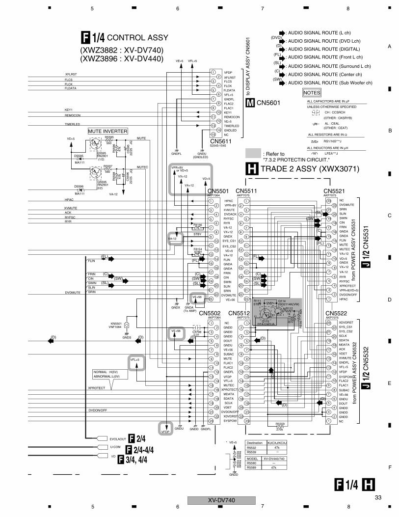
C
D
F
A
B
E
33
5 6 7 8
R5559
KN5501
C5798
CN5502 CN5512
R111
F8154
R11
3
R11
4Q115
R112
Q114
CN5522
D5596
R55
98
C55
96
F8156
CN5501 CN5511
R5597
D5595Q5595 C
5595
R55
96
R5595
CN5611
CN5521
I/O
EVOLAOUT
U-COM
SLINSRIN
FRIN
FLIN
SWINCIN
HPAC
DVDON/OFF
SYSPOW
XDVDRST
VDET
DVDON/OFF
SCLK
SDATA
NC
GNDD
GNDU
VE+56
from
PO
WE
R A
SS
Y C
N55
32
DOUT
GNDD
GNDD
XPROTECT
NORMAL :H(5V)ABNORMAL:L(0V) VFDP
VFL+5
MUTEC
XPROTECT
MDATA
MUTE
FLAC1
FLAC2
GNDFL
DOUT
GNDU
SUBAC
VE+56
GNDD
GNDD
GNDD
NC
DVDMUTE
(To AMP)
VE+56
DVDMUTE
SRIN
SLIN
SWIN
GNDA
FRIN
CIN
GNDA
FLIN
VD+5
VA+12
SUBAC
FLAC2SYSPOW
FLAC1
VFDP
GNDFL
VFL+5
XVMUTE
VDET
ACK
SDATA
MDATA
SYS_CS2
SCLK
SYS_CS1
XDVDRST
HPAC
XPROTECT
DVDON/OFF
VPR+8(VD+5)
from
PO
WE
R A
SS
Y C
N55
31
RYR
RYFSC
VX+12
VA-12
GNDX
MUTEC
VA+12
VD+5
RYR
ACK
RYFSC
(2/2)
Q5595
XVMUTE
VX+12
GNDX
SYS_CS1
SYS_CS2
RYFSC
RYR
VA-12
DVDACK
HPAC
XVMUTE
VPR+8V
(1/2)
MUTEC
MUTE INVERTER
KEY1
REMOCON
TIMERLED
MUTE
or VD+5
(GNDLED)
VE+5
TIMERLED
GNDLED
NC
FLAC2
FLAC1
KEY1
REMOCON
to D
ISP
LAY
AS
SY
CN
5601
MUTE
FLIN
GNDA
GNDA
CIN
FRIN
SWIN
SLIN
SRIN
DVDMUTE
NC
FLCS
XFLRST
FLDATA
GNDD
FLCK
R5532
R5590
R5539
R5589
VE+5*
VFL+5
GNDFL
FLCK
FLDATA
VFDP
FLCSXFLRST
22
23
22
23
21
18
17
2019
21
18
17
2019
21
56
4
3
13
16
15
14
13
14
16
15
1112
9
10
1211
9
10
6
78
5
87
56
3
12
4 4
3
21
C
22
21
23
20
22
21
23
20
16
18
17
19
16
18
17
19
15
12
13
14
15
12
13
14
11
78
9
10
15
14
12
13
16
18
17
19
22
21
23
20
E
B
E
C
B
4
2
3
1
56
78
10
9
1112
11
8
9
10
11
9
8
10
56
7
4
56
7
4
3
21
3
21
13
12
14
15
9
11
8
10
13
16
15
14
18
17
1920
22
21
23
6
4
7
5
3
12
VFDPGNDU GNDD GNDFL 270k
VFL+5
VNF1084
GNDS
VE+560.01
DTA124EUA
GNDX GNDA
VE+56
AKP7064 AKP7075
STBY
STBY
220k
2SD2114K(VW)82
k
1kAKP7075
RN2901
MA111 VA-12
47k
22/2
5
VA-12
STBY
AKP7064
VX+12
VA+12
VD+5
AKP7075
MA111
RN2901
560 JQ22
/25
47k
JQ560
VD+5
VPR+8V
GNDUGNDFL
52045-1545
AKP7075
VE+5 VFL+5
ALL INDUCTORS ARE IN µH
RS1/16S***J
LFEA***J
ALL RESISTORS ARE IN Ω
(OTHER : CEAT)AL : CEAL
CH : CCSRCH
ALL CAPACITORS ARE IN µF
UNLESS OTHERWISE SPECIFIED
NOTES
(OTHER : CKSRYB)
(D)
(D)
(D)(D)(D)(D)
(D)
(FL)
(SL)
(C)(SW)
(FL)(FL)
(FL)
(SL)
(C)(SW)
(SL)
(SL)
(C)
(C)
(SW)
(SW)
: AUDIO SIGNAL ROUTE (DIGITAL)(D)
: AUDIO SIGNAL ROUTE (L ch)
: AUDIO SIGNAL ROUTE (Front L ch)(FL)
: AUDIO SIGNAL ROUTE (Surround L ch)(SL)
: AUDIO SIGNAL ROUTE (Center ch)(C)
: AUDIO SIGNAL ROUTE (Sub Woofer ch)(SW)
: AUDIO SIGNAL ROUTE (DVD Lch)(DVD)
: Refer to "7.3.2 PROTECTIN CIRCUIT."
F 2/4
F 3/4, 4/4F 2/4-4/4
CN
5531
CN5601
J1/2
CN
5532
J1/2
M
TRADE 2 ASSY (XWX3071)H
F 1/4 H
F 1/4 CONTROL ASSY
(XWZ3882 : XV-DV740)(XWZ3896 : XV-DV440)
R5589 47k
MODEL
R5532R5539
R5590
Destination
XV-DV440/740
KUCXJ/KCXJ
47k
XV-DV7405 6 7 8
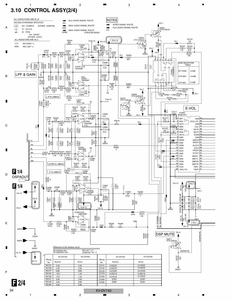
C
D
F
A
B
E
XV-DV74034
1 2 3 4
3.10 CONTROL ASSY(2/4)
C
SW4645
XD
SP
MU
TE
DS
PA
OU
T
SR
SL
FR
FL
-
+
-
+
-
+
+
-
+
-
+
-
R37
07
C3086 R3084
R30
86
R3300
C30
88
IC3053
R30
83
C30
41
C30
87
R30
93
R3087 R3089
C3085
R30
35
R3085
C3175
R3091
C3078
C3074
R3076
C3090
C3094
R3090 R3096
R30
88
C30
97
R30
92
R31
88
R30
97
R30
98
Q3071
R3101
R31
18
D30
52D
3053
C31
14
C31
16
C31
13
C31
15
IC3053
C3092
R3099C3093
C30
91
C3089
R3195
C3080
R3194
R31
19
C31
73
C3070
C30
72
R3072R3070
R30
68
R3074
R31
92
C30
76
C3069
C30
71
R30
67
R3071
C30
75
R31
91
R3069
C3073
R3073
C3052
C30
44
R31
34
R3075
R3052
R3056
R3058
C3077
R31
36
R31
33
R31
35
C30
43
R3054
C30
54
R31
90
C30
58C
3056
C30
53
C30
55
IC3052
R30
77R
3078
R3080
C3084
IC3052
C3079C3083
R3079
C31
74
R3132
R3131
C3118
IC3062C3117
R3193
C3060 Q3069
Q3070
IC3051
C3066
R30
62
C3062 R3064
R31
21
R3196
R3124
R3126
C31
01
R3128C3102
IC30
59
C3051R
3189
IC3051C
3057
R3051 R3053R3057
R3055
C3067
C3068
R30
59
R30
60
C3065
R30
61
C3061
R3063
C3059
Q3060
R31
20
R3197
R3127
R3125
Q3061
R3123
BC
E
2
3
2
81
4
45
86
7
81
20 21
17
15
18
16
19
26
25
23
24
22
3
5
6
3
2
4
87
4
14
13
11
12
28
27
30
29
7
9
10
8
34
31
33
32
3
4
5
6 35
36
38
37
1
2
40
39
B
C
E
B
81
4
C
E
1 43 7652
5
6
4
87
B
14 8910111213
E
C
BC
E
GNDD
VA-12
GNDD
22k
GNDA
3.3k
10/50 2.2k
3.3k
GNDA
ST
BY
47k
47p
1500
p
5.6kVD+5
VA+12
10/50
1.5k
1.0k
ST
BY
2.7k
10
5.6k
CH820p
CH
1.0k 1.5k
STBY
2.7k
5.6k
6800p10/50
1.2k 0
BA4558F
100k
1500
p
VUA-12 VA-12
ST
BY
47K
ST
BY
DTA124EUA
VD+5
VA-12
VA-7
GNDA
1.8k
1/2W
VM
150
UD
ZS
6.8B
220/
10
UD
ZS
6.8B
0.01
0.01
BA4558F
22
5.6k
0.01
10/50
0.01
820p
10/50
5.6k
0
1/2W
VM
220/
10
150
VA+12 VA+7
10/5
010/16
1500
p
JQ
5.6k47
k
10/16
47k
1500
p
JQ1.5k
5.6k
1.0k
ST
BY2.7k
ST
BY
10/16
0
5.6k
820p
27k12k 2.2k
39k
ST
BY
ST
BY
ST
BY
GNDA
330p
JQ
ST
BY
ST
BY
820p
BA4558FC
H
1500
p
BA4558F
GNDA
47K
47K
0
1500
p
BA4558F
0.01
10/500.01
0
GNDD VA-7
10/5
0
10k
10k
STBY
BD3814FVSTBY
CH
5.6k
CH68p
DTA124EUA
DTC124EUA
BA4558FJQ
0.01
47/16
10/16JQ
ST
BY
820
10k
1.2k
15k
10k
8.2kVA-7
VA+7
0.01
0.01
TC
4066
BF
N
0
10/16S
TB
Y
330p
CH
820p
ST
BY12k 27kJQ
2.2k
39k
0.01
CH68p
22 ST
BY
47/16JQ
ST
BY
820
10/16JQ
VA+12VUA+12 DTC124EUA
VA+7
GNDDVA-7
1.2k
10k
8.2k
10k
DTA124EUA
15k
VA+7
DSPMUTE
(SW
)
C fc=48kHz
LS,RS fc=48kHz
(SW)
SW
(2/2)
+9.5dB
(SW)
DSP MUTE
SW
FM
IXD
TS
DM
IX
(SW
)
VA-7
+9.5dB
(1/2)
C
+9.5dB
VA+7
(FL)FLINVEE(-7V) TNFR
TNFLGNDFRINGNDCIN
(C)
BNF1RBNF2RBNF1LBNF2L
(SL)
(FL)
LPF & GAIN
* *
L,R fc=48kHz
*
* **
(2/2)SR
(1/2)
+9.5dB
(SL) (SL)
(SL)
SRINGNDSLINGND FLOUT
FROUTCOUT
SLOUT
(SW)
OUT2GNDSWINGND SROUT
GNDDGND
SWOUT
(FL)
OUT1GNDINP2INN2 MUTE
DATACLKGND
INP1INN1 VCC(+7V)
GND
SL
FR
VUA-12
+0.0dB
(2/2)
E-VOL
LFE MIX -2.5dB
BY PASS
DTS MIX +3.6dB
-4.0dB
ALL CAPACITORS ARE IN µF
UNLESS OTHERWISE SPECIFIED
ALL RESISTORS ARE IN Ω
RD1/2VM***J
RS1/16S***J
(FL)
AL : CEALHA : CEHAT
(OTHER : CEAT)
CH : CCSRCH
TY : CFTYA
(OTHER : CKSRYB)
(SWB): SWch AUDIO SIGNAL ROUTE
(SL)
: SWch AUDIO SIGNAL ROUTE
: SLch AUDIO SIGNAL ROUTE
(SW)
(1/2)
+0.0dB(FL) (FL)
FL
VUA+12
(THEATER BASS)(FL)
: FLch AUDIO SIGNAL ROUTE
: AUDIO SIGNAL ROUTE
NOTES
TABLEGAIN SELECTION
(FL)
VA-12
GNDA
GNDD
VD+5
VA+12
DSPAOUT
*1
R3157
R3184
R3158
R3156
R3155R3147R3108R3107
6.8k
5.6k5.6k
100k4.3k
470
470
4.3k
XV-DV740 XV-DV440
KUCXJ KCXJ
XV-DV740 XV-DV440
KUCXJ KCXJWiring
No.
3.6k3.6k
6.8k
5.6k100k1.2k
1.2k
5.6k
Difference of the Andrew circuit
All resistors are :All capacitors are :
Wiring
C3184C3185
C3183
C3179C3176
C3142C3141
No.
STBYSTBY
0.018/16
0.056/160.012/500.022/250.022/25
CKSRYB***K**-TRS1/16***J-T
STBYSTBY
-
0.012/50
0.018/25
0.056/16-0.018/25
0.018/25
F 1/4
F 1/4
F 2/4
1 2 3 4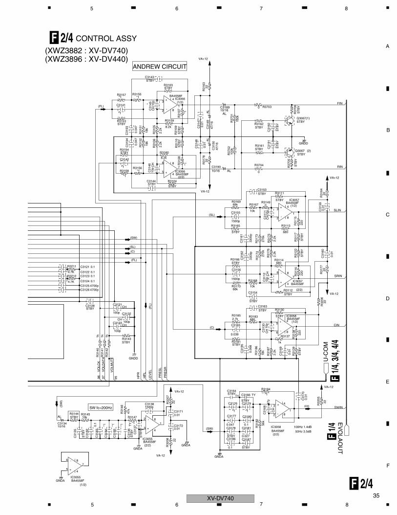
C
D
F
A
B
E
35
5 6 7 8
959796 HP
L
HP
R
LEV
EL
SWIN
CIN
SRIN
SLIN
RIN
FIN
+
-
+
-
+
-
+
-
+
-
+
-
-
+
+
-
IC3055
C31
82
C31
35
C3134
C31
83
C31
84
C31
85
IC3055
C31
37
C31
36
R3147
R32
08
C3172
C3186 C3187
C3177
C3178 C3181
C3180
R31
82
IC3058
R3144 R3145 R31
46
C3138
R31
40
R31
41
R31
42
R32
07
C3171
C3176 C3179
C3166C3164
C31
95
R3181
C3128
C3133
R3143
C3131
C3132
C3125C3126
R3211
R3212
C3124
C3121
C3123C3122
C3165
R3183R3185
R3170
C3154
R3168
C3156
C31
68
C31
70
R3184
R32
05
R31
87
R31
86
R31
39
C31
69
C31
30
R31
38
R3137
C3163R3130
IC3058
R32
06
R3112
C31
12
IC3057
R31
16
R31
77
C31
62
R3166
C31
61
C3155
R3165
R3167R3169
C3144
C3142
R3158R3156
R3154
R31
52
C31
94
R3153
C31
93
R31
51
R3104
C31
46
IC3056
R31
08
C3190
R31
78
R37
02
R31
06R3160
R31
10
C31
48
R31
05
R3159
C31
47
R31
09
C31
50
C31
49 R37
01
R31
74R3114
R31
76
R31
22
R31
73
R31
75
R31
17
C31
60
C31
11
R31
15
R3113
R3111
R3149IC3057
C31
59R
3164C3153
R3704 R37
05
C31
91
R3161
R3162
C31
92
Q3067
C3141
R3157 R3155
C3143
C31
45
R31
07
IC3056
R3103
C3189
R31
63
R3703
R37
06
5
6
4
87
3
2
4
81
3
2
1
4
8
5
6 87
4
5
6 87
4
54
6 87
2 81
34
3
2
4
81
GNDA BA4558F
0.1
ST
BY
10/16
AL 10kSTBY
*1 *1*1
BA4558F
GNDA
ST
BY
ST
BY
TY *1
VA-12 GNDA
22
GNDA
0.01
0.1
0.027
STBY
STBY
0.047 0.1 56k
BA4558F
CH
47k
1500p
GNDD
STBY
0.01
22
VA+12
STBY
*1*1
TYSTBYTY
0.06
8STBY
STBY
1k
100p
1k1k
CH
CH
100p
CH
100p
4700p4700p
0.1
4.7K
4.7K
0.10.1
0.1
0.039
6802.7k
68k10k
STBY
1500p
47p 0.
01
*1
22
VA+12
2.2k
18k
1k
0.01
ST
BY
10p
CH
220
STBY
STBYBA4558F
STBY
CH
10p
BA4558F
220
VA-12
2222
3300
p
STBY
STBY
3300
p
1500p
10k
VA-12
68k
*1
*1*1
STBY
18k
0.04
7
STBY
0.04
7
18k
STBYSTBY
BA4558F
CH
10p
8.2k
*1
22
10/16 AL
100k
2.2k
ST
BY
0.01
2.2k
8.2k
ST
BY
AL
47/1
6
0.01
47/1
6 100k
680
2.2k
270k
ST
BY
270k
2.2k
ST
BY
680
0.01
10p
CH
220
STBY
STBY
0BA4558F
0.01
22
0
ST
BY
STBY
VA+12
ST
BY
STBY
GNDD
STBY
ST
BY
STBY
*1
*1
*1
STBY
CH
10p
*1
STBY
BA4558F
AL10/16
AL
22
VA+12
0
ST
BY
(1/2)
(2/2)
(SW)
(2/2)50Hz 3.5dB
100Hz 1.4dB
(SW
)
SW fc=200Hz
VO
LMU
TE
VO
LCK
VO
LDA
TA
PR
ES
L
PR
ES
R
(FL)
(C)
(SW)
(1/2)
(2/2)
(C)
(FL)
(SW)
(SL)
(SL)
(2/2)
(1/2)
Q3067
(1)
(2)
(FL)
ANDREW CIRCUIT
* (1/2)
EV
OLA
OU
T
U-C
OM
F 2/4
F1/4
F1/4
, 3/4,
4/4
F 2/4 CONTROL ASSY
(XWZ3882 : XV-DV740)(XWZ3896 : XV-DV440)
XV-DV7405 6 7 8
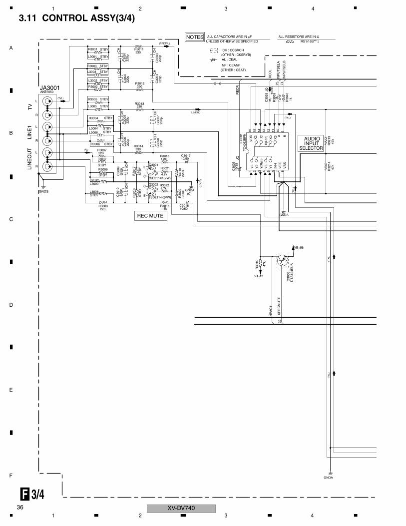
C
D
F
A
B
E
XV-DV74036
1 2 3 4
3.11 CONTROL ASSY(3/4)
F 3/4
HP
AC
1
32
RE
CR
75 74
RE
CL
E
C
C
B
B
E
31 2 4 8765
16 1415 10 91213 11
GNDA
VA-12
DT
A12
4EU
A
STBY
220
820p
STBY
820p
STBY
STBY
220
STBY
CH
CH
STBYSTBY
STBY
2SD2114K(VW)ST
BY
1.8k
220k
GNDA
10/50
47k
VE+56
GNDA
2SD2114K(VW)
ST
BY
CH
4.7k
4.7k
CH
1.8k
220k
10/50
220p
330
CH
220p
220p
CH
220p
10/3
5JQ
47k
TC
4052
BF
N
47k
AKB7050
STBY
STBY
STBY
STBY
STBY
STBY CH
STBY
STBY
CH
330
330
220p
220p
220p
CH
220p
330 CH
JQ
10/3
5
1k 1k
R30
10
Q30
03
L3008
R3008
C30
10
L3009
C30
09
L3007
R3009
R3006
R3007
R3004
L3006L3004
C30
05
R30
18
R3016 C3018
R30
20
Q3002
R30
17
R3022
Q3001
R3015
R3021
R30
19
C3017
C30
06
R3014 C30
08C
3007
C30
36
R32
14
IC30
01
R32
13
JA3001
R3005
L3005
R3002
L3002
R3003
L3003
L3001
C30
01
R3001
R3013
R3012C30
02
C30
04C
3003
R3011
C30
35
R30
40
R30
39
(TX
L)
XR
EC
MU
TE
GNDS
L
RLIN
EO
UT
LIN
E1
R
L
R
(FL)
REC MUTE
(C)
(TX
L)
(TX
L)
(LO
UT
)
Y2
Y0
Y(R
ch)
VS
SV
EE
INH
Y3
Y1
X2
VD
D
X0
X(L
ch) A B
X3X1
(TXL)
SELECTOR
AUDIO INPUT
TV
L(TVL)
(LINE1L)
(PRETVL)
INP
UT
SE
LA
INP
UT
SE
LB
AL : CEAL
(OTHER : CEAT)
(OTHER : CKSRYB)
NP : CEANP
UNLESS OTHERWISE SPECIFIEDNOTES ALL CAPACITORS ARE IN µF
CH : CCSRCH
ALL RESISTORS ARE IN ΩRS1/16S***J
1 2 3 4
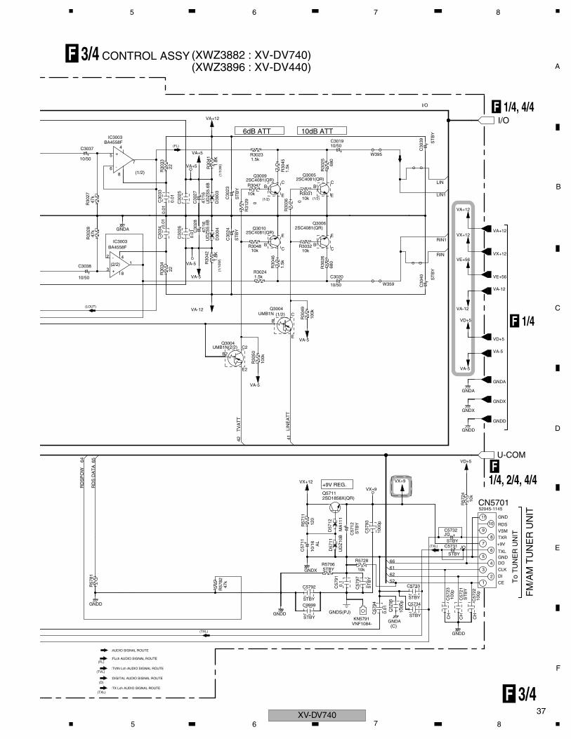
C
D
F
A
B
E
37
5 6 7 8
F 3/4
U-COM
GNDX
GNDD
GNDA
VA-5
VD+5
VA-12
VE+56
VX+12
VA+12
I/O
64 65
4142
6261
52
66
RIN
LIN
I/O
+
-
-
+
4
3
12
65
87
10
9
11
4
83
B2
C2
E2
B
E
C
2
1
6
7
8
BC
E
BC
E
E
BC
E
BC
4
5
GNDD
GNDDSTBY
VNF1084-
STBY
GNDA
1000
p
0.01
STBY
STBY
GNDD
CH
CH
CH
ST
BY
100p
100p
STBYGNDX 10k
0.1
ST
BY
AL
10/1
6
UD
Z10
B
120
MA
111
ST
BY
2SD1858X(QR)
VX+12
VA-5
JQ
STBY
STBY
1000
p
JQ
52045-1145
10k
VX+9
GNDD
VD+5
GNDX
GNDA
UMB1N
10/50
VA-12
22
VA-5
100k
VA-5
UMB1N
1.5k1.
5k
100k
10/50
BA4558F
47k GNDA
1.8K
0.01
0.01
47/1
6
47k
0.01
0.01
47/1
6
22
1.8K
10k
UD
ZS
5.6B
ST
BY 2SC4081(QR)
680
10k
2SC4081(QR)
10k
UD
ZS
5.6B
ST
BY
0
1.5k
2SC4081(QR)
1.5k
10k
0
2SC4081(QR)
680
VA-5
ST
BY
VA-12
VD+5
VE+56
VX+12
VA+12
BA4558F
10/50VA+5
VA+12
10/50
KN5791
C9999
C57
95
C57
94 C5734
C57
22
C57
21
C57
23
R5706
C5792 C57
91
C57
97
C57
11
D57
11
R5728
R57
11
D57
12
C57
12
C57
93
Q5711
C5733
C5731
C5732
CN5701R57
24
R30
34
R30
50
Q3004
Q3004
R3024R
3046
R30
49
R30
26
C3020
C3038
IC3003
R30
28
R30
42
C30
26
C30
34 C30
28
D30
04
R30
27
C30
25
C30
33
C30
27
D30
03
R30
33
R30
41
R3048
C30
24Q3010
R3032
Q3006
R3047
C30
23
R31
29
R30
36
Q3009
R30
45
R3031
Q3005
R30
25
C30
40
IC3003
C3037R3023
C3019
W395
W359
C30
39
:AUDIO SIGNAL ROUTE
(D)
(TVL)
(FL):FLch AUDIO SIGNAL ROUTE
:TVIN Lch AUDIO SIGNAL ROUTE
:DIGITAL AUDIO SIGNAL ROUTE
(TXL):TX Lch AUDIO SIGNAL ROUTE
(TXL)
GNDS(PJ)
(C)
RD
SP
OW
RD
S D
AT
A
+9V REG.VX+9
TV
AT
T
LIN
EA
TT
(TXL)
CE
DI
DO
CLK
TXR
+9V
GNDTXL
GND
RDS
VSM
(LOUT)
(2/2)
(1/2)
(1/1
0W)
(2/2) VA-5
(1/2)VA+5
(1/2)
(1/1
0W)
(1/2)
RIN1
LIN1
(FL)
6dB ATT 10dB ATT
To
TU
NE
R U
NIT
R57
81
47k
R57
82
ST
BY
FM
/AM
TU
NE
R U
NIT
F 1/4, 4/4
F 1/4
F1/4, 2/4, 4/4
F 3/4 CONTROL ASSY (XWZ3882 : XV-DV740)(XWZ3896 : XV-DV440)
XV-DV7405 6 7 8
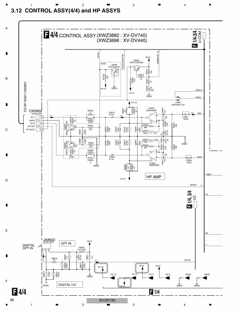
C
D
F
A
B
E
XV-DV74038
1 2 3 4
3.12 CONTROL ASSY(4/4) and HP ASSYS
+
-
-
+
OPTIN
7
26
27
2
RMC
HPR
HPL
LEV
ELS
HIF
T38
HPAC
HPAC1
LEV
EL 31
VA+12 VA-12 VD+5 VE+5 GNDDGNDA
I/O
U-C
OM
21 3
1
43
CB
E
3
5
2
4
1
E
CB
7
8 2
68
45
ST
BY
ST
BY
ST
BY
1k
0.1
47/1
6
VTF1096
GNDD
VA-12
ST
BY
VA+12
0.1
VD+5
GNDA GNDD
VE+5
TORX179PL
2SD
2114
K(V
W)
VD+5
VA-12
GNDD
0
STBY
47/16
47 47
NJM4565M47
pC
H
STBY
10
2SD
2114
K(V
W)
52045-0545
10
47k
ST
BY
100k
ST
BY
100k
10/5
0
ST
BY
ST
BY
39k
ST
BY
10/5
0
100p
100p
ST
BY
STBY
47k
047/16
39k47 NJM4565M47
47/1
62.
2k 39k
CH
CH
AL
AL
47/1
6
GNDA
39k
2.2k
CH
47p
STBY
GNDDVA-12
GNDD
VA+12
VA-12
47k
DTA124EUA
1k
47K
2SA1576A(QR)
DAP202K-TLB
10/1
6A
L15
k1k
VD+5
GNDS DIGITAL I-O
(D)
(D)
DIGITALOPT IN
OPT IN
STBY
HP AMP
HPDET
TO
HP
AS
SY
CN
3901
HP MUTE
HP DET
GNDA
HP R
HP L(FL) (FL)
(FL)
STBY XH
PM
UT
E
C86
13
C86
14
R86
11
C86
08
R8610 C86
09
C86
10
C86
11
JA8602
F8604
R3938
C3920
R39
28
R39
34
IC3901 C39
10 C3908
R39
40
Q39
08 C39
22
Q39
07
C39
21
CN3902
R39
39
R3936
R3942
R39
30R
3929
C39
18
C39
16
R3926C39
24
C39
17
C39
15
C39
23
C3913
C3914
R3941
R3935
R3937
C3919
R3925R
3927
R39
33
C39
12R
3924
R39
22
C39
11
R39
21
R39
23C
3909
IC3901
C3907
R31
48
Q3065
R3918
R39
00
Q3906
D3901
C39
06R
3917
R39
16
F1/4
-3/4
F1/4
, 3/4
F 1/4
F 4/4 CONTROL ASSY (XWZ3882 : XV-DV740)(XWZ3896 : XV-DV440)
F 4/4
1 2 3 4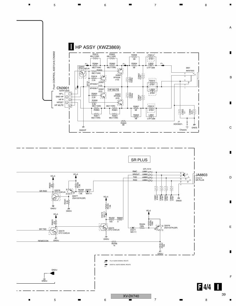
C
D
F
A
B
E
39
5 6 7 8
GNDU
B
E
C
C B
E
4
2
3
1
5
5
4
3
2
1
GNDU
1k 10k
GNDU
GNDU
DTC124EUA
47k
VE+5
GNDUGNDU
3.3k
GNDU
DTC124EUAMA111
100k2SA1037K(QR)
100k
MA
111
100 0
1.8k
ST
BY
VE+5
ST
BY
DTC124EUA
47k
VE+5
1.8k
2SA1037K(QR)
1.8k
MA111
VE+5
VE+5
QTL1013
GNDDST
BY
ST
BY
XKN3015
GNDHP
68(1/10W)
68(1/10W)
68(1/10W)
68
68(1/10W)
CTF139968
68 STBY
52044-0545
2.2k
2.2k
XP4506-T
XP4506-T
68(1/10W)
2.2k
DTA124EUA 68(1/10W)
XP4506
1000
p10
00p
0.04
7
STBY
STBY
XP4506
68(1/10W)
0.04
7
CTF139968
68 STBY
GNDS
0.1
0.01
AKN7003
68(1/10W) 68(1/10W)
REMOCON
SR TXD
SR RXD
TXDRXD
SR PLUS
SROUTRMC
34
2SR PLUS
6
Fro
m C
ON
TR
OL
AS
SY
(4/4
) C
N39
02
HP MUTE
HP L
HP RGND HP
HPDET
(FL)
(1/2)W13
1
(FL)
Q3901
(2/2)
(2/2)Q3921 HP MUTE
(1/2)
(FL) (FL)
Chassis
XDX3021-J1
4
1
3
2
5
R54
97
Q5579
R56
23
R54
91
R5496
Q5575D5571
R5494Q5576R
5495
D55
73
R5492 R8883
R54
93
C88
82
C88
81
Q5578
R56
22
R5498
Q5577
R54
99
D5570
L8883
L8884
L8881
L8882
C88
83
C88
84
JA8803
R3911
R3963
R3909
R3901
R3961
R3903
R3907
L3901
R3913
CN3901
R3906
R3920
R3905
R3919
Q3903
R3964
C39
02
Q3921 C39
01
C39
04
L3903
Q3901
R3962
C39
03
R3915
R3904 L3902
C39
25
C39
05
3901
R3912 R3902 R3908 R3914
I HP ASSY (XWZ3869)
F 4/4 I
(D)
(FL):FLch AUDIO SIGNAL ROUTE
:DIGITAL AUDIO SIGNAL ROUTE
XV-DV7405 6 7 8
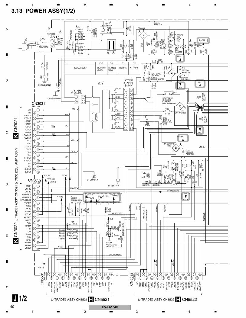
C
D
F
A
B
E
XV-DV74040
1 2 3 4
3.13 POWER ASSY(1/2)
J 1/2
UN+8V
SL
VL-
XPROTECT
HP
AC
RY
FR
YR
PO
WE
R
SU
BA
C
VL+
C
SR
VH+
FR
SW
FL
VH-
UN+8V
12104 62 8
1 3 5 7 9 11 13
2214 2016 18
12
3
4
515 17 19 2321
6 8
9
10
7 1112
13
14
15
16
21
22
2317
18 2019
20
22
21
23
16
18
17
19
12
14
15
13
8
10
9
11
6
4
5
7
21
3
23
20
22
19
21
21
C E
B
16
18
15
17
10
12
14
13
11
6
87
9
2
4
5
3
1
2
1
9
10
7
8
4
5
6
1
2
3
1 2
1 2
21
2
1
3 2
4
1
21
12
3
OUTIN
+-
+-
+-
+-~
~
OUTIN
~
~
~
~
~
~
CN
5531
CN
5532
R9505
R9503
R9504
R9501
C67C
66
IC61
CN3032
R13
2
R13
1
R133TH
131
D67
D10
3
Q13
1
D31
IC31
Q32
R37D32
R31
C32
D35
C34
C33
D34
D33
D36
R36 C
36
R35
C35 C37
CN3031
KN
1
CN2
C22
D22
C25
H3
H4
C24
CN11
C27
R21
C26
IC22D21
IC21
C23
IC12
D11 C15
C16
C1
H1AN1 H2
L1
T2
C57
C56
C51
C58 C
52
C2
RY1
D51
D52
IC11
R53
R54
D53
R51
IC51
C53
C54
Q51
R52
AK
P70
64
VA-12
AK
P70
64
VE
+56
VF
L+5
0
0
0
0
22/5
0
0.04
7
AKP7064 VPR+8
VP+15
NJM7812FA
VFL+5
VPR+8M
VD+5
GNDD
GNDX
2SC
4081
(QR
)
V+5
ST
BY
MA
111
VA+12
VM
+12
VX+12VF+12 VDVD+12
S5688G
GND ST
BY
S5688G
PM
F
2SB1565(EF)
VFDP
100
220/
63
MT
ZJ1
6B
(1/2
W)
1SS
133
MT
ZJ1
6B
3.3k JQ
JQ22
/50
MT
ZJ6
.8B
10022
/50
ST
BY
4.7k
JQ10
/50
ST
BY
AKP7064
VN
F10
84
B2P3-VH
4700p
MD5SBA20(B)
UN+8V
6800/25ACH7183
AK
R70
01A
KR
7001
D5SBA20(B)STBY
VL-
5600
/35
XC
H30
23
B10P-VH
M 4700
p
M
4700
p
STBY
5600
/35
XC
H30
23
STBYVH-
XCH3024
(1/2
W)
PM
F
10
D5S
BA
20(B
)
2200/63
VL+
2200/63XCH3024
AKR7001
0.02
2
AKR7001
AC
E70
22
XTF3004
0.04
7
0.04
7
ST
BY 0.04
7
DF06SA
0.02
2A
CE
7022
XSR3008
1SS
133
STBY
VH+
1818 DAN217
NJM78M56FA
0.01
10k
47/1
6
2SD1858X(QR)
1k VE+56
to TRADE2 ASSY CN5521
HP
AC
VA
-12
VD
+5
VP
R+
8/V
D+
5
GN
DX
VX
+12
MU
TE
MU
TE
C
RY
RR
YF
SC
XP
RO
TE
CT
DV
DO
N/O
FF
VA
+12
GN
DA
(To
AM
P)
GN
DA
(To
AM
P)
to TRADE2 ASSY CN5522
SR
INS
LIN
SW
INC
INF
RIN
FLI
N
NC
DV
DM
UT
E
DO
UT
(AC
3)G
ND
D
NC
GN
DD
GN
DD
DVDPOWER
SU
BA
CV
E+
56
GN
DU
FLA
C1
FLA
C2
VF
DP
XV
MU
TE
VD
ET
SY
SP
OW
GN
DF
LV
FL+
5
XD
VD
RS
T
DV
DA
CK
MD
AT
AS
DA
TA
SC
LKS
YS
_CS
2S
YS
_CS
1
SRIN
VPR+8VPR+8GNDA
SWINCIN
FRIN
SLIN
to T
RA
DE
1 A
SS
Y C
N30
21 &
CN
3022
(for
AM
P A
SS
Y)
MUTECMUTE
FLINGNDA
VA-12VP+15
VD+5
VFL+5
Guard GNDFor
GNDREGXPROTECT
TUNER
GNDREG
UN+8VGNDF
UN+8V
SLOUT
VL-SROUT
SLOUTVL-
(SL)
CKT for D11Thermal sensor
STBYALL
!!
Low
Abn
orm
alP
RO
TE
CT
GN
DD
VD
2 x VEF1040-
SP CHASSIS
COUTVL+
SROUTVL+
SWOUT
COUTVH+VH+
SWOUT
FLOUT
GNDP
GNDS
FLOUT
GNDPFROUTFROUT
VH-
(SW)
(FL)
VH-
CHASSISGND
FLAC
FLAC
AC5V
AC5V
FU
2
VH
VL
VL
GND
VH
T1
VFDP
*ATT7077
SCREW:BBZ30P080FTC
HEAT SINK:XNH3030
BBZ30P080FTCSCREW:XNH3030HEAT SINK:
NEUTRAL
W133
STBY
W134
LIVEFU1
*STBY
(AC
E70
29)
W129
W130
(AC
E70
29)
*
W125
* FU1 FU2 T1 T2
1000
/16
BAIDEN PROTECT
R55
R56
D55
Q52
2.2k
22k
UD
ZS
20B
2SC4081K
N2
R1
VN
F10
84R
CN
1080
CHASSISGND
KCXJ, KUCXJ REK1069 REK1069 ATT7079XTS3075
XKP3042
CN
3021
KC
N30
22K
CN5521H CN5522H
(6.3A) (6.3A)
1 2 3 4
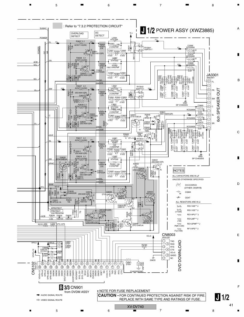
C
D
F
A
B
E
41
5 6 7 8
J 1/2
ACB
XPROTECT
VH+RYR
HPAC
SR
SL
RYF
VL-
C
VL+SW
VH-
AA
VH+
CC
FL
FR
PO
WE
R
ACB
POWER
SUBAC
30
29
28
27 23
24
25
26
17
18
1920
21
22
13
14
15
16
1112
56
78
910
12
3
4
56
7
E
BC
E
E
B
CB
B2
CE2
B2
C2
C2
CB
E
BC
C
E
E
B
B
E
C
B
C
E
E2B
C
E
B
E
C
B
12
3
4
C
E
CB
E
CB
E
46 5
1 2 3
B
EB
CE C
B
B
E
C
E
BC
2
5 4
31
6
C
E
CB
E
1
46
2
5
3
CN
5102
C8883C8886
C8884
C9901
C8885
C8881
C8882
R3701 L3701
D3632R3635
Q3637
D3633 C36
31
C36
32
C36
33
R36
38
R3780
Q3638
Q3632
R36
39
Q3640Q3633
D36
37
D3631
R36
32
R36
31
R36
34R3633 D3634
D3635 Q3631
D36
36
D36
11
R36
14
D3612
Q3612
R36
12
R36
13
Q3632
Q3639 Q3633
C3462D3613 R3464 C3464
R3616R3462
R36
44
R3642
Q3636
Q3642
CN8003
Q3635
R36
11
Q3611
R3618
R3617
D36
22
D36
21
R36
22
R36
23
R36
24
D3623
Q3622
C3461
L3462
R3463 C3463
R3615R3461
L3461
D36
43
RY3643 Q36
44
R36
30
R3640
R3626C3661 R3663 C3663
R3641
R3645 R36
43
Q3645
D3644
R3646
R3628
C3627
R36
21
Q3621
D36
01
D36
02
R3627
R36
04
R36
02
R36
03
Q3602
R3661
L3661
C3561
R3561R3625
R3563 C3563 D36
42
L3561
C3362D3603
C3364R3364
RY3642
R35
65
C34
68
C34
67
R34
68R34
66C
3466
R34
65 R34
67
C34
65
C36
67
R36
67
R36
65C
3665
R36
47
Q3641
C3470
C3469
C33
66
C35
67C
3565
C33
68
C33
65C
3367
C3669
R35
66
R33
66
R33
65R33
68
R33
67
JA3301
R3608
R36
01
Q3601
R3607
R3606
L3362
R3362
R3605
C3361
R3361
C3363R3363 D36
41 RY3641
L3361
C3569
C3370
C3369
VK
N12
61V
DV
D+
12
STBY
STBY
STBY
STBY
VN
F10
84
GNDD
VPR+8
1000/16
VPR+8 STBY
STBY
220
3.3k
VTL1075
1SS133 1SS133
2.2/
100
2SC4081(QC)
470/
6.3
10/5
0
0
VD+5
10k
2SC4081(QR)
UMB1N
DTC124EUARN1901
27k
MA
111
33k
33k
MTZJ5.1A
VD+5
DAN202K
4.7k10k 1SS133
2SC4081(QR)
MA
111
DTA124EUA
MA
111
33k
MA111
2SC4081(QR)
1.8k
ACN7112(2W)
33k
DTA124EUA
UMB1N
RN1901
0.022
DAP202K
4.7 0.022
27k (1/2W)PMF100
ATH-059
DTC124EUA
100k
1k
2SC4081(QR)
VKN1267
2SC4081(QR)1.8k
0.1
ACN7112(2W)0.1
MA
111
MA
111
2SC4081(QR)
1.8k
33k
33k DAP202K
0.022
(1/2W)PMF27k
4.7 0.022
100
ATH-059
0
MA
111
VF+12
ASR7017 2SC
4081
(QR
)
0
27k
0.022
(1/2W)PMF
4.7 0.022
10k
DAN217
100k
DTA143EUA 1k
27
ACN7112(2W)
STBY0.1
2SC4081(QR)
1.8k
MA
111
ACN7112(2W)
MA
111
0.1
33k
1.8k
33k
2SC4081(QR)
0.022 4.7
100
0.022
ATH-059
(1/2W)PMF27k
ATH-059100
MA
111
ASR7017
0.022 4.7 0.022
27k
DAP202K
(1/2W)PMF100
0.04
7
0.04
7
22 22 22
0.04
722
0.04
7
22
0.04
7
GND
0.04
7
XCG3008
2SD1858X(QR)
27
XCG3008
22
0.01
0.01
0.01
GND
XCG3008
0.04
70.
047
0.04
70.
047
0.04
70.
047
2222 22 2222 22
0.01
XKE3021
ACN7112(2W)0.1
1.8k
ACN7112(2W)
2SC4081(QR)
0.1
0.022 4.7
ATH-059
0.022
27k(1/2W)PMF
100
MA
111
ASR7017
ATH-059
VL+
XCG3008
XCG3008
XCG3008
0.01
0.01
from DVDM ASSY
:VIDEO SIGNAL ROUTE
:AUDIO SIGNAL ROUTE
VP
R+
8V
PR
+8
VP
R+
8(M
)
VD
VD
+12
VP
R+
8(M
)
GN
DM
GN
DM
GN
DD
GN
DD
XD
VD
RS
T
SY
S_C
S2
SY
S_C
S1
SC
LKS
DA
TA
MD
AT
A
GN
DD
DV
DA
CK
DO
UT
(AC
3)
GN
DD
DV
DP
OW
ER
XCH3021
DV
DM
UT
E
GN
DD
VD
ET
GN
DD
XV
MU
TE
CT
SR
TS
RX
DT
XD
NC CHASSISGND
KN
1
GNDDVD+5
DV
D D
OW
NLO
AD
NC
Low AbnormalPROTECT
TS
GNDSRGNDSL
TXDRXD
CTSRTS
PMF(1/2W)
FU(1/4W)RF1/4PS***J
RD1/2PMF***J(1W)
RD1/4PU***J
RS1LMF***J
(1/10W)RS1/10S***J
RS1/16S***J
CQMA
ALL RESISTORS ARE IN Ω
M
CEAT
UNLESS OTHERWISE SPECIFIED
(OTHER: CKSRYB)CH:CCSRCH
ALL CAPACITORS ARE IN µF
NOTES
SP CHASSIS
(SL) (SL) (SL)
GNDSWGNDC
(SW) (SW)
GNDFLGNDFR
(SW)
(1/1
0W)
(1/1
0W)
(1/1
0W)
(1/1
0W)
(1/1
0W)
(1/1
0W)
(SL)
SR
6ch
SP
EA
KE
R O
UT
SL
SP CHASSISC
SW
FR
(1/1
0W)
(1/1
0W)
(1/1
0W)
(1/1
0W)
(1/1
0W)
(1/1
0W)
FL
(FL)
OVERLOADDETECT
(FL)
DC DETECT
(FL)
(SW)
(FL)
: Refer to "7.3.2 PROTECTION CIRCUIT"
J 1/2 POWER ASSY (XWZ3885)
CN901B 3/3• NOTE FOR FUSE REPLACEMENT
FOR CONTINUED PROTECTION AGAINST RISK OF FIRE.REPLACE WITH SAME TYPE AND RATINGS OF FUSE.
CAUTION -
XV-DV7405 6 7 8
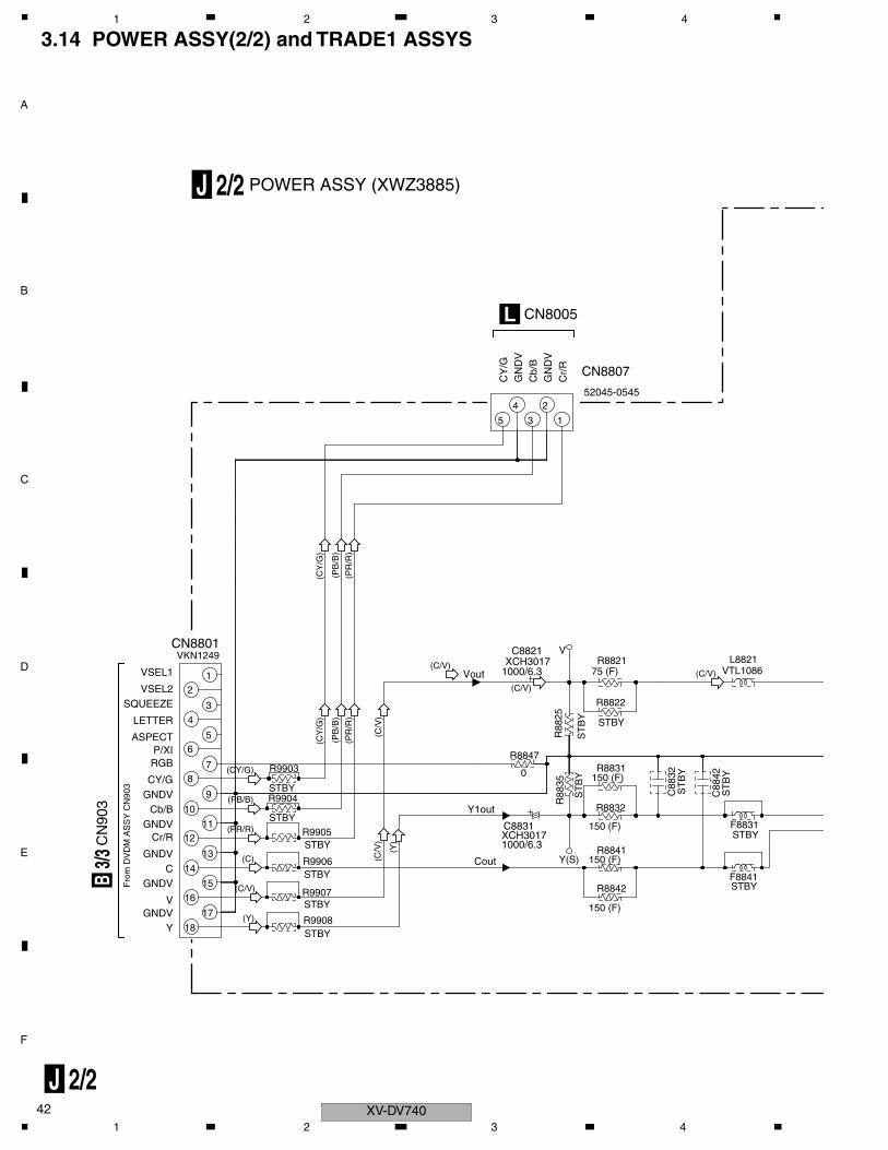
C
D
F
A
B
E
XV-DV74042
1 2 3 4
3.14 POWER ASSY(2/2) and TRADE1 ASSYS
J 2/2
R9908
R9907
R9904
R9906
R9905
R9903
CN8801
R88
25
R8822
C8821R8821 L8821
STBY
STBY
STBY
STBY
STBY
STBY
VKN1249
ST
BY
STBY
XCH30171000/6.3 75 (F) VTL1086
Fro
m D
VD
M A
SS
Y C
N90
3
GNDV
GNDVY
GNDV
V
Cr/R
GNDVC
Cb/BGNDV
ASPECT
SQUEEZE
LETTER
VSEL1
VSEL2
CY/G
P/XIRGB
Vout
V
17
18
15
16
13
12
14
11
10
9
6
78
5
3
4
21
CN8807
CY
/G
Cr/
RG
ND
V
GN
DV
Cb/
B
R8847
0
R8842
C8831
R8841
R88
35
R8832
F8841
C88
32
F8831
C88
42
150 (F)
1000/6.3XCH3017
150 (F)
ST
BY
150 (F)
STBY
STBY
ST
BY
Cout
Y1out
Y(S)
R8831
ST
BY
150 (F)
CN8005L
52045-05454
5
2
13
(Y)
(Y)
(C)
(C/V)
(C/V)
(C/V)
(C/V)
(C/V
)(C
/V)
(CY/G)
(PR/R)
(PB/B)
(CY
/G)
(PR
/R)
(PB
/B)
(CY
/G)
(PR
/R)
(PB
/B)
CN
903
B3/3
J 2/2 POWER ASSY (XWZ3885)
1 2 3 4
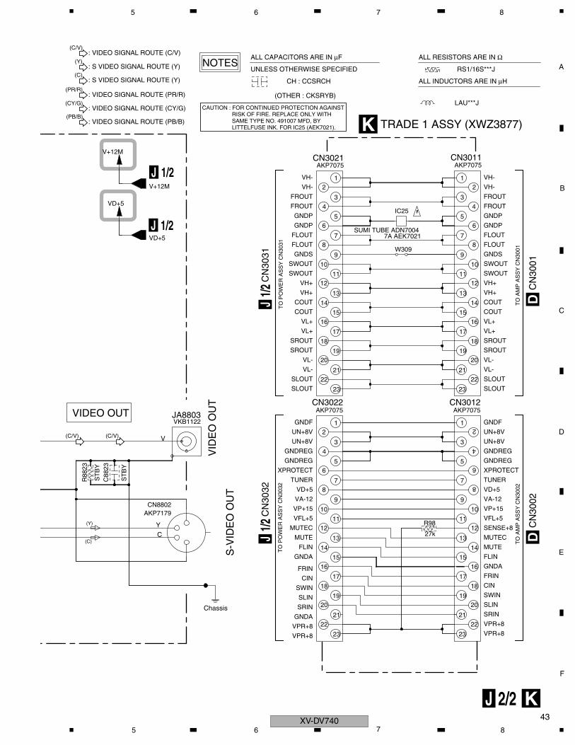
C
D
F
A
B
E
43
5 6 7 8
J 2/2 K
V+12M
VD+5
V
CN3022
R98
CN3012
R88
23
C88
23
JA8803
W309
IC25
CN3021 CN3011
AKP7075
27k
AKP7075
ST
BY
ST
BY
VKB1122
7A AEK7021SUMI TUBE ADN7004
AKP7075 AKP7075
VD+5
V+12M
SLIN
SRIN
GNDA
VPR+8
VPR+8
TO
PO
WE
R A
SS
Y C
N30
32
VPR+8
SRIN
VPR+8
SLIN
SWIN
CIN
FRIN
SWIN
GNDA
FLIN
MUTE
MUTEC
VP+15
VFL+5
VD+5
VA-12
TUNER
GNDREG
XPROTECT
UN+8V
UN+8V
GNDREG
SLOUT
SLOUT
GNDF
GNDA
FRIN
CIN
FLIN
MUTE
TO
AM
P A
SS
Y C
N30
02
SENSE+8
VFL+5
MUTEC
VP+15
VA-12
VD+5
GNDREG
TUNER
XPROTECT
GNDREG
UN+8V
UN+8V
GNDF
SLOUT
SLOUT
VIDEO OUT
Chassis
VID
EO
OU
T
VL+
VL+
SROUT
SROUT
TO
PO
WE
R A
SS
Y C
N30
31
VL-
VL-
COUT
SWOUT
VH+
VH+
SWOUT
COUT
GNDS
GNDP
FLOUT
GNDP
FLOUT
FROUT
VH-
VH-
FROUT
VL-
SROUT
VL-
VL+
VL+
SROUT
TO
AM
P A
SS
Y C
N30
01
COUT
COUT
VH+
SWOUT
VH+
SWOUT
GNDS
FLOUT
FLOUT
GNDP
GNDP
FROUT
FROUT
VH-
VH-
(OTHER : CKSRYB)
CH : CCSRCH
ALL CAPACITORS ARE IN µF
UNLESS OTHERWISE SPECIFIEDNOTES
LAU***J
ALL INDUCTORS ARE IN µH
RS1/16S***J
ALL RESISTORS ARE IN Ω
1920
21
22
23
2019
21
22
23
14
16
18
15
17
9
10
1112
13
8
4
5
7
2
3
6
22
23
1
14
16
17
18
15
12
13
11
8
9
10
5
6
7
2
3
4
1
22
23
20
18
19
21
16
17
12
10
11
13
14
15
4
56
78
9
2
3
1
1920
21
16
17
18
13
15
14
10
1112
87
9
4
56
12
3
YC
CN8802AKP7179
S-V
IDE
O O
UT
(C)
(Y)
CAUTION : FOR CONTINUED PROTECTION AGAINST RISK OF FIRE. REPLACE ONLY WITH SAME TYPE NO. 491007 MFD, BY LITTELFUSE INK. FOR IC25 (AEK7021).
: S VIDEO SIGNAL ROUTE (Y)(Y)
: S VIDEO SIGNAL ROUTE (Y)(C)
: VIDEO SIGNAL ROUTE (C/V)(C/V)
: VIDEO SIGNAL ROUTE (CY/G)(CY/G)
: VIDEO SIGNAL ROUTE (PR/R)(PR/R)
: VIDEO SIGNAL ROUTE (PB/B)(PB/B)
(C/V) (C/V)
J 1/2
J 1/2
CN
3031
J1/2
CN
3032
J1/2
CN
3001
DC
N30
02D
TRADE 1 ASSY (XWZ3877)K
XV-DV7405 6 7 8
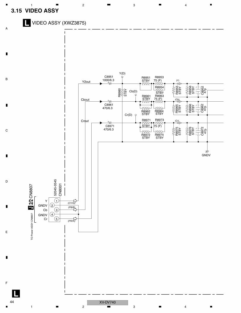
C
D
F
A
B
E
XV-DV74044
1 2 3 4
3.15 VIDEO ASSY
L
CN
8001
TO
Pow
er A
SS
Y C
N88
07 GNDV
GNDVCb
Cr
Y
R8972 R8974 R89
75
C89
72
R89
76
C8961
C8971
R8971
R8962
C8951
R89
80
R8961
R8951
R8973
R8964 R89
65
C89
62
R89
66
R8963
R89
55
R8953
R8954
C89
52
R89
56
Crout
Cr(D)
Y2out
Cbout
Cb(D)
(Cr)
(Cb)
(Y)
Y(D)
470/6.3
STBY
GNDV
STBY
ST
BY
47p
ST
BY
470/6.3
STBY
STBY
1000/6.3
ST
BY
STBY
STBY
75 (F)
STBY
ST
BY
ST
BY
47p
75 (F)
STBY ST
BY
75 (F)
47p
ST
BY
4
2
5
3
1
5204
5-05
45
(CY/G)
(PR/R)
(PB/B)
CN
8807
J2/2
VIDEO ASSY (XWZ3875)L
1 2 3 4
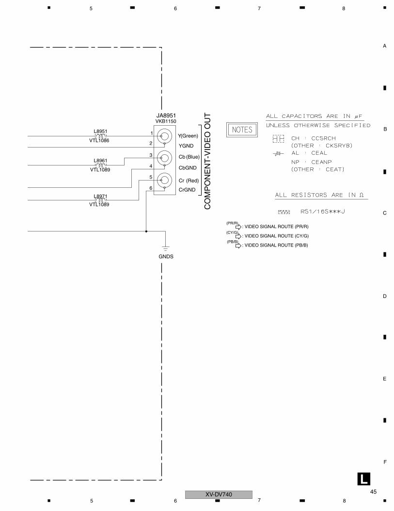
C
D
F
A
B
E
45
5 6 7 8
L
L8971
L8961
L8951
JA8951
5
4
6
3
2
1
GNDS
(Red)Cr
CbGND
CrGND
(Blue)
YGND
Cb
Y(Green)
VTL1089
VTL1089
VTL1086
VKB1150
CO
MP
ON
EN
T-V
IDE
O O
UT
: VIDEO SIGNAL ROUTE (CY/G)(CY/G)
: VIDEO SIGNAL ROUTE (PR/R)(PR/R)
: VIDEO SIGNAL ROUTE (PB/B)(PB/B)
XV-DV7405 6 7 8
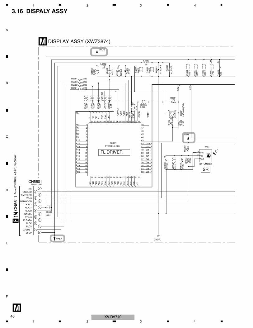
C
D
F
A
B
E
XV-DV74046
1 2 3 4
3.16 DISPALY ASSY
M
Vcc
Vout
GND
P24
P21
P22
P23
P26
P28
P25
P30
P27
P29
P32
P31
P35
P34
G1
P33
P20P19
P15
P18
P16P17
P14
P12P11
P13
P10
P8P9
P7
P5
FL
P6
G3G2
G5G6
G4
G7
G10
G8
G11
G9
P4
P2
P3
P1
P37
LED
P36
LED
G12
C5681
CN5601
R5663
R5662
R5664
R5661
IC5601
C59
52
C59
53
R59
52
R59
51R
5953 5951
C56
73
C56
72
C56
71
C56
77
C56
76
R56
74
C56
74 C5675
R56
93
R56
95Q
5691
R5691
C55
62
L5562
C55
64
C55
63
C56
65
D55
61
C56
66
L5563
D56
62
C56
78
C56
68
C56
62
C56
67
C56
61
C56
79
VFDP
0.01
52044-1545
GNDFL
PT6302LQ-003
47/1
6
0.02
2
ST
BY
AL
ST
BY
GP1UM27XK
47
VE+5
1000
P
1000
P
1000
P
0.01
3.3K
47P
CH
0.022
VC
X10
01
220
220
220
220
1k
ST
BY
2SC
4081
(QR
)
47k
0.02
2
22 AL
0.02
2
100/
6.3
ST
BY
0.02
2
0.02
2
10
VFL+5
MT
ZJ3
6B
22/3
5A
L
ST
BY
ST
BY
ST
BY
470p
1/50
CH
AL
VFDP
Fro
m C
ON
TR
OL
AS
SY
(1/4
) C
N56
11
FLDATAFLCKFLCS
XFLRST
VFL+5GNDFLFLAC2FLAC1
TIMERLED
KEY1REMOCON
VE+5
GNDLEDNC
FL DRIVER
SR
FLD
AT
A
FLC
K
FLC
S
RS
T
GN
DD
VF
DP
15
1112
13
14
87
9
10
3
4
56
12
191817
16
15
2120 2523 2422
14
13
12
11
292826 27 3130 32
33
34
38
37
35
36
8
7
10
4
3
6
5
9 40
41
42
39
43
44
46
45
2
1
3
6263
1
2
64 61 60 57 565859 50535455 52 51
47
48
49
BC E
CN
5611
F1/4
DISPLAY ASSY (XWZ3874)M
1 2 3 4
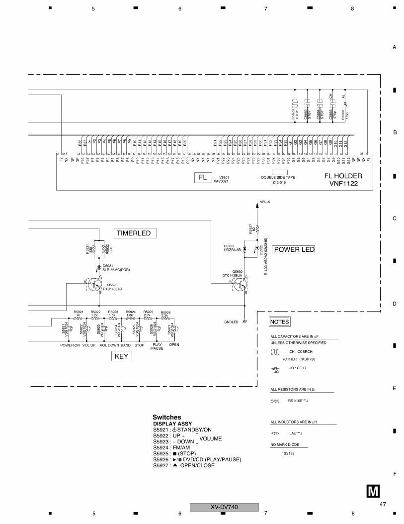
C
D
F
A
B
E
47
5 6 7 8
M
P37
P36 P
1P
2
P14
P12
P13
P10
P11P
3P
4
P6
P5
P7
P8
P9
P20
P17
P18
P16
P15
P19
P21
P22
P23
P24
P25
P26
P29
P27
P28
P30
P31
P32
P35
P33 G1
G3
G2
P34 G9
G4
G8
G7
G5
G6
G11
G10
G12
S59
21
S59
23
S59
22
S59
24
S59
25
S59
26
R5922R5921 R5923 R5924 R5925
S59
27
R5926
R59
31
D5931
Q5693
R59
32
Q5692
D5933
D59
32
R59
27
V5601
C56
70
C56
63
C56
64
C56
69
C56
80
VS
G10
24
VS
G10
24
VS
G10
24
VS
G10
24
VS
G10
24
VS
G10
24
1.2k1k 1.5k 1.8k 2.7k
DTC143EUA
VS
G10
24
3.3k
GNDLED
330
SLR-56MC(PQR)
330
DTC143EUA
UDZS6.8B82
VFL+5
ST
BY
ST
BY
ST
BY
CH
1/50
470p
AL
VOL UPPOWER ON
KEY
BANDVOL DOWN STOP/PAUSE
PLAY OPEN
TIMERLED
E1L
33-A
B0A
2-02
(234
5)
P36
P37F
2
P11
P10
P13
P12NX P2
NP
NP P1
P8
P7
P3
P4
P5
P6
P9
P18
P17
P19
P20
P14
P15
P16
FLXAV3021
P24
P21
P32
DOUBLE SIDE TAPE
P28
P27
P31
P30
P29
P23
P22
P26
P25NX
NX
NX
NX
NX
POWER LED
FL HOLDERZ12-016 VNF1122
P33
P35
P34
G12 F1
G11
G10G2
G1
G8
G3
G6
G4
G7
G5
NP
NP
G9
NX
E E
B
C
B
C
62 61 57 56 5558 52 51 50 4954 53 48 4447 46 45 43 40 39 3742 41 38 36 35 34 33 32 31 28 27 26 2530 29 22 2023 2124 141819 17 16 15 13 12 11 10 9 8 7 56 2 1
NO MARK DIODE
1SS133
LAU***J
ALL INDUCTORS ARE IN µH
RS1/16S***J
ALL RESISTORS ARE IN Ω
JQ : CEJQJQ
UNLESS OTHERWISE SPECIFIED
ALL CAPACITORS ARE IN µF
NOTES
(OTHER : CKSRYB)
CH : CCSRCH
DISPLAY ASSYS5921 : STANDBY/ONS5922 : UP +S5923 : – DOWNS5924 : FM/AMS5925 : 7 (STOP)S5926 : 6 DVD/CD (PLAY/PAUSE)S5927 : 0 OPEN/CLOSE
VOLUME
Switches
XV-DV7405 6 7 8
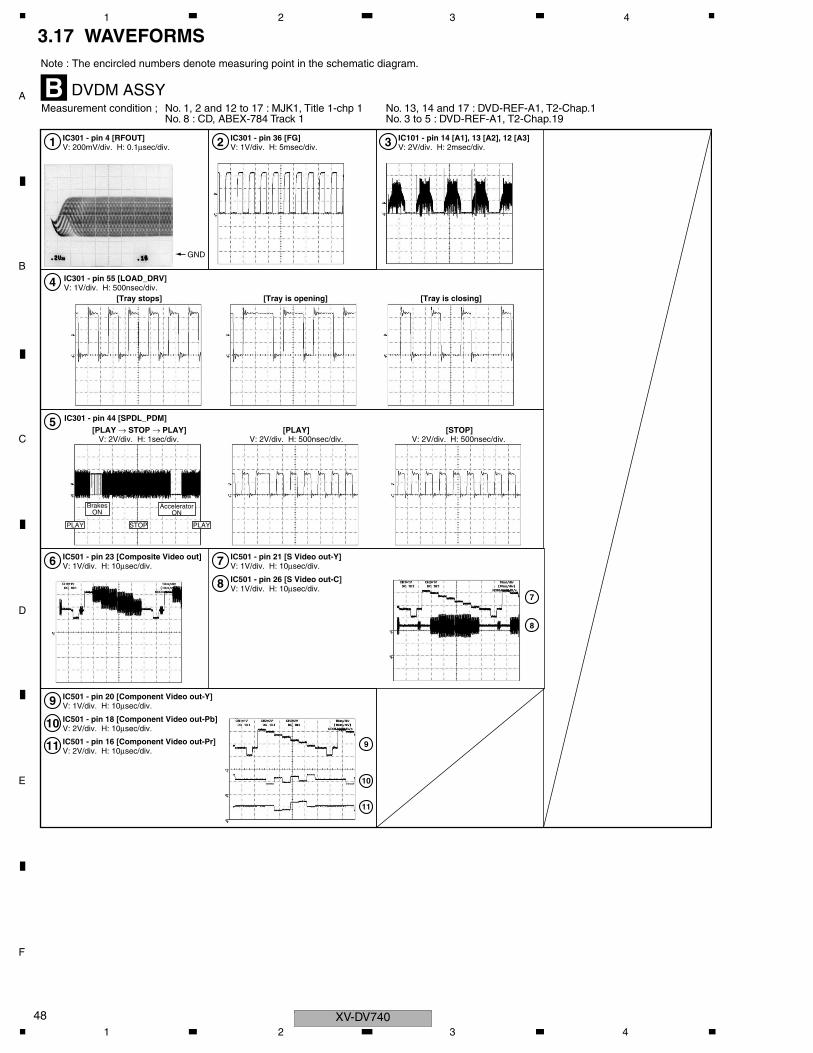
C
D
F
A
B
E
XV-DV74048
1 2 3 4
3.17 WAVEFORMS
1 IC301 - pin 4 [RFOUT]V: 200mV/div. H: 0.1µsec/div.
6 IC501 - pin 23 [Composite Video out]V: 1V/div. H: 10µsec/div. 7 IC501 - pin 21 [S Video out-Y]
V: 1V/div. H: 10µsec/div.
8 IC501 - pin 26 [S Video out-C]V: 1V/div. H: 10µsec/div.
9 IC501 - pin 20 [Component Video out-Y]V: 1V/div. H: 10µsec/div.
10 IC501 - pin 18 [Component Video out-Pb]V: 2V/div. H: 10µsec/div.
11 IC501 - pin 16 [Component Video out-Pr]V: 2V/div. H: 10µsec/div.
2 IC301 - pin 36 [FG]V: 1V/div. H: 5msec/div. 3 IC101 - pin 14 [A1], 13 [A2], 12 [A3]
V: 2V/div. H: 2msec/div.
4 IC301 - pin 55 [LOAD_DRV]V: 1V/div. H: 500nsec/div.
5 IC301 - pin 44 [SPDL_PDM]
DVDM ASSYBMeasurement condition ; No. 1, 2 and 12 to 17 : MJK1, Title 1-chp 1 No. 13, 14 and 17 : DVD-REF-A1, T2-Chap.1
No. 8 : CD, ABEX-784 Track 1 No. 3 to 5 : DVD-REF-A1, T2-Chap.19
Note : The encircled numbers denote measuring point in the schematic diagram.
GND
[Tray stops]
[PLAY → STOP → PLAY] [PLAY] [STOP]
[Tray is opening] [Tray is closing]
V: 2V/div. H: 1sec/div.
PLAY STOP PLAY
V: 2V/div. H: 500nsec/div. V: 2V/div. H: 500nsec/div.
BrakesON
AcceleratorON
7
8
9
10
11
1 2 3 4
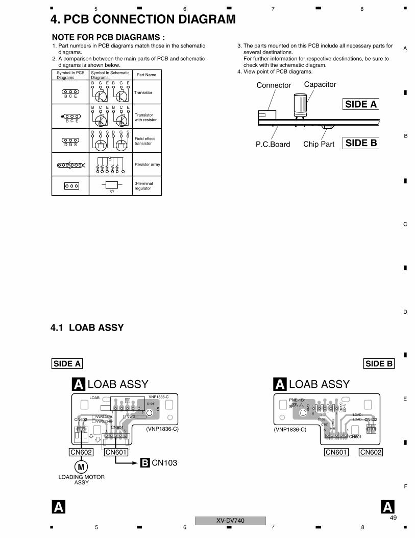
C
D
F
A
B
E
49
5 6 7 8
4. PCB CONNECTION DIAGRAM
4.1 LOAB ASSY
NOTE FOR PCB DIAGRAMS :1. Part numbers in PCB diagrams match those in the schematic diagrams.2. A comparison between the main parts of PCB and schematic diagrams is shown below.
3. The parts mounted on this PCB include all necessary parts for several destinations. For further information for respective destinations, be sure to check with the schematic diagram.4. View point of PCB diagrams.Symbol In PCB
DiagramsSymbol In SchematicDiagrams
Part Name
B C E
D
D
G
G
S
S
B C E
B C E
D G S
B C E B C E
B C E
Transistor
Transistorwith resistor
Field effecttransistor
Resistor array
3-terminalregulator
CapacitorConnector
P.C.Board Chip Part
SIDE A
SIDE B
15
5 1
SW
2
(V+
5D)
V+
3D
LOAD-
LOAD+
GN
D
PNE-1B1
C102
C101
CN602
CN601
1 2
51
VWG2346-VWG2279-
5
VWG
LOAB
51
VNP1836-C
CN602
S101
CN601
SIDE A SIDE B
LOAB ASSYA LOAB ASSYA
CN103B
(VNP1836-C) (VNP1836-C)
LOADING MOTORASSY
M
CN601CN602 CN601 CN602
A A
XV-DV7405 6 7 8
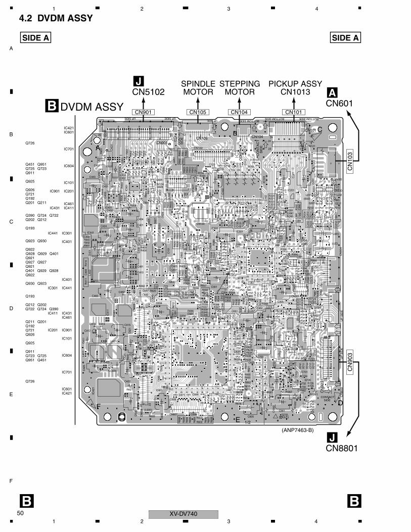
C
D
F
A
B
E
XV-DV74050
1 2 3 4
4.2 DVDM ASSY
E
C42
5
R354
112
14
58
26
50
51 757
6
210
17
1 2
1
53
10
51
56
208
24
145
8
18 9
16
291
14
130
111
11
11
18
18
134
5
51
14
51 75
1001
25
124
22 42
121
NP
19
24
23
2
1
1
8
104 53
52
1157
156
2 123
23242 1
1
5 4
2 30
7 1
857
1 4
130
11
8
5
C23
1
CN105
R12
3
R102
C10
2
C10
1
R20
4
C201
CN104
C120
C118C116
C12
6
C20
2
CN
103
R202
R20
3
IC201
C22
1
R20
1
R34
6
C346
R221
R223
C357
C33
5
Q20
2
R12
4
R222
R101
C362
R364
R361
R363
R36
5
R36
9
R368
C222
C12
4
L361
C34
2
C326C
323
C315
C30
9
C318
C34
8
C388
C377
IC301
C373
C391
C300
C132
C13
9
C14
2
C12
8C
127
CN101
C21
2Q
212
R21
4
C211
R21
3
R212
R21
1
IC10
1
C11
2
C11
3
C114
C13
0R
131
R13
5C
134
Q201
X30
1
CN301
R220
R36
6
R367C301
C302
C304
C305
R390Q390
L390
R39
2
R391
C39
3C
390
C392
C394
C303
Q211
C15
1
Q19
3
Q19
2
R15
1
L191
L192
L193
L194
C307
C306
C354
C13
3
R191
R19
2
R194
R196
R19
7
R199
R37
8
R37
9
R382R383
R38
5R
386
R384
R394
R396
R310R301
R334R333R332
R336R337
R33
8
R339R340
R341
R34
2
R34
4
R397R398
CN121CN122
CN123
CN124
R38
9
R30
0
IC601
C62
1
C64
4
C640
X601
C664
CN
609
CN
608
IC604
C69
0
C60
4C
614
C623
C630
C63
7C
648
C647
C681C694
C60
7
C619
C622
C63
6C
649
C641
C659
C671 C684
C698C66
0
C650
C651
C564
R1069R10
84
C561
C70
7
C70
6
C705
C70
8
R72
1
C70
9 R714
C71
0
C70
3
C70
2
R715R716
IC701R713R712
R71
1R724
Q722
Q72
1
R561
C73
1
R731
R73
3
C734
R726Q726
Q72
5
R725C73
2
R732R73
4
C733
R719R718
C71
7
R600
C60
0
R71
7
C652
Q72
3
C634
C605
R620
R64
0
R64
4
R60
9
R61
0
R61
2R
613
R626
R68
8
R68
9R
694
R69
5
R66
4
R602
R603
R60
6R
607
R60
8
R616
R617
R618
R619R611
R662
R663R665
R628 R635
R62
1R64
1
R634R636
R63
8
R637
R63
9R
651
R65
2
R65
7R
656
R65
5
R65
4R
653
R658
R67
5
R696
CN607
C642L641
R74
1R742
R74
4
R96
1
Q95
1
C15
63
C1562
R90
7R
906
IC90
1
R90
3
R90
5R
904
R90
2
R90
1
C902
Q91
1
R918
CN901
CN
902
IC42
1
IC41
1
IC441
IC431
D40
1
R41
0
R409
C410
C40
9
C491
C404
C403
C423
C424
C46
1
C415C414
C422
R45
1C
452
C401
D43
2
C431
C43
3
C432
C434
D43
1
C44
1
C442
C443
C451
CN
904
R96
0
R43
3
R44
4
R95
1
C413
C412
C462C463
R46
1
R462
R421
C41
1
C42
1
IC46
1
C92
1
R921
R40
1
R41
1
C901
C95
1
Q92
2
Q921
Q92
3
R92
2
D92
2R
926
R92
5R
923
R92
4
R93
4R
933
D92
7
D92
5
D92
3
Q925
R908
R90
9
Q926
R93
2
R93
1
R441
R443R442
D40
2R
402
C40
6
C40
7
R408
R40
7C
408
R403
R95
2R
953
R95
4R
955
R95
6R
957
R95
8R
959
R964R965
R96
6R
967
R96
8R
969
R1081
Q45
1
D92
6
C405
R10
82
R10
83
R962
R963
R40
0
R937R936
Q928
Q927
R938R939
R93
5
Q930
Q92
9
C10
3
CN
903
Q401
R11
1
CN921
CN
923
IC40
1
R562
C308
C12
1
C38
3
C382
C312C311
C31
0
R3
R4
R41
6
R647
R648
L402
R981
L421
D92
8
R723
R1
R722
Q724
R98
2
R98
4
R98
3
R2
L411
CO
NT
AC
TS
IDE
CO
NT
AC
TS
IDE
BOTTOM SIDEBOTTOM SIDE
BOTTOM SIDE
CO
NT
AC
T
UP SIDE
SID
E
UP SIDE
DF
A
B C
UP
SID
EU
P S
IDE
CONTACTSIDE
(650)
SID
EC
ON
TA
CT
D
1/2
(780)
30
UP SIDE
D
A
A
B
B
C
C
1
GNDD
V+5D
LD2LD1
RF
OU
T
(L600)
(L11
1)
DVDM ASSYB
(ANP7463-B)
PICKUP ASSYCN1013
STEPPINGMOTOR
SPINDLEMOTOR
B B
SIDE A SIDE A
CN8801J
CN
903
CN
103
CN101CN104CN105
CN5102J
CN601A
CN901
IC201
IC701
IC101
IC601
IC301
IC901
IC421
IC411
IC441
IC431
IC461
IC401
IC604
IC401
IC461
IC431
IC441
IC411
IC421
IC901
IC701
IC604
IC601
IC101
IC301
IC201
Q724
Q202
Q193
Q192Q201
Q723Q725
Q726
Q721
Q722
Q211
Q212
Q911
Q922
Q921
Q923
Q401
Q451
Q928
Q927
Q930
Q929
Q925
Q926
Q724 Q390
Q401 Q929
Q930
Q927
Q928
Q451
Q926
Q925
Q923
Q921
Q922
Q911
Q951
Q723 Q725
Q726
Q721
Q722
Q192
Q193
Q951
Q211
Q390
Q201
Q212Q202
1 2 3 4
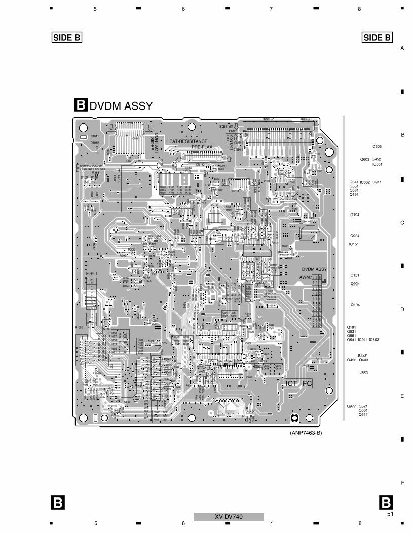
C
D
F
A
B
E
51
5 6 7 8
1
130
8 14
1
2 30
29
1 23
242
1
8
2527
30
7 1
1
241
4825
1
2815 14
271
5428
2 1
1
117
14
12613
1
01
23
45
67
89
01
23
001
CBA
C629
C913
R916
R911
C627
R1063
R9521
R9501
R1051
CN941
C628
C626
R355
C620
R743
R200C200
R417
C541
C521
C56
5
C531
C551
Q603
R917
R928
R927
L401
R1064
CN931
R915
R913R
912R914C912
IC911
R976
R973
R388
D924
CN911
R659
R660
Q452
R975
R974
R972
R971
R970
R454
R930
R929
Q924
R431
R422
R413
R412
C911
D921
R406
C402
R453
R452
R572
R571
R533
R532
R531
R553R552
R551
R543
R542
R541
R523R522
R521
R503R502
R501
R511
R513
R512
R604
R601
R690
C602
Q511
C624
R432
R415
R414
R405
D403
C232
R183R182
R178R172
R171
R169
R170
R168
R167
R166
R165
R164
R109 R110
R120R119R118
R117R116
R100
CN111
IC603
D603
R633
R630
R198 R156
R157
R159
R155
R158
C215
C205
R615
R614
R627
R631 R625
R152
R161
R160
R163
R162
C603
C355
R143
R128
R142
R127
R154
R1013
R1012
R977
R173
R174
R175R176
R393
R395R330R331
R328
R329
R343
R345
R370
R399
R1065
R1623
C501
C511
IC501
R375
R374
C233
R115
R177
R179 R
180
R181
C135
R622 C625
IC602
C563
C562
R702C704
R144
R125
C125
R701C701
C571
C631
C632 R
623C
633
Q501
Q521
Q541Q551Q531
R632
C903
R645
R646
R642
R624
R373R376
R380R381
R1062
R108R107R106
R105R104R103
R190
R193
R195CN113
C158
C155
C160
C161
C152
R1061
R1059
R1057R1058
R153
CN114
CN112
Q191
Q194
C176
C174
C181
C171
C167
C177
C182
C163C172
IC151
C230
R126
C381
C643 C639
C638 C635C
203
R9511
R9541C1053
C1054
R9551
Q977
C210
R9531
R210
R306R305
R304R303
C204
R387
R360
R362
R666
R650
C1056
C1055
C1051
R629
R1052
R1053
R1054
R1055
R1066
C1052
R649
R1049
R1050
R605
C213
R1060
C214
R1056
R661
R643
R1011
8
SID
EC
ON
TA
CT
SID
EC
ON
TA
CT
UP SIDEUP SIDE
3
CO
NT
AC
TS
IDE
65
2 21 10AWM7
HEAT-RESISITANCEPRE-FLAX
NORMAL SOLDER
LEAD FREE SOLDER
ICT FC
0
9
CO
NTA
CT
SID
E
UP SIDE
4
7
DVDM ASSY
0123 3
(L210)
44
899
556677
30
(L100)
8
(L62
3)
DVDM ASSYB
(ANP7463-B)
B B
SIDE B SIDE B
IC151
IC602
IC501
IC603
IC911
IC911
IC501
IC602
IC603
IC151
Q977
Q194
Q191
Q531Q551Q541
Q521Q501Q511
Q924
Q452
Q603Q452
Q924
Q531Q551Q541
Q603
Q191
Q194
XV-DV7405 6 7 8
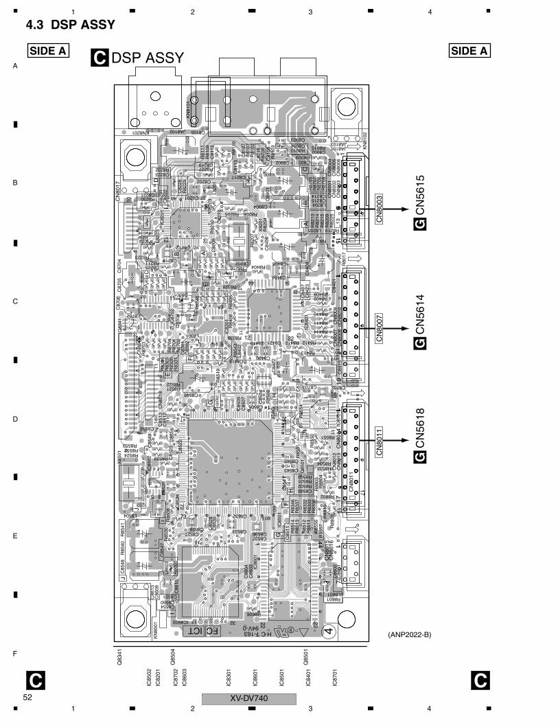
C
D
F
A
B
E
XV-DV74052
1 2 3 4
4.3 DSP ASSY
9
136
37
72
108
10
9
14
4
916
1 8
17 32
16 1
20110
1185
1
10
20
1 10
1
48 37
36
24
25
13
11
1
16
6 1
12
2
17
441
R82
25
R87
05
R87
08R
8706
R87
07
C84
23
CN
8001
D84
01C
N80
05C
N80
04
R85
54
R8232
R82
31
R8230
R82
29
JA8101
IC85
01
C83
02
IC83
01
R8411
KN
8501
IC8603
C86
10
C87
05
R8551
Q85
01
R8533
R85
31
R8534
R8503
R82
26
C8543
IC87
01C
N80
02
R83
45
C84
08C
8407
IC85
02
C85
25
R8206R82
03
R8211
C87
01
C8545
R8205
R82
04
C82
09
C89
01R
8103
C8405
C8404
C84
06
R8219L8205
C8904
C8902
C8215C8214
L8204
R82
13
R82
15R
8209
R82
14
R8015
X82
01
C84
22
CN
8010
R8416
R8413
R8412
R8414
CN
8007
R8553R8552
R8016
R80
17
R8410
R8409R8408D8501
C87
06
L8702
C87
04 C8225
CN
8017
C82
18
C8219
C8221
L840
2
C8419
C8418C8420
IC87
02
R85
50
CN
8008
IC84
01
C82
22
R8339
CN
8009
C8533
JA8103
C8532
KN
8102
IC82
01L8
203
C8217
C8212
C8213
C8201
C8202
L820
1C
8210
R8539
C8536C8537
R85
06
JA8102 C8105
C81
13
C86
03C
8604
C85
47
R85
43
KN8201
R8227
C8546
R83
35
R83
31R
8330
R83
29C
N80
18
C82
26
C85
49
R8522R8521
Q83
41
C85
15
C8516
CN
8006
R8524
R85
19
C83
01Q
8504
CN
8019
L8301
C8554
C85
09C
8507
C8223
R8222
R8223
KN
8101
R81
10
C8003C8004
C8001
C8002
C81
12
C81
07
C85
04
C8505
C85
13C
8512
C85
23 C85
22
R85
11R
8512
R85
13R
8514
R87
04
R88
10
R83
37
R83
36
R82
10
C85
24
R85
30 C8527C8526 C
8528
C85
30
R83
33R
8332
R82
07
R84
05R
8406
R8404
R8328
R8216L8202
CN
8003
R8009
R81
09
R81
07
R81
11 R8010
R81
02
R87
01R
8702
R87
03
C8703
C81
08
C8702
R85
56R
8557
CN
8016
CN
8013
C85
41
R83
46
R88
04
C86
01
R8501
CN
8011
C85
11
R88
03
R88
05
IC86
01 CN
8015
C8503R8502
R8802
R8601
C86
02C
N80
12C
N80
14
R8606
R86
08
R86
05
L860
3
C86
09
L8504
C8550C8551
C85
48R
8540
R85
41X
8501
C86
13
C84
15
C8421
L8601
A 13
B
33
34
FCICT 4
I
I
H
94V-0
FG
C
17
AE
G
H
11
F
E
J
JTA
G
23
H C T-163
B
C
1
19
D
D
J
IC85
01
IC83
01
IC86
03
IC87
01
IC85
02
IC87
02
IC84
01
IC82
01
IC86
01
Q85
01
Q83
41
Q85
04
159
73
144
1 8
9
20
10
15
14
5 8
115
1
1
11
1
12 22
44
115
1
23
36
121 9
12
2
17
11
22 23
11
191
17
DSP ASSYC
CN
5614
GC
N56
18G
C C
SIDE A SIDE A
CN
8011
CN
8007
CN
5615
GCN
8003
(ANP2022-B)
1 2 3 4
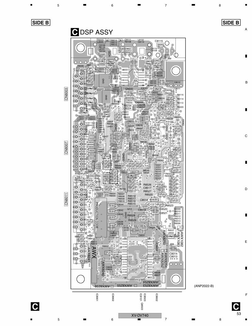
C
D
F
A
B
E
53
5 6 7 8
115
91
1915
14
8
13
119
C8555
L8005R8005
R8004L8004
R8003L8003
R8002L8002
D84
02 C8411C8410
R8234
R8233
R8228
C8605
C8009
R8504
R8529
R8528
R8555
R8807
R8808
R8806
R8809L8801
C8501C8502
R8510R8509R8508
C8542
C8544
L8701
R8114
C8403C8402
R8115
C8208
D83
03
R8202
R8407
C8204
C8207
L8401
IC8902
IC89
01
C8903
R8001L8001
R8019
R8105
R8417
C8114C8111R8108
R8507
C8417
C8416C8414C8413C8412
R8013
C8409
R8006
L8505
Q8503
D8503
D8502
R8538
R8547R8548
R8338
C8531
R8014
R8201C8203
L8501
R8224
C8534
R8526
C8535
R8104
C8115
R8112
R8515
IC8503
R8516
L8104
R8321R8320
R8340C8007
R8309
R8344R8308
R8310
L8502
C8607C8608
IC8602
R8311
R8536
R8523
R8520
R8505
R8545
D8301
R8549
R8527C8517
R8544
C8514
C8552
R8518R8517
R8542R8546
C8553
D8302
R8341
R8343
C8220
L8102
C8224
R8221
R8220
R8116IC8101
C8005
C8110C8109
L8103
C8006
C8521
C8520C8518
C8012
C8011
C8010
C8008
R8113
R8212
C8206C8205
C8529
R8018
R8403R8402R8401
R8334
R8008
R8532
R8007
R8011
R8012
C8104
C8106R8106L8101
C8211
C8216
C8540
C8539
R8811
C8538
R8801
R8602
R8603
R8812
R8813
C8606
C8014C8013
R8326R8314R8313R8312
R8558
R8537
R8322
R8415
C8401
L8602
BG
CH
AWX8239
V36
GN
DD
AWX8254
AW
XA
WX
8241
PR
OD
UC
TIO
N C
OD
E
AW
X8240
AW
X8252
A
177
1
GD
AC
GNDD
4
5
AW
X1082
8GN
DD
GN
DD
V11
C
C
AWX8253AWX8255
A
B
AW
X1083
AW
X8250
AW
X8251
Q8503
IC8902
IC8901
IC8503
IC8602
IC8101
IN
GN
D
OU
TIN
GN
D
OU
T
132
17 161
1417 8
DSP ASSYC
C C
SIDE B SIDE B
CN
8011
CN
8011
CN
8007
CN
8003
CN
8007
CN
8003
(ANP2022-B)
XV-DV7405 6 7 8
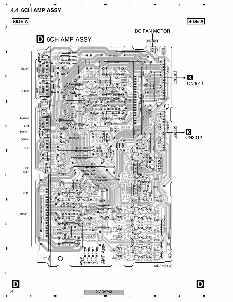
C
D
F
A
B
E
XV-DV74054
1 2 3 4
4.4 6CH AMP ASSY
1910
1
231
1
FLO
UT
1
word
surfa
ce
123
AW
M
SLOUT
GNDS
SWOUT
VA-12
GNDREG
SROUT
VD+5
VPF+15
VP+15
XPROTECT
VF-12
+B
GNDP
GNDP
VL+
VL-
IRFI
9Z34
G
-B
VL-
2SD
2012
NJM
7912
FAS
urfa
ceW
ord
IRFI
Z34G
D3393
W20
5D
3389
W19
8
R3388
W170
W143
W142
C3423W
147
W171
W190
IC34
01
W144
W14
6
W12
7
W197
Q61
D33
91
W11
1
W11
2
Q62
D3385
IC71
D3392
Q33
83
W182
W19
9
W181
W175
W180
Q33
84
D3387
D72
D3388
W20
2
C72
W200
W201
W18
3
W18
5
W20
7
R3387
D3386
W20
6C
63
W18
4
W203
W20
4
D3322
D33
90
D3394
231
1910
1
231
IRFI
9Z34
G
FLO
UT
SW
OU
T
SR
OU
T
123
wo
rd s
urf
ace
1910
1
1910
1
AM
P A
ssy
7788
GNDP
VH
+
VL+
VL-
NJM
7805
FA
123
FROUT
VH+
VH-
AW
M
-B
+B
GNDP
SLOUT
GNDS
GNDP
FR1S
P
Pro
duct
ion
Cod
e
Wor
d S
urfa
ce
UN
+8
VA
-12
FC
DC
7787
7786
7720
SWOUT
VA-12
GNDREG
SROUT
VD+5
VPF+15
VP+15
XPROTECT
VF-12
+B
-B
GNDP
GNDP
GNDP
VL+
VL+
VL-
+B
IRFI
9Z34
G
-B
VL-
Sur
face
IRFI
Z34G
D3393
R3318
D33
89
W19
8
R3388
W12
0
W170
W143
C3478
W138
W139
W140
Q91
W142
R3427
W141
W15
4
C3377
C3577
R3520
C3402
D3325
W123
C98
D3324
C3424
C91
C3317
C3578
C3423
C34
22
D98
D3328
W124
C3501
D3651 D3652
W104
D3653
D3654
W12
1
W126
D3326
W15
9
W151
W15
8
W105
W125
W14
5
W14
8
W14
7
D3323
W172
W171
W107
W173
IC81
C3301
D82
C36
52
C36
51
D36
55
W106
W10
9
W11
0
W108
W119
C3508
R36
57
Q36
54
W192
W122
C3653
W16
1
W195
W196
W194
W16
0
CN
3002
IC33
01
W190
W16
9
IC34
01
W16
8
D3427
D3428D3422
W18
7
W16
2
D3423
R3519
D3421
W16
7
R3517
W18
8
W166
R3417
W16
3
W150
C3323
C33
07
W144
W193
W14
6
W12
7
D3426
R3422
R3420
R3419
W19
1
W197
R3418W
164
D33
91
W12
9
C3408
C3507
D3424
W12
8
CN
3001
W11
1
W11
3
W13
0W
135
W11
2
W165
W18
9
Q62
C82
W10
3W
101
W117
D3385
D3425
IC71
W13
1
W13
2
C101
D3392
Q33
83
W149
W13
6
W11
6W
118
R3428
W115
W11
4
W13
3
W157
W177
W179
W176
R3421
W182
W178
W174
W19
9
W181
W175
W180
C34
07
C34
21
Q33
84
W137
D3387
D72
C3378
IC33
03
D3388
D3327
W20
2
C72 C33
22
R3328
R3327
C3318
W200
W201
W18
3
W18
5
W15
2
W20
7
R3387
D3386
W20
6
W18
4
C3179
W203
R3320
C102
C3167
R3317
W10
2
C3178
C3302
D3322
C3401
D3321
C3308
W15
3
C33
21
R3321
R3322
W155
R3518
C3502
C3324
D33
90
W156
C3477
D3394
R3319
C3168
SIDE A SIDE A
(ANP7461-A)
CN3012K
6CH AMP ASSYD
CN3011K
DC FAN MOTOR
IC81
Q61
Q3654
Q3383
Q3384
Q62
Q91
IC3401
IC71
IC3301
IC3303
CN
3002
CN
3001
CN3651
D D
1 2 3 4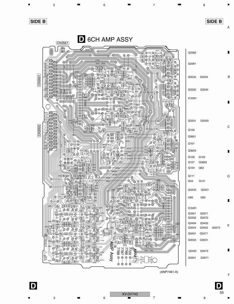
C
D
F
A
B
E
55
5 6 7 8
NP
NP
D
23
123
1
SWOUTSWOUT
VH+VH+
VH-
VH
+
VL+
VA-12VP+15
VD+5
VL-
TUNERXPRCT
GNDRGNDR
UN+8UN+8
GNDF
SLOUTSLOUT
VL+VL+
SROUTSROUT
VL-
VH-
VL-
FLOU
T
SW
OU
T
SR
OU
T
1
VH-
AM
P A
ssy
SROUT
GNDREG
GNDP
7788
COUT
FROUTGNDP
FROUT
COUT
IC3301
FROUT
VH+
FAN SIDE
FLOUTFLOUT
GNDS
GNDP
C2
E2
-B
GNDP
+B
GNDP
SWOUT
SLOUT
GNDS
GS
FR1S
P
VPR+8VPR+8
SRINSLIN
SWINCIN
FRINGNDA
SEN+8
FLINMUTE
MUTEC
VFL+5U
N+8
VA
-12
AW
M
772077867787
C1
B1
B2
E1
IC3401
VD+5
VPF+15
VP+15
XPROTECT
VF-12
VL+
VA-12
GNDP
+B
VL+
+B
GNDP
-B
VL-
GNDP
-B
VL-
1
BC
ES
DG
GD
S
C3509
R3511
R63
R3412C3410
R3411C3409
D3341
R3571R3513R3501
D104
R121
D3381
R3478
R3574
R3378
R3414
R3471
R3577
TH121
Q121
Q43
Q3433
R3377
D3443
R3443
R3439
R3435
R3576
Q92
D3441
R3345
R47
R45
D3582
R91
D91
C81 R46
R3476
Q3301Q3372
R3373
R3375
R3374R3376
C97
Q3371
C92
R3472
R3503
R95
R3426
R3416
R48
C3426
R92
R123
R114
R113
R3371
R111
Q111
R93
R96
R122
R3512
R97
R3313
R112
D3581
Q3653
R3301
Q3531
R3303
Q3652
R3651
D3657
R3506
TH111
D3658
R94
R3658
R3656
R3655
R3654
C3504
Q3651
Q107
R108
Q106
D42
R3307
R3509
R3507
R3505
Q3532
R3492
D3482
D3481
R3491
Q3432
R3531
C3503
R3545
C3305
R3316R3305
C3303
R3309
R3532
R3537
R3533
D106
R3543R3539
R3432
R3438R3434
R3591
R3424
R3538
R3575
R3451
R3534
R3544
R3540
R3592
D3382
C3506
C3406
Q101
Q102
Q104
Q103
C61
C3505
R3406
R3311
R3312
C3309
R3408
C3404
C71
R3351
C62
R3410
D3343
R109
R67
D102
R65
R3510
R3508
Q63
Q3431
R3431
R3437R3433
C3405
R3407
R3423
Q3434
R101
Q3501
Q3533
R3391
R3405
Q3401
R3392
C3403
C3510
Q3333
Q3334
R3409
R64
R68
R3340
R3344
D3344
R3343
R3383
Q3402
Q3504
R3339
C3310
R3334
Q3502
R103
Q3302
R3382 R3384
D105
R3386
R3332
D101
R62
Q3332
R61
R102
R3385
Q3382
R3390
R104
Q3331
R3326
Q3534
R105
R106
Q3381
D3544
R3381
R66
C3326
R3338
R3514
R3335
R3304
R3502
R3302
R3337
R3403
R3401
R3331
R3333
R3402
R3323
R3324
C3304
R3573
C3306R3310
R3306
R3308
R3404
R3389
D3543
Q3572R3572R3578
R3446
D3444
R3444
R3372
R3500
R3504
R3477
R3314
R3440
R3445
R3413
R3546R3346
Q3571
Q3471
Q3472
R3473R3475
R3474
SIDE B SIDE B
(ANP7461-A)
6CH AMP ASSYDC
N30
02C
N30
01CN3561
Q3332 Q3334
Q3532 Q3534
Q3381
Q3382
IC3301
Q102
Q3331 Q3333
Q3651
Q101
Q3653
Q106 Q103
Q107 Q3652
Q104
Q111
Q43
Q3433
Q92 Q92
Q3431
Q121
Q63
Q3533 Q3531
Q3501 Q3571
Q3402 Q3472
Q3401 Q3471
Q3504 Q3502 Q3572
Q3301 Q3371
Q3302 Q3372
Q3434 Q3432
IC3401
D D
XV-DV7405 6 7 8
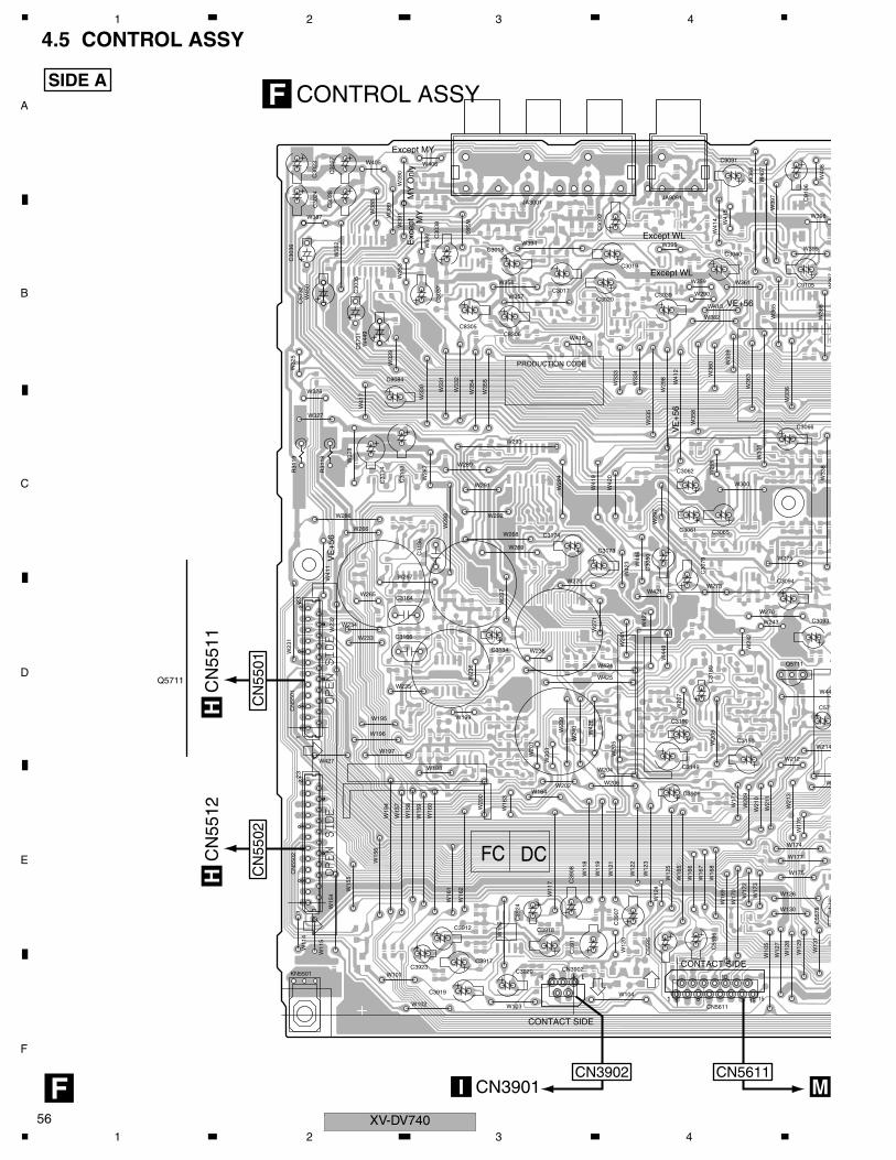
C
D
F
A
B
E
4
W40
8W
131
W12
9
W
W17
6
7
W36
6
W214
C3093
9105
C571
C91
06
75
W36
7W
338
C55
78
W399
W398
3066
1
W44
M
XV-DV74056
1 2 3 4
4.5 CONTROL ASSY
123
123
15
1
10
15
W243
W23
2
W23
6
W15
8
W15
9
W16
0
W15
7
C3919
W36
0
W15
4
W35
4
W35
5
W42
6
W33
6
W290
W195
W204
C3920
W202
C39
07
W292
C55
95
C39
08CN
5502
C9091
W17
W12
1
C90
92
W405
C30
24
W35
3
W33
3
C30
23
W29
8
R31
19
W28
7
C31
13
W24
2
W16
8
C3912
W23
7
W40
7
W101
W41
1
W33
5
W198
C55
96
CN
5501
W12
2
W35
8
C3065
W233
W29
9
W276
W20
7
JA9091
C3020
W39
2
R31
18
W275
W421
W291
C3019
C9084
C30
38
C31
89
W16
9
C30
27
W126
W17
1
C30
28
W38
9
W41
5
W273W
419
W212W
211
W15
5
C30
79
W12
3
C3039
C3040
W130
W326
W393
W300
W36
3
W395
W425
C3094
JA3001
W10
5
W23
1
C3150
W362
W39
0
CN3902
C3062
W29
4
C3166
C31
14
C3061
C3164
KN5501
W32
5
W17
W12
8
W32
8
W36
5
W20
3W269
C57
32
W15
6
W289
W12
0
W12
4
W266
W36
4
W12
7
C30
37
W11
9
W104
W20
8
W33
0W327
W17
3
W12
5
W20
5
W44
6
C57
31
W17
0
W361
W33
2
W21
3
W11
8
W293
W356
W268
C39
24
W265
W28
8
W270
C3923
W33
1
W39
7
W38
8
C
W23
9
W164
W19
4
W30
1
W24
0
W286
W102
C3134
W267
C3173
C3149
W11
4
W238
CN5611
C39
11
W27
1
W41
4
W33
4
W1
W33
9W196
W44
8
C3190
W206
W16
3
C3917
W35
2
W235
W17
2
W394
C30
80
W32
9
W29
7
W387
C8305W
115
W357
W199
W197
C8306
W11
6
W359
W234
W39
1
C3017
C
W406
C3174
W24
1
C3018
W20
0
W42
0
W16
5
W42
3
W427
C3918
W20
9
W20
1
C31
36
C3906
W103
W21
0
W16
6
W42
2
W16
7
W413
Q571
W418
W16
1
W41
2
W11
7
W424
W16
2
C30
36
C30
35
W45
0
W41
7W
449
MY
Except WL
DC
PRODUCTION CODE
FC
MY
Onl
y
Except MY
Exc
ept
Except WL
CONTACT SIDE
CONTACT SIDE
VE
+56
VE
+56
VE+56
Q5711
23
123
1
15
1 15
SIDE A
F
CONTROL ASSYF
CN3901I
CN
5511
H
CN3902 CN5611
CN
5501
CN
5512
H CN
5502
1 2 3 4
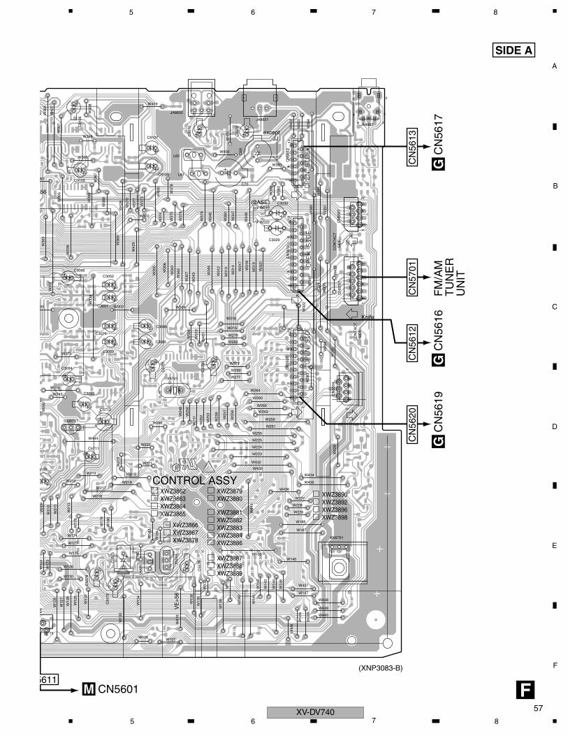
C
D
F
A
B
E
15
W243
W24
2
W40
7
W276
W21
1
300
W36
3
W10
5
3150
W36
5
W36
4W
173
361
W39
7
W30
1
W17
2W
209
W21
0
E
+56
15
5611
57
5 6 7 8
17
1 3
1
10
111
7
119
119
111
1
2
34
56
7
C57
05
W18
4
W434
W277
CN
5504
W43
1
JA8602
C70
W438
W33
6
W40
3
W32
4W316
X55
01
W224
W255
W174
W34
9
W38
0
W259
W35
0
C86
22
CN
5701
W228
CN
8301
W25
0
W40
8
W38
6
W34
6
W25
7
W45
1
W149
W260
W38
3
W25
8
W25
6
W34
1
W25
2
W13
1
W187
W25
1
W409
C3052
W34
3
C3086
C86
10
W13
9
W37
0
W264
W249
W222
W275
W432
W263
W262
W185
W13
3W
428
W31
0
W126
C5712
W12
9
W43
0
W219
W37
1
W37
3
W372
W42
9
W41
0
W37
5
W212
W31
2
W22
9
W37
6
W17
9
W216
W36
8
W106
W130
W14
2
JA8621
C3094
W223
W37
4
W226
KN5791
C3085
W31
9
W25
3
W279
W17
6
W177
W12
8
W36
6
W282
W148
W13
4
W24
8
W220
CN
5620
W12
7
W221
W225
W13
8
W32
1
C9107
W214
W34
2
W107
W21
3
C9108
W309
W400
W31
4
W37
8
W188
W37
9
W145
C3093
W34
8
CN
5612
W14
3
C9105
W32
0
C5711
C91
06
W10
8
W41
6
W32
2
W441
W13
6
W218
W31
8
W217
W14
4
W14
6
W28
4
W28
3
W13
5
W227
W14
0
CN
5613
W175
W36
7
W31
3
W33
8
W246
W38
2
W40
2
W30
8
W278
W14
1 W147
C55
78
W30
7
W399
W303
W398
W18
3
W34
5
W280
W36
9
W34
7
W28
5
W38
4
W35
1
C55
76
L557
1
C55
72
W21
5
C3066
X5701
W31
7
W261
W436
W30
6
W18
0
W18
2
W38
5
W30
5
W315
C55
75
W433
W437
W439
Q5711
W444
W381
L62
L61
C3029
C3030
C57
01
C3051
C3070
C3069
C69
JA8803
W44
5
W435
W440
XWZ3889XWZ3888
XWZ3898
XWZ3887
XWZ3890
XWZ3886
XWZ3881XWZ3882
XWZ3867
XWZ3892
XWZ3865
CONTROL ASSYXWZ3862XWZ3863XWZ3864
exceptJJ
XWZ3883XWZ3884
SID
EC
ON
TA
CT
SID
EC
ON
TA
CT
VE
+56
XWZ3866
Knife
(BASE)
XWZ3896
XWZ3878
XWZ3880XWZ3879
17
111
17
1
19
1
19
1
11
SIDE A
F(XNP3083-B)
CN5601M
CN
5617
GCN
5613
FM
/AM
T
UN
ER
U
NIT
CN
5701
CN
5616
GCN
5612
CN
5619
GCN
5620
XV-DV7405 6 7 8
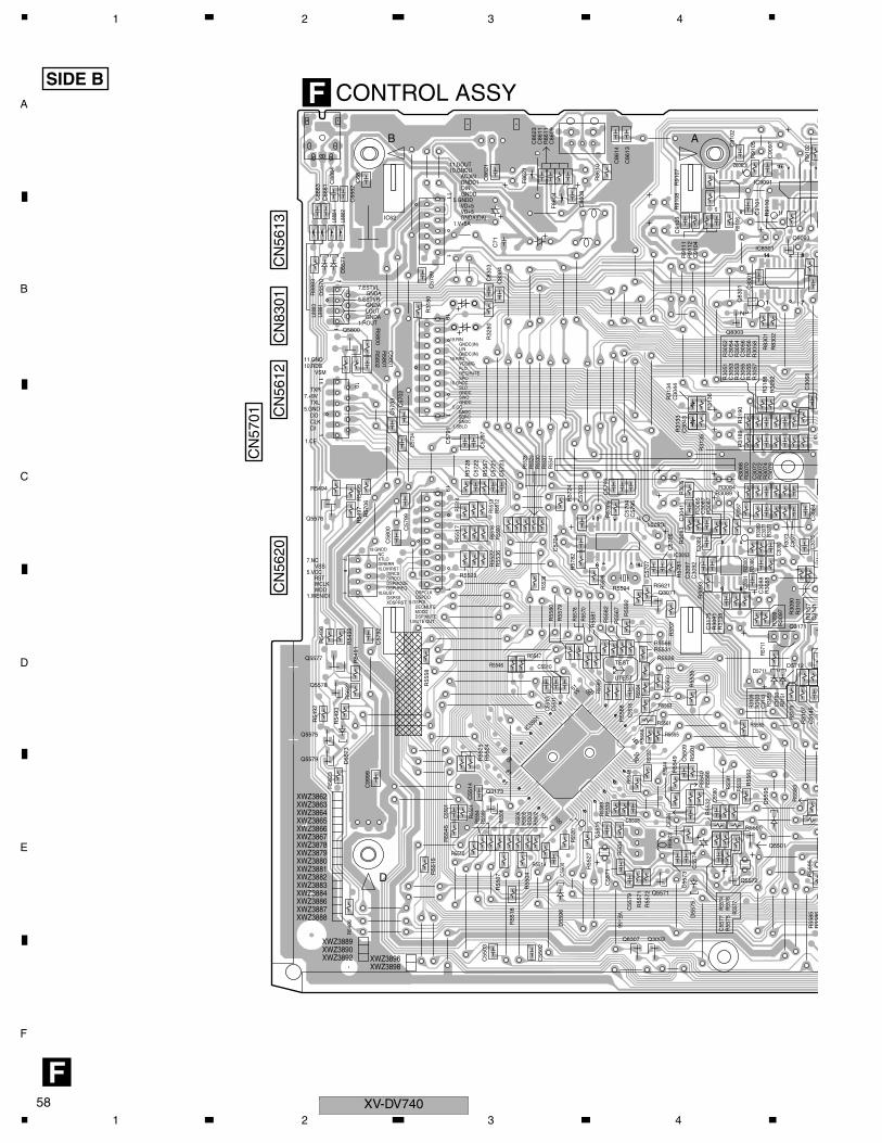
C
D
F
A
B
E
7
8
R91
02C
3068
R31
01
R55
86
R55
83
C30
84C
3141
R307
3R
3090
R55
95R
5585
Q3171
C307
7
R31
3
Q9093
R31
07R
3157
C31
45
Q
C30
75
R31
79
D5712
5
7
8
XV-DV74058
1 2 3 4
8 1
9 16
1
16
1
14
4 1
5 8
100
81
1
30
31
5051
80
R553
0
R55
25
C307
1
R30
57
C309
0
C55
01
R57
05
Q3071
R55
15
R54
93
IC5701
IC9091
D55
73
D55
70
Q5575
D55
71
Q5578
Q5579
R550
8
R55
27
C55
13
R86
10
R3084
R550
6
C30
56
C90
97
R91
11
R55
48
R555
0
L888
3
R55
20
R553
3
R55
39
C30
88
R91
12
R31
89
C30
53
C55
79
R31
90
R55
01
R55
24
R550
5
C86
23
R57
11
IC8301
L888
1
Q3003
R55
78
R308
6
R55
04
R83
01
R55
81
R56
01
C86
21C
5503
R550
9
C30
54R5
577
C55
02
R31
95R
5591
C55
80
R5565
C57
06
R55
22
C55
09
R83
02C
3193
R55
69
R30
99
R31
35
R32
80
R55
79
C57
03
F86
21
C309
1
L888
4
C86
08
R30
72
R5523
C5510
C31
75
F86
04
C30
92
R30
74
C30
55
R31
51
R55
07
R30
68
R31
36
R30
53
R31
33
C30
72
Q5576
R55
60
C86
11
R5561
C57
02
R5547
C30
89
R30
70
R5546
R55
67
C57
99
R5590
C30
87
R55
62
R55
89
C86
13
R30
88
IC3053
R307
1
C57
89
R306
9
Q83
01
Q5577
C5801
C83
01
C55
14
IC9092
R91
05
R30
87
R3089
Q5800
R30
85
R30
35
R555
4
R31
09
R91
06
D5711
C30
43R
9107
C86
09
Q8303
R91
08C
9103
R54
91
R5563
C57
92
R57
81
C55
15R
5599
C91
04
C550
4
R556
4
R55
68
R57
24
R553
7R
5580
R5594
C55
11
R552
9
R55
38
R55
35
R37
07 R30
97
C88
83
R55
36
R57
06
R55
18
R553
4
C550
6
R57
28
R30
91
C57
04
R55
82
R55
14
C55
16
C91
02
R55
92
R31
03C
9101
R54
98
R55
45
C88
81
R31
80
Q5571
R55
13
R31
34
C5508
C30
44
R54
99
C99
99
C31
43
R30
55
C57
91
R31
55R
3188
R30
58
C58
00
C57
23
R30
54
R55
49
C30
78
L888
2
R55
12R
5500
R554
1
R30
92
R86
11
R56
22
IC62
C86
14
C68
C57
21 R552
8
Q5572
Q8307
Q5501
R30
56
R30
52
C30
97
R55
16
C57
22
R55
40
R30
51
R550
2R5
503
R5526
C57
97
R330
0
C57
93
C57
95
R5621
R55
17
C83
03
R57
82
C83
04
R55
75C
5577
C55
71
R557
6
R55
73
R557
4
C55
73
R5510
R55
32
C57
07
C55
74
C57
94
IC55
01
R55
72R
5571
R30
93
R554
4
R55
57
R306
7R5555
R55
56
R55
70
C30
41
R5519
R30
83
R54
92
Q3173
R5531
R55
88
R5566
C88
82
C88
84
R5494
R91
10
R5801
R54
97
R5800
R5802
R54
95
C71
D55
95
R55
58
R88
83
D55
96
C57
33
C57
34
R54
96
D55
75
R56
23
B
7.NC
XWZ3896
XWZ3887
XWZ3883
XWZ3888
XWZ3889XWZ3890XWZ3892
GNDA1.ROUT
TEST
UTEST
7.ESTVLGNDA
5.ESTVRGNDALOUT
XWZ3881XWZ3880XWZ3879
XWZ3866
XWZ3864XWZ3863
XWZ3865
A
D
VE
+56
7.+9V
XWZ3898
XWZ3882
XWZ3862
XWZ3867XWZ3878
GNDA(DA)VD+5VD+5
5.GNDDGNDDDINGNDD1AC3IN
10.GNDU11.DOUT
1.MUTE OUTDSP MUTEMODCDECMUTE
5.DSPDIDSPDODSPCLK
XDSPRSTDSPSS
10.BUSYDSPHREQDSPMODEDIRDODIRCS
15.DIRRSTDIRERRXTLONC
19.GNDD
1.SBLO
5.GNDTXL
10.RDSVSM
TXR
1.CE
DI
DOCLK
11.GND
GNDCSBROGNDC
5.COGNDCSWOGNDCSLO
10.GNDCSRORECMUTEFLOVCOMG
15.FROGNDC(IN)LINGNDC(IN)
19.RIN
1.WEN/DIWDD
1.V+5A
XWZ3884XWZ3886
WCLKRST
5.VCCVSS
17
9 16
18
16
1
1
10
11
17
1
14
1
85
4
NP
85
4 1
119
19
111
1
1
30
31
5051
80
81
100
SIDE B
F
CONTROL ASSYF
CN
5613
CN
8301
CN
5701 C
N56
12C
N56
20
1 2 3 4
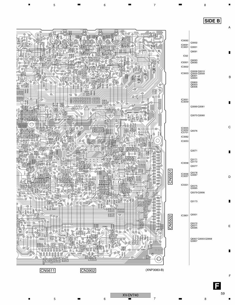
C
D
F
A
B
E
1
8
R30
57
IC90
84
C30
56R5
533
C30
88
R31
89
C30
53
R31
90
IC8
R308
6
C30
54R5
577
R5565
C309
1
R30
72
C30
55R
3068
R30
53
C30
72R
3070
R5590
R55
62
R306
9
Q83
01 C83
01
IC9092
R91
05
9
R31
09
R91
06
D571
8303
C91
02
R31
03C
9101
R30
55R
3058
R30
54
Q5572
R30
56R3
300
R306
7
1
8
NP
8
1
59
5 6 7 8
81
916
4 1
5 8
41
58
4 1
5 8
1 7
814
4 1
5 8
120
21 40
8 1
9 16
17
8 14
4 1
5 8
4 1
5 8
R31
05
C30
06
C307
1
R91
04
C31
69
R3106
Q8306
C309
0
R910
3
R30
14
R30
33
R30
34
R318
3R
3164
91
R32
05
R55
98
R5596
R30
19
R91
01
IC3051
F81
54
F81
56
C30
08R
3111
C90
97
Q3069
D39
02
C90
98
R301
6
C90
96
R84
02
R30
06
R30
21R3
020
C3111
R30
80
R91
02
IC3901
R90
95
R31
69R
3022
C312
4
R30
17
L300
6
R90
93
IC3057
R30
18
C31
22
R31
14
D3901
R30
78
R31
67
R31
76
C90
94
R31
20
R57
11
C30
05
C30
68
IC3052
301
R30
15
C31
77
C31
55
IC30
56
R83
01
C30
07
C31
94
R392
3
R30
04
Q3061
C30
76
C39
10
C31
48
L3005
L909
2
C31
80C
3179
R31
92
R83
02C
3193
R30
99
R31
22
IC3062
L300
4
R30
08
R30
36
R31
01
R30
10
R30
59
C31
33
IC3002
R39
24
C31
28
R30
13
R30
74
L300
8
R31
68
R31
51
IC3001
C31
17
Q3060
C31
23
R3002
C31
92
C316
8
R31
31
C319
1C3
909
C31
76
C30
67
R30
79
C312
5
R370
5
C31
21
C31
71
R316
2
R55
86
C31
16
R30
27R30
43
R5584
R3005
C30
09
R30
96
R3185
R55
83
R31
70
R32
13
C30
02
Q3907
R3044
R3172
R30
12
C30
83
C31
59
C30
60
C30
31R3
063
Q3908
IC3059
R30
28
R3939
C30
84
R3940
C316
5
C3032
R31
66
R31
59
C39
21
R31
13
L909
3
D30
03
C30
73
C31
41
R31
16
R30
88R3
071
R32
06
R31
38
L909
1
R31
15
C90
95
C31
56
C39
22
R31
39C
3004
R31
37
C30
10 L300
3
D30
04
R307
3
R31
17
R3187
Q30
04
L3002
D31
72
R30
90
R318
6
C39
13
R39
26R
3173
R30
09
R39
35
Q3065
C319
5
R318
1
R3163
R31
43
C83
02
R31
42
R31
52
R90
97
C30
01
R31
41
R31
40
R31
75
C31
38
R31
45R
3144
C3074
C31
15
D30
53
R39
21
R30
31
R32
07
D30
52
R39
25
R30
32
1
R31
12
C31
32
C31
53
R3024
R370
1
C31
12
C9093
R39
37
R55
95
R3023R30
25
R31
04
R32
14
C31
44
R3936 R393
8
R90
83
R55
87
R55
85
R55
51
R302
6
R31
25
IC3055
R30
11
R30
97
C30
03
R30
03
R31
71
C31
87
R31
82
C31
81
C31
78
C31
86
R32
08
R39
42
R31
65
L300
1
R315
8R
3941
R316
1
R303
0R3
029
R31
21
C30
25
R3703
R30
01
C30
26
Q3005
Q3171
R31
46
R30
39
R31
48
L300
9
R30
40
Q30
06
Q3070
R90
91R
3193
R39
22
C31
61
R57
31
R83
03
R90
89
Q3002
C307
7
C30
57
R30
60
R31
53
IC3003
C30
59R
3075
Q3001
L300
7
C31
47
Q3009
R306
1C3034
R57
32
C31
18
Q9093
C31
43
R30
07
R90
81
R370
6
C31
54
Q90
90
R83
04
R313
0
R31
32
R370
2
R30
47
R31
55R
3188
C316
3
R30
48
R370
4
R31
07
R31
29
R31
97
Q9091
R30
64
C30
78
R83
08
R30
62
C31
62
R31
74
R31
57
R30
77
R31
91
R30
92
Q30
10
Q3906
R90
82
R30
45
R3178
R83
07
R304
6
R30
49
R31
10
R31
08
R39
27C39
15
R39
28
C39
14
C31
45
C31
70
R30
50
Q5501
C31
37C
3033
R31
47
Q5595
R31
60
C30
58
C31
46
R31
56
C30
75
C314
2
R321
2
C31
60
R319
4
R315
4
C3126
R83
06
R31
23
R83
05
R3076
R31
84
R30
98
R321
1
R55
97
C31
30R
3126
C57
98
R31
96R
3124
IC3058
R31
77
R83
09
C31
31
R84
01
R31
28
R31
49
C39
16
R39
16
C31
72
C31
84C
3185
R3917R39
18
R39
29
R393
0
R39
33
R39
34
C31
35
C318
2C3
183
R31
27
Q31
72
R90
84
Q3067
R9109
R91
14
R91
10
R31
79
D31
71
R30
41R
3042
D91
00
R91
13
D55
95
D5712
FLIN
Q3070
Q3006
Q3171
Q3005
5
Q8303Q5800
Q3002
Q5571
Q3065
Q5577
Q3004
Q3908Q3907
Q5576
Q3060
Q8301
5.RYFSC
IC3058
SRIN20.SLIN
SWIN
DVDMUTENC
1.NC
GN
DLE
D15
.P_L
ED
T_LE
DV
E+5
RE
MO
10.K
EY
1FL
AC
2FL
AC
1G
ND
FLV
FL+5
5.FL
DA
FLC
KFL
CS
1.V
FDP
XFL
RS
T
CIN
23.SYPOWXDVDRST
5.M
UTE
GNDDGNDDGNDD
5.DOUTGNDUVE+56SUBACMUTE
HP
_DE
T
XVMUTE
GN
DA
HP
R
15.GNDAGNDA
DVDACK
10.FLAC1FLAC2
GNDFLVFDP
VPR+8/VD+5
VFL+515.MUTEC
XPROTECTMDATA
FRIN
VA+12
C
Q8307
1.HPACRYRVA-12
SDATASCLK20.VDETDON/OFF
VX+12GNDX
10.SYS_C1SYS_C2VD+5
Q9093
IC5501
IC62
IC3003
IC3055
IC9092
IC3053
IC3059
IC3001
IC3002
Q5575
1.H
PL
IC3062
IC3056
IC8301
IC3052
Q5578
IC3057
IC3901
IC3051
Q3061
Q3071
IC9091
IC5701
Q3067
Q3001
Q5572
Q3010
Q5595
Q8306
Q3173
Q9091
Q3009
Q5579
E B C
C B E
Q3172
Q9090
Q3906
Q5501
Q3069
Q3003
16
1
9
8
5
4 1
8
14
5
23
1
4
58
85
4 1
1 7
814
4
8
123
120
21 40
1
85
4
9 16
18
17
8 14
NP
1 5
1
0123456789 0123
0
01
CBA
85
4 1
4
58
1
1
10
15
85
4 1
SIDE B
F
(XNP3083-B)CN3902CN5611
CN
5501
CN
5502
XV-DV7405 6 7 8
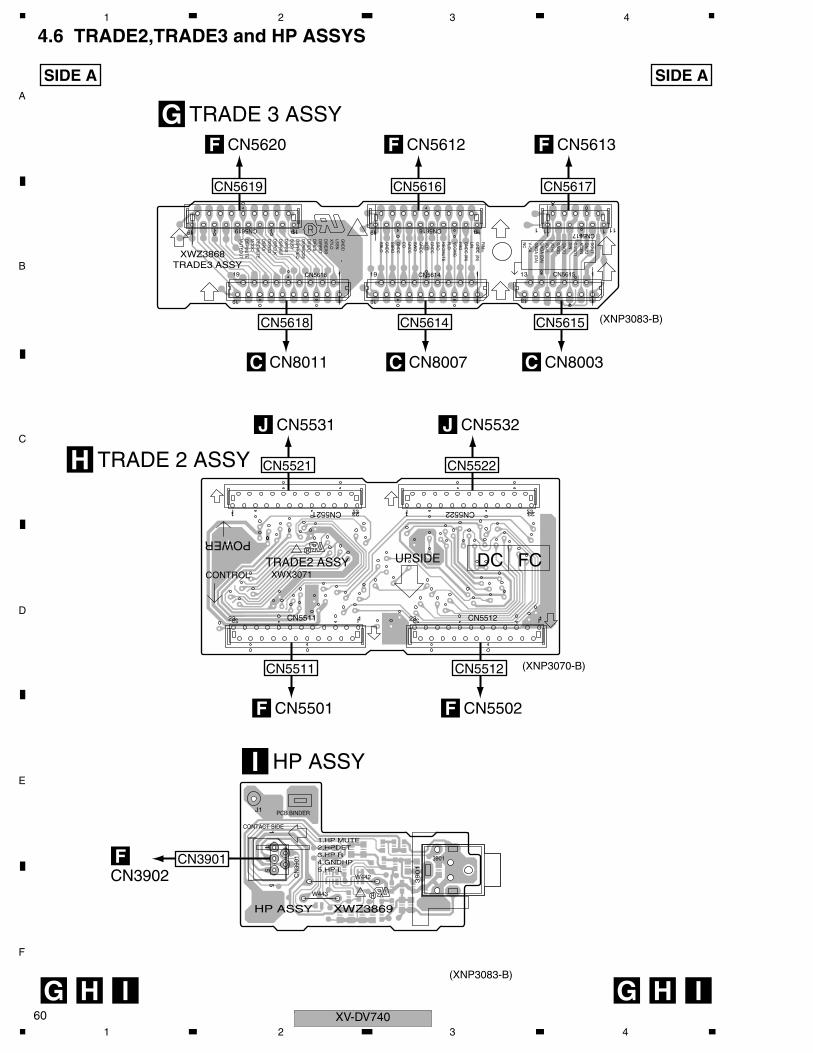
C
D
F
A
B
E
XV-DV74060
1 2 3 4
4.6 TRADE2,TRADE3 and HP ASSYS
119
15
113
119 111119
119
CN5618
W442
3901
CN
3901
W443
CN5615
CN5619CN5617
CN5616
CN5614
J1
5.HP L4.GNDHP3.HP R
XWZ3869
39
01
1.HP MUTE
HP ASSY
2.HPDET
CONTACT SIDE
SB
LO
TRADE3 ASSY
PCB BINDER
DS
PC
LKXWZ3868
DS
PS
SB
US
YD
SP
HR
EQ
DS
PM
OD
ED
IRD
OD
IRC
SD
IRR
ST
DIR
ER
RX
TLOLS
SN
AC
3IN
GN
DD
1D
IN
MO
DC
MU
TEO
UT
DS
PM
UTE
GN
DD
GN
DD
DS
PR
ST
VD
+5V
D+5
GN
DC
SB
RO
GN
DC
CO
GN
DC
GN
DA
(DA
)
V+5A
GN
DA
(DA
)
DO
UT
NC
DS
PD
O
DE
CM
UTE
DS
PD
I
SW
O
GN
DC
(IN)
GN
DC
(IN)
LIN
GN
DC
SLO
GN
DC
SR
OR
EC
MU
TEFLOV
CO
MG
FRO
RIN
GN
DU
GN
DD
19 1
51
113
191 1 11191
119
TRADE2 ASSY UPSIDE
POWER
CONTROL XWX3071
23 123 1
1 23 231
DC FC
CN5512CN5511
CN5521 CN5522
23 123 1
231 231
SIDE A SIDE A
G H I G H I
TRADE 3 ASSYG
TRADE 2 ASSYH
HP ASSYI
CN5620F
CN5619
CN5531J
CN5521
CN5532J
CN5522
CN5612F
CN5616
CN5613F
CN8003C
CN5617
CN5615
CN5502F
CN5512
CN5501F
CN3902F
CN5511
CN3901
CN8007C
CN5614
CN8011C
CN5618 (XNP3083-B)
(XNP3070-B)
(XNP3083-B)
1 2 3 4
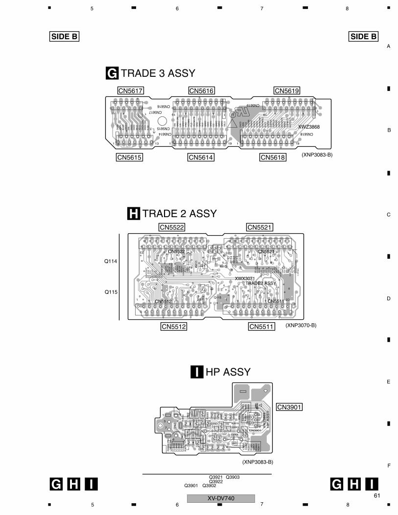
C
D
F
A
B
E
61
5 6 7 8
R39
06
R39
15
R39
62
R39
02
L390
3
R39
14
L390
2
L390
1
R39
03
C39
03
C39
01
R39
05
R3919
Q3903
R39
13
C39
05R
3907
R39
11
C39
04
R39
63R
3901
Q3921
C39
02
R39
08
R39
61
R39
64
R39
04C
3925
Q3901
R39
12
R39
20R
3909
6
7 HP
AS
SY
XW
Z3
86
9
5
4
3
2
1
CN3901
C B E
E B C
CN5618
SB
LOG
ND
CS
BR
OG
ND
CC
OG
ND
C
GN
DD
V+5
A
VD
+5G
ND
A (D
A)
GN
DU
DIN
AC
3IN
GN
DD
1
GN
DD
VD
+5 SW
O
GN
DA
(DA
)
GN
DC
SLO
RIN
GN
DC
(IN
)LI
NG
ND
C (
IN)
FR
OV
CO
MG
FLO
RE
CM
UT
ES
RO
XWZ3868GN
DC
CN5619
GN
DU CN5615
CN5614
CN5616
DS
PD
OD
SP
DI
DE
CM
UT
EM
OD
CD
SP
MU
TE
MU
TE
OU
T
GN
DD
LSS
NX
TLO
DIR
ER
RD
IRR
ST
DIR
CS
DIR
DO
DS
PM
OD
ED
SP
HR
EQ
BU
SY
DS
PS
SD
SP
RS
TD
SP
CLK
CN5617
NC
1 19
15
1 13
191
11 1 119
1 19
231 231
23 1123
FLIN
MU
TE
VA
+12
10.V
A-1
2G
ND
XV
X+
12
VD
+5
RY
R5.R
YF
SC
XWX3071
SW
INC
IN
MU
TE
C
FR
ING
ND
A
VE
+56
DV
DM
UT
ES
RIN
20.S
LIN
XD
VD
RS
T
AC
KV
DE
T
SY
_C
S2
SY
_C
S1
20.S
CLK
SD
AT
AM
DA
TA
15.W
AK
EU
P
GN
DF
LV
FL+
5V
FD
PS
YS
PO
W10.F
LA
C2
FLA
C1
SU
BA
CV
E+
56
GN
DU
5.D
OU
TG
ND
DG
ND
D
1.N
CGN
DD
XP
RO
TE
CT
UN
+8V
DV
DO
N/O
FF
15.G
ND
A
TRADE2 ASSY
1.H
PA
C
R11
1
Q114
Q115
R55
59
R11
2R
113
R11
4
CN5521CN5522
CN5512 CN5511
SIDE B SIDE B
G H I G H I
TRADE 3 ASSYG
TRADE 2 ASSYH
HP ASSYI
CN5619
CN5521CN5522
CN5616CN5617
CN5615
CN5512 CN5511
CN3901
CN5614 CN5618 (XNP3083-B)
(XNP3070-B)
Q114
Q115
(XNP3083-B)
Q3921Q3922
Q3902Q3901
Q3903
XV-DV7405 6 7 8
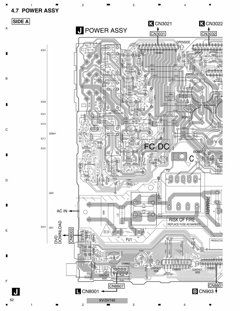
C
D
F
A
B
E
4
1
2
D36
W175
W177
W196
W217
33
35
34
W125
1
DUCTIO
UN+8
VD+5
022
2
8801
XV-DV74062
1 2 3 4
4.7 POWER ASSY
17
145 9
123 23
12
5
1
1 9
1
10
17
12
6
7
12
13
14
1
C3632
C8821
R3361R
3607
L3361
RY
3643R
Y3641
CN
8003
C23
C
T2
C51
C1
W114
H1 H2
R1
AN
1
CN3031 CN3032
R3631
R3632D
3631
D3634
D3633
L3362
R3362
R3561
L3561
RY
3642
R3661
L3661
L3461
R3461
R3462
L3462
C24
R3608
R3627
R3628
R3617
R3618
Q3641
C8831
C15
CN
8802JA
8803
W229
W215
W174
W232
W185
W172
W187
W144
W164
W168
W194
W212
W211
W156
W236
W169
W170
W213
W214
W191
W189
W124
W231
W161
W141
W171
W210
W165
W192
W143
W186
W145
W228
W158
W2
W146
W230
W2
W193
W173
W134
W129
CN8807
KN
2
C3631
CN8803
W130
W2
W133
W159
W227
W147
W166
W157
W188
C3633
W195
JA3301
W167
W142
W120
W155
W116
W119 W
121
W131
W241
W240
L1
W154
CN880
W216
W104
W250
BOND
1
GNDSPGNDSP
VH+
C
PRO
PRIMARY
RISK OF FIRE
GNDSP
9 pin
CONTACT
IC12
VD+5
IC21
IC22
1
IC31
IC11
IC61
IC51
GNDSP
FU1
OPENSIDE
OPENSIDE
7
CONTACT
1SIDE
GNDFL
GNDFR
GNDSL
GNDSL
GNDSW
GNDC
123
GNDP
VH-
GNDS
VL-
GNDFAN
UN+8
VH-
VH-
VH+
VL-
VL+
VL-
REGG
ND
XPROTECT
DVDPOW
ER
RYR
GND
VD+5
VD+5
SLOUT
GNDSR
VH+
FROUT
REPLACE FUSE AS MARKED.
CONTACT
FC DC
17
5 pin
ASPECT
Q3641
C GNDV
SIDECONTACT
SIDE
1 9SIDE
Q32
V
V+12M
BOND
VD+5
UPPER
Q51
1
18
SIDE A
J
POWER ASSYJ
CN903B
CN3K
CN303
CN3021K
CN3031
DV
DD
OW
NLO
AD
CN
8003
CN
AC IN
CN8001LCN8807
1 2 3 4
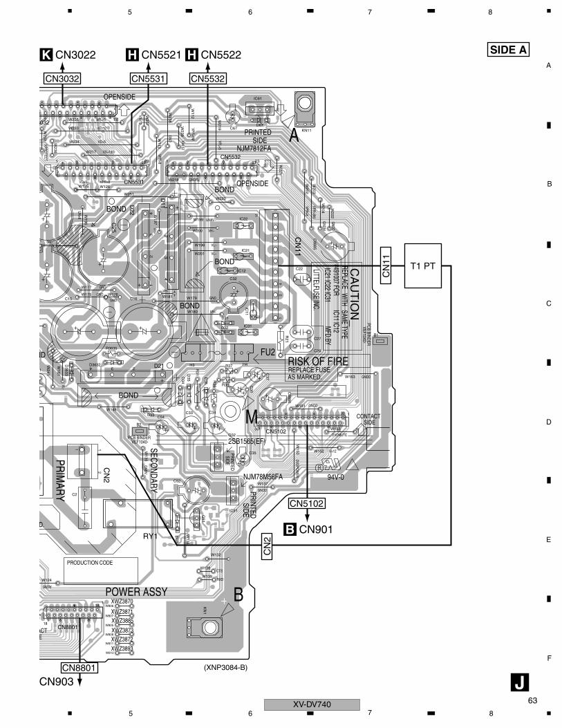
C
D
F
A
B
E
1
1
3032
W232
W236
W124
W161
W241
C
PRIMARY
XPROTECT
GND
D.
GNDV
EACT
ND
1
18
CN9
CK
CN3
63
5 6 7 8
12
34
1234
13
4
1
1 23
1
1 23
30
1
12
34
18
D31
D32
C32
KN11
D22
D21
CN
11R
21
R37
R36
D36 R
35
D35
R31
C35C
N2
C2
C52
RY1 D52
IC51
C54
KN
1
C33
C26
CN5532
R3635
D3632D3633
D33
D34
C36
C37
C25
IC61
C67D67
W808
Q51
W151
C15
W152
W175 W181
W126
W180
H4
W202
W805
W179
W198
C16
W218
W238 W
219
W251
W177
W200
W196
W176
W217
CN5531
W113
W233
W153
W235
W239
W203
W148
W234
W806
W204
C22
H3
W199
W221
IC11
C8885
C34
W201
CN5102
W136
W222
W139
W150
W237
IC31
IC22
IC21
IC12
W220
W812
W811
C8886
W137
W163
W807
W112
W132
W138
C27
W125
D11
W135
N8801
W197
Q32
AS MARKED.
BOND
FU2
XWZ3870
PCB BINDER
GNDD
BOND
BOND
DVDMUTE
DVDPOW
ER
VX+12
RXD
VD+5
GNDD
PRODUCTION CODE
SECONDARY
XWZ3871
A
VH~
GNDV
23
VH~
CTS
PRINTEDSIDE
PRINTEDSIDE
OPENSIDE
OPENSIDE
CONTACT
XWZ3873
UN+8
VPR+8
GND
GND
GND GND
VH+
VL-
GNDD
GNDM
V+12
VFL+5
VFL+5
VH-
VPR+8M
VPR+8
VX+12
VA+12
VF+12
GND
VD+5
NJM78M56FA
NJM7812FA
BOND
VEF1040-
VPR+8M
XWZ3872
VEF1040-
POWER ASSY
XWZ3885
M
GNDD
B
UN8V~
VL~
VL~
GNDFL
IC11 IC12IC21 IC22 IC31
LITTELFUSE INC.
MFD.BY#491007 FOR W
ITHSAME TYPE
REPLACEC
AU
TIO
N_
PCB BINDER
94V-0
231
VPR+8
RISK OF FIRE
BOND
XWZ3893
REPLACE FUSE
B2
B1
SIDE
SIDEPRINTED
2SB1565(EF)
110
12
23
1
30
1
SIDE A
J(XNP3084-B)
03
CN5522H
CN5532
T1 PT
CN5521H
CN5531
N3022
032
CN901B
CN5102
CN8801
CN
11
CN
2
XV-DV7405 6 7 8
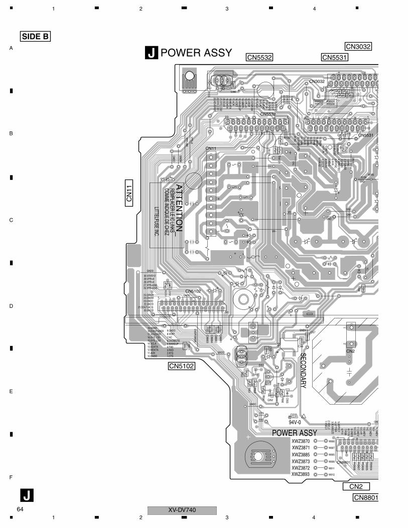
C
D
F
A
B
E
R9905
R9904
VL-
17.GNDV
5531
14.C13.G
NDV
15.GNDV
GND
W19594
16.V
1
2
8801
XV-DV74064
1 2 3 4
C8881
C8882
Q52
R55
R53
D51
R56
R52
R51
C53
C57
C56
C58
R9505 R9504
C66
C8883
R9501
Q131
R9503
D53
R54
D103
R9906
R9907
R9908
L3701
R3701
C8884C
9901
D55
TH
131
R132
R133
R131
UN+8
GND
GND
GND
GND
VH+
GNDD
GNDM
30
CN8801
COMME INDIQUE.DE CHEZ
6.P/XI
8.CY/G7.RG
B
5.ASPECT4.LETTER3.SQ
UEEZE
VH~
CN
VH-
SECONDARY
CTS
123
9.GNDV
11.GNDV
12.Cr/R
10.Cb/B
1.HPAC2.XTUNER3.UN+8V4.XPRO
TECT5.RYFSC6.RYR7.VD+58.VX+129.G
NDX10.VA-12
11.VA+1212.M
UTEC
13.MUTE
15.GNDA 14.FLIN
16.GNDA
17.FRIN18.CIN19.SW
IN20.SLIN21.SRIN22.DVDM
UTE23.NC
13.VFL+5
1.NC
2.GNDD
3.GNDD4.G
NDD5.DO
UT6.G
NDU7.VE+568.SUBAC9.FLAC1
10.FLAC2
11.SYSPOW
12.VFDP
14.GNDFL
15.WAKEUP
16.VDET17.ACK18.M
DATA19.SDATA20.SCLK21.SYS_CS222.SYS_CS123.XDVDRST
8.VDET9.GNDD
10.GNDD11.ACK12.MDATA13.SDATA14.SCLK15.SYS_CS216.SYS_CS117.XDVDRST18.DVDPOWER19.GNDD
20.GNDD21.DOUT(AC3)
22.GNDD23.GNDD24.GNDM
26.VPR+8(M)
25.GNDM
27.VPR+8(M)
29.VPR+828.VPR+8
30.VDVD12
1.CTS2.RTS3.RXD4.TXD5.WAKEUP6.DVDMUTE7.NC
1
2.VSEL21.VSEL1
1
CN3032
GNDV
RXD
LITTELFUSE INC.
W1
94V-0
DVDMUTE
REMPLACER LE IC LINKS
GNDC
GNDD
GNDD
GNDD
VPR+8M
VPR+8
V+12
AT
TE
NT
ION
_
DVDPOW
ER
CN5102
CN11
CN2
W812
W806
W808
W805
W807
XWZ3873XWZ3885XWZ3871XWZ3870
W811
POWER ASSY
CN5532
XWZ3872XWZ3893
110
12
+ -
~ ~
123 23
SIDE B
J
POWER ASSYJ CN5532 CN5531
CN303
CN5102
CN2
CN
CN
11
1 2 3 4
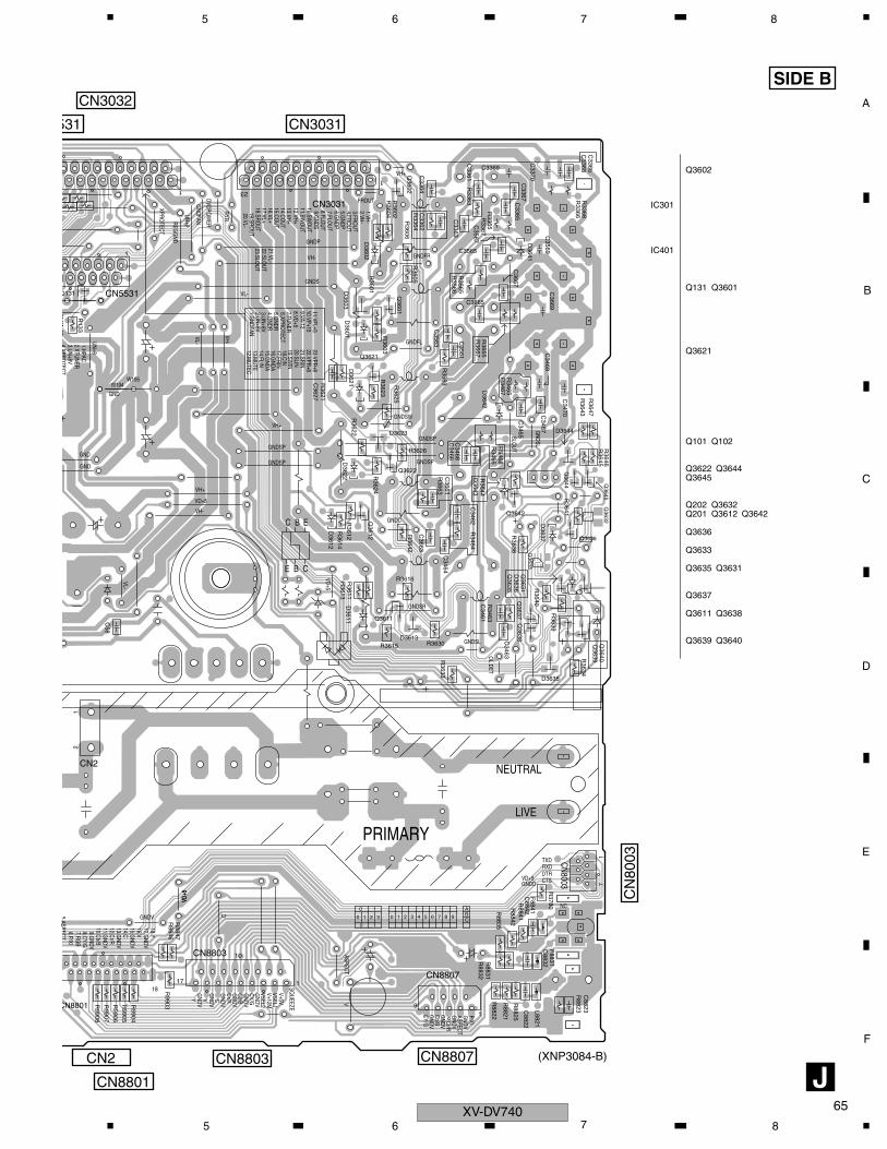
C
D
F
A
B
E
Q131
R133
UN+8
GND
GND
CN8801
6.P/XI
8.CY/G7.RG
B
5ASPECT
9.GNDV
1.HPAC2.XTUNER3.UN+8V4
XPROTECT
11VA
12
CN2
12
531
CN
C
65
5 6 7 8
R3638
C8842
C8832
C8823C
8822C
3370
C3363
C3361
R3363
R3605
R3601
R3366
R3615
R3644
R3642
R3643
D3641
D3602
R3604
C3367
C3365
C3368
C3366
C3567
C3565
C58
R3633
R3634
R3646
D3635
D3603
D3623 D3644
R3641
R3645
D3637
C3362
R3364
C3364
R3602
R3603
D3601
R3606
C3369
C3569
R3365
R3565
R3625
R3621
D3642
C3561
R3563
C3563
C3663
R3663
C3661
R3626
R3622
R3623
R3624
D3622
D3621
C3470
C3469
C3669
C3468
C3467
C3667
C3465
C3466
C3665
R3466
R3465
R3665
C3461
R3463
C3463
D3643
C3462
R3464
C3464
R3611
R3616
D3613
R3612
R3614
D3612
R3613
D3611
D3636
R3667
R3367
R3647
C3627
Q3631
Q3611
Q3612
Q3642
Q3644
Q3621
Q3622
Q3601
Q3602
R3467
Q3635
R3566
Q3636
Q3645
Q3633
Q3632
R3468
R3368
Q3637
R8821
R8822
R8823
R8831
R8832
R8841R
8842R8846
R8847
L8821
F8831
F8841
Q3638
Q3639
Q3640
R3639
R3630
R3640
R8825
R9903R
9905
R9906
R9907
R9908
R8835
R3780
R9904
VD+5
GNDC
GND
VH-
VL-
GNDFAN
XPROTECT
REGG
ND
UN+8
DVDPOW
ER
RYR
VD+5
GNDSL
GNDSL
SLOUT
GNDSR
GNDSW
GNDFL
VL-
GNDS
VH-
GNDP
VH+
FROUT
GNDFR
CN8803
OL DET
VSEL1
VH-
GNDV
GNDV
VL-
VH+
Cb/B
1
Cr/R
NEUTRAL
CY/G
VH+
17.GNDV
CN5531
PRIMARY
18.Y
18
14.C13.G
NDV
11.GNDV
12.Cr/R
15.GNDV
10.Cb/B
1.VH-2.VH-3.FRO
UT4.FRO
UT5.G
NDP
7.FLOUT
8.FLOUT
9.GNDS
6.GNDP
10.SWO
UT11.SW
OUT
12.VH+13.VH+14.CO
UT15.CO
UT16.VL+17.VL+18.SRO
UT19.SRO
UT20.VL-
21.VL-22.SLO
UT23.SLO
UT1.G
NDFAN2.UN+8V3.UN+8V4.G
NDR5.G
NDR6.XPRO
TECT7.TUNER
11.VFL+5
8.VD+5
10.VP+159.VA-12
12.MUTEC
13.MUTE
14.FLIN15.G
NDA16.G
NDA17.FRIN18.CIN19.SW
IN20.SLIN21.SRIN22.VPR+823.VPR+8
23
1
P/XIG
NDV
GNDV
GNDSP
NC
GNDDVD+5 CTS
DTRRXDTXD
E
E B
BC
C
GNDSP
CN8807
LIVE
W195W194
VD+5
CN8003
ASPECT
VSEL2
ASPECT
GNDSP GNDSP
GNDV
SQUEEZE
V+5V
V+12M
CY/G
GNDV
Cb/B
GNDV
Cr/R
GNDV
CG
NDV
GNDV
Y
16.V
VG
NDV
C
V
CN3031
19
VD+5 Q202
Q101
Q201
Q3640Q3639
Q3638
Q3637
Q3632
Q3633
Q131
Q3645
Q3636
Q3635
Q3602
Q3601
Q3622
Q3621
Q3644
Q3642Q3612
Q3611
Q3631
IC401
Q102
IC301
17
1
1
10
17
1
0 1 2 3 4 5 6 7 8 90 1 2 3
0
0 1
CBA
SIDE B
J(XNP3084-B)
3032
CN3031
CN
8003
N2
CN8801
CN8803 CN8807
XV-DV7405 6 7 8
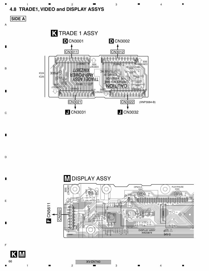
C
D
F
A
B
E
V56017
XV-DV74066
1 2 3 4
4.8 TRADE1, VIDEO and DISPLAY ASSYS
123
1 23
123
1 23
CN3012
W304
CN3022
CN3011
CN3021
W307
W306W303
W308
W302
W301
W305
IC25
W309
CONTACT
CONTACT
CONTACT
CONTACT
SIDE
LITTELFUSE INC.
TRADE1 ASSYAMP-POWER
XWZ3877
94V-0
SIDE
IC25 MFD. BYTYPEREPLACE WITH SAMECAUTION_SIDE
#491007 FOR
SIDE
UPSIDE
4910077A 125V
1 23
123
231
1 23
62
1
15
1
L5562
C5564
D5932
W502
CN5601
W505W
503
W504
C5953
W506
D5561
C5679
5951
S5927
W501
S5926
6.KE
Y
94V-0
15
PLAY/PAUSE
XWZ3874
13.FLCS
5.RE
MO
CO
N
7.FLAC
1
12.FLCLK
4.VE
+5V
E+5
9.GN
DFL
14.XFLR
ST
11.FLDA
TA10.V
FL+5
SIDECO
NTACT
OPN/CLS
8.FLAC
2
DISPLAY ASSY
15.VFD
P
1.NC
3.TIME
RLE
D2.G
ND
LED
1
62 358
1
SIDE A
K M
(XNP3084-B)
IC24
IC25
TRADE 1 ASSYK
DISPLAY ASSYM
CN3001D
CN3011
CN3002D
CN3012
CN3032J
CN3022
CN3031J
CN3021
CN
5611
F CN
5601
1 2 3 4
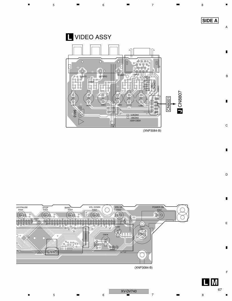
C
D
F
A
B
E
S5926LAY/PAU
67
5 6 7 8
1V5601
S5925 S5922
D5931
D5662
W507
C5678
L5563
S5921S5924
C5680
S5923VOL UP POWER ONVOL DOWNSE BANDSTOP
1
15
31
37
1
2
8
9
19
W140
C8871C8961 C8861
JA8951
CN8851
W128
CN
8001
C8951 C8851C8971
SIDE
51
Y(GREEN)Cb(BLUE)
CONTACT
XWZ3875XWZ3891
4.CbGND
Cr(RED)
9.P/XI8.GNDV7.ASPECT
1.Y
94V-0
2.YGND
6.GNDV
VIDEO ASSY
3.Cb
5.Cr
5pin
9
9pin
SIDE A
ML
(XNP3084-B)
(XNP3084-B)
VIDEO ASSYL
CN
8807
JCN
8001
XV-DV7405 6 7 8
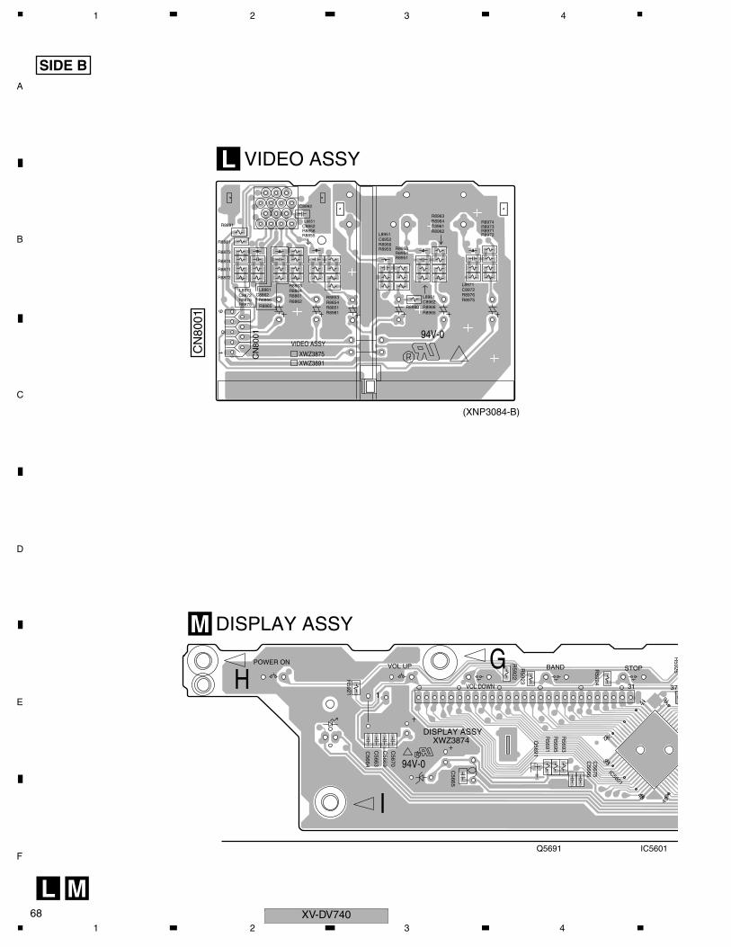
C
D
F
A
B
E 16
49
R5925
37
16
49
601
XV-DV74068
1 2 3 4
17
32
33
48
R5695
R5922
R5693
C5675
R5924
C5663
C5664
IC5601
C5665
C5666
C5670
C5669
Q5691
R5923
R5691
R5921
POWER ON
1
STOP
XWZ3874DISPLAY ASSY
VOL UP
VOL DOWN
BAND
94V-0
I
HG
3117
32
33
48
R8963
L8951
R8974
R8866
R8980
C8952
R8954
R8961C8852
R8966
R8955
R8854
R8863
R8861
R8874
R8891
R8871
R8864C8862
R8964
R8971
L8861
R8872
C8962
L8871
R8873
R8865R8875R8862
R8972
R8951
L8961R8876
R8965
C8872 R8853
R8962R8856R8855
L8851
R8881
R8976
R8851
R8973
R8953
C8972
C8992
R8981
R8956
L8971
R8975
XWZ3891
VIDEO ASSY
XWZ3875
94V-0
CN
8001
19
SIDE B
L M
DISPLAY ASSYM
Q5691 IC5
(XNP3084-B)
VIDEO ASSYLC
N80
01
1 2 3 4
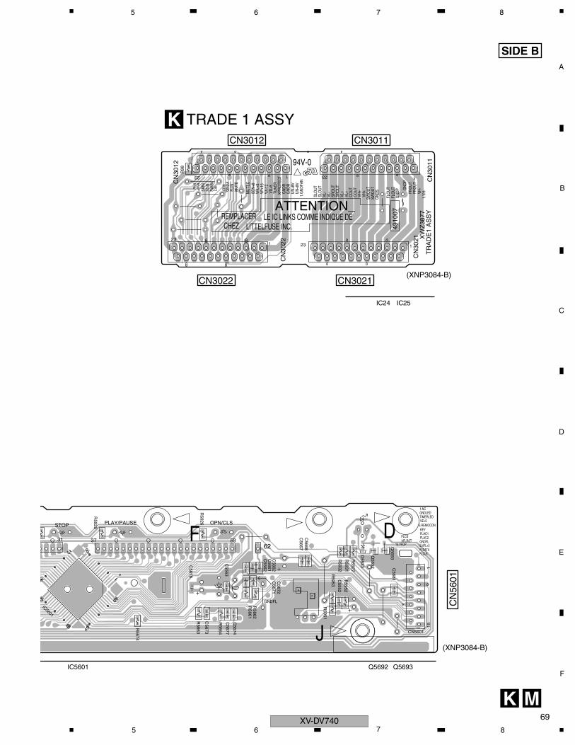
C
D
F
A
B
E
32
33
IC5601
ST
31
32
33
69
5 6 7 8
R98
1.G
NDFA
NUN
+8V
SEN+
8
VA-1
2VP
+15
VD+5
VFL+
5
TUNE
RXP
ROTE
CTG
NDR
GND
RUN
+8V
MUT
EC
MUT
EFL
IN
23
CN
3021
1
GND
A
CIN
FRIN
1.VH
-VH
-FR
OUT
FRO
UTG
NDP
GND
PFL
OUT
FLO
UT
GND
SSW
OUT
SWO
UTVH
+VH
+CO
UTCO
UTVL
+VL
+SR
OUT
SRO
UTVL
-VL
-
SLO
UTSL
OUTSW
INSL
INSR
INVP
+8VP
+8
94V-0
CN
3022
CN
3012
CHEZ
XW
Z38
77C
N30
11
4910
07LE IC LINKS COMME INDIQUE DELITTELFUSE INC.
REMPLACERATTENTION_
TR
AD
E1
AS
SY
123
123
123
1
1617
48 49
64
R5931
R5951
Q5692
R5953
R5662
R5663
C5563
C5674
R5952
C5672
C5667
R5926
C5662
C5562
C5676
C5668
R5674
C5673
R5925
D5933
C5681
R5661
C5671
R5927
Q5693
C5677
C5661
R5932
R5664
C5952
CN5601
FLCS
5.REMOCON
FLAC1
FLCLK
VE+5
GNDFL
62
GNDFL
OPN/CLS
GNDLED
KEY
TIMERLED
OP
FLAC2
10.VFL+5FLDATA
1.NC
15.VFDP
PLAY/PAUSE
XFLRST
J
F D37 58
115
1
1617
4849
64
SIDE B
MK
(XNP3084-B)
(XNP3084-B)
TRADE 1 ASSYKCN3011CN3012
CN3022 CN3021
CN
5601
IC25IC24
Q5693IC5601 Q5692
XV-DV7405 6 7 8
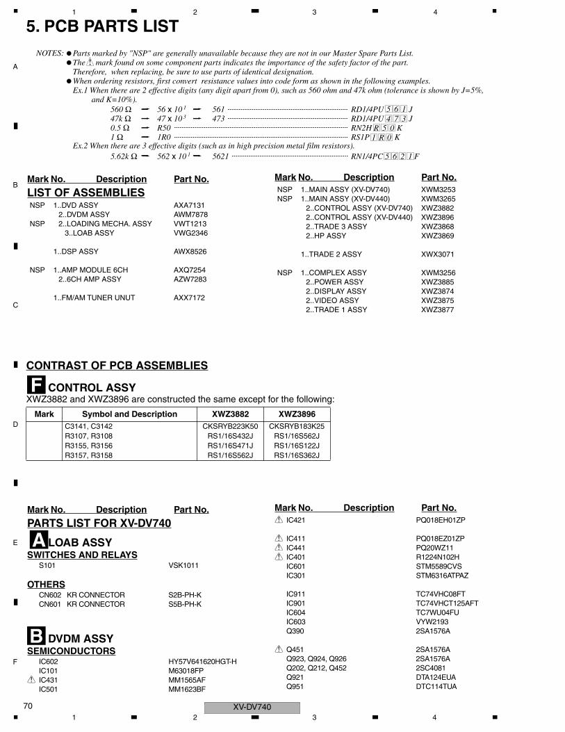
C
D
F
A
B
E
XV-DV74070
1 2 3 4
5. PCB PARTS LIST
CONTRAST OF PCB ASSEMBLIES
XWZ3882 and XWZ3896 are constructed the same except for the following:
Parts marked by "NSP" are generally unavailable because they are not in our Master Spare Parts List.The mark found on some component parts indicates the importance of the safety factor of the part.Therefore, when replacing, be sure to use parts of identical designation.When ordering resistors, first convert resistance values into code form as shown in the following examples.Ex.1 When there are 2 effective digits (any digit apart from 0), such as 560 ohm and 47k ohm (tolerance is shown by J=5%, and K=10%).
Ex.2 When there are 3 effective digits (such as in high precision metal film resistors).
5 6 14 7 3
R 5 01 R 0
5 6 2 1
NOTES:
560 Ω47k Ω0.5 Ω1 Ω
RD1/4PU JRD1/4PU JRN2H KRS1P K
56 x 10 1
47 x 10 3
R501R0
561473
5.62k Ω RN1/4PC F562 x 10 1 5621
Mark No. Description Part No.
LIST OF ASSEMBLIESNSP 1..DVD ASSY AXA7131
2..DVDM ASSY AWM7878NSP 2..LOADING MECHA. ASSY VWT1213
3..LOAB ASSY VWG2346
1..DSP ASSY AWX8526
NSP 1..AMP MODULE 6CH AXQ72542..6CH AMP ASSY AZW7283
1..FM/AM TUNER UNUT AXX7172
NSP 1..MAIN ASSY (XV-DV740) XWM3253NSP 1..MAIN ASSY (XV-DV440) XWM3265
2..CONTROL ASSY (XV-DV740) XWZ38822..CONTROL ASSY (XV-DV440) XWZ38962..TRADE 3 ASSY XWZ38682..HP ASSY XWZ3869
1..TRADE 2 ASSY XWX3071
NSP 1..COMPLEX ASSY XWM32562..POWER ASSY XWZ38852..DISPLAY ASSY XWZ38742..VIDEO ASSY XWZ38752..TRADE 1 ASSY XWZ3877
Mark No. Description Part No.
FCONTROL ASSY
Mark Symbol and Description XWZ3882 XWZ3896C3141, C3142 CKSRYB223K50 CKSRYB183K25R3107, R3108 RS1/16S432J RS1/16S562JR3155, R3156 RS1/16S471J RS1/16S122JR3157, R3158 RS1/16S562J RS1/16S362J
Mark No. Description Part No.
PARTS LIST FOR XV-DV740
ALOAB ASSYSWITCHES AND RELAYS
S101 VSK1011
OTHERSCN602 KR CONNECTOR S2B-PH-KCN601 KR CONNECTOR S5B-PH-K
BDVDM ASSYSEMICONDUCTORS
IC602 HY57V641620HGT-HIC101 M63018FP
> IC431 MM1565AFIC501 MM1623BF
> IC421 PQ018EH01ZP
> IC411 PQ018EZ01ZP> IC441 PQ20WZ11> IC401 R1224N102H
IC601 STM5589CVSIC301 STM6316ATPAZ
IC911 TC74VHC08FTIC901 TC74VHCT125AFTIC604 TC7WU04FUIC603 VYW2193Q390 2SA1576A
> Q451 2SA1576AQ923, Q924, Q926 2SA1576AQ202, Q212, Q452 2SC4081Q921 DTA124EUAQ951 DTC114TUA
Mark No. Description Part No.
1 2 3 4
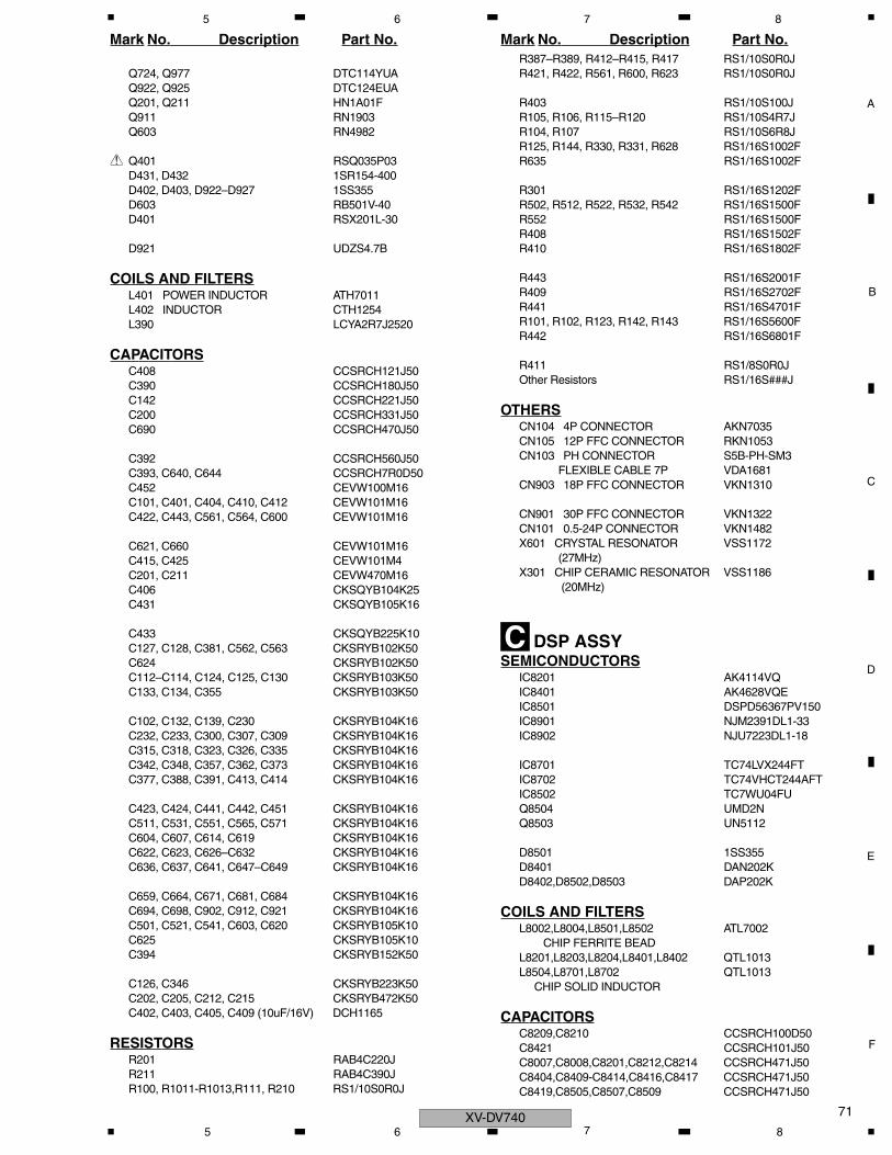
C
D
F
A
B
E
71
5 6 7 8
Q724, Q977 DTC114YUAQ922, Q925 DTC124EUAQ201, Q211 HN1A01FQ911 RN1903Q603 RN4982
> Q401 RSQ035P03D431, D432 1SR154-400D402, D403, D922–D927 1SS355D603 RB501V-40D401 RSX201L-30
D921 UDZS4.7B
COILS AND FILTERSL401 POWER INDUCTOR ATH7011L402 INDUCTOR CTH1254L390 LCYA2R7J2520
CAPACITORSC408 CCSRCH121J50C390 CCSRCH180J50C142 CCSRCH221J50C200 CCSRCH331J50C690 CCSRCH470J50
C392 CCSRCH560J50C393, C640, C644 CCSRCH7R0D50C452 CEVW100M16C101, C401, C404, C410, C412 CEVW101M16C422, C443, C561, C564, C600 CEVW101M16
C621, C660 CEVW101M16C415, C425 CEVW101M4C201, C211 CEVW470M16C406 CKSQYB104K25C431 CKSQYB105K16
C433 CKSQYB225K10C127, C128, C381, C562, C563 CKSRYB102K50C624 CKSRYB102K50C112–C114, C124, C125, C130 CKSRYB103K50C133, C134, C355 CKSRYB103K50
C102, C132, C139, C230 CKSRYB104K16C232, C233, C300, C307, C309 CKSRYB104K16C315, C318, C323, C326, C335 CKSRYB104K16C342, C348, C357, C362, C373 CKSRYB104K16C377, C388, C391, C413, C414 CKSRYB104K16
C423, C424, C441, C442, C451 CKSRYB104K16C511, C531, C551, C565, C571 CKSRYB104K16C604, C607, C614, C619 CKSRYB104K16C622, C623, C626–C632 CKSRYB104K16C636, C637, C641, C647–C649 CKSRYB104K16
C659, C664, C671, C681, C684 CKSRYB104K16C694, C698, C902, C912, C921 CKSRYB104K16C501, C521, C541, C603, C620 CKSRYB105K10C625 CKSRYB105K10C394 CKSRYB152K50
C126, C346 CKSRYB223K50C202, C205, C212, C215 CKSRYB472K50C402, C403, C405, C409 (10uF/16V) DCH1165
RESISTORSR201 RAB4C220JR211 RAB4C390JR100, R1011-R1013,R111, R210 RS1/10S0R0J
Mark No. Description Part No.R387–R389, R412–R415, R417 RS1/10S0R0JR421, R422, R561, R600, R623 RS1/10S0R0J
R403 RS1/10S100JR105, R106, R115–R120 RS1/10S4R7JR104, R107 RS1/10S6R8JR125, R144, R330, R331, R628 RS1/16S1002FR635 RS1/16S1002F
R301 RS1/16S1202FR502, R512, R522, R532, R542 RS1/16S1500FR552 RS1/16S1500FR408 RS1/16S1502FR410 RS1/16S1802F
R443 RS1/16S2001FR409 RS1/16S2702FR441 RS1/16S4701FR101, R102, R123, R142, R143 RS1/16S5600FR442 RS1/16S6801F
R411 RS1/8S0R0JOther Resistors RS1/16S###J
OTHERSCN104 4P CONNECTOR AKN7035CN105 12P FFC CONNECTOR RKN1053CN103 PH CONNECTOR S5B-PH-SM3 FLEXIBLE CABLE 7P VDA1681CN903 18P FFC CONNECTOR VKN1310
CN901 30P FFC CONNECTOR VKN1322CN101 0.5-24P CONNECTOR VKN1482X601 CRYSTAL RESONATOR VSS1172 (27MHz)X301 CHIP CERAMIC RESONATOR VSS1186 (20MHz)
CDSP ASSYSEMICONDUCTORS
IC8201 AK4114VQIC8401 AK4628VQEIC8501 DSPD56367PV150IC8901 NJM2391DL1-33IC8902 NJU7223DL1-18
IC8701 TC74LVX244FTIC8702 TC74VHCT244AFTIC8502 TC7WU04FUQ8504 UMD2NQ8503 UN5112
D8501 1SS355D8401 DAN202KD8402,D8502,D8503 DAP202K
COILS AND FILTERSL8002,L8004,L8501,L8502 ATL7002 CHIP FERRITE BEADL8201,L8203,L8204,L8401,L8402 QTL1013L8504,L8701,L8702 QTL1013 CHIP SOLID INDUCTOR
CAPACITORSC8209,C8210 CCSRCH100D50C8421 CCSRCH101J50C8007,C8008,C8201,C8212,C8214 CCSRCH471J50C8404,C8409-C8414,C8416,C8417 CCSRCH471J50C8419,C8505,C8507,C8509 CCSRCH471J50
Mark No. Description Part No.
XV-DV7405 6 7 8
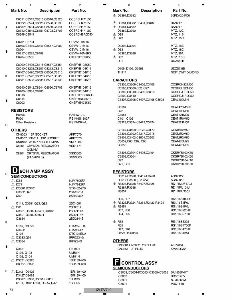
C
D
F
A
B
E
XV-DV74072
1 2 3 4
C8511,C8512,C8515,C8518,C8520 CCSRCH471J50C8522,C8524,C8526,C8528,C8530 CCSRCH471J50C8532,C8534,C8536,C8539,C8541 CCSRCH471J50C8543,C8545,C8551,C8703,C8706 CCSRCH471J50C8548,C8549 CCSRCH8R0D50
C8701,C8704 CEVW100M16C8406,C8415,C8546,C8547,C8902 CEVW101M16C8904 CEVW101M16C8217,C8225,C8408 CEVW470M6R3C8204,C8555 CKSRYB102K50
C8009,C8405,C8418,C8517,C8554 CKSRYB103K50C8010,C8202,C8207,C8213,C8215 CKSRYB104K16C8407,C8420,C8422,C8504,C8513 CKSRYB104K16C8521,C8523,C8525,C8527,C8529 CKSRYB104K16C8531,C8533,C8535,C8537,C8538 CKSRYB104K16
C8540,C8542,C8544,C8550,C8702 CKSRYB104K16C8705,C8901,C8903 CKSRYB104K16C8516 CKSRYB105K6R3C8514 CKSRYB333K16C8203 CKSRYB473K50
RESISTORSR8506 RAB4C101JR8201 RS1/16S1802FOther Resistors RS1/16S###J
OTHERSCN8003 13P SOCKET AKP7070CN8007,CN8011 19P SOCKET AKP7073KN8102 WRAPPING TERMINAL VNF1084X8501 CRYSTAL RESONATOR VSS1171 (20MHz)X8201 CRYSTAL RESONATOR XSS3003 (24.576MHz) XSS3003
D6CH AMP ASSYSEMICONDUCTORS> IC81 NJM7805FA> IC71 NJM7912FA> IC3301,IC3401 STK402-270
Q3382,Q43 2SA1576AQ62 2SB1237X
Q111, Q3381,Q63, Q92 2SC4081> Q61 2SD2012
Q3301,Q3302,Q3401,Q3402 2SD2114KQ3501,Q3502,Q3504 2SD2114KQ3654 2SD2144S
Q107, Q3653 DTA124EUAQ3652 DTA124TKQ106 DTC124EUA
> Q3383,Q91 IRFI9Z34G> Q3384 IRFIZ34G
Q3651 RN1901Q101, Q103 UMB1NQ102, Q104 UMH1N
> D3321-D3326 1SR139-400D3327,D3328 1SR139-400
> D3421-D3426 1SR139-400D3427,D3428 1SR139-400D3387,D3388,D3651-D3655 1SS133D101, D102, D104, D3657,D42 1SS355
Mark No. Description Part No.> D3391,D3392 30PDA20-FC6
> D3381,D3382,D3481,D3482 DAN217> D3581,D3582 DAN217
D3389,D3390 MTZJ10C> D98 MTZJ11B> D72 MTZJ15C
D3393,D3394 MTZJ18B> D63 MTZJ18C
D3385,D3386 MTZJ36A> D82 MTZJ7.5C
D91 UDZS18B
D105, D106, D3658 UDZS7.5BTH111 NCP18WF104J03RB
CAPACITORSC3305,C3306,C3405,C3406 CCSRCH221J50C3505,C3506,C62, C97 CCSRCH221J50C3309,C3310,C3409,C3410 CCSRCJ3R0C50C3509,C3510 CCSRCJ3R0C50C3307,C3308,C3407,C3408,C3508 CEAL100M16
C3507 CEAL470M6R3C72 CEAT100M50C3651 CEAT101M25C101, C102 CEAT1R0M50C3323,C3324,C3423,C3424 CEAT221M50
C3167,C3168,C3178,C3179 CEAT2R2M50C3301,C3302,C3317,C3318 CEAT2R2M50C3401,C3402,C3501,C3502 CEAT2R2M50C3652,C63, C82, C98 CEAT470M25C3653 CEAT470M35
C3303,C3304,C3403,C3404 CKSRYB102K50C3503,C3504 CKSRYB102K50C92 CKSRYB104K16C71, C81 CKSRYB473K50
RESISTORSR3317-R3320,R3417-R3420 ACN7122R3517-R3520 (0.22/2W) ACN7122
> R3327,R3328,R3427,R3428 RD1/4MUF470JR3387,R3388 RD1/4PU101JR3657 RD1/4PU330J
R96, R97 RS1/16S1002F> R3323,R3324,R3351,R3423,R3424 RS1/16S1R0J> R3451 RS1/16S1R0J
R67, R68 RS1/16S2201FR94, R95 RS1/16S2701F
> R62 RS1/16S330JR65 RS1/16S4700FR47, R48 RS1/16S4701FOther Resistors RS1/16S###J
OTHERSCN3001,CN3002 23P PLUG AKP7064CN3651 2P PLUG KM200SA2
FCONTROL ASSYSEMICONDUCTORS
IC3003,IC3051-IC3053,IC3055-IC3058 BA4558F-HTIC3062 BD3814FVIC3901 NJM4565MIC5501 PDC114B
Mark No. Description Part No.
1 2 3 4
C
D
F
A
B
E
73
5 6 7 8
IC3001 TC4052BFN
IC3059 TC4066BFNQ5576,Q5577 2SA1037KQ3906 2SA1576AQ3005,Q3006,Q3009,Q3010,Q5501 2SC4081Q5572 2SC4081
Q5711 2SD1858XQ3001,Q3002 2SD2114KQ3003,Q3061,Q3069,Q3071 DTA124EUAQ3060,Q3070,Q5575,Q5578,Q5579 DTC124EUAQ5571 DTC143EUA
Q5595 RN2901Q3004 UMB1ND3901 DAP202KD5570,D5571,D5573,D5575 MA111D5595,D5596,D5712 MA111
D5711 UDZS10BD3003,D3004 UDZS6.2BD3052,D3053 UDZS6.8B
COILS AND FILTERSL5571 LFEA220JL8881-L8884 QTL1013 CHIP SOLID INDUCTORF8604 CHIP SOLID INDUCTOR VTF1096
CAPACITORSC5575 (0.047F/5.5V) ACH1246C3111,C3112,C3130,C3145,C3146 CCSRCH100D50C3131-C3133,C3913,C3914 CCSRCH101J50C5510,C5511,C5577,C5722,C5723 CCSRCH101J50C3001-C3008 CCSRCH221J50
C3053,C3054 CCSRCH331J50C3041,C3168,C3909,C3910 CCSRCH470J50C3059,C3060 CCSRCH680J50C3009,C3010,C3055,C3056 CCSRCH821J50C3077,C3078,C3089 CCSRCH821J50
C3134,C3189,C3190,C3906,C5711 CEAL100M16C3149,C3150 CEAL470M16C3017-C3020,C3037,C3038 CEAT100M50C3079,C3080,C3085,C3086 CEAT100M50C3093,C3094,C3173,C3174 CEAT100M50
C3917,C3918,C5576 CEAT100M50C5572 CEAT101M10C5578 CEAT1R0M50C3113,C3114 CEAT221M10C3027,C3028,C3911,C3912 CEAT470M16
C3919,C3920,C8610 CEAT470M16C3051,C3052,C3061,C3062 CEJQ100M16C3069,C3070 CEJQ100M16C3035,C3036 CEJQ100M35C5595,C5596 CEJQ220M25
C3065,C3066 CEJQ470M16C5504,C5789,C5793,C5795 CKSRYB102K50C3025,C3026,C3033,C3034 CKSRYB103K50C3067,C3068,C3083,C3084 CKSRYB103K50C3091,C3092,C3115,C3116 CKSRYB103K50
C3147,C3148,C3159,C3160 CKSRYB103K50C3169-C3172,C5506,C5508,C5571 CKSRYB103K50C5573,C5580,C5794,C5798,C5799 CKSRYB103K50C3121-C3124,C3180,C3182,C3186 CKSRYB104K16
Mark No. Description Part No.C5513-C5516,C5574,C5791,C8609 CKSRYB104K16
C8611 CKSRYB104K16C3176 CKSRYB123K50C3071,C3072,C3075,C3076,C3087 CKSRYB152K50C3097,C3138,C3155,C3156 CKSRYB152K50C3183 CKSRYB183K25
C3141,C3142 CKSRYB223K50C3181 CKSRYB273K16C3161,C3162 CKSRYB332K50C3165 CKSRYB393K16C3125,C3126 CKSRYB472K50
C3177,C3193,C3194 CKSRYB473K25C3179 CKSRYB563K16C3090 CKSRYB682K50C3195 CKSRYB683K16
RESISTORSR3118,R3119 RD1/2VM151JR3041,R3042 RS1/10S182JOther Resistors RS1/16S###J
OTHERSCN3902 5P FFC CONNECTOR 52045-0545CN5701 11P FFC CONNECTOR 52045-1145CN5611 15P FFC CONNECTOR 52045-1545JA3001 6P PIN JACK AKB7050
CN5613 11P PLUG AKP7058CN5612,CN5620 19P PLUG AKP7062CN5501,CN5502 23P PLUG AKP7064X5501 CERAMIC RESONATOR ASS7034 (10MHz)
JA8602 OPTICAL INPUT JACK TORX179PLKN5501,KN5791 TERMINAL VNF1084JA8803 MINI JACK(4P) /W SW XKN3015
GTRADE 3 ASSYOTHERS
CN5615 13P PLUG AKP7059CN5614,CN5618 19P PLUG AKP7062CN5617 11P SOCKET AKP7069CN5616,CN5619 19P SOCKET AKP7073
HTRADE 2 ASSYSEMICONDUCTORS
Q114 2SD2114KQ115 DTA124EUA
RESISTORSAll Resistors RS1/16S###J
OTHERSCN5511,CN5512,CN5521,CN5522 AKP7075 23P SOCKET
IHP ASSYSEMICONDUCTORS
Q3903 DTA124EUAQ3901,Q3921 XP4506
Mark No. Description Part No.
XV-DV7405 6 7 8
C
D
F
A
B
E
XV-DV74074
1 2 3 4
COILS AND FILTERSL3901,L3902 CHIP BEAD CTF1399
CAPACITORSC3901,C3902 CKSRYB102K50C3905 CKSRYB103K50C3925 CKSRYB104K16C3903,C3904 CKSRYB473K25
RESISTORSR3901,R3902,R3911,R3912 RS1/10S680JR3961-R3964 RS1/10S680JOther Resistors RS1/16S###J
OTHERSCN3901 5P FFC CONNECTOR 52044-05453901 MINI JACK AKN7003 PCB BINDER VEF1040
JPOWER ASSYSEMICONDUCTORS> IC61 NJM7812FA> IC51 NJM78M56FA> Q32 2SB1565
Q3601,Q3602,Q3611,Q3612 2SC4081Q3621,Q3622,Q3631,Q3637,Q3638 2SC4081
Q3642,Q3644,Q52 2SC4081Q3641,Q51 2SD1858XQ3635,Q3639 DTA124EUAQ3645 DTA143EUAQ3636,Q3640 DTC124EUA
Q3633 RN1901Q3632 UMB1ND35, D3632-D3634,D52 1SS133
> D11, D21, D22 D5SBA20D3635 DAN202K
D3644,D53 DAN217D3603,D3613,D3623 DAP202K
> D51 DF06SAD103, D3601,D3602,D3611,D3612 MA111D3621,D3622,D3636,D3637 MA111
D3641-D3643 MA111D33, D34 MTZJ16BD3631 MTZJ5.1AD36 MTZJ6.8B
> D31, D32 S5688G
D55 UDZS20B
COILS AND FILTERSL3361,L3362,L3461,L3462,L3561 ATH-059L3661 AF CHOKE COIL ATH-059L3701 CHIP BEAD VTL1075L8821 CHIP BEAD VTL1086
> L1 LINE FILTER XTF3004
TRANSFORMERS> T2 ATT7079
SWITCHES AND RELAYSRY3641-RY3643 ASR7017
> RY1 XSR3008
CAPACITORS
Mark No. Description Part No.> C1, C2 (0.022/AC275V) ACE7022
C25 ACH7183C3633 CEAT100M50C52 CEAT102M16C33, C34, C67 CEAT220M50
C32 CEAT221M63C3631 CEAT2R2M2AC54 CEAT470M16C3632 CEAT471M6R3C35 CEJQ100M50
C53 CKSRYB103K50C3361-C3364,C3461-C3464,C3561 CKSRYB223K50C3563,C3661,C3663 CKSRYB223K50C3365-C3368,C3465-C3468,C3565 CKSRYB473K50C3567,C3665,C3667,C56–C58 CKSRYB473K50
C66 CKSRYB473K50C22, C26, C27 CQMA472J50C3369,C3370,C3469,C3470,C3569 XCG3008C3669 (0.01pF/100V) XCG3008C8821,C8831 (1000uF/6.3V) XCH3017
C8885 XCH3021C23, C24 (5600uF/35V) XCH3023C15, C16 (2200uF/63V) XCH3024
RESISTORSR3607,R3608,R3617,R3618 ACN7112R3627,R3628 (0.1/ 2W) ACN7112R1 (2.2M/ 1/2W) RCN1080R21 RD1/2PMF100JR3361,R3362,R3461,R3462,R3561 RD1/2PMF101J
R3661 RD1/2PMF101JR31 RD1/2PMF332JR36, R37 RD1/4PU101JR3635 RD1/4PU332JR3631,R3632 RD1/4PU333J
R35 RD1/4PU472JR3365-R3368,R3465-R3468 RS1/10S220JR3565,R3566,R3665,R3667 RS1/10S220JR8831,R8832,R8841,R8842 RS1/16S1500FR8821 RS1/16S75R0F
Other Resistors RS1/16S###J
OTHERSCN8807 5P FFC CONNECTOR 52045-0545CN3031,CN3032,CN5531,CN5532 AKP7064 23P PLUGCN8802 4P MINI DIN SOCKET AKP7179H1–H4 FUSE CLIP AKR7001CN11 10P VH CONNECTOR B10P-VH
> CN2 2P VH CONNECTOR B2P3-VH SCREW BBZ30P080FTC PCB BINDER VEF1040JA8803 1P PIN JACK VKB1122CN8801 18P FFC CONNECTOR VKN1249CN5102 30P FFC CONNECTOR VKN1261CN8003 7P FFC CONNECTOR VKN1267KN1, KN2 WRAPPING TERMINAL VNF1084JA3301 6CH SPEAKER JACK XKE3021
> AN1 AC INLET 1P XKP3042 D. HEAT SINK XNH3030
KTRADE 1 ASSY
Mark No. Description Part No.
1 2 3 4
C
D
F
A
B
E
75
5 6 7 8
SEMICONDUCTORS> IC25 (7A) AEK7021
RESISTORSAll Resistors RS1/16S###J
OTHERSCN3011,CN3012,CN3021,CN3022 AKP7075 23P SOCKET
LVIDEO ASSYCOILS AND FILTERS
L8951 CHIP BEADS VTL1086L8961,L8971 CHIP BEADS VTL1089
CAPACITORSC8952,C8962,C8972 CCSRCH470J50C8951 CEAT102M6R3C8961,C8971 CEAT471M6R3
RESISTORSR8953,R8963,R8973 RS1/16S75R0F
OTHERSCN8001 5P FFC CONNECTOR 52045-0545JA8951 3P PIN JACK VKB1150
MDISPLAY ASSYSEMICONDUCTORS
IC5601 PT6302LQ-003Q5691 2SC4081Q5692,Q5693 DTC143EUAD5932 E1L33-AB0A2-02D5662 MTZJ36B
D5931 SLR-56MCD5933 UDZS6.8B
COILS AND FILTERSL5563 LAU100JL5562 LAU220J
SWITCHES AND RELAYSS5921-S5927 VSG1024
CAPACITORSC5674 CCSRCH470J50C5661,C5663 CCSRCH471J50C5564 CEAL101M6R3C5679,C5680 CEAL1R0M50C5678 CEAL220M35
C5953 CEAL470M16C5671-C5673 CKSRYB102K50C5677,C5681 CKSRYB103K50C5562,C5563,C5665,C5666,C5675 CKSRYB223K50C5952 CKSRYB223K50
C5676 CHIP VARISTOR VCX1001
RESISTORSAll Resistors RS1/16S###J
OTHERSCN5601 15P FFC CONNECTOR 52044-1545
Mark No. Description Part No.5951 REMOTE RECEIVER UNIT GP1UM27XK FL HOLDER VNF1122V5601 FL TUBE XAV3021
FM/AM TUNER UNITFM/AM TUNER UNIT has no service part.
Mark No. Description Part No.
XV-DV7405 6 7 8
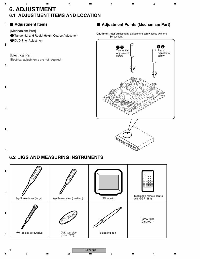
C
D
F
A
B
E
XV-DV74076
1 2 3 4
6. ADJUSTMENT6.1 ADJUSTMENT ITEMS AND LOCATION
6.2 JIGS AND MEASURING INSTRUMENTS
1
1 2
2
Tangentialadjustmentscrew
1 2Radialadjustmentscrew
Adjustment Items
[Mechanism Part]
[Electrical Part]
Tangential and Radial Height Coarse Adjustment
DVD Jitter Adjustment
Electrical adjustments are not required.
Adjustment Points (Mechanism Part)
Cautions: After adjustment, adjustment screw locks with the Screw tight.
Screwdriver (large) TV monitor
Precise screwdriver DVD test disc(GGV1025)
Test mode remote controlunit (GGF1381)
Screw tight(GYL1001)
Screwdriver (medium)
Soldering iron
1 2 3 4
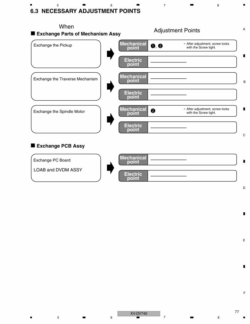
C
D
F
A
B
E
77
5 6 7 8
6.3 NECESSARY ADJUSTMENT POINTS
∗ After adjustment, screw locks with the Screw tight.
∗ After adjustment, screw locks with the Screw tight.
~, Ÿ
Ÿ
Mechanicalpoint
Electricpoint
Mechanicalpoint
Electricpoint
Mechanicalpoint
Electricpoint
Mechanicalpoint
Electricpoint
LOAB and DVDM ASSY
Exchange Parts of Mechanism Assy
Exchange PCB Assy
WhenAdjustment Points
Exchange the Pickup
Exchange the Traverse Mechanism
Exchange the Spindle Motor
Exchange PC Board
XV-DV7405 6 7 8
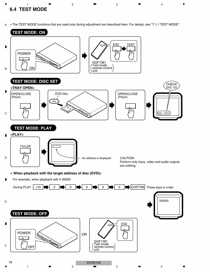
C
D
F
A
B
E
XV-DV74078
1 2 3 4
6.4 TEST MODE
TEST MODE: ON
TEST MODE: DISC SET
DSC - &&&
GGF1381Test moderemote controlunit
GGF1381Test moderemote controlunit
<TRAY OPEN>
OPEN/CLOSE(Player)
OPEN/CLOSE(Player)
TEST MODE: PLAY
TEST MODE: OFF
An address is displayed
For example, when playback with # 30000
During PLAY Press keys in order
OR
ESC
030000
<PLAY>
< When playback with the target address of disc (DVD)>
TV/LDP
+10 3 0 0 0 0 CHP/TIM
ESC TEST
CHECKDVD, CD
CAUTION:Perform only trace, video and audio outputs are nothing.
• The TEST MODE functions that are used only during adjustment are described here. For details, see "7.1.1 TEST MODE".
DVD disc
POWER
ON
POWER
OFF
1 2 3 4
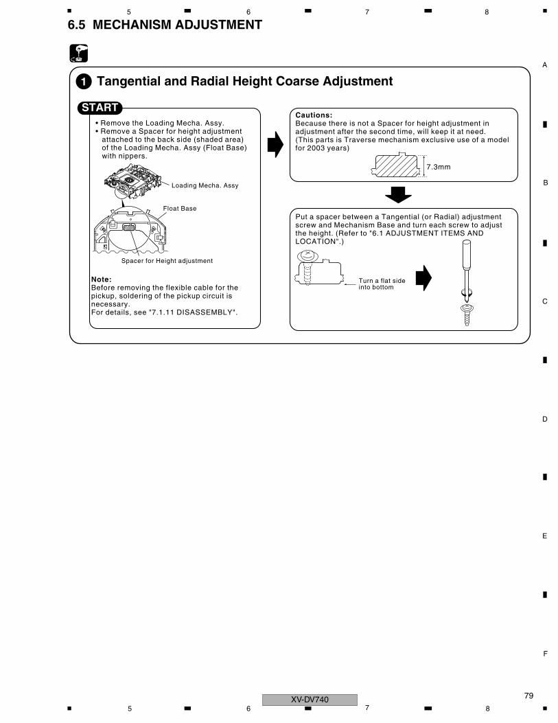
C
D
F
A
B
E
79
5 6 7 8
6.5 MECHANISM ADJUSTMENT
• Remove the Loading Mecha. Assy.• Remove a Spacer for height adjustment
attached to the back side (shaded area)of the Loading Mecha. Assy (Float Base) with nippers.
Cautions:Because there is not a Spacer for height adjustment in adjustment after the second time, will keep it at need.(This parts is Traverse mechanism exclusive use of a modelfor 2003 years)
Put a spacer between a Tangential (or Radial) adjustment screw and Mechanism Base and turn each screw to adjustthe height. (Refer to "6.1 ADJUSTMENT ITEMS AND LOCATION".)
START
Tangential and Radial Height Coarse Adjustment1
Loading Mecha. Assy
7.3mm
Turn a flat sideinto bottom
Spacer for Height adjustment
Float Base
Note:Before removing the flexible cable for the pickup, soldering of the pickup circuit is necessary.For details, see "7.1.11 DISASSEMBLY".
XV-DV7405 6 7 8
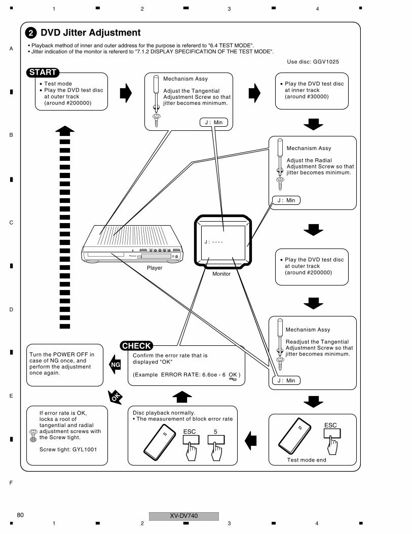
C
D
F
A
B
E
XV-DV74080
1 2 3 4
PHONES
6 DVD/CD0 OPEN/CLOSE FM/AM VOL.ñ DOWN UP +7 STANDBY/ON
PlayerMonitor
• Test mode• Play the DVD test disc
at outer track(around #200000)
• Play the DVD test discat inner track(around #30000)
• Play the DVD test discat outer track(around #200000)
Mechanism Assy
Adjust the TangentialAdjustment Screw so thatjitter becomes minimum.
Mechanism Assy
Readjust the TangentialAdjustment Screw so thatjitter becomes minimum.
Mechanism Assy
Adjust the RadialAdjustment Screw so thatjitter becomes minimum.
Use disc: GGV1025
START
DVD Jitter Adjustment2
J : - - - -
J : Min
J : Min
Test mode end
J : Min
ESC
Disc playback normally.• The measurement of block error rate
If error rate is OK, locks a root of tangential and radial adjustment screws withthe Screw tight.
Screw tight: GYL1001
Turn the POWER OFF in case of NG once, and perform the adjustment once again.
Confirm the error rate that is displayed "OK"
(Example ERROR RATE: 6.6oe - 6 OK )
5ESC
CHECK
NG
OK
• Playback method of inner and outer address for the purpose is refererd to "6.4 TEST MODE".• Jitter indication of the monitor is refererd to "7.1.2 DISPLAY SPECIFICATION OF THE TEST MODE".
Mechanism Assy
Readjust the TangentialAdjustment Screw so thatjitter becomes minimum.
J : Min
1 2 3 4
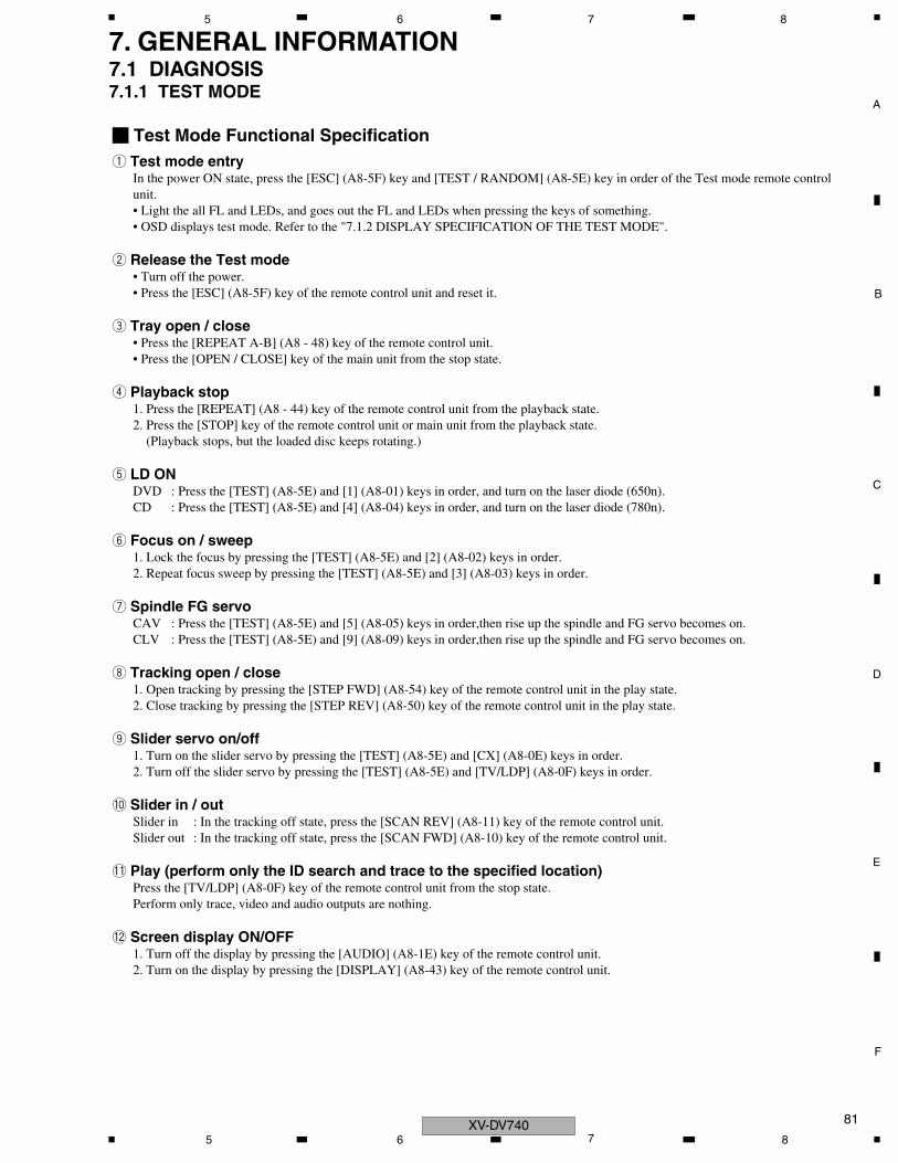
C
D
F
A
B
E
81
5 6 7 8
7. GENERAL INFORMATION7.1 DIAGNOSIS7.1.1 TEST MODE
Test Mode Functional Specification1 Test mode entry
In the power ON state, press the [ESC] (A8-5F) key and [TEST / RANDOM] (A8-5E) key in order of the Test mode remote control unit. • Light the all FL and LEDs, and goes out the FL and LEDs when pressing the keys of something. • OSD displays test mode. Refer to the "7.1.2 DISPLAY SPECIFICATION OF THE TEST MODE".
2 Release the Test mode• Turn off the power.• Press the [ESC] (A8-5F) key of the remote control unit and reset it.
3 Tray open / close• Press the [REPEAT A-B] (A8 - 48) key of the remote control unit.• Press the [OPEN / CLOSE] key of the main unit from the stop state.
4 Playback stop1. Press the [REPEAT] (A8 - 44) key of the remote control unit from the playback state.2. Press the [STOP] key of the remote control unit or main unit from the playback state. (Playback stops, but the loaded disc keeps rotating.)
5 LD ONDVD : Press the [TEST] (A8-5E) and [1] (A8-01) keys in order, and turn on the laser diode (650n).CD : Press the [TEST] (A8-5E) and [4] (A8-04) keys in order, and turn on the laser diode (780n).
6 Focus on / sweep1. Lock the focus by pressing the [TEST] (A8-5E) and [2] (A8-02) keys in order.2. Repeat focus sweep by pressing the [TEST] (A8-5E) and [3] (A8-03) keys in order.
7 Spindle FG servoCAV : Press the [TEST] (A8-5E) and [5] (A8-05) keys in order,then rise up the spindle and FG servo becomes on.CLV : Press the [TEST] (A8-5E) and [9] (A8-09) keys in order,then rise up the spindle and FG servo becomes on.
8 Tracking open / close1. Open tracking by pressing the [STEP FWD] (A8-54) key of the remote control unit in the play state.2. Close tracking by pressing the [STEP REV] (A8-50) key of the remote control unit in the play state.
9 Slider servo on/off1. Turn on the slider servo by pressing the [TEST] (A8-5E) and [CX] (A8-0E) keys in order.2. Turn off the slider servo by pressing the [TEST] (A8-5E) and [TV/LDP] (A8-0F) keys in order.
0 Slider in / outSlider in : In the tracking off state, press the [SCAN REV] (A8-11) key of the remote control unit.Slider out : In the tracking off state, press the [SCAN FWD] (A8-10) key of the remote control unit.
- Play (perform only the ID search and trace to the specified location)Press the [TV/LDP] (A8-0F) key of the remote control unit from the stop state.Perform only trace, video and audio outputs are nothing.
= Screen display ON/OFF1. Turn off the display by pressing the [AUDIO] (A8-1E) key of the remote control unit.2. Turn on the display by pressing the [DISPLAY] (A8-43) key of the remote control unit.
XV-DV7405 6 7 8
C
D
F
A
B
E
XV-DV74082
1 2 3 4
~ Search1. Search address input entry• It becomes the address input mode when pressing the [+10] (A8-1F) key. (Most significant digit of an address displays "<".)• In this time, display the last address as the initial state.
2. Search address input• Press the [0] to [9] (A8-00 to 09) keys of the remote control unit. In the DVD, set an address with hexadecimal.• In the address input mode, turn to the hexadecimal input by pressing the [PROGRAM] (A8-4C) key (display a "∗" mark), and [1] to [6] keys are each input as A to F.• Hexadecimal input and decimal input can switch with toggle. • In case of CD, perform only the absolute time search.
3. Search execution• Press the [CHP/TM] (A8-13) key of the remote control unit.• After the search, perform only trace and video and audio outputs are nothing.
4. Release the Search address input• Clear the address by pressing the [CLEAR] (A8-45) key. Release the address input mode when pressing the [CLEAR] key once again.
1 2 3 4
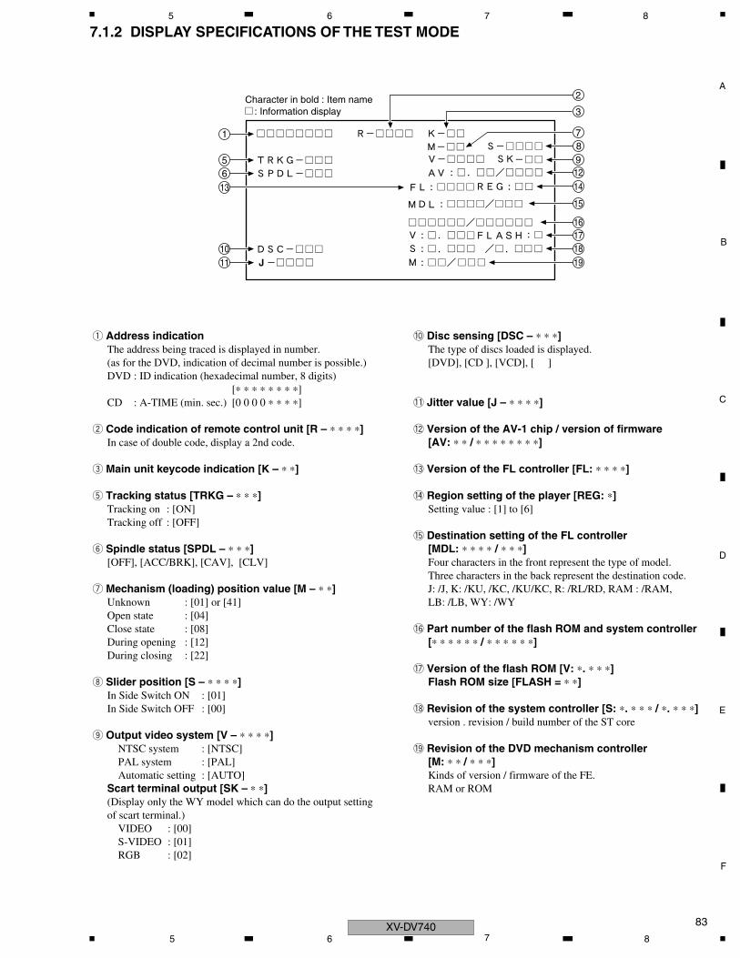
C
D
F
A
B
E
83
5 6 7 8
7.1.2 DISPLAY SPECIFICATIONS OF THE TEST MODE
Character in bold : Item name: Information display
1
56
10
13
11
89
3
2
12
171819
16
14
15
1 Address indicationThe address being traced is displayed in number. (as for the DVD, indication of decimal number is possible.)DVD : ID indication (hexadecimal number, 8 digits)
[∗ ∗ ∗ ∗ ∗ ∗ ∗ ∗]CD : A-TIME (min. sec.) [0 0 0 0 ∗ ∗ ∗ ∗]
2 Code indication of remote control unit [R – ∗ ∗ ∗ ∗]In case of double code, display a 2nd code.
3 Main unit keycode indication [K – ∗ ∗]
5 Tracking status [TRKG – ∗ ∗ ∗]Tracking on : [ON]Tracking off : [OFF]
6 Spindle status [SPDL – ∗ ∗ ∗][OFF], [ACC/BRK], [CAV], [CLV]
7 Mechanism (loading) position value [M – ∗ ∗]Unknown : [01] or [41]Open state : [04]Close state : [08]During opening : [12]During closing : [22]
8 Slider position [S – ∗ ∗ ∗ ∗]In Side Switch ON : [01]In Side Switch OFF : [00]
9 Output video system [V – ∗ ∗ ∗ ∗]NTSC system : [NTSC]PAL system : [PAL]Automatic setting : [AUTO]
Scart terminal output [SK – ∗ ∗] (Display only the WY model which can do the output settingof scart terminal.)
VIDEO : [00] S-VIDEO : [01]RGB : [02]
0 Disc sensing [DSC – ∗ ∗ ∗]The type of discs loaded is displayed.[DVD], [CD ], [VCD], [ ]
- Jitter value [J – ∗ ∗ ∗ ∗]
= Version of the AV-1 chip / version of firmware[AV: ∗ ∗ / ∗ ∗ ∗ ∗ ∗ ∗ ∗ ∗]
~ Version of the FL controller [FL: ∗ ∗ ∗ ∗]
! Region setting of the player [REG: ∗]Setting value : [1] to [6]
@ Destination setting of the FL controller[MDL: ∗ ∗ ∗ ∗ / ∗ ∗ ∗]Four characters in the front represent the type of model.Three characters in the back represent the destination code.J: /J, K: /KU, /KC, /KU/KC, R: /RL/RD, RAM : /RAM, LB: /LB, WY: /WY
# Part number of the flash ROM and system controller[∗ ∗ ∗ ∗ ∗ ∗ / ∗ ∗ ∗ ∗ ∗ ∗]
$ Version of the flash ROM [V: ∗. ∗ ∗ ∗]Flash ROM size [FLASH = ∗ ∗]
% Revision of the system controller [S: ∗. ∗ ∗ ∗ / ∗. ∗ ∗ ∗]version . revision / build number of the ST core
^ Revision of the DVD mechanism controller[M: ∗ ∗ / ∗ ∗ ∗]Kinds of version / firmware of the FE.RAM or ROM
7
XV-DV7405 6 7 8
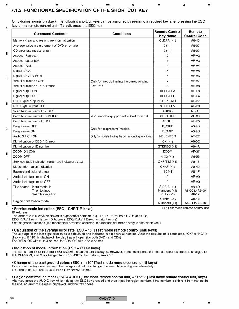
C
D
F
A
B
E
XV-DV74084
1 2 3 4
7.1.3 FUNCTIONAL SPECIFICATION OF THE SHORTCUT KEY
• Service mode indication (ESC + CHP/TIM keys)ID AddressThe error rate is always displayed in exponential notation, e.g., ∗.∗ ∗ e - ∗, for both DVDs and CDs.EDC/ID/AV 1 error history (ID Address, EDC/ID/AV 1 Error, last eight errors)Self-diagnosis functions (If a mechanical error has occurred, the mechanical-error history is also displayed.)
• Calculation of the average error rate (ESC + "5" [Test mode remote control unit] keys)The average of the last eight error rates is calculated and indicated in exponential notation. After the calculation is completed, "OK" or "NG" is displayed. If "NG" is displayed, the disc tray will open (for both DVDs and CDs)For DVDs: OK with 5.0e-4 or less, for CDs: OK with 7.6e-3 or less
• Indication of model information (ESC + CHAP keys)The items from 12 to 19 of the TEST MODE Indications are displayed. However, in the indications, S in the standard test mode is changed to B.E VERSION, and M is changed to F.E VERSION. For details, see 7.1.4.
• Change of the background colors (ESC + "+10" [Test mode remote control unit] keys)Every time the keys are pressed, the background color is changed between blue and green alternately.(The green background is used in SETUP NAVIGATOR.)
• Region confirmation mode (ESC + AUDIO [Test mode remote control unit] + "1"-"8" [Test mode remote control unit] keys)After you press the AUDIO key while holding the ESC key pressed and then input the region number, if the number is different from that set in the unit, an error message is displayed, and the tray opens.
Command Contents ConditionsRemote Control
Key NameRemote
Control CodeMemory clear and resion / revision indication CLEAR (∗1) A8-45
Average value measurement of DVD error rate 5 (∗1) A8-05
CD error rate measurement 5 (∗1) A8-05
Aspect : Pan scan 2 AF-A2
Aspect : Letter box 3 AF-A3
Aspect : Wide 4 AF-A4
Digital : AC3 5 AF-A5
Digital : AC-3 > PCM 6 AF-A6
Virtual surround : OFF Only for models having the corresponding functions
7 AF-A7
Virtual surround : TruSurround 8 AF-A8
Digital output ON REPEAT A AF-E8
Digital output OFF REPEAT B AF-E4
DTS Digital output ON STEP FWD AF-B7
DTS Digtal output OFF STEP REV AF-B8
Scart terminal output : VIDEO
WY, models equipped with Scart terminal
AUDIO AF-BE
Scart terminal output : S-VIDEO SUBTITLE AF-36
Scart terminal output : RGB ANGLE AF-B5
Progressive OFFOnly for progressive models
R_SKIP A3-9D
Progressive ON F_SKIP A3-9C
Audio 5.1 CH ON Only for models having the corresponding functions KD_ENTER AF-EF
FL indication of EDC / ID error CX (∗1) A8-0E
FL indication of ID number STEREO (∗1) A8-4A
ZOOM ON (X4) ZOOM AF-37
ZOOM OFF < X3 (∗1) A8-59
Service mode indication (error rate indication, etc.) CHP/TIM (∗1) A8-13
Model information indication CHAP (∗1) A8-40
Background color change +10 (∗1) A8-1F
Audio last stage mute ON 9 AF-A9
Audio last stage mute OFF 0 AF-A0
Title search Input mode INTitle No. inputSearch execution
SIDE A (∗1)Numbers (∗1)
PLAY (∗1)
A8-4DA8-00 to A8-09
A8-17
Region confimation modeAUDIO (∗1)
Numbers (∗1)A8-1E
A8-01 to A8-08
Only during normal playback, the following shortcut keys can be assigned by pressing a required key after pressing the ESC key of the remote control unit. To quit, press the ESC key
∗1 : Test mode remote control unit
1 2 3 4
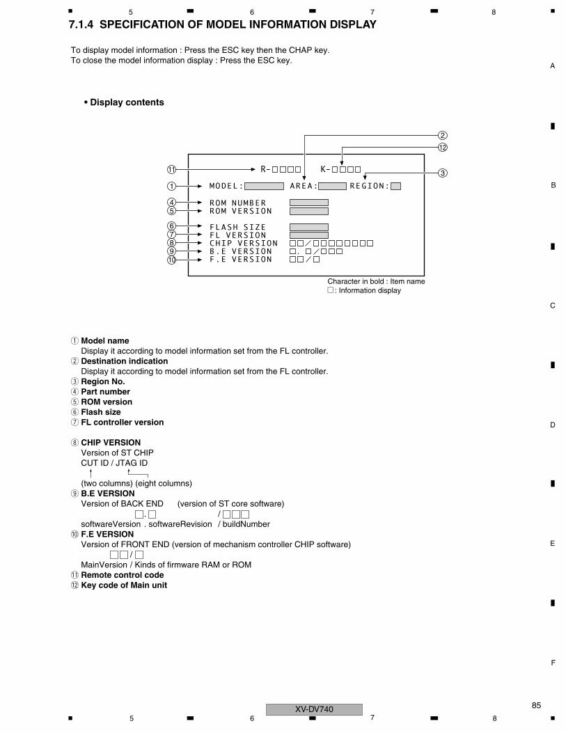
C
D
F
A
B
E
85
5 6 7 8
7.1.4 SPECIFICATION OF MODEL INFORMATION DISPLAY
• Display contents
Character in bold : Item name: Information display
1
2
12
3
45
678910
11
1 Model nameDisplay it according to model information set from the FL controller.
2 Destination indicationDisplay it according to model information set from the FL controller.
3 Region No.4 Part number5 ROM version6 Flash size7 FL controller version
8 CHIP VERSIONVersion of ST CHIPCUT ID / JTAG ID
(two columns) (eight columns)9 B.E VERSION
Version of BACK END (version of ST core software). /
softwareVersion . softwareRevision / buildNumber0 F.E VERSION
Version of FRONT END (version of mechanism controller CHIP software)/
MainVersion / Kinds of firmware RAM or ROM - Remote control code= Key code of Main unit
To display model information : Press the ESC key then the CHAP key.To close the model information display : Press the ESC key.
XV-DV7405 6 7 8
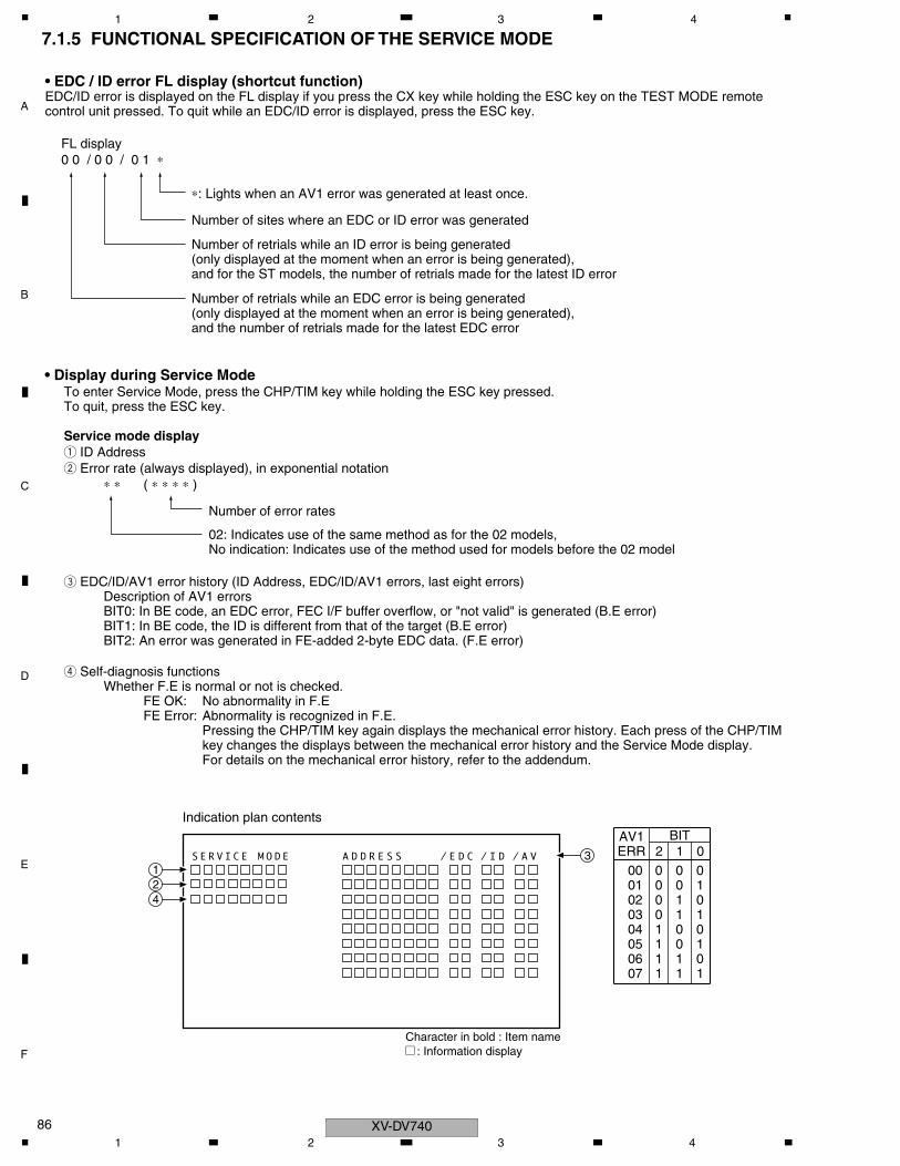
C
D
F
A
B
E
XV-DV74086
1 2 3 4
7.1.5 FUNCTIONAL SPECIFICATION OF THE SERVICE MODE
Indication plan contents
Character in bold : Item name: Information display
124
• EDC / ID error FL display (shortcut function)EDC/ID error is displayed on the FL display if you press the CX key while holding the ESC key on the TEST MODE remote control unit pressed. To quit while an EDC/ID error is displayed, press the ESC key.
FL display0 0 / 0 0 / 0 1 ∗
• Display during Service ModeTo enter Service Mode, press the CHP/TIM key while holding the ESC key pressed.To quit, press the ESC key.
Service mode display1 ID Address2 Error rate (always displayed), in exponential notation
∗ ∗ ( ∗ ∗ ∗ ∗ )
3 EDC/ID/AV1 error history (ID Address, EDC/ID/AV1 errors, last eight errors)Description of AV1 errorsBIT0: In BE code, an EDC error, FEC I/F buffer overflow, or "not valid" is generated (B.E error)BIT1: In BE code, the ID is different from that of the target (B.E error)BIT2: An error was generated in FE-added 2-byte EDC data. (F.E error)
4 Self-diagnosis functionsWhether F.E is normal or not is checked.
FE OK: No abnormality in F.EFE Error: Abnormality is recognized in F.E.
Pressing the CHP/TIM key again displays the mechanical error history. Each press of the CHP/TIM key changes the displays between the mechanical error history and the Service Mode display.For details on the mechanical error history, refer to the addendum.
Number of sites where an EDC or ID error was generated
∗: Lights when an AV1 error was generated at least once.
Number of retrials while an ID error is being generated (only displayed at the moment when an error is being generated), and for the ST models, the number of retrials made for the latest ID error
Number of retrials while an EDC error is being generated (only displayed at the moment when an error is being generated), and the number of retrials made for the latest EDC error
Number of error rates
02: Indicates use of the same method as for the 02 models, No indication: Indicates use of the method used for models before the 02 model
300 0 0 001 0 0 102 0 1 003 0 1 104 1 0 005 1 0 106 1 1 007 1 1 1
AV1ERR 12
BIT0
1 2 3 4
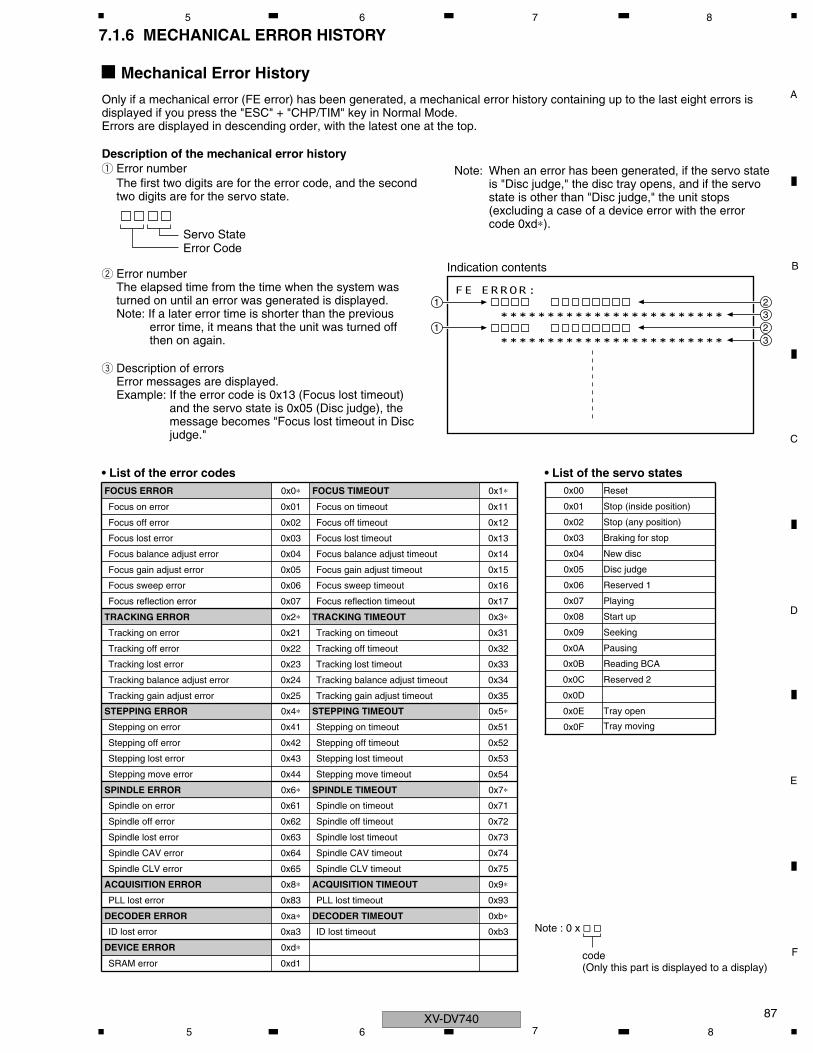
C
D
F
A
B
E
87
5 6 7 8
7.1.6 MECHANICAL ERROR HISTORY
Indication contents
• List of the error codes • List of the servo states
Note : 0 x & &
code(Only this part is displayed to a display)
1 23
Description of the mechanical error history1 Error number
The first two digits are for the error code, and the second two digits are for the servo state.
2 Error numberThe elapsed time from the time when the system was turned on until an error was generated is displayed.Note: If a later error time is shorter than the previous
error time, it means that the unit was turned off then on again.
3 Description of errorsError messages are displayed.Example: If the error code is 0x13 (Focus lost timeout)
and the servo state is 0x05 (Disc judge), the message becomes "Focus lost timeout in Disc judge."
Only if a mechanical error (FE error) has been generated, a mechanical error history containing up to the last eight errors is displayed if you press the "ESC" + "CHP/TIM" key in Normal Mode.Errors are displayed in descending order, with the latest one at the top.
Error CodeServo State
1 23
0x00 Reset
0x01 Stop (inside position)
0x02 Stop (any position)
0x03 Braking for stop
0x04 New disc
0x05 Disc judge
0x06 Reserved 1
0x07 Playing
0x08 Start up
0x09 Seeking
0x0A Pausing
0x0B Reading BCA
0x0C Reserved 2
Tray open
Tray moving
0x0D
0x0E
0x0F
FOCUS ERROR 0x0∗ FOCUS TIMEOUT 0x1∗
Focus on error 0x01 Focus on timeout 0x11
Focus off error 0x02 Focus off timeout 0x12
Focus lost error 0x03 Focus lost timeout 0x13
Focus balance adjust error 0x04 Focus balance adjust timeout 0x14
Focus gain adjust error 0x05 Focus gain adjust timeout 0x15
Focus sweep error 0x06 Focus sweep timeout 0x16
Focus reflection error 0x07 Focus reflection timeout 0x17
TRACKING ERROR 0x2∗ TRACKING TIMEOUT 0x3∗
Tracking on error 0x21 Tracking on timeout 0x31
Tracking off error 0x22 Tracking off timeout 0x32
Tracking lost error 0x23 Tracking lost timeout 0x33
Tracking balance adjust error 0x24 Tracking balance adjust timeout 0x34
Tracking gain adjust error 0x25 Tracking gain adjust timeout 0x35
STEPPING ERROR 0x4∗ STEPPING TIMEOUT 0x5∗
Stepping on error 0x41 Stepping on timeout 0x51
Stepping off error 0x42 Stepping off timeout 0x52
Stepping lost error 0x43 Stepping lost timeout 0x53
Stepping move error 0x44 Stepping move timeout 0x54
SPINDLE ERROR 0x6∗ SPINDLE TIMEOUT 0x7∗
Spindle on error 0x61 Spindle on timeout 0x71
Spindle off error 0x62 Spindle off timeout 0x72
Spindle lost error 0x63 Spindle lost timeout 0x73
Spindle CAV error 0x64 Spindle CAV timeout 0x74
Spindle CLV error 0x65 Spindle CLV timeout 0x75
ACQUISITION ERROR 0x8∗ ACQUISITION TIMEOUT 0x9∗
PLL lost error 0x83 PLL lost timeout 0x93
DECODER ERROR 0xa∗ DECODER TIMEOUT 0xb∗
ID lost error 0xa3 ID lost timeout 0xb3
DEVICE ERROR 0xd∗
SRAM error 0xd1
Note: When an error has been generated, if the servo state is "Disc judge," the disc tray opens, and if the servo state is other than "Disc judge," the unit stops (excluding a case of a device error with the error code 0xd∗).
Mechanical Error History
XV-DV7405 6 7 8
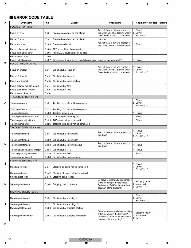
C
D
F
A
B
E
XV-DV74088
1 2 3 4
Error Name No. Causes Check Item Possibility of Trouble Remarks
FOCUS ERROR (0 x 0∗)
Focus on error 0 x 01 Focus on could not be completedAre not there a dirt or a scratch in the Disc? Does LD become weak?Does the lens move up and down?
1. Pickup2. Driver3. Front End IC
Focus off error 0 x 02 Focus off could not be completed Unknown
Focus lost error 0 x 03 Focus servo is lostAre not there a dirt or a scratch in the Disc? Does LD become weak?
1. Pickup
Focus balance adjust error 0 x 04 AFB on could not be completed
Focus gain adjust error 0 x 05 Focus AGC could not be completed
Focus sweep error 0 x 06
Focus reflection error 0 x 07 Dimensions of S curve did not reach to the aim value Does LD become weak? 1. Pickup
FOCUS TIMEOUT (0 x 1∗)
Focus on timeout 0 x 11 Did timeout at focus onAre not there a dirt or a scratch in the Disc? Does LD become weak?Does the lens move up and down?
1. Pickup2. Driver3. Front End IC
Focus off timeout 0 x 12 Did timeout at focus off
Focus lost timeout 0 x 13 Did timeout at focus backup
Focus balance adjust timeout 0 x 14 Did timeout at AFB
Focus gain adjust timeout 0 x 15 Did timeout at AGC
Focus sweep timeout 0 x 16
TRACKING ERROR (0 x 2∗)
Tracking on error 0 x 21 Tracking on could not be completed1. Pickup2. Driver3. Front End IC
Tracking off error 0 x 22 Tracking off could not be completed
Tracking lost error 0 x 23 Tracking servo is lost 1. Pickup
Tracking balance adjust error 0 x 24 ATB could not be completed 1. Pickup
Tracking gain adjust error 0 x 25 AGC could not be completed 1. Pickup
Tracking jump error 0 x 26 Tracking jump could not be completed
TRACKING TIMEOUT (0 x 3∗)
Tracking on timeout 0 x 31 Did timeout at tracking onAre not there a dirt or a scratch in the Disc?
1. Pickup2. Driver3. Front End IC
Tracking off timeout 0 x 32 Did timeout at tracking off
Tracking lost timeout 0 x 33 Did timeout at tracking backupAre not there a dirt or a scratch in the Disc? 1. Pickup
Tracking balance adjust timeout 0 x 34 Did timeout at ATB 1. Pickup
Tracking gain adjust timeout 0 x 35 Did timeout at AGC 1. Pickup
Tracking jump timeout 0 x 36 Did timeout at tracking jump
STEPPING ERROR (0 x 4∗)
Stepping on error 0 x 41 Stepping on could not be completed1. Pickup2. Driver3. Front End IC
Stepping off error 0 x 42 Stepping off could not be completed
Stepping lost error 0 x 43 Stepping servo is lost
Stepping move error 0 x 44 Stepping could not move
Do move to inner and outer periphery of the stepping in the test mode?Do indicate "S-04" at the most inner periphery of the stepping?
1. Stepping motor2. Inside switch3. Driver
STEPPING TIMEOUT (0 x 5∗)
Stepping on timeout 0 x 51 Did timeout at stepping on1. Pickup2. Driver3. Front End IC
Stepping off timeout 0 x 52 Did timeout at stepping off
Stepping lost timeout 0 x 53 Did timeout at stepping backup
Stepping move timeout 0 x 54 Did timeout at stepping movement
Do move to inner and outer periphery of the stepping in the test mode?Do indicate "S-04" at the most inner periphery of the stepping?
1. Stepping motor2. Inside switch3. Driver
ERROR CODE TABLE
1 2 3 4
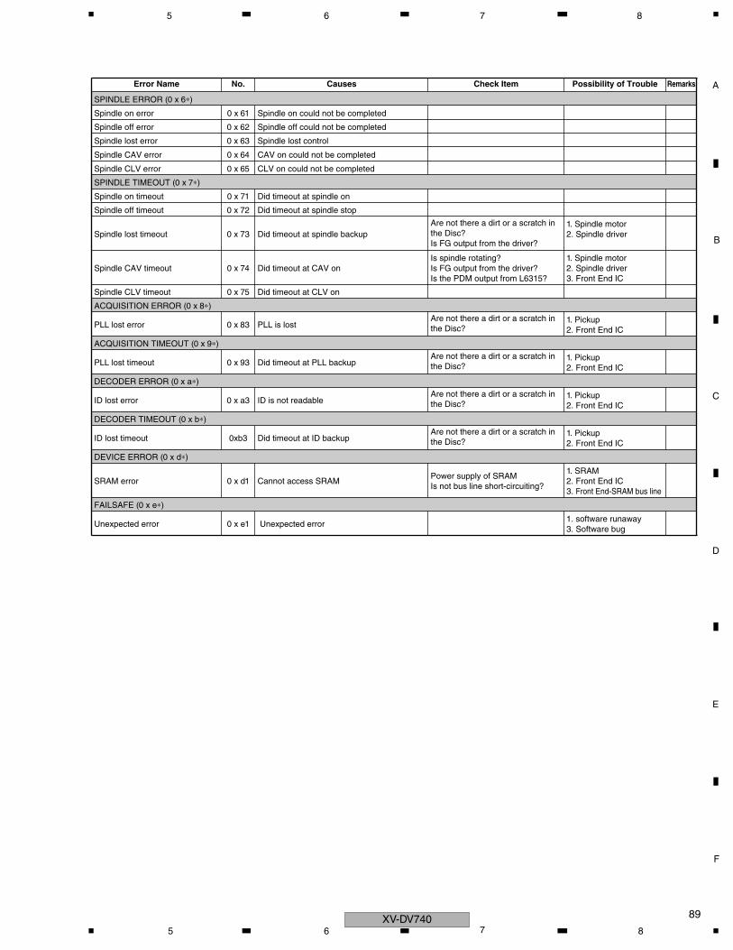
C
D
F
A
B
E
89
5 6 7 8
Error Name No. Causes Check Item Possibility of Trouble Remarks
SPINDLE ERROR (0 x 6∗)
Spindle on error 0 x 61 Spindle on could not be completed
Spindle off error 0 x 62 Spindle off could not be completed
Spindle lost error 0 x 63 Spindle lost control
Spindle CAV error 0 x 64 CAV on could not be completed
Spindle CLV error 0 x 65 CLV on could not be completed
SPINDLE TIMEOUT (0 x 7∗)
Spindle on timeout 0 x 71 Did timeout at spindle on
Spindle off timeout 0 x 72 Did timeout at spindle stop
Spindle lost timeout 0 x 73 Did timeout at spindle backupAre not there a dirt or a scratch in the Disc?Is FG output from the driver?
1. Spindle motor2. Spindle driver
Spindle CAV timeout 0 x 74 Did timeout at CAV onIs spindle rotating?Is FG output from the driver?Is the PDM output from L6315?
1. Spindle motor2. Spindle driver3. Front End IC
Spindle CLV timeout 0 x 75 Did timeout at CLV on
ACQUISITION ERROR (0 x 8∗)
PLL lost error 0 x 83 PLL is lostAre not there a dirt or a scratch in the Disc?
1. Pickup2. Front End IC
ACQUISITION TIMEOUT (0 x 9∗)
PLL lost timeout 0 x 93 Did timeout at PLL backupAre not there a dirt or a scratch in the Disc?
1. Pickup2. Front End IC
DECODER ERROR (0 x a∗)
ID lost error 0 x a3 ID is not readableAre not there a dirt or a scratch in the Disc?
1. Pickup2. Front End IC
DECODER TIMEOUT (0 x b∗)
ID lost timeout 0xb3 Did timeout at ID backupAre not there a dirt or a scratch in the Disc?
1. Pickup2. Front End IC
DEVICE ERROR (0 x d∗)
SRAM error 0 x d1 Cannot access SRAMPower supply of SRAMIs not bus line short-circuiting?
1. SRAM2. Front End IC3. Front End-SRAM bus line
FAILSAFE (0 x e∗)
Unexpected error 0 x e1 Unexpected error1. software runaway3. Software bug
XV-DV7405 6 7 8
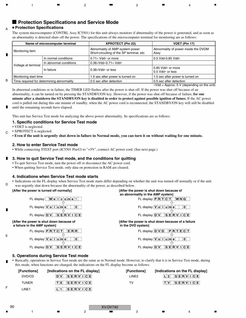
C
D
F
A
B
E
XV-DV74090
1 2 3 4
Protection Specifications and Service Mode
1. Specific conditions for Service Test mode• VDET is neglected.• XPROTECT is neglected.• Even if the unit is urgently shut down in failure in Normal mode, you can turn it on without waiting for one minute.
2. How to enter Service Test mode• While connecting STEST port (IC5501 Pin43) to "+5V", connect AC power cord. (See next page.)
3. How to quit Service Test mode, and the conditions for quitting• To quit Service Test mode, turn the power off or disconnect the AC power cord.• When quitting Service Test mode, only data on protection in RAM are cleared.
4. Indications when Service Test mode starts• Indications on the FL display when Service Test mode starts differ depending on whether the unit was turned off normally or if the unit
was urgently shut down because the abnormality of the power, as described below.
Protection SpecificationsThe system microcomputer (CONTRL Assy IC5501) for this unit always monitors if abnormality of the power is generated, and as soon as an abnormality is detected shuts off the power. The specifications of the microcomputer terminal for monitoring are as follows:
In abnormal conditions or in failure, the TIMER LED flashes after the power is shut off. If the power was shut off because of an abnormality, it can be turned on by pressing the STANDBY/ON key. However, if the power was shut off because of failure, for one minute after a shutdown the STANDBY/ON key is disabled in order to protect against possible ignition of fumes. If the AC power cord is pulled out during this one minute of standby, when the AC power cord is reconnected, the STANDBY/ON key will still be disabled until the remaining seconds have elapsed.
This unit has Service Test mode for analyzing the above power abnormality. Its specifications are as follows:
∗Vdd = Approx. 5 V (depending on the unit)
5. Operations during Service Test mode• Basically, operations in Service Test mode are the same as in Normal mode. However, to clarify that it is in Service Test mode, during
this mode, when functions are changed, the indications on the FL display become as follows:
W e l c o m e !
[After the power is turned off normally] [After the power is shut down because of an abnormality in the AMP system]
FL display
V o l u m e 0FL display
D V S E R V I C EFL display
P R T C T W N GFL display
V o l u m e 0FL display
D V S E R V I C EFL display
P R T C T E R RFL display
V o l u m e 0FL display
D V S E R V I C EFL display
D V S E R V I C EDVD/CD
T X S E R V I C ETUNER
L 1 S E R V I C ELINE1
D V D P R T E C TFL display
V o l u m e 0FL display
D V S E R V I C EFL display
[After the power is shut down because of a failure in the AMP system]
[After the power is shut down because of a failure in the DVD system]
Name of microcomputer terminal XPROTECT (Pin 22) VDET (Pin 17)
Monitoring itemAbnormality of AMP-system powerShort-circuiting of the SP terminal, etc.
Abnormality of power inside the DVDM Assy
Voltage at terminal
In normal conditions 0.71× Vdd∗ or more 0.5 Vdd-0.85 Vdd∗In abnormal conditions 0.36×Vdd–0.71× Vdd∗
In failure 0.36×Vdd∗ or less0.85 Vdd∗ or more0.5 Vdd∗ or less
Monitoring start time 1.5 sec after power is turned on 1.5 sec after power is turned onTime required for determining abnormality 0.5 sec after detection 0.5 sec after detection
[Functions] [Indications on the FL display]L 2 S E R V I C ELINE2
T V S E R V I C ETV
[Functions] [Indications on the FL display]
1 2 3 4
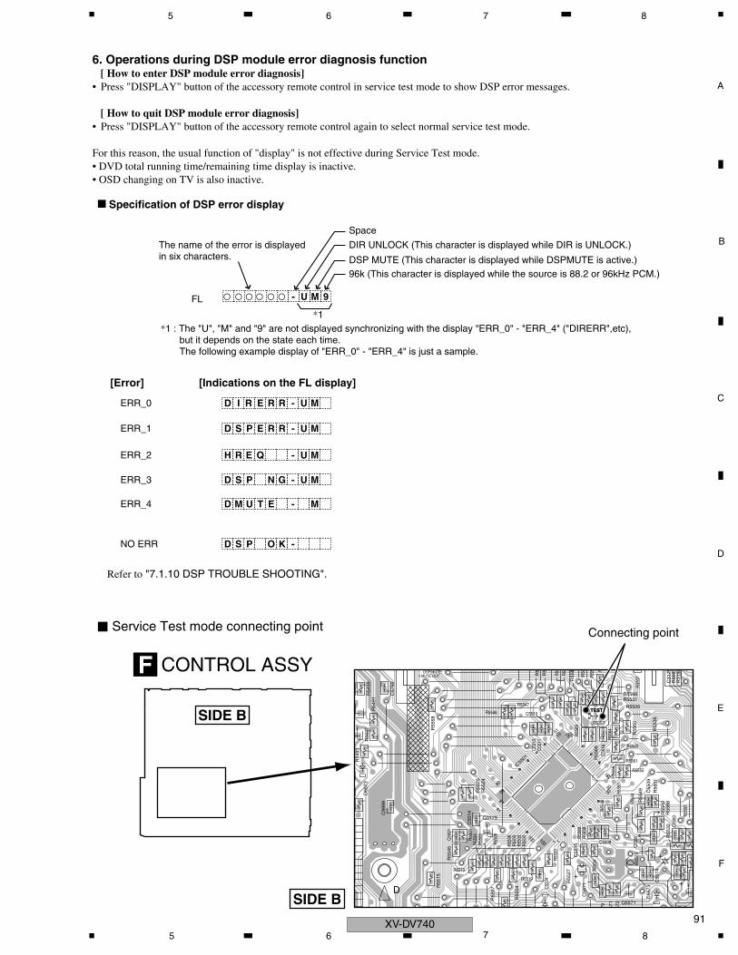
C
D
F
A
B
E
91
5 6 7 8
100
81
1
30
31
5051
80R55
25
C55
01
R55
15
R54
93
D55
73
R550
8
R55
27
C55
13
R550
6
R55
48
R555
0
R55
20
R55
39
79
R55
01
R55
24
R550
5
R55
R55
04
R55
8
R56
01
R550
9
R31
95R
5591
C55
80
C55
09
R55
69
R5
C5510
C31
75
R55
07
R55
60
R5561
R5547
R5546
R55
R55
89
C55
14R5
554
R54
91
R5563
C57
92
C55
15
C550
4
R556
4
R55
68
R5
C55
11
R55
35
R37
07
R553
4
C550
6
R30
91
R55
C55
16R
R55
45
Q5571
C5508
R54
99
C99
99
R55
49
R56
22
R55
40
R550
2R5
503
R5526
C55
71
6
R55
73
4
C55
73
R5510
R55
32
C55
74
IC55
01
572
571
R554
4
R5555
R55
56
R55
R5519
Q3173
R5531
R55
88
R5566
R55
58
TEST
UTEST
D
1.MUTE OUTDSP MUTE
1
30
31
5051
80
81
100
6. Operations during DSP module error diagnosis function [ How to enter DSP module error diagnosis]• Press "DISPLAY" button of the accessory remote control in service test mode to show DSP error messages.
[ How to quit DSP module error diagnosis]• Press "DISPLAY" button of the accessory remote control again to select normal service test mode.
For this reason, the usual function of "display" is not effective during Service Test mode.• DVD total running time/remaining time display is inactive.• OSD changing on TV is also inactive.
D I R E R R - U M
- U M 9
ERR_0
FL
Space
DIR UNLOCK (This character is displayed while DIR is UNLOCK.)
DSP MUTE (This character is displayed while DSPMUTE is active.)96k (This character is displayed while the source is 88.2 or 96kHz PCM.)
*1 : The "U", "M" and "9" are not displayed synchronizing with the display "ERR_0" - "ERR_4" ("DIRERR",etc), but it depends on the state each time. The following example display of "ERR_0" - "ERR_4" is just a sample.
The name of the error is displayedin six characters.
‡ ‡ ‡ ‡ ‡ ‡
D S P E R R - U MERR_1
H R E Q - U MERR_2
D S P N -G U MERR_3
D M TU E - MERR_4
Refer to "7.1.10 DSP TROUBLE SHOOTING".
D S P O K -NO ERR
[Error] [Indications on the FL display]
Specification of DSP error display
*1
TEST
SIDE B
SIDE B
CONTROL ASSY
Connecting pointService Test mode connecting point
F
XV-DV7405 6 7 8
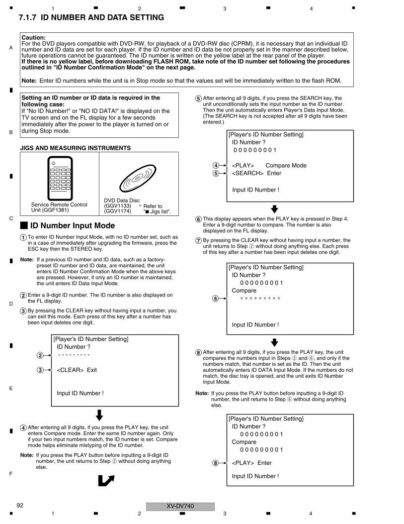
C
D
F
A
B
E
XV-DV74092
1 2 3 4
7.1.7 ID NUMBER AND DATA SETTING
To enter ID Number Input Mode, with no ID number set, such as in a case of immediately after upgrading the firmware, press the ESC key then the STEREO key.
Note: If a previous ID number and ID data, such as a factory-preset ID number and ID data, are maintained, the unit enters ID Number Confirmation Mode when the above keys are pressed. However, if only an ID number is maintained, the unit enters ID Data Input Mode.
ID Number Input Mode
[Player's ID Number Setting] ID Number ? - - - - - - - - -
<CLEAR> Exit
Input ID Number !
1
This display appears when the PLAY key is pressed in Step 4. Enter a 9-digit number to compare. The number is also displayed on the FL display.
6
By pressing the CLEAR key without having input a number, the unit returns to Step 2 without doing anything else. Each press of this key after a number has been input deletes one digit.
7
After entering all 9 digits, if you press the PLAY key, the unit compares the numbers input in Steps 2 and 6, and only if the numbers match, that number is set as the ID. Then the unit automatically enters ID DATA Input Mode. If the numbers do not match, the disc tray is opened, and the unit exits ID Number Input Mode.
8
Enter a 9-digit ID number. The ID number is also displayed on the FL display.
2
By pressing the CLEAR key without having input a number, you can exit this mode. Each press of this key after a number has been input deletes one digit.
3
After entering all 9 digits, if you press the PLAY key, the unit enters Compare mode. Enter the same ID number again. Only if your two input numbers match, the ID number is set. Compare mode helps eliminate mistyping of the ID number.
4
2
3
[Player's ID Number Setting] ID Number ? 0 0 0 0 0 0 0 0 1 Compare ∗ ∗ ∗ ∗ ∗ ∗ ∗ ∗ ∗
Input ID Number !
6
[Player's ID Number Setting] ID Number ? 0 0 0 0 0 0 0 0 1 Compare 0 0 0 0 0 0 0 0 1
<PLAY> Enter
Input ID Number !
8
Input ID Number !
After entering all 9 digits, if you press the SEARCH key, the unit unconditionally sets the input number as the ID number. Then the unit automatically enters Player's Data Input Mode. (The SEARCH key is not accepted after all 9 digits have been entered.)
5
[Player's ID Number Setting] ID Number ? 0 0 0 0 0 0 0 0 1
<PLAY> Compare Mode <SEARCH> Enter
4
5
Caution:For the DVD players compatible with DVD-RW, for playback of a DVD-RW disc (CPRM), it is necessary that an individual ID number and ID data are set for each player. If the ID number and ID data be not properly set in the manner described below, future operations cannot be guaranteed. The ID number is written on the yellow label at the rear panel of the player.If there is no yellow label, before downloading FLASH ROM, take note of the ID number set following the procedures outlined in "ID Number Confirmation Mode" on the next page.
Note: Enter ID numbers while the unit is in Stop mode so that the values set will be immediately written to the flash ROM.
Note: If you press the PLAY button before inputting a 9-digit ID number, the unit returns to Step 2 without doing anything else.
Note: If you press the PLAY button before inputting a 9-digit ID number, the unit returns to Step 6 without doing anything else.
DVD Data Disc(GGV1133)(GGV1174)
Service Remote ControlUnit (GGF1381)
JIGS AND MEASURING INSTRUMENTS
Setting an ID number or ID data is required in the following case:If "No ID Number!" or "NO ID DATA!" is displayed on the TV screen and on the FL display for a few seconds immediately after the power to the player is turned on or during Stop mode.
* Refer to "7 Jigs list".
1 2 3 4
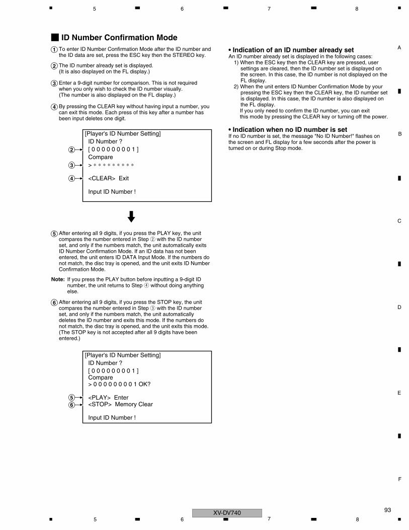
C
D
F
A
B
E
93
5 6 7 8
To enter ID Number Confirmation Mode after the ID number and the ID data are set, press the ESC key then the STEREO key.
ID Number Confirmation Mode1
The ID number already set is displayed.(It is also displayed on the FL display.)
2
Enter a 9-digit number for comparison. This is not required when you only wish to check the ID number visually.(The number is also displayed on the FL display.)
3
By pressing the CLEAR key without having input a number, you can exit this mode. Each press of this key after a number has been input deletes one digit.
4
After entering all 9 digits, if you press the PLAY key, the unit compares the number entered in Step 2 with the ID number set, and only if the numbers match, the unit automatically exits ID Number Confirmation Mode. If an ID data has not been entered, the unit enters ID DATA Input Mode. If the numbers do not match, the disc tray is opened, and the unit exits ID Number Confirmation Mode.
5
After entering all 9 digits, if you press the STOP key, the unit compares the number entered in Step 3 with the ID number set, and only if the numbers match, the unit automatically deletes the ID number and exits this mode. If the numbers do not match, the disc tray is opened, and the unit exits this mode.(The STOP key is not accepted after all 9 digits have been entered.)
6
[Player's ID Number Setting] ID Number ? [ 0 0 0 0 0 0 0 0 1 ] Compare > ∗ ∗ ∗ ∗ ∗ ∗ ∗ ∗ ∗
<CLEAR> Exit
Input ID Number !
3
2
4
[Player's ID Number Setting] ID Number ? [ 0 0 0 0 0 0 0 0 1 ] Compare > 0 0 0 0 0 0 0 0 1 OK?
<PLAY> Enter <STOP> Memory Clear
Input ID Number !
56
Note: If you press the PLAY button before inputting a 9-digit ID number, the unit returns to Step 4 without doing anything else.
• Indication of an ID number already setAn ID number already set is displayed in the following cases:
1) When the ESC key then the CLEAR key are pressed, user settings are cleared, then the ID number set is displayed on the screen. In this case, the ID number is not displayed on the FL display.
2) When the unit enters ID Number Confirmation Mode by your pressing the ESC key then the CLEAR key, the ID number set is displayed. In this case, the ID number is also displayed on the FL display.If you only need to confirm the ID number, you can exit this mode by pressing the CLEAR key or turning off the power.
• Indication when no ID number is setIf no ID number is set, the message "No ID Number!" flashes on the screen and FL display for a few seconds after the power is turned on or during Stop mode.
XV-DV7405 6 7 8
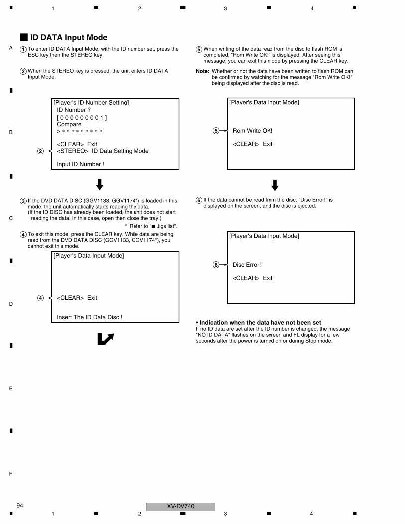
C
D
F
A
B
E
XV-DV74094
1 2 3 4
To enter ID DATA Input Mode, with the ID number set, press the ESC key then the STEREO key.
ID DATA Input Mode1 When writing of the data read from the disc to flash ROM is
completed, "Rom Write OK!" is displayed. After seeing this message, you can exit this mode by pressing the CLEAR key.
5
If the data cannot be read from the disc, "Disc Error!" is displayed on the screen, and the disc is ejected.
6
When the STEREO key is pressed, the unit enters ID DATA Input Mode.
2
If the DVD DATA DISC (GGV1133, GGV1174*) is loaded in this mode, the unit automatically starts reading the data.(If the ID DISC has already been loaded, the unit does not start reading the data. In this case, open then close the tray.)
3
To exit this mode, press the CLEAR key. While data are being read from the DVD DATA DISC (GGV1133, GGV1174*), you cannot exit this mode.
4
[Player's ID Number Setting] ID Number ? [ 0 0 0 0 0 0 0 0 1 ] Compare > ∗ ∗ ∗ ∗ ∗ ∗ ∗ ∗ ∗
<CLEAR> Exit <STEREO> ID Data Setting Mode
Input ID Number !
2
[Player's Data Input Mode]
<CLEAR> Exit
Insert The ID Data Disc !
4
[Player's Data Input Mode]
Rom Write OK!
<CLEAR> Exit
5
[Player's Data Input Mode]
Disc Error!
<CLEAR> Exit
6
Note: Whether or not the data have been written to flash ROM can be confirmed by watching for the message "Rom Write OK!" being displayed after the disc is read.
• Indication when the data have not been setIf no ID data are set after the ID number is changed, the message "NO ID DATA" flashes on the screen and FL display for a few seconds after the power is turned on or during Stop mode.
* Refer to "7 Jigs list".
1 2 3 4
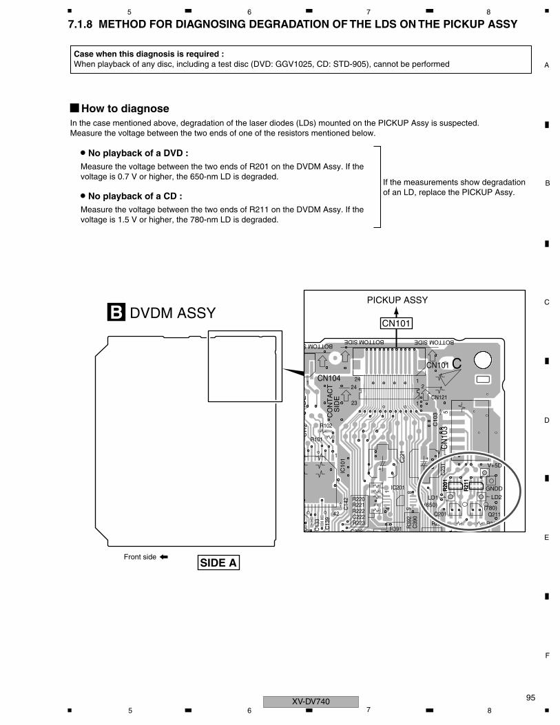
C
D
F
A
B
E
95
5 6 7 8
7.1.8 METHOD FOR DIAGNOSING DEGRADATION OF THE LDS ON THE PICKUP ASSY
1
58
51
14
124
42
1
24
23
2
1
C23
1
R102
CN104
CN
103
R202
IC201
C22
1
R20
1
R221
R223
R222
R101
C222
C13
9
C14
2
CN101
R212
R21
1
IC10
1
C11
2
Q201
R220
R39
2
R391 C39
0 Q211
C306C13
3
CN121
C10
3CO
NT
AC
TS
IDE
BOTTOM SIDEBOTTOM S
BOTTOM SIDE
C
(650)
IDE
(780)
GNDD
V+5D
LD2LD1
Case when this diagnosis is required : When playback of any disc, including a test disc (DVD: GGV1025, CD: STD-905), cannot be performed
How to diagnoseIn the case mentioned above, degradation of the laser diodes (LDs) mounted on the PICKUP Assy is suspected.Measure the voltage between the two ends of one of the resistors mentioned below.
Measure the voltage between the two ends of R201 on the DVDM Assy. If the voltage is 0.7 V or higher, the 650-nm LD is degraded.
No playback of a DVD :
Measure the voltage between the two ends of R211 on the DVDM Assy. If the voltage is 1.5 V or higher, the 780-nm LD is degraded.
No playback of a CD :
If the measurements show degradation of an LD, replace the PICKUP Assy.
PICKUP ASSY
CN101
SIDE A
DVDM ASSY
Front side
B
R20
1
R21
1
XV-DV7405 6 7 8
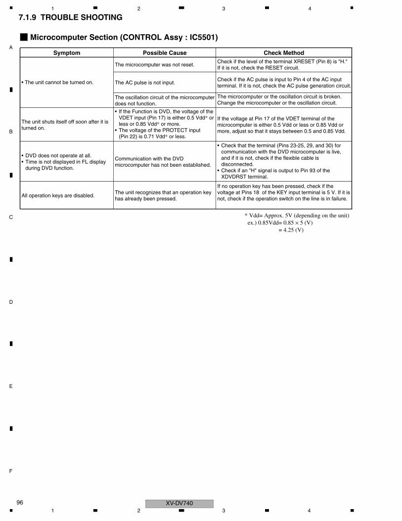
C
D
F
A
B
E
XV-DV74096
1 2 3 4
7.1.9 TROUBLE SHOOTING
Microcomputer Section (CONTROL Assy : IC5501)
Symptom Possible Cause Check Method
• The unit cannot be turned on.
The microcomputer was not reset.Check if the level of the terminal XRESET (Pin 8) is "H." If it is not, check the RESET circuit.
The AC pulse is not input.Check if the AC pulse is input to Pin 4 of the AC input terminal. If it is not, check the AC pulse generation circuit.
The oscillation circuit of the microcomputer does not function.
The microcomputer or the oscillation circuit is broken.Change the microcomputer or the oscillation circuit.
The unit shuts itself off soon after it is turned on.
• If the Function is DVD, the voltage of the VDET input (Pin 17) is either 0.5 Vdd* or less or 0.85 Vdd* or more.
• The voltage of the PROTECT input(Pin 22) is 0.71 Vdd* or less.
If the voltage at Pin 17 of the VDET terminal of the microcomputer is either 0.5 Vdd or less or 0.85 Vdd or more, adjust so that it stays between 0.5 and 0.85 Vdd.
• DVD does not operate at all.• Time is not displayed in FL display
during DVD function.
Communication with the DVD microcomputer has not been established.
• Check that the terminal (Pins 23-25, 29, and 30) for communication with the DVD microcomputer is live, and if it is not, check if the flexible cable is disconnected.
• Check if an "H" signal is output to Pin 93 of the XDVDRST terminal.
All operation keys are disabled.The unit recognizes that an operation key has already been pressed.
If no operation key has been pressed, check if the voltage at Pins 18 of the KEY input terminal is 5 V. If it is not, check if the operation switch on the line is in failure.
* Vdd= Approx. 5V (depending on the unit) ex.) 0.85Vdd= 0.85 × 5 (V) = 4.25 (V)
1 2 3 4
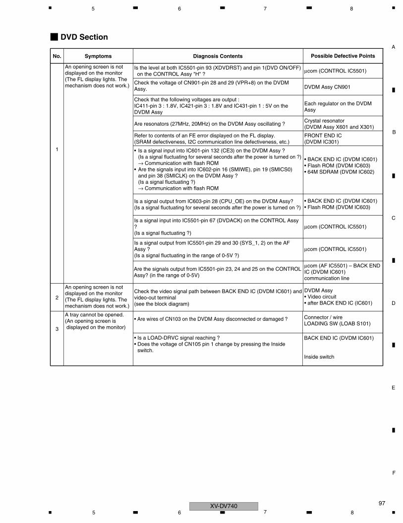
C
D
F
A
B
E
97
5 6 7 8
DVD Section
No. Symptoms Diagnosis Contents Possible Defective Points
1
An opening screen is not displayed on the monitor(The FL display lights. The mechanism does not work.)
Is the level at both IC5501-pin 93 (XDVDRST) and pin 1(DVD ON/OFF) on the CONTROL Assy "H" ?
µcom (CONTROL IC5501)
Check the voltage of CN901-pin 28 and 29 (VPR+8) on the DVDM Assy. DVDM Assy CN901
Check that the following voltages are output :IC411-pin 3 : 1.8V, IC421-pin 3 : 1.8V and IC431-pin 1 : 5V on theDVDM Assy
Each regulator on the DVDM Assy
Are resonators (27MHz, 20MHz) on the DVDM Assy oscillating ?Crystal resonator (DVDM Assy X601 and X301)
Refer to contents of an FE error displayed on the FL display.(SRAM defectiveness, I2C communication line defectiveness, etc.)
FRONT END IC(DVDM IC301)
• Is a signal input into IC601-pin 132 (CE3) on the DVDM Assy ?(Is a signal fluctuating for several seconds after the power is turned on ?) → Communication with flash ROM
• Are the signals input into IC602-pin 16 (SMIWE), pin 19 (SMICS0) and pin 38 (SMICLK) on the DVDM Assy ?(Is a signal fluctuating ?)→ Communication with flash ROM
• BACK END IC (DVDM IC601)• Flash ROM (DVDM IC603)• 64M SDRAM (DVDM IC602)
Is a signal output from IC603-pin 28 (CPU_OE) on the DVDM Assy? (Is a signal fluctuating for several seconds after the power is turned on ?)
µcom (CONTROL IC5501)Is a signal input into IC5501-pin 67 (DVDACK) on the CONTROL Assy ?(Is a signal fluctuating ?)
• BACK END IC (DVDM IC601)• Flash ROM (DVDM IC603)
Is a signal output from IC5501-pin 29 and 30 (SYS_1, 2) on the AF Assy ?(Is a signal fluctuating in the range of 0-5V ?)
µcom (CONTROL IC5501)
Are the signals output from IC5501-pin 23, 24 and 25 on the CONTROL Assy? (in the range of 0-5V)
µcom (AF IC5501) – BACK END IC (DVDM IC601) communication line
2
An opening screen is not displayed on the monitor(The FL display lights. The mechanism does not work.)
DVDM Assy• Video circuit• after BACK END IC (IC601)
3
A tray cannot be opened.(An opening screen is displayed on the monitor)
• Are wires of CN103 on the DVDM Assy disconnected or damaged ? Connector / wireLOADING SW (LOAB S101)
• Is a LOAD-DRVC signal reaching ?• Does the voltage of CN105 pin 1 change by pressing the Inside
switch.
BACK END IC (DVDM IC601)
Inside switch
Check the video signal path between BACK END IC (DVDM IC601) and video-out terminal(see the block diagram)
XV-DV7405 6 7 8
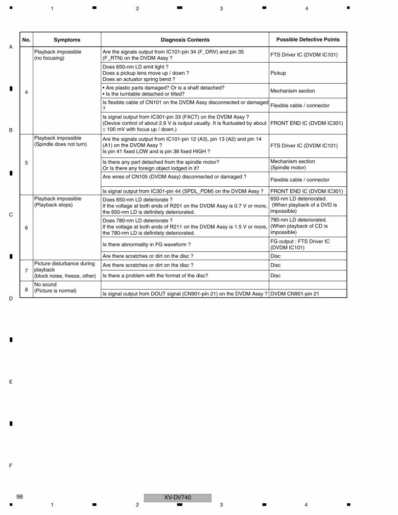
C
D
F
A
B
E
XV-DV74098
1 2 3 4
No. Symptoms Diagnosis Contents Possible Defective Points
4
Playback impossible(no focusing)
Are the signals output from IC101-pin 34 (F_DRV) and pin 35 (F_RTN) on the DVDM Assy ?
FTS Driver IC (DVDM IC101)
Does 650-nm LD emit light ?Does a pickup lens move up / down ?Does an actuator spring bend ?
Pickup
• Are plastic parts damaged? Or is a shaft detached?• Is the turntable detached or tilted?
Mechanism section
Is flexible cable of CN101 on the DVDM Assy disconnected or damaged ?
Flexible cable / connector
Is signal output from IC301-pin 33 (FACT) on the DVDM Assy ?(Device control of about 2.6 V is output usually. It is fluctuated by about ± 100 mV with focus up / down.)
FRONT END IC (DVDM IC301)
5
Playback impossible(Spindle does not turn)
Are the signals output from IC101-pin 12 (A3), pin 13 (A2) and pin 14 (A1) on the DVDM Assy ?Is pin 41 fixed LOW and is pin 38 fixed HIGH ?
FTS Driver IC (DVDM IC101)
Is there any part detached from the spindle motor? Or Is there any foreign object lodged in it?
Mechanism section(Spindle motor)
Are wires of CN105 (DVDM Assy) disconnected or damaged ?Flexible cable / connector
Is signal output from IC301-pin 44 (SPDL_PDM) on the DVDM Assy ? FRONT END IC (DVDM IC301)
6
Playback impossible(Playback stops)
Does 650-nm LD deteriorate ?If the voltage at both ends of R201 on the DVDM Assy is 0.7 V or more, the 650-nm LD is definitely deteriorated.
650-nm LD deteriorated. (When playback of a DVD is impossible)
Does 780-nm LD deteriorate ?If the voltage at both ends of R211 on the DVDM Assy is 1.5 V or more, the 780-nm LD is definitely deteriorated.
780-nm LD deteriorated.(When playback of CD is impossible)
Is there abnormality in FG waveform ?FG output : FTS Driver IC (DVDM IC101)
Are there scratches or dirt on the disc ? Disc
7Picture disturbance during playback(block noise, freeze, other)
8No sound(Picture is normal)
Is signal output from DOUT signal (CN901-pin 21) on the DVDM Assy ? DVDM CN901-pin 21
Are there scratches or dirt on the disc ? Disc
Is there a problem with the format of the disc? Disc
1 2 3 4

C
D
F
A
B
E
99
5 6 7 8
7.1.10 DSP TROUBLE SHOOTING
Detectable DSP Errors The following conditions are assumed, in order to eliminate causes other than "DSP-assy" and "between DSP-assy and microcomputers". • Electric power is correctly supplied to DSP-assy. • The SPDIF signal is coming to the input port of DIR ("COAX IN" RX0 & "OPT IN" RX3 & "DVD" RX7). • There is no audio output from DSP-assy, or audio output is unusual. Check the signal route by referring the connection diagram between U-com and DSP module IC (next page).
• ERR_0 : –Cannot receive data from DIR– →Communication fault has occurred somewhere between DIR (PinNo.32 CDTO)–Level Shifter (IC8702)– µ-com (PinNo.80 DIRDO). →Communication fault has occurred somewhere between the µ- com-port (*1) which has sent the signal and each IC.
• ERR_1 : –Cannot receive data from DSP– →Communication fault has occurred somewhere between DSP (PinNo.144 DSDO)–Level Shifter (IC8702)–µ-com (PinNo.50 DSPDO). →Communication fault has occurred somewhere between the µ-com-port (*1) which has sent the signal and each IC. →Communication fault has occurred somewhere between the DIR and DSP.
• ERR_2 : –There is no return value of HREQ.– →Communication fault has occurred somewhere between DSP (PinNo.3 HREQ)–Level Shifter (IC8702)–µ-com (PinNo.82 DSPHREQ). →Communication fault has occurred somewhere between the µ-com-port (*1) which has sent the signal and each IC. →Communication fault has occurred somewhere between the DIR and DSP.
• ERR_3 : –ERR information from DSP– →Communication fault has occurred somewhere between the µ-com-port (*1) which has sent the signal and each IC. (especially the fault inside DSP) →Communication fault has occurred somewhere between the DIR and DSP.
• ERR_4 : –DECOMUTE continues being LOW(MUTE).– →Communication fault has occurred somewhere between DSP (PinNo.21 PB12)–Level Shifter (IC8702)–µ-com (PinNo.86 DECMUTE). →Communication fault has occurred somewhere between the É com-port (*1) which has sent the signal and each IC. →Communication fault has occurred somewhere between the DIR and DSP.
Although the following are not errors, they are displayed separately and are helpful in finding a solution. • INFO_0 : –DIRERR is HIGH (UNLOCK) in digital function.– If DIRERR continues being HIGH (UNLOCK) without the above-mentioned error display. →Communication fault has occurred in somewhere between DIR (PinNo.36 INT0)–Level Shifter (IC8702)–µ-com (PinNo.77 DIRERR). →Check that the external set and this model is properly connected by the digital cable when selecting LINE2 (External Digital) function. • INFO_1 : –DSPMUTE is LOW (MUTE).– If DSPMUTE continues being LOW (MUTE) without the above-mentioned error display. →Communication fault has occurred somewhere between µ-com (PinNo.86 DSPMUTE)–connector (CN8011 and CN8012 No.19 MUTEOUT). • INFO_2 : –Loading 88.2kHz/96kHz PCM– DSP function is limited when this information is displayed. Notes : Only the high priority error (near to ERR_0) is displayed when the multiplel errors have occurred.
When the analog audio output of a DSP module is unusual but the above error information is not displayed, the fault is probably in the CODEC IC (IC8401) and the peripheral circuits. As the µ-com has not received data from the CODEC IC, it cannot detect the fault and display the error information.
D I R E R R - U MFL
FL
FL
FL
FL
D S P E R R - U M
H R E Q - U M
D S P N -G U M
D M TU E - M
FL D S P O K - MU
FL D S P O K - M
* "U", "M" display below is a sample. Those character display ON/OFF depends on the state.
FL D S P O K - 9
XV-DV7405 6 7 8
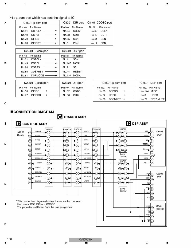
C
D
F
A
B
E
XV-DV740100
1 2 3 4
*1 : µ-com-port which has sent the signal to IC
IC5501 µ-com port IC8201 DIR port
Pin No. Pin NameNo.51 DSPCLK
No.49 DSPDI
No.79 DIRCS
No.78 DIRRST
Pin No. Pin NameNo.34 CCLK
No.33 CDTI
No.35 CSN
No.31 PDN
Pin No. Pin NameNo.42 CCLK
No.43 CDTI
No.41 CSN
No.17 PDN
IC8401 CODEC port
IC5501 µ-com port IC8501 DSP port
Pin No. Pin NameNo.51 DSPCLK
No.49 DSPDI
No.84 DSPSS
No.85 XDSPRST
Pin No. Pin NameNo.1 SCK
No.143 MOSI
No.2 SS
No.44 RESET
No.81 DSPMODE No.137 MODA
IC5501 µ-com port IC8201 DIR port
Pin No. Pin NameNo.80 DIRDO
No.77 DIRERR
Pin No. Pin NameNo.32 CDTO
No.36 INT0
IC5501 µ-com port IC8501 DSP port
Pin No. Pin NameNo.50 DSPDO
No.82 HREQ
No.86 DECMUTE
Pin No. Pin NameNo.144 MISO
No.3 HREQ
No.21 PB12 MUTE
IC5501CN5620 CN5619 CN5618 CN8011 IC8701
IC8501
DSP
Level Shifter
Level Shifter
IC8201DIR
IC8401CODEC
IC8702
DSPCLK SCK
DSPDI MOSI
DIRCS SS
DIRRST RESET
DSPSS MODA
XDSPRST MISO
DSPMODE HREQ
DIRDO PB12
DSPDO
DSPHREQCCLK
DECMUTECDTI
DIRERR
DSPCLK
DSPDI
DIRCS
DIRRST
DSPSS
XDSPRST
DSPMODE
DIRDO
DSPDO
DSPHREQ
DECMUTE
DIRERRCSN
PDN
CDTO
INT0
CCLK
CDTI
CSN
PDN
51
49
79
78
84
85
81
80
50
82
86
77
7
5
14
15
9
8
12
13
6
11
4
16
7
5
14
15
9
8
12
13
6
11
4
16
13
15
6
5
11
12
8
7
14
9
16
4
13
15
6
5
11
12
8
7
14
9
16
4
13
11
15
17
6
16
18
14
5
12
7
9
5
3
14
4
2
6
15
8
1
143
2
44
137
144
3
21
31
34
33
35
42
32
36
43
41
17
U-com
CONTROL ASSY
CONNECTION DIAGRAMTRADE 3 ASSY
DSP ASSY
* This connection diagram displays the connection between the U-com, DSP, DIR and CODEC. The pin order is different from the true assignment.
DG
C
1 2 3 4
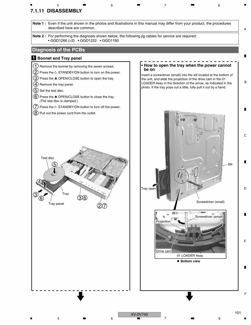
C
D
F
A
B
E
101
5 6 7 8
7.1.11 DISASSEMBLY
Bottom view
Diagnosis of the PCBs
Note 1 : Even if the unit shown in the photos and illustrations in this manual may differ from your product, the procedures described here are common.
Note 2 : For performing the diagnosis shown below, the following jig cables for service are required:• GGD1266 (×2) • GGD1222 • GGD1160
1 Remove the bonnet by removing the seven screws.
2 Press the STANDBY/ON button to turn on the power.
3 Press the 0 OPEN/CLOSE button to open the tray.
4 Remove the tray panel.
5 Set the test disc.
6 Press the 0 OPEN/CLOSE button to close the tray.(The test disc is clamped.)
7 Press the STANDBY/ON button to turn off the power.
8 Pull out the power cord from the outlet.
Bonnet and Tray panel1
36
4
2 7
3 6Tray panel
Tray
Test disc
5
How to open the tray when the power cannot be on
Slit
Tray open
Drive cam01 LOADER Assy
Screwdriver (small)
Screwdriver (small)
Projection
Insert a screwdriver (small) into the slit located at the bottom of the unit, and slide the projection of the drive cam in the 01 LOADER Assy in the direction of the arrow, as indicated in the photo. If the tray pops out a little, fully pull it out by a hand.
XV-DV7405 6 7 8
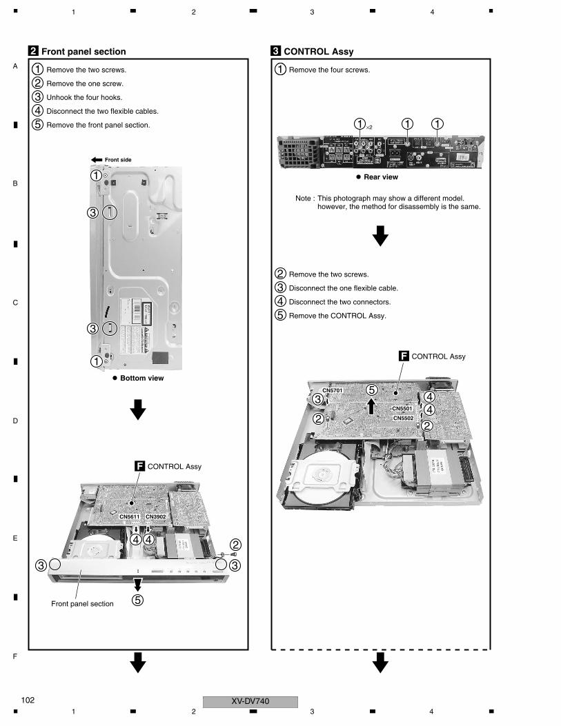
C
D
F
A
B
E
XV-DV740102
1 2 3 4
1 Remove the two screws.12 Remove the one screw.
3 Unhook the four hooks.
4 Disconnect the two flexible cables.
5 Remove the front panel section.
Front panel section2
2
5
33
4 4
3
3
1
Front panel section
CONTROL Assy
CN5611
CN5701
CN3902
45
4CN5501
CN5502
1
22
3
1Bottom view
Rear view
Front side
F
CONTROL AssyF
1 Remove the four screws.
×2
1
2 Remove the two screws.
3 Disconnect the one flexible cable.
4 Disconnect the two connectors.
5 Remove the CONTROL Assy.
CONTROL Assy3
1 1
Note : This photograph may show a different model. however, the method for disassembly is the same.
1 2 3 4
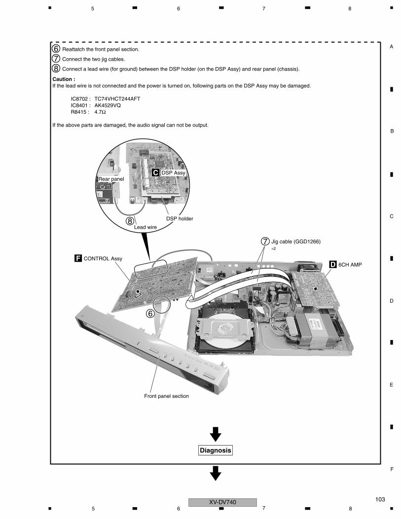
C
D
F
A
B
E
103
5 6 7 8
1 Connect the two jig cables.71 Reattatch the front panel section.6
1 Connect a lead wire (for ground) between the DSP holder (on the DSP Assy) and rear panel (chassis).
Caution :If the lead wire is not connected and the power is turned on, following parts on the DSP Assy may be damaged.
IC8702 : TC74VHCT244AFTIC8401 : AK4529VQR8415 : 4.7Ω
If the above parts are damaged, the audio signal can not be output.
8
DSP holder
Front panel section
Rear panel
Lead wire
DSP Assy
CONTROL Assy
Jig cable (GGD1266)×2
F6CH AMPD
C
8
7
6
Diagnosis
XV-DV7405 6 7 8
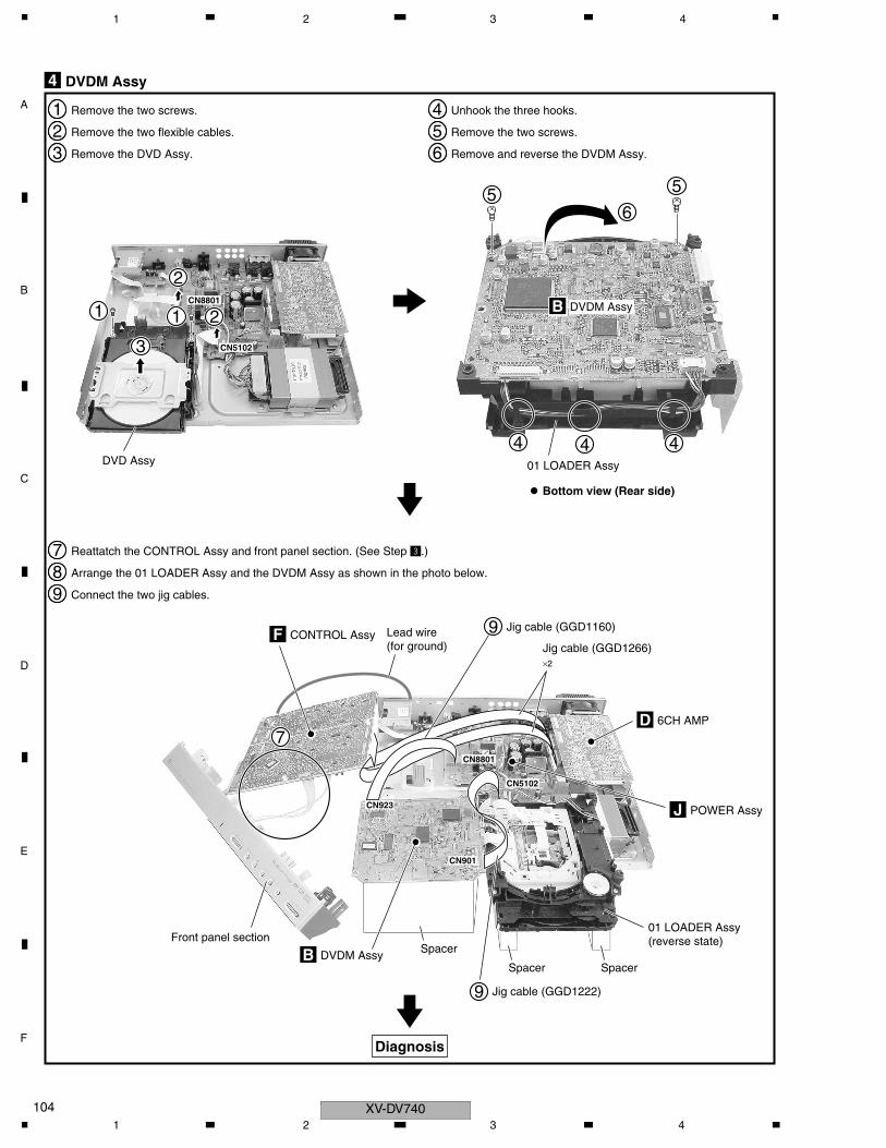
C
D
F
A
B
E
XV-DV740104
1 2 3 4
1 Remove the two screws.11 Remove the two flexible cables.21 Remove the DVD Assy.3
1 Reattatch the CONTROL Assy and front panel section. (See Step π.)71 Arrange the 01 LOADER Assy and the DVDM Assy as shown in the photo below.81 Connect the two jig cables.9
1 Unhook the three hooks.41 Remove the two screws.51 Remove and reverse the DVDM Assy.6
DVD Assy 01 LOADER Assy
Front panel section
CONTROL AssyF
6CH AMPD
POWER AssyJ
DVDM AssyB
DVDM AssyB
Diagnosis
DVDM Assy4
1 1
3
6
44
7
9
4
CN923
CN5102
CN8801
CN901
2
5
2CN8801
CN5102
5
Bottom view (Rear side)
Jig cable (GGD1266)×2
Jig cable (GGD1160)
9 Jig cable (GGD1222)
Lead wire(for ground)
01 LOADER Assy(reverse state)
SpacerSpacer
Spacer
1 2 3 4
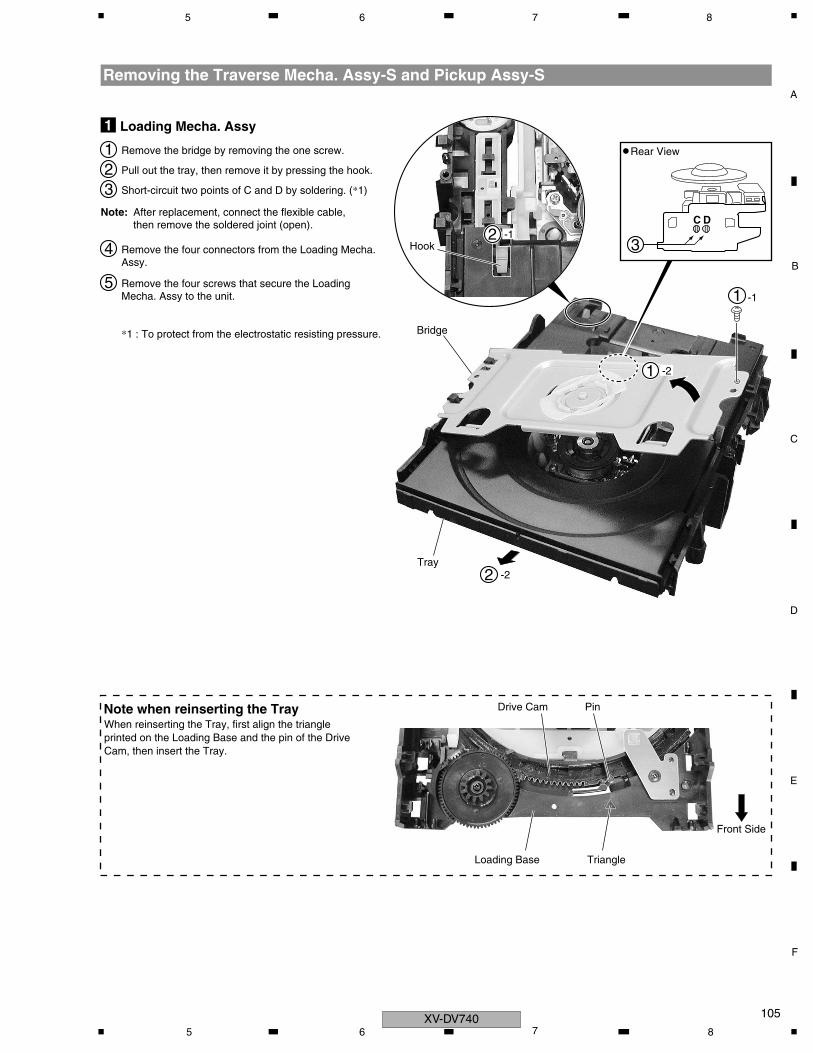
C
D
F
A
B
E
105
5 6 7 8
1 Remove the bridge by removing the one screw.
2 Pull out the tray, then remove it by pressing the hook.
3 Short-circuit two points of C and D by soldering. (*1)
4 Remove the four connectors from the Loading Mecha.Assy.
Note: After replacement, connect the flexible cable, then remove the soldered joint (open).
5 Remove the four screws that secure the LoadingMecha. Assy to the unit.
*1 : To protect from the electrostatic resisting pressure.
Loading Mecha. Assy1
Rear View
Front Side
1
3
-1
1 -2
2 -1
2 -2
Loading Base Triangle
Drive Cam Pin
Hook
Bridge
Tray
Note when reinserting the Tray
C D
Removing the Traverse Mecha. Assy-S and Pickup Assy-S
When reinserting the Tray, first align the triangle printed on the Loading Base and the pin of the Drive Cam, then insert the Tray.
XV-DV7405 6 7 8
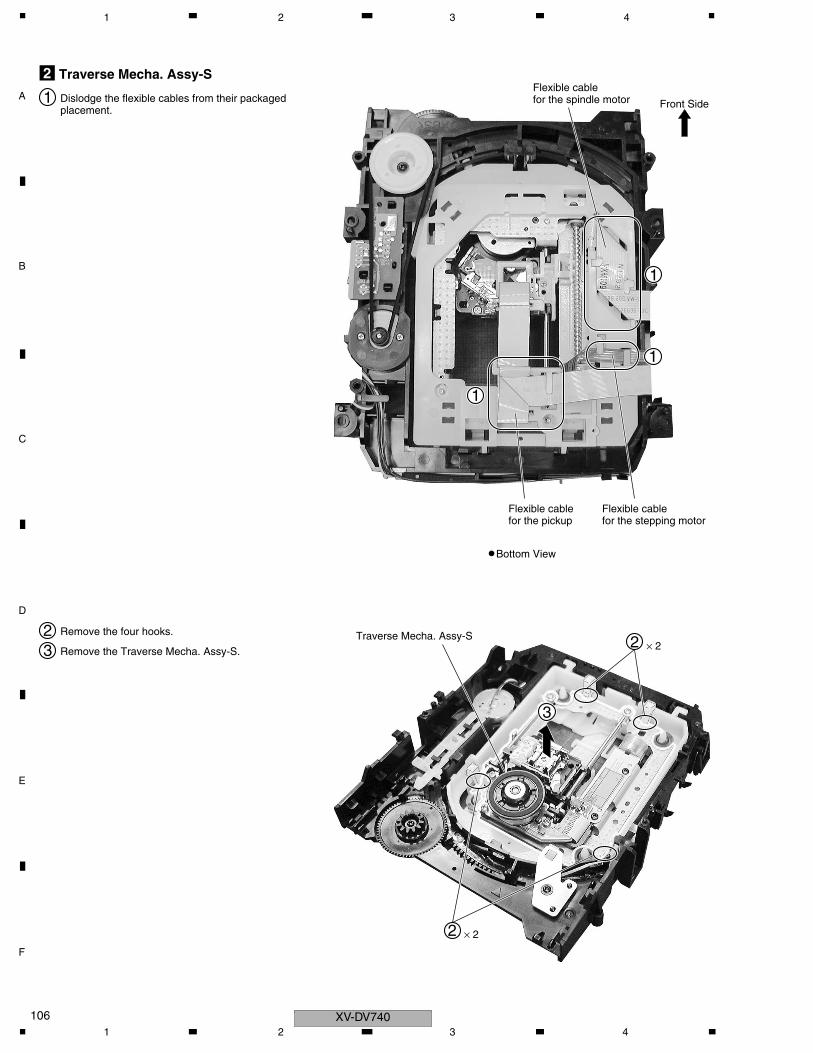
C
D
F
A
B
E
XV-DV740106
1 2 3 4
1 Dislodge the flexible cables from their packaged placement.
2 Remove the four hooks.
3 Remove the Traverse Mecha. Assy-S.
Traverse Mecha. Assy-S2
× 2
Bottom View
Traverse Mecha. Assy-S
Flexible cable for the pickup
Flexible cable for the spindle motor
1
1
1
2
× 22
3
Flexible cable for the stepping motor
Front Side
1 2 3 4
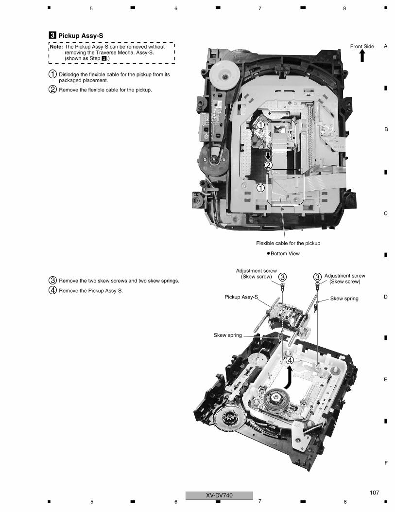
C
D
F
A
B
E
107
5 6 7 8
1 Dislodge the flexible cable for the pickup from its packaged placement.
2 Remove the flexible cable for the pickup.
3 Remove the two skew screws and two skew springs.
4 Remove the Pickup Assy-S.
Pickup Assy-S3
Note: The Pickup Assy-S can be removed without removing the Traverse Mecha. Assy-S. (shown as Step ø.)
Bottom View
Flexible cable for the pickup
1
4
33
1
2
Front Side
Pickup Assy-S
Adjustment screw(Skew screw) Adjustment screw
(Skew screw)
Skew spring
Skew spring
XV-DV7405 6 7 8
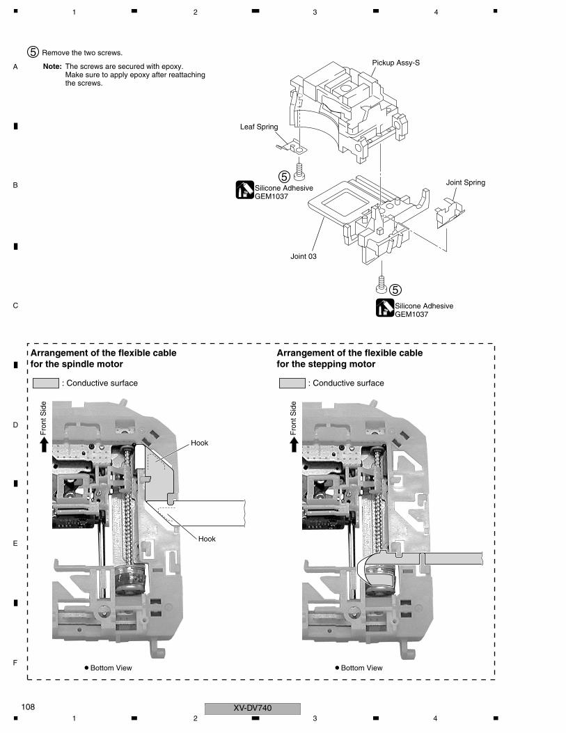
C
D
F
A
B
E
XV-DV740108
1 2 3 4
5
5
5
Remove the two screws.
Silicone AdhesiveGEM1037
Silicone AdhesiveGEM1037
Pickup Assy-SNote: The screws are secured with epoxy. Make sure to apply epoxy after reattaching the screws.
Leaf Spring
Joint Spring
Joint 03
: Conductive surface
Hook
Hook
Arrangement of the flexible cable for the spindle motor
: Conductive surface
Arrangement of the flexible cable for the stepping motor
Fro
nt S
ide
Fro
nt S
ide
Bottom View Bottom View
1 2 3 4
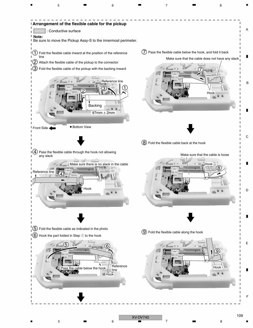
C
D
F
A
B
E
109
5 6 7 8
Front Side
Note: Be sure to move the Pickup Assy-S to the innermost perimeter.
: Conductive surface
Arrangement of the flexible cable for the pickup
2
213
7
Attach the flexible cable of the pickup to the connector
1 Fold the flexible cable inward at the position of the reference line
3 Fold the flexible cable of the pickup with the backing inward
7 Pass the flexible cable below the hook, and fold it back
8 Fold the flexible cable back at the hook
9 Fold the flexible cable along the hook
4 Pass the flexible cable through the hook not allowing any slack
6 Hook the part folded in Step 1 to the hook
5 Fold the flexible cable as indicated in the photo
Hook
Bottom View
5 6
Make sure there is no slack in the cable
Reference line
Reference line
Backing
97mm ± 2mm
Reference line
Hook
Pass the cable below the hook
Hook
8Hook
Hook
9
Make sure that the cable does not have any slack
Make sure that the cable is loose
4
XV-DV7405 6 7 8
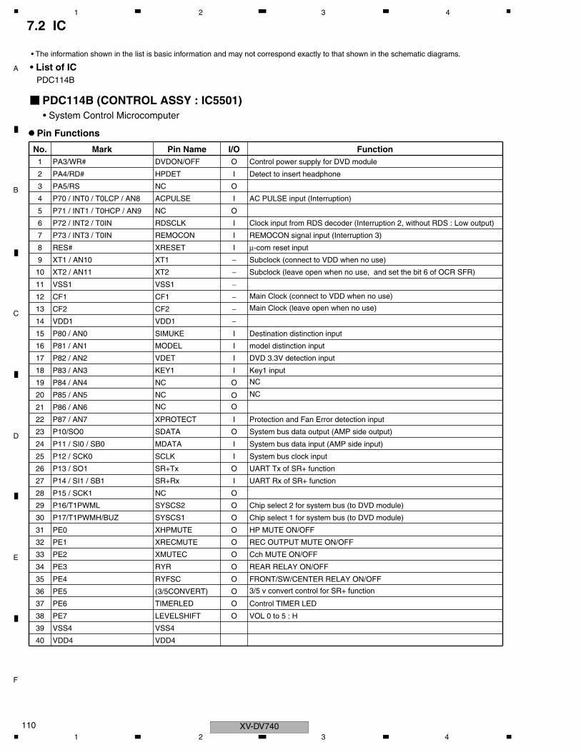
C
D
F
A
B
E
XV-DV740110
1 2 3 4
7.2 IC
PDC114B (CONTROL ASSY : IC5501)• System Control Microcomputer
Pin Functions
No. Mark Pin Name I/O Function1 PA3/WR# DVDON/OFF O Control power supply for DVD module
2 PA4/RD# HPDET I Detect to insert headphone
3 PA5/RS NC O
4 P70 / INT0 / T0LCP / AN8 ACPULSE I AC PULSE input (Interruption)
5 P71 / INT1 / T0HCP / AN9 NC O
6 P72 / INT2 / T0IN RDSCLK I Clock input from RDS decoder (Interruption 2, without RDS : Low output)
7 P73 / INT3 / T0IN REMOCON I REMOCON signal input (Interruption 3)
8 RES# XRESET I µ-com reset input
9 XT1 / AN10 XT1 − Subclock (connect to VDD when no use)
10 XT2 / AN11 XT2 − Subclock (leave open when no use, and set the bit 6 of OCR SFR)
11 VSS1 VSS1 −12 CF1 CF1 −13 CF2 CF2 −14 VDD1 VDD1 −15 P80 / AN0 SIMUKE I Destination distinction input
Main Clock (leave open when no use)
Main Clock (connect to VDD when no use)
16 P81 / AN1 MODEL I model distinction input
17 P82 / AN2 VDET I DVD 3.3V detection input
18 P83 / AN3 KEY1 I Key1 input
NC
NC
19 P84 / AN4 NC O
O20 P85 / AN5 NC
NC O21 P86 / AN6
22 P87 / AN7 XPROTECT I Protection and Fan Error detection input
23 P10/SO0 SDATA O System bus data output (AMP side output)
24 P11 / SI0 / SB0 MDATA I System bus data input (AMP side input)
25 P12 / SCK0 SCLK I System bus clock input
26 P13 / SO1 SR+Tx O UART Tx of SR+ function
27 P14 / SI1 / SB1 SR+Rx I UART Rx of SR+ function
28 P15 / SCK1 NC O
29 P16/T1PWML SYSCS2 O Chip select 2 for system bus (to DVD module)
30 P17/T1PWMH/BUZ SYSCS1 O Chip select 1 for system bus (to DVD module)
31 PE0 XHPMUTE O HP MUTE ON/OFF
32 PE1 XRECMUTE O REC OUTPUT MUTE ON/OFF
33 PE2 XMUTEC O Cch MUTE ON/OFF
34 PE3 RYR O REAR RELAY ON/OFF
35 PE4 RYFSC O FRONT/SW/CENTER RELAY ON/OFF
36 PE5 (3/5CONVERT) O
37 PE6 TIMERLED O Control TIMER LED
3/5 v convert control for SR+ function
38 PE7 LEVELSHIFT O VOL 0 to 5 : H
39 VSS4 VSS4
40 VDD4 VDD4
• The information shown in the list is basic information and may not correspond exactly to that shown in the schematic diagrams.
• List of ICPDC114B
1 2 3 4
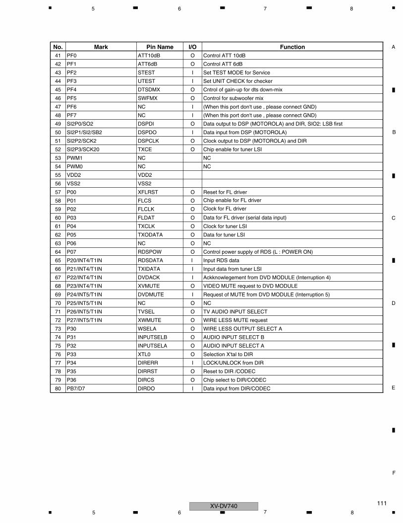
C
D
F
A
B
E
111
5 6 7 8
No. Mark Pin Name I/O Function41 PF0 ATT10dB O Control ATT 10dB
42 PF1 ATT6dB O Control ATT 6dB
43 PF2 STEST I Set TEST MODE for Service
44 PF3 UTEST I Set UNIT CHECK for checker
45 PF4 DTSDMX O Cntrol of gain-up for dts down-mix
46 PF5 SWFMX O Control for subwoofer mix
47 PF6 NC I (When this port don't use , please connect GND)
48 PF7 NC I (When this port don't use , please connect GND)
49 SI2P0/SO2 DSPDI O Data output to DSP (MOTOROLA) and DIR, SIO2: LSB first
50 SI2P1/SI2/SB2 DSPDO I Data input from DSP (MOTOROLA)
51 SI2P2/SCK2 DSPCLK O Clock output to DSP (MOTOROLA) and DIR
52 SI2P3/SCK20 TXCE O Chip enable for tuner LSI
53 PWM1 NC NC
54 PWM0 NC NC
55 VDD2 VDD2
56 VSS2 VSS2
57 P00 XFLRST O Reset for FL driver
Chip enable for FL driver
Clock for FL driver
Data for FL driver (serial data input)
58 P01 FLCS O
59 P02 FLCLK O
60 P03 FLDAT O
61 P04 TXCLK O Clock for tuner LSI
62 P05 TXODATA O Data for tuner LSI
63 P06 NC O NC
64 P07 RDSPOW O Control power supply of RDS (L : POWER ON)
65 P20/INT4/T1IN RDSDATA I Input RDS data
66 P21/INT4/T1IN TXIDATA I Input data from tuner LSI
67 P22/INT4/T1IN DVDACK I Ackknowlegement from DVD MODULE (Interruption 4)
68 P23/INT4/T1IN XVMUTE O VIDEO MUTE request to DVD MODULE
69 P24/INT5/T1IN DVDMUTE I Request of MUTE from DVD MODULE (Interruption 5)
70 P25/INT5/T1IN NC NCO
71 P26/INT5/T1IN TVSEL O TV AUDIO INPUT SELECT
72 P27/INT5/T1IN XWMUTE O WIRE LESS MUTE request
73 P30 WSELA O WIRE LESS OUTPUT SELECT A
74 P31 INPUTSELB O AUDIO INPUT SELECT B
75 P32 INPUTSELA O AUDIO INPUT SELECT A
76 P33 XTL0 O Selection X'tal to DIR
77 P34 DIRERR I LOCK/UNLOCK from DIR
78 P35 DIRRST O Reset to DIR /CODEC
79 P36 DIRCS O Chip select to DIR/CODEC
80 PB7/D7 DIRDO I Data input from DIR/CODEC
XV-DV7405 6 7 8
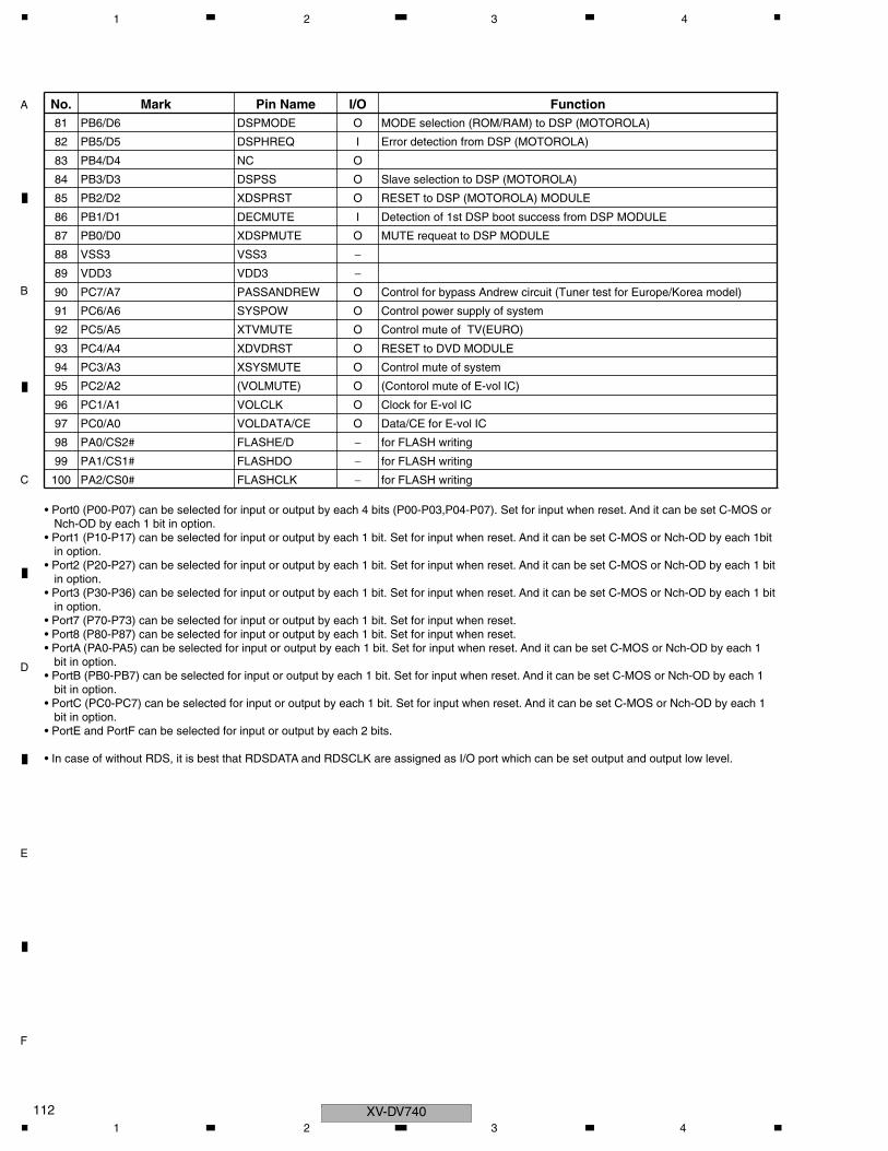
C
D
F
A
B
E
XV-DV740112
1 2 3 4
• Port0 (P00-P07) can be selected for input or output by each 4 bits (P00-P03,P04-P07). Set for input when reset. And it can be set C-MOS or Nch-OD by each 1 bit in option.• Port1 (P10-P17) can be selected for input or output by each 1 bit. Set for input when reset. And it can be set C-MOS or Nch-OD by each 1bit in option.• Port2 (P20-P27) can be selected for input or output by each 1 bit. Set for input when reset. And it can be set C-MOS or Nch-OD by each 1 bit in option.• Port3 (P30-P36) can be selected for input or output by each 1 bit. Set for input when reset. And it can be set C-MOS or Nch-OD by each 1 bit in option.• Port7 (P70-P73) can be selected for input or output by each 1 bit. Set for input when reset.• Port8 (P80-P87) can be selected for input or output by each 1 bit. Set for input when reset.• PortA (PA0-PA5) can be selected for input or output by each 1 bit. Set for input when reset. And it can be set C-MOS or Nch-OD by each 1 bit in option.• PortB (PB0-PB7) can be selected for input or output by each 1 bit. Set for input when reset. And it can be set C-MOS or Nch-OD by each 1 bit in option.• PortC (PC0-PC7) can be selected for input or output by each 1 bit. Set for input when reset. And it can be set C-MOS or Nch-OD by each 1 bit in option.• PortE and PortF can be selected for input or output by each 2 bits.
• In case of without RDS, it is best that RDSDATA and RDSCLK are assigned as I/O port which can be set output and output low level.
No. Mark Pin Name I/O Function81 PB6/D6 DSPMODE O MODE selection (ROM/RAM) to DSP (MOTOROLA)
82 PB5/D5 DSPHREQ I Error detection from DSP (MOTOROLA)
83 PB4/D4 NC O
84 PB3/D3 DSPSS O Slave selection to DSP (MOTOROLA)
85 PB2/D2 XDSPRST O RESET to DSP (MOTOROLA) MODULE
86 PB1/D1 DECMUTE I Detection of 1st DSP boot success from DSP MODULE
87 PB0/D0 XDSPMUTE O MUTE requeat to DSP MODULE
88 VSS3 VSS3 −89 VDD3 VDD3 −90 PC7/A7 PASSANDREW O Control for bypass Andrew circuit (Tuner test for Europe/Korea model)
91 PC6/A6 SYSPOW O Control power supply of system
92 PC5/A5 XTVMUTE O Control mute of TV(EURO)
93 PC4/A4 XDVDRST O RESET to DVD MODULE
94 PC3/A3 XSYSMUTE O Control mute of system
95 PC2/A2 (VOLMUTE) O (Contorol mute of E-vol IC)
96 PC1/A1 VOLCLK O Clock for E-vol IC
97 PC0/A0 VOLDATA/CE O Data/CE for E-vol IC
98 PA0/CS2# FLASHE/D − for FLASH writing
99 PA1/CS1# FLASHDO − for FLASH writing
100 PA2/CS0# FLASHCLK − for FLASH writing
1 2 3 4
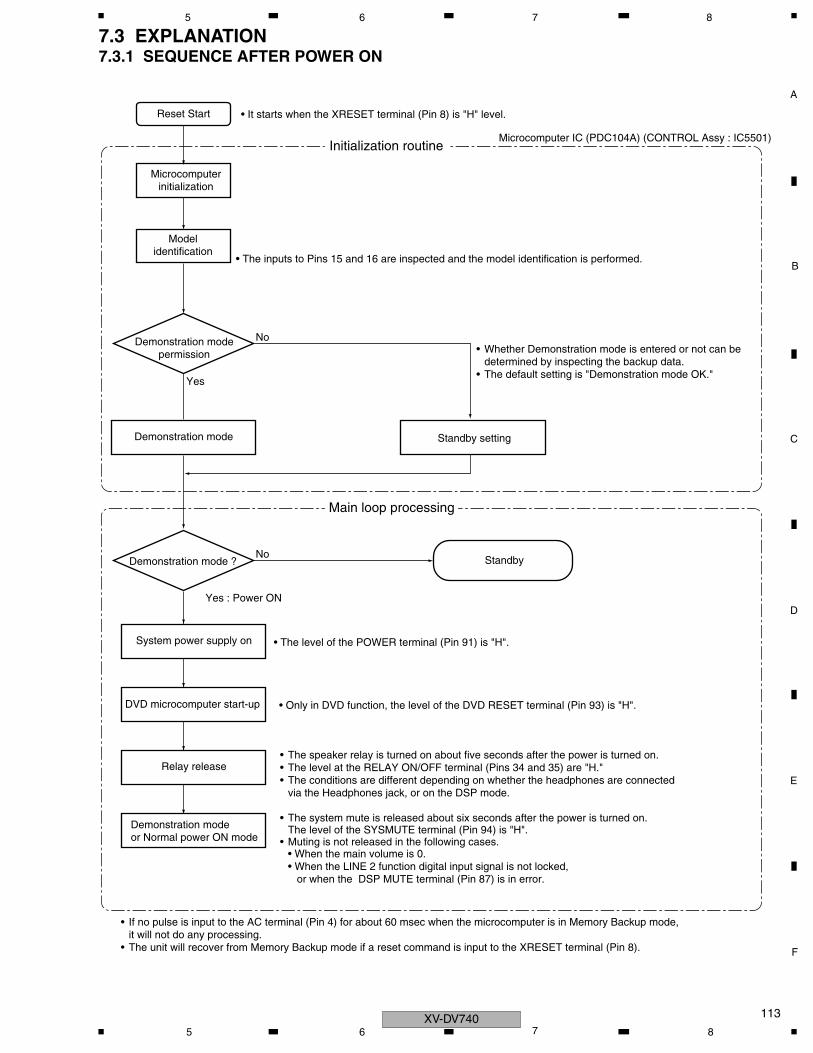
C
D
F
A
B
E
113
5 6 7 8
7.3 EXPLANATION7.3.1 SEQUENCE AFTER POWER ON
Reset Start
Demonstration mode ?
Yes : Power ON
Yes
No
No
Microcomputerinitialization
Modelidentification
Standby setting
• It starts when the XRESET terminal (Pin 8) is "H" level.
• The inputs to Pins 15 and 16 are inspected and the model identification is performed.
Demonstration modepermission
Demonstration mode
System power supply on
DVD microcomputer start-up
Relay release
Demonstration modeor Normal power ON mode
• The level of the POWER terminal (Pin 91) is "H".
• Only in DVD function, the level of the DVD RESET terminal (Pin 93) is "H".
• The speaker relay is turned on about five seconds after the power is turned on.• The level at the RELAY ON/OFF terminal (Pins 34 and 35) are "H."• The conditions are different depending on whether the headphones are connected
via the Headphones jack, or on the DSP mode.
• If no pulse is input to the AC terminal (Pin 4) for about 60 msec when the microcomputer is in Memory Backup mode, it will not do any processing.
• The unit will recover from Memory Backup mode if a reset command is input to the XRESET terminal (Pin 8).
• The system mute is released about six seconds after the power is turned on.The level of the SYSMUTE terminal (Pin 94) is "H".
• Muting is not released in the following cases.• When the main volume is 0.• When the LINE 2 function digital input signal is not locked, or when the DSP MUTE terminal (Pin 87) is in error.
• Whether Demonstration mode is entered or not can be determined by inspecting the backup data.
• The default setting is "Demonstration mode OK."
Standby
Initialization routine
Main loop processing
Microcomputer IC (PDC104A) (CONTROL Assy : IC5501)
XV-DV7405 6 7 8
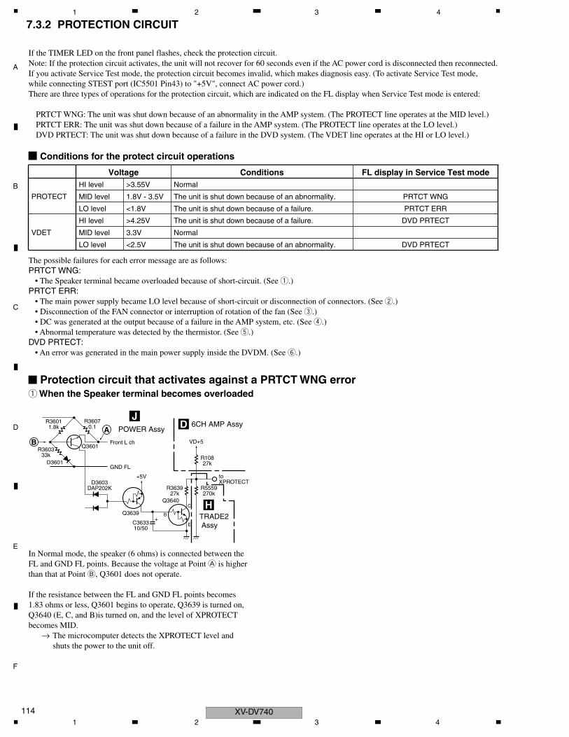
C
D
F
A
B
E
XV-DV740114
1 2 3 4
7.3.2 PROTECTION CIRCUIT
If the TIMER LED on the front panel flashes, check the protection circuit.Note: If the protection circuit activates, the unit will not recover for 60 seconds even if the AC power cord is disconnected then reconnected. If you activate Service Test mode, the protection circuit becomes invalid, which makes diagnosis easy. (To activate Service Test mode, while connecting STEST port (IC5501 Pin43) to "+5V", connect AC power cord.)There are three types of operations for the protection circuit, which are indicated on the FL display when Service Test mode is entered:
PRTCT WNG: The unit was shut down because of an abnormality in the AMP system. (The PROTECT line operates at the MID level.)PRTCT ERR: The unit was shut down because of a failure in the AMP system. (The PROTECT line operates at the LO level.)DVD PRTECT: The unit was shut down because of a failure in the DVD system. (The VDET line operates at the HI or LO level.)
Conditions for the protect circuit operations
Protection circuit that activates against a PRTCT WNG error
Voltage Conditions FL display in Service Test mode
PROTECT
HI level >3.55V Normal
MID level 1.8V - 3.5V The unit is shut down because of an abnormality. PRTCT WNG
LO level <1.8V The unit is shut down because of a failure. PRTCT ERR
VDET
HI level >4.25V The unit is shut down because of a failure. DVD PRTECT
MID level 3.3V Normal
LO level <2.5V The unit is shut down because of an abnormality. DVD PRTECT
The possible failures for each error message are as follows:PRTCT WNG:
• The Speaker terminal became overloaded because of short-circuit. (See 1.)PRTCT ERR:
• The main power supply became LO level because of short-circuit or disconnection of connectors. (See 2.)• Disconnection of the FAN connector or interruption of rotation of the fan (See 3.)• DC was generated at the output because of a failure in the AMP system, etc. (See 4.)• Abnormal temperature was detected by the thermistor. (See 5.)
DVD PRTECT:• An error was generated in the main power supply inside the DVDM. (See 6.)
1 When the Speaker terminal becomes overloaded
Q3601
Q3639
Q3640
B
E
C
+5VD3603
DAP202K
C363310/50
D3601
R36070.1
R363927k
R5559270k
R10827k
Front L ch
toXPROTECT
GND FL
R36011.8k
R360333k
B
A
VD+5
+
POWER Assy
J6CH AMP AssyD
TRADE2 Assy
H
In Normal mode, the speaker (6 ohms) is connected between the FL and GND FL points. Because the voltage at Point A is higher than that at Point B, Q3601 does not operate.
If the resistance between the FL and GND FL points becomes 1.83 ohms or less, Q3601 begins to operate, Q3639 is turned on, Q3640 (E, C, and B)is turned on, and the level of XPROTECT becomes MID.
→ The microcomputer detects the XPROTECT level and shuts the power to the unit off.
1 2 3 4
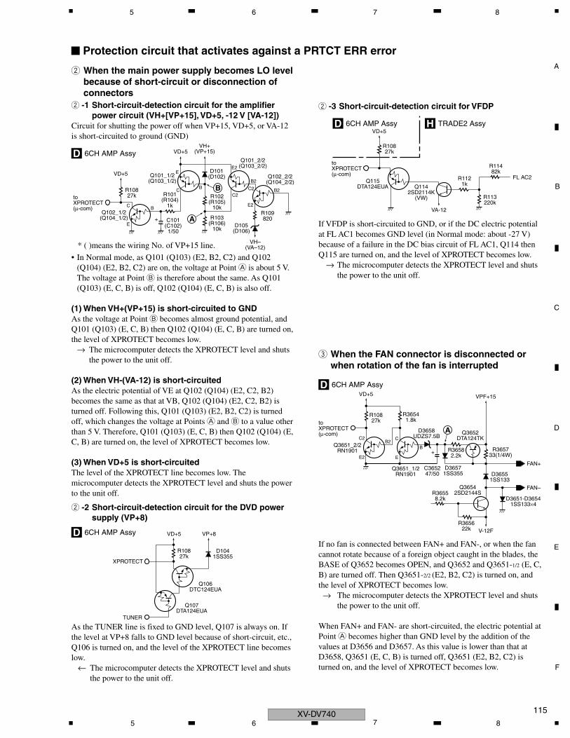
C
D
F
A
B
E
115
5 6 7 8
Protection circuit that activates against a PRTCT ERR error
B
A
A
C101(C102)1/50
+
+
toXPROTECT(µ-com)
6CH AMP AssyD
R10827k R101
(R104)1k
R102(R105)
10k
R103(R106)
10k
R109820
D105(D106)
Q102_1/2(Q104_1/2)
Q102_2/2(Q104_2/2)
Q101_1/2(Q103_1/2)
Q101_2/2(Q103_2/2)
D101(D102)VD+5
VD+5VH+
(VP+15)
VH–(VA–12)
2 -1 Short-circuit-detection circuit for the amplifier power circuit (VH+[VP+15], VD+5, -12 V [VA-12])
Circuit for shutting the power off when VP+15, VD+5, or VA-12 is short-circuited to ground (GND)
2 -3 Short-circuit-detection circuit for VFDP
2 -2 Short-circuit-detection circuit for the DVD power supply (VP+8)
XPROTECT
TUNER
6CH AMP AssyD VD+5
R10827k
D1041SS355
Q106DTC124EUA
Q107DTA124EUA
VP+8
• In Normal mode, as Q101 (Q103) (E2, B2, C2) and Q102 (Q104) (E2, B2, C2) are on, the voltage at Point A is about 5 V. The voltage at Point B is therefore about the same. As Q101 (Q103) (E, C, B) is off, Q102 (Q104) (E, C, B) is also off.
(1) When VH+(VP+15) is short-circuited to GNDAs the voltage at Point B becomes almost ground potential, and Q101 (Q103) (E, C, B) then Q102 (Q104) (E, C, B) are turned on, the level of XPROTECT becomes low.
→ The microcomputer detects the XPROTECT level and shuts the power to the unit off.
(2) When VH-(VA-12) is short-circuitedAs the electric potential of VE at Q102 (Q104) (E2, C2, B2) becomes the same as that at VB, Q102 (Q104) (E2, C2, B2) is turned off. Following this, Q101 (Q103) (E2, B2, C2) is turned off, which changes the voltage at Points A and B to a value other than 5 V. Therefore, Q101 (Q103) (E, C, B) then Q102 (Q104) (E, C, B) are turned on, the level of XPROTECT becomes low.
(3) When VD+5 is short-circuitedThe level of the XPROTECT line becomes low. The microcomputer detects the XPROTECT level and shuts the power to the unit off.
C
C
E
toXPROTECT(µ-com)
R10827k
R1121k
R113220k
R11482k
Q115DTA124EUA Q114
2SD2114K(VW)
VD+5
FL AC2
VA-12
E
B
BB2
B2
E2
E2
C2C2
As the TUNER line is fixed to GND level, Q107 is always on. If the level at VP+8 falls to GND level because of short-circuit, etc., Q106 is turned on, and the level of the XPROTECT line becomes low.
← The microcomputer detects the XPROTECT level and shuts the power to the unit off.
TRADE2 AssyH6CH AMP AssyD
toXPROTECT(µ-com)
R10827k
Q3651_2/2RN1901
Q3651_1/2RN1901
C2 C
E
B
E2
B2
VD+5
FAN+
VPF+15
V-12F
R36541.8k
D3658UDZS7.5B
D36571SS355 D3655
1SS133
D3651-D36541SS133×4
R36558.2k
R365622k
R36582.2k
R365733(1/4W)
Q3652DTA124TK
Q36542SD2144S
C365247/50
6CH AMP AssyD
If VFDP is short-circuited to GND, or if the DC electric potential at FL AC1 becomes GND level (in Normal mode: about -27 V) because of a failure in the DC bias circuit of FL AC1, Q114 then Q115 are turned on, and the level of XPROTECT becomes low.
→ The microcomputer detects the XPROTECT level and shuts the power to the unit off.
2 When the main power supply becomes LO level because of short-circuit or disconnection of connectors
3 When the FAN connector is disconnected or when rotation of the fan is interrupted
FAN–
If no fan is connected between FAN+ and FAN-, or when the fan cannot rotate because of a foreign object caught in the blades, the BASE of Q3652 becomes OPEN, and Q3652 and Q3651-1/2 (E, C, B) are turned off. Then Q3651-2/2 (E2, B2, C2) is turned on, and the level of XPROTECT becomes low. → The microcomputer detects the XPROTECT level and shuts
the power to the unit off.
When FAN+ and FAN- are short-circuited, the electric potential at Point A becomes higher than GND level by the addition of the values at D3656 and D3657. As this value is lower than that at D3658, Q3651 (E, C, B) is turned off, Q3651 (E2, B2, C2) is turned on, and the level of XPROTECT becomes low.
* ( )means the wiring No. of VP+15 line.
XV-DV7405 6 7 8
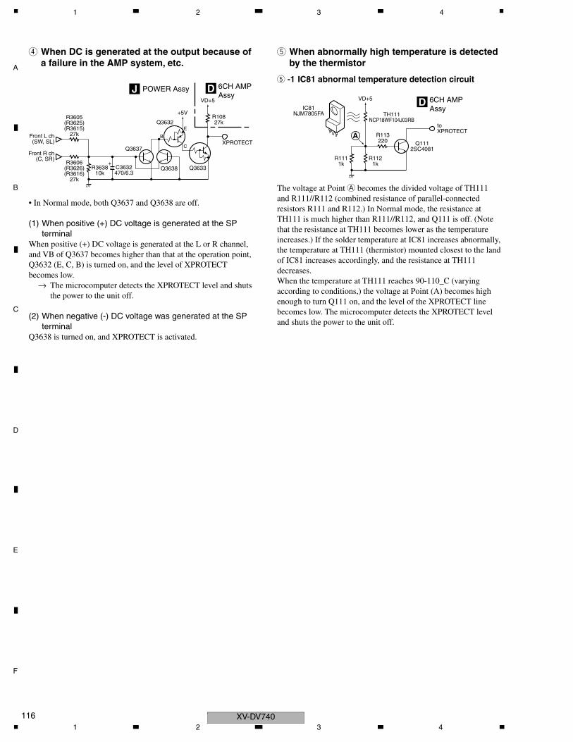
C
D
F
A
B
E
XV-DV740116
1 2 3 4
4 When DC is generated at the output because of a failure in the AMP system, etc.
5 When abnormally high temperature is detected by the thermistor
R3605(R3625)(R3615)
27k
R3606(R3626)(R3616)
27k
R363810k
Front L ch(SW, SL)
+5V
C3632470/6.3
Q3637Q111
2SC4081
R113220
IC81NJM7805FA
R1121k
TH111NCP18WF104J03RB
R1111k
Q3638
Q3632
Q3633
B
C
E
+
XPROTECT
toXPROTECT
POWER AssyJ
R10827k
VD+5 VD+5
6CH AMP Assy
D6CH AMP Assy
D
Front R ch(C, SR)
• In Normal mode, both Q3637 and Q3638 are off.
(1) When positive (+) DC voltage is generated at the SP terminal
When positive (+) DC voltage is generated at the L or R channel, and VB of Q3637 becomes higher than that at the operation point, Q3632 (E, C, B) is turned on, and the level of XPROTECT becomes low.
→ The microcomputer detects the XPROTECT level and shuts the power to the unit off.
(2) When negative (-) DC voltage was generated at the SP terminal
Q3638 is turned on, and XPROTECT is activated.
5 -1 IC81 abnormal temperature detection circuit
A
The voltage at Point A becomes the divided voltage of TH111 and R111//R112 (combined resistance of parallel-connected resistors R111 and R112.) In Normal mode, the resistance at TH111 is much higher than R111//R112, and Q111 is off. (Note that the resistance at TH111 becomes lower as the temperature increases.) If the solder temperature at IC81 increases abnormally, the temperature at TH111 (thermistor) mounted closest to the land of IC81 increases accordingly, and the resistance at TH111 decreases.When the temperature at TH111 reaches 90-110_C (varying according to conditions,) the voltage at Point (A) becomes high enough to turn Q111 on, and the level of the XPROTECT line becomes low. The microcomputer detects the XPROTECT level and shuts the power to the unit off.
1 2 3 4
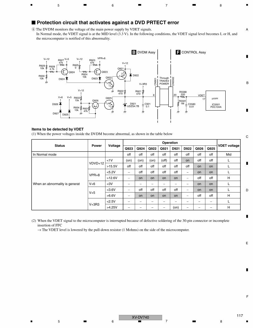
C
D
F
A
B
E
117
5 6 7 8
Protection circuit that activates against a DVD PRTECT error6 The DVDM monitors the voltage of the main power supply by VDET signals. In Normal mode, the VDET signal is at the MID level (3.3 V). In the following conditions, the VDET signal level becomes L or H, and the microcomputer is notified of this abnormality.
DVDM AssyB CONTROL AssyF
R92910k
R93010k
R9284.7k
R92747k
Q924 Q923
R922470
D922D923D924
IC5501PDC104A
Q922
Q925
D925D927
D926 D921UDZS4.7B
Q926
Q921
V+5V+12
R921470
R55911M
R5588220
C9210.1
V+3R3
R93315k
R93410k
V+12
V+5V+6
R9250
R92410k
R92347k
VPR+8V+12
V+12
R93147k
C55800.01
17
208 VDET
ThroughTRADE2POWER C
N55
02
CN
901
µcom
Items to be detected by VDET(1) When the power voltages inside the DVDM become abnormal, as shown in the table below
(2) When the VDET signal to the microcomputer is interrupted because of defective soldering of the 30-pin connector or incomplete insertion of FFC→ The VDET level is lowered by the pull-down resistor (1 Mohms) on the side of the microcomputer.
Status Power VoltageOperation
VDET voltageQ923 Q924 Q922 Q921 D921 D922 Q926 Q925
In Normal mode off off off off off off off off Mid
When an abnormality is generat
VDVD+12<1V (on) (on) (on) (off) off on off off L
>15.5V off off off off off off on on L
VPR+8<5.2V − off off off off − on on L
>12.6V − on on on on − off off H
V+6 <3V − − − − − − on on L
V+5<3.6V − off off off off − on on L
>6.6V − on on on on − off off H
V+3R3<2.5V − − − − − − − − L
>4.25V − − − − (on) − − − H
XV-DV7405 6 7 8
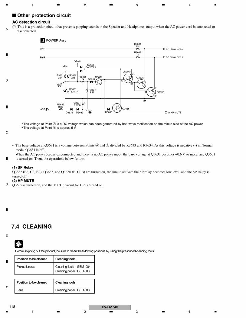
C
D
F
A
B
E
XV-DV740118
1 2 3 4
7.4 CLEANING
• The base voltage at Q3631 is a voltage between Points A and B divided by R3633 and R3634. As this voltage is negative (-) in Normal mode, Q3631 is off.When the AC power cord is disconnected and there is no AC power input, the base voltage at Q3631 becomes +0.6 V or more, and Q3631 is turned on. Then, the operations below follow.
(1) SP RelayQ3632 (E2, C2, B2), Q3633, and Q3636 (E, C, B) are turned on, the line to activate the SP relay becomes low level, and the SP Relay is turned off.(2) HP MUTEQ3635 is turned on, and the MUTE circuit for HP is turned on.
Other protection circuitAC detection circuit7 This is a protection circuit that prevents popping sounds in the Speaker and Headphones output when the AC power cord is connected or disconnected.
POWER AssyJ
• The voltage at Point A is a DC voltage which has been generated by half-wave rectification on the minus side of the AC power.• The voltage at Point B is approx. 5 V.
Q3633
Q3636
Q3632
Q3635
Q3631
D3636
D3634
R36344.7k
R363310k
D3635DAN202K
R364110k
B
C
C2B2
E2
E
+
RYF to SP Relay Circuit
to SP Relay Circuit
to HP MUTE
VD+5
VH+
R363233k
R363133k
R36421k
RYR
ACB
B
A
D3631MTZJ5.1A
D3633D3632
C36312.2/50R3635
3.3k
Before shipping out the product, be sure to clean the following positions by using the prescribed cleaning tools:
Position to be cleaned Cleaning tools
Pickup lenses Cleaning liquid : GEM1004Cleaning paper : GED-008
Position to be cleaned Cleaning tools
Fans Cleaning paper : GED-008
1 2 3 4
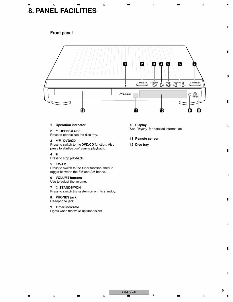
C
D
F
A
B
E
119
5 6 7 8
8. PANEL FACILITIES
Front panel
1 Operation indicator
2 OPEN/CLOSEPress to open/close the disc tray.
3 DVD/CDPress to switch to the DVD/CD function. Also press to start/pause/resume playback.
4Press to stop playback.
5 FM/AMPress to switch to the tuner function, then to toggle between the FM and AM bands.
6 VOLUME buttonsUse to adjust the volume.
7 STANDBY/ONPress to switch the system on or into standby.
8 PHONES jackHeadphone jack.
9 Timer indicator Lights when the wake-up timer is set.
10 DisplaySee Display for detailed information.
11 Remote sensor
12 Disc tray
PHONES
6 DVD/CD0 OPEN/CLOSE FM/AM VOL.– DOWN UP +7 STANDBY/ON
1 3 4 5 6 7
9101112 8
2
7
6
0
XV-DV7405 6 7 8
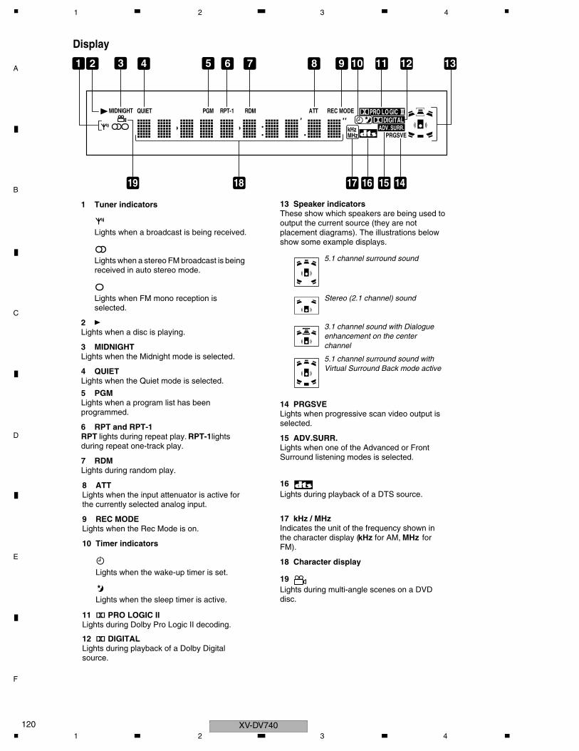
C
D
F
A
B
E
XV-DV740120
1 2 3 4
Display
1 Tuner indicators
Lights when a broadcast is being received.
Lights when a stereo FM broadcast is being received in auto stereo mode.
Lights when FM mono reception is selected.
2Lights when a disc is playing.
3 MIDNIGHTLights when the Midnight mode is selected.
4 QUIETLights when the Quiet mode is selected.
5 PGMLights when a program list has been programmed.
6 RPT and RPT-1 RPT lights during repeat play. RPT-1 lights during repeat one-track play.
7 RDM Lights during random play.
8 ATT Lights when the input attenuator is active for the currently selected analog input.
9 REC MODE Lights when the Rec Mode is on.
10 Timer indicators
Lights when the wake-up timer is set.
Lights when the sleep timer is active.
11 2 PRO LOGIC II Lights during Dolby Pro Logic II decoding.
12 2 DIGITAL Lights during playback of a Dolby Digital source.
MIDNIGHT QUIET PGM RPT- 1 RDM ATT REC MODE
kHz ADV. SURR.PRGSVE
DIGITAL
MHz
PRO LOGIC
15 1416171819
21 3 4 5 6 7 8 9 10 11 12 13
3
13 Speaker indicatorsThese show which speakers are being used to output the current source (they are not placement diagrams). The illustrations below show some example displays.
14 PRGSVELights when progressive scan video output is selected.
15 ADV.SURR. Lights when one of the Advanced or Front Surround listening modes is selected.
16Lights during playback of a DTS source.
17 kHz / MHzIndicates the unit of the frequency shown in the character display (kHz for AM, MHz for FM).
18 Character display
19Lights during multi-angle scenes on a DVD disc.
5.1 channel surround sound
Stereo (2.1 channel) sound
3.1 channel sound with Dialogue enhancement on the center channel
5.1 channel surround sound with Virtual Surround Back mode active
1 2 3 4
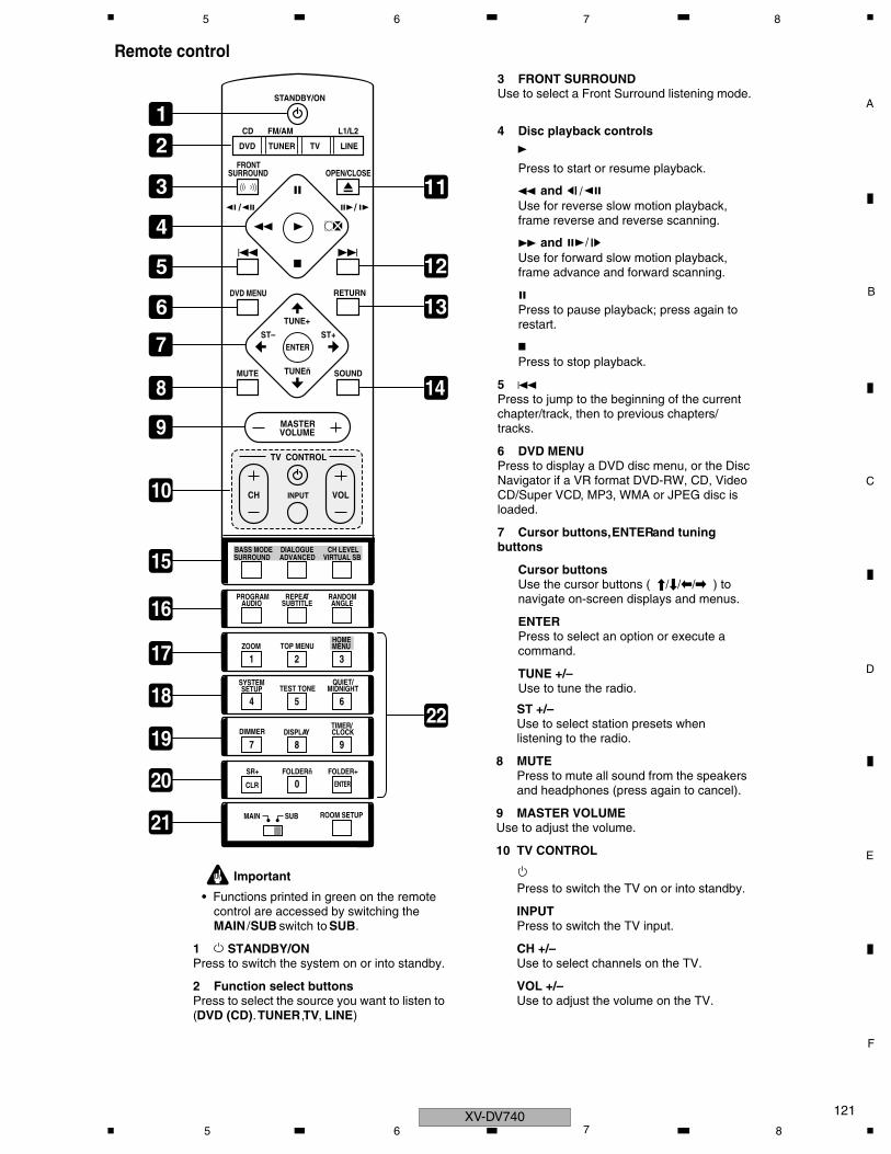
C
D
F
A
B
E
121
5 6 7 8
Remote control
Important
• Functions printed in green on the remote control are accessed by switching the MAIN /SUB switch to SUB.
1 STANDBY/ON Press to switch the system on or into standby.
2 Function select buttonsPress to select the source you want to listen to (DVD (CD). TUNER, TV, LINE)
ST+
TUNE+
ENTER
TUNEñ
MASTERVOLUME
ST–
STANDBY/ON
CD FM/AM
OPEN/CLOSE
DVD TUNER TV LINE
L1/L2
1
4 4
°
8
3
7
0
DVD MENU RETURN
SOUND
TV CONTROL
CH VOLINPUT
MUTE
TEST TONE
1 2 3ZOOM TOP MENU
DIMMER
REPEATAUDIO ANGLE
RANDOMSUBTITLE
PROGRAM
4 5 6
7 8 9
0
MAIN SUB
FOLDERñ
ROOM SETUP
CLR ENTER
FOLDER+SR+
MENUHOME
SETUPSYSTEM
DISPLAY CLOCKTIMER/
BASS MODE DIALOGUE CH LEVELSURROUND ADVANCED VIRTUAL SB
FRONTSURROUND
MIDNIGHTQUIET/
1
2
3
4
5
6
7
8
9
10
15
16
17
18
19
21
20
11
12
13
14
22
3 FRONT SURROUNDUse to select a Front Surround listening mode.
4 Disc playback controls
Press to start or resume playback.
Use for reverse slow motion playback, frame reverse and reverse scanning.
Use for forward slow motion playback, frame advance and forward scanning.
Press to pause playback; press again to restart.
Press to stop playback.
5Press to jump to the beginning of the current chapter/track, then to previous chapters/tracks.
6 DVD MENUPress to display a DVD disc menu, or the Disc Navigator if a VR format DVD-RW, CD, Video CD/Super VCD, MP3, WMA or JPEG disc is loaded.
7 Cursor buttons, ENTER and tuning buttons
Cursor buttonsUse the cursor buttons ( ) to navigate on-screen displays and menus.
ENTERPress to select an option or execute a command.
TUNE +/–Use to tune the radio.
3
¡ 0E/ and
/¡ 0 E and
7
8
4
»/«/|/\
ST +/–Use to select station presets when listening to the radio.
8 MUTE Press to mute all sound from the speakers and headphones (press again to cancel).
9 MASTER VOLUMEUse to adjust the volume.
10 TV CONTROL
Press to switch the TV on or into standby.
INPUTPress to switch the TV input.
CH +/–Use to select channels on the TV.
VOL +/–Use to adjust the volume on the TV.
XV-DV7405 6 7 8
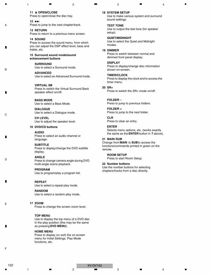
C
D
F
A
B
E
XV-DV740122
1 2 3 4
11 OPEN/CLOSEPress to open/close the disc tray.
12Press to jump to the next chapter/track.
13 RETURNPress to return to a previous menu screen.
14 SOUNDPress to access the sound menu, from which you can adjust the DSP effect level, bass and treble, etc.
15 Surround sound mode/sound enhancement buttons
SURROUND Use to select a Surround mode.
ADVANCED Use to select an Advanced Surround mode.
VIRTUAL SB Press to switch the Virtual Surround Back speaker effect on/off.
0
¢
BASS MODE Use to select a Bass Mode.
DIALOGUE Use to select a Dialogue mode.
CH LEVEL Use to adjust the speaker level.
16 DVD/CD buttons
AUDIO Press to select an audio channel or language.
SUBTITLE Press to display/change the DVD subtitle display.
ANGLE Press to change camera angle during DVD multi-angle scene playback .
PROGRAM Use to program/play a program list.
REPEAT Use to select a repeat play mode.
RANDOM Use to select a random play mode.
17 ZOOM Press to change the screen zoom level.
TOP MENUUse to display the top menu of a DVD disc in the play position (this may be the same as pressing DVD MENU).
HOME MENUPress to display (or exit) the on-screen menu for Initial Settings, Play Mode functions, etc.
18 SYSTEM SETUPUse to make various system and surround sound settings.
TEST TONE Use to output the test tone (for speaker setup).
QUIET/MIDNIGHTUse to select the Quiet and Midnight modes.
19 DIMMERPress to switch between normal and dimmed front panel display.
DISPLAYPress to display/change disc information shown on-screen .
TIMER/CLOCK Press to display the clock and to access the timer menu.
20 SR+Press to switch the SR+ mode on/off.
FOLDER –Press to jump to previous folders.
FOLDER +Press to jump to the next folder.
CLRPress to clear an entry.
ENTERSelects menu options, etc. (works exactly the same as the ENTER button in 7 above).
21 MAIN /SUBChange from MAIN to SUB to access the functions/commands printed in green on the remote.
ROOM SETUP Press to start Room Setup.
22 Number buttonsUse the number buttons for selecting chapters/tracks from a disc directly.
1 2 3 4
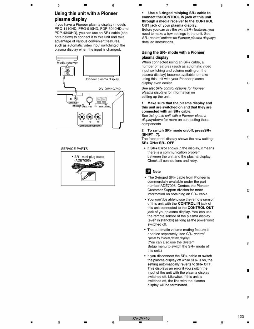
C
D
F
A
B
E
123
5 6 7 8
Using this unit with a Pioneer plasma displayIf you have a Pioneer plasma display (models PRO-1110HD, PRO-910HD, PDP-5040HD and PDP-4340HD), you can use an SR+ cable (see note below) to connect it to this unit and take advantage of various convenient features, such as automatic video input switching of the plasma display when the input is changed.
• Use a 3-ringed miniplug SR+ cable to connect the CONTROL IN jack of this unit through a media receiver to the CONTROL OUT jack of your plasma display.Before you can use the extra SR+ features, you need to make a few settings in the unit. See SR+ control options for Pioneer plasma displays detailed instructions.
AM LOOP ANTENNA
FMUNBAL 75 Ω
IN
ANTENNACONTROL
COMPONENT VIDEO OUT
PRPBY
OUT
CONTROL
Pioneer plasma display
XV-DV440/740
Media receiver
Using the SR+ mode with a Pioneer plasma displayWhen connected using an SR+ cable, a number of features (such as automatic video input switching and volume muting on the plasma display) become available to make using this unit with your Pioneer plasma display even easier.
See also SR+ control options for Pioneer plasma displays for information on setting up the unit.
1 Make sure that the plasma display and this unit are switched on and that they are connected with an SR+ cable.See Using this unit with a Pioneer plasma display above for more on connecting these components.
2 To switch SR+ mode on/off, press SR+ (SHIFT + 7).The front panel display shows the new setting; SR+ ON or SR+ OFF.
• If SR+ Error shows in the display, it means there is a communication problem between the unit and the plasma display. Check all connections and retry.
Note
• The 3-ringed SR+ cable from Pioneer is commercially available under the part number ADE7095. Contact the Pioneer Customer Support division for more information on obtaining an SR+ cable.
• You won't be able to use the remote sensor of this unit with the CONTROL IN jack of this unit connected to the CONTROL OUT jack of your plasma display. You can use the remote sensor of the plasma display (even in standby) as long as the power isnít switched off.
• The automatic volume muting feature is enabled separately; see SR+ control options for Pioneer plasma displays.(You can also use the System Setup menu to switch the SR+ mode of this unit.)
• If you disconnect the SR+ cable or switch the plasma display off while SR+ is on, the setting automatically reverts to SR+ OFF. This displays an error if you switch the input of the unit with the plasma display switched off. Likewise, if this unit is switched off, the link with the plasma display will be terminated.
• SR+ mini-plug cable(ADE7095)
SERVICE PARTS
XV-DV7405 6 7 8
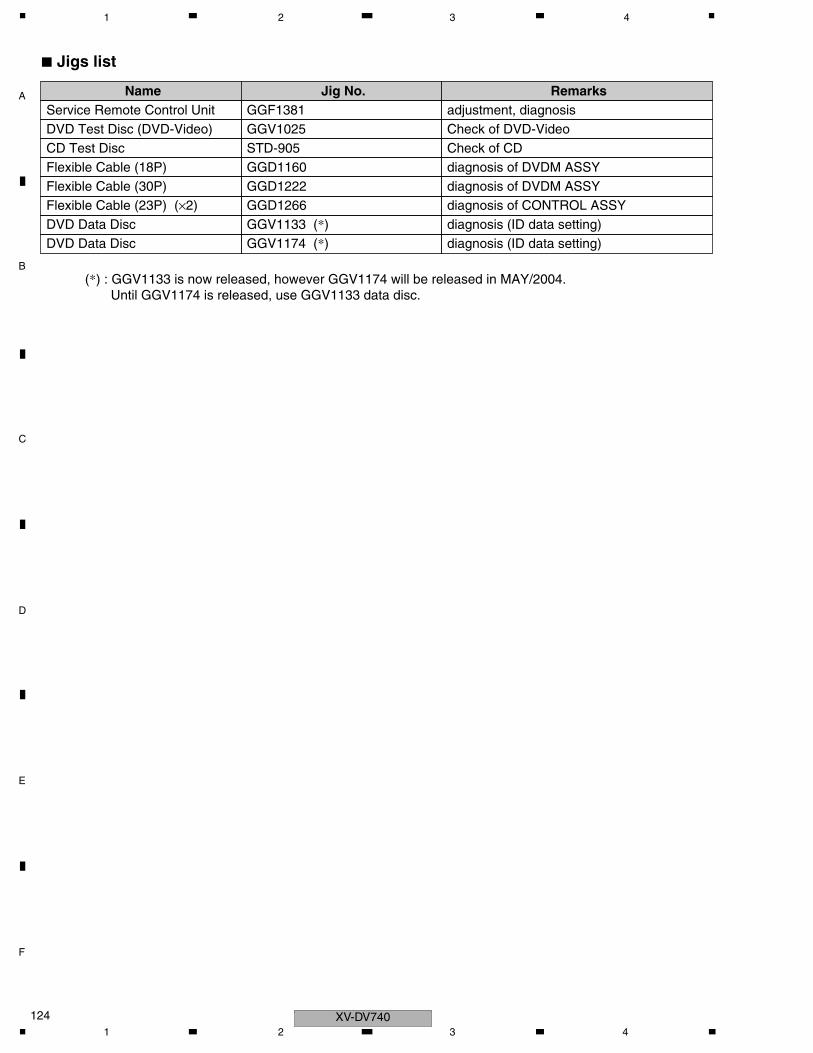
C
D
F
A
B
E
XV-DV740124
1 2 3 4
Service Remote Control Unit GGF1381DVD Test Disc (DVD-Video) GGV1025
adjustment, diagnosisName Jig No. Remarks
Check of DVD-VideoCD Test Disc STD-905 Check of CDFlexible Cable (18P) GGD1160Flexible Cable (30P) GGD1222
diagnosis of DVDM ASSYdiagnosis of DVDM ASSY
Flexible Cable (23P) (×2) GGD1266 diagnosis of CONTROL ASSYDVD Data Disc GGV1133 (*)DVD Data Disc GGV1174 (*)
diagnosis (ID data setting)diagnosis (ID data setting)
7 Jigs list
(*) : GGV1133 is now released, however GGV1174 will be released in MAY/2004. Until GGV1174 is released, use GGV1133 data disc.
1 2 3 4