Embed Size (px)
Citation preview
Xilinx Answer 58495 – PCI-Express Interrupt Debugging Guide 1
Xilinx Answer 58495
Xilinx PCI Express Interrupt Debugging Guide
Important Note: This downloadable PDF of an Answer Record is provided to enhance its usability and readability. It is important to note that Answer Records are Web-based content that are frequently updated as new information becomes available. You are reminded to visit the Xilinx Technical Support Website and review (Xilinx Answer 58495) for the latest version of this Answer.
Introduction
PCI Express hardblocks from Xilinx have access to three different types of interrupts: Legacy Interrupt, MSI (Message Signaled Interrupts) or MSI-X depending on their design requirements. This document discusses different aspects of PCI Express interrupts to successfully get interrupts working in a PCI Express design. Details on how to generate Legacy Interrupt and Message Signal Interrupts (MSI) can be found in the respective product guides of the Xilinx PCI Express cores. The general principal for properly generating interrupts is same for all cores but it is slightly different in Virtex-7 FPGA Gen3 Integrated Block for PCI Express core. This is discussed in detail in this document with simulation waveforms and testbench.
Interrupt Types in PCI Express
There are three interrupt types in PCI Express. They are as follows:
1. Legacy Interrupts 2. MSI Interrupts 3. MSI-X Interrupts
Legacy Interrupts
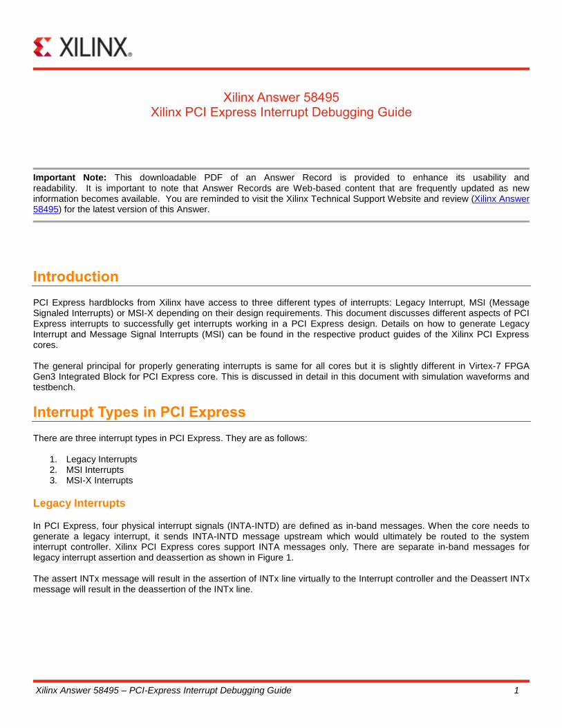
In PCI Express, four physical interrupt signals (INTA-INTD) are defined as in-band messages. When the core needs to generate a legacy interrupt, it sends INTA-INTD message upstream which would ultimately be routed to the system interrupt controller. Xilinx PCI Express cores support INTA messages only. There are separate in-band messages for legacy interrupt assertion and deassertion as shown in Figure 1. The assert INTx message will result in the assertion of INTx line virtually to the Interrupt controller and the Deassert INTx message will result in the deassertion of the INTx line.
Xilinx Answer 58495 – PCI-Express Interrupt Debugging Guide 2
Figure 1 - Assert-Deassert INTx Messages
Legacy Interrupt Assertion
When a Legacy device delivers an Assert_INTx message, it also sets its Interrupt Pending bit located in memory or I/O space and also sets the Interrupt Pending bit located within the Configuration Status register. Figure 2 shows a snap shot of the interrupt status register.
Figure 2 : Interrupt status register

Xilinx Answer 58495 – PCI-Express Interrupt Debugging Guide 3
MSI Interrupts
All MSI capable devices implement the MSI capability structure defined in the PCI Local Bus Specification v3.0.
Figure 3 - 32-bit MSI Capability Structure
PCI and PCI Express devices that enable MSI send interrupts to the CPU in-band. A MSI enabled device will interrupt the CPU by writing to a specific address in memory with a payload of 1 DW (double word). Figure 4 below breaks down the contents of a MSI interrupt.
Figure 4 - MSI Interrupt Packet Contents
The memory write address combined with the data field allows a device to generate multiple unique interrupts. A memory write with an exclusive address and data field is commonly referred to as a MSI vector. The device may support 1, 2, 4, 8, 16, or 32 interrupt vectors. A device indicates how many vectors it supports through the Multiple Message Capable field within the Message Control Register. The address of the Memory Write is loaded from the Message Address field and the data payload signifies the MSI vector to be sent. The number of MSI vectors allocated to the device determines what bits in the lower sixteen are writable. For example, a device which has eight vectors allocated will only be able to modify the lower three bits of message data. Three writable bits allows the device to send 8 unique MSI interrupt vectors upstream.
Advantages of MSI
There are a number of advantages when employing MSI interrupts rather than legacy interrupts. Each of the main advantages is explained below.
Xilinx Answer 58495 – PCI-Express Interrupt Debugging Guide 4
Removal of IRQ Sharing As the number of peripherals in a system has sky rocketed, devices generating legacy interrupts commonly have to share IRQ numbers. When an interrupt is issued targeting a shared IRQ number, the processor will sequentially call every device service routine associated with that IRQ. Each service routine will check its devices state and service any pending interrupt. Devices implementing MSI interrupts have at least one unique address associated to it which removes the need for interrupt sharing and performance degradation associated with device polling. Latency Reduction and Multiple Interrupts In legacy interrupt implementations, an interrupt handler typically reads its peripheral’s internal device registers to ident ify why the device has signaled an interrupt. The process of identifying why the device has interrupted adds additional overhead to the handling of the interrupt. The inclusion of multiple MSI vectors allows a device to provide more information when interrupting. A vector provides the reason for interrupting and removes the need for costly device accesses. This feature essentially moves the first round of decision making into hardware, thus simplifying the interrupt handler within the device driver. Mechanical Reduction and Race Conditions As stated above, MSI interrupts are sent “in band” and do not require additional pins or board traces. This allows for a simpler and cheaper board design. In addition to simpler board design, the elimination of out of band interrupts also prevents a common legacy race condition. Interrupts are commonly used to signal the device handler that a data transfer has completed. Assume that the peripheral sends out the final data block followed by the assertion of INTA to signal data transfer completion. Due to the parallel nature of these two events, it is possible the interrupt becomes visible to the CPU before the data transfer has completed. This race condition could result in stale data being read by the device handler. MSI resolves this issue because the interrupt is sent “in band” and will only be processed after all data has been transferred.
MSI Example
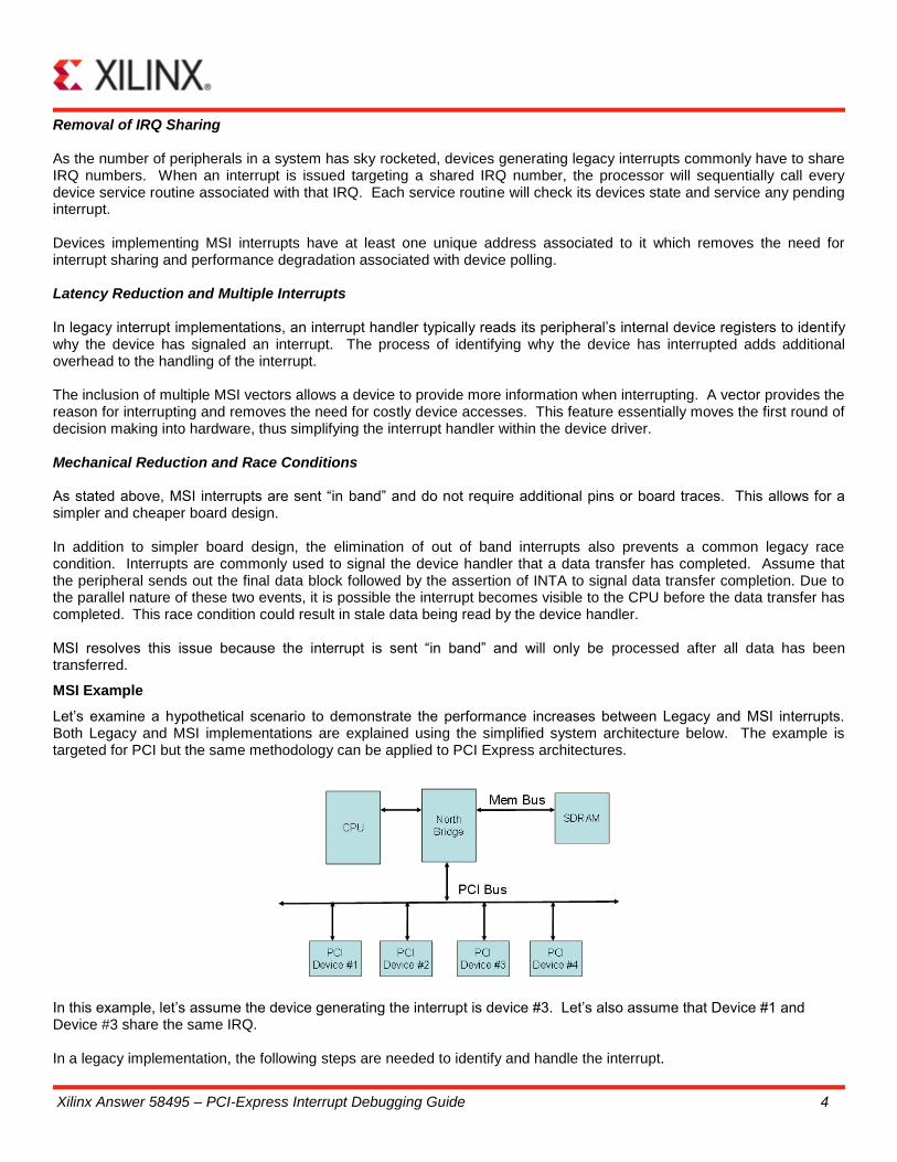
Let’s examine a hypothetical scenario to demonstrate the performance increases between Legacy and MSI interrupts. Both Legacy and MSI implementations are explained using the simplified system architecture below. The example is targeted for PCI but the same methodology can be applied to PCI Express architectures.
In this example, let’s assume the device generating the interrupt is device #3. Let’s also assume that Device #1 and Device #3 share the same IRQ. In a legacy implementation, the following steps are needed to identify and handle the interrupt.

Xilinx Answer 58495 – PCI-Express Interrupt Debugging Guide 5
1) Device generates Legacy interrupt by asserting one of its INT# pins 2) CPU acknowledges interrupt and polls Device #1 by calling its ISR (Interrupt Service Routine). 3) CPU polls Device #3 by calling its ISR. The ISR sees that its device has interrupted and reads the devices
internal registers to identify the cause of the issue. 4) ISR takes action to service the device.
In an implementation using MSI, the following typically occur. 1) Device generates interrupt by sending MSI Memory Write upstream 2) CPU acknowledges interrupt and calls Device #3 ISR. The handler already knows why the device interrupted
based on the MSI vector. 3) ISR takes action to service the device.
In this example, the MSI implementation reduces the total time servicing the interrupt by one device access.
Configuring MSI
Similar to many of the PCI Express capabilities, the MSI capability structure contains both capabilities and control field. These fields operate as a handshake between the device capability and system capability. Software is ultimately responsible for enabling MSI support within a device. Software is also responsible for enabling multiple MSI vectors by writing to the Multiple Message Enable field within the MSI Control register. Investigation shows SW distributions may only support a limited number of vectors per device, while some distributions may not contain any multi-vector support. Therefore, it is important that the chosen chipset and system software meets the MSI requirements for the targeted device. When the enumeration software scans a system and discovers MSI capability structure in an endpoint in the system, it reads the Multiple Message Capable field in the endpoint's Message Control Register to determine how many MSI interrupts the endpoint supports. Depending on the value read from this field the software writes a value that is equal to or lesser than the value read from the Multiple Message Capable field into the Multiple Message Enable Field. In the next step, the software writes the Message Data into the endpoint's Message Data Register field and also writes memory address to the Message Address Register. This is the address which goes into the MSI address header field. After this, the software enables MSI by setting MSI enable bit in the endpoint's Message control register. This will enable MSI as the only interrupt delivery option. Once the Endpoint device wants to generate the MSI interrupt, it generates a write request to the address specified in the message address register with the data contents specified in the message data register.
Figure 5: 32- bit MSI capability register set format

Xilinx Answer 58495 – PCI-Express Interrupt Debugging Guide 6
Figure 6: Fields in MSI Control Register
When debugging MSI issues, make sure the integrity of the MSI packet is correct as described below.
o Lower 16 bits of the data payload and the address fields in the MSI packet header comes from the values programmed in the MSI capability register; make sure the corresponding values match.
o MSI is a single DW transaction so the last BE field must be 0000b and length field must be 01h. o First BE filed must be 1111b. o The attribute bits for No Snoop and Relaxed Ordering must be zero.
Setting up MSI
The first consideration when implementing MSI is to determine the number of supported vectors. The number of MSI vectors is user configurable while customizing the endpoint solution. The number of vectors selected is translated directly to the Multiple Message Capable field within the MSI Control register. Figure 7 show the MSI setup GUI for Virtex-7 FPAG Gen3 Integrated Block for PCI Express cores respectively.
Figure 7 – Virtex-7 FPGA Gen3 Integrated PCIe Block MSI Vector Configuration
MSI implementation
After customizing the solution with MSI support, the application must be able to generate MSI interrupts. The generation of a MSI interrupt by the backend application is simplified using the Endpoints Configuration (CFG) interface. The interface allows the user to generate a MSI interrupt targeting a specific vector by editing the contents of the MESSAGE_DATA field.
Xilinx Answer 58495 – PCI-Express Interrupt Debugging Guide 7
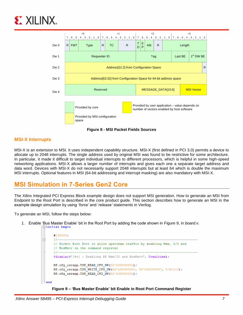
R FMT Type R
Requester ID
Address[31:2] from Configuration Space R
RT
DR Length
Tag Last BE 1st DW BE
Address[63:32] from Configuration Space for 64-bit address space
+2 +3+0
7 6 5 4 3 2 1 0 7 6 5 4 3 2 1 0 7 6 5 4 3 2 1 0 7 6 5 4 3 2 1 0
+1
TCE
PAttr
Reserved MESSAGE_DATA[15:6] MSI Vector
Provided by core
Provided by MSI configuration
space
Provided by user application – value depends on
number of vectors enabled by host software
Dw 0
Dw 1
Dw 2
Dw 3
Dw 4
Figure 8 - MSI Packet Fields Sources
MSI-X Interrupts
MSI-X is an extension to MSI. It uses independent capability structure. MSI-X (first defined in PCI 3.0) permits a device to allocate up to 2048 interrupts. The single address used by original MSI was found to be restrictive for some architecture. In particular, it made it difficult to target individual interrupts to different processors, which is helpful in some high-speed networking applications. MSI-X allows a larger number of interrupts and gives each one a separate target address and data word. Devices with MSI-X do not necessarily support 2048 interrupts but at least 64 which is double the maximum MSI interrupts. Optional features in MSI (64-bit addressing and interrupt masking) are also mandatory with MSI-X.
MSI Simulation in 7-Series Gen2 Core
The Xilinx Integrated PCI Express Block example design does not support MSI generation. How to generate an MSI from Endpoint to the Root Port is described in the core product guide. This section describes how to generate an MSI in the example design simulation by using ‘force’ and ‘release’ statements in Verilog. To generate an MSI, follow the steps below:
1. Enable ‘Bus Master Enable’ bit in the Root Port by adding the code shown in Figure 9, in board.v.
Figure 9 – ‘Bus Master Enable’ bit Enable in Root Port Command Register

Xilinx Answer 58495 – PCI-Express Interrupt Debugging Guide 8
2. In dsport/pci_exp_usrapp_tx.v, add the following to enable Bus Master Enable bit in the Endpoint Command
Register.
3. Add the following in dsport/pci_exp_usrapp_tx.v to configure the MSI registers.
4. Figure 10 shows interface waveform for requesting interrupt service from the user application to the core. Users should assert cfg_interrupt and provide the Message data on cfg_interrupt_di as shown in the waveform. A detailed information on generating an MSI interrupt request can be found in PG054 .
Figure 10 – Requesting Interrupt Service (PG054)
In order to generate an MSI, assert cfg_interrupt and provide Message data on cfg_interrupt_di. This can be done by using verilog force-release statements as shown in Figure 11. Add the following code snippet to board.v.
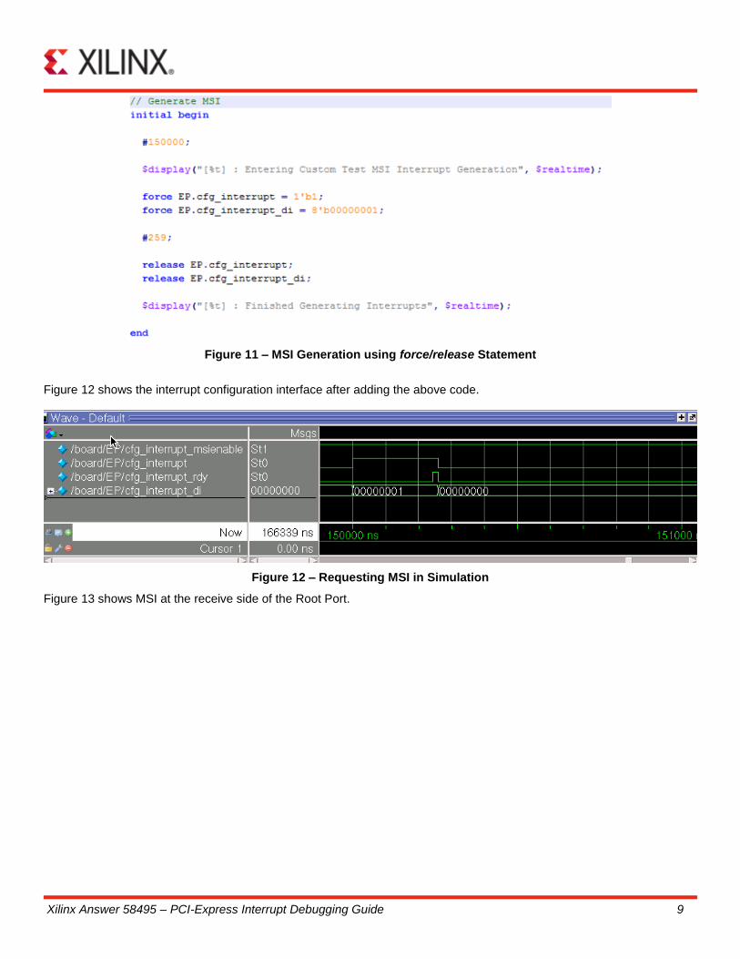
Xilinx Answer 58495 – PCI-Express Interrupt Debugging Guide 9
Figure 11 – MSI Generation using force/release Statement
Figure 12 shows the interrupt configuration interface after adding the above code.
Figure 12 – Requesting MSI in Simulation
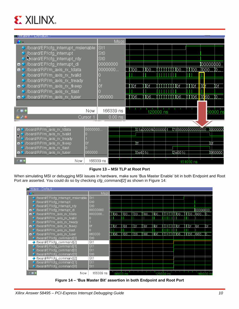
Figure 13 shows MSI at the receive side of the Root Port.
Xilinx Answer 58495 – PCI-Express Interrupt Debugging Guide 10
Figure 13 – MSI TLP at Root Port
When simulating MSI or debugging MSI issues in hardware, make sure ‘Bus Master Enable’ bit in both Endpoint and Root Port are asserted. You could do so by checking cfg_command[2] as shown in Figure 14:
Figure 14 – ‘Bus Master Bit’ assertion in both Endpoint and Root Port
Xilinx Answer 58495 – PCI-Express Interrupt Debugging Guide 11
Legacy Interrupt Simulation in PCIe Gen3 core
This section describes how to simulate legacy interrupt with PCIe Gen3 core example design. Below is a list of things that need to be done to successfully simulate legacy interrupt.
1. Make sure ‘Interrupt Disable’ bit in Command Register is not set in the endpoint.
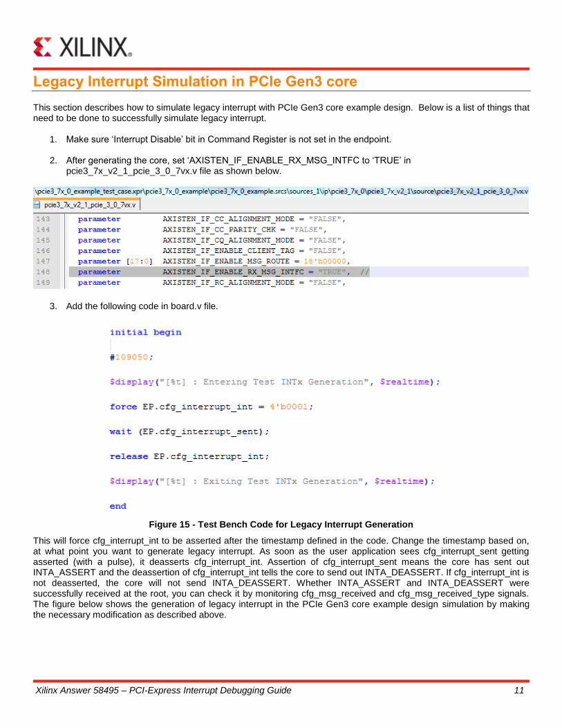
2. After generating the core, set ‘AXISTEN_IF_ENABLE_RX_MSG_INTFC to ‘TRUE’ in pcie3_7x_v2_1_pcie_3_0_7vx.v file as shown below.
3. Add the following code in board.v file.
Figure 15 - Test Bench Code for Legacy Interrupt Generation
This will force cfg_interrupt_int to be asserted after the timestamp defined in the code. Change the timestamp based on, at what point you want to generate legacy interrupt. As soon as the user application sees cfg_interrupt_sent getting asserted (with a pulse), it deasserts cfg_interrupt_int. Assertion of cfg_interrupt_sent means the core has sent out INTA_ASSERT and the deassertion of cfg_interrupt_int tells the core to send out INTA_DEASSERT. If cfg_interrupt_int is not deasserted, the core will not send INTA_DEASSERT. Whether INTA_ASSERT and INTA_DEASSERT were successfully received at the root, you can check it by monitoring cfg_msg_received and cfg_msg_received_type signals. The figure below shows the generation of legacy interrupt in the PCIe Gen3 core example design simulation by making the necessary modification as described above.
Xilinx Answer 58495 – PCI-Express Interrupt Debugging Guide 12
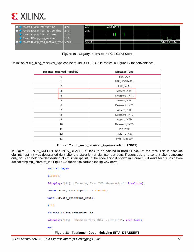
Figure 16 - Legacy Interrupt in PCIe Gen3 Core
Definition of cfg_msg_received_type can be found in PG023. It is shown in Figure 17 for convenience.
Figure 17 - cfg_msg_received_type encoding (PG023)
In Figure 16, INTA_ASSERT and INTA_DEASSERT look to be coming in back to back at the root. This is because cfg_interrupt_int was deasserted right after the assertion of cfg_interrupt_sent. If users desire to send it after sometime only, you can hold the deassertion of cfg_interrupt_int. In the code snippet shown in Figure 18, it waits for 100 ns before deasserting cfg_interrupt_int. Figure 19 shows the corresponding waveform.
Figure 18 - Testbench Code - delaying INTA_DEASSERT
Xilinx Answer 58495 – PCI-Express Interrupt Debugging Guide 13
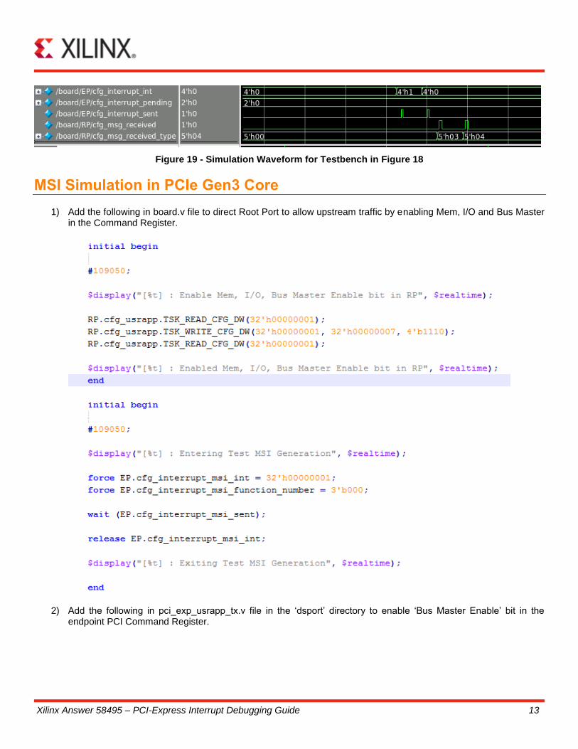
Figure 19 - Simulation Waveform for Testbench in Figure 18
MSI Simulation in PCIe Gen3 Core
1) Add the following in board.v file to direct Root Port to allow upstream traffic by enabling Mem, I/O and Bus Master in the Command Register.
2) Add the following in pci_exp_usrapp_tx.v file in the ‘dsport’ directory to enable ‘Bus Master Enable’ bit in the
endpoint PCI Command Register.
Xilinx Answer 58495 – PCI-Express Interrupt Debugging Guide 14
In the example design simulation, the configuration write task writes ‘4’ to the endpoint PCI command register. Change this to ‘7’ as shown above.
3) Program MSI Control Register to enable MSI. Add the following in pci_exp_usrapp_tx.v, in TSK_BAR_PROGRAM, in the ‘dsport’ directory.
Figure 20- MSI Control Register
4) Program Message Data Register. Add the following in pci_exp_usrapp_tx.v, in TSK_BAR_PROGRAM, in the
‘dsport’ directory.
Xilinx Answer 58495 – PCI-Express Interrupt Debugging Guide 15
MSI Control Register and Message Data Register Addressses
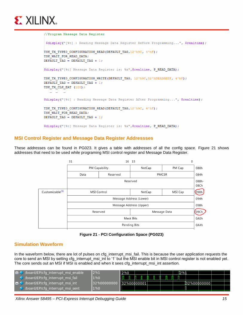
These addresses can be found in PG023. It gives a table with addresses of all the config space. Figure 21 shows addresses that need to be used while programing MSI control register and Message Data Register.
Figure 21 - PCI Configuration Space (PG023)
Simulation Waveform
In the waveform below, there are lot of pulses on cfg_interrupt_msi_fail. This is because the user application requests the core to send an MSI by setting cfg_interrupt_msi_int to ‘1’ but the MSI enable bit in MSI control register is not enabled yet. The core sends out an MSI if MSI is enabled and when it sees cfg_interrupt_msi_int assertion.

Xilinx Answer 58495 – PCI-Express Interrupt Debugging Guide 16
The MSI packet appears at the root port Completer Completion Interface as shown in Figure 22.
Figure 22 - MSI Packet at Root Port
Interrupts in Xilinx PCIe based Targeted Reference Designs
Xilinx Targeted Reference designs [4] support both MSI and Legacy interrupt. The details on this can be found in the respective user guides of the reference designs. In this section, a brief overview of what is required to be done at the driver level to enable MSI and Legacy interrupts is presented. The content and snapshots are from the drivers provided with the reference designs. For more details, please download the reference design and go through the provided source files. In the drivers provided with the reference design, interrupts are enabled by setting the compile-time macro TH_BH_ISR. The interrupt service routine (ISR) handles interrupts from the DMA engine. The driver sets up the DMA engine to interrupt after every N descriptor that it processes. This value of N can be set with a compile-time macro. The entire source code for the driver is provided with the reference design. Below are some of the key points that should be checked upfront while debugging MSI interrupt issues. 1) Check the device is MSI capable as shown in Figure 23.
Figure 23 - MSI Capability Check
2) MSI should be enabled with the pci_enable_msi( ) function call.

Xilinx Answer 58495 – PCI-Express Interrupt Debugging Guide 17
Figure 24 - Enabling interrupts in Targeted Reference Designs
3) The endpoint device must be set as Master to enable bus-mastering. This is done with pci_set_master( ) function call as shown in Figure 25.
Figure 25 - Enable Bus Master
4). In order to enable MSI in kernel, kernel should be built with CONFIG_PCI_MSI macro set to 1.
Things to Remember
The use of MSI or Legacy interrupt depends on whether MSI control register has MSI enable bit set or not. If it is set, MSI is used. If not Legacy interrupt is used. This bit is set by a configuration write from the root complex. Users cannot set this from the user application side of the core. So to set or unset this bit, user's device driver normally causes a configuration write to occur to the appropriate address (setting this bit to a 1 or 0).
It has been noticed that when the FPGA is using legacy interrupt, the interrupt lines are sometimes shared with other PCI Express devices. When the other PCI express devices send multiple interrupts to the host, the host must service all the interrupts that are associated with that interrupt line number which means that it might affect the performance of FPGA.
The MSI interrupt takes the form of a memory write request issued from the endpoint to the host. The endpoint needs to have its Bus Master enable bit set in order to send the Memory Write request transaction. Ensure that the Bus Master Enable bit is already set to 1 in the Command register in the PCI configuration space. This register should be set by the host at device initialization.
In 7 Series Integrated Block for PCI Express, make sure ENABLE_MSG_ROUTE is set to the following value: parameter [10:0] ENABLE_MSG_ROUTE = 11'b00000001000
While working with Legacy interrupts, make sure ‘Interrupt Disable’ bit in the command register is set to ‘0’.
Figure 26 - Interrupt Disable bit in Command Register
Xilinx Answer 58495 – PCI-Express Interrupt Debugging Guide 18
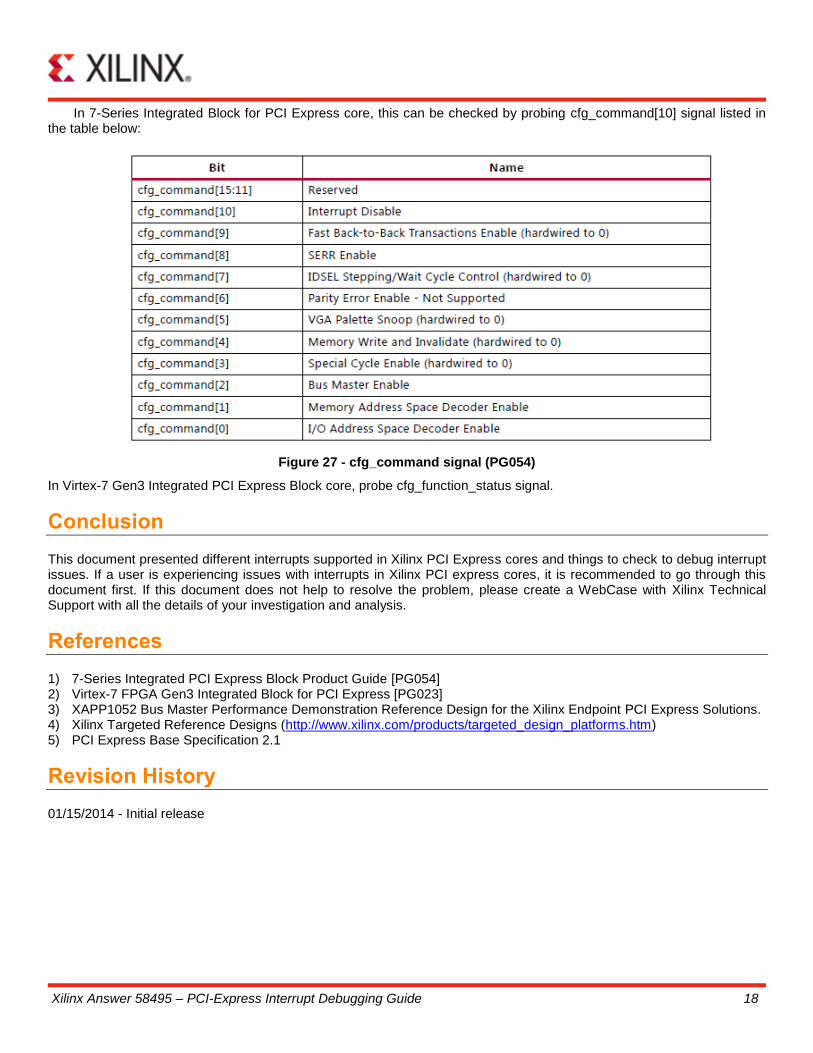
In 7-Series Integrated Block for PCI Express core, this can be checked by probing cfg_command[10] signal listed in the table below:
Figure 27 - cfg_command signal (PG054)
In Virtex-7 Gen3 Integrated PCI Express Block core, probe cfg_function_status signal.
Conclusion
This document presented different interrupts supported in Xilinx PCI Express cores and things to check to debug interrupt issues. If a user is experiencing issues with interrupts in Xilinx PCI express cores, it is recommended to go through this document first. If this document does not help to resolve the problem, please create a WebCase with Xilinx Technical Support with all the details of your investigation and analysis.
References
1) 7-Series Integrated PCI Express Block Product Guide [PG054] 2) Virtex-7 FPGA Gen3 Integrated Block for PCI Express [PG023] 3) XAPP1052 Bus Master Performance Demonstration Reference Design for the Xilinx Endpoint PCI Express Solutions. 4) Xilinx Targeted Reference Designs (http://www.xilinx.com/products/targeted_design_platforms.htm) 5) PCI Express Base Specification 2.1
Revision History
01/15/2014 - Initial release