Embed Size (px)
Citation preview

Xiaodong Wang (王晓冬 )
School of Nuclear Science and Technology Lanzhou University, Lanzhou, China
MPGD activities at Lanzhou University
July 5, 2013

Outline
Development of FEC for GASSIPLEX 0.7-3 chip
BulkMicromegas R&D base on T2K electronics
The status of GEM detector base on APV 25 chip
Simulations

GASSIPLEX 0.7-3 chip introduction
Gassiplex chip is used the 0.7 micron of CMOS technology. Peak forming time : 1.2usThe linear dynamic range is up to 560fC. Four components: charge sensitive amplifier, de-convolution filter, the shaper, track and hold circuit, 12 channels.

Peripheral analog circuit schematic of Gassipilex chip

Main control signals come from FPGA
Version-1
Test result
Development of FEC for GASSIPLEX 0.7-3 chip

Version-2
We got the basic conditions of the chip working status, such as the requirement of control signal, each pin circuit etc….
To reduce the volume and power consumption , all of the elements will be replace by piece components in next version.

PMT: CR115 of hamamatsu. Spectral response range :300-600 nm. peak value: 420nm, rise time : 2.2 ns
Trigger system :plastic scintillation detector
Schematic diagramResistor divider circuit
Emitter follower

Source :cosmic rays Voltage, 750 VLoad, 61 ohmAmplitude, 1VFall Time ,30 ns。
Assembly and test

• PCB: 365.5mm × 306.0mm• Sensitive area: 88.6mm
×57.4mm • Readout layout: 1728 pads • Each of 1.75mm × 1.50mm
http://mpgd.lzu.edu.cn/research.html
Fast neutron imaging exploiting BulkMicromegas base T2K electronics
n-HV1
-HV2
0
15mm
0.128mm
Ar+5% Isobutane
p
Micromesh
Pads Substrate
Aluminum polyethyleneDrift electrode
88.6mm
306.0mm
57.4mm
365.5mm

Experiment setup and target masks

Energy resolution calibration is irradiated with Fe-55.
Energy resolution ~25%( FWHM)Vmesh : 350V, Vdrift: 530V, Gain:5000
Detector energy resolution

The criterion of real signal and true track selection

Images of the test mask of LZU and CEA
Time cut
Images of boron-loaded polyethylene masks: LZU and CEA with Am-Be neutrons.
Time cut

Conversion efficiency and spatial resolution
According to the Edge Spread Function, we got the spatial
resolution, 1.55mm in X direction and 0.71 mm in Y direction.
Experiment detection efficiency :0.07% is lower than the simulation
result 0.08% .
Method I: Sharp Edge
Am-Be Neutron beam
CH2
Readout pads
Knife edge absorber

Spatial resolution II
Spatial resolution 2.04mm
Am-Be neutron beamMethod II: Collimator

New ideas:
1. Novel neutron-to-proton converter structures, base on Micromegas.
2. A new concept of neutron detector based on GEM technology is a novel multi-layer High Density PolyEthylene (HDPE) as neutron-to-proton converter.
Simulations

Parallel micro-pillar 2D arrayMicro-channel plate
Oblique micro-pillar 2D array
PE
film
Micro-hole
Parallel-pillar
45o inclined parallel-pillar
Am-Be
Neutrons
0.12%
0.152%+0.119%
0.271%
0.147%+0.096%
0.243%
0.310%+0.114%
0.424%
14MeV
Neutrons
0.35%
0.445%+0.376%
0.621%
0.403%+0.279%
0.662%
0.685%+0.330%
1.015%
SCI CHINA: Tech. Sci. 2013, 43( 3) 315-319
Monte Carlo simulation of BulkMicromegas-based for fast neutron detector

WANG Xiaodong, et al, SCIENCE CHINA Physics, Mechanics & Astronomy (2013) doi: 10.1007/s11433-013-5162-x
Detection efficiency of the detector with 400 converter units is higher than 2.3%.
Reconstruction accuracy of the incident neutron position is better than 2.6%.
Monte Carlo simulation of GEM-based for 14 MeV neutron detector
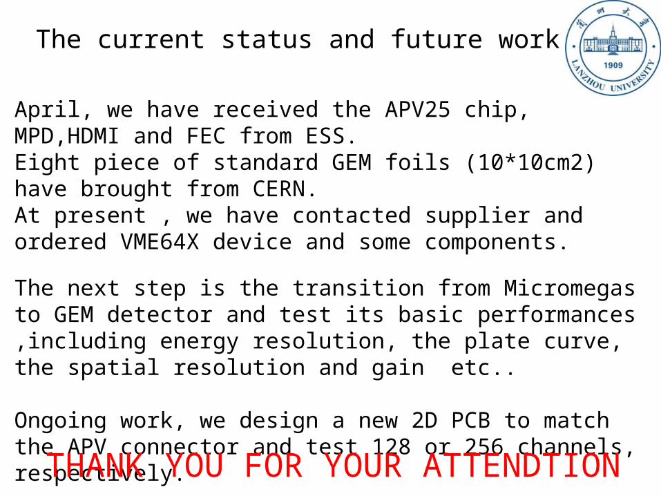
April, we have received the APV25 chip, MPD,HDMI and FEC from ESS.Eight piece of standard GEM foils (10*10cm2) have brought from CERN. At present , we have contacted supplier and ordered VME64X device and some components.
The next step is the transition from Micromegas to GEM detector and test its basic performances ,including energy resolution, the plate curve, the spatial resolution and gain etc..
Ongoing work, we design a new 2D PCB to match the APV connector and test 128 or 256 channels, respectively.
The current status and future work
THANK YOU FOR YOUR ATTENDTION