Embed Size (px)
Citation preview
WL1835MODCOM8B WLAN MIMO andBluetooth® Module Evaluation Board for TISitara™ Platform
User's Guide
Literature Number: SWRU359CSeptember 2013–Revised January 2014

Contents
Preface ....................................................................................................................................... 31 Introduction ........................................................................................................................ 4
1.1 Features .................................................................................................................. 51.2 Applications .............................................................................................................. 61.3 TI Module Key Benefits ................................................................................................. 61.4 Pin Descriptions ......................................................................................................... 81.5 VSWR ................................................................................................................... 101.6 Efficiency ................................................................................................................ 111.7 Radio Pattern ........................................................................................................... 111.8 Schematic ............................................................................................................... 151.9 Bill of Materials (BOM) ................................................................................................ 171.10 Board Layout ........................................................................................................... 18
2 Table of Contents SWRU359C–September 2013–Revised January 2014Submit Documentation Feedback
Copyright © 2013–2014, Texas Instruments Incorporated

PrefaceSWRU359C–September 2013–Revised January 2014
Read This First
About This ManualThis user's guide describes how to use the TI WL1835MODCOM8B board to evaluate the performance ofthe TI WL18MODGB module.
Related Documentation From Texas Instruments• TI WiLink8 Single-Band Combo Module – Wi-Fi, Bluetooth, and BLE (SWRS152)• WiLink 8 Wiki: http://www.ti.com/wilink8wiki
If You Need AssistanceThe primary sources of WL18MODGB information are the device-specific data sheets and user’s guides.For the most up-to-date version of the user’s guide and data sheets, go tohttp://www.ti.com/product/wl1835mod.
WarningThe WL1835MODCOM8B board is tested to comply with ETSI/R&TTE over temperatures from –20 to+70°C.
This board should not be modified to operate in other frequency bands other than what they are designedfor.
FCC Licensing Requirements for the Wi-Fi and Bluetooth Radio Module of the EVM:For evaluation only; not FCC approved for resale. This kit is designed to allow:1. Product developers to evaluate electronic components, circuitry, or software associated with the kit to
determine whether to incorporate such items in a finished product2. Software developers to write software applications for use with the end product. This kit is not a
finished product and when assembled may not be resold or otherwise marketed unless all requiredFCC equipment authorizations are first obtained. Operation is subject to the condition that this productnot cause harmful interference to licensed radio stations and that this product accept harmfulinterference. Unless the assembled kit is designed to operate under part 15, part 18, or part 95 of thischapter, the operator of the kit must operate under the authority of an FCC license holder or mustsecure an experimental authorization under part 5 of this chapter.
Per TI’s Regulatory Compliance Information located in the WL1835ModCOMB8B User’s Guide’s“Evaluation Board/Kit/Module (EVM) Additional Terms,” this EVM cannot be used for production purposesand is explicitly restricted from end-product introduction.
Use of this EVM requires the developer to provide a minimum distance of at least 20 cm from the antennato all persons in order to minimize risk of potential radiation hazards.
CAUTIONDo not leave the EVM powered when unattended.
3SWRU359C–September 2013–Revised January 2014 PrefaceSubmit Documentation Feedback
Copyright © 2013–2014, Texas Instruments Incorporated
FCC/IC Regulatory ComplianceFCC Part 15 Class A CompliantIC ICES-003 Class A Compliant
User's GuideSWRU359C–September 2013–Revised January 2014
WL1835MODCOM8B WLAN MIMO and Bluetooth® ModuleEvaluation Board for TI Sitara™ Platform
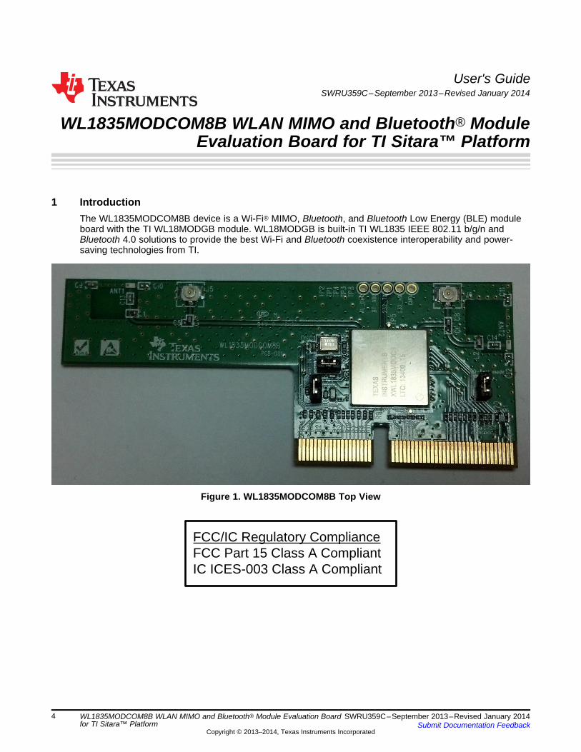
1 IntroductionThe WL1835MODCOM8B device is a Wi-Fi® MIMO, Bluetooth, and Bluetooth Low Energy (BLE) moduleboard with the TI WL18MODGB module. WL18MODGB is built-in TI WL1835 IEEE 802.11 b/g/n andBluetooth 4.0 solutions to provide the best Wi-Fi and Bluetooth coexistence interoperability and power-saving technologies from TI.
Figure 1. WL1835MODCOM8B Top View
4 WL1835MODCOM8B WLAN MIMO and Bluetooth® Module Evaluation Board SWRU359C–September 2013–Revised January 2014for TI Sitara™ Platform Submit Documentation Feedback
Copyright © 2013–2014, Texas Instruments Incorporated
IC ID: 451I-WL1835COM
This device complies with Industry Canada licence-exempt RSS standard(s). Operation is subject to the following two conditions: (1) this device may not cause interference, and (2) this device must accept any interference, including that may cause undesired operation of the device.
FCC ID: Z64-WL1835COM
This device complies with part 15 of the FCC Rules. Operation is subject to the following two conditions: (1) This device may not cause harmful interference, and (2) this device must accept any interference received, including interference that may cause undesired operation.
www.ti.com Introduction
(continued)
1.1 Features• WLAN, Bluetooth, BLE on a module board• 100-pin board card• Dimension 76.0 mm(L) x 31.0 mm(W)• WLAN 2.4 GHz SISO (20- and 40-MHz channels), 2.4-GHz MIMO (20-MHz channels)• Support for BLE dual mode• Seamless integration with TI Sitara and other application processors• Design for TI AM335X general-purpose EVM• WLAN and Bluetooth, BLE cores are software and hardware compatible with prior WL127x, WL128x
and CC256x offerings, for smooth migration to device.• Shared HCI transport for Bluetooth and BLE over UART and SDIO for WLAN.• Wi-Fi / Bluetooth single antenna co-existence• Built-in chip antenna• Optional U.FL RF connector for external 2.4-GHz band antenna• Direct connection to battery using external switching mode power supply supporting 4.8-V to 2.9-V
operation• VIO in the 1.8-V domain
5SWRU359C–September 2013–Revised January 2014 WL1835MODCOM8B WLAN MIMO and Bluetooth® Module Evaluation Boardfor TI Sitara™ PlatformSubmit Documentation Feedback
Copyright © 2013–2014, Texas Instruments Incorporated
Introduction www.ti.com
1.2 Applications• Internet of Things Multimedia• Home Electronics• Home Appliances and White Goods• Industrial and Home Automation• Smart Gateway and Metering• Video Conferencing• Video Camera and Security
1.3 TI Module Key Benefits• Reduces Design Overhead: Single WiLink8™ Module Scales Across Wi-Fi and Bluetooth.• WLAN High Throughput: 80 Mbps (TCP), 100 Mbps (UDP)• Bluetooth 4.0 + BLE (Smart Ready)• Wi-Fi-Bluetooth Single Antenna Coexistence• Low Power (30–50% Less than Previous Generation)• Available as Easy-to-Use FCC, ETSI, and Telec Certified Module• Lower Manufacturing Costs, Saving Board Space and Minimizing RF Expertise• AM335x Linux® and Android™ Reference Platform Accelerates Customer Development and Time to
Market
6 WL1835MODCOM8B WLAN MIMO and Bluetooth® Module Evaluation Board SWRU359C–September 2013–Revised January 2014for TI Sitara™ Platform Submit Documentation Feedback
Copyright © 2013–2014, Texas Instruments Incorporated

U1
WL18MODGB
www.ti.com Introduction
Board Pin Assignment
Figure 2. Board Top View
Figure 3. Board Bottom View
7SWRU359C–September 2013–Revised January 2014 WL1835MODCOM8B WLAN MIMO and Bluetooth® Module Evaluation Boardfor TI Sitara™ PlatformSubmit Documentation Feedback
Copyright © 2013–2014, Texas Instruments Incorporated
Introduction www.ti.com
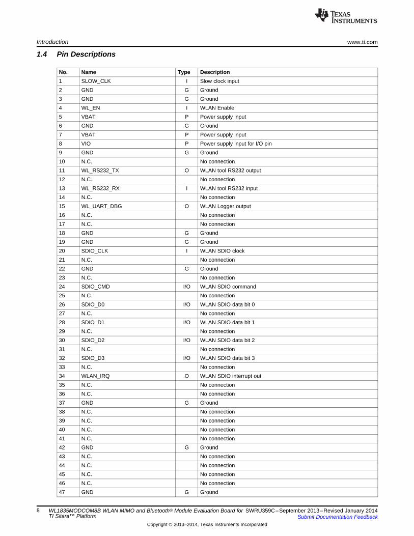
1.4 Pin Descriptions
No. Name Type Description1 SLOW_CLK I Slow clock input2 GND G Ground3 GND G Ground4 WL_EN I WLAN Enable5 VBAT P Power supply input6 GND G Ground7 VBAT P Power supply input8 VIO P Power supply input for I/O pin9 GND G Ground10 N.C. No connection11 WL_RS232_TX O WLAN tool RS232 output12 N.C. No connection13 WL_RS232_RX I WLAN tool RS232 input14 N.C. No connection15 WL_UART_DBG O WLAN Logger output16 N.C. No connection17 N.C. No connection18 GND G Ground19 GND G Ground20 SDIO_CLK I WLAN SDIO clock21 N.C. No connection22 GND G Ground23 N.C. No connection24 SDIO_CMD I/O WLAN SDIO command25 N.C. No connection26 SDIO_D0 I/O WLAN SDIO data bit 027 N.C. No connection28 SDIO_D1 I/O WLAN SDIO data bit 129 N.C. No connection30 SDIO_D2 I/O WLAN SDIO data bit 231 N.C. No connection32 SDIO_D3 I/O WLAN SDIO data bit 333 N.C. No connection34 WLAN_IRQ O WLAN SDIO interrupt out35 N.C. No connection36 N.C. No connection37 GND G Ground38 N.C. No connection39 N.C. No connection40 N.C. No connection41 N.C. No connection42 GND G Ground43 N.C. No connection44 N.C. No connection45 N.C. No connection46 N.C. No connection47 GND G Ground
8 WL1835MODCOM8B WLAN MIMO and Bluetooth® Module Evaluation Board for SWRU359C–September 2013–Revised January 2014TI Sitara™ Platform Submit Documentation Feedback
Copyright © 2013–2014, Texas Instruments Incorporated
www.ti.com Introduction
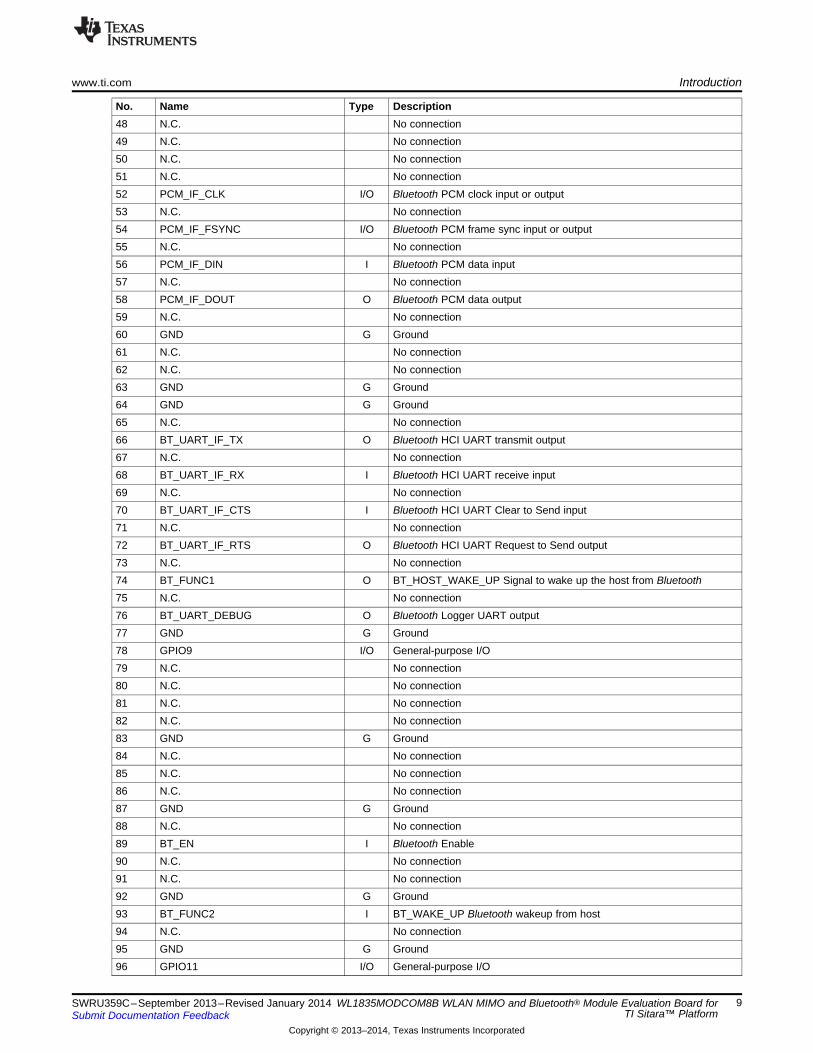
No. Name Type Description48 N.C. No connection49 N.C. No connection50 N.C. No connection51 N.C. No connection52 PCM_IF_CLK I/O Bluetooth PCM clock input or output53 N.C. No connection54 PCM_IF_FSYNC I/O Bluetooth PCM frame sync input or output55 N.C. No connection56 PCM_IF_DIN I Bluetooth PCM data input57 N.C. No connection58 PCM_IF_DOUT O Bluetooth PCM data output59 N.C. No connection60 GND G Ground61 N.C. No connection62 N.C. No connection63 GND G Ground64 GND G Ground65 N.C. No connection66 BT_UART_IF_TX O Bluetooth HCI UART transmit output67 N.C. No connection68 BT_UART_IF_RX I Bluetooth HCI UART receive input69 N.C. No connection70 BT_UART_IF_CTS I Bluetooth HCI UART Clear to Send input71 N.C. No connection72 BT_UART_IF_RTS O Bluetooth HCI UART Request to Send output73 N.C. No connection74 BT_FUNC1 O BT_HOST_WAKE_UP Signal to wake up the host from Bluetooth75 N.C. No connection76 BT_UART_DEBUG O Bluetooth Logger UART output77 GND G Ground78 GPIO9 I/O General-purpose I/O79 N.C. No connection80 N.C. No connection81 N.C. No connection82 N.C. No connection83 GND G Ground84 N.C. No connection85 N.C. No connection86 N.C. No connection87 GND G Ground88 N.C. No connection89 BT_EN I Bluetooth Enable90 N.C. No connection91 N.C. No connection92 GND G Ground93 BT_FUNC2 I BT_WAKE_UP Bluetooth wakeup from host94 N.C. No connection95 GND G Ground96 GPIO11 I/O General-purpose I/O
9SWRU359C–September 2013–Revised January 2014 WL1835MODCOM8B WLAN MIMO and Bluetooth® Module Evaluation Board forTI Sitara™ PlatformSubmit Documentation Feedback
Copyright © 2013–2014, Texas Instruments Incorporated

Introduction www.ti.com
No. Name Type Description97 GND G Ground98 GPIO12 I/O General-purpose I/O99 N.C. General-purpose I/O100 GPIO10 I/O General-purpose I/O
Electrical CharacteristicsRefer to the detailed data in the WL18MODGB data sheet for electrical characteristics.
Antenna Characteristics
1.5 VSWRFigure 4 shows the antenna VSWR.
Figure 4. Antenna VSWR
10 WL1835MODCOM8B WLAN MIMO and Bluetooth® Module Evaluation Board SWRU359C–September 2013–Revised January 2014for TI Sitara™ Platform Submit Documentation Feedback
Copyright © 2013–2014, Texas Instruments Incorporated
www.ti.com Introduction
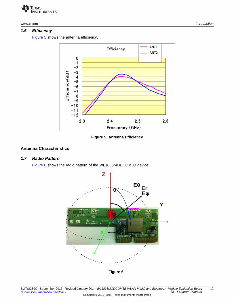
1.6 EfficiencyFigure 5 shows the antenna efficiency.
Figure 5. Antenna Efficiency
Antenna Characteristics
1.7 Radio PatternFigure 6 shows the radio pattern of the WL1835MODCOM8B device.
Figure 6.
11SWRU359C–September 2013–Revised January 2014 WL1835MODCOM8B WLAN MIMO and Bluetooth® Module Evaluation Boardfor TI Sitara™ PlatformSubmit Documentation Feedback
Copyright © 2013–2014, Texas Instruments Incorporated
Introduction www.ti.com
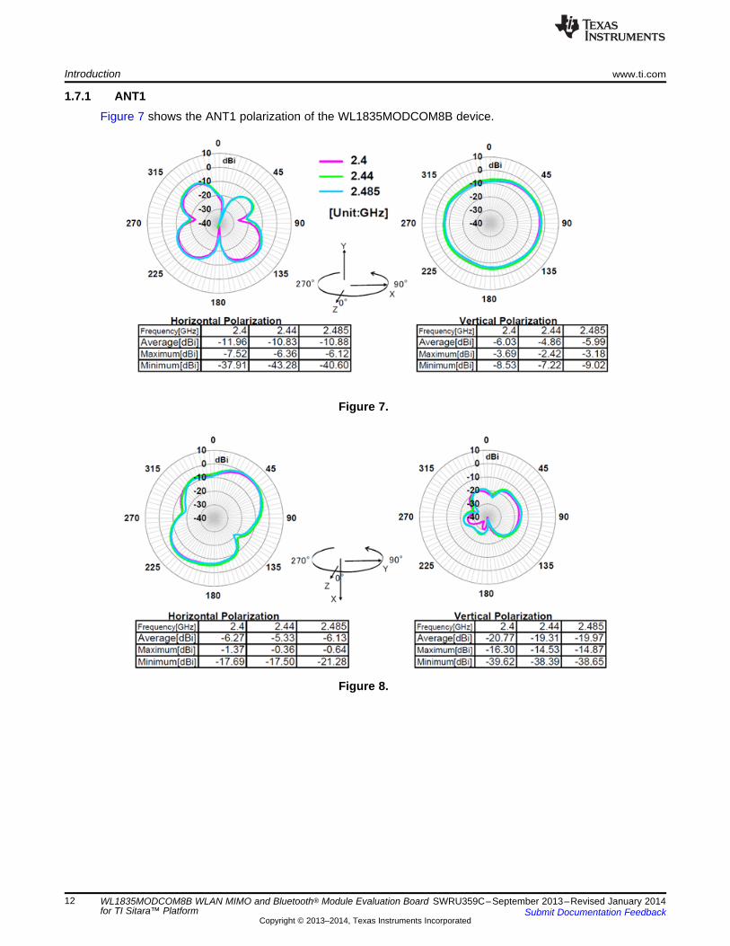
1.7.1 ANT1Figure 7 shows the ANT1 polarization of the WL1835MODCOM8B device.
Figure 7.
Figure 8.
12 WL1835MODCOM8B WLAN MIMO and Bluetooth® Module Evaluation Board SWRU359C–September 2013–Revised January 2014for TI Sitara™ Platform Submit Documentation Feedback
Copyright © 2013–2014, Texas Instruments Incorporated
www.ti.com Introduction
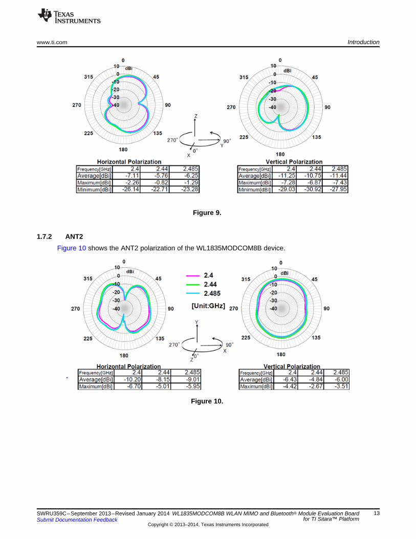
Figure 9.
1.7.2 ANT2Figure 10 shows the ANT2 polarization of the WL1835MODCOM8B device.
Figure 10.
13SWRU359C–September 2013–Revised January 2014 WL1835MODCOM8B WLAN MIMO and Bluetooth® Module Evaluation Boardfor TI Sitara™ PlatformSubmit Documentation Feedback
Copyright © 2013–2014, Texas Instruments Incorporated

Introduction www.ti.com
Figure 11.
Figure 12.
14 WL1835MODCOM8B WLAN MIMO and Bluetooth® Module Evaluation Board SWRU359C–September 2013–Revised January 2014for TI Sitara™ Platform Submit Documentation Feedback
Copyright © 2013–2014, Texas Instruments Incorporated
EDGE CONNECTOR - MALE
WL_BG ANT2WL_BG/BT ANT1
Short PIN Header (1-2)for entering test mode.Open for function mode.
These two TPs for test modewhen WL_IRQ pull high.
WL_UART_DBG
BT_AUD_CLK
BT_AUD_FSYNC
BT_AUD_IN
WL_RS232_TX
WL_RS232_RX
BT_HCI_TX
BT_HCI_RX
BT_HCI_CTS
BT_HCI_RTS
BT_EN_SOC
BT_UART_DBG
SDIO_CLK_WL
SDIO_CMD_WL
SDIO_D0_WL
SDIO_D2_WL
SDIO_D3_WL
SDIO_D1_WL
WLAN_EN_SOC
BT_AUD_OUT
BT_FUNC1
GPIO9
GPIO11
GPIO12
GPIO10
SLOW_CLK
BT_FUNC2
WLAN_IRQ
2G4_ANT1_WB2G4_ANT2_W
SDIO_D3_WL
GPIO12
SDIO_D2_WL
GPIO11
SDIO_D0_WL
SDIO_D1_WL
GPIO9
WLAN_IRQ
GPIO10
2G4_ANT2_W
WL_RS232_TX
WL_RS232_RX
2G4_ANT1_WB
BT_FUNC1
BT_FUNC2
BT_HCI_RX
BT_HCI_TX
BT_HCI_CTS
BT_HCI_RTS
BT_AUD_IN
BT_AUD_OUT
BT_AUD_CLK
BT_AUD_FSYNC
SDIO_CMD_WL
SDIO_CLK_WL
SLOW_CLK
WL_UART_DBG
BT_UART_DBG
BT_EN_SOC
WLAN_EN_SOC
VBAT_IN
VIO_IN
VIO_IN
VBAT_IN
VIO_IN
VIO_IN
R20 10k0402
R25 0R 0402
C510pF0402
J6U.FL-R-SMT(10)U.FL
12
3
C144pF0402
ANT2ANT016008LCD2442MA1ANT-N3-1.6X0.8MM-B
5G
B2
FEEDA
2.4G
B1
R17 0R 0402
C610pF0402
J2NU_100pin Micro Edge MEC6SD-100P
1 2
3 4
5 6
7 8
9 10
11 12
13 14
15 16
17 18
19 20
21 22
23 24
25 26
27 28
29 30
31 32
33 34
35 36
37 38
39 40
41 42
43 44
45 46
47 48
49 50
51 52
53 54
55 56
57 58
59 60
61 62
63 64
65 66
67 68
69 70
71 72
73 74
75 76
77 78
79 80
81 82
83 84
85 86
87 88
89 90
91 92
93 94
95 96
97 98
99 100
TP41
C7NU_10pF0402 C9
2pF0402
R12 0R 0402
C111.2pF0402
R11 0R 0402
ANT1ANT016008LCD2442MA1ANT-N3-1.6X0.8MM-A
5G
B2
FEEDA
2.4G
B1
C11uF0402
R30 0R 0402
R9 0R 0402
J5U.FL-R-SMT(10)U.FL
12
3
C10NU_0.3pF0402
R10 0R0402
TP1 1
TP51
R2 0R 0402
0RR21 0402
TP6 1
0RR19 0402
OSC11V8 / 32.768kHzOSC-3.2X2.5
EN1
VCC4
OUT3
GND2
R60R0402
R3 0R 0402
R16 0R 0402
U1
WL1835MODGB
E-13.4X13.3-N100_0.75-TOP
GP
IO9
3
GP
IO12
5
GP
IO11
2
GP
IO10
4
GND17
VIO
38
VB
AT
47
EX
T_
32
K3
6
BT_AUD_FSYNC58
BT_AUD_IN56
BT_AUD_OUT57
BT_AUD_CLK60
WL_S
DIO
_D
212
WL_S
DIO
_C
LK
8
WL_S
DIO
_D
313
WL_S
DIO
_D
010
WL_S
DIO
_D
111
WL_S
DIO
_C
MD
6
BT_HCI_RTS50
BT_HCI_RX53
BT_HCI_TX52
BT_HCI_CTS51
GN
D16
GPIO_425
GPIO_226
GPIO_127
BT
_E
N_S
OC
41
WLA
N_IR
Q14
WLA
N_E
N_S
OC
40
BT
_U
AR
T_D
BG
43
WL_U
AR
T_D
BG
42
GNDG13
GNDG14
GNDG15
GNDG16
GNDG9
GNDG10
GN
D48
GNDG11
GNDG12
VB
AT
46
GND28
GNDG1
GNDG2
GNDG3
GNDG4
GNDG5
GNDG6
GNDG7
GNDG8
2G4_ANT1_WB32
GND64
GN
D1
GND20
RESERVED121
RESERVED222
GN
D37
GND19
RESERVED362
GNDG17
GNDG18
GNDG19
GNDG20
GNDG21
GNDG22
GNDG23
GNDG24
GNDG25
GNDG26
GNDG27
GNDG28
GNDG29
GNDG30
GNDG31
GNDG32
GNDG33
GNDG34
GNDG35
GND23
GND59
GN
D34
GND29
GN
D7
2G4_ANT2_W18
GND49
GN
D9
GND31
GN
D35
GN
D15
GND55
GN
D45
GN
D44
GND30
GND24
GND63
GND61
GN
D39
GN
D33
GND54
GNDG36
C210uF0603
R310R0402
J1HEADER 1x2H-1X2_2MM
12
R1 0R 0402
R29 0R 0402
R8 0R 0402
L1
04021.1nH
TP31
R28 0R 0402
0RR24 0402
R7 0R 0402
TP8 1
R14 0R 0402
C8NU_10pF0402
C40.1uF0402
R27 0R 0402
R13 0R 0402
R15 0R 0402
C30.1uF0402
0RR22 0402
R18 0R 0402
R4 0R 0402
R23 0R 0402
R320R0402
C138pF0402
R5 NU_0R0402
C12NU0402
J3HEADER 1x2H-1X2_2MM
12
J4HEADER 1x2H-1X2_2MM
1 2
0RR26 0402
L21.5nH0402
TP2 1
www.ti.com Introduction
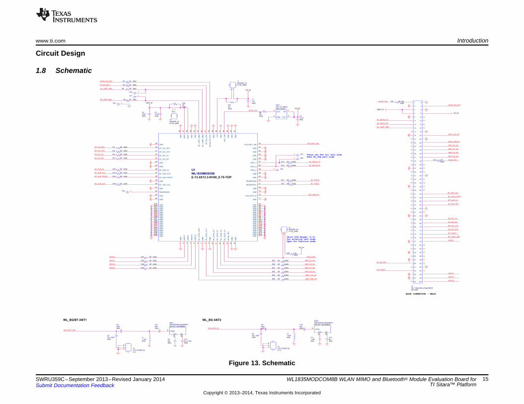
Circuit Design
1.8 Schematic
Figure 13. Schematic
15SWRU359C–September 2013–Revised January 2014 WL1835MODCOM8B WLAN MIMO and Bluetooth® Module Evaluation Board forTI Sitara™ PlatformSubmit Documentation Feedback
Copyright © 2013–2014, Texas Instruments Incorporated

Introduction www.ti.com
16 WL1835MODCOM8B WLAN MIMO and Bluetooth® Module Evaluation Board for SWRU359C–September 2013–Revised January 2014TI Sitara™ Platform Submit Documentation Feedback
Copyright © 2013–2014, Texas Instruments Incorporated
www.ti.com Introduction
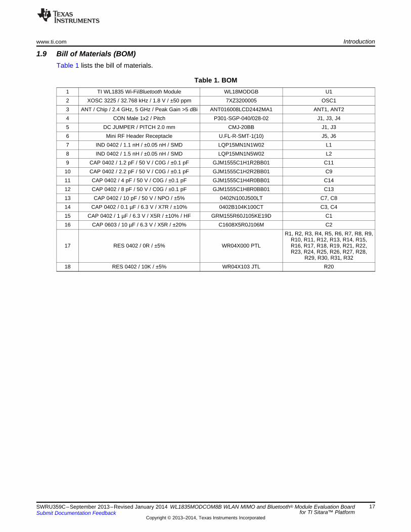
1.9 Bill of Materials (BOM)Table 1 lists the bill of materials.
Table 1. BOM1 TI WL1835 Wi-Fi/Bluetooth Module WL18MODGB U12 XOSC 3225 / 32.768 kHz / 1.8 V / ±50 ppm 7XZ3200005 OSC13 ANT / Chip / 2.4 GHz, 5 GHz / Peak Gain >5 dBi ANT016008LCD2442MA1 ANT1, ANT24 CON Male 1x2 / Pitch P301-SGP-040/028-02 J1, J3, J45 DC JUMPER / PITCH 2.0 mm CMJ-20BB J1, J36 Mini RF Header Receptacle U.FL-R-SMT-1(10) J5, J67 IND 0402 / 1.1 nH / ±0.05 nH / SMD LQP15MN1N1W02 L18 IND 0402 / 1.5 nH / ±0.05 nH / SMD LQP15MN1N5W02 L29 CAP 0402 / 1.2 pF / 50 V / C0G / ±0.1 pF GJM1555C1H1R2BB01 C1110 CAP 0402 / 2.2 pF / 50 V / C0G / ±0.1 pF GJM1555C1H2R2BB01 C911 CAP 0402 / 4 pF / 50 V / C0G / ±0.1 pF GJM1555C1H4R0BB01 C1412 CAP 0402 / 8 pF / 50 V / C0G / ±0.1 pF GJM1555C1H8R0BB01 C1313 CAP 0402 / 10 pF / 50 V / NPO / ±5% 0402N100J500LT C7, C814 CAP 0402 / 0.1 µF / 6.3 V / X7R / ±10% 0402B104K100CT C3, C415 CAP 0402 / 1 µF / 6.3 V / X5R / ±10% / HF GRM155R60J105KE19D C116 CAP 0603 / 10 µF / 6.3 V / X5R / ±20% C1608X5R0J106M C2
R1, R2, R3, R4, R5, R6, R7, R8, R9,R10, R11, R12, R13, R14, R15,
17 RES 0402 / 0R / ±5% WR04X000 PTL R16, R17, R18, R19, R21, R22,R23, R24, R25, R26, R27, R28,
R29, R30, R31, R3218 RES 0402 / 10K / ±5% WR04X103 JTL R20
17SWRU359C–September 2013–Revised January 2014 WL1835MODCOM8B WLAN MIMO and Bluetooth® Module Evaluation Boardfor TI Sitara™ PlatformSubmit Documentation Feedback
Copyright © 2013–2014, Texas Instruments Incorporated

Introduction www.ti.com
Layout Guidelines
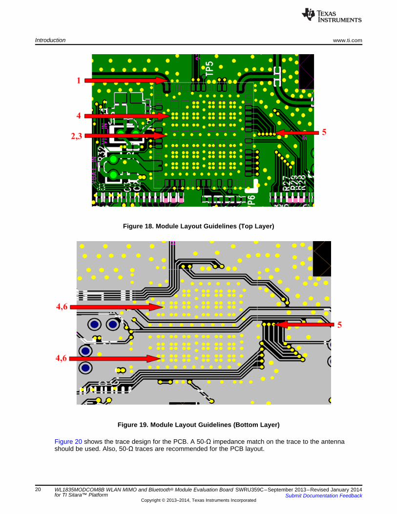
1.10 Board LayoutFigure 14 shows the WL1835MODCOM8B 4-layer board. Table 2, Figure 15, Figure 16, Figure 17,Figure 18, and Figure 19 show instances of good layout practices.
Figure 14. Layer 1
Figure 15. Layer 2
18 WL1835MODCOM8B WLAN MIMO and Bluetooth® Module Evaluation Board SWRU359C–September 2013–Revised January 2014for TI Sitara™ Platform Submit Documentation Feedback
Copyright © 2013–2014, Texas Instruments Incorporated
www.ti.com Introduction
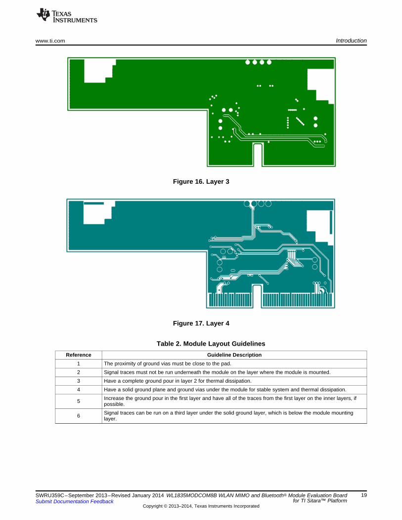
Figure 16. Layer 3
Figure 17. Layer 4
Table 2. Module Layout GuidelinesReference Guideline Description
1 The proximity of ground vias must be close to the pad.2 Signal traces must not be run underneath the module on the layer where the module is mounted.3 Have a complete ground pour in layer 2 for thermal dissipation.4 Have a solid ground plane and ground vias under the module for stable system and thermal dissipation.
Increase the ground pour in the first layer and have all of the traces from the first layer on the inner layers, if5 possible.Signal traces can be run on a third layer under the solid ground layer, which is below the module mounting6 layer.
19SWRU359C–September 2013–Revised January 2014 WL1835MODCOM8B WLAN MIMO and Bluetooth® Module Evaluation Boardfor TI Sitara™ PlatformSubmit Documentation Feedback
Copyright © 2013–2014, Texas Instruments Incorporated
Introduction www.ti.com
Figure 18. Module Layout Guidelines (Top Layer)
Figure 19. Module Layout Guidelines (Bottom Layer)
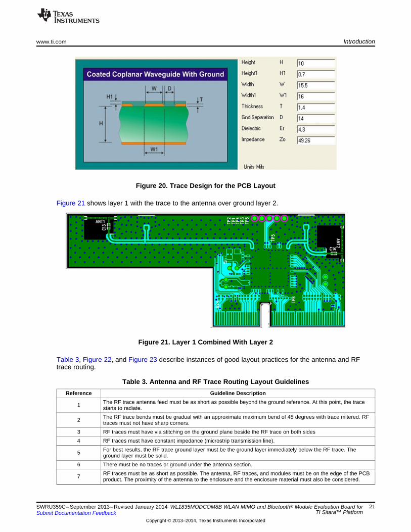
Figure 20 shows the trace design for the PCB. A 50-Ω impedance match on the trace to the antennashould be used. Also, 50-Ω traces are recommended for the PCB layout.
20 WL1835MODCOM8B WLAN MIMO and Bluetooth® Module Evaluation Board SWRU359C–September 2013–Revised January 2014for TI Sitara™ Platform Submit Documentation Feedback
Copyright © 2013–2014, Texas Instruments Incorporated
www.ti.com Introduction
Figure 20. Trace Design for the PCB Layout
Figure 21 shows layer 1 with the trace to the antenna over ground layer 2.
Figure 21. Layer 1 Combined With Layer 2
Table 3, Figure 22, and Figure 23 describe instances of good layout practices for the antenna and RFtrace routing.
Table 3. Antenna and RF Trace Routing Layout GuidelinesReference Guideline Description
The RF trace antenna feed must be as short as possible beyond the ground reference. At this point, the trace1 starts to radiate.The RF trace bends must be gradual with an approximate maximum bend of 45 degrees with trace mitered. RF2 traces must not have sharp corners.
3 RF traces must have via stitching on the ground plane beside the RF trace on both sides4 RF traces must have constant impedance (microstrip transmission line).
For best results, the RF trace ground layer must be the ground layer immediately below the RF trace. The5 ground layer must be solid.6 There must be no traces or ground under the antenna section.
RF traces must be as short as possible. The antenna, RF traces, and modules must be on the edge of the PCB7 product. The proximity of the antenna to the enclosure and the enclosure material must also be considered.
21SWRU359C–September 2013–Revised January 2014 WL1835MODCOM8B WLAN MIMO and Bluetooth® Module Evaluation Board forTI Sitara™ PlatformSubmit Documentation Feedback
Copyright © 2013–2014, Texas Instruments Incorporated

Introduction www.ti.com
Figure 22. Top Layer – Antenna and RF Trace Routing Layout Guidelines
Figure 23. Bottom Layer – Antenna and RF Trace Routing Layout Guidelines
22 WL1835MODCOM8B WLAN MIMO and Bluetooth® Module Evaluation Board SWRU359C–September 2013–Revised January 2014for TI Sitara™ Platform Submit Documentation Feedback
Copyright © 2013–2014, Texas Instruments Incorporated
www.ti.com Introduction
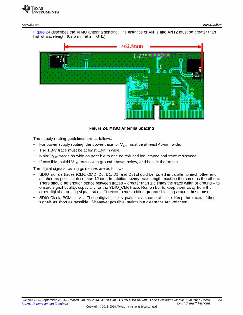
Figure 24 describes the MIMO antenna spacing. The distance of ANT1 and ANT2 must be greater thanhalf of wavelength (62.5 mm at 2.4 GHz).
Figure 24. MIMO Antenna Spacing
The supply routing guidelines are as follows:• For power supply routing, the power trace for VBAT must be at least 40-mm wide.• The 1.8-V trace must be at least 18-mm wide.• Make VBAT traces as wide as possible to ensure reduced inductance and trace resistance.• If possible, shield VBAT traces with ground above, below, and beside the traces.
The digital signals routing guidelines are as follows:• SDIO signals traces (CLK, CMD, D0, D1, D2, and D3) should be routed in parallel to each other and
as short as possible (less than 12 cm). In addition, every trace length must be the same as the others.There should be enough space between traces – greater than 1.5 times the trace width or ground – toensure signal quality, especially for the SDIO_CLK trace. Remember to keep them away from theother digital or analog signal traces. TI recommends adding ground shielding around these buses.
• SDIO Clock, PCM clock… These digital clock signals are a source of noise. Keep the traces of thesesignals as short as possible. Whenever possible, maintain a clearance around them.
23SWRU359C–September 2013–Revised January 2014 WL1835MODCOM8B WLAN MIMO and Bluetooth® Module Evaluation Boardfor TI Sitara™ PlatformSubmit Documentation Feedback
Copyright © 2013–2014, Texas Instruments Incorporated
Revision History www.ti.com
This user's guide revision history highlights the technical changes made to the SWRU359 device-specific user'sguide.
Revision HistoryRevision Date Description / Changes
Changed all references of the module fromWL1835MODGB to WL18MODGB.
SWRS359C January 2014In Warning: Changed tested-temperature range from 0 –+70, to –20 – +70.
NOTE: Page numbers for previous revisions may differ from page numbers in the current version.
24 Revision History SWRU359C–September 2013–Revised January 2014Submit Documentation Feedback
Copyright © 2013–2014, Texas Instruments Incorporated
STANDARD TERMS AND CONDITIONS FOR EVALUATION MODULES1. Delivery: TI delivers TI evaluation boards, kits, or modules, including any accompanying demonstration software, components, or
documentation (collectively, an “EVM” or “EVMs”) to the User (“User”) in accordance with the terms and conditions set forth herein.Acceptance of the EVM is expressly subject to the following terms and conditions.1.1 EVMs are intended solely for product or software developers for use in a research and development setting to facilitate feasibility
evaluation, experimentation, or scientific analysis of TI semiconductors products. EVMs have no direct function and are notfinished products. EVMs shall not be directly or indirectly assembled as a part or subassembly in any finished product. Forclarification, any software or software tools provided with the EVM (“Software”) shall not be subject to the terms and conditionsset forth herein but rather shall be subject to the applicable terms and conditions that accompany such Software
1.2 EVMs are not intended for consumer or household use. EVMs may not be sold, sublicensed, leased, rented, loaned, assigned,or otherwise distributed for commercial purposes by Users, in whole or in part, or used in any finished product or productionsystem.
2 Limited Warranty and Related Remedies/Disclaimers:2.1 These terms and conditions do not apply to Software. The warranty, if any, for Software is covered in the applicable Software
License Agreement.2.2 TI warrants that the TI EVM will conform to TI's published specifications for ninety (90) days after the date TI delivers such EVM
to User. Notwithstanding the foregoing, TI shall not be liable for any defects that are caused by neglect, misuse or mistreatmentby an entity other than TI, including improper installation or testing, or for any EVMs that have been altered or modified in anyway by an entity other than TI. Moreover, TI shall not be liable for any defects that result from User's design, specifications orinstructions for such EVMs. Testing and other quality control techniques are used to the extent TI deems necessary or asmandated by government requirements. TI does not test all parameters of each EVM.
2.3 If any EVM fails to conform to the warranty set forth above, TI's sole liability shall be at its option to repair or replace such EVM,or credit User's account for such EVM. TI's liability under this warranty shall be limited to EVMs that are returned during thewarranty period to the address designated by TI and that are determined by TI not to conform to such warranty. If TI elects torepair or replace such EVM, TI shall have a reasonable time to repair such EVM or provide replacements. Repaired EVMs shallbe warranted for the remainder of the original warranty period. Replaced EVMs shall be warranted for a new full ninety (90) daywarranty period.
3 Regulatory Notices:3.1 United States
3.1.1 Notice applicable to EVMs not FCC-Approved:This kit is designed to allow product developers to evaluate electronic components, circuitry, or software associated with the kitto determine whether to incorporate such items in a finished product and software developers to write software applications foruse with the end product. This kit is not a finished product and when assembled may not be resold or otherwise marketed unlessall required FCC equipment authorizations are first obtained. Operation is subject to the condition that this product not causeharmful interference to licensed radio stations and that this product accept harmful interference. Unless the assembled kit isdesigned to operate under part 15, part 18 or part 95 of this chapter, the operator of the kit must operate under the authority ofan FCC license holder or must secure an experimental authorization under part 5 of this chapter.3.1.2 For EVMs annotated as FCC – FEDERAL COMMUNICATIONS COMMISSION Part 15 Compliant:
CAUTIONThis device complies with part 15 of the FCC Rules. Operation is subject to the following two conditions: (1) This device may notcause harmful interference, and (2) this device must accept any interference received, including interference that may causeundesired operation.Changes or modifications not expressly approved by the party responsible for compliance could void the user's authority tooperate the equipment.
FCC Interference Statement for Class A EVM devicesNOTE: This equipment has been tested and found to comply with the limits for a Class A digital device, pursuant to part 15 ofthe FCC Rules. These limits are designed to provide reasonable protection against harmful interference when the equipment isoperated in a commercial environment. This equipment generates, uses, and can radiate radio frequency energy and, if notinstalled and used in accordance with the instruction manual, may cause harmful interference to radio communications.Operation of this equipment in a residential area is likely to cause harmful interference in which case the user will be required tocorrect the interference at his own expense.
SPACER
SPACER
SPACER
SPACER
SPACER
SPACER
SPACER
SPACER

FCC Interference Statement for Class B EVM devicesNOTE: This equipment has been tested and found to comply with the limits for a Class B digital device, pursuant to part 15 ofthe FCC Rules. These limits are designed to provide reasonable protection against harmful interference in a residentialinstallation. This equipment generates, uses and can radiate radio frequency energy and, if not installed and used in accordancewith the instructions, may cause harmful interference to radio communications. However, there is no guarantee that interferencewill not occur in a particular installation. If this equipment does cause harmful interference to radio or television reception, whichcan be determined by turning the equipment off and on, the user is encouraged to try to correct the interference by one or moreof the following measures:
• Reorient or relocate the receiving antenna.• Increase the separation between the equipment and receiver.• Connect the equipment into an outlet on a circuit different from that to which the receiver is connected.• Consult the dealer or an experienced radio/TV technician for help.
3.2 Canada3.2.1 For EVMs issued with an Industry Canada Certificate of Conformance to RSS-210
Concerning EVMs Including Radio Transmitters:This device complies with Industry Canada license-exempt RSS standard(s). Operation is subject to the following two conditions:(1) this device may not cause interference, and (2) this device must accept any interference, including interference that maycause undesired operation of the device.
Concernant les EVMs avec appareils radio:Le présent appareil est conforme aux CNR d'Industrie Canada applicables aux appareils radio exempts de licence. L'exploitationest autorisée aux deux conditions suivantes: (1) l'appareil ne doit pas produire de brouillage, et (2) l'utilisateur de l'appareil doitaccepter tout brouillage radioélectrique subi, même si le brouillage est susceptible d'en compromettre le fonctionnement.
Concerning EVMs Including Detachable Antennas:Under Industry Canada regulations, this radio transmitter may only operate using an antenna of a type and maximum (or lesser)gain approved for the transmitter by Industry Canada. To reduce potential radio interference to other users, the antenna typeand its gain should be so chosen that the equivalent isotropically radiated power (e.i.r.p.) is not more than that necessary forsuccessful communication. This radio transmitter has been approved by Industry Canada to operate with the antenna typeslisted in the user guide with the maximum permissible gain and required antenna impedance for each antenna type indicated.Antenna types not included in this list, having a gain greater than the maximum gain indicated for that type, are strictly prohibitedfor use with this device.
Concernant les EVMs avec antennes détachablesConformément à la réglementation d'Industrie Canada, le présent émetteur radio peut fonctionner avec une antenne d'un type etd'un gain maximal (ou inférieur) approuvé pour l'émetteur par Industrie Canada. Dans le but de réduire les risques de brouillageradioélectrique à l'intention des autres utilisateurs, il faut choisir le type d'antenne et son gain de sorte que la puissance isotroperayonnée équivalente (p.i.r.e.) ne dépasse pas l'intensité nécessaire à l'établissement d'une communication satisfaisante. Leprésent émetteur radio a été approuvé par Industrie Canada pour fonctionner avec les types d'antenne énumérés dans lemanuel d’usage et ayant un gain admissible maximal et l'impédance requise pour chaque type d'antenne. Les types d'antennenon inclus dans cette liste, ou dont le gain est supérieur au gain maximal indiqué, sont strictement interdits pour l'exploitation del'émetteur
3.3 Japan3.3.1 Notice for EVMs delivered in Japan: Please see http://www.tij.co.jp/lsds/ti_ja/general/eStore/notice_01.page 日本国内に
輸入される評価用キット、ボードについては、次のところをご覧ください。http://www.tij.co.jp/lsds/ti_ja/general/eStore/notice_01.page
3.3.2 Notice for Users of EVMs Considered “Radio Frequency Products” in Japan: EVMs entering Japan may not be certifiedby TI as conforming to Technical Regulations of Radio Law of Japan.
If User uses EVMs in Japan, not certified to Technical Regulations of Radio Law of Japan, User is required by Radio Law ofJapan to follow the instructions below with respect to EVMs:1. Use EVMs in a shielded room or any other test facility as defined in the notification #173 issued by Ministry of Internal
Affairs and Communications on March 28, 2006, based on Sub-section 1.1 of Article 6 of the Ministry’s Rule forEnforcement of Radio Law of Japan,
2. Use EVMs only after User obtains the license of Test Radio Station as provided in Radio Law of Japan with respect toEVMs, or
3. Use of EVMs only after User obtains the Technical Regulations Conformity Certification as provided in Radio Law of Japanwith respect to EVMs. Also, do not transfer EVMs, unless User gives the same notice above to the transferee. Please notethat if User does not follow the instructions above, User will be subject to penalties of Radio Law of Japan.
SPACER
SPACER
SPACER
SPACER
SPACER

【無線電波を送信する製品の開発キットをお使いになる際の注意事項】 開発キットの中には技術基準適合証明を受けていないものがあります。 技術適合証明を受けていないもののご使用に際しては、電波法遵守のため、以下のいずれかの措置を取っていただく必要がありますのでご注意ください。1. 電波法施行規則第6条第1項第1号に基づく平成18年3月28日総務省告示第173号で定められた電波暗室等の試験設備でご使用
いただく。2. 実験局の免許を取得後ご使用いただく。3. 技術基準適合証明を取得後ご使用いただく。
なお、本製品は、上記の「ご使用にあたっての注意」を譲渡先、移転先に通知しない限り、譲渡、移転できないものとします。上記を遵守頂けない場合は、電波法の罰則が適用される可能性があることをご留意ください。 日本テキサス・イ
ンスツルメンツ株式会社東京都新宿区西新宿6丁目24番1号西新宿三井ビル
3.3.3 Notice for EVMs for Power Line Communication: Please see http://www.tij.co.jp/lsds/ti_ja/general/eStore/notice_02.page電力線搬送波通信についての開発キットをお使いになる際の注意事項については、次のところをご覧ください。http://www.tij.co.jp/lsds/ti_ja/general/eStore/notice_02.page
SPACER4 EVM Use Restrictions and Warnings:
4.1 EVMS ARE NOT FOR USE IN FUNCTIONAL SAFETY AND/OR SAFETY CRITICAL EVALUATIONS, INCLUDING BUT NOTLIMITED TO EVALUATIONS OF LIFE SUPPORT APPLICATIONS.
4.2 User must read and apply the user guide and other available documentation provided by TI regarding the EVM prior to handlingor using the EVM, including without limitation any warning or restriction notices. The notices contain important safety informationrelated to, for example, temperatures and voltages.
4.3 Safety-Related Warnings and Restrictions:4.3.1 User shall operate the EVM within TI’s recommended specifications and environmental considerations stated in the user
guide, other available documentation provided by TI, and any other applicable requirements and employ reasonable andcustomary safeguards. Exceeding the specified performance ratings and specifications (including but not limited to inputand output voltage, current, power, and environmental ranges) for the EVM may cause personal injury or death, orproperty damage. If there are questions concerning performance ratings and specifications, User should contact a TIfield representative prior to connecting interface electronics including input power and intended loads. Any loads appliedoutside of the specified output range may also result in unintended and/or inaccurate operation and/or possiblepermanent damage to the EVM and/or interface electronics. Please consult the EVM user guide prior to connecting anyload to the EVM output. If there is uncertainty as to the load specification, please contact a TI field representative.During normal operation, even with the inputs and outputs kept within the specified allowable ranges, some circuitcomponents may have elevated case temperatures. These components include but are not limited to linear regulators,switching transistors, pass transistors, current sense resistors, and heat sinks, which can be identified using theinformation in the associated documentation. When working with the EVM, please be aware that the EVM may becomevery warm.
4.3.2 EVMs are intended solely for use by technically qualified, professional electronics experts who are familiar with thedangers and application risks associated with handling electrical mechanical components, systems, and subsystems.User assumes all responsibility and liability for proper and safe handling and use of the EVM by User or its employees,affiliates, contractors or designees. User assumes all responsibility and liability to ensure that any interfaces (electronicand/or mechanical) between the EVM and any human body are designed with suitable isolation and means to safelylimit accessible leakage currents to minimize the risk of electrical shock hazard. User assumes all responsibility andliability for any improper or unsafe handling or use of the EVM by User or its employees, affiliates, contractors ordesignees.
4.4 User assumes all responsibility and liability to determine whether the EVM is subject to any applicable international, federal,state, or local laws and regulations related to User’s handling and use of the EVM and, if applicable, User assumes allresponsibility and liability for compliance in all respects with such laws and regulations. User assumes all responsibility andliability for proper disposal and recycling of the EVM consistent with all applicable international, federal, state, and localrequirements.
5. Accuracy of Information: To the extent TI provides information on the availability and function of EVMs, TI attempts to be as accurateas possible. However, TI does not warrant the accuracy of EVM descriptions, EVM availability or other information on its websites asaccurate, complete, reliable, current, or error-free.
SPACER
SPACER
SPACER
SPACER
SPACER
SPACER
SPACER6. Disclaimers:
6.1 EXCEPT AS SET FORTH ABOVE, EVMS AND ANY WRITTEN DESIGN MATERIALS PROVIDED WITH THE EVM (AND THEDESIGN OF THE EVM ITSELF) ARE PROVIDED "AS IS" AND "WITH ALL FAULTS." TI DISCLAIMS ALL OTHERWARRANTIES, EXPRESS OR IMPLIED, REGARDING SUCH ITEMS, INCLUDING BUT NOT LIMITED TO ANY IMPLIEDWARRANTIES OF MERCHANTABILITY OR FITNESS FOR A PARTICULAR PURPOSE OR NON-INFRINGEMENT OF ANYTHIRD PARTY PATENTS, COPYRIGHTS, TRADE SECRETS OR OTHER INTELLECTUAL PROPERTY RIGHTS.
6.2 EXCEPT FOR THE LIMITED RIGHT TO USE THE EVM SET FORTH HEREIN, NOTHING IN THESE TERMS ANDCONDITIONS SHALL BE CONSTRUED AS GRANTING OR CONFERRING ANY RIGHTS BY LICENSE, PATENT, OR ANYOTHER INDUSTRIAL OR INTELLECTUAL PROPERTY RIGHT OF TI, ITS SUPPLIERS/LICENSORS OR ANY OTHER THIRDPARTY, TO USE THE EVM IN ANY FINISHED END-USER OR READY-TO-USE FINAL PRODUCT, OR FOR ANYINVENTION, DISCOVERY OR IMPROVEMENT MADE, CONCEIVED OR ACQUIRED PRIOR TO OR AFTER DELIVERY OFTHE EVM.
7. USER'S INDEMNITY OBLIGATIONS AND REPRESENTATIONS. USER WILL DEFEND, INDEMNIFY AND HOLD TI, ITSLICENSORS AND THEIR REPRESENTATIVES HARMLESS FROM AND AGAINST ANY AND ALL CLAIMS, DAMAGES, LOSSES,EXPENSES, COSTS AND LIABILITIES (COLLECTIVELY, "CLAIMS") ARISING OUT OF OR IN CONNECTION WITH ANYHANDLING OR USE OF THE EVM THAT IS NOT IN ACCORDANCE WITH THESE TERMS AND CONDITIONS. THIS OBLIGATIONSHALL APPLY WHETHER CLAIMS ARISE UNDER STATUTE, REGULATION, OR THE LAW OF TORT, CONTRACT OR ANYOTHER LEGAL THEORY, AND EVEN IF THE EVM FAILS TO PERFORM AS DESCRIBED OR EXPECTED.
8. Limitations on Damages and Liability:8.1 General Limitations. IN NO EVENT SHALL TI BE LIABLE FOR ANY SPECIAL, COLLATERAL, INDIRECT, PUNITIVE,
INCIDENTAL, CONSEQUENTIAL, OR EXEMPLARY DAMAGES IN CONNECTION WITH OR ARISING OUT OF THESETERMS ANDCONDITIONS OR THE USE OF THE EVMS PROVIDED HEREUNDER, REGARDLESS OF WHETHER TI HASBEEN ADVISED OF THE POSSIBILITY OF SUCH DAMAGES. EXCLUDED DAMAGES INCLUDE, BUT ARE NOT LIMITEDTO, COST OF REMOVAL OR REINSTALLATION, ANCILLARY COSTS TO THE PROCUREMENT OF SUBSTITUTE GOODSOR SERVICES, RETESTING, OUTSIDE COMPUTER TIME, LABOR COSTS, LOSS OF GOODWILL, LOSS OF PROFITS,LOSS OF SAVINGS, LOSS OF USE, LOSS OF DATA, OR BUSINESS INTERRUPTION. NO CLAIM, SUIT OR ACTION SHALLBE BROUGHT AGAINST TI MORE THAN ONE YEAR AFTER THE RELATED CAUSE OF ACTION HAS OCCURRED.
8.2 Specific Limitations. IN NO EVENT SHALL TI'S AGGREGATE LIABILITY FROM ANY WARRANTY OR OTHER OBLIGATIONARISING OUT OF OR IN CONNECTION WITH THESE TERMS AND CONDITIONS, OR ANY USE OF ANY TI EVMPROVIDED HEREUNDER, EXCEED THE TOTAL AMOUNT PAID TO TI FOR THE PARTICULAR UNITS SOLD UNDERTHESE TERMS AND CONDITIONS WITH RESPECT TO WHICH LOSSES OR DAMAGES ARE CLAIMED. THE EXISTENCEOF MORE THAN ONE CLAIM AGAINST THE PARTICULAR UNITS SOLD TO USER UNDER THESE TERMS ANDCONDITIONS SHALL NOT ENLARGE OR EXTEND THIS LIMIT.
9. Return Policy. Except as otherwise provided, TI does not offer any refunds, returns, or exchanges. Furthermore, no return of EVM(s)will be accepted if the package has been opened and no return of the EVM(s) will be accepted if they are damaged or otherwise not ina resalable condition. If User feels it has been incorrectly charged for the EVM(s) it ordered or that delivery violates the applicableorder, User should contact TI. All refunds will be made in full within thirty (30) working days from the return of the components(s),excluding any postage or packaging costs.
10. Governing Law: These terms and conditions shall be governed by and interpreted in accordance with the laws of the State of Texas,without reference to conflict-of-laws principles. User agrees that non-exclusive jurisdiction for any dispute arising out of or relating tothese terms and conditions lies within courts located in the State of Texas and consents to venue in Dallas County, Texas.Notwithstanding the foregoing, any judgment may be enforced in any United States or foreign court, and TI may seek injunctive reliefin any United States or foreign court.
Mailing Address: Texas Instruments, Post Office Box 655303, Dallas, Texas 75265Copyright © 2015, Texas Instruments Incorporated
spacer

IMPORTANT NOTICE
Texas Instruments Incorporated and its subsidiaries (TI) reserve the right to make corrections, enhancements, improvements and otherchanges to its semiconductor products and services per JESD46, latest issue, and to discontinue any product or service per JESD48, latestissue. Buyers should obtain the latest relevant information before placing orders and should verify that such information is current andcomplete. All semiconductor products (also referred to herein as “components”) are sold subject to TI’s terms and conditions of salesupplied at the time of order acknowledgment.TI warrants performance of its components to the specifications applicable at the time of sale, in accordance with the warranty in TI’s termsand conditions of sale of semiconductor products. Testing and other quality control techniques are used to the extent TI deems necessaryto support this warranty. Except where mandated by applicable law, testing of all parameters of each component is not necessarilyperformed.TI assumes no liability for applications assistance or the design of Buyers’ products. Buyers are responsible for their products andapplications using TI components. To minimize the risks associated with Buyers’ products and applications, Buyers should provideadequate design and operating safeguards.TI does not warrant or represent that any license, either express or implied, is granted under any patent right, copyright, mask work right, orother intellectual property right relating to any combination, machine, or process in which TI components or services are used. Informationpublished by TI regarding third-party products or services does not constitute a license to use such products or services or a warranty orendorsement thereof. Use of such information may require a license from a third party under the patents or other intellectual property of thethird party, or a license from TI under the patents or other intellectual property of TI.Reproduction of significant portions of TI information in TI data books or data sheets is permissible only if reproduction is without alterationand is accompanied by all associated warranties, conditions, limitations, and notices. TI is not responsible or liable for such altereddocumentation. Information of third parties may be subject to additional restrictions.Resale of TI components or services with statements different from or beyond the parameters stated by TI for that component or servicevoids all express and any implied warranties for the associated TI component or service and is an unfair and deceptive business practice.TI is not responsible or liable for any such statements.Buyer acknowledges and agrees that it is solely responsible for compliance with all legal, regulatory and safety-related requirementsconcerning its products, and any use of TI components in its applications, notwithstanding any applications-related information or supportthat may be provided by TI. Buyer represents and agrees that it has all the necessary expertise to create and implement safeguards whichanticipate dangerous consequences of failures, monitor failures and their consequences, lessen the likelihood of failures that might causeharm and take appropriate remedial actions. Buyer will fully indemnify TI and its representatives against any damages arising out of the useof any TI components in safety-critical applications.In some cases, TI components may be promoted specifically to facilitate safety-related applications. With such components, TI’s goal is tohelp enable customers to design and create their own end-product solutions that meet applicable functional safety standards andrequirements. Nonetheless, such components are subject to these terms.No TI components are authorized for use in FDA Class III (or similar life-critical medical equipment) unless authorized officers of the partieshave executed a special agreement specifically governing such use.Only those TI components which TI has specifically designated as military grade or “enhanced plastic” are designed and intended for use inmilitary/aerospace applications or environments. Buyer acknowledges and agrees that any military or aerospace use of TI componentswhich have not been so designated is solely at the Buyer's risk, and that Buyer is solely responsible for compliance with all legal andregulatory requirements in connection with such use.TI has specifically designated certain components as meeting ISO/TS16949 requirements, mainly for automotive use. In any case of use ofnon-designated products, TI will not be responsible for any failure to meet ISO/TS16949.
Products ApplicationsAudio www.ti.com/audio Automotive and Transportation www.ti.com/automotiveAmplifiers amplifier.ti.com Communications and Telecom www.ti.com/communicationsData Converters dataconverter.ti.com Computers and Peripherals www.ti.com/computersDLP® Products www.dlp.com Consumer Electronics www.ti.com/consumer-appsDSP dsp.ti.com Energy and Lighting www.ti.com/energyClocks and Timers www.ti.com/clocks Industrial www.ti.com/industrialInterface interface.ti.com Medical www.ti.com/medicalLogic logic.ti.com Security www.ti.com/securityPower Mgmt power.ti.com Space, Avionics and Defense www.ti.com/space-avionics-defenseMicrocontrollers microcontroller.ti.com Video and Imaging www.ti.com/videoRFID www.ti-rfid.comOMAP Applications Processors www.ti.com/omap TI E2E Community e2e.ti.comWireless Connectivity www.ti.com/wirelessconnectivity
Mailing Address: Texas Instruments, Post Office Box 655303, Dallas, Texas 75265Copyright © 2015, Texas Instruments Incorporated