Embed Size (px)
Citation preview
007) 3967–3970www.elsevier.com/locate/tsf
Thin Solid Films 515 (2
Wet chemical etching of ZnO film using aqueous acidic salt
H. Zheng, X.L. Du ⁎, Q. Luo, J.F. Jia, C.Z. Gu, Q.K. Xue ⁎
Beijing National Laboratory for Condensed Matter Physics, Institute of Physics, Chinese Academy of Sciences, Beijing 100080, P. R. China
Received 1 March 2006; received in revised form 24 August 2006; accepted 12 September 2006Available online 23 October 2006
Abstract
FeCl3·6H2O was used in the wet etching of single crystalline ZnO films. The method has great effects on the suppression of the “W” shapedetching profile usually observed when ZnO films were etched by acid. “U” shaped profile and smooth surface morphology were obtained under awide range of etching rate, as confirmed by stylus profiler and scanning electron microscopy. The ferric deposition detected by the X-rayphotoelectron spectra is speculated to be responsible for the formation of suitable solution hydromechanical parameters. The deposited layers canbe removed easily by ultrasonic treatment, which makes the process easily controllable. These results show that this method is promising forprocessing ZnO-based optoelectronic devices.© 2006 Elsevier B.V. All rights reserved.
Keywords: Etching; X-ray photoelectron spectroscopy; Depth profiling; Zinc oxide
1. Introduction
ZnO single crystalline films have attracted great attention theseyears, mainly because of its direct wide band gap (∼3.4 eV), largefree exciton binding energy (∼60 meV), and consequently itspromising applications in short wavelength optoelectronic de-vices [1–3]. In the fabrication of these devices, such as light-emitting diode (LED) and laser diode, mesa etching method playsan important role. The possibility of wet chemical etching is afundamental advantage of ZnO over another wide band gapsemiconductor GaN.
Various etchants such as HCl, HNO3, H3PO4, or H3PO4/HAc/H2O have been used for the wet chemical etching of ZnO [4–6].In their studies, a special kind of acid was used as etchant. Themechanism is that the reaction of zinc oxide in acid solutionproduces zinc salt dissolved in water to make the etched pattern.However, the “W” shaped etching profile observed in the acidetching process [4] makes the device have an open circuit, whichhinders the acid etchants to be practically used in the ZnO devicefabrications. So far, no comprehensive study has been carried outto solve this problem.
⁎ Corresponding authors.E-mail addresses: [email protected] (X.L. Du),
[email protected] (Q.K. Xue).
0040-6090/$ - see front matter © 2006 Elsevier B.V. All rights reserved.doi:10.1016/j.tsf.2006.09.017
In this study, a novel etchant, FeCl3·6H2O, was used in ZnOetching process. Under a wide range of etching rate, “U” shapedetching profile and smooth etching surface morphology wereobtained readily. This etching effect results from ferricdeposition produced during the etching process which plays akey role in the formation of suitable solution hydromechanicalparameters. After several cycles of ultrasonic treatment, thedeposits can be removed completely. This method is expected tobe used in fabrication of ZnO-based devices.
2. Experimental details
Wurtzite single crystalline ZnO thin films used in this studywere grown on c-plane sapphire substrates using thin AlN layeras buffer by radio-frequency plasma-assisted molecular-beamepitaxy. Details of sample preparation can be found in ourpreviously published work [7], except for that the upper part ofthe ZnO epilayer was Ga-doped. The thickness of the ZnO:Gafilms was about 1 μm. Hall Effect measurements (HL5200, BIO-RAD) were performed at room temperature, and showed that thefilms have a bulk electron concentration of ∼1019 cm−3, and anelectron mobility of ∼40 cm2/Vs.
Photoresist etching mask was made by standard photoli-thography. About 1 μm thick resist (MEGAPOSIT® S9918MPHOTO RESIST, Shipley Company) was masked on the ZnO
3968 H. Zheng et al. / Thin Solid Films 515 (2007) 3967–3970
film surface by spin coating. After pre-baking at 95 °C for1 min, these samples were exposed to 365 nm ultraviolet lightfor 25 s. Submicron Ultraviolet Mask Aligner (MA6, Karl SüssCompany, Germany) was employed in this step. After beingdeveloped in MICROPOSIT® 351 developer (ROHM ANDHAAS electronic materials company) and rinsed with deionizedwater, the patterned samples were obtained.
FeCl3·6H2O, a typical aqueous acidic salt, which wasreported in MgO crystal etching [8], was used to etch thesepatterned ZnO samples. 0.8 mmol FeCl3·6H2O was dissolvedin 100 mL water at room temperature. The ZnO films wereetched in the acidic salt solution for 1 min with persistentstirring. For comparison, hydrochloric acid (HCl) was alsoused as etchant. 0.4% HCl solution was prepared to etch theZnO thin film.
Etching profile was characterized by Dektak 8 stylus profiler(DI, Veeco Metrology Group). After removing the mask,scanning electron microscopy (SEM) (XL30 S-FEG, FEI) wasused to examine the surface morphology using an acceleratingvoltage of 5.00 kV. The surface stoichiometry was measured byX-ray photoelectron spectroscopy (XPS). The XPS spectrom-eter (MKII, VG, Scientific Ltd) includes a hemisphericalanalyzer (VG-MARK II). Its background pressure is better than1.0×10−10 Torr. All spectra studied here were corrected byrefining C1s core level.
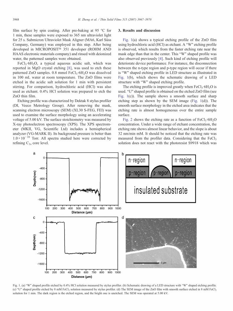
Fig. 1. (a) “W” shaped profile etched by 0.4% HCl solution measured by stylus prof(c) “U” shaped profile etched by 8 mM FeCl3 solution measured by stylus profiler. (solution for 1 min. The dark region is the etched region, and the bright one is unetc
3. Results and discussion
Fig. 1(a) shows a typical etching profile of the ZnO filmusing hydrochloric acid (HCl) as etchant. A “W” etching profileis observed, which results from the faster etching rate near themask edge than that in the center. This “W” shaped profile wasalso observed previously [4]. Such kind of etching profile willdeteriorate device performance. For instance, the disconnectionbetween the n-type region and p-type region will occur if thereis “W” shaped etching profile in LED structure as illustrated inFig. 1(b), which shows the schematic drawing of a LEDstructure with “W” shaped etching profile.
The etching profile is improved greatly when FeCl3·6H2O isused. “U” shaped profile is obtained on the etched ZnO film (seeFig. 1(c)). The sample shows a smooth surface and sharpetching step as shown by the SEM image (Fig. 1(d)). Thesmooth surface morphology in the etched area indicates that theetching rate is almost homogeneous over the entire samplesurface.
Fig. 2 shows the etching rate as a function of FeCl3·6H2Oconcentration. Under a wide range of etchant concentration, theetching rate shows almost linear behavior, and the slope is about32 nm/min mM. It should be noticed that the etching rate wasmeasured from the profiler data. Considering that the FeCl3solution does not react with the photoresist S9918 which was
iler. (b) Schematic drawing of a LED structure with “W” shaped etching profile.d) The SEM image of the ZnO film with smooth surface etched in 8 mM FeCl3hed. The SEM was operated at 5.00 kV.

Fig. 2. The relationship between the etching rate and FeCl3 concentration. Fig. 4. XPS spectrum of Fe2p peaks. Curve (a) is measured from the as-etchedsample, and curve (b) from the sample after 3 cycles of 5 min ultrasonictreatment.
3969H. Zheng et al. / Thin Solid Films 515 (2007) 3967–3970
proved already by many of our experiments, it is reasonable todetermine the etching depth simply by measuring the total depthfrom the photoresist surface to the etched surface and thethickness of the photoresist.
The effects of FeCl3·6H2O etchant on the suppression of“W” shaped profile in ZnO film can be explained qualitativelyas follows. In the FeCl3·6H2O solution, the reaction betweenZnO and etchant produces dissolvable ZnCl2 salt and Fe(OH)3deposits (though the indescriptible ferric compound may bemore complicated, it does not change our explanation). Thisreaction could be expressed as:
3ZnO þ FeCl3 þ 3H2O ¼ FeðOHÞ3↓ þ 3ZnCl2
The wet chemical etching is a very complicated process. It isaffected bymany factors such as the geometric conformation of thepattern, the microcosmic structure of the film surface, thehydromechanical parameters and so on. Here we only consider asimplemodel in terms of themass transport limit. In thismodel, thestreamline and the Reynolds number (Re) play an important role inthe formation of etching profile. During the ZnO reaction withFeCl3, the resultant deposition changes Re, then the streamline,and makes the etching profile more controllable than using acid as
Fig. 3. XPS spectrum of the ZnO etched by FeCl3 solution.
etchant [9]. In this case, the “U” shaped etching profile was readilyobtained. Recently, Harush et al. discussed the similar phenom-enon in GaN film etching process [10]. In their work, a masstransport limited model was proposed as a possible mechanism,similar to the theoretical study of the patterned growth of GaAsfilm by using metal–organic chemical vapor deposition [11].
The deposition of ferric compound on the etched ZnO surfacewas confirmed using XPS. Fig. 3 shows the XPS spectrum withenergy resolution of 1.0 eV. This spectrum was obtained from theetched ZnO film surface after removing the mask. We couldobserve aweak peak at the Fe2p core level position, but no peak forCl appears. So some Fe(OH)3 deposits did cover on the surface butthe quantity was very little. These deposits could be removed afterthree times of 5 minute ultrasonic cleaning, which was confirmedby the XPS spectrum as shown in Fig. 4, where no signal for Fe2pwas observed. An Ohmic contact with low resistance can beachieved from these samples after this treatment. The fabricationof metal electrode on this surface will be reported elsewhere.
The most advantage of our work is that the “U” shapedetching profile can be realized under a relatively wide range ofFeCl3·6H2O concentration, i.e. we could delicately control theetching rate without any change to the etching profile. Incontrast, a “U” shaped etch profile on GaN surface could beobtained only when the high etchant concentration, i.e. underhigh etching rate, was used [10]. A high etching rate, however,would give rise to a shorter etching period, and make theprocess difficult to control. This problem becomes more seriousin the fabrication of device with a multilayer structure where anaccurate control of etching depth is critical. In addition, a roughsurface caused by faster etching process would be unfavorablefor the formation of low resistance Ohmic contact.
4. Conclusion
We found a practical etching process for ZnO single crystallinefilm: etching in FeCl3·6H2O solution followed by several cyclesof ultrasonic cleaning. By using this method, “U” shaped etchingprofile was readily obtained. The etched ZnO samples show verysmooth surface morphology under different etching rates. This
3970 H. Zheng et al. / Thin Solid Films 515 (2007) 3967–3970
method does not change the electrical properties significantly andis promising for the fabrication of ZnO-based devices.
Acknowledgements
This work is financially supported by the National ScienceFoundation of China under Grant Nos. 60476044, 60376004,50532090 and the Ministry of Science and Technology of Chinaunder Grant No 2002CB613502.
References
[1] D.M. Bagnall, Y.F. Chen, Z. Zhu, T. Yao, S. Koyama, M.Y. Shen, T. Goto,Appl. Phys. Lett. 70 (1997) 2230.
[2] Z.K. Tang, G.K.L. Wong, P. Yu, M. Kawasaki, A. Ohtomo, H. Koinuma,Y. Segawa, Appl. Phys. Lett. 72 (1998) 3270.
[3] D.C. Look, Mater. Sci. Eng., B, Solid-State Mater. Adv. Technol. 80(2001) 383.
[4] H. Maki, T. Ikoma, I. Sakaguchi, N. Ohashi, H. Haneda, J. Tanaka, N.Ichinose, Thin Solid Films 411 (2002) 91.
[5] J. Fryar, E. McGlymn, M.O. Henry, A.A. Cafolla, C.J. Hanson, Physica, B340–342 (2003) 210.
[6] J. Zhu, N.W. Emanetoglu, Y. Chen, B.V. Yakshinskiy, Y. Lu, J. Electron.Mater. 33 (2004) 556.
[7] Z.X.Mei, Y.Wang, X.L. Du,M.J. Ying, Z.Q. Zeng, H. Zheng, J.F. Jia, Q.K.Xue, Z. Zhang, J. Appl. Phys. 96 (2004) 7108.
[8] K. Sangwal, J. Mater. Sci. 17 (1982) 3598.[9] L.D. Landau, E.M. Lifshitz, Fluid Mechanics, 2nd Ed. Pergamon Press,
Oxford, 1987 chapter 2.[10] E. Harush, S. Brandon, J. Salzman, Y. Paz, Semicond. Sci. Technol. 17
(2002) 510.[11] D.G. Coronell, K.F. Jensen, J. Cryst. Growth 114 (1991) 581.


![Band Bending Engineering at Organic/Inorganic Interfaces ... · has been shown to form stable (2 × 2) patterns on ZnO(1010) without inducing appreciable etching.[23–25] Moreover,](https://img.dokumen.tips/doc/110x75/5f02c9607e708231d4060152/band-bending-engineering-at-organicinorganic-interfaces-has-been-shown-to-form.jpg)