Embed Size (px)
Citation preview

Wally Dream JobWally Dream Job
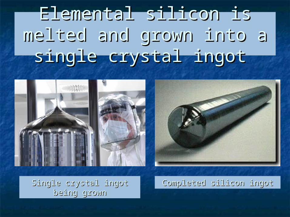
Elemental silicon is melted Elemental silicon is melted and grown into a single and grown into a single
crystal ingot crystal ingot
Single crystal ingot being Single crystal ingot being growngrown
Completed silicon ingotCompleted silicon ingot
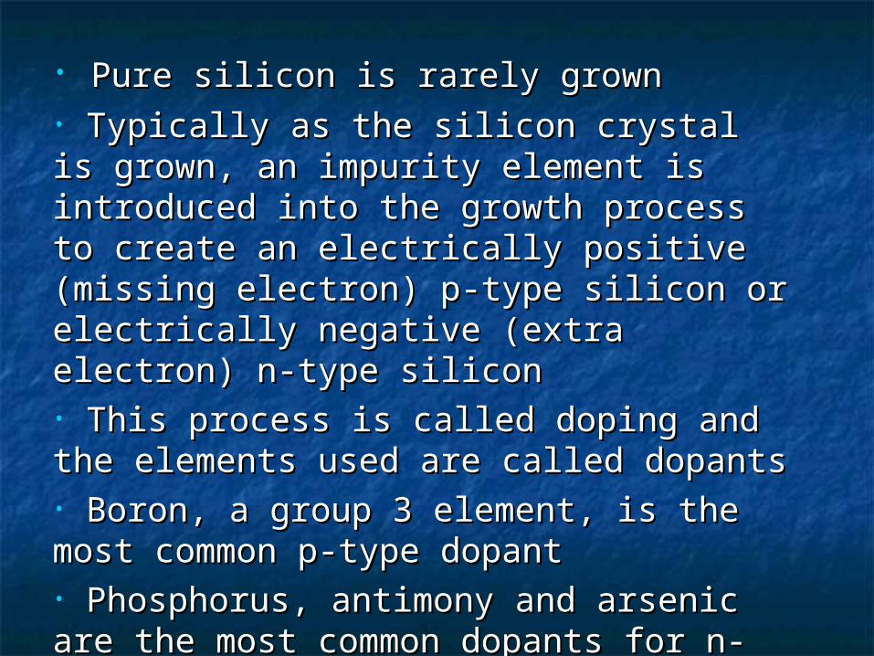
• Pure silicon is rarely grownPure silicon is rarely grown• Typically as the silicon crystal is grown, Typically as the silicon crystal is grown, an impurity element is introduced into the an impurity element is introduced into the growth process to create an electrically growth process to create an electrically positive (missing electron) p-type silicon or positive (missing electron) p-type silicon or electrically negative (extra electron) n-electrically negative (extra electron) n-type silicontype silicon• This process is called doping and the This process is called doping and the elements used are called dopantselements used are called dopants• Boron, a group 3 element, is the most Boron, a group 3 element, is the most common p-type dopantcommon p-type dopant• Phosphorus, antimony and arsenic are the Phosphorus, antimony and arsenic are the most common dopants for n-type silicon. most common dopants for n-type silicon.

SoSo Dopants are used to change the Dopants are used to change the
conductivity of the silicon crystal.conductivity of the silicon crystal. The amount of dopant introduced into the The amount of dopant introduced into the
crystal as it is being grown determines the crystal as it is being grown determines the resistivity of the silicon crystal and thus resistivity of the silicon crystal and thus the resulting wafers cut from this crystalthe resulting wafers cut from this crystal
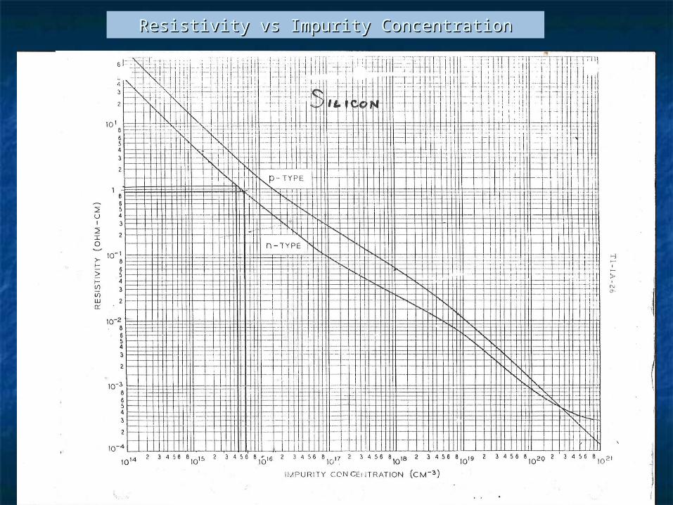
Resistivity vs Impurity ConcentrationResistivity vs Impurity Concentration
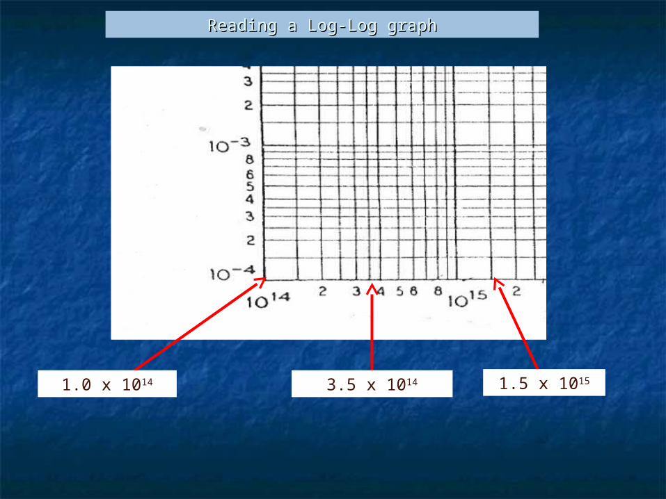
Reading a Log-Log graphReading a Log-Log graph
1.0 x 10¹⁴ 1.5 x 10153.5 x 1014
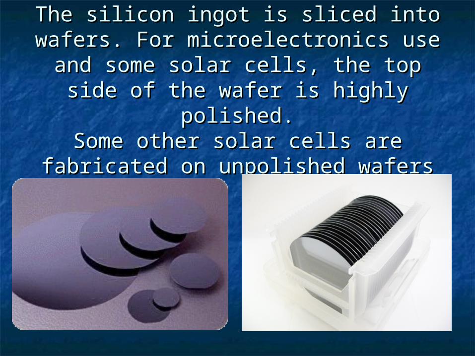
The silicon ingot is sliced into wafers. The silicon ingot is sliced into wafers. For microelectronics use and some For microelectronics use and some
solar cells, the top side of the wafer is solar cells, the top side of the wafer is highly polished.highly polished.
Some other solar cells are fabricated Some other solar cells are fabricated on unpolished waferson unpolished wafers
Junction FormationJunction Formation
Once the wafer has been created Once the wafer has been created with the appropriate dopant with the appropriate dopant (resistivity level) it is ready for (resistivity level) it is ready for additional dopant layersadditional dopant layers
Boron continues to be the most Boron continues to be the most common p-type dopant and common p-type dopant and phosphorus is now the most common phosphorus is now the most common dopant for n-type regionsdopant for n-type regions

Dopants can be introduced into Dopants can be introduced into the silicon crystal in a the silicon crystal in a
variety of waysvariety of ways
1.1. High TemperatureHigh Temperature plus time plus time1.1. Solid sourcesSolid sources
2.2. Liquid sourcesLiquid sources
3.3. Gaseous sourcesGaseous sources
2.2. Ion ImplantationIon Implantation
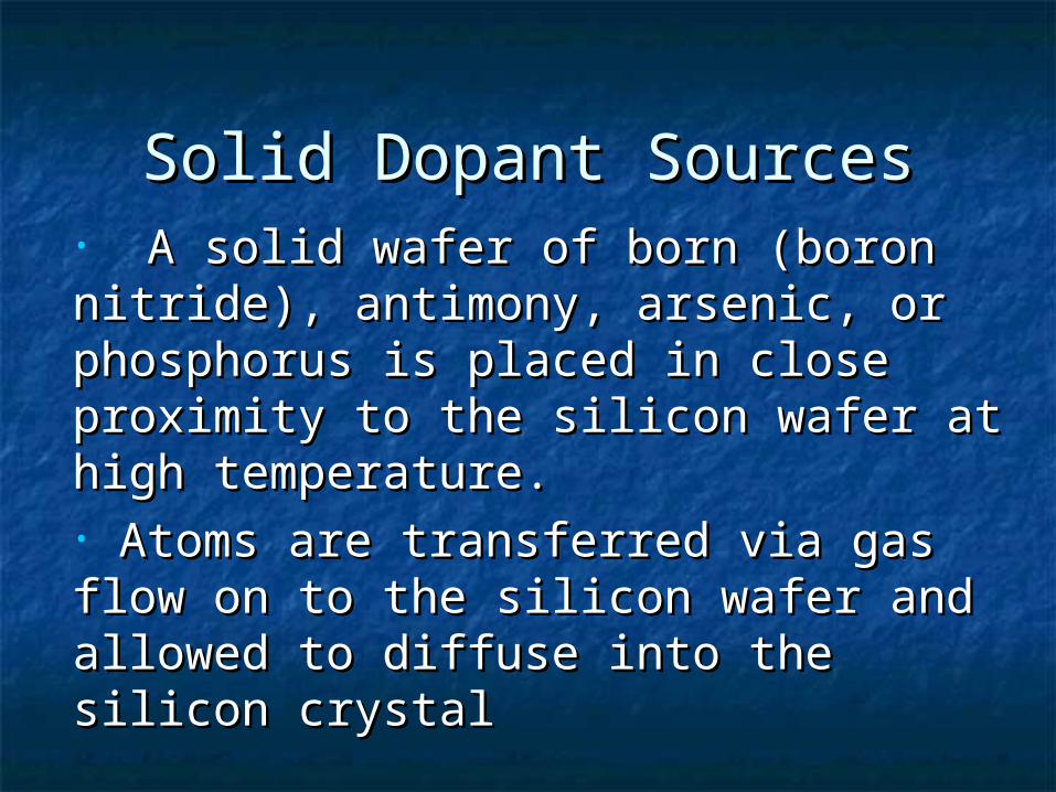
Solid Dopant SourcesSolid Dopant Sources• A solid wafer of born (boron nitride), A solid wafer of born (boron nitride), antimony, arsenic, or phosphorus is antimony, arsenic, or phosphorus is placed in close proximity to the silicon placed in close proximity to the silicon wafer at high temperature.wafer at high temperature.• Atoms are transferred via gas flow on Atoms are transferred via gas flow on to the silicon wafer and allowed to to the silicon wafer and allowed to diffuse into the silicon crystaldiffuse into the silicon crystal
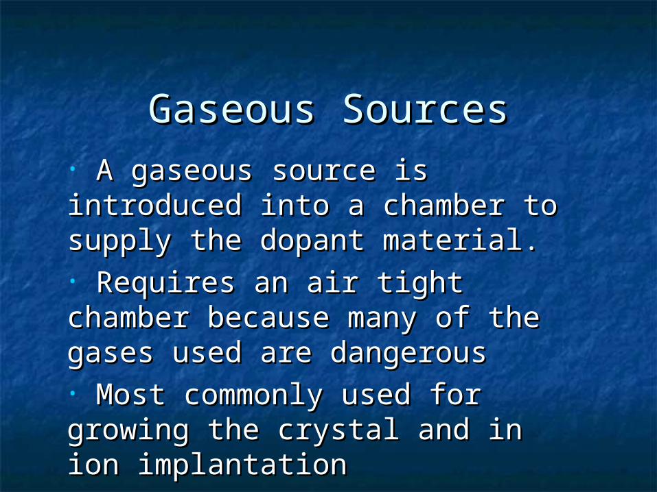
Gaseous SourcesGaseous Sources• A gaseous source is introduced A gaseous source is introduced into a chamber to supply the into a chamber to supply the dopant material. dopant material. • Requires an air tight chamber Requires an air tight chamber because many of the gases used because many of the gases used are dangerousare dangerous• Most commonly used for growing Most commonly used for growing the crystal and in ion implantationthe crystal and in ion implantation
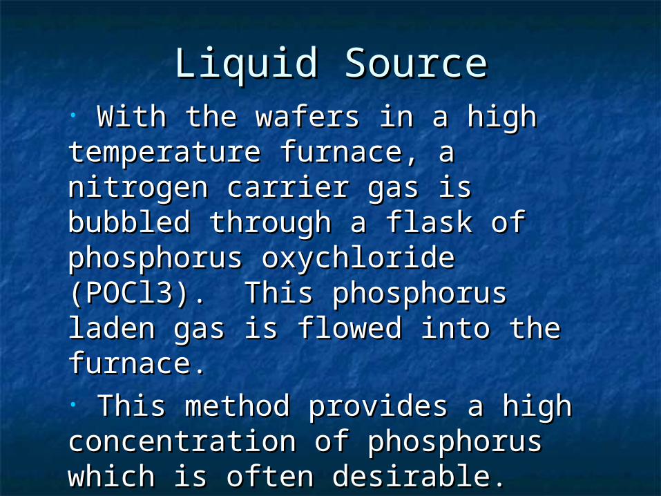
Liquid SourceLiquid Source• With the wafers in a high With the wafers in a high temperature furnace, a nitrogen temperature furnace, a nitrogen carrier gas is bubbled through a carrier gas is bubbled through a flask of phosphorus oxychloride flask of phosphorus oxychloride (POCl3). This phosphorus laden (POCl3). This phosphorus laden gas is flowed into the furnace.gas is flowed into the furnace.• This method provides a high This method provides a high concentration of phosphorus which concentration of phosphorus which is often desirable.is often desirable.• However, this chemical is toxic However, this chemical is toxic and dangerous to use and dangerous to use

Liquid SourceLiquid Source• Another liquid source is a “spin on” filmAnother liquid source is a “spin on” film• This film is spun on the wafer, like This film is spun on the wafer, like photoresist, to a uniform layerphotoresist, to a uniform layer• The wafer is then inserted into a high The wafer is then inserted into a high temperature furnace and the film is then temperature furnace and the film is then the source of dopant.the source of dopant.• Depending on time and temperature, the Depending on time and temperature, the dopant diffuses into the silicon to a certain dopant diffuses into the silicon to a certain depthdepth• This is the method we will use on our This is the method we will use on our initial solar cellinitial solar cell•
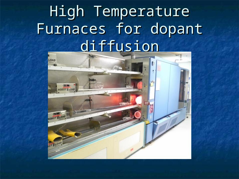
High Temperature Furnaces High Temperature Furnaces for dopant diffusionfor dopant diffusion
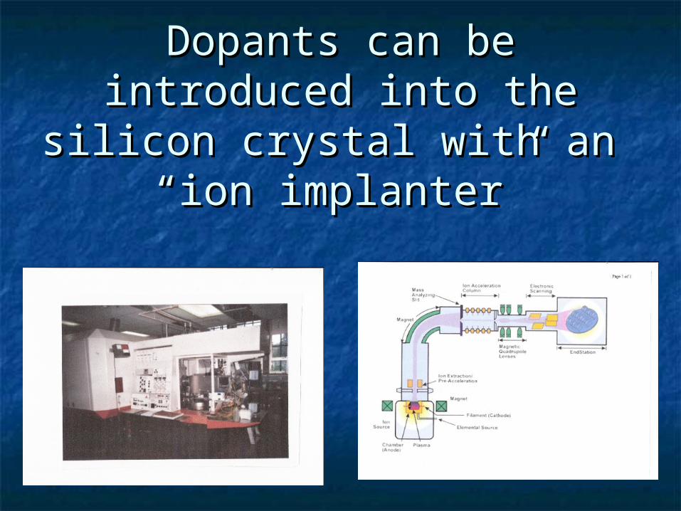
Dopants can be introduced Dopants can be introduced into the silicon crystal with into the silicon crystal with
an an “ion implanter”“ion implanter”
Ion ImplantationIon Implantation• Tool is very expensive – greater Tool is very expensive – greater than $1 millionthan $1 million• Requires high level technical Requires high level technical support, operation, and support, operation, and maintenancemaintenance• Implantation of ion causes crystal Implantation of ion causes crystal damage that needs to be damage that needs to be annealed outannealed out• Still requires a high temperature Still requires a high temperature furnace for diffusion of impuritiesfurnace for diffusion of impurities• Not a University option BUT Not a University option BUT foundries offer the service foundries offer the service
Assignment due next classAssignment due next class
Resistivity vs Concentration Resistivity vs Concentration Worksheet from the web siteWorksheet from the web site