Embed Size (px)
Citation preview

VLSI Implementation of 4×4 Mesh topology
for Network-on-chip
A Project Thesis
By
TETALA NEEL KAMAL REDDY
Department of Electronics and Communication Engineering
NATIONAL INSTITUTE OF TECHNOLOGY
ROURKELA
2012-14

VLSI Implementation of 4×4 Mesh Topology
for Network-on-Chip
A Thesis submitted in Partial Fulfillment of the requirements for the degree of
Master of Technology
In
VLSI DESIGN AND EMBEDDED SYSTEM
By
TETALA NEEL KAMAL REDDY (212EC2131)
Under the guidance of Prof. Ayas Kanta Swain
Department of Electronics and Communication Engineering
NATIONAL INSTITUTE OF TECHNOLOGY
ROURKELA
2012-14

To NIT Rourkela
and two of my best years there.

DEPARTMENT OF ELECTRONICS AND COMMUNICATION ENGINEERING
NATIONAL INSTITUTE OF TECHNOLOGY
ROURKELA
Certificate
This is to certify that the work manifested in this thesis entitled “VLSI
Implementation of 4×4 Mesh Topology for Network-on-Chip” has been carried out
by Mr. Tetala Neel Kamal Reddy in partial fulfillment of the requirements for the
award of the degree of M. Tech in VLSI Design & Embedded System in the
duration of 2012-14.
This is further certified that this thesis is an authentic work carried out
by him under my supervision and guidance and the work embodied in this
thesis, to the best of my knowledge, has not been submitted to any other
university/institute for the award of any Degree or Diploma.
Prof. Ayas Kanta Swain
Date: 2 June, 2014 Department of ECE
National Institute of Technology
Rourkela - 769008

v
ABSTRACT
Nowadays, every electronic system, ranging from a small mobile phone to a
satellite sent into space, has a System-on-Chip (SoC). Over the years, SoCs have
undergone rapid evolution and are still progressing at a swift pace. But, due to this
explosive evolution of semiconductor industry, the devices are scaling down at a rapid
rate and hence, the SoCs today have become communication-centric. However, the
existing bus architectures comprising of wires for global interconnection in SoC Designs
are undergoing a design crisis as they are not able to keep up with the rate of scaling
down of devices. In response to this crisis, Network-on-Chip (NoC) is an upcoming
archetype, and is becoming a leading contender to replace the conventional bus
architectures.
Many Network-on-Chip topologies have been introduced in an attempt to tackle
various chip architecture needs and routing techniques. A network simulator NS2 has
been utilized in an attempt to simulate the functioning of some of the topologies like
Mesh, Binary Tree, Torus and Butterfly Fat Tree (BFT). Their performances in various
traffic scenarios has been assessed and compared taking throughput, maximum end-to-
end latency and dropping probability as parameters. It can be inferred from simulation
results that with respect to throughput and dropping probability, Torus topology has an
upper hand over the others whereas BFT topology provides lower latency as compared to
others. The Mesh topology is well-suited for incorporating regular-sized processing
elements on a single chip. It is also quite simpler to design and incorporate various
routing protocols into it as opposed to others. Thus, to validate the functioning of NoC
on hardware, 4×4 Mesh architecture has been designed in VHDL and the same has been
synthesized for Virtex II Pro FPGA.

vi
ACKNOWLEDGEMENTS
First and foremost, I would like to express my sincerest appreciation to my
project guide, Prof. Ayas Kanta Swain, for his guidance and tremendous support
throughout the course of this project. His knowledge and expertise have been really
helpful in this research work. The regular discussions with him and his ideas for
approaching each problem statement in a different manner have been extremely useful.
Without his utmost help, this dissertation would not have been possible.
Next, I would like to thank Prof. K. K. Mahapatra, Prof. D. P. Acharya, Prof.
P. K. Tiwari, and Prof. M. N. Islam for their valuable advices and ideas which helped
me in thinking clearly whenever I got stuck during my project.
I would like to thank all the faculty members and non-teaching staff of the
Department of ECE for helping me directly or indirectly in completion of this project.
Next, I would like to express my thanks to all the Ph. D. and Research scholars
who have readily provided a helping hand in my time of need and acknowledged my
numerous requests without any pique regarding any technical support.
The most important people in my life are my parents and my elder brother who
have been a source of inspiration throughout my life. The discussions with them,
especially my brother, have assisted me through many a time of ordeal. I would like to
thank them from the bottom of my heart.
Away from home in a distant land, the people who constantly support and
encourage a person are his friends. I am utmost grateful to my friends, here at NIT
Rourkela. Apart from the regular education from my professors, I have learnt many
things from my friends. I would like to express my thanks to all of them for making these
two years a fantabulous journey.
NEEL KAMAL

vii
CONTENTS
ABSTRACT v
ACKNOWLEDGEMENTS vi
LIST OF FIGURES ix
LIST OF TABLES x
ABBREVIATIONS xi
1. Introduction 1
1.1 History of Interconnects and Evolution of NoCs 3
1.1.1 Buses 4
1.1.2 Crossbars: 4
1.1.3 Network-on-Chip (NoC): 5
1.2 Motivation 6
1.3 Objective 7
1.4 Organization of the Thesis 7
2. Network on Chip: A Background 9
2.1 Analogy of NoC with a Computer Network System 10
2.2 NoC Design Concepts 11
2.2.1 Switching Techniques 11
2.2.2 Routing Strategies 13
2.2.3 Flow Control 14
2.2.4 Topology 15
2.3 Performance Metrics of NoC 19
2.3.1 Throughput 20
2.3.2 Latency 20
2.3.3 Dropping Probability 20
2.3.4 Offered Traffic 21
2.4 Literature Review 21
3. NS2: Network Simulator 23
3.1 Basic Structure of NS2 24
3.2 Trace File 25
3.3 NAM (Network Animator) 26
viii
3.4 Performance Assessment of NoC Topologies using NS2 26
3.4.1 Max. End-to-end Latency v/s Traffic Load 28
3.4.2 Dropping Probability v/s Traffic Load 29
3.4.3 Average Throughput v/s Traffic Load 30
3.4.4 Node Throughput v/s Traffic Load 31
4. Implementation of 4×4 Mesh Topology for NoC in VHDL 33
4.1 Router Architecture 34
4.2 FIFO Buffer 35
4.2.1 Read/Write Logic 36
4.2.2 Block Diagram 36
4.3 Arbiter 38
4.3.1 State Diagram for Round-Robin Arbitration Logic 38
4.3.2 Block Diagram 40
4.4 Crossbar 41
4.4.1 Crossbar Connections 41
4.4.2 Block Diagram 42
5. Simulation Results 44
5.1 Device Utilization Summary 45
5.2 FIFO Buffer module 45
5.3 Arbiter module 46
5.4 Crossbar module 49
5.5 Router module 49
5.6 4×4 Mesh module 49
6. Conclusion 53
6.1 Scope of Future Work 54
BIBLIOGRAPHY 55
PUBLICATIONS 58

ix
LIST OF FIGURES
Fig. 1.1 Conventional SoC with Bus Architecture 4
Fig. 1.2 Crossbar based SoC 5
Fig. 1.3 A 3×3 Mesh NoC 6
Fig. 2.1 Example of Switching Technique (using virtual channels) 11
Fig. 2.2 XY Routing Strategy 14
Fig. 2.3 Router and Resource Nodes 16
Fig. 2.4 Mesh Topology 16
Fig. 2.5 CMesh Topology 17
Fig. 2.6 Torus Topology 17
Fig. 2.7 Folded Torus Topology 18
Fig. 2.8 Binary Tree Topology 18
Fig. 2.9 SPIN Topology 19
Fig. 2.10 BFT Topology 19
Fig. 3.1 Basic Structure of NS2 24
Fig. 3.2 Format of each trace line 25
Fig. 3.3 Sample NAM window 26
Fig. 3.4 Variation of Max End-to-end Latency with Traffic load for different topologies 28
Fig. 3.5 Variation of Dropping Probability with Traffic load for different topologies 29
Fig. 3.6 Variation of Average Throughput with Traffic load for different topologies 30
Fig. 3.7 Throughput for each node under 100% Traffic Load for different topologies 32
Fig. 4.1 4×4 Mesh Architecture 34
Fig. 4.2 Router Block Diagram 35
Fig. 4.3 FIFO Buffer Block Diagram 37
Fig. 4.4 State Diagram for Round-Robin Arbitration 39
Fig. 4.5 Block Diagram of Arbiter 40
Fig. 4.6 Block Diagram of Crossbar 43
Fig. 5.1 Simulation Waveforms of FIFO Buffer module 47
Fig. 5.2 Simulation Waveforms of Arbiter module 48
Fig. 5.3 Simulation Waveforms of Crossbar module 50
Fig. 5.4 Simulation Waveforms of Router module 51
Fig. 5.5 Simulation Waveforms of 4×4 Mesh module 52

x
LIST OF TABLES
Table 3.1 Constraints Applied in NS2 to simulate NoCs 27
Table 3.2 Max. End-to-end Latency v/s Load 28
Table 3.3 Dropping Probability v/s Load 29
Table 3.4 Average Throughput v/s Load 30
Table 3.5 Node Throughput at each target node 31
Table 4.1 Crossbar connections between inport demuxes and outport muxes 42
Table 5.1 FPGA Device Utilization Summary 45

xi
ABBREVIATIONS
SoC System-on-Chip
NoC Network-on-Chip
NS2 Network Simulator Version 2
BFT Butterfly Fat Tree
VHDL VHSIC Hardware Description Language
VHSIC Very High Speed Integrated Circuit
FPGA Field Programmable Gate Array
NAM Network AniMator
FIFO First In First Out
CMesh Concentrated Mesh
SPIN Scalable Programmable Integrated Network
MtM More than Moore
GALS Globally Asynchronous and Locally Synchronous
DRAM Dynamic Random Access Memory
DSP Digital Signal Processing
ASIC Application Specific Integrated Circuit
CLB Configurable Logic Block
IP Intellectual Property
PDA Personal Digital Assistant
TCP Transmission Control Protocol
TCL Tool Command Language
AWK Aho, Weinberger, Kernighan
SFQ Stochastic Fairness Queuing
CBR Constant Bit Rate
LUT Look Up Table
IOB Input/output Block
GCLK Global Clock

Chapter One
Introduction

2
In today‟s world, the core of every electronic system, from a mobile phone to a
missile control system, from a remote controlled toy car to a spacecraft etc., is a System
on Chip (SoC). A SoC is an on-chip incorporation of an assortment of functional
hardware blocks to ensemble a specific product application. SoC designs offer unified
explanations to demanding design complications in the multimedia, consumer
electronics, and telecommunications areas. A large factor in the improvement in these
fields is dependent on the designers‟ talent in apprehending multifaceted electronic
engines in acute “time to market” burden. Several factors have been responsible for the
rapidly undergoing evolution of systems architectures in the SoC domain. These factors
[1] are:
In the present day, there is a requirement for convergence of various applications
(Video, Communication, Computing and etc.) onto a single IC. Generally, when any of
these applications are used in a stand-alone fashion, they have resources which are
secluded and handcrafted to them. But now, these applications would have to share some
of these secluded resources in order to harmoniously function as a unit on integration
onto a SoC, for example from a Quality of Service viewpoint.
Moore‟s Law of semiconductor logic and memory products is propelling the
blazing scale of integration of numerous IP Cores in a single chip. Moreover, due to
Moore‟s Law, many other technologies have advanced, even though at a gentler pace.
Due to these technologies becoming accessible, many new abilities are now coming up
as per the “More than Moore” (MtM) approach [2]. These developments are further
resulting in the tremendous growth of SoCs.
The developments in the silicon processes of chip fabrication have helped in the
scaling of transistors, which help advancement in system architectures for SoC design.

3
With swelling intricacy of systems and developments in technology, the pins and
wires that manage interconnections amongst systems‟ components are scaling down at a
slower rate than the components. Moreover, synchronization of forthcoming chips with a
solitary clock and insignificant distortion will be exceedingly challenging. The most
likely solution of this synchronization prototype for forthcoming chips could be Globally
Asynchronous and Locally Synchronous (GALS) that comprises use of numerous
different clocks [3]. Transfer of data between resources rather than logic, is becoming
the limiting factor concerning cost, performance, size, and power in these systems.
Moreover, the frequency of communication amongst components is quite lower than the
clock frequencies of recent processors. These factors combine for System-on-Chips
swiftly becoming communication oriented.
But, there have been difficulties in the scaling of wires at the same rate as
transistors and hence gates are costing comparatively less than wires, both from an area
and performance viewpoint, than some years ago. Due to this factor, the busses,
employed in SoC designs which have long been the backbone of system interconnects,
are getting inept at keeping up with increasing system performance requirements. There
have been many developments in the area of system interconnects like crossbars etc.,
which provide a solution to this communication predicament.
1.1 History of Interconnects and Evolution of NoCs
Looking back at the history of SoC-interconnect technology, the semiconductor
industry conventionally trailed in looking at the advancement of the system from a
communication perspective that links a chip‟s individual components amongst one
another within the chip. The history of on-chip interconnects has three phases [4]:

4
1.1.1 Buses
The first phase was dominated by buses. A processor could send data to or
retrieve data from a DRAM memory and other target peripherals as per requirement, by
performing read and write operations on bus. Eventually, other sources started using the
bus, and when a source uses the bus, other sources cannot use that bus and have to wait
for their turn. Thus, arbiters became essential to alternately award different sources the
bus to access their requested targets. Due to this, data transfer gets delayed and thus
overall performance of the system gets lowered. This problem led to the development of
multi-bus architectures. But even these architectures could not prevent data delay and
moreover throughput was also getting affected. A conventional SoC with shared-bus
architecture has been displayed in Fig. 1.1.
Fig. 1.1 Conventional SoC with Bus Architecture
1.1.2 Crossbars:
The beginning of the integration of numerous cores onto chips led to many
sources trying to access different targets concurrently that created bottlenecks on the bus.
To solve this problem, crossbars came into the picture. The benefit of using crossbars
instead of buses is that links amongst sources and targets communicate concurrently and
hence parallel data transfer is possible which improves system performance. A SoC with
Crossbar based interconnect is shown in Fig. 1.2. However, crossbars would need

5
intricate control logic to create links between numerous sources and targets and facilitate
exchanges. Besides, a crossbar interconnect architecture has a very high hardware
requirement. For example, implementing a 928x928 crossbar in FPGA would require
approximately 53,824 CLBs for each input [5].
Fig. 1.2 Crossbar based SoC
1.1.3 Network-on-Chip (NoC):
As SoCs grew in quantity of IP cores, bus architectures and crossbars were
exposed of their deficiencies. Shared bus architectures led to resource contention and
hierarchical bus architectures and crossbar designs generated complexity.
Interconnection networks offer an attractive solution to this communication predicament
and are becoming persistent in SoC systems. A well-designed interconnection network
makes a well-organized use of limited communication means while providing low-
latency, high bandwidth communication amongst different IPs with a minimum cost and
low energy-dissipation. Undeniably, as system density and integration continued
increasing, quite many designers discovered that it is more efficient to route packets, not
wires. Utilizing an interconnection network in a SoC than a dedicated wiring permits

6
limited bandwidth to be shared so that it can be used resourcefully. In contrast, dedicated
wiring is idle mostly. Using a network also administers regular, organized use of
communication resources, making SoCs easier to design, repair, and optimize. Fig. 1.3
displays a 3×3 Mesh topology for NoC.
Fig. 1.3 A 3×3 Mesh NoC
Packet-based Network-on-Chip (NoC) has arisen as a remedy to the SoC design
problem from a communication centric viewpoint. Moreover, arranging the interconnect
logic uniformly throughout the chip rather than having buses as junction points has
greatly eased floor planning of high-density chips. From a research point of view,
implementation of a NoC on FPGA plays an important role in its design validation and
performance assessment. This design must fulfill quality-of-service essentials such as
performance, consistency and energy boundaries.
1.2 Motivation
SoC designs are undergoing large-scale functional integration and there has been
a rapid evolution in the field of technological advancements in semiconductor design.
This has allowed many functions to be added to existing SoC systems making them more
sophisticated, smaller, less power-dissipating and more cost-effective. But, the

7
interconnect technology in SoC designs has not been receiving the development focus
that processing elements are getting.
Network-on-Chip is the latest paradigm in interconnect technology which has
several advantages over its predecessors. It has been an active area for research for over
a decade and still many new NoC concepts are being developed on a regular basis. The
Mesh topology for NoC has been an important area of focus for researchers as its
structure is simpler and it can incorporate regular-sized processing elements easily.
1.3 Objective
To develop a lucid understanding of the various concepts of NoC to carry out
design of a NoC in a well-planned manner.
To get acquainted with a network simulator like NS2 and the various tools it
provides for evaluation of networks.
To perform assessment of various topologies in terms of networks metrics in
NS2.
To implement a well-chosen topology for NoC and validate its functionality in
VHDL.
1.4 Organization of the Thesis
The approach of this thesis is to describe the various concepts of NoC followed
by its simulation in NS2 and implementation in VHDL. The thesis is systematized as
follows:
Chapter 1 includes the motivation behind this dissertation and the various
objectives achieved in the course of this project.

8
Chapter 2 discusses the idea of NoC in detail with emphasis on its topology
concept and its performance assessment methods. The chapter is ended with a literature
review on the concerned area.
Chapter 3 introduces the network simulator NS2 and its various features. It
discusses the performance assessment of various topologies in terms of the parameters
pointed out in chapter 2.
Chapter 4 presents the implementation of a 4×4 Mesh NoC with detailed
description of the functioning of each of its blocks.
Chapter 5 discusses the simulation results of the various blocks of 4×4 Mesh NoC
as obtained in Xilinx ISE simulator.
Chapter 6 concludes the contribution of the thesis and gives a brief view into the
scope of the future work in this area.

Chapter Two
Network on Chip: A Background

10
Network-on-chip (NoC) is becoming an upcoming archetype for communications
within a System-on-Chip (SoC). Different modules such as general processor, DSPs,
memories and dedicated IP cores transfer data amongst each other using NoC as an open
transportation system. NoC comprises of numerous routers interconnected by point-to-
point connections for data transfer, such that data packets can be transmitted from a
source unit to any target unit across several connections, while taking routing choices at
routers. These choices or algorithms are formulated so as to achieve large parallelism
and utilize NoC fully to its potential. A NoC is comparable to a telecom network that
employs packet switching across multiplexed links. There have also been many NoC
schemes that could utilize circuit-switching techniques.
2.1 Analogy of NoC with a Computer Network System
The basic concepts behind the approach of a Network-on-Chip (NoC) can be
derived from the computer network model. A NoC and a computer network are quite
similar in the logic that both have processing elements, routers, connections between
processing elements to routers and between routers to routers, data forwarding
mechanism, routing approaches and protocols and finally data transferred in the form of
packets. However, there are quite many differences between the two, the primary one
being the size, computer networks can vary from being limited in a room to an entire
metropolitan and can even be spread over the entire world as the Internet whereas a NoC
is mostly designed to fit within a 30-40 nm silicon die or even smaller. In a NoC, storage
and processing resources are arranged tightly than in networks. Implementing memory
on-chip is quite expensive considering the area it occupies. Hence on-chip, only
restricted buffers can be employed [6]. In NoC, computation also gets costly. Since
NoCs are designed to be embedded into handy devices like PDA's or mobiles, power is

11
also only of the chief issues. Thus, complicated processing logic and inter-
communication structures are impractical for NoCs in order to avoid excessive power
consumption.
2.2 NoC Design Concepts
The functionality of a NoC is defined by how the network arranges the and how
data is transported from an origin to a target through the network. These concepts are
required to be considered when designing a NoC. These NoC design concepts can be
categorized as switching techniques, routing strategies, flow control, topology etc.
2.2.1 Switching Techniques
The way in which the internal switches are to be set so as to connect the inputs of
a router to its outputs is defined by switching methodology. This also explains at which
time the data may be transmitted across this created path [7]. NoC initially employed
techniques that are generally utilized in communication networks i.e., circuit and packet
switching. But, these techniques were not suitable for the low-latency requirements of
NoC for parallel processing. In NoC, the realized switching technique is mostly
responsible for its packet latency. Fig. 2.1 shows an example of switching decision using
virtual channels.
Fig. 2.1 Example of Switching Technique (using virtual channels)

12
Some of the existing switching techniques are
Circuit Switching: In this, the data is transmitter between the origin and the target
only after the path has been established between the two.
Packet Switching (Store and forward): Unlike circuit switching, a complete path
between origin and target is not essential for transmitting of data. Whenever, a
path is available between two routers, a complete packet can traverse that path.
Due to this, this switching delivers a greater delay as a packet can only be
transmitted to the next router if it is entirely present at the present router.
Moreover, large buffers with sizes of at least one packet are to be provided at
each router. Although, this switching assures consistent data transfer but the
resources of NoC are not properly utilized.
Virtual Cut-through Switching: In this type of switching, if the intended output
channel of a router is free and the header of a data packet arrives, it immediately
starts forwarding the packet. The router need not wait for the arrival of the entire
packet. But if the intended output channel is in use, then the entire packet has to
be stored and hence, similar to packet switching, the buffer constraint here too is
of at least one packet.
Wormhole Switching: In this case, each packet is allocated into reduced sizes
called flits which are flow control digits. These flits can be broadly classified into
head, body and end flits. The control and routing report of a data packet is
contained in the head flit. The main data or payload is present in the body flit and
the end flit can contain remaining payload in addition to packet end information.
This greatly reduces the size of buffers which can be as small as one flit.

13
2.2.2 Routing Strategies
The path that is to be traversed by a data packet when transmitted from a source
to a destination terminal is defined by a routing strategy. Depending on the topology of
the network, there could either only a single path or multiple paths from each source to
target terminal [8]. The purpose of a good routing strategy is to provide such a path for
data so as to balance the load uniformly across channels irrespective of how the traffic
pattern is going to be. A NoC topology can be considered analogous to a roadways
system, which has been described in Section 2.2.4. Considering this analogy, it can be
said that topology explains the roadmap along with the roads and junctions and the
routing method helps in directing the car on the road by taking decisions at each junction
on the direction of turn. Hence, similar to avoid getting stuck in traffic, it is essential to
balance the load of the network across different channels rather than congesting a single
channel.
The Routing Strategies have to be such that there must be no occurrence of
livelock, deadlock and starvation situations [9].
Livelock occurs when the packets are continuously moving around in the network
without any headway towards the target.
When a condition is reached where different routers are waiting for access to
resources which have not yet been released by the other router, no forward occurs
and this condition is defined as deadlock.
Suppose an out channel is constantly allocated to a packet, and some other packet
in the buffer needs this channel, this packet gets blocked and a condition called
starvation occurs.

14
Routing Strategy can be categorized into deterministic or adaptive based on how
they define a path.
In deterministic routing, the path for a particular set of source and target is
predefined and is constant throughout the lifetime of the NoC.
Adaptive routing defines a path at runtime based on the immediate traffic
scenario of the network. This type of routing provides numerous paths for a data
packet from the source to target.
Routing can be more clearly elucidated with the help of an example of XY-
routing. In this, the packets are first directed along X line till they reach the y-coordinate
of the target, and afterwards along Y line, as shown in Fig. 2.2. If in between, some
channel between two routers is in use by some other packet, the former packet has to
wait in the buffer of the router until the channel is free.
Fig. 2.2 XY Routing Strategy
2.2.3 Flow Control
When packets are traversing on a path, the granting of resources to them is
managed by the concept known as Flow Control [8]. With reference to NoC, the most
essential resources are channels and buffers in routers. Buffers are responsible for
providing temporary storage to packets when they are waiting in a router for a channel to

15
traverse to the next router. As per the analogy with the roadways system, the flow control
concept is similar to traffic lights on the road which determine when a car can move on
to the next road or whether it should wait in line for the road to clear. To perfectly utilize
a NoC, this concept must avoid conflicts with respect to resources that can hold a
channel free. In other words, if a packet is waiting on a buffer behind a packet waiting
for a busy channel, it should not be blocked if it needs to go onto an idle channel. A good
flow control strategy is fair and avoids deadlock. An unfair flow control strategy can
cause a packet to wait indefinitely.
2.2.4 Topology
A NoC is implemented by connecting a collection of shared routers with the help
of shared channels. NoC topology defines the organization of these routers and channels
[8]. Continuing our roadways analogy, he channels are comparable to roads, data packets
to cars and routers to intersections on roads. A data packet can be transferred on the
channels through several hops of routers from the source to the target terminal. An
appreciable topology utilizes the features of the existing packaging technology to satisfy
the latency and bandwidth stipulations of an implementation at minimal cost. In
designing a NoC, the paramount step is to select a topology as the other concepts such as
flow control and routing strategy comprehensively depend on topology [8]. Selecting a
good topology should be based on fitting the requirements of the network to the available
packaging technology. For a variety of reasons, a special purpose network topology is
usually a bad idea. A problem-specific network often does not map well to available
packaging technology, requiring long wires or a high node degree. It is always better to
use a good general purpose topology than to design a network with a topology matched
to the problem.
16
No one topology is optimal for all applications. Different topologies are
appropriate for different constraints and requirements. The basic NoC topologies are
Mesh, Torus, Ring, Binary Tree etc. Some topologies have also been derived by
combining 2 or more of these basic topologies. Some of the various NoC topologies that
have evolved over the years are described below. In each of the corresponding diagrams,
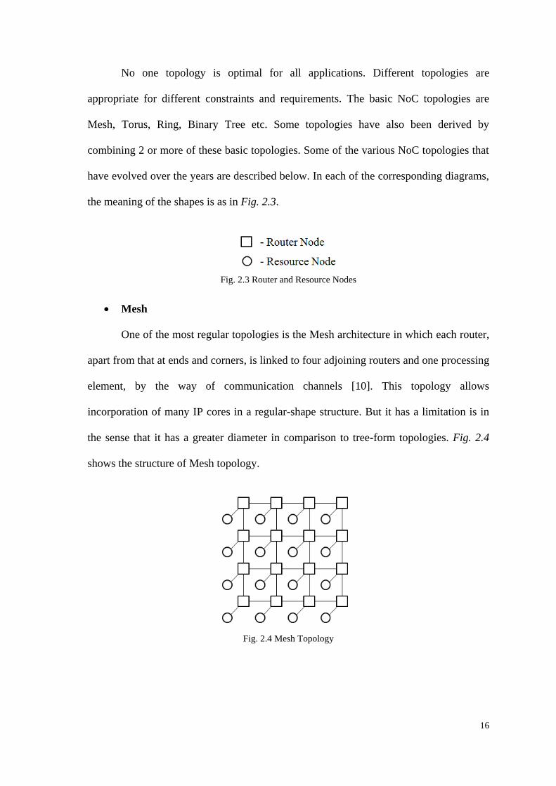
the meaning of the shapes is as in Fig. 2.3.
Fig. 2.3 Router and Resource Nodes
Mesh
One of the most regular topologies is the Mesh architecture in which each router,
apart from that at ends and corners, is linked to four adjoining routers and one processing
element, by the way of communication channels [10]. This topology allows
incorporation of many IP cores in a regular-shape structure. But it has a limitation is in
the sense that it has a greater diameter in comparison to tree-form topologies. Fig. 2.4
shows the structure of Mesh topology.
Fig. 2.4 Mesh Topology

17
Concentrated Mesh
Concentrated Mesh (CMesh) Topology was proposed to reduce diameter of mesh
by connecting four cores to a single router [11]. The limitation with this topology is that
it required long links and connectivity of each router i.e., the number of cores and
adjacent routers connected to a router, increases due to which the frequency of the router
decreases. Arrangement of nodes in CMesh is illustrated in Fig. 2.5.
Fig. 2.5 CMesh Topology
Torus
The Torus architecture [12] is fundamentally similar to a mesh except that routers
at edges are linked to routers that are situated at their opposite edge through folded
connections as shown in Fig. 2.6. Each router has five ports, one linked to an IP core and
the remaining linked to adjacent routers. The long fold-around connections may generate
excessive delays. This topology solves the problem of mesh‟s large diameter but
excessive delay is generated due to long end-around connections.
Fig. 2.6 Torus Topology

18
Folded Torus
The Folded Torus topology is obtained by folding the Torus topology [13], as
illustrated in Fig. 2.7. This folding reduces the excessive delay obtained in the torus
topology.
Fig. 2.7 Folded Torus Topology
Binary Tree
In a Binary Tree topology [14], the design is sculpted similar to a tree. A set of
coordinates (level, position) can be used to represent each node, where level is the
vertical level of the tree and position is the horizontal placing in left to right ordering.
Here, as depicted in Fig 2.8, each router node is linked to 2 nodes in the subsequent level
with all the resource nodes present at the bottommost vertical level. The limitation of this
topology is that it has small bisection width.
Fig. 2.8 Binary Tree Topology
SPIN
SPIN stands for Scalable Programmable Integrated Network [15]. It is a tree-
based generic interconnect topology which was proposed to solve the bisection width
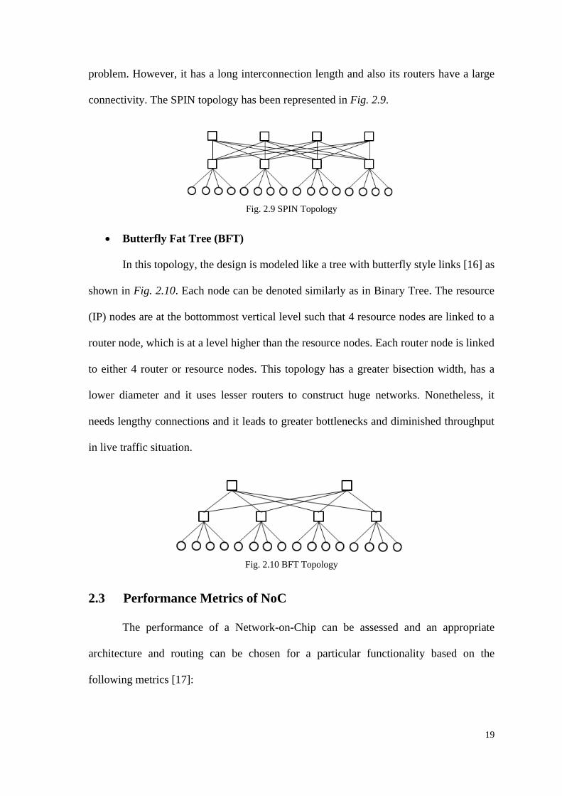
19
problem. However, it has a long interconnection length and also its routers have a large
connectivity. The SPIN topology has been represented in Fig. 2.9.
Fig. 2.9 SPIN Topology
Butterfly Fat Tree (BFT)
In this topology, the design is modeled like a tree with butterfly style links [16] as
shown in Fig. 2.10. Each node can be denoted similarly as in Binary Tree. The resource
(IP) nodes are at the bottommost vertical level such that 4 resource nodes are linked to a
router node, which is at a level higher than the resource nodes. Each router node is linked
to either 4 router or resource nodes. This topology has a greater bisection width, has a
lower diameter and it uses lesser routers to construct huge networks. Nonetheless, it
needs lengthy connections and it leads to greater bottlenecks and diminished throughput
in live traffic situation.
Fig. 2.10 BFT Topology
2.3 Performance Metrics of NoC
The performance of a Network-on-Chip can be assessed and an appropriate
architecture and routing can be chosen for a particular functionality based on the
following metrics [17]:

20
2.3.1 Throughput
The throughput of a NoC defines the rate at which data packets can traverse from
source to target terminal. The throughput, T, can be defined as follows:
( ) ( )
( ) ( ) -- Eq. 1
where Total Data Packets Received means the no. of data packets that have
reached their target terminal in full, Data Packet Length can be measured in bits or flits,
No. of IP Cores is the no. of active IPs that are participating in the traffic scenario, and
Total Active time is the total time measured from the incidence of the first packet
inception to the last packet reception. Thus, throughput gives a measure of the active part
of the maximum load that the network can handle.
2.3.2 Latency
The time measured from the start of the injection of a packet header into the NoC
at the source to the end of reception of the tail of the packet at the target. The packets
traverse through a route comprising of routers and channels in order to arrive at target
terminal from the origin. Each packet may have a diverse latency depending on their
source/target addresses and the routing strategy.
2.3.3 Dropping Probability
It is given by the ratio of the packets dropped when traversing in a topology to
the total packets sent by the source nodes in that topology. A topology with a Dropping
Probability with a value of „0‟ suggests that no packets get dropped, 100 would imply
that all packets are dropped.

21
2.3.4 Offered Traffic
It refers to the average amount of traffic generated by each source terminal of the
NoC. Generally, the above discussed metrics are calculated with offered traffic as the
independent variable.
A NoC topology is said to be productive if high throughput and low latency are
achieved and it consumes lesser energy and provided smaller area overhead.
Furthermore, NoC topologies that have smaller diameter, lesser mean distance, smaller
node degree, greater bisection width and lesser connectivity of their routers are
preferable. But, these constraints are interlinked and are a trade-off to one another.
2.4 Literature Review
With the advancement in SoC designs, researchers have been looking for a
substitute to bus-based interconnect communication.
Network on a chip (NoC) paradigm and its related procedures was presented by
Ahmed Hemani et al. in [18]. The paper introduces NoC concept as a solution to the
design problem of bus-based interconnects. A honeycomb structure, a palpable topology
for NoC has also been proposed and explicated.
Dally and Towles in [12] discussed the importance of using interconnection
networks instead of global wiring. They also drafted a network and conferred the
challenges involved in designing the architecture for such networks.
For performance assessment of NoCs, the area in most of the works that have
been done or are being pursued is based on simulation. Generally, for simulation of NoC
functionality, NS2 is the most sought after simulator even though it is suitable for
computer network related research.

22
In the paper [19], the authors, Ngo and Choi, introduced network topologies for
on-chip interconnections and utilized the NS2 software for assessing their performances
in terms of buffer size, routing strategy and routing algorithm. Muhammad Ali et al. in
[6] designed a model of fault tolerant protocol for NoC and used the simulator NS2 to
simulate it.
Many researchers are pursuing the idea of designing a NoC in FPGA and
assessing their performance on hardware with respect to bus-based designs.
Pereira & Zeferino in their paper described synthesizable cores for generation of
traffic for assessing NoC performances in FPGA [20]. In paper [21], the authors,
Shrivastava and Pandit, conferred on the analytical design of on-chip router and its
architectural implementation for MPSoC.
Wang et al. [22] proposed a flexible and fast architecture for FPGA-based NoC
simulation. In this, they virtualized NoC by plotting its modules to a simulator and
implemented DART on a Virtex II Pro FPGA.
In this dissertation, performance assessment of different topologies for NoC has
been done and a 4×4 Mesh topology for NoC has been designed using VHDL and
implemented in Virtex II Pro FPGA. These will be discussed in further sections.
Chapter Three
NS2: Network Simulator

24
NS2 [23] is an object-oriented open-source distinct event network simulator
developed at UC Berkeley and intended explicitly for exploration in computer
communication networks. It is suitable for packet switched networking. NS2 has been
developed in two languages. C++ is utilized for thorough executions of procedures like
TCP or any tailored ones. TCL scripting, alternatively, is the front-end interpreter for
NS-2 designed for creating configuration interfaces and commands [24]. NS2 contains a
bundle of tools that helps in simulating the behavior of networks. It can be used to create
different network topologies, which can be simulated under a traffic load to generate a
log of events regarding the transfer of packets from one node to another.
3.1 Basic Structure of NS2
The basic structure of NS2 is as shown in Fig 3.1. Users can execute NS2 with
the help of “ns” command to which name of the Tcl scripting file is given as input. After
execution of the Tcl file through NS2, the output is mostly a simulation trace file. On
simulation of this trace, the simulation outputs provided by NS2 are either in text format
or animation format. These outputs can be read interactively and graphically with the
help of tools such as NAM and XGraph. Furthermore, in order to understand a specific
behavior of a network, an appropriate part of the trace file generated after execution can
be extracted and transformed into a more comprehensible format.
Fig. 3.1 Basic Structure of NS2

25
NS2 provides two tools for processing data post simulation:
3.2 Trace File
NS2 generates a packet tracing file in text format that contains the properties of
every packet that passes through various nodes in the network.
Each line in a trace file is made up of 12 fields as shown in Fig. 3.2.
Fig. 3.2 Format of each trace line
The first field is type identifier which can be one of four values depending on
events experienced by a packet i.e. r (received), d (dropped), + (enqueued) and –
(dequeued). The next field gives the time at which one of above specified event
transpires. The third and fourth fields contain the source and target nodes of the
connection at which the specified event occurs. The next two fields give the name and
size of the packet respectively. If any irregular behavior of a packet occurs, it is
exhibited in the form of flags in seventh field. Next is the flow ID of packet. The source
and target addresses are specified by fields 9 and 10 respectively. The next field contains
a sequence no. for packets so as to gather the packets at the target in the correct order.
The last field contains a unique ID of packet for keeping record of all packets. Using
AWK language [25], which is an interpreted programming language designed for text
processing, these trace file or log events can be assessed to comprehend the network
behavior.

26
3.3 NAM (Network Animator)
NS2 also generates a NAM trace that registers simulation features into a text file.
This file can be converted into animation by replaying the simulation. NAM provides
many skins for visualization. These skins can be for animating flow of various colored
packets, positioning of nodes, coloring a precise connection, changing the shape of nodes
and queue observing etc. Fig. 3.3 shows a sample NAM window animating a topology
with 5 nodes.
Fig. 3.3 Sample NAM window
3.4 Performance Assessment of NoC Topologies using NS2
NS2 can be used for observing the performance metrics of a NoC topology owing
to the similarities between a NoC and a computer network as explained in Section 2.1.
For understanding the behavior of a NoC topology under various traffic constraints, a
4×4 Mesh, 4×4 Torus, Binary tree, Butterfly Fat Tree (BFT) topologies were simulated.
In this experimentation, each resource node, represented by a circle, has been connected
27
to a router node, represented by a square and the latter are interconnected as per the
topology as shown in figures Fig. 2.4, Fig. 2.6, Fig. 2.8 and Fig. 2.10. Various
constraints applied in NS2 to simulate NoCs are provided in Table I.
NoC Model Parameters Parameter Constraints
applied in NS2
Number of Resource (IP) Nodes 16
Connections Resource-Router, Router-Router
Transmission Protocols User Datagram Protocol (UDP)
Routing Scheme Static
Routing Protocol Shortest Path
Queue Mechanism Stochastic Fairness Queuing (SFQ)
Link Queue 8 packets
Bisection Bandwidth (Max.) Router-to-router – 300Mb
Resource-to-router – 200Mb
Traffic Generation Constant Bit Rate (CBR)
Traffic Rate 180 Mb
Packet Size 16 bytes
Table 3.1 Constraints Applied in NS2 to simulate NoCs
Some of the performance metrics of NoC as explained in Section 2.3 like Max.
End-to-End Latency, Dropping Probability and Throughput are evaluated for assessing
the performance of the aforementioned topologies. The results of the metrics are in the
following section.
28
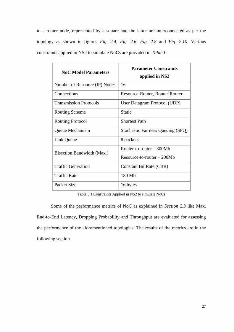
3.4.1 Max. End-to-end Latency v/s Traffic Load
The Max End-to-end Latency is calculated by taking the average of the time
taken for packets to traverse the longest distance in each topology under different traffic
load conditions.
Max. End-to-end Latency (µs)
Load 4×4
Mesh
4×4
Torus
Binary
Tree
Butterfly
Fat Tree
25% 803.844 802.133 811.562 409.855
50% 803.844 802.133 814.86 410.609
75% 803.844 802.133 831.667 412.29
100% 811.253 802.133 833.29 413.298
Table 3.2 Max. End-to-end Latency v/s Load
Table 3.2 shows the variation of Max End-to-end Latency for each topology.
These observations have been exemplified in graphical form in Fig. 3.4.
Fig. 3.4 Variation of Max End-to-end Latency with Traffic load for different topologies
350
450
550
650
750
850
25% 50% 75% 100%
Ma
x. E
nd
-to
-En
d L
ate
ncy
(µ
s)
Traffic Load
4×4 Mesh
4×4 Torus
Binary Tree
Butterfly Fat Tree

29
3.4.2 Dropping Probability v/s Traffic Load
In NS2, dropping probability is obtained by calculating the ratio of the count of
packets having type identifier “d” to the count of total number of packets generated from
each source node.
Dropping Probability
Load 4×4
Mesh
4×4
Torus
Binary
Tree
Butterfly
Fat Tree
25% 0 0 0.078 0.078
50% 0.0605 0 0.161 0.141
75% 0.082 0.049 0.456 0.376
100% 0.156 0.054 0.537 0.483
Table 3.3 Dropping Probability v/s Load
The variation of Dropping Probability with Traffic Load has been tabulated in
Table 3.3 and the graphs obtained from the same are displayed in Fig. 3.5.
Fig. 3.5 Variation of Dropping Probability with Traffic load for different topologies
0
0.1
0.2
0.3
0.4
0.5
0.6
25% 50% 75% 100%
Dro
pp
ing
Pro
ba
bil
ity
Traffic Load
4×4 Mesh
4×4 Torus
Binary Tree
Butterfly Fat Tree

30
3.4.3 Average Throughput v/s Traffic Load
Average throughput of a topology is defined as an average of number of packets
received by all the target nodes in unit time.
Average Throughput (Mbps)
Load 4×4
Mesh
4×4
Torus
Binary
Tree
Butterfly
Fat Tree
25% 36.252 36.252 33.412 33.412
50% 66.09 70.345 59.039 60.455
75% 101.603 104.685 60.197 69.092
100% 116.876 131.726 64.168 71.565
Table 3.4 Average Throughput v/s Load
Table 3.4 shows the variation of Max End-to-end Latency for each topology.
These observations have been illustrated in graphical form in Fig. 3.6.
Fig. 3.6 Variation of Average Throughput with Traffic load for different topologies
0
20
40
60
80
100
120
140
25% 50% 75% 100%
Av
era
ge
Th
rou
gh
pu
t (M
bp
s)
Traffic Load
4×4 Mesh
4×4 Torus
Binary Tree
Butterfly Fat Tree

31
3.4.4 Node Throughput v/s Traffic Load
In this experiment, 100 % traffic load is considered that indicates that all sources
are transmitting packets and under this condition, the throughput at each target node was
observed and charted in Table 3.5.
Node Throughput (Mbps)
Nodes 4×4
Mesh
4×4
Torus
Binary
Tree
Butterfly
Fat Tree
0 82.199 115.56 115.927 138.644
1 82.196 118.64 48 59.352
2 115.561 117.095 79.2898 59.987
3 117.095 117.095 48.972 60.362
4 138.644 138.644 48.007 58.737
5 82.197 138.644 77.797 61.253
6 117.095 138.644 50.204 62.524
7 116.398 138.644 49.339 59.741
8 115.958 115.958 60.619 63.466
9 138.644 138.644 75.993 63.153
10 138.644 138.644 76.146 64.474
11 115.561 138.644 131.161 58.739
12 116.626 138.644 59.366 59.741
13 138.644 138.644 48.111 58.737
14 138.644 138.644 115.927 138.644
15 115.912 136.826 59.823 77.489
Table 3.5 Node Throughput at each target node
The graphs generated from the above table have been displayed in Fig. 3.7.

32
Fig. 3.7 Throughput for each node under 100% Traffic Load for different topologies
From the simulations run in NS2, it can be deduced that BFT has the lowest max
end-to-end latency due to the lesser number of links as compared to others. Also, the 4×4
torus has a lower max end-to-end latency than the 4×4 mesh due to the folded channels
or links. In terms of dropping probability, 4×4 torus has the least due to the presence of
greater number of links between router nodes. Also, 4×4 torus has the highest average
throughput as there are lesser dropped packets in this topology.
0
20
40
60
80
100
120
140
160
0 1 2 3 4 5 6 7 8 9 10 11 12 13 14 15
No
de
Th
rou
gh
pu
t (M
bp
s)
Resource Node No.
4×4 Mesh 4×4 Torus Binary Tree Butterfly Fat Tree

Chapter Four
Implementation of 4×4 Mesh Topology for NoC in VHDL

34
The design of a NoC in HDL requires a lucid understanding of the different
concepts of NoC like topology, routing strategies, switching etc. As discussed in Section
2.2.4, choosing a topology is paramount in designing a NoC as routing strategy, flow
control etc. are based on it. Of the various topologies briefed in Section 2.2.4, the Mesh
is quite easier to design and it can also easily integrate regular-sized IP cores on a lone
chip. The pictorial representation of a 4×4 Mesh is as shown in Fig. 4.1, with two
unidirectional channels amongst two routers or a computational resource and a router
4.1 Router Architecture
The basic building block of any NoC is its router which is responsible for guiding
the data packets to the next router or an IP as per a routing strategy specified inside it
[26]. The assumption made in this design is that all the resources are homogeneous and
deliver packets of same length. A basic router for mesh topology has five input and
output ports as displayed in Fig. 4.2. The internal structure of router consists of three
main components, a FIFO Buffer at the input from each of the four directional ports i.e.
north, south, east and west and one from the computational resource, an Arbiter and a
Crossbar. For explanation purposes, henceforth without loss of generality, router implies
router R5 in Fig. 4.1.
Fig. 4.1 4×4 Mesh Architecture

35
Fig. 4.2 Router Block Diagram
A better understanding of the functionality of a router can be obtained by looking
at the path traversed by a data packet inside the router. Assume a data packet comes into
the router through one of the input ports of a FIFO Buffer. Then the FIFO Buffer sends
the destination address part of the packet to the Arbiter. The arbiter performs the
arbitration process and on request grant, sends the arbitration result to the Crossbar
block. It also sends a grant signal to the FIFO. The FIFO then pops the data packet
leading to its injection into the input port of crossbar. The packet then traverses through
the crossbar from its input port to corresponding output port based on the arbitration
result. Finally, the packet leaves the router.
4.2 FIFO Buffer
FIFO is a kind of storage mechanism for organizing and storing data packets,
where the packet entering the buffer first leaves first. In a NoC router, it is important for
packet storage until arbitration is performed. It is also essential for reducing packet drop
rate but increasing the size of buffer requires more area.

36
4.2.1 Read/Write Logic
A FIFO is predominantly implemented as a circular queue in hardware design
and has two data pointers, one for reading from RAM and other for writing into it. The
logic implemented to control the read and write operations is as follows:
To begin with, both write and read pointers are at first memory location, thus
FIFO is said to be empty.
Write pointer is incremented on write operation and when it reaches the read
pointer after full circle, FIFO is said to be full. After this, no more write operation
is possible until atleast one read operation.
The read pointer is incremented on read operation and when it reaches the write
pointer after full circle, FIFO is said to be empty. After this, no more read
operation is possible until atleast one write operation.
To distinguish between these two conditions, a flag LASTOP is used to denote
last operation, logic 0 for read and logic 1 for write.
Read operation occurs on pop signal and write operation on push signal.
When both pop and push signals arrive simultaneously, preference is given to
pop.
4.2.2 Block Diagram
The FIFO Buffer implemented in this router design consists of four blocks, Input
Logic, Control Logic, RAM and Output Logic as shown in Fig. 4.3. The data packet
coming into the router from an input port, say, East port (E), is input to the East FIFO
Buffer (FIFO_E) of the Router. The header bit of packet validates the presence of data.
This bit can be used as a push signal to the Control Logic block in the FIFO. The Control
Logic Block then checks whether RAM is full and if it is not, control logic sends a logic

37
low signal on the nopush line to Input Logic Block. This allows the Input Logic to latch
the incoming data to the Data_into_RAM signal, DIRAM.
Fig. 4.3 FIFO Buffer Block Diagram
The control logic block then checks for a grant signal, GE (East port), which if
logic low, sends logic high on the RW signal to RAM. On receiving a logic high RW
signal, the RAM stores the incoming data, DIRAM in the address location specified by
Addr signal sent by Control Logic block along with the RW signal and the write address
is updated in the Control Logic. The Control Logic Block sends logic low on empty
signal to Output Logic block when write address and read address are different. On
receiving this signal, the Output Logic block sends a Data Present Flag on the DP line,
which is combined with the Data Out signal DO, to form the D line.

38
When the FIFO block receives a grant signal GE, sent by the Arbiter, the Control
Logic sends logic low on RW along with the address Addr, specified by read address, to
RAM. The RAM then ejects this data out and the read address is updated. This ejected
packet is sent to the corresponding input of the Crossbar, SE, and a copy of the
Destination ID part of the packet is sent to the Arbiter.
4.3 Arbiter
The Arbiter can be considered as the control house of the Router as it performs
routing calculations and round-robin arbitration to select the five direction ports one at a
time.
4.3.1 State Diagram for Round-Robin Arbitration Logic
The State Diagram for the round-robin functionality of Arbiter is exemplified in
Fig. 4.4. On init, the arbiter enters state SC and checks for Data Present Flag DP which is
actually the output of muxing of the DP lines of the five FIFO Buffers i.e. DC, DN, DS,
DE and DW. This muxing is done with the help of a State_Sel signal generated by
Arbiter Logic Block, which represents the state corresponding to the FIFO. When DP is
found logic high, the state changes to SC_G, where it generates a logic high Grant
signal, which is demuxed by the same State_Sel signal to send corresponding grant
signals to every FIFO i.e. GC, GN, GS, GE and GW. Then the state is transferred to
SC_D where it makes the Grant signal logic low and also generates a SEL signal that is
responsible for creating connections in the Crossbar.
39
Fig. 4.4 State Diagram for Round-Robin Arbitration
At this state, arbiter checks for DP flags from each FIFO in a round-robin
fashion. For example, considering SC_D, first it checks for DN flag, if its high, state
changes to SN, else checks for DS flag and so on. If the flags DN, DS, DE and DW flags
are low, then it jumps to state SC. Due to this logic, the arbitration speeds up when one
or more FIFOs do not have data in them. This check for DP flags from each FIFO is
done at the states SC_D, SN_D, SS_D, SE_D and SW_D. If at state SC, flag DP is logic
low, then state changes to SN and so on.

40
4.3.2 Block Diagram
Fig. 4.5 Block Diagram of Arbiter
The designed Arbiter Block is as shown in Fig. 4.5. The arbiter has ten input
ports, five Data Present flags and five Destination address signals, and six output ports,
five grant flags and one SEL signal. The above described state diagram is executed by
Arbiter Logic Block. The Arbiter Logic Block checks for DP flags with the help of
State_Sel signal as described in Section 4.3.1. The Arbiter Logic also reads the
Destination address from the Dest lines, after a clock cycle delay, which are also muxed
with State_Sel signal and calculates the output direction for data packets to the next
router. Here, the routing strategy assumed is XY routing scheme. In this, the destination
ID of the packet is compared with the present address i.e. the address of the router in
which the packet is presently available. Continuing the convention that Router signifies
router R5, its current address in binary form would be Cur_Addr [3:0] = 0101.

41
The algorithm of the routing strategy is as follows:
If Dest_Addr [1:0] < Cur_Addr [1:0] then
Out_Port = West
Else if Dest_Addr [1:0] > Cur_Addr [1:0] then
Out_Port = East
Else if Dest_Addr [1:0] < Cur_Addr [1:0] then
If Dest_Addr [3:2] < Cur_Addr [3:2] then
Out_Port = South
Else if Dest_Addr [1:0] > Cur_Addr [1:0] then
Out_Port = North
Else Out_Port = Core
On obtaining the Out_Port value, it sends a corresponding SEL signal to the
Crossbar to establish a connection between the present FIFO Buffer i.e. FIFO_E and the
obtained Out_Port.
4.4 Crossbar
The Crossbar is a combination of demuxes and muxes for the purpose of
establishing a connection between an input port and an output port in a matrix manner
[27]. In this design, the crossbar provides for 5×4 connections as the input port from a
particular direction or core need not be connected to its corresponding output port as this
design does not deal with feedback. This also helps in keeping the SEL signal down to
two lines.
4.4.1 Crossbar Connections
The connections between the demuxes and muxes are as specified in Table 4.1.
At any instant of time, the designed Crossbar can establish at most only one link.

42
Inport SEL Outport
C
00 N
01 W
10 E
11 S
N
00 W
01 E
10 S
11 C
S
00 C
01 N
10 W
11 E
E
00 S
01 C
10 N
11 W
W
00 E
01 S
10 C
11 N
Table 4.1 Crossbar connections between inport demuxes and outport muxes
4.4.2 Block Diagram
The block diagram of a Crossbar looks like in Fig. 4.6. The demultiplexers‟
demux the incoming signals from FIFO Buffers, i.e. SC, SN, SS, SE and SW into
internal signals with the help of a select signal SEL. These internal signals are then
grouped based on the connections defined in Table 4.1 and muxed to give the Data
Output signals DOC, DON, DOS, DOE and DOW which are the outputs of the router.

43
Fig. 4.6 Block Diagram of Crossbar
As the routers designed are homogeneous, those at the edges and corners like
router R0, R1 etc., are provided with zero input into the directions where the router has
no connections. The data entering into the FIFO Buffer is stored in the RAM only if the
header flag bit of the packet is high, so zero input can be provided at above described
ports.

Chapter Five
Simulation Results

45
The 4×4 Mesh Topology for NoC has been designed using Xilinx ISE tools and
the FPGA family selected for the purpose of synthesizing the design is Virtex II Pro with
device being XC2VP30 and package FF896.
5.1 Device Utilization Summary
The device utilization summary for the design of this Mesh is tabulated in Table
5.1:
Logic Utilization Used in Project Available in Device Utilization (%)
No. of Slices 4346 13696 31%
No. of Slice Flip Flops 1897 27392 6%
No. of 4 input LUTs 8450 27392 30%
No. of bonded IOBs 514 556 92%
No. of GCLKs 1 16 6%
Table 5.1 FPGA Device Utilization Summary
The functionality of the design has been verified through simulation in ISE
Simulator provided by Xilinx ISE software. Each of the main components inside a router
namely FIFO Buffer, Arbiter and Crossbar has been simulated. Also, a single router
module and the entire 4×4 Mesh module have been simulated. The sample inputs taken
in each case for the purpose of verification of their functionality have been explained in
subsequent sections.
5.2 FIFO Buffer module
The design of this module has been expounded in Section 4.2. The simulation
results of the same can be observed in Fig. 5.1.

46
This module takes 16-bit data_in as input. As can be seen from the simulation
results, the header_flag is logic high only when the most significant bit (MSB) of the
input_data is logic high. During this, the data_in_ram takes the value of data_in else if
its MSB is logic low, header_flag becomes logic low and data_in_ram takes a value of
all zeroes. The push signal of Control Logic block is same as the header_flag as
explained in Section 4.2. The rw signal is logic high whenever push becomes logic high.
During this state, the value in data_in ram is stored in the RAM in the address specified
by 4-bit addr signal. The FIFO module has another input i.e. grant, which when logic
high, makes pop signal also logic high. On this logic high pop signal, the rw signal to
RAM becomes logic low and the data stored in RAM at specified address is popped out
to data_out_ram. The Control Logic block gives an empty flag which when logic low, a
logic high is observed on the dp_flag signal. When empty is logic low and pop is logic
high, only then is the data from data_out_ram latched onto data_out after a delay of one
clock cycle., else data_out gets all zeroes.
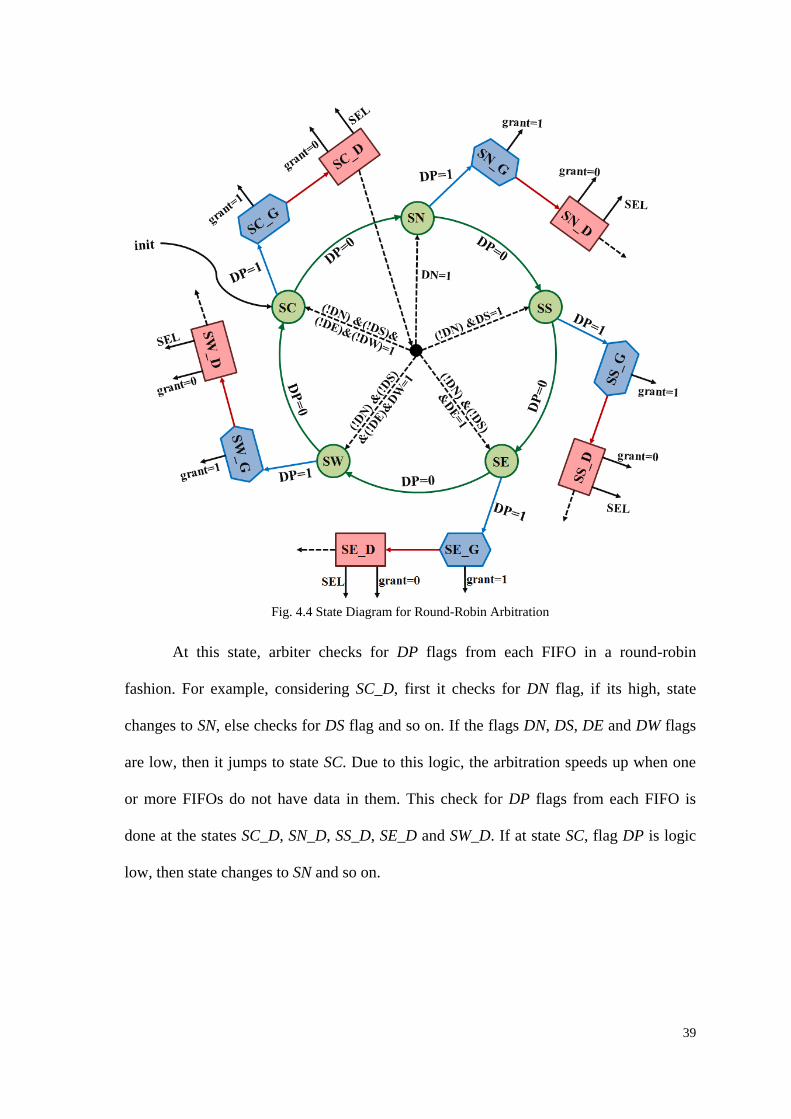
5.3 Arbiter module
In accordance with design of arbiter module explained in Section 4.3. The
waveforms obtained by the simulation can be observed in Fig. 5.2.
It can be inferred that cur_state changes cyclically through sc, sn, ss, se and sw at
every clock cycle. For simplicity purposes, without loss of generality, the subsequent
explanation would deal with „Core‟ set i.e. dpc, dest_c and grant_c. When cur_state is sc
and dpc is logic high, cur_state changes to sc_g and grant_c goes logic high. After a
clock cycle delay, cur_state changes to sc_d at which grant_c becomes logic low and sel
output is given based on dest_c.

47
Fig
. 5
.1 S
imu
lati
on
Wav
efo
rms
of
FIF
O B
uff
er m
od
ule
48
Fig
. 5
.2 S
imu
lati
on
Wav
efo
rms
of
Arb
iter
mo
du
le

49
5.4 Crossbar module
As per the described design in Section 4.4, the obtained simulation results are
displayed in Fig. 5.3.
The sample inputs have been chosen as 1111H, 2222H, 3333H, 4444H and
5555H for ci, ni, si, ei and wi respectively for ease in understanding the simulation
waveform. Depending on the sel lines, the outputs co, no, so, eo and wo obtain the
corresponding values of inputs as explained in Section 4.4.
5.5 Router module
The router module is obtained by the combination of the five FIFO Buffer
modules, arbiter module and crossbar module as elucidated in Fig. 4.1. The simulation
results for this module are shown in Fig. 5.4.
The minimum time required for a data packet to traverse through a Router is
given by the lowest latency as shown in Fig. 5.4 which is attained as 4 clock cycles.
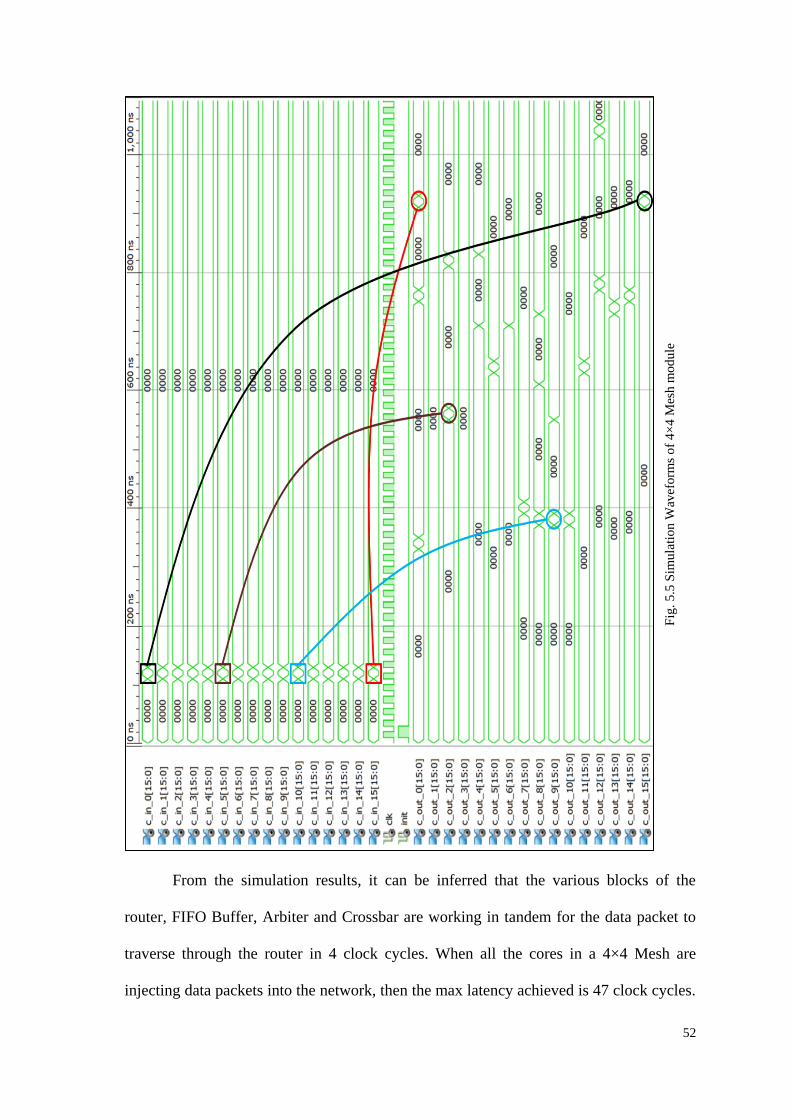
5.6 4×4 Mesh module
The 4×4 Mesh module is attained by combining sixteen routers in a way as
shown in Fig. 4.1. The obtained simulation results for this complete block are illustrated
in Fig. 5.5.
In the waveforms, four data packets have been marked to show their traversal
from source core to target core. The maximum time required for a data packet in the 4×4
Mesh would be when it traverses from Core „0‟ to Core „15‟ in Fig. 4.1. The latency for
this case has been found to be 47 clock cycles in simulation waveforms.

50
Fig
. 5
.3 S
imu
lati
on
Wav
efo
rms
of
Cro
ssb
ar m
od
ule

51
Fig
. 5
.4 S
imu
lati
on
Wav
efo
rms
of
Rou
ter
mod
ule
52
From the simulation results, it can be inferred that the various blocks of the
router, FIFO Buffer, Arbiter and Crossbar are working in tandem for the data packet to
traverse through the router in 4 clock cycles. When all the cores in a 4×4 Mesh are
injecting data packets into the network, then the max latency achieved is 47 clock cycles.
Fig
. 5
.5 S
imu
lati
on
Wav
efo
rms
of
4×
4 M
esh
mo
du
le

Chapter Six
Conclusion

54
The rapid scaling of devices led to the design of SoCs being communication-
centric and issued numerous challenges to researchers which gave rise to Network-on-
Chip technology. The field of NoC is beginning to have a tremendous influence in the
design of multicore and multilayer SoC architectures. In this dissertation, the various
concepts of NoC were analyzed mainly focusing in the area of NoC topology. Various
topologies were simulated in a network simulator NS2 and their performances assessed.
Through this dissertation, an attempt has been made to contribute to the field of NoC by
implementing a mesh topology which is a popular architecture for integration of regular-
sized cores.
In this project, a 4×4 Mesh topology for NoC has been designed in VHDL with
the help of Xilinx tools. Its implementation has been done in Virtex II Pro FPGA and the
functionality of the design has been verified. It can be concluded that the design perfectly
allows data packets to traverse through the network with a minimum latency of 4 clock
cycles per router length.
6.1 Scope of Future Work
The designed architecture of Mesh topology for NoC can be enhanced to improve
its latency and used for communication between some processing IP cores with the help
of Network Interface designs.

BIBLIOGRAPHY
[1] Arteris. A comparison of Network-on-Chip and Busses. [Online].
http://www.design-reuse.com/articles/10496/a-comparison-of-network-on-chip-
and-busses.html
[2] The International Technology Roadmap for Semiconductors, 2012 Update
Overview.
[3] L. Benini and G. D. Micheli, "Networks on Chips: A New SoC Paradigm,"
Computer, vol. 35, no. 1, pp. 70-78, Jan. 2002.
[4] K. Shuler, "The SoC Interconnect Fabric: A Brief History," Arteris, 2013.
[5] S. Young, et al., "A High I/O Reconfigurable Crossbar Switch," in Proceedings of
the 11th Annual IEEE Symposium on Field-Programmable Custom Computing
Machines, 2003.
[6] M. Ali, M. Welzl, A. Adnan, and F. Nadeem, "Using the NS-2 Network Simulator
for Evaluating Network on Chips (NoC)," in International Conference on
Emerging Technologies, 2006, pp. 506-512.
[7] J. Duato, S. Yalamanchili, and L. Ni, Interconnection Networks An Engineering
Approach. San Francisco, CA, USA: Morgan Kaufmann Publishers Inc., 2002.
[8] W. J. Dally and B. Towles, Principles and Practices of Interconnection Networks.
Elsevier Inc., 2004.
[9] A. V. d. Mello, L. C. Ost, F. G. Moraes, and N. L. V. Calazans, "Evaluation of
Routing Algorithms on Mesh Based NoCs," PUCRS, 2004.
[10] S. Kumar, et al., "A Network on Chip Architecture and Design Methodology," in
Proceedings of the IEEE Computer Society Annual Symposium on VLSI, 2002, pp.
105-112.
[11] J. Balfour and W. J. Dally, "Design tradeoffs for tiled CMP on-chip networks," in
Proc. of ACM Int’l Conf. on Supercomputing, 2006, pp. 187-198.

56
[12] W. J. Dally and B. Towles, "Route Packets, Not Wires: On-Chip Interconnection
Networks," in Proc. DAC, 2001, pp. 683-689.
[13] W. J. Dally and C. L. Seitz, "The torus routing chip," Journal of Distributed
Computing, pp. 187-196, 1986.
[14] Y. L. Jeang, W. H. Huang, and W. F. Fang, "A binary tree architecture for
application specific network on chip," in IEEE Asia-Pacific Conf. on Circuits and
Systems, 2004, pp. 877-880.
[15] P. Guerrier and A. Greiner, "A generic architecture for on-chip packet-switched
interconnections," in Proc. of DATE, 2000, pp. 250-256.
[16] P. P. Pande, C. Grecu, A. Ivanov, and R. Saleh, "High-throughput switch-based
interconnect for future SoCs," in Proc. of IEEE Int’l Workshop on System-on-Chip
for Real Time Applications, 2003, pp. 304-310.
[17] P. P. Pande, C. Grecu, M. Jones, S. M. Andre Ivanov, and R. Saleh, "Performance
Evaluation and Design Trade-Offs for Network-on-Chip Interconnect
Architectures," IEEE Transactions on Computers, vol. 54, no. 8, pp. 1025-1040,
Aug. 2005.
[18] A. Hemani, et al., "Network on a Chip: An architecture for billion transistor era," in
Proceedings of the IEEE NorChip Conference, Nov. 2000.
[19] V.-D. Ngo and H.-W. Choi, "On chip network: topology design and evaluation
using NS2," in Proceedings of Advanced Communication Technology, 2005.
[20] T. F. Pereira and C. A. Zeferino. A Set of VHDL IPs to Evaluate Performance of
Netwoks-on-Chip. [Online]. http://www.design-reuse.com/articles/21817/noc-
performance-evaluation.html
[21] A. Shrivastava and A. K. Pandit, "Design and Performance Evaluation of a NOC-
Based Router Architecture for MPSoC," in Fourth International Conference on
Computational Intelligence and Communication Networks, 2012.

57
[22] D. Wang, C. Lo, J. Vasiljevic, N. E. Jerger, and J. G. Steffan, "DART: A
Programmable Architecture for NoC Simulation on FPGAs," IEEE Transactions
on Computers, vol. 63, no. 3, pp. 664-678, Mar. 2014.
[23] The Network Simulator - ns-2. [Online]. http://www.isi.edu/nsnam/ns/
[24] T. Issariyakul and E. Hossain, Introduction to Network Simulator NS2. Springer,
2009.
[25] M. Stutz, Get started with GAWK: AWK language fundamentals. developerWorks,
2006.
[26] S. Swapna, A. K. Swain, and K. K. Mahapatra, "Design and Analysis of five port
router for Network on Chip," in Asia-Pacific Conference on Postgraduate
Research in Microelectronics & Electronics, December 2012.
[27] J. Y. Chang and H. J. Cho, "Crossbar switch architecture for multi-processor SoC
platform," USA Patent US7554355 B2, Jun. 30, 2009.
[28] W.-C. Tsai, Y.-C. Lan, Y.-H. Hu, and S.-J. Chen, "Networks on Chips: Structure
and DesignMethodologies," Journal of Electrical and Computer Engineering, vol.
2012.
[29] S. Kundu, J. Soumya, and S. Chattopadhyay, "Design and evaluation of Mesh-of-
Tree based Network-on-Chip using virtual channel router," Microprocessors and
Microsystems, vol. 36, pp. 471-488, Jun. 2012.
[30] D. o. E. a. C. Engineering, "SystemC based NoC (Network-on-Chip) Modeling
Course Project," Ryerson University.
[31] Y.-R. Sun, "Simulation and Performance Evaluation for Networks on Chip," M. S.
thesis, KTH Royal Institute of Technology, December 2001.
[32] S. A. B. M. Junos, "Network-On-Chip Mesh Topology Modeling and Performance
Analysis," M. E. thesis, Universiti Teknologi Malaysia, May 2009.

PUBLICATIONS
[1] T. Neel Kamal Reddy, Ayas Kanta Swain, Jayant K. Singh and K. K. Mahapatra,
“Performance Assessment of Different Network-on-Chip Topologies,” International
Conference on Devices, Circuits and Systems, Mar-2014.
[2] Jayant K. Singh, Ayas Kanta Swain, T. Neel Kamal Reddy and K. K. Mahapatra,
“Performance evaluation of different routing algorithms in Network on Chip,” IEEE
Asia Pacific Conference, pp. 180-185, December 2013.


![Topology-Adaptive Mesh Deformation for Surface Evolution, … · Topology-Adaptive Mesh Deformation for Surface Evolution, Morphing, and Multi-View Reconstruction. [Research Report]](https://img.dokumen.tips/doc/110x75/5f785df833d37a1d7d2d6044/topology-adaptive-mesh-deformation-for-surface-evolution-topology-adaptive-mesh.jpg)