Embed Size (px)
Citation preview

VLSI DESIGN (III Year II Semester-ECE)
COURSE OBJECTIVES AND OUTCOMES
The objectives the course are to:
Give exposure to different steps involved in the fabrication of ICs using MOS transistor,
CMOS/BiCMOS transistors and passive components.
Explain electrical properties of MOS and BiCMOS devices to analyze the behaviour of
inverters designed with various loads.
Give exposure to the design rules to be followed to draw the layout of any logic circuit.
Provide concept to design different types of logic gates using CMOS inverter and analyze
their transfer characteristics.
Provide design concepts to design building blocks of data path of any system using gates.
Understand basic programmable logic devices and testing of CMOS circuits.
The outcomes of the course are to:
Upon successfully completing the course, the student should be able to
Acquire qualitative knowledge about the fabrication process of integrated circuit using MOS
transistors.
Choose an appropriate inverter depending on specifications required for a circuit.
Draw the layout of any logic circuit which helps to understand and estimate parasitics of any
logic circuit.
Design different types of logic gates using CMOS inverter and analyze their transfer
characteristics.
Provide design concepts required to design building blocks of data path using gates.
Design simple memories using MOS transistors and can understand design of large memories.
Design simple logic circuit using PLA, PAL, FPGA and CPLD.

Understand different types of faults that can occur in a system and learn the concept of testing
and adding extra hardware to implement testability of system.
SYLLABUS
UNIT I: INTRODUCTION & BASIC ELECTRICAL PROPERTIES.

Introduction to IC Technology – MOS, PMOS, NMOS, CMOS & BiCMOS technologies. Basic
Electrical Properties of MOS and BiCMOS Circuits: Ids-Vds relationships, MOS transistor threshold
Voltage, gm, gds, figure of merit, Pass transistor, NMOS Inverter, Various pull ups, CMOS Inverter
analysis and design, Bi-CMOS Inverters.
UNIT II: VLSI CIRCUIT DESIGN PROCESSES.
VLSI Design Flow, MOS Layers, Stick Diagrams, Design Rules and Layout, 2 µm CMOS Design
rules for wires, Contacts and Transistors Layout Diagrams for NMOS and CMOS Inverters and Gates,
Scaling of MOS circuits.
UNIT III : GATE LEVEL DESIGN.
Logic Gates and Other complex gates, Switch logic, Alternate gate circuits, Time Delays, Driving
large Capacitive Loads, Wiring Capacitances, Fan-in and fan-out, Choice of layers.
UNIT IV: DATA PATH SUBSYSTEMS & ARRAY SUBSYSTEMS
Subsystem Design, Shifters, Adders, ALUs, Multipliers, Parity generators, Comparators, Zero/One
Detectors, Counters, SRAM, DRAM, ROM, Serial access memories.
UNIT V: PROGRAMMABLE LOGIC DEVICES AND CMOS TESTING.
PLAs, FPGAs, CPLDs, Standard Cells, Programmable Array Logic, Design Approach, Parameter
influencing low power design, CMOS Testing, Need for testing, Test Principles, Design Strategies for
test, Chip-level Test Techniques.
TEXTBOOKS :
1. Essentials of VLSI circuits and systems – Kamran Eshraghian, Eshraghian Dougles and A.
Pucknell, PHI, 2005 Edition.
2. CMOS VLSI Design- a Circuits and systems Perspective – Neil Weste, David Harri, Ayan
Banerjee, 3rd Ed, Pearson, 2009.
3. VLSI Design-M. Michael Vai, 2001. CRC Press.
REFERENCES :
1. Introduction to VLSI Systems: A logic circuit and Systems Perspectives-Ming-BO Lin, CRC Press-
2011.
2. CMOS logic circuit Design- John P. Uyemura, Springer, 2007.
3. Modern VLSI Design - Wayne Wolf, Pearson Education, 3rd Edition, 1997. 4. VLSI Design – K. Lal Kishore, V. S. V. Prabhakar, I. K. International, 2009. 5. Introduction to VLSI – Mead & Convey, BS Publications, 2010.
UNIT-I INTRODUCTION & BASIC ELECTRICAL PROPERTIES
OBJECTIVE TYPE QUESTIONS
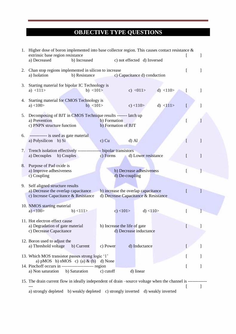
1. Higher dose of boron implemented into base collector region. This causes contact resistance &
extrinsic base region resistance [ ] a) Decreased b) Increased c) not effected d) Inversed
2. Chan stop regions implemented in silicon to increase [ ] a) Isolation b) Resistance c) Capacitance d) conduction
3. Starting material for bipolar IC Technology is a) <111> b) <101> c) <011> d) <110> [ ]
4. Starting material for CMOS Technology is
a) <100> b) <101> c) <110> d) <111> [ ]
5. Decomposing of BJT in CMOS Technique results ------- latch up
a) Prevention b) Formation [ ] c) PNPN structure function b) Formation of BJT
6. ------------ is used as gate material
a) Polysilicon b) Si c) Cu d) Al [ ]
7. Trench isolation effectively ---------------- bipolar transistors
a) Decouples b) Couples c) Forms d) Lower resistance [ ]
8. Purpose of Pad oxide is
a) Improve adhesiveness b) Decrease adhesiveness [ ] c) Coupling d) De-coupling
9. Self aligned structure results
a) Decrease the overlap capacitance b) increase the overlap capacitance [ ] c) Increase Capacitance & Resistance d) Decrease Capacitance & Resistance
10. NMOS starting material a) <100> b) <111> c) <101> d) <110> [ ]
11. Hot electron effect cause a) Degradation of gate material b) Increase the life of gate [ ]
c) Decrease Capacitance d) Decrease inductance
12. Boron used to adjust the a) Threshold voltage b) Current c) Power d) Inductance [ ]
13. Which MOS transistor passes strong logic ‘1’ [ ] a) pMOS b) nMOS c) (a) & (b) d) None
14. Pinchoff occurs in ---------------------- region [ ]
a) Non saturation b) Saturation c) cutoff d) linear
15. The drain current flow in ideally independent of drain –source voltage when the channel is -------------
--- [ ]
a) strongly depleted b) weakly depleted c) strongly inverted d) weakly inverted

16. ------------------------- process is used to transfer the layout pattern from masks to wafer. [ ]
a) Diffusion b) Isolation c) photolithographic d) metallization
17. According to Moore’s law, the number of transistors that could be manufactured on a chip [ ] a) linearly decreases b) grows exponentially c) grows linearly d) decreases exponentially
18. The transistor threshold voltage, VT is ----------------------- for P type transistor. a) positive b) negative c) zero d) Infinity [ ]
19. The present feature size of a transistor is ----------------- [ ]
a) 0.5 m b) 0.13 m c) 0.75 m d) 1 m
20. Pick out the advantage of IC [ ]
a) Smaller physical size b) Low power consumption c) Reduced cost d) All
21. In the MOSFET, as width of channel increases Id [ ] a) Increases b) decreases c) Constant d) none
22. Latch – up is caused by [ ]
a) Parasitic R b) Parasitic BJT’s c) (a) & (b) d) Parasitic C
23. Pick up latch-up resistant CMOS process [ ]
a) n well b) p well c) silicon on Insulator d) all
24. Cascaded inverters are used to drive large _____________ loads [ ]
a) Capacitive b) resistive c) inductive d) all
25. In which process (CMOS) pFETs are embedded in n well [ ]
a) p well b) n well c) SOI d) all
26. In the Pseudo-nMOS logic ----------- transistor is used as pull-up resistor [ ]
a)pMOS b) nMOS c) Bipolar d) Unijunction
27. Latch structure is used in ------------ Logic [ ]
a)Pseudo-nMOS b) DCVS c) Domino d) all
28. Routing channel is spacing between [ ]
a)cell rows b) cells c) wires d) None
29. Feed throughs are used during [ ]
a)Placement b) Routing c) Floor planning d) Synthesis
30. For n-type transistor threshold voltage is ______________ [ ]
a) Positive b) negative c) zero d) none
31. In the twin tub process ____________ wafer is used [ ]
a) p-doped b) n-doped c) undoped d) none

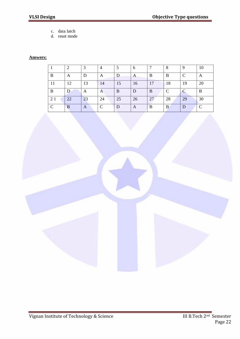
Answers:
1 2 3 4 5 6 7 8 9 10
B A D A D A B B C A
11 12 13 14 15 16 17 18 19 20
A A B B A C B B B D
21 22 23 24 25 26 27 28 29 30
B B A A B A B C C A
31
C
UNIT-II VLSI CIRCUIT DESIGN PROCESSES

OBJECTIVE TYPE QUESTIONS
1.The smallest feature size of a transistor is [ ]
a) 4 x 4 b) 2 x 2 c) 8 x 8 d) 1 x 1
2.The on resistance of pulling transistor in an nmos inverter is [ ]
a) 10K b) 50K c) 40K d) 20K
3.The inverter pair delay for inverter having 4:1 ratio is [ ]
a) 4 b) 1 c) 2 d) 5
4.The rise time to fall time ratio is given by ----------------------
a) p
n
f
r
b) pn
f
r
c) 1
f
r
d) none
5.Metal to metal contact is called --------------- [ ]
a) Buried contact b) Butting contact c) Via d) contact out
6.The capacitance that is caused by the edges of conductor is --------------- capacitance.
a) Fringing field capacitance b) Diffusion capacitance [ ]
c) Gate to channel capacitance d) Area capacitance.
7.Measure of quality of logic circuit family is [ ]
a) Speed power product b) Voltage c) Days d) Current
8.Elmore delay model E =
a)
0
)( dtttVOut b)
0
)( dttVOut c)
0
tdt d)
dttVOut [ ]
9.------------------ model is used to compute delay [ ]
a) RC Transmission line b) R model c) L model d) C model
10.The following is one of the method for CMOS Technology
a) Twin tub b) Three tub c) Four tub d) Five tub [ ]
11.In Bi-polar Technology ----------- is used to get small diffusion coeffecient
a) Antimony b) Phosphorous c) Gold d) Copper [ ]
12.Base Collector capacitance can be minimized is n epitaxial layer is
a) Lightly doped b) Heavily doped c) Moderate d) no doping [ ]
13.Burried layer sheet resistance is
a) 5 to 15 / Sq b) 1 to 3 / Sq c) 1 to 5/Sq d) none [ ]
14.---------------- is used as Passivation layer [ ]
a) Si3N4 b) Si c) Si N d) Si2O2
15. In CMOS inverter to have equal raise & fall times , Wp is approximately equal to
a) (23) Wn b) Wn c) (34) Wn d) Wn/2 [ ]
16. Power Consumption of CMOS circuits depends on [ ] a) Switching frequency b) load capacitance c) Supply voltages d) all
17. Quality of logic circuit family is [ ]

a) Delay X power dissipation b) delay / power dissipation c) power dissipation / delay d) Delay + power dissipation.
18. Cascaded inverters are used to drive large _____________ loads [ ]
a) Capacitive b) resistive c) inductive d) all
19. In which process (CMOS) pFETs are embedded in n well [ ]
a) p well b) n well c) SOI d) all 20. Latch – up is caused by [ ]
a) Parasitic R b) Parasitic BJT’s c) (a) & (b) d) Parasitic C
Answers:
1 2 3 4 5 6 7 8 9 10
B B C B C C B C C A
11 12 13 14 15 16 17 18 19 20
D C A A D A D B C B
UNIT-III GATE LEVEL DESIGN

OBJECTIVE TYPE QUESTIONS
1. Electromigration of metal leads to _____ circuit. [ ]
a) Open b) short c) Amplifier d) Rectifier
2. Design rules are geometrical constraints on [ ]
a) stick diagram b) Layout c) circuit d) program
3. Circuit extractor extracts [ ]
a) Component b) wire c) (a) & (b) d) Nothing
4. In which gates operation is independent of stored charge [ ]
a) Dynamic b) static c) Complementary d) all
5. If pullup network consist of series connected nFETs, the gate is [ ]
a) NAND b) NOR c) NOT d) None
6. Dual of parallel connection is [ ]
a) Parallel b) Series c) Series-parallel d) none
7. In CMOS inverter to have equal raise & fall times , Wp is approximately equal to
a) (23) Wn b) Wn c) (34) Wn d) Wn/2 [ ]
8. Power Consumption of CMOS circuits depends on [ ]
a) Switching frequency b) load capacitance c) Supply voltages d) all
9. Quality of logic circuit family is [ ]
a) Delay X power dissipation b) delay / power dissipation
c) power dissipation / delay d) Delay + power dissipation.
10. The control inputs in BILBO testing the coresponding mode is [ ]
a. linear shift mode
b. signature analysis mode
c. datalatch d. reset mode
11. In the BILBO arrangements, when C0=0, C1=1 then the corresponding mode is [ ]
a. linear shift mode
b. signature analysis mode
c. data latch
d. reset mode
12. The following the mode when C0=1, and C1=0 in the BILBO arrangement [ ]
a. linear shift mode b. signature analysis mode
c. data latch
d. reset mode
13. On chip testing is obtained by using [ ]
a. self - test circuitry
b. adhoc testability

c. structured testability d. LSSD approach
14. Signature analysis techniques are [ ]
a. on chip testing
b. structured testing
c. LSSD testing
d. adhoc testability
15. The manufacturing cost is low by detecting the malfunctioning of chip at a level of[ ]
a. wafer level b. packaged-chip
c. system level
d. field
16. The tests that are usually carried after chip is manufactured are called [ ]
a. functionality test b. design verification
c. manufacturing test
d. technology test
17. Generally memories are tested by [ ]
a. self-test
b. full serial scan c. parallel scan
d. LFSR method
18. In order to reconfogure flip - flops appropriately, it is necessary to be able to include a double throw switch in the [ ]
a. simple scan path
b. address path c. control singnal path
d. data path
19. The test access port or TAP controller in a boundry - scan system level testing is a[ ]
a. 16 - state FSM
b. 8 - state register c. 8 - state interface pins
d. 16 - state NAND gates
20. For a CMOS gate which is the best speed power product?
a. 1.4pJ
b. 1.6pJ
c. 3.4pJ
d. 4.4pJ
ANSWERS:
1 2 3 4 5 6 7 8 9 10
B B A D B D B C B
11 121 13 14 15 16 17 18 19 20
A D B A A A C A D B

VLSI Design Objective Type questions
Vignan Institute of Technology & Science III B.Tech 2nd Semester Page 14
UNIT-IV DATA PATH SUBSYSTEMS & ARRAY SUBSYSTEMS

VLSI Design Objective Type questions
Vignan Institute of Technology & Science III B.Tech 2nd Semester Page 15
OBJECTIVE TYPE QUESTIONS
1. The carry chain in adder is consist with [ ]
a. cross-bar swith b. transmission gate
c. bus interconncection
d. pass transistors 2. VLSI design of adder element basically requires [ ]
a. EX-OR gate, Not and OR gates
b. multiplexers, inverter circuit and communication paths c. multiplexers, EX-OR and NAND gates
d. inverter circuits and communication paths 3. Carry line in adder must be buffered after or before each adder element because [ ]
a. slow response of series pass transistors
b. slow response of parallel line
c. fast response of parallel pass transistors d. fast response of series line
4. The ALU logical functions can be obtained by a suitable switching of the [ ]
a. carry line between adder elements b. sum line between adder elements
c. carry line between shifter & buffer
d. sum line between shifter & buffer 5. To fast an arithmetic operations, the multipliers and dividers is to use architecture of[ ]
a. parallel b.serial c. pipelined d.switched 6. The number of bits increases in comparator then the [ ]
a. height increases c. width reduces linearly
b. width grows linearly d.height reduces
7. The standard cell for an n-bit parity generator is [ ]
a. n-1 bit cell c. two bit cell b. one bit cell d.n+1 bit cell
8. The parity information is passed from one cell to the next and is modified or not by a cell depending on the state of the [ ]
a. previous information c. input lines
b. output line d.next information
9. The parity information (pi) passed from one cell to the next is modified when the input line (Ai) is at the state of [ ]
a. zero b.overline{A}i c.one d.independent of input line state 10. For the 4X4 bit barrel shifter, the regularity factor is given by [ ]
a. 8 b.4 c.2 d.16 11. The level of any particular design can be measured by [ ]
a. SNR c.Ratio of amplitudes
b. regularity d.quality 12. In tackling the design of system the more significant property is [ ]

VLSI Design Objective Type questions
Vignan Institute of Technology & Science III B.Tech 2nd Semester Page 16
a. logical operations b. topological properties b. test ability d.nature of architecture
13. Any bit shifted out at one end of data word will be shifted in at the other end of the word is called [ ]
a. end-around b.end-off c.end-less d.end-on 14. In the VLSI design the data and control signals of a shift register flow in [ ]
a. horizontally and vertically b. vertically and horizontally
c. both horizontally
d. both vertically 15. The subsystem design is classified as [ ]
a. first level c. bottom level
b. top level d.leaf-cell level 16. The larger system design must be partition into a sub systems design such that [ ]
a. minimum interdependence and inter connection b. complexity of interconnection
c. maximum interdependence
d. arbitarily chosen 17. To simplify the subsystem design, we generally used the [ ]
a. interdependence c. regular structures
b. complex interconnections d.standard cells 18. System design is generally in the manner of [ ]
a. down-top b.top-down c.bottom level only d.top level only 19. Structured design begins with the concept of [ ]
a. hierarchy
b. down-top design
c. bottom level design d. complex function design
20. Any general purpose n-bit shifter should be able to shift incoming data by up to number of places are [ ]
a. n b.2n c.n-1 d.2n-1 21. For a four bit word, a one-bit shift right is equivalent to a [ ]
a. two bit shift left c. one bit shift left
b. three-bit shift left d.four-bit shift left 22. The type of switch used in shifters is [ ]
a. line switch c. crossbar switch
b. transistor type switch d.gate switch
Answers:
1 2 3 4 5 6 7
D B A A C B B
8 9 10 11 12 13 14
C C D D C A A
VLSI Design Objective Type questions
Vignan Institute of Technology & Science III B.Tech 2nd Semester Page 17
15 16 17 18 19 20 21
D A D B C B C
22
D

VLSI Design Objective Type questions
Vignan Institute of Technology & Science III B.Tech 2nd Semester Page 18
UNIT-V PROGRAMMABLE LOGIC DEVICES & CMOS TESTING
VLSI Design Objective Type questions
Vignan Institute of Technology & Science III B.Tech 2nd Semester Page 19
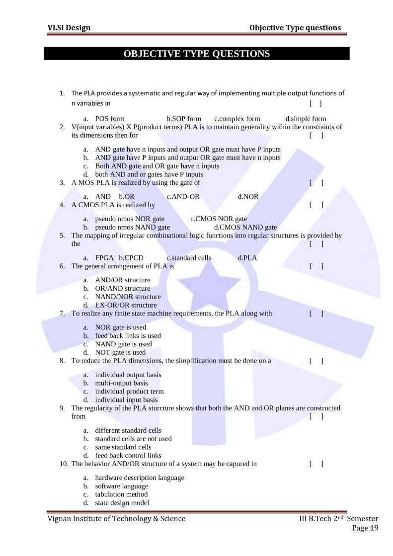
OBJECTIVE TYPE QUESTIONS
1. The PLA provides a systematic and regular way of implementing multiple output functions of
n variables in [ ]
a. POS form b.SOP form c.complex form d.simple form 2. V(input variables) X P(product terms) PLA is to maintain generality within the constraints of
its dimensions then for [ ]
a. AND gate have n inputs and output OR gate must have P inputs b. AND gate have P inputs and output OR gate must have n inputs
c. Both AND gate and OR gate have n inputs
d. both AND and or gates have P inputs 3. A MOS PLA is realized by using the gate of [ ]
a. AND b.OR c.AND-OR d.NOR 4. A CMOS PLA is realized by [ ]
a. pseudo nmos NOR gate c.CMOS NOR gate
b. pseudo nmos NAND gate d.CMOS NAND gate 5. The mapping of irregular combinational logic functions into regular structures is provided by
the [ ]
a. FPGA b.CPCD c.standard cells d.PLA 6. The general arrangement of PLA is [ ]
a. AND/OR structure
b. OR/AND structure c. NAND/NOR structure
d. EX-OR/OR structure 7. To realize any finite state machine requirements, the PLA along with [ ]
a. NOR gate is used
b. feed back links is used
c. NAND gate is used d. NOT gate is used
8. To reduce the PLA dimensions, the simplification must be done on a [ ]
a. individual output basis b. multi-output basis
c. individual product term
d. individual input basis 9. The regularity of the PLA sturcture shows that both the AND and OR planes are constructed
from [ ]
a. different standard cells b. standard cells are not used
c. same standard cells
d. feed back control links 10. The behavior AND/OR structure of a system may be capured in [ ]
a. hardware description language
b. software language c. tabulation method
d. state design model

VLSI Design Objective Type questions
Vignan Institute of Technology & Science III B.Tech 2nd Semester Page 20
11. VHDL differs from other software languages by including [ ]
a. behaviour of system
b. compilers, debuggers and simulatois
c. syntax d. machine understanding language
12. The advantage of fuse-based FPGAS compared to other FPGAs is [ ]
a. allows large number of interconnections b. complex fabrication process
c. larger in size
d. modified without changing hardware 13. Where the design is of moderate complexity and time to silicon is of paramount importance
then the probably suitable approach is [ ]
a. FPGA b.PLA c.standard cell d.PAL 14. A single time programmable FPGA is the type of [ ]
a. fuse-based FPGA b. SRAM-FPGA
c. EPROM-FPGA
d. Flash based FPGA 15. The SRAM-FPGA's consists of a large array of programmable logic cells known as[ ]
a. Erasable programmable logic devices-EPLD
b. configurable logic blocks-CLB c. micro cells
d. AND/OR array 16. The fabrication process of EPROM-FPGA is [ ]
a. easy and high integration density
b. easy and low integration density
c. complex and high integration density d. complex and low integration density
17. The following is a chip whose final logic sturcture is directly configured by the end user [ ]
a. gate array design b. field programmable logic
c. standard cell design
d. full custom design 18. FPGA can be programmed as per the [ ]
a. positive logic
b. negative logic c. users logic
d. fixed logic 19. The logic cells in FPGA contains [ ]
a. only combinational circuits
b. only sequential circuits
c. both combinational & sequential circuits d. only Flip-Flop circuits
20. The individual cells of FPGA are interconnected by [ ]
a. AND gates and switches b. matrix of wires and programmable switches
c. OR gates and non programmable switches
d. AND & OR gates

VLSI Design Objective Type questions
Vignan Institute of Technology & Science III B.Tech 2nd Semester Page 21
21. Generally the system is partitioned for testing because [ ] a. reducing the chip area
b. reducing the no. of pads
c. reducing the number of test vectors
d. reduce the required power 22. The two key concepts underlying all considerations for testabiloity are [ ]
a. set and reset b. controllability and observability
c. intial and final conditions
d. pads and links 23. Controllability in testing means [ ]
a. being able to set known internal states
b. being able to generate all states c. being able to generate all combinations of circuit states
d. read out the result of the state changes 24. Being able to generate all states to fully excise all combinations of circuit states is called [ ]
a. controllability
b. observability
c. combinationatorial testbility d. reset facility
25. Being able to read out the result of the state changes as they occur is called [ ]
a. controllability b. reset facility
c. combinational testability
d. observality 26. The facults occure due to thin-oxide shorts or metal-to metal shorts are called [ ]
a. stuck at zero facults
b. short-circuit faults c. open-circuit faults
d. bridge faults 27. Radom logic is probably best tested via [ ]
a. self testing
b. full serial scan or parallel scan
c. boundary scan d. LFSR method
28. Self-test circuitry approach is based on [ ]
a. linear feed back shift registers only b. linear feed back shift registers, exclusive-OR and clock system or gate
c. clock system only
d. enclusive OR gates only 29. The combination of LSSD scan path and linear feed back shift register is called [ ]
a. self test circuitry
b. signature analysis technique c. structured testbility
d. built-in logic block observation
30. In the following which one is corrcet with respect to BILBO testing for control inputs C0=1, C1=1 [ ]
a. linear shift mode
b. signature analysis mode
VLSI Design Objective Type questions
Vignan Institute of Technology & Science III B.Tech 2nd Semester Page 22
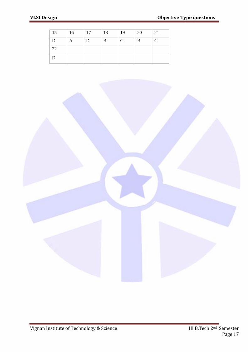
c. data latch d. reset mode
Answers:
1 2 3 4 5 6 7 8 9 10
B A D A D A B B C A
11 12 13 14 15 16 17 18 19 20
B D A A B D B C C B
2 1 22 23 24 25 26 27 28 29 30
C B A C D A B B D C

MODEL QUESTION PAPER
ELECTRONICS AND COMMUNICATION ENGINEERING
VLSI SYSTEM DESIGN
PART-A
1. What are the different mos layers? [2M]
2. What are the two types of design rules? [2M]
3. Define rise time and fall time? [2M]
4. Draw the boundary scan input logic diagram? [2M]
5. Define threshold voltage? [2M]
6. Discuss the steps involved in IC fabrication process? [3M]
7. Draw the pseudo nmos inverter circuit diagram? [3M]
8. What are scan based test techniques? [3M]
9. What is channel length modulation and body effect? [3M]
10. Draw the cmos inverter circuit diagram? [3M]
PART-B
11. a) Derive the relation between IDS & VDS of MOSFET. [16 M].
OR
b) Draw the circuit for NMOS inverter and explain its operation. [16 M].
12. a) Design a stick diagram for CMOS logic shown below. [16 M]
i. Y = (A + B).C
ii. Y = (A B)+C
OR
b) Implement the following logic functions using nMOS logic. [16 M]
i. Y = {AB + CD}
ii. Y = {A.B.C + D}
1. a). Calculate the pair delay Vin to Vout in terms of τ for the given data. [16 M]
Inverter -A
Lpu= 16λ , WP.U = 2 λ , Lpd = 2 λ , Wpd = 2 λ

Inverter -B
Lpu= 2λ , WP.U = 2 λ , Lpd = 2 λ , Wpd = 8 λ
OR
b). Calculate the gate capacitance value of 1.2μm Technology minimum sized transistor
with gate to cannel capacitance value is 16 × 10−4pF/μm2 [16 M].
15. a). Explain the principle of a DRAM cell using neat diagram. [16 M].
OR
b). Give the schematic of a DRAM and explain how READ and WRITE operations are
carried out. [16 M].
16. a). Explain about the principle and operation of FPGAs. What are its applications? [16 M].
OR
b). Give the Architecture of a boundary scan test and explain the same. [16 M].
****THE END***


![vlsi & embedded systems lab - SIETK ECE DEPARTMENT · 2018. 7. 16. · SIETK, ECE [VLSI & EMBEDDED SYSTEMS LAB] 2 (15A04712) VLSI & EMBEDDED SYSTEMS LABORATORY Note: The students](https://img.dokumen.tips/doc/110x75/60a68df82b16b22c09239fcb/vlsi-embedded-systems-lab-sietk-ece-department-2018-7-16-sietk-ece.jpg)


![Ece-V-fundamentals of Cmos Vlsi [10ec56]-Solution](https://img.dokumen.tips/doc/110x75/55cf9d28550346d033ac77f4/ece-v-fundamentals-of-cmos-vlsi-10ec56-solution.jpg)