Embed Size (px)
Citation preview
1
Unit 1 1Y.-W. Chang
VLSI Design Automation張耀文
Yao-Wen [email protected]
http://cc.ee.ntu.edu.tw/~ywchangGraduate Institute of Electronics Engineering
Department of Electrical EngineeringNational Taiwan University
Taipei 106, TaiwanSpring 2004
943/U0220 & #901/60010
Unit 1 2Y.-W. Chang
Administrative Matters˙Time/Location: Thursdays 9:10am--12:10pm; EE#2-144.˙Instructor: Yao-Wen Chang.˙E-mail: [email protected]˙URL: http://cc.ee.ntu.edu.tw/~ywchang.˙Office: EE#2-548. (Tel) 2363-5251x 548; (Fax) 2364-1972.˙Office Hours: Thursdays 2-3pm˙Teaching Assistants
陳泰蓁 Tai-Chen Chen ([email protected]) 陳東傑 Tung-Chieh Chen ([email protected])
˙Prerequisites: data structures (or discrete math) & logic design.
˙Required Text: S. H. Gerez, Algorithms for VLSI Design Automation, John Wiley & Sons, 1999
˙References: supplementary reading materials will be provided.
2
Unit 1 3Y.-W. Chang
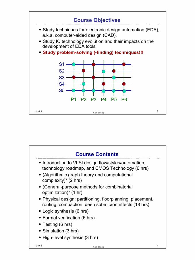
Course Objectives˙Study techniques for electronic design automation (EDA),
a.k.a. computer-aided design (CAD).˙Study IC technology evolution and their impacts on the
development of EDA tools˙Study problem-solving (-finding) techniques!!!
S1S2S3S4S5
P1 P2 P3 P4 P5 P6
Unit 1 4Y.-W. Chang
Course Contents˙Introduction to VLSI design flow/styles/automation,
technology roadmap, and CMOS Technology (6 hrs)˙(Algorithmic graph theory and computational
complexity)* (2 hrs) ˙(General-purpose methods for combinatorial
optimization)* (1 hr)˙Physical design: partitioning, floorplanning, placement,
routing, compaction, deep submicron effects (18 hrs)˙Logic synthesis (6 hrs)˙Formal verification (6 hrs)˙Testing (6 hrs)˙Simulation (3 hrs)˙High-level synthesis (3 hrs)
3
Unit 1 5Y.-W. Chang
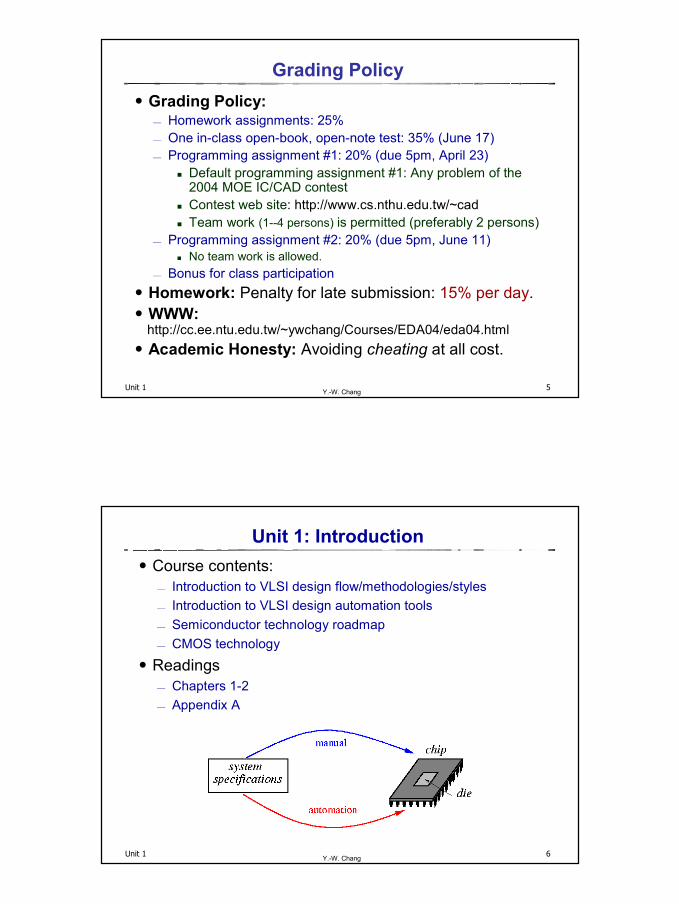
Grading Policy˙Grading Policy:
Homework assignments: 25% One in-class open-book, open-note test: 35% (June 17) Programming assignment #1: 20% (due 5pm, April 23)
Default programming assignment #1: Any problem of the 2004 MOE IC/CAD contestContest web site: http://www.cs.nthu.edu.tw/~cadTeam work (1--4 persons) is permitted (preferably 2 persons)
Programming assignment #2: 20% (due 5pm, June 11)No team work is allowed.
Bonus for class participation˙Homework: Penalty for late submission: 15% per day. ˙WWW:
http://cc.ee.ntu.edu.tw/~ywchang/Courses/EDA04/eda04.html˙Academic Honesty: Avoiding cheating at all cost.
Unit 1 6Y.-W. Chang
Unit 1: Introduction˙Course contents:
Introduction to VLSI design flow/methodologies/styles Introduction to VLSI design automation tools Semiconductor technology roadmap CMOS technology
˙Readings Chapters 1-2 Appendix A
4
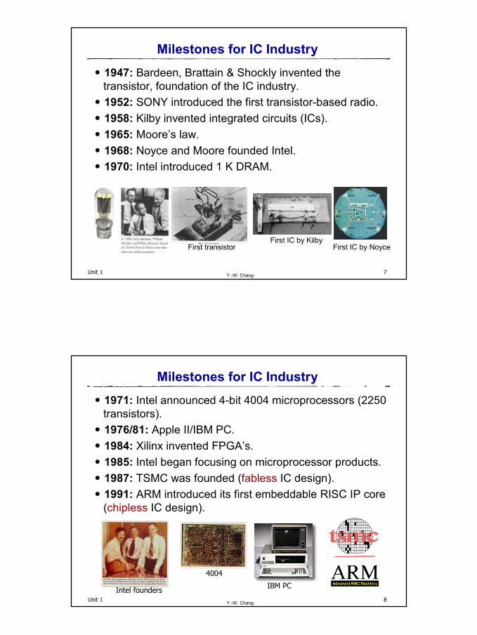
Unit 1 7Y.-W. Chang
Milestones for IC Industry˙1947: Bardeen, Brattain & Shockly invented the
transistor, foundation of the IC industry.˙1952: SONY introduced the first transistor-based radio.˙1958: Kilby invented integrated circuits (ICs).˙1965: Moore’s law.˙1968: Noyce and Moore founded Intel.˙1970: Intel introduced 1 K DRAM.
First transistor First IC by NoyceFirst IC by Kilby
Unit 1 8Y.-W. Chang
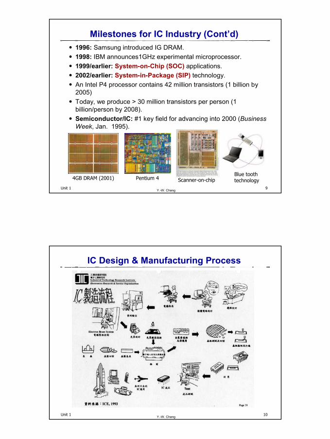
Milestones for IC Industry˙1971: Intel announced 4-bit 4004 microprocessors (2250
transistors).˙1976/81: Apple II/IBM PC.˙1984: Xilinx invented FPGA’s.˙1985: Intel began focusing on microprocessor products.˙1987: TSMC was founded (fabless IC design).˙1991: ARM introduced its first embeddable RISC IP core
(chipless IC design).
4004
Intel founders IBM PC
5
Unit 1 9Y.-W. Chang
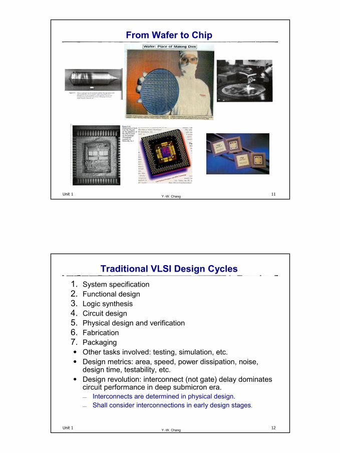
Milestones for IC Industry (Cont’d)˙1996: Samsung introduced IG DRAM.˙1998: IBM announces1GHz experimental microprocessor. ˙1999/earlier: System-on-Chip (SOC) applications.˙2002/earlier: System-in-Package (SIP) technology.˙An Intel P4 processor contains 42 million transistors (1 billion by
2005)˙Today, we produce > 30 million transistors per person (1
billion/person by 2008).˙Semiconductor/IC: #1 key field for advancing into 2000 (Business
Week, Jan. 1995).
Pentium 4 Scanner-on-chip4GB DRAM (2001)Blue tooth technology
Unit 1 10Y.-W. Chang
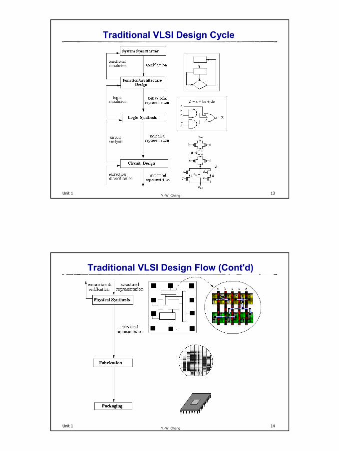
IC Design & Manufacturing Process
6
Unit 1 11Y.-W. Chang
From Wafer to Chip
Unit 1 12Y.-W. Chang
Traditional VLSI Design Cycles1. System specification2. Functional design3. Logic synthesis4. Circuit design5. Physical design and verification6. Fabrication 7. Packaging ˙ Other tasks involved: testing, simulation, etc.˙ Design metrics: area, speed, power dissipation, noise,
design time, testability, etc.˙ Design revolution: interconnect (not gate) delay dominates
circuit performance in deep submicron era. Interconnects are determined in physical design. Shall consider interconnections in early design stages.
7
Unit 1 13Y.-W. Chang
Traditional VLSI Design Cycle
Unit 1 14Y.-W. Chang
Traditional VLSI Design Flow (Cont'd)
8
Unit 1 15Y.-W. Chang
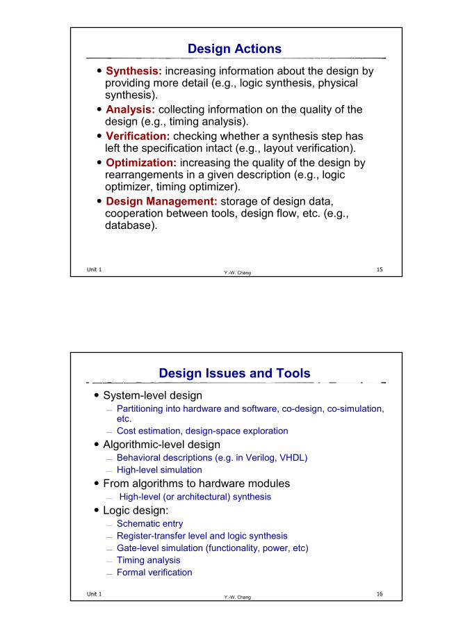
Design Actions˙Synthesis: increasing information about the design by
providing more detail (e.g., logic synthesis, physical synthesis).
˙Analysis: collecting information on the quality of the design (e.g., timing analysis).
˙Verification: checking whether a synthesis step has left the specification intact (e.g., layout verification).
˙Optimization: increasing the quality of the design by rearrangements in a given description (e.g., logic optimizer, timing optimizer).
˙Design Management: storage of design data, cooperation between tools, design flow, etc. (e.g., database).
Unit 1 16Y.-W. Chang
Design Issues and Tools˙System-level design
Partitioning into hardware and software, co-design, co-simulation, etc.
Cost estimation, design-space exploration˙Algorithmic-level design
Behavioral descriptions (e.g. in Verilog, VHDL) High-level simulation
˙From algorithms to hardware modules High-level (or architectural) synthesis
˙Logic design: Schematic entry Register-transfer level and logic synthesis Gate-level simulation (functionality, power, etc) Timing analysis Formal verification
9
Unit 1 17Y.-W. Chang
Logic Design/Synthesis
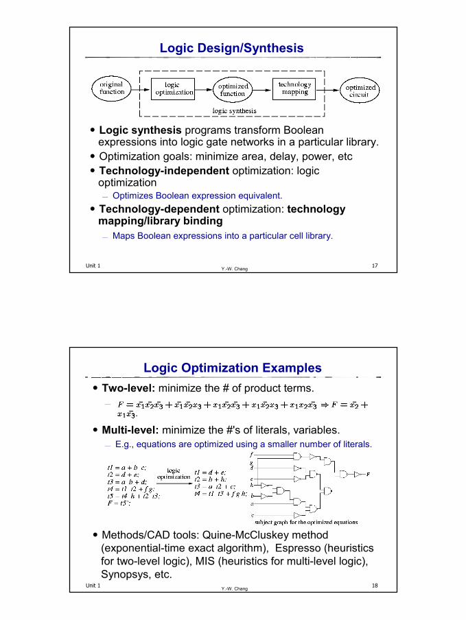
˙Logic synthesis programs transform Boolean expressions into logic gate networks in a particular library.
˙Optimization goals: minimize area, delay, power, etc˙Technology-independent optimization: logic
optimization Optimizes Boolean expression equivalent.
˙Technology-dependent optimization: technology mapping/library binding Maps Boolean expressions into a particular cell library.
Unit 1 18Y.-W. Chang
Logic Optimization Examples˙Two-level: minimize the # of product terms.
˙Multi-level: minimize the #'s of literals, variables. E.g., equations are optimized using a smaller number of literals.
˙Methods/CAD tools: Quine-McCluskey method (exponential-time exact algorithm), Espresso (heuristics for two-level logic), MIS (heuristics for multi-level logic), Synopsys, etc.
10
Unit 1 19Y.-W. Chang
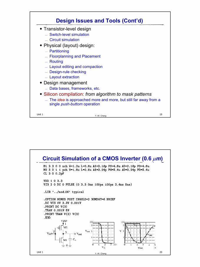
Design Issues and Tools (Cont’d)˙Transistor-level design
Switch-level simulation Circuit simulation
˙Physical (layout) design: Partitioning Floorplanning and Placement Routing Layout editing and compaction Design-rule checking Layout extraction
˙Design management Data bases, frameworks, etc.
˙Silicon compilation: from algorithm to mask patterns The idea is approached more and more, but still far away from a
single push-buttom operation
Unit 1 20Y.-W. Chang
Circuit Simulation of a CMOS Inverter (0.6 µm)
11
Unit 1 21Y.-W. Chang
Physical Design
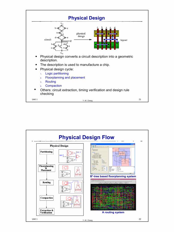
˙ Physical design converts a circuit description into a geometric description.
˙ The description is used to manufacture a chip. ˙ Physical design cycle:
1. Logic partitioning2. Floorplanning and placement3. Routing4. Compaction
• Others: circuit extraction, timing verification and design rule checking
Unit 1 22Y.-W. Chang
Physical Design Flow
B*-tree based floorplanning system
A routing system
12
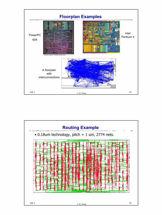
Unit 1 23Y.-W. Chang
Floorplan ExamplesPentium
4
PowerPC 604
Intel Pentium 4
A floorplanwith
interconnections
Unit 1 24Y.-W. Chang
Routing Example• 0.18um technology, pitch = 1 um, 2774 nets.
13
Unit 1 25Y.-W. Chang
IC Design Considerations
˙Several conflicting considerations: Design Complexity: large number of devices/transistors Performance: optimization requirements for high performance Time-to-market: about a 15% gain for early birds Cost: die area, packaging, testing, etc. Others: power, signal integrity (noise, etc), testability, reliability,
manufacturability, etc.
Unit 1 26Y.-W. Chang
4004 80386 PentiumPro8086 Pentium 4
Intel uP
˙Logic capacity doubles per IC at a regular interval.˙Moore: Logic capacity doubles per IC every two years (1975).˙D. House: Computer performance doubles every 18 months
(1975)
“Moore’s” Law: Driving Technology Advances
4Gb
14
Unit 1 27Y.-W. Chang
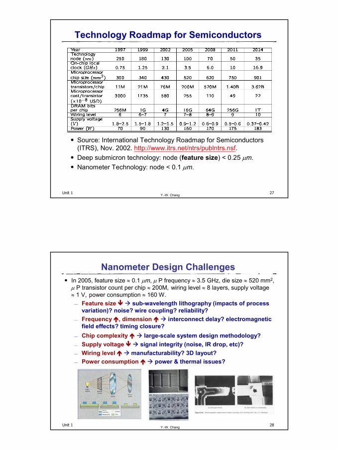
Technology Roadmap for Semiconductors
˙Source: International Technology Roadmap for Semiconductors (ITRS), Nov. 2002. http://www.itrs.net/ntrs/publntrs.nsf.
˙Deep submicron technology: node (feature size) < 0.25 µm.˙Nanometer Technology: node < 0.1 µm.
Unit 1 28Y.-W. Chang
Nanometer Design Challenges˙ In 2005, feature size ≈ 0.1 µm, µ P frequency ≈ 3.5 GHz, die size ≈ 520 mm2,
µ P transistor count per chip ≈ 200M, wiring level ≈ 8 layers, supply voltage ≈ 1 V, power consumption ≈ 160 W. Feature size sub-wavelength lithography (impacts of process
variation)? noise? wire coupling? reliability? Frequency , dimension interconnect delay? electromagnetic
field effects? timing closure? Chip complexity large-scale system design methodology? Supply voltage signal integrity (noise, IR drop, etc)? Wiring level manufacturability? 3D layout? Power consumption power & thermal issues?
15
Unit 1 29Y.-W. Chang
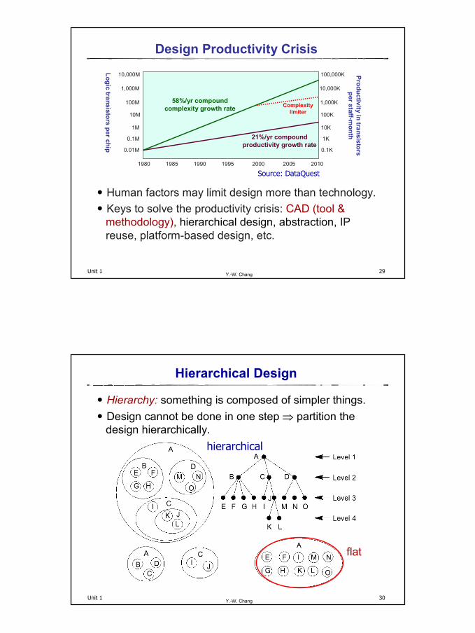
Design Productivity Crisis
˙Human factors may limit design more than technology.˙Keys to solve the productivity crisis: CAD (tool &
methodology), hierarchical design, abstraction, IP reuse, platform-based design, etc.
1980 1985 1990 2000 20101995 2005
0.01M
0.1M
1M
10M
100M
1,000M
10,000MLogic transistors per chip 0.1K
1K
10K
100K
1,000K
10,000K
100,000K Productivity in transistors per staff-m
onth21%/yr compound productivity growth rate
58%/yr compound complexity growth rate Complexity
limiter
Source: DataQuest
Unit 1 30Y.-W. Chang
Hierarchical Design
˙Hierarchy: something is composed of simpler things. ˙Design cannot be done in one step ⇒ partition the
design hierarchically.
flat
hierarchical
16
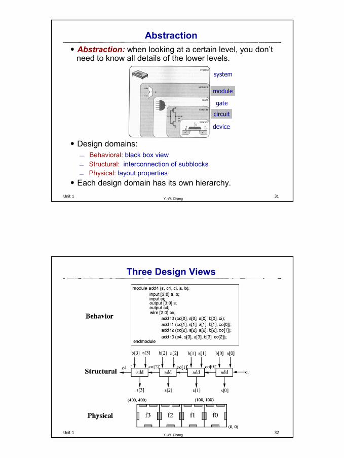
Unit 1 31Y.-W. Chang
Abstraction˙Abstraction: when looking at a certain level, you don’t
need to know all details of the lower levels.
˙Design domains: Behavioral: black box view Structural: interconnection of subblocks Physical: layout properties
˙Each design domain has its own hierarchy.
system
module
circuit
gate
device
Unit 1 32Y.-W. Chang
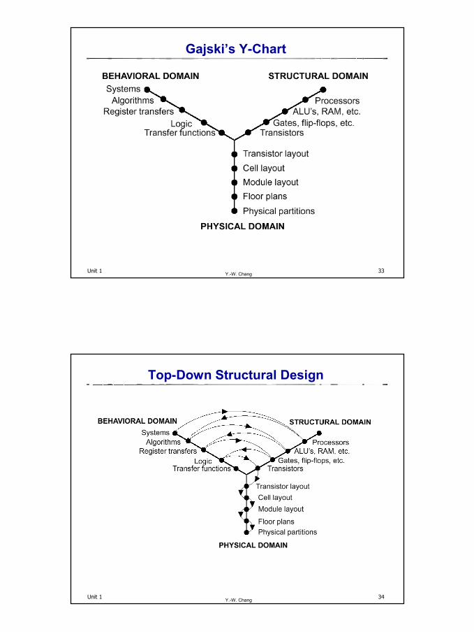
Three Design Views
17
Unit 1 33Y.-W. Chang
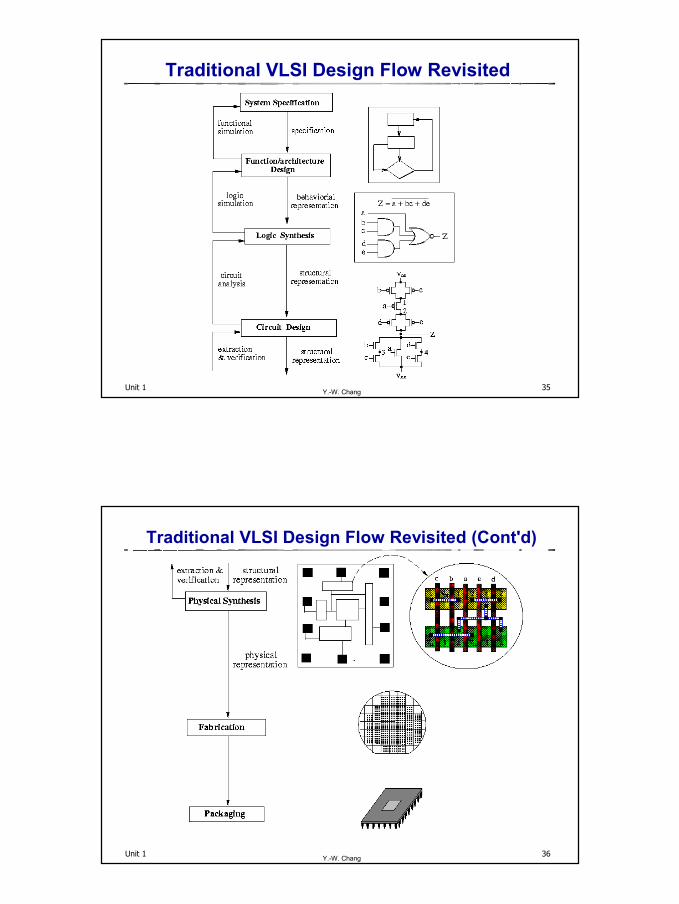
Gajski’s Y-Chart
Unit 1 34Y.-W. Chang
Top-Down Structural Design
18
Unit 1 35Y.-W. Chang
Traditional VLSI Design Flow Revisited
Unit 1 36Y.-W. Chang
Traditional VLSI Design Flow Revisited (Cont'd)
19
Unit 1 37Y.-W. Chang
Design Styles˙Specific design styles shall require specific CAD tools
Unit 1 38Y.-W. Chang
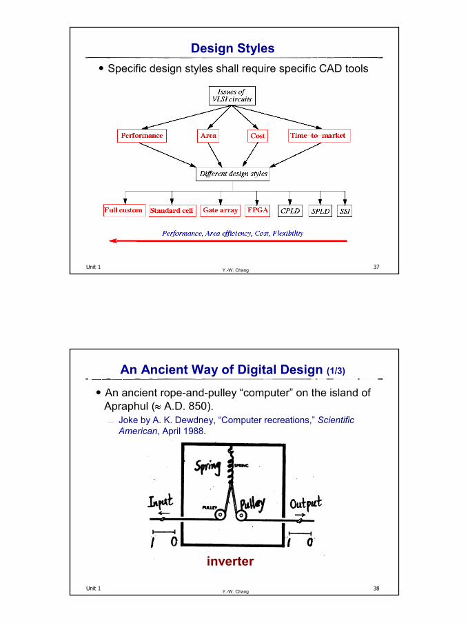
An Ancient Way of Digital Design (1/3)
˙An ancient rope-and-pulley “computer” on the island of Apraphul (≈ A.D. 850). Joke by A. K. Dewdney, “Computer recreations,” Scientific
American, April 1988.
inverter
20
Unit 1 39Y.-W. Chang
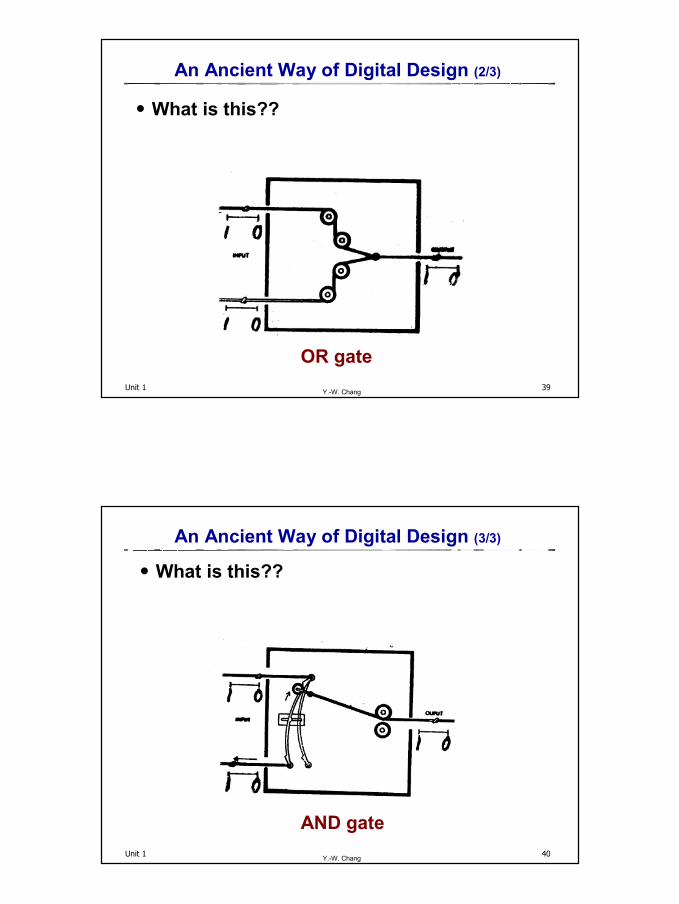
An Ancient Way of Digital Design (2/3)
˙What is this??
OR gate
Unit 1 40Y.-W. Chang
An Ancient Way of Digital Design (3/3)
˙What is this??
AND gate
21
Unit 1 41Y.-W. Chang
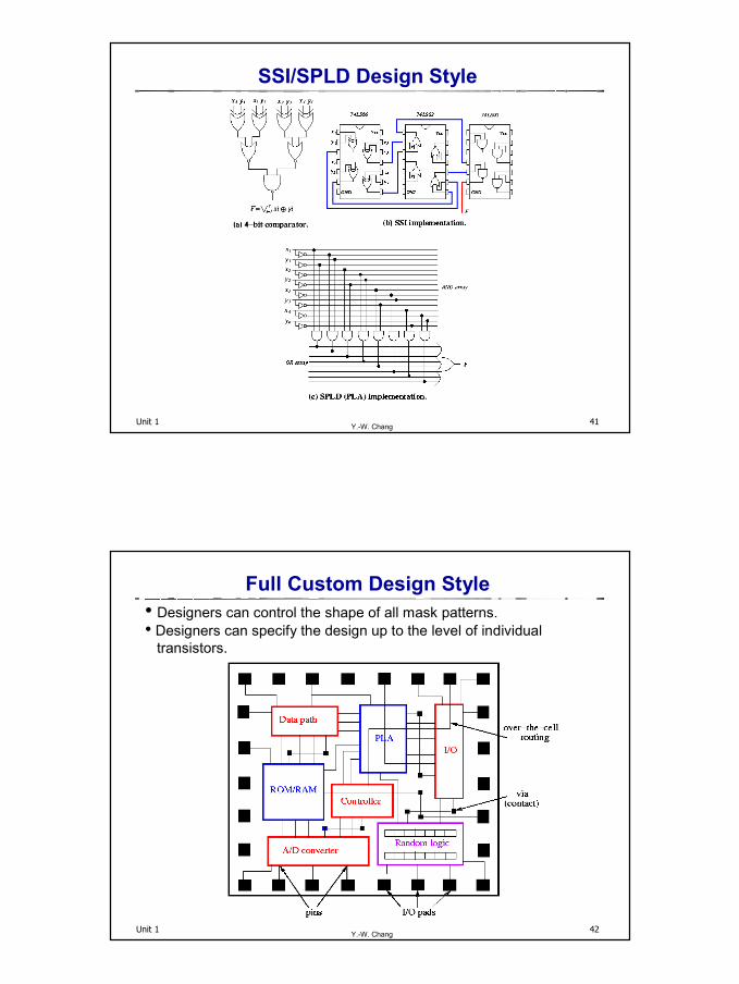
SSI/SPLD Design Style
Unit 1 42Y.-W. Chang
Full Custom Design Style• Designers can control the shape of all mask patterns.• Designers can specify the design up to the level of individual
transistors.
22
Unit 1 43Y.-W. Chang
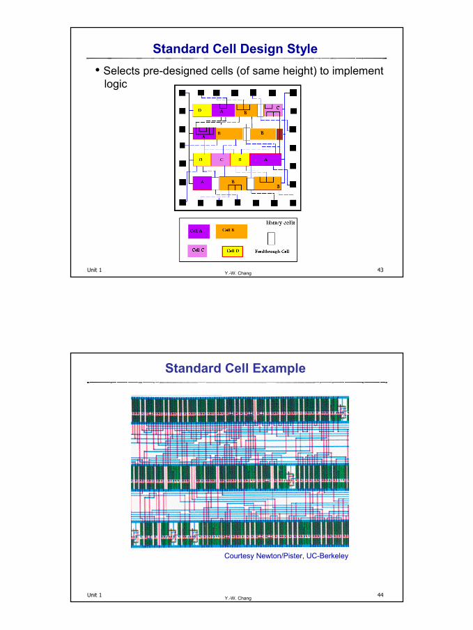
Standard Cell Design Style• Selects pre-designed cells (of same height) to implement
logic
Unit 1 44Y.-W. Chang
Standard Cell Example
Courtesy Newton/Pister, UC-Berkeley
23
Unit 1 45Y.-W. Chang
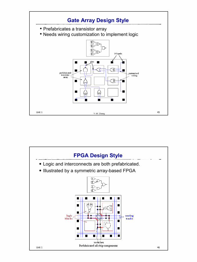
Gate Array Design Style• Prefabricates a transistor array• Needs wiring customization to implement logic
Unit 1 46Y.-W. Chang
FPGA Design Style˙Logic and interconnects are both prefabricated.˙Illustrated by a symmetric array-based FPGA
24
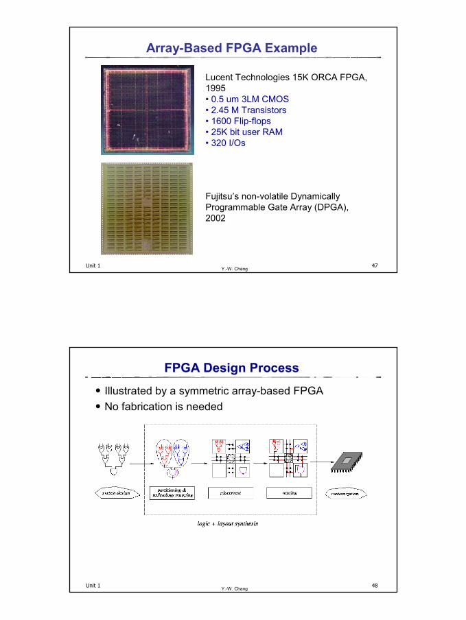
Unit 1 47Y.-W. Chang
Array-Based FPGA Example
Lucent Technologies 15K ORCA FPGA, 1995• 0.5 um 3LM CMOS• 2.45 M Transistors• 1600 Flip-flops• 25K bit user RAM• 320 I/Os
Fujitsu’s non-volatile Dynamically Programmable Gate Array (DPGA), 2002
Unit 1 48Y.-W. Chang
FPGA Design Process˙Illustrated by a symmetric array-based FPGA˙No fabrication is needed
25
Unit 1 49Y.-W. Chang
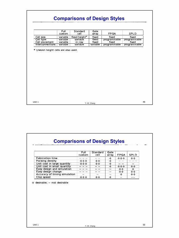
Comparisons of Design Styles
Unit 1 50Y.-W. Chang
Comparisons of Design Styles
26
Unit 1 51Y.-W. Chang
Design Style Trade-offs
Unit 1 52Y.-W. Chang
Upcoming: Structured ASIC˙A structured ASIC
consists of predefined metal and via layers, as well as a few of them for customization.
˙The predefined layers support power distribution and local communications among the building blocks of the device.
˙Advantages: fewer masks (lower cost) ; easier physical extraction and analysis.
Green blocks: I/C cells and other hard macro blocksBlue area: standard cellsWhite points: the spare cells
A structured ASIC (M5 & M6 can be customized)
27
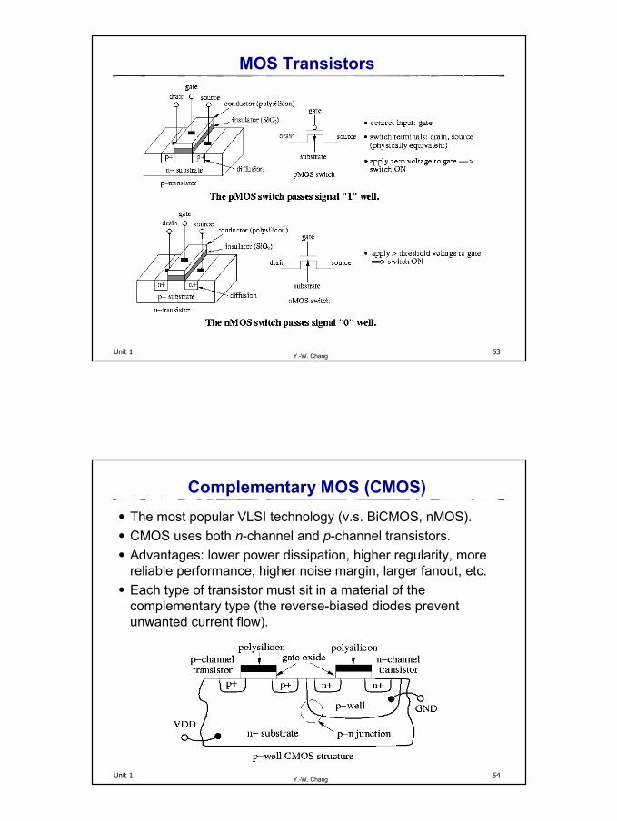
Unit 1 53Y.-W. Chang
MOS Transistors
Unit 1 54Y.-W. Chang
Complementary MOS (CMOS)˙The most popular VLSI technology (v.s. BiCMOS, nMOS).˙CMOS uses both n-channel and p-channel transistors.˙Advantages: lower power dissipation, higher regularity, more
reliable performance, higher noise margin, larger fanout, etc. ˙Each type of transistor must sit in a material of the
complementary type (the reverse-biased diodes prevent unwanted current flow).
28
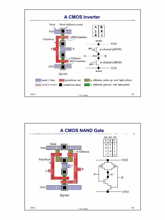
Unit 1 55Y.-W. Chang
A CMOS Inverter
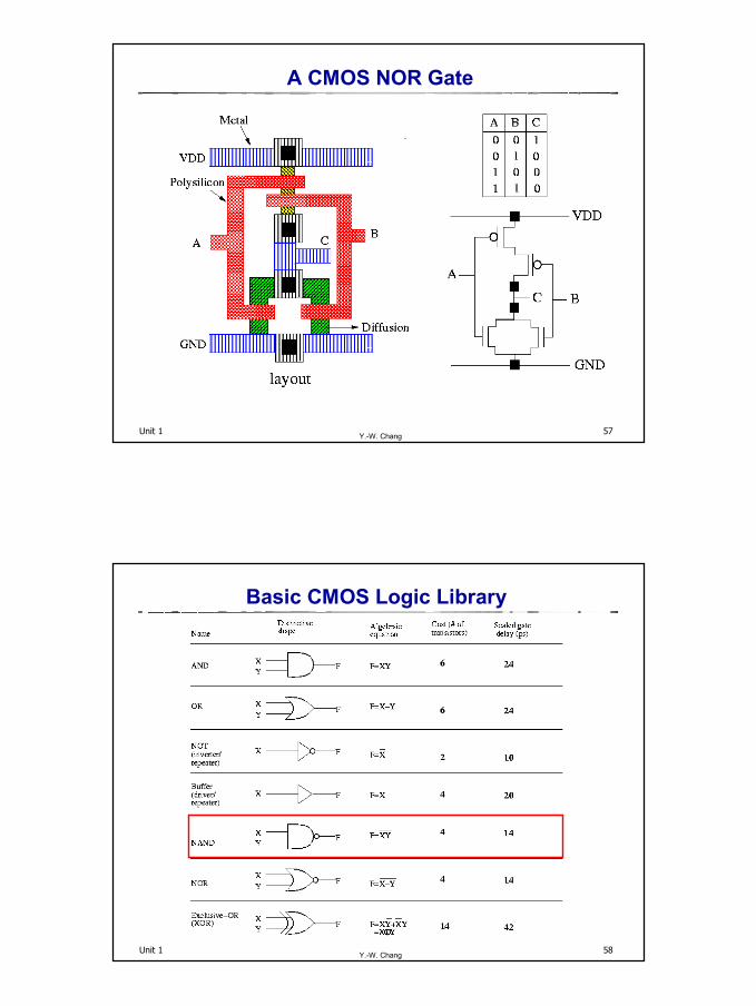
Unit 1 56Y.-W. Chang
A CMOS NAND Gate
29
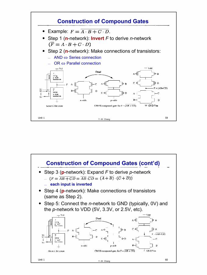
Unit 1 57Y.-W. Chang
A CMOS NOR Gate
Unit 1 58Y.-W. Chang
Basic CMOS Logic Library
30
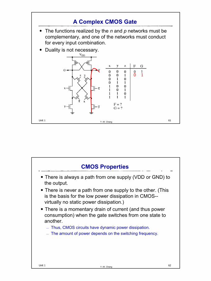
Unit 1 59Y.-W. Chang
Construction of Compound Gates˙ Example: ˙ Step 1 (n-network): Invert F to derive n-network
˙ Step 2 (n-network): Make connections of transistors: AND ⇔ Series connection OR ⇔ Parallel connection
Unit 1 60Y.-W. Chang
Construction of Compound Gates (cont’d)˙ Step 3 (p-network): Expand F to derive p-network
each input is inverted˙ Step 4 (p-network): Make connections of transistors
(same as Step 2).˙ Step 5: Connect the n-network to GND (typically, 0V) and
the p-network to VDD (5V, 3.3V, or 2.5V, etc).
31
Unit 1 61Y.-W. Chang
A Complex CMOS Gate˙ The functions realized by the n and p networks must be
complementary, and one of the networks must conduct for every input combination.
˙ Duality is not necessary.
0 1
Unit 1 62Y.-W. Chang
CMOS Properties˙There is always a path from one supply (VDD or GND) to
the output.˙There is never a path from one supply to the other. (This
is the basis for the low power dissipation in CMOS--virtually no static power dissipation.)
˙There is a momentary drain of current (and thus power consumption) when the gate switches from one state to another. Thus, CMOS circuits have dynamic power dissipation. The amount of power depends on the switching frequency.
32
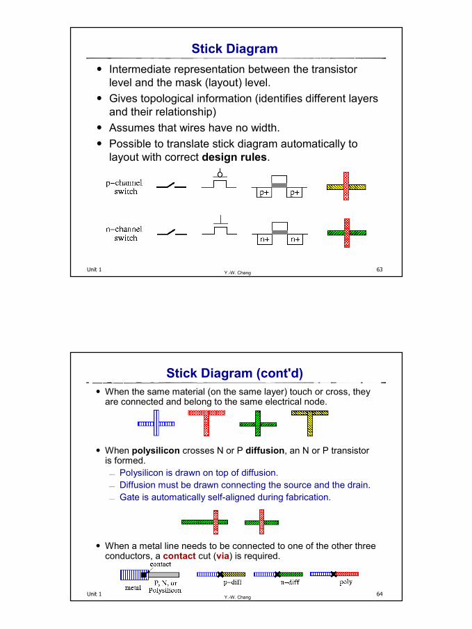
Unit 1 63Y.-W. Chang
Stick Diagram˙ Intermediate representation between the transistor
level and the mask (layout) level. ˙ Gives topological information (identifies different layers
and their relationship)˙ Assumes that wires have no width.˙ Possible to translate stick diagram automatically to
layout with correct design rules.
Unit 1 64Y.-W. Chang
Stick Diagram (cont'd)˙When the same material (on the same layer) touch or cross, they
are connected and belong to the same electrical node.
˙When polysilicon crosses N or P diffusion, an N or P transistor is formed. Polysilicon is drawn on top of diffusion. Diffusion must be drawn connecting the source and the drain. Gate is automatically self-aligned during fabrication.
˙When a metal line needs to be connected to one of the other three conductors, a contact cut (via) is required.
33
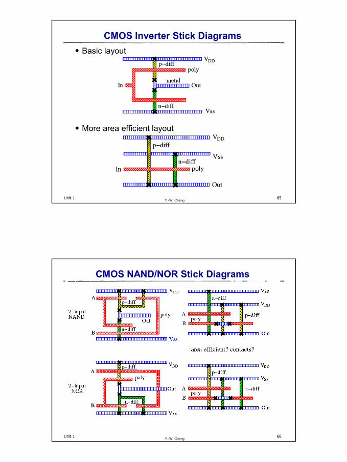
Unit 1 65Y.-W. Chang
CMOS Inverter Stick Diagrams˙Basic layout
˙More area efficient layout
Unit 1 66Y.-W. Chang
CMOS NAND/NOR Stick Diagrams
34
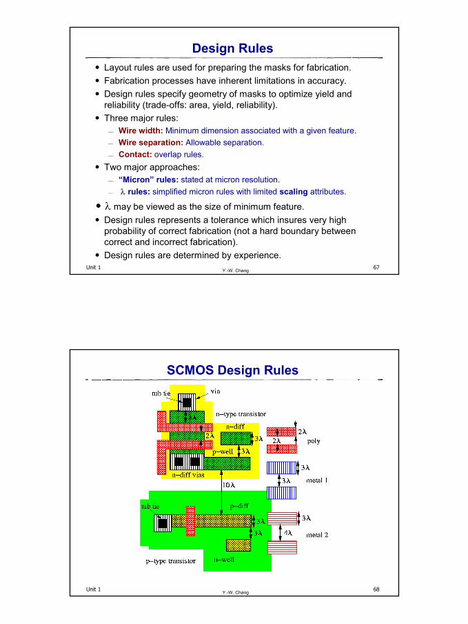
Unit 1 67Y.-W. Chang
Design Rules˙Layout rules are used for preparing the masks for fabrication.˙Fabrication processes have inherent limitations in accuracy.˙Design rules specify geometry of masks to optimize yield and
reliability (trade-offs: area, yield, reliability).˙Three major rules:
Wire width: Minimum dimension associated with a given feature. Wire separation: Allowable separation. Contact: overlap rules.
˙Two major approaches: “Micron” rules: stated at micron resolution. λ rules: simplified micron rules with limited scaling attributes.
˙λ may be viewed as the size of minimum feature.˙Design rules represents a tolerance which insures very high
probability of correct fabrication (not a hard boundary between correct and incorrect fabrication).
˙Design rules are determined by experience.
Unit 1 68Y.-W. Chang
SCMOS Design Rules
35
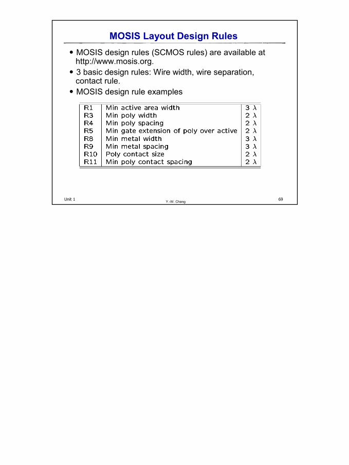
Unit 1 69Y.-W. Chang
MOSIS Layout Design Rules˙MOSIS design rules (SCMOS rules) are available at
http://www.mosis.org. ˙3 basic design rules: Wire width, wire separation,
contact rule.˙MOSIS design rule examples