Embed Size (px)
Citation preview
Page 537
VLSI Design and Implementation of High Speed and High
Throughput DADDA Multiplier
U.V.N.S.Suhitha
Student
Department of ECE,
BVC College of Engineering,
AP, India.
Mr.G.Ravikanth, M.Tech, (Ph.D)
Associate Professor,
Department of ECE,
BVC College of Engineering,
AP, India.
Abstract:
The ever growing need for improved security for
applications over internet has resulted in wide
acceptance of Elliptic Curve Cryptography (ECC) in
industry and academic research. This growth has started
the spread of architectures for implementing ECC from
FPGA towards ASIC. High speed multiplication is a
primary requirement of high performance digital
systems. The largest contribution to the power
consumption in a multiplier is due to generation and
reduction of partial products. Among multipliers, tree
multipliers are used in high speed applications such as
filters. This paper discusses the ASIC based
implementation of dadda multiplier. 16bit Dadda
multiplier is developed and compared with Redundant
Basis multiplier (high-throughput finite field multiplier
based on RB). The performance of the proposed
multiplier is analyzed by evaluating the delay and area.
Arithmetic components are designed using Verilog and
implemented using Xilinx ISE 13.2. The proposed
variation of dadda Multiplier has low power
considerations and better area delay product.
Keywords: ASIC, Dadda multiplier, finite field
multiplication, FPGA, Elliptic Curve Cryptography
(ECC)
I. INTRODUCTION
Finite field is a basic operation frequently ITE FIELD
multiplication [1] over Galois Field (GF(2m)) (encountered
in modern cryptographic systems such as the elliptic curve
cryptography (ECC) and error control coding [2]–[3].
Moreover, multiplication over a finite field can be used
further to perform other field operations, e.g., division,
exponentiation, and inversion. [5]–[7] Multiplication over
can be implemented on a general purpose machine, but it
is expensive to use a general purpose machine to
implement cryptographic systems in cost-sensitive
consumer products. Besides, a low-end Microprocessor
cannot meet the real-time requirement of different
applications since word length of these processors is too
small compared with the order of typical finite fields used
in cryptographic systems. Most of the real-time
applications, therefore, need hardware implementation [6]
–[8] of finite field arithmetic operations for the benefits
like low-cost and high-throughput rate.
In this paper, we aim to developed 16 bit Dadda multiplier
and compared with Redundant Basics multiplier (high-
throughput finite field multiplication over based on RB)
2-dimensional signal- flow graph (SFG) array, followed
by suitable projection of SFG to 1-dimensional processor-
space flow graph (PSFG), and the choice of feed-forward
cut-set to enhance the throughput rate. [8] Our proposed
dadda multiplier involves significantly less area-time
complexities than the corresponding existing designs.
Field programmable gate array (FPGA) has evolved as a
mainstream dedicated computing platform.

Page 538
II. Derivation of High throughput Structures for
RB Multipliers
Architecture-I
Fig. 1. Signal- flow graph (SFG) for parallel realization of
RB multiplication. (a) The SFG. (b) Functional
description of S node, where S-I node performs circular
bit-shifting of one position and S-II node performs circular
bit-shifting by positions. (c) Functional description of M
node. (d) Functional description of A node.
According to (11) and (12), The RB multiplication can be
represented by the 2-dimensional SFG (shown in Fig. 1)
consisting of parallel arrays, where each array consists of
bit-shifting nodes (S node), multiplication nodes (M
nodes) and addition nodes (A nodes). There are two types
of S nodes (S-I node and S-II node). Function of S nodes
is depicted in Fig. 1(b), where S-I node performs circular
bit-shifting by one position and S-II node performs
circular bit-shifting by positions for the degree
reduction requirement. Functions of M nodes and A nodes
are depicted in Fig. 1(c) and 1(d), respectively. Each of
the M nodes performs an AND operation of a bit of serial-
input operand with bit-shifted form of operand , while
each of the A nodes performs an XOR operation. The final
addition of the output of arrays of Fig. 1 can be performed
by bit-by-bit XOR of the operands in number of A nodes
as depicted in Fig. 1. The desired product word is obtained
after the addition of parallel output of the arrays
Fig. 2. Processor-Space flow graph (PSFG) of digit-
serial realization of finite field RB multiplication over . (a)
The proposed PSFG. (b) Functional description of add-
accumulation (AA) node.
For digit-serial realization of RB multiplier, the SFG of
Fig. 1 can be projected along -direction to obtain a PSFG
as shown in Fig. 2, where input bits are loaded in parallel
to multiplication nodes during each cycle period. The
functions of nodes of PSFG are the same as those of
corresponding nodes in the SFG of Fig. 1 except an extra
add-accumulation (AA) node. The function of the AA
node is, as described in Fig. 2(b), to execute the
accumulation operation for cycles to yield the desired
result thereafter.
Fig. 3. Cut-set retiming of PSFG of finite field RB
multiplication over (GF(2m)) Where “D ” denotes delay

Page 539
For efficient realization of a digit-serial RB multiplier, we
can perform feed-forward cut-set retiming in a regular
interval in the PSFG as shown in Fig. 3. As a result of cut-
set retiming of the Fig. 3, the minimum duration of each
clock period is reduced to(TA+TB) , where and denote the
delay of an AND gate and an XOR gate, respectively
Fig.4 . structure - I for RB multiplier when . (a) cut-set
retiming of PSFG when . (b) Detailed internal structure of
merged regular PPGU. (c) Corresponding architecture-I
for the case.
For example, to obtain the proposed structure for d=2 , a
pair of S nodes, a pair of M nodes and a pair of A nodes of
the PSFG of Fig. 3 can be merged to form a macro-node
as shown within the dashed-lines in Fig.4. Each of these
macro nodes can be implemented by a new PPGU to
obtain a PPGM of p/2 PPGUs as shown in Fig.4(b), which
consists of two AND cells and two XOR cells (the first
PPGU requires only one XOR cell). The AND cell, XOR
cell and register cell of PPGM perform the function of M
node, A node and delay imposed by the retiming of PSFG
of Fig. 3, respectively. Structures and functions of AND
cell, XOR cell and register cell are shown in
Fig.4(c),(d),and (e), respectively. The first output of
desired product is available from this structure after a
latency of cycles, while the successive outputs are
available thereafter in each cycles of duration. The
technique used to derive the structure for may be extended
for any value of, to obtain a structure consisting of
PPGUs.
Architecture-II
We can further transform the PSFG of Fig. 3 to reduce the
latency and hardware complexity of architecture-I. To
obtain the proposed structure, serially-connected A nodes
of the PSFG of Fig. 3 are merged into a pipeline form of A
nodes as shown within the dashed-box in Fig. 5(a). These
pipelined A nodes can be implemented by a pipelined
XOR tree, as shown in Fig. 5(b). Since all the AND cells
can be processed in parallel, there is no need of using
extra “0”s on the input path to meet the timing
requirement in systolic pipeline. The critical path and
throughput of architecture-II are the same as those of
architecture -I. Similarly, arch -II can be easily extended
to larger values of to have low register-complexity
structures.

Page 540
Fig.5. structure-II for RB multiplier, where “R” denotes a
register cell. (a) Modified PSFG. (b) Structure of RB
multiplier
Architecture-III
Since the S nodes of Fig. 3 perform only the bit-shifting
operations they do not involve any time consumption.
Therefore, we can introduce a novel cut-set retiming to
reduce the critical path further, as shown in Fig. 6(a). It
can be observed that the cut-set retiming allows to
perform the bit-addition and bit-multiplication
concurrently, so that the critical-path is reduced to
max{TA+TX}=TX, i.e. the throughput of the design Is
increased.
Fig.6. Novel cut-set retiming of PSFG and its
corresponding structure: Structure-III.
(a) Cut-set retiming. (b) BPM and PPGM of Structure-III.
The proposed system can be done using Dadda multiplier,
by using this delay will be reduced.The process of Dadda
multiplication is as follows:
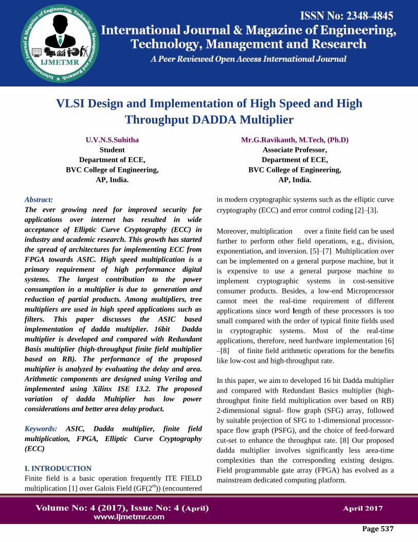
The entire 16 × 16 multiplication requires six stages.
Always the first stage is partial products stage, which is
obtained by simple multiplication of multiplicand with
multiplier. The number of rows (height) present at this
stage is 16. Now reduce the number of rows further in
such a way that final stage contains only two rows. For
this, Dadda introduces a sequence of intermediate matrix
heights that provides the minimum number of reduction
stages for a given size multiplier. This sequence
determined by working back from the final two row
matrix, limit the height of each intermediate matrix to the
largest integer that is no more than 1.5 times the height of
its successor.
Page 541
Fig.7.Dot diagram of 16-bit Dadda multiplier
RESULTS:
The written Verilog HDL Modules have been successfully
simulated, verified and synthesized using Xilinx ISE13.2.
The delay values clearly indicate that the proposed
multiplier is always faster than the regular RB multiplier.
PERFORMANCE OF THE DADDA MULTIPLIER
WITH REFERENCE TO THE RB MULTIPLIER:
It exhibits that the area of the regular Dadda multiplier is
only slightly lesser, ranging from 11% to 10% for the 16-
bit, than the area of the redundant basis multiplier. The
delay values clearly indicate that the proposed multiplier
is always faster than the regular RB multiplier.
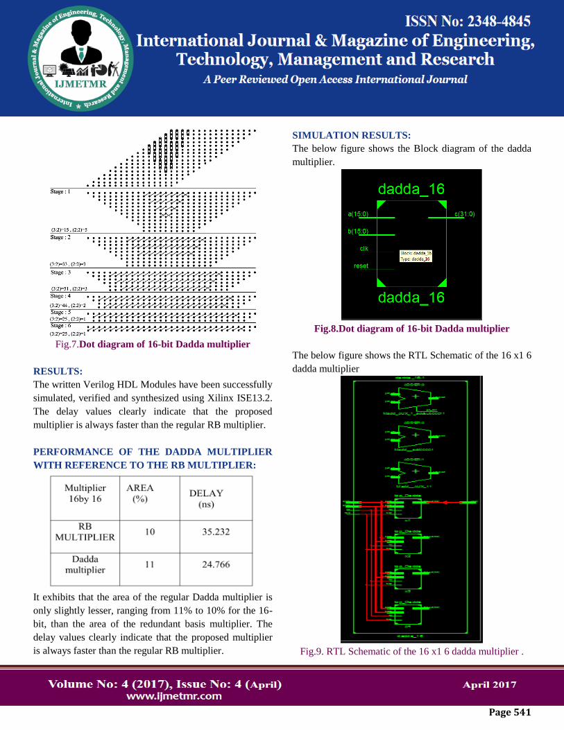
SIMULATION RESULTS:
The below figure shows the Block diagram of the dadda
multiplier.
Fig.8.Dot diagram of 16-bit Dadda multiplier
The below figure shows the RTL Schematic of the 16 x1 6
dadda multiplier
Fig.9. RTL Schematic of the 16 x1 6 dadda multiplier .

Page 542
Simulation output waveform of the dadda multiplier:
Fig.10. Output Waveform Of The Dadda Multiplier.
CONCLUSION:
Finite field multipliers play a very important role in the
areas of digital communication especially in the areas of
cryptography, error control coding and digital signal
processing. In this paper, two multipliers namely
Redundant Basics multilpier and dadda multipliers were
simulated. The comparison results show that dadda
multiplier is more efficient than the other multiplier.
Using dadda multiplier we can improve the performance
of the process. The dadda multiplier algorithm is an
optimization technique used for decomposing larger
multiplications into multiple smaller multiplications. This
feature allows the multiplier to be scaled easily.
The analysis of the results shows that the speed and area
improvements are significant compared to the regular RB
multiplier.
The proposed multiplier design technique can be
implemented with any type of parallel multipliers to
achieve faster performance.
REFERENCES
[1] High-Throughput Finite Field Multipliers Using
Redundant Basis for FPGA and ASIC Implementations.
Jiafeng Xie, Pramod Kumar Meher, Senior Member,
IEEE, and Zhi-Hong Mao, Senior Member,IEEE
[2] I. Blake, G. Seroussi, and N. P. Smart, Elliptic Curves
in Cryptography, ser. London Mathematical Society
Lecture Note Series.. Cambridge, U.K.: Cambridge Univ.
Press, 1999
[3] N. R. Murthy and M. N. S. Swamy, “Cryptographic
applications of brahmaqupta-bhaskara equation,” IEEE
Trans. Circuits Syst. I, Reg. Papers, vol. 53, no. 7, pp.
1565–1571,2006.
[4] L. Song and K. K. Parhi, “Low-energy digit-
serial/parallel finite field multipliers,” J. VLSI Digit.
Process., vol. 19, pp. 149–C166, 1998.
[5] P. K. Meher, “On implementation of accumulation
in finite field over and its applications,” IEEE Trans. Very
Large Scale Integr. (VLSI) Syst., vol. 17, no. 4, pp. 541–
550,2009.
[6] L. Song, K. K. Parhi, I. Kuroda, and T. Nishitani,
“Hardware/software codesign of finite field datapath for
low-energy Reed-Solomn codecs,” IEEE Trans. Very
Large Scale Integr.(VLSI) Syst., vol.8,no.2,pp. 160–
172,Apr.2000.
[7] G. Drolet, “A new representation of elements of finite
fields yielding small complexity arithmetic circuits,” IEEE
Trans. Comput., vol. 47, no. 9, pp. 938–946, 1998.
[8] C.-Y. Lee, J.-S. Horng, I.-C. Jou, and E.-
H.Lu,“Low-complexity bit-parallelsystolic montgomery
multipliers for special classes of ,” IEEE Trans.
Comput., vol. 54, no. 9, pp.1061–1070,Sep.2005.

Page 543
[9] P. K. Meher, “Systolic and super-systolic multipliers
for finite field based on irreducible trinomials,” IEEE
Trans. Circuits Syst. I, Reg. Papers,vol.55,no.4, pp.1031–
1040,May2008.
[10] H. Wu, M. A. Hasan, I. F. Blake, and S. Gao, “Finite
field multiplier using redundant representation,” IEEE
Trans. Comput., vol. 51,no.11,pp.1306–1316,Nov.2002.
[11] A. H. Namin, H. Wu, and M. Ahmadi, “A new finite
field multiplier using redundat representation,” IEEE
Trans. Comput., vol. 57, no. 5,pp. 716–720, May 2008.
[12] A. H. Namin, H.Wu, and M. Ahmadi, “A high-speed
word level finite field multiplier in using redundant
representation,” IEEE Trans.Very Large Scale Integr.
(VLSI) Syst., vol. 17, no. 10, pp. 1546–1550,Oct. 2009.