Embed Size (px)
Citation preview
Funding Sources
VLSI CAD Laboratory CSE & ECE Departments, UC San Diego
SRC NSF IMPACT+ Qualcomm Samsung NXP Sandia
Research Areas http://vlsicad.ucsd.edu/
Faculty Prof. Andrew B. Kahng Students Tuck-Boon Chan (5th Yr)
Vaishnav Srinivas (4th Yr)
Siddhartha Nath (4th Yr)
Wei-Ting Jonas Chan (3rd Yr)
Jiajia Li (3rd Yr)
Hyein Lee (2nd Yr)
Ilgweon Kang (2nd Yr)
Kwangsoo Han (1st Yr)
Visitors Dr. Jae-Gon Lee (Samsung)
Prof. Seung-Soo Han (Myongji University)
http://vlsicad.ucsd.edu/
Design for Manufacturability (DFM)
Technology Roadmap (ITRS)
Adaptive and Resilient Circuits
3D Integrated Circuit Design
IC Physical Design
Modeling and Estimation
Design Margin Reduction and Signoff
Infrastructure (standards, open-source)
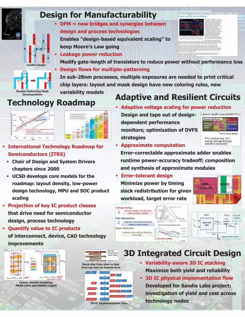
� DFM = new bridges and synergies between design and process technologies Enables “design-based equivalent scaling” to keep Moore’s Law going
� Leakage power reduction
Design for Manufacturability
Technology Roadmap
� International Technology Roadmap for Semiconductors (ITRS) � Chair of Design and System Drivers
chapters since 2000 � UCSD develops core models for the
roadmap: layout density, low-power design technology, MPU and SOC product scaling
� Projection of key IC product classes that drive need for semiconductor design, process technology
� Quantify value to IC products of interconnect, device, CAD technology improvements
Adaptive and Resilient Circuits
3D Integrated Circuit Design � Variability-aware 3D IC stacking
Maximize both yield and reliability � 3D IC physical implementation flow
Developed for Sandia Labs project; investigation of yield and cost across technology nodes
� Adaptive voltage scaling for power reduction Design and tape out of design- dependent performance monitors; optimization of DVFS strategies
� Approximate computation Error-correctable approximate adder enables runtime power-accuracy tradeoff; composition and synthesis of approximate modules
� Error-tolerant design Minimize power by timing slack redistribution for given workload, target error rate
ARM Cortex M3
DDRO
Double-Patterning Mask Decomposition
Conflict Graph
accurate results
approximate results
Layout density modeling: SRAM (left) and NAND2 (right)
3D-IC Implementation Flow
Stack dies from slow to fast, from top tiers to bottom tiers
Modify gate-length of transistors to reduce power without performance loss � Design flows for multiple-patterning
In sub-28nm processes, multiple exposures are needed to print critical chip layers: layout and mask design have new coloring rules, new variability models
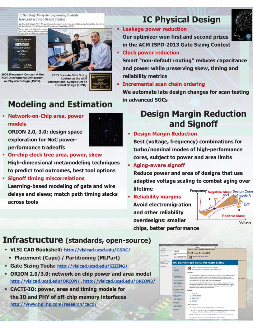
Modeling and Estimation � Network-on-Chip area, power
models ORION 2.0, 3.0: design space exploration for NoC power-performance tradeoffs
Infrastructure (standards, open-source) � VLSI CAD Bookshelf: http://vlsicad.ucsd.edu/GSRC/
� Placement (Capo) / Partitioning (MLPart) � Gate Sizing Tools: http://vlsicad.ucsd.edu/SIZING/
� ORION 2.0/3.0: network on chip power and area model http://vlsicad.ucsd.edu/ORION/ , http://vlsicad.ucsd.edu/ORION3/
� Leakage power reduction Our optimizer won first and second prizes in the ACM ISPD-2013 Gate Sizing Contest
� Clock power reduction Smart “non-default routing” reduces capacitance and power while preserving skew, timing and reliability metrics
� Incremental scan chain ordering We automate late design changes for scan testing in advanced SOCs
IC Physical Design
2013 Discrete Gate Sizing Contest at the ACM
International Symposium on Physical Design (ISPD).
Design Margin Reduction and Signoff
� On-chip clock tree area, power, skew High-dimensional metamodeling techniques to predict tool outcomes, best tool options
� Signoff timing miscorrelations Learning-based modeling of gate and wire delays and slews; match path timing slacks across tools
� CACTI-IO: power, area and timing models for the IO and PHY of off-chip memory interfaces http://www.hpl.hp.com/research/cacti/
LVT
HVT
Voltage
Frequency
A
Design Cone of mode A
C
Negative Slack
Positive Slack
B
� Design Margin Reduction Best (voltage, frequency) combinations for turbo/nominal modes of high-performance cores, subject to power and area limits
� Aging-aware signoff Reduce power and area of designs that use adaptive voltage scaling to combat aging over lifetime
� Reliability margins Avoid electromigration and other reliability overdesigns: smaller chips, better performance
2005 Placement Contest at the ACM International Symposium
on Physical Design (ISPD).