Embed Size (px)
Citation preview

Vivado Design Suite User Guide
Programming and Debugging
UG908 (v2013.2) September 13, 2013
Vivado Programming and Debugging www.xilinx.com 2UG908 (v2013.2) September 13, 2013
Notice of DisclaimerThe information disclosed to you hereunder (the “Materials”) is provided solely for the selection and use of Xilinx products. To the maximum extent permitted by applicable law: (1) Materials are made available "AS IS" and with all faults, Xilinx hereby DISCLAIMS ALL WARRANTIES AND CONDITIONS, EXPRESS, IMPLIED, OR STATUTORY, INCLUDING BUT NOT LIMITED TO WARRANTIES OF MERCHANTABILITY, NON-INFRINGEMENT, OR FITNESS FOR ANY PARTICULAR PURPOSE; and (2) Xilinx shall not be liable (whether in contract or tort, including negligence, or under any other theory of liability) for any loss or damage of any kind or nature related to, arising under, or in connection with, the Materials (including your use of the Materials), including for any direct, indirect, special, incidental, or consequential loss or damage (including loss of data, profits, goodwill, or any type of loss or damage suffered as a result of any action brought by a third party) even if such damage or loss was reasonably foreseeable or Xilinx had been advised of the possibility of the same. Xilinx assumes no obligation to correct any errors contained in the Materials or to notify you of updates to the Materials or to product specifications. You may not reproduce, modify, distribute, or publicly display the Materials without prior written consent. Certain products are subject to the terms and conditions of the Limited Warranties which can be viewed at http://www.xilinx.com/warranty.htm; IP cores may be subject to warranty and support terms contained in a license issued to you by Xilinx. Xilinx products are not designed or intended to be fail-safe or for use in any application requiring fail-safe performance; you assume sole risk and liability for use of Xilinx products in Critical Applications: http://www.xilinx.com/warranty.htm#critapps.© Copyright 2012-2013 Xilinx, Inc. Xilinx, the Xilinx logo, Artix, ISE, Kintex, Spartan, Virtex, Vivado, Zynq, and other designated brands included herein are trademarks of Xilinx in the United States and other countries. All other trademarks are the property of their respective owners.
Revision HistoryThe following table shows the revision history for this document.
Date Version Revision
07/25/12 2012.2 Initial Xilinx release.
10/16/12 2012.3 Update to Bitstream settings.
12/18/12 2012.4 Added section for Waveform Configuration. Removed Waveform Viewer Limitations.
03/20/13 2013.1 • General updates for 2013.1. • New section on In-System Serial I/O Debugging. New section on Description of
hw_tcl Commands. • New table for New Debugging Cores in Vivado IP for use in HDL Instantiation
Flow
06/19/2013 2013.2 • Updated support for hw_server including TCF Agent. • Made various corrections and updates to reflect changes to the Vivado user
interface.
9/13/2013 2013.2 • Removed watermark
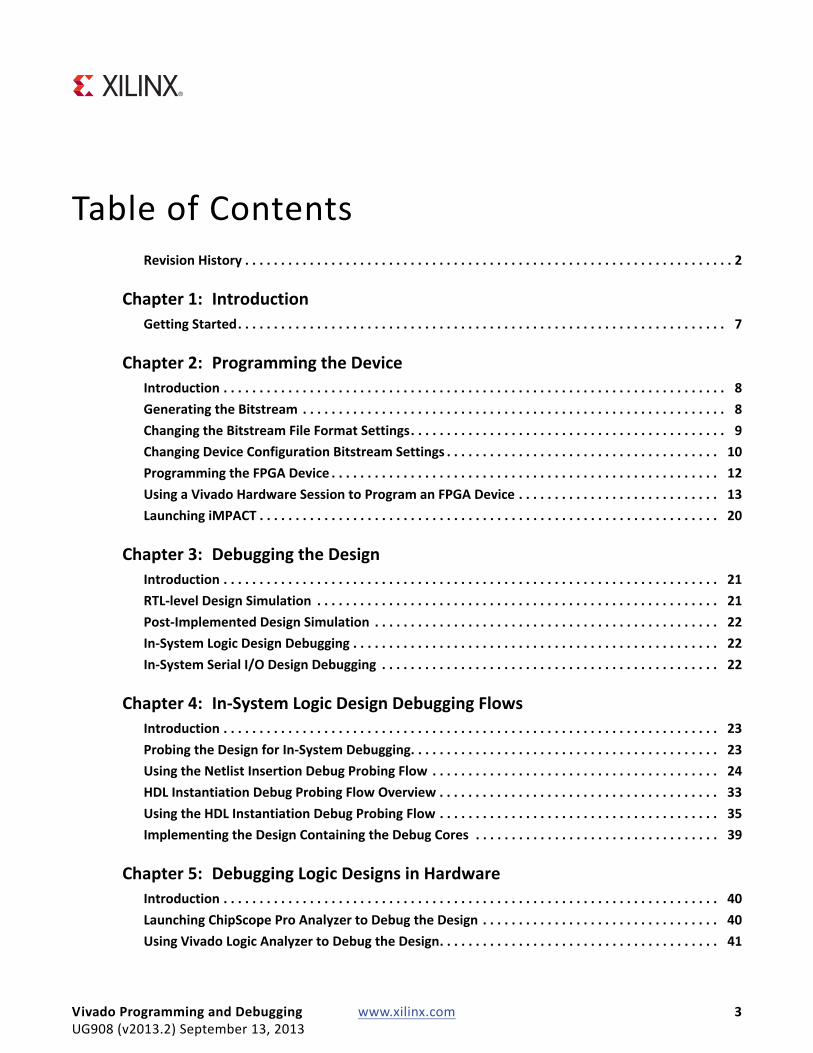
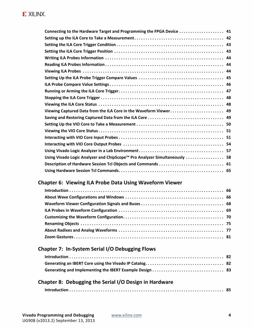
Table of ContentsRevision History . . . . . . . . . . . . . . . . . . . . . . . . . . . . . . . . . . . . . . . . . . . . . . . . . . . . . . . . . . . . . . . . . . . . 2
Chapter 1: IntroductionGetting Started. . . . . . . . . . . . . . . . . . . . . . . . . . . . . . . . . . . . . . . . . . . . . . . . . . . . . . . . . . . . . . . . . . . . 7
Chapter 2: Programming the DeviceIntroduction . . . . . . . . . . . . . . . . . . . . . . . . . . . . . . . . . . . . . . . . . . . . . . . . . . . . . . . . . . . . . . . . . . . . . . 8Generating the Bitstream . . . . . . . . . . . . . . . . . . . . . . . . . . . . . . . . . . . . . . . . . . . . . . . . . . . . . . . . . . . 8Changing the Bitstream File Format Settings. . . . . . . . . . . . . . . . . . . . . . . . . . . . . . . . . . . . . . . . . . . . 9Changing Device Configuration Bitstream Settings . . . . . . . . . . . . . . . . . . . . . . . . . . . . . . . . . . . . . . 10Programming the FPGA Device . . . . . . . . . . . . . . . . . . . . . . . . . . . . . . . . . . . . . . . . . . . . . . . . . . . . . . 12Using a Vivado Hardware Session to Program an FPGA Device . . . . . . . . . . . . . . . . . . . . . . . . . . . . 13Launching iMPACT . . . . . . . . . . . . . . . . . . . . . . . . . . . . . . . . . . . . . . . . . . . . . . . . . . . . . . . . . . . . . . . . 20
Chapter 3: Debugging the DesignIntroduction . . . . . . . . . . . . . . . . . . . . . . . . . . . . . . . . . . . . . . . . . . . . . . . . . . . . . . . . . . . . . . . . . . . . . 21RTL-level Design Simulation . . . . . . . . . . . . . . . . . . . . . . . . . . . . . . . . . . . . . . . . . . . . . . . . . . . . . . . . 21Post-Implemented Design Simulation . . . . . . . . . . . . . . . . . . . . . . . . . . . . . . . . . . . . . . . . . . . . . . . . 22In-System Logic Design Debugging . . . . . . . . . . . . . . . . . . . . . . . . . . . . . . . . . . . . . . . . . . . . . . . . . . . 22In-System Serial I/O Design Debugging . . . . . . . . . . . . . . . . . . . . . . . . . . . . . . . . . . . . . . . . . . . . . . . 22
Chapter 4: In-System Logic Design Debugging FlowsIntroduction . . . . . . . . . . . . . . . . . . . . . . . . . . . . . . . . . . . . . . . . . . . . . . . . . . . . . . . . . . . . . . . . . . . . . 23Probing the Design for In-System Debugging. . . . . . . . . . . . . . . . . . . . . . . . . . . . . . . . . . . . . . . . . . . 23Using the Netlist Insertion Debug Probing Flow . . . . . . . . . . . . . . . . . . . . . . . . . . . . . . . . . . . . . . . . 24HDL Instantiation Debug Probing Flow Overview . . . . . . . . . . . . . . . . . . . . . . . . . . . . . . . . . . . . . . . 33Using the HDL Instantiation Debug Probing Flow . . . . . . . . . . . . . . . . . . . . . . . . . . . . . . . . . . . . . . . 35Implementing the Design Containing the Debug Cores . . . . . . . . . . . . . . . . . . . . . . . . . . . . . . . . . . 39
Chapter 5: Debugging Logic Designs in HardwareIntroduction . . . . . . . . . . . . . . . . . . . . . . . . . . . . . . . . . . . . . . . . . . . . . . . . . . . . . . . . . . . . . . . . . . . . . 40Launching ChipScope Pro Analyzer to Debug the Design . . . . . . . . . . . . . . . . . . . . . . . . . . . . . . . . . 40Using Vivado Logic Analyzer to Debug the Design. . . . . . . . . . . . . . . . . . . . . . . . . . . . . . . . . . . . . . . 41
Vivado Programming and Debugging www.xilinx.com 3UG908 (v2013.2) September 13, 2013
Connecting to the Hardware Target and Programming the FPGA Device . . . . . . . . . . . . . . . . . . . . 41Setting up the ILA Core to Take a Measurement . . . . . . . . . . . . . . . . . . . . . . . . . . . . . . . . . . . . . . . . 42Setting the ILA Core Trigger Condition . . . . . . . . . . . . . . . . . . . . . . . . . . . . . . . . . . . . . . . . . . . . . . . . 43Setting the ILA Core Trigger Position . . . . . . . . . . . . . . . . . . . . . . . . . . . . . . . . . . . . . . . . . . . . . . . . . 43Writing ILA Probes Information . . . . . . . . . . . . . . . . . . . . . . . . . . . . . . . . . . . . . . . . . . . . . . . . . . . . . 44Reading ILA Probes Information . . . . . . . . . . . . . . . . . . . . . . . . . . . . . . . . . . . . . . . . . . . . . . . . . . . . . 44Viewing ILA Probes . . . . . . . . . . . . . . . . . . . . . . . . . . . . . . . . . . . . . . . . . . . . . . . . . . . . . . . . . . . . . . . 44Setting Up the ILA Probe Trigger Compare Values . . . . . . . . . . . . . . . . . . . . . . . . . . . . . . . . . . . . . . 45ILA Probe Compare Value Settings . . . . . . . . . . . . . . . . . . . . . . . . . . . . . . . . . . . . . . . . . . . . . . . . . . . 46Running or Arming the ILA Core Trigger. . . . . . . . . . . . . . . . . . . . . . . . . . . . . . . . . . . . . . . . . . . . . . . 47Stopping the ILA Core Trigger . . . . . . . . . . . . . . . . . . . . . . . . . . . . . . . . . . . . . . . . . . . . . . . . . . . . . . . 48Viewing the ILA Core Status . . . . . . . . . . . . . . . . . . . . . . . . . . . . . . . . . . . . . . . . . . . . . . . . . . . . . . . . 48Viewing Captured Data from the ILA Core in the Waveform Viewer. . . . . . . . . . . . . . . . . . . . . . . . 49Saving and Restoring Captured Data from the ILA Core . . . . . . . . . . . . . . . . . . . . . . . . . . . . . . . . . . 49Setting Up the VIO Core to Take a Measurement . . . . . . . . . . . . . . . . . . . . . . . . . . . . . . . . . . . . . . . 50Viewing the VIO Core Status . . . . . . . . . . . . . . . . . . . . . . . . . . . . . . . . . . . . . . . . . . . . . . . . . . . . . . . . 51Interacting with VIO Core Input Probes . . . . . . . . . . . . . . . . . . . . . . . . . . . . . . . . . . . . . . . . . . . . . . . 51Interacting with VIO Core Output Probes . . . . . . . . . . . . . . . . . . . . . . . . . . . . . . . . . . . . . . . . . . . . . 54Using Vivado Logic Analyzer in a Lab Environment . . . . . . . . . . . . . . . . . . . . . . . . . . . . . . . . . . . . . . 57Using Vivado Logic Analyzer and ChipScope™ Pro Analyzer Simultaneously . . . . . . . . . . . . . . . . . 58Description of Hardware Session Tcl Objects and Commands . . . . . . . . . . . . . . . . . . . . . . . . . . . . . 61Using Hardware Session Tcl Commands. . . . . . . . . . . . . . . . . . . . . . . . . . . . . . . . . . . . . . . . . . . . . . . 65
Chapter 6: Viewing ILA Probe Data Using Waveform ViewerIntroduction . . . . . . . . . . . . . . . . . . . . . . . . . . . . . . . . . . . . . . . . . . . . . . . . . . . . . . . . . . . . . . . . . . . . . 66About Wave Configurations and Windows . . . . . . . . . . . . . . . . . . . . . . . . . . . . . . . . . . . . . . . . . . . . 66Waveform Viewer Configuration Signals and Buses . . . . . . . . . . . . . . . . . . . . . . . . . . . . . . . . . . . . . 68ILA Probes in Waveform Configuration . . . . . . . . . . . . . . . . . . . . . . . . . . . . . . . . . . . . . . . . . . . . . . . 69Customizing the Waveform Configuration. . . . . . . . . . . . . . . . . . . . . . . . . . . . . . . . . . . . . . . . . . . . . 70Renaming Objects . . . . . . . . . . . . . . . . . . . . . . . . . . . . . . . . . . . . . . . . . . . . . . . . . . . . . . . . . . . . . . . . 75About Radixes and Analog Waveforms . . . . . . . . . . . . . . . . . . . . . . . . . . . . . . . . . . . . . . . . . . . . . . . 77Zoom Gestures . . . . . . . . . . . . . . . . . . . . . . . . . . . . . . . . . . . . . . . . . . . . . . . . . . . . . . . . . . . . . . . . . . . 81
Chapter 7: In-System Serial I/O Debugging FlowsIntroduction . . . . . . . . . . . . . . . . . . . . . . . . . . . . . . . . . . . . . . . . . . . . . . . . . . . . . . . . . . . . . . . . . . . . . 82Generating an IBERT Core using the Vivado IP Catalog. . . . . . . . . . . . . . . . . . . . . . . . . . . . . . . . . . . 82Generating and Implementing the IBERT Example Design . . . . . . . . . . . . . . . . . . . . . . . . . . . . . . . . 83
Chapter 8: Debugging the Serial I/O Design in HardwareIntroduction . . . . . . . . . . . . . . . . . . . . . . . . . . . . . . . . . . . . . . . . . . . . . . . . . . . . . . . . . . . . . . . . . . . . . 85
Vivado Programming and Debugging www.xilinx.com 4UG908 (v2013.2) September 13, 2013
Using Vivado Serial I/O Analyzer to Debug the Design . . . . . . . . . . . . . . . . . . . . . . . . . . . . . . . . . . . 85
Appendix A: Device Configuration Bitstream Settings
Appendix B: Additional ResourcesXilinx Resources . . . . . . . . . . . . . . . . . . . . . . . . . . . . . . . . . . . . . . . . . . . . . . . . . . . . . . . . . . . . . . . . . 104Solution Centers. . . . . . . . . . . . . . . . . . . . . . . . . . . . . . . . . . . . . . . . . . . . . . . . . . . . . . . . . . . . . . . . . 104References . . . . . . . . . . . . . . . . . . . . . . . . . . . . . . . . . . . . . . . . . . . . . . . . . . . . . . . . . . . . . . . . . . . . . 104
Vivado Programming and Debugging www.xilinx.com 5UG908 (v2013.2) September 13, 2013

Vivado Programming and Debugging www.xilinx.com 6UG908 (v2013.2) September 13, 2013
Vivado Programming and Debugging www.xilinx.com 7UG908 (v2013.2) September 13, 2013
Chapter 1
Introduction
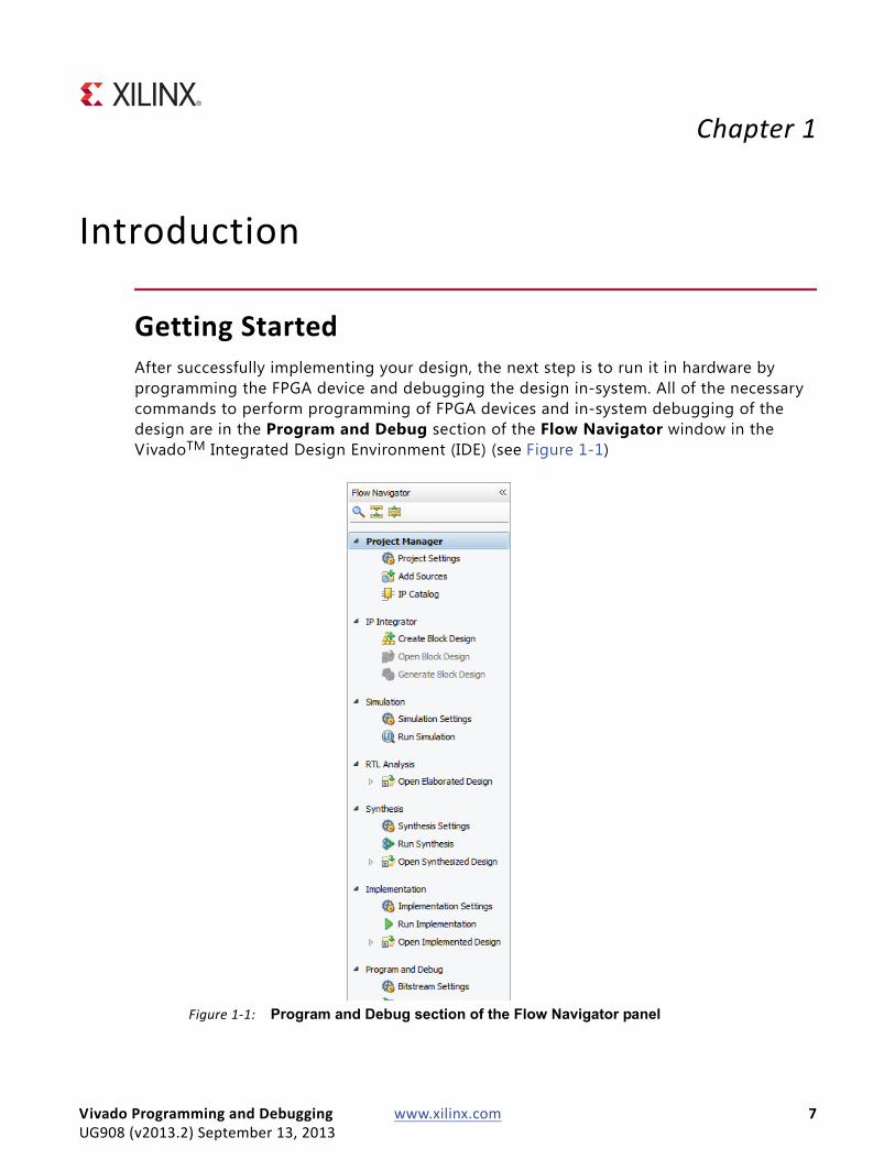
Getting StartedAfter successfully implementing your design, the next step is to run it in hardware by programming the FPGA device and debugging the design in-system. All of the necessary commands to perform programming of FPGA devices and in-system debugging of the design are in the Program and Debug section of the Flow Navigator window in the VivadoTM Integrated Design Environment (IDE) (see Figure 1-1)X-Ref Target - Figure 1-1
Figure 1-1: Program and Debug section of the Flow Navigator panel
Chapter 2
Programming the Device
IntroductionThe hardware programming phase is broken into two steps:
1. Generating the bitstream data programming f ile from the implemented design.
2. Connecting to hardware and downloading the programming file to the target FPGA device.
Generating the BitstreamBefore generating the bitstream data f ile, it is important to review the bitstream settings to make sure they are correct for your design.
There are two types of bitstream settings in Vivado™ IDE:
1. Bitstream file format settings.
2. Device configuration settings.
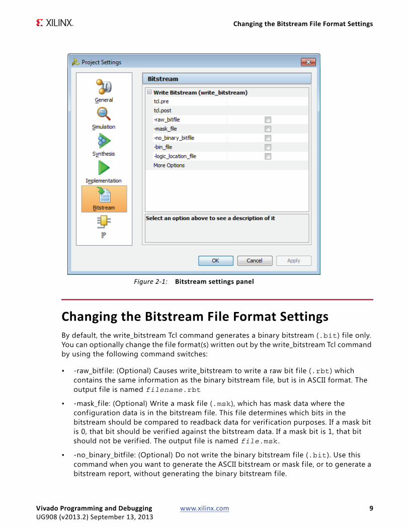
The Bitstream Settings button in the Flow Navigator and the Flow > Bitstream Settings menu selection opens the Bitstream section in the Project Settings popup window (see Figure 2-1). Once the bitstream settings are correct, the bitstream data f ile can be generated using the write_bistream Tcl command or by using the Generate Bitstream button in the Flow Navigator.
Vivado Programming and Debugging www.xilinx.com 8UG908 (v2013.2) September 13, 2013
Changing the Bitstream File Format Settings
Changing the Bitstream File Format SettingsBy default, the write_bitstream Tcl command generates a binary bitstream (.bit) f ile only. You can optionally change the f ile format(s) written out by the write_bitstream Tcl command by using the following command switches:
• -raw_bitf ile: (Optional) Causes write_bitstream to write a raw bit f ile (.rbt) which contains the same information as the binary bitstream file, but is in ASCII format. The output f ile is named filename.rbt
• -mask_file: (Optional) Write a mask f ile (.msk), which has mask data where the configuration data is in the bitstream file. This f ile determines which bits in the bitstream should be compared to readback data for verif ication purposes. If a mask bit is 0, that bit should be verif ied against the bitstream data. If a mask bit is 1, that bit should not be verif ied. The output file is named file.msk .
• -no_binary_bitfile: (Optional) Do not write the binary bitstream file (.bit). Use this command when you want to generate the ASCII bitstream or mask f ile, or to generate a bitstream report, without generating the binary bitstream file.
X-Ref Target - Figure 2-1
Figure 2-1: Bitstream settings panel
Vivado Programming and Debugging www.xilinx.com 9UG908 (v2013.2) September 13, 2013
Changing Device Configuration Bitstream Settings
• -logic_location_file: (Optional) Creates an ASCII logic location f ile (.ll) that shows the bitstream position of latches, flip-flops, LUTs, Block RAMs, and I/O block inputs and outputs. Bits are referenced by frame and bit number in the location f ile to help you observe the contents of FPGA registers.
• -bin_file: (Optional) Creates a binary f ile (.bin) containing only device programming data, without the header information found in the standard bitstream file (.bit).
• -reference_bitf ile <arg>: (Optional) Read a reference bitstream file, and output an incremental bitstream file containing only the differences from the specified reference f ile. This partial bitstream file can be used for incrementally programming an existing device with an updated design.
Changing Device Configuration Bitstream SettingsThe most common configuration settings that you can change fall into the device configuration settings category. These settings are properties on the device model and you change them by using the Properties window for the selected synthesized design netlist. The following steps describe how to set various bitstream properties using this method:
1. In the synthesized design, select the top-level design in the Netlist window.
2. In the Properties window, click the green “plus” sign to open the Add Properties dialog.
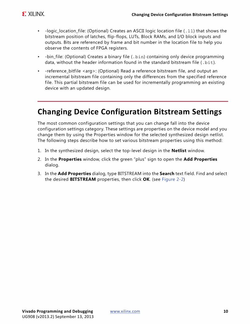
3. In the Add Properties dialog, type BITSTREAM into the Search text f ield. Find and select the desired BITSTREAM properties, then click OK. (see Figure 2-2)
Vivado Programming and Debugging www.xilinx.com 10UG908 (v2013.2) September 13, 2013
Changing Device Configuration Bitstream Settings
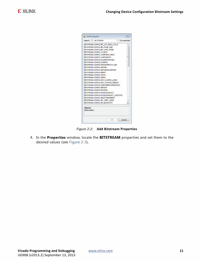
4. In the Properties window, locate the BITSTREAM properties and set them to the desired values (see Figure 2-3).
X-Ref Target - Figure 2-2
Figure 2-2: Add Bitstream Properties
Vivado Programming and Debugging www.xilinx.com 11UG908 (v2013.2) September 13, 2013
Programming the FPGA Device
You can also set the bitstream properties using the set_property command in an XDC file. For instance, here is an example on how to change the start-up DONE cycle property:
set_property BITSTREAM.STARTUP.DONE_CYCLE 4 [current_design]
Additional examples and templates are provided in the Vivado Templates. Appendix A, Device Configuration Bitstream Settings describes all of the device configuration settings.
Programming the FPGA DeviceThe next step after generating the bitstream data programming f ile is to download it into the target FPGA device. The Vivado tool offers two different ways to do this:
• Open a hardware session to use the native in-system device programming capabilities that are built into the Vivado IDE.
• Launch the iMPACT device programmer tool using the Launch iMPACT button in the Flow Navigator or Flow > Launch iMPACT menu option.
X-Ref Target - Figure 2-3
Figure 2-3: Netlist Bitstream Properties
Vivado Programming and Debugging www.xilinx.com 12UG908 (v2013.2) September 13, 2013
Using a Vivado Hardware Session to Program an FPGA Device
Using a Vivado Hardware Session to Program an FPGA DeviceThe Vivado IDE tool includes functionality that allows you to connect to hardware containing one or more FPGA devices to program and interact with those FPGA devices. Connecting to hardware can be done from either the Vivado IDE graphical user interface or by using Tcl commands. In either case, the steps to connect to hardware and program the target FPGA device are the same:
1. Open a hardware session.
2. Open a hardware target that is managed by a hardware server running on a host computer.
3. Associate the bitstream data programming f ile with the appropriate FPGA device.
4. Program or download the programming f ile into the hardware device.
Opening a Hardware SessionOpening a hardware session is the f irst step in programming and/or debugging your design in hardware. To open a hardware session, do one of the following:
• If you have a project open, click the Open Hardware Session button in the Program and Debug section of the Flow Navigator.
• Select the File > Open Hardware Session menu option.
• In the Tcl Console window, run the open_hw command
Opening Hardware Target ConnectionsThe next step in opening a hardware target (for instance, a hardware board containing a JTAG chain of one or more FPGA devices) is connecting to the hardware server (also called the Vivado CSE server or vcse_server application) that is managing the connection to the hardware target. You can do this one of three ways:
• Use the Open New Hardware Target selection in the Hardware view to use a wizard-based flow to open a new connection to a hardware target.
• Use the Open Recent Hardware Target selection in the Hardware view to re-open a connection to a previously connected hardware target.
• Use Tcl commands to open a connection to a hardware target.
Vivado Programming and Debugging www.xilinx.com 13UG908 (v2013.2) September 13, 2013
Using a Vivado Hardware Session to Program an FPGA Device
Connecting to Hardware Target Using hw_server TCF AgentVivado supports two methods of connecting to hardware targets:
• Using Target Communication Framework (TCF) Agent plug-ins [Default]
• Using legacy CSE plug-ins
The Xilinx TCF Agent is called Hardware Server (hw_server). The list of compatible JTAG download cables and devices that are supported by hw_server are:
• Xilinx Platform Cable USB II (DLC10)
• Xilinx Platform Cable USB (DLC9G, DLC9LP, DLC9)
• Digilent JTAG-HS2
• Digilent JTAG-SMT2
• Digilent JTAG-HS1
• Digilent JTAG-SMT1
The hw_server TCF agent is automatically started by vcse_server. However, you can also start the hw_server manually. For instance, on Windows platforms, at a cmd prompt run the following command:
C:\Xilinx\Vivado\vivado_release.version\bin\hw_server.bat
IMPORTANT: Vivado and vcse_server automatically try to connect to compatible JTAG targets using the hw_server TCF agent.
If you want to connect to JTAG targets using the legacy CSE plug-ins, follow these instructions:
• In Vivado: Before using the Open New Hardware Target wizard in the hardware session, run the following command:
set_param labtools.use_hw_server false
• If launching vcse_server manually, use the following command line to disable the launching of the hw_server TCF agent:
vcse_server -disable_tcf
Follow the steps in the next section to open a connection to a new hardware target using this agent.
Opening a New Hardware TargetThe Open New Hardware Target wizard provides an interactive way for you to connect to a hardware server and target. The wizard is a three-step process:
Vivado Programming and Debugging www.xilinx.com 14UG908 (v2013.2) September 13, 2013
Using a Vivado Hardware Session to Program an FPGA Device
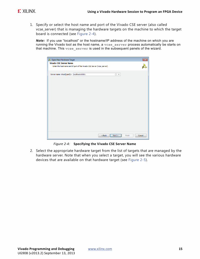
1. Specify or select the host name and port of the Vivado CSE server (also called vcse_server) that is managing the hardware targets on the machine to which the target board is connected (see Figure 2-4).
Note: If you use “localhost” or the hostname/IP address of the machine on which you are running the Vivado tool as the host name, a vcse_server process automatically be starts on that machine. This vcse_server is used in the subsequent panels of the wizard.
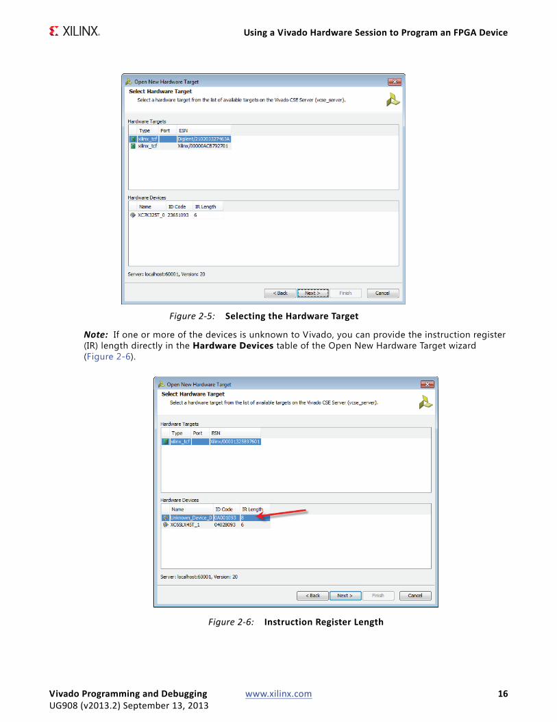
2. Select the appropriate hardware target from the list of targets that are managed by the hardware server. Note that when you select a target, you will see the various hardware devices that are available on that hardware target (see Figure 2-5).
X-Ref Target - Figure 2-4
Figure 2-4: Specifying the Vivado CSE Server Name
Vivado Programming and Debugging www.xilinx.com 15UG908 (v2013.2) September 13, 2013
Using a Vivado Hardware Session to Program an FPGA Device
Note: If one or more of the devices is unknown to Vivado, you can provide the instruction register (IR) length directly in the Hardware Devices table of the Open New Hardware Target wizard (Figure 2-6).
X-Ref Target - Figure 2-5
Figure 2-5: Selecting the Hardware Target
X-Ref Target - Figure 2-6
Figure 2-6: Instruction Register Length
Vivado Programming and Debugging www.xilinx.com 16UG908 (v2013.2) September 13, 2013
Using a Vivado Hardware Session to Program an FPGA Device
IMPORTANT: Vivado and vcse_server automatically try to connect to compatible JTAG targets using the hw_server TCF agent.
If you want to connect to JTAG targets using the legacy CSE plug-ins, follow these instructions:
• In Vivado: Before using the Open New Hardware Target wizard in the hardware session, run the following command:
set_param labtools.use_hw_server false
• If launching vcse_server manually, use the following command line to disable the launching of the hw_server TCF agent:
vcse_server -disable_tcf
3. Set the properties of the hardware target, such as the frequency of the TCK clock pin, etc. Note that each type of hardware target may have different properties. Refer to the documentation of each hardware target for more information about these properties.
Opening a Recent Hardware TargetThe Open New Hardware Target wizard is also what populates the list of previously connected hardware targets to be used by the Open Recent Hardware Target selection. Instead of connecting to a hardware target by going through the wizard, you can also re-open a connection to a previously connected hardware target by selecting the Open Recent Hardware Target link in the Hardware window and selecting one of the recently connected hardware server/target combinations in the list.
Opening a Hardware Target Using Tcl CommandsYou can also use Tcl commands to connect to a hardware server/target combination. For instance, to connect to the digilent_plugin target (serial number 210203339395) that is managed by the vcse_server running on localhost:60001, use the following Tcl commands:
connect_hw_server -host localhost -port 60001current_hw_target [get_hw_targets */xilinx_tcf/Digilent/210203327463A]open_hw_target
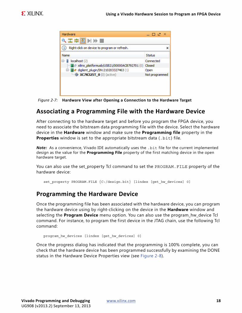
Once you finish opening a connection to a hardware target, the Hardware window is populated with the hardware server, hardware target, and various hardware devices for the open target (see Figure 2-7).
Vivado Programming and Debugging www.xilinx.com 17UG908 (v2013.2) September 13, 2013
Using a Vivado Hardware Session to Program an FPGA Device
Associating a Programming File with the Hardware DeviceAfter connecting to the hardware target and before you program the FPGA device, you need to associate the bitstream data programming f ile with the device. Select the hardware device in the Hardware window and make sure the Programming file property in the Properties window is set to the appropriate bitstream data (.bit) f ile.
Note: As a convenience, Vivado IDE automatically uses the .bit f ile for the current implemented design as the value for the Programming File property of the f irst matching device in the open hardware target.
You can also use the set_property Tcl command to set the PROGRAM.FILE property of the hardware device:
set_property PROGRAM.FILE {C:/design.bit} [lindex [get_hw_devices] 0]
Programming the Hardware DeviceOnce the programming f ile has been associated with the hardware device, you can program the hardware device using by right-clicking on the device in the Hardware window and selecting the Program Device menu option. You can also use the program_hw_device Tcl command. For instance, to program the f irst device in the JTAG chain, use the following Tcl command:
program_hw_devices [lindex [get_hw_devices] 0]
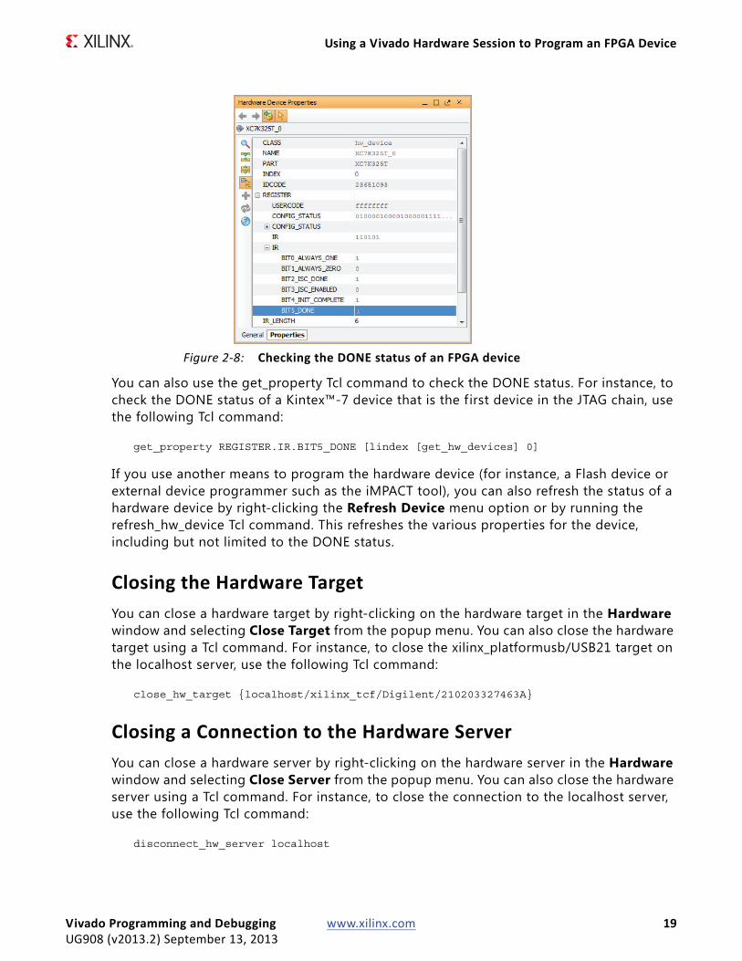
Once the progress dialog has indicated that the programming is 100% complete, you can check that the hardware device has been programmed successfully by examining the DONE status in the Hardware Device Properties view (see Figure 2-8).
X-Ref Target - Figure 2-7
Figure 2-7: Hardware View after Opening a Connection to the Hardware Target
Vivado Programming and Debugging www.xilinx.com 18UG908 (v2013.2) September 13, 2013
Using a Vivado Hardware Session to Program an FPGA Device
You can also use the get_property Tcl command to check the DONE status. For instance, to check the DONE status of a Kintex™-7 device that is the f irst device in the JTAG chain, use the following Tcl command:
get_property REGISTER.IR.BIT5_DONE [lindex [get_hw_devices] 0]
If you use another means to program the hardware device (for instance, a Flash device or external device programmer such as the iMPACT tool), you can also refresh the status of a hardware device by right-clicking the Refresh Device menu option or by running the refresh_hw_device Tcl command. This refreshes the various properties for the device, including but not limited to the DONE status.
Closing the Hardware TargetYou can close a hardware target by right-clicking on the hardware target in the Hardware window and selecting Close Target from the popup menu. You can also close the hardware target using a Tcl command. For instance, to close the xilinx_platformusb/USB21 target on the localhost server, use the following Tcl command:
close_hw_target {localhost/xilinx_tcf/Digilent/210203327463A}
Closing a Connection to the Hardware ServerYou can close a hardware server by right-clicking on the hardware server in the Hardware window and selecting Close Server from the popup menu. You can also close the hardware server using a Tcl command. For instance, to close the connection to the localhost server, use the following Tcl command:
disconnect_hw_server localhost
X-Ref Target - Figure 2-8
Figure 2-8: Checking the DONE status of an FPGA device
Vivado Programming and Debugging www.xilinx.com 19UG908 (v2013.2) September 13, 2013
Launching iMPACT
Launching iMPACTThe iMPACT tool lets you perform device configuration and file generation.
• Device Configuration lets you directly configure Xilinx® FPGAs and PROMs with the JTAG download cables (Xilinx Parallel Cable IV, Xilinx Platform Cable USB, Xilinx Platform Cable USB II, or Digilent JTAG cables).
• Operating in Boundary-Scan mode, iMPACT can configure or program Xilinx FPGAs, CPLDs, and PROMs.
• File generation enables you to create the following programming file types: System ACE™ CF, PROM, SVF, STAPL, and XSVF files.
iMPACT also lets you:
• Readback and verify design configuration data.
• Debug configuration problems.
• Execute SVF and XSVF f iles.
You can launch the iMPACT software tool directly from the Vivado IDE on any implemented design on which the Generate Bitstream command has been run. To invoke iMPACT, in the Flow Navigator, select Launch iMPACT.
The BIT bitstream file is passed automatically to iMPACT when launched from the Vivado tool. For more information on using iMPACT, see the iMPACT Help.
Vivado Programming and Debugging www.xilinx.com 20UG908 (v2013.2) September 13, 2013

Chapter 3
Debugging the Design
IntroductionDebugging an FPGA design is a multistep, iterative process. Like most complex problems, it is best to break the FPGA design debugging process down into smaller parts by focusing on getting smaller sections of the design working one at a time rather than trying to get the whole design to work at once. Iterating through the design flow by adding one module at a time and getting it to function properly in the context of the whole design is one example of a proven design and debug methodology. You can use this design and debug methodology in any combination of the following design flow stages:
• RTL-level design simulation
• Post-implemented design simulation
• In-system debugging
RTL-level Design SimulationThe design can be functionally debugged during the simulation verif ication process. Xilinx provides a full design simulation feature in the Vivado™ IDE. The Vivado design simulator can be used to perform RTL simulation of your design. The benefits of debugging your design in an RTL-level simulation environment include full visibility of the entire design and ability to quickly iterate through the design/debug cycle. The limitations of debugging your design using RTL-level simulation includes the diff iculty of simulating larger designs in a reasonable amount of time in addition to the diff iculty of accurately simulating the actual system environment. For more information about using the Vivado simulator, refer to the Vivado Design Suite User Guide: Logic Simulation (UG937) [Ref 1].
Vivado Programming and Debugging www.xilinx.com 21UG908 (v2013.2) September 13, 2013

Post-Implemented Design Simulation
Post-Implemented Design SimulationThe Vivado simulator can also be used to simulate the post-implemented design. One of the benefits of debugging the post-implemented design using the Vivado simulator includes having access to a timing-accurate model for the design. The limitations of performing post-implemented design simulation include those mentioned in the previous section: long run-times and system model accuracy.
In-System Logic Design DebuggingThe Vivado IDE also includes a logic analysis feature that enables you to perform in-system debugging of the post-implemented design an FPGA device. The benefits for debugging your design in-system include debugging your timing-accurate, post-implemented design in the actual system environment at system speeds. The limitations of in-system debugging includes somewhat lower visibility of debug signals compared to using simulation models and potentially longer design/implementation/debug iterations, depending on the size and complexity of the design.
In general, the Vivado tool provides several different ways to debug your design. You can use one or more of these methods to debug your design, depending on your needs. Chapter 4, In-System Logic Design Debugging Flows focuses on the in-system logic debugging capabilities of the Vivado IDE.
In-System Serial I/O Design DebuggingTo enable in-system serial I/O validation and debug, the Vivado IDE includes a serial I/O analysis feature. This allows you to measure and optimize your high-speed serial I/O links in your FPGA-based system. The Vivado serial I/O analyzer features are designed to help you address a range of in-system debug and validation problems from simple clocking and connectivity issues to complex margin analysis and channel optimization issues. The main benefit of using the Vivado serial I/O analyzer over some other external instrumentation techniques is that you are measuring the quality of the signal after the receiver equalization has been applied to the received signal. This ensures that you are measuring at the optimal point in the TX-to-RX channel thereby ensuring real and accurate data.
The Vivado tool provides the means to generate the design used to exercise the gigabit transceiver endpoints as well as the run-time software to take measurements and help you optimize your high-speed serial I/O channels. Chapter 7, In-System Serial I/O Debugging Flows guides you through the process of generating the IBERT design. Chapter 8, Debugging the Serial I/O Design in Hardware guides you through the use of the run-time Vivado serial I/O analyzer feature.
Vivado Programming and Debugging www.xilinx.com 22UG908 (v2013.2) September 13, 2013

Chapter 4
In-System Logic Design Debugging Flows
IntroductionThe Vivado tool provides many features to debug a design in-system in an actual hardware device. The in-system debugging flow has three distinct phases:
1. Probing phase: Identifying what signals in your design you want to probe and how you want to probe them.
2. Implementation phase: Implementing the design that includes the additional debug IP that is attached to the probed nets.
3. Analysis phase: Interacting with the debug IP contained in the design to debug and verify functional issues.
This in-system debug flow is designed to work using the iterative design/debug flow described in the previous section. If you choose to use the in-system debugging flow, it is advisable to get a part of your design working in hardware as early in the design cycle as possible. The rest of this chapter describes the three phases of the in-system debugging flow and how to use the Vivado™ logic debug feature to get your design working in hardware as quickly as possible.
Probing the Design for In-System DebuggingThe probing phase of the in-system debugging flow is split into two steps:
1. Identifying signals or nets that you want to probe
2. Deciding how you want to add debug core(s) to your design
In many cases, the decision you make on what signals to probe or how to probe them can affect one another. It helps to start by deciding if you want to manually add the debug IP component instances to your design source code (called the HDL instantiation probing flow) or if you want the Vivado tool to automatically insert the debug cores into your post-synthesis netlist (called the netlist insertion probing flow). Table 4-1 describes some of the advantages and trade-offs of the different debugging approaches.
Vivado Programming and Debugging www.xilinx.com 23UG908 (v2013.2) September 13, 2013
Using the Netlist Insertion Debug Probing Flow
Using the Netlist Insertion Debug Probing FlowInsertion of debug cores in the Vivado tool is presented in a layered approach to address different needs of the diverse group of Vivado users:
• The highest level is a simple wizard that creates and configures Integrated Logic Analyzer (ILA) v2.1 cores automatically based on the selected set of nets to debug.
• The next level is the main Debug window allowing control over individual debug cores, ports and their properties. The Debug window can be displayed by selecting the Debug layout from the Layout Selector or the Layout menu, or can be opened directly using Window > Debug.
• The lowest level is the set of Tcl debug commands that you can enter manually or replay as a script.
You can also use a combination of the modes to insert and customize debug cores.
Marking HDL Signals for DebugYou can identify signals for debugging at the HDL source level prior to synthesis by using the mark_debug constraint. Nets corresponding to signals marked for debug in HDL are automatically listed in the Debug window under the Unassigned Debug Nets folder in both the Debug Nets and Debug Cores.
Table 4-1: Debugging Strategies
Debugging Goal Recommended Debug Programming Flow
Identify debug signals in the HDL source code while retaining flexibility to enable/disable debugging later in the flow.
• Use mark_debug property to tag signals for debugging in HDL.• Use the Set up Debug wizard to guide you through the Netlist
Insertion probing flow.
Identify debug nets in synthesized design netlist without having to modify the HDL source code.
• Use the Mark Debug right-click menu option to select nets for debugging in the synthesized design netlist.
• Use the Set up Debug wizard to guide you through the Netlist Insertion probing flow.
Automated debug probing flow using Tcl commands.
• Use set_property Tcl command to set the mark_debug property on debug nets.
• Use Netlist Insertion probing flow Tcl commands to create debug core(s) and connect to them to debug nets.
Explicitly attach signals in the HDL source to an ILA debug core instance.
• Identify HDL signals for debugging.• Use the HDL Instantiation probing flow to generate and instantiate an
Integrated Logic Analyzer (ILA) core and connect it to the debug signals in the design.
Vivado Programming and Debugging www.xilinx.com 24UG908 (v2013.2) September 13, 2013
Using the Netlist Insertion Debug Probing Flow
Note: In the Debug window, the Debug Nets view is a more net-centric view of nets that you have selected for debug. The Debug Cores view is a more core-centric view where you can view and set core properties.
The procedure for marking nets for debug depends on whether you are working with an RTL source-based project or a synthesized netlist-based project. For an RTL netlist-based project:
• Using the Vivado synthesis feature you can optionally mark HDL signals for debug using the mark_debug constraint in VHDL and Verilog source f iles. The valid values for the mark_debug constraint are “TRUE” or “FALSE”. The Vivado synthesis feature does not support the “SOFT” value.
• Using Xilinx Synthesis Technology (XST) you can optionally mark nets for debug using the mark_debug constraint in VHDL and Verilog sources. In addition to the boolean string values of, “TRUE” or “FALSE,” a value of “SOFT” allows the software to optimize the specified net, if possible.
For a synthesized netlist-based project:
• Using the Synopsys® Synplify® synthesis tool, you can optionally mark nets for debug using the mark_debug and syn_keep constraints in VHDL or Verilog, or using the mark_debug constraint alone in the Synopsys Design Constraints (SDC) f ile. Synplify does not support the “SOFT” value, as this behavior is controlled by the syn_keep attribute.
• Using the Mentor Graphics® Precision® synthesis tool, you can optionally mark nets for debug using the mark_debug constraint in VHDL or Verilog.
The following subsections provide syntactical examples for Vivado synthesis, XST, Synplify, and Precision source files.
Vivado Synthesis mark_debug Syntax ExamplesThe following are examples of VHDL and Verilog syntax when using Vivado synthesis.
• VHDL Syntax Example
attribute mark_debug : string;attribute mark_debug of char_fifo_dout: signal is "true";
• Verilog Syntax Example
(* mark_debug = "true" *) wire [7:0] char_fifo_dout;
Vivado Programming and Debugging www.xilinx.com 25UG908 (v2013.2) September 13, 2013
Using the Netlist Insertion Debug Probing Flow
XST mark_debug Syntax ExamplesThe following are examples of VHDL and Verilog syntax when using XST.
• VHDL Syntax Example
attribute mark_debug : string;attribute mark_debug of char_fifo_dout: signal is "true";
• Verilog Syntax Example
(* mark_debug = "true" *) wire [7:0] char_fifo_dout;
Synplify mark_debug Syntax ExamplesThe following are examples of Synplify syntax for VHDL, Verilog, and SDC.
• VHDL Syntax Example
attribute syn_keep : boolean;attribute mark_debug : string;attribute syn_keep of char_fifo_dout: signal is true;attribute mark_debug of char_fifo_dout: signal is "true";
• Verilog Syntax Example
(* syn_keep = "true", mark_debug = "true" *) wire [7:0] char_fifo_dout;
• SDC Syntax Example
define_attribute {n:char_fifo_din[*]} {mark_debug} {"true"}
IMPORTANT: Net names in an SDC source must be prefixed with the “n:” qualifier.
Note: Synopsys Design Constraints (SDC) is an accepted industry standard for communicating design intent to tools, particularly for timing analysis. A reference copy of the SDC specif ication is available from Synopsys by registering for the TAP-in program at: http://www.synopsys.com/Community/Interoperability/Pages/TapinSDC.aspx
Precision mark_debug Syntax ExamplesThe following are examples of VHDL and Verilog syntax when using Precision.
• VHDL Syntax Example
attribute mark_debug : string;attribute mark_debug of char_fifo_dout: signal is "true";
• Verilog Syntax Example
(* mark_debug = "true" *) wire [7:0] char_fifo_dout;
Vivado Programming and Debugging www.xilinx.com 26UG908 (v2013.2) September 13, 2013
Using the Netlist Insertion Debug Probing Flow
Synthesizing the DesignThe next step is to synthesize the design containing the debug core(s) by clicking Run Synthesis in the Vivado IDE or by running the following Tcl commands:
launch_runs synth_1wait_on_run synth_1
You can also use the synth_design Tcl command to synthesize the design. Refer to the Vivado Design Suite User Guide: Synthesis (UG901) [Ref 2] for more details on the various ways you can synthesize your design.
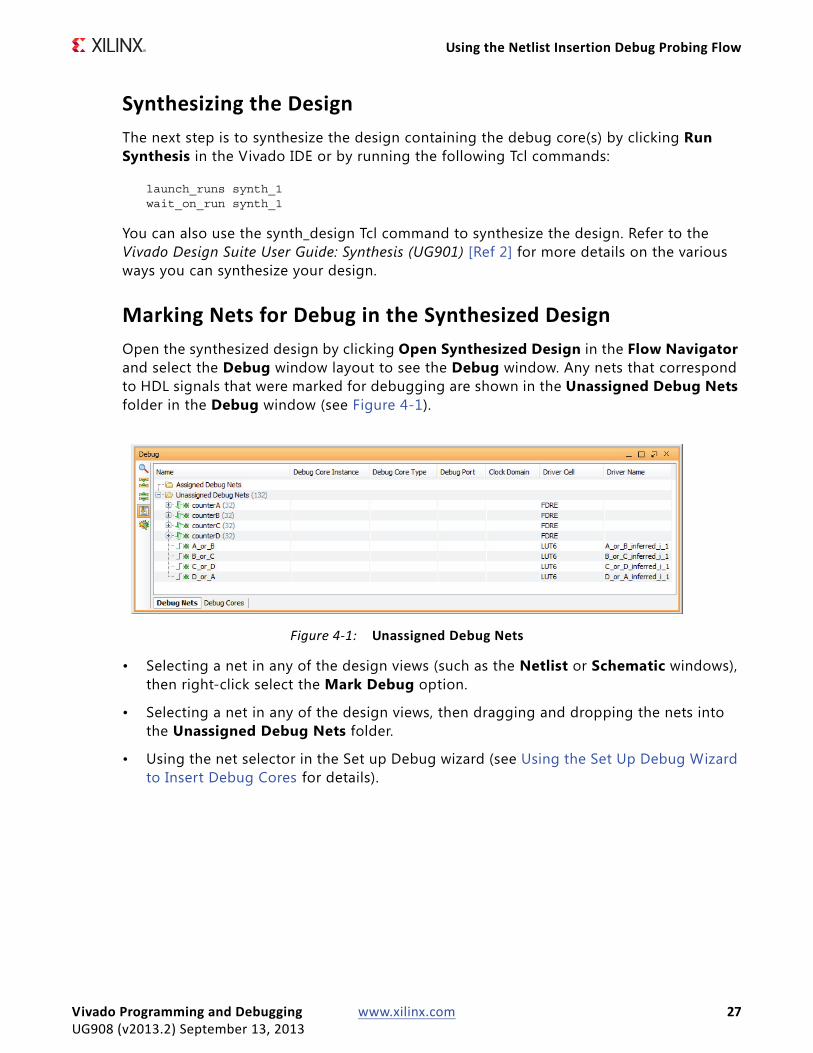
Marking Nets for Debug in the Synthesized DesignOpen the synthesized design by clicking Open Synthesized Design in the Flow Navigator and select the Debug window layout to see the Debug window. Any nets that correspond to HDL signals that were marked for debugging are shown in the Unassigned Debug Nets folder in the Debug window (see Figure 4-1).
• Selecting a net in any of the design views (such as the Netlist or Schematic windows), then right-click select the Mark Debug option.
• Selecting a net in any of the design views, then dragging and dropping the nets into the Unassigned Debug Nets folder.
• Using the net selector in the Set up Debug wizard (see Using the Set Up Debug Wizard to Insert Debug Cores for details).
X-Ref Target - Figure 4-1
Figure 4-1: Unassigned Debug Nets
Vivado Programming and Debugging www.xilinx.com 27UG908 (v2013.2) September 13, 2013
Using the Netlist Insertion Debug Probing Flow
Using the Set Up Debug Wizard to Insert Debug CoresThe next step after marking nets for debugging is to assign them to debug cores. The Vivado IDE provides an easy to use Set up Debug wizard to help guide you through the process of automatically creating the debug cores and assigning the debug nets to the inputs of the cores.
To use the Set up Debug wizard to insert the debug cores:
1. Optionally, select a set of nets for debugging either using the unassigned nets list or direct net selection.
2. Select Tools > Set up Debug from the Vivado IDE main menu.
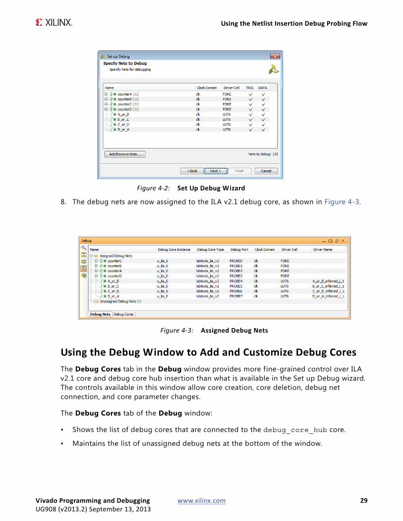
3. Click Next to get to the Specify Nets to Debug panel (see Figure 4-2).
4. Optionally, click Add/Remove Nets to add more nets or remove existing nets from the table.
5. Right-click a debug net and select Select Clock Domain to change the clock domain that will be used to sample value on the net.
Note: The Set up Debug wizard attempts to automatically select the appropriate clock domain for the debug net by searching the path for synchronous elements. Use the Select ClockDomain dialog window to modify this selection as needed, but be aware that each clock domain present in the table results in a separate ILA v2.1 core instance.
6. Once you are satisfied with the debug net selection, click Next.
Note: The Setup Debug wizard inserts one ILA core per clock domain. The nets that were selected for debug are assigned automatically to the probe ports of the inserted ILA v2.1 cores. The last wizard screen shows the core creation summary displaying the number of clocks found and ILA cores to be created and/or removed.
7. If you are satisf ied with the results, click Finish to insert and connect the ILA v2.1 cores in your synthesized design netlist.
Vivado Programming and Debugging www.xilinx.com 28UG908 (v2013.2) September 13, 2013
Using the Netlist Insertion Debug Probing Flow
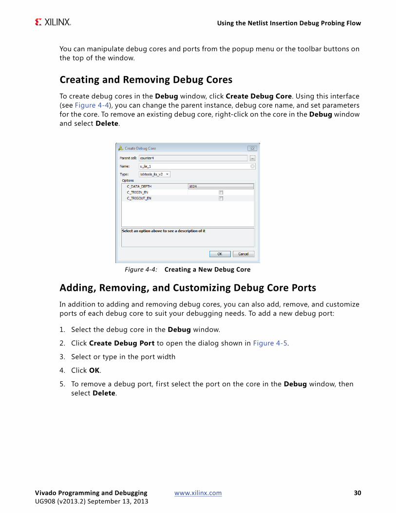
8. The debug nets are now assigned to the ILA v2.1 debug core, as shown in Figure 4-3.
Using the Debug Window to Add and Customize Debug CoresThe Debug Cores tab in the Debug window provides more fine-grained control over ILA v2.1 core and debug core hub insertion than what is available in the Set up Debug wizard. The controls available in this window allow core creation, core deletion, debug net connection, and core parameter changes.
The Debug Cores tab of the Debug window:
• Shows the list of debug cores that are connected to the debug_core_hub core.
• Maintains the list of unassigned debug nets at the bottom of the window.
X-Ref Target - Figure 4-2
Figure 4-2: Set Up Debug Wizard
X-Ref Target - Figure 4-3
Figure 4-3: Assigned Debug Nets
Vivado Programming and Debugging www.xilinx.com 29UG908 (v2013.2) September 13, 2013
Using the Netlist Insertion Debug Probing Flow
You can manipulate debug cores and ports from the popup menu or the toolbar buttons on the top of the window.
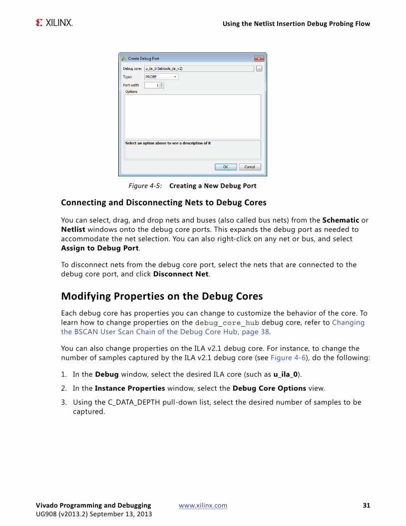
Creating and Removing Debug CoresTo create debug cores in the Debug window, click Create Debug Core. Using this interface (see Figure 4-4), you can change the parent instance, debug core name, and set parameters for the core. To remove an existing debug core, right-click on the core in the Debug window and select Delete.
Adding, Removing, and Customizing Debug Core PortsIn addition to adding and removing debug cores, you can also add, remove, and customize ports of each debug core to suit your debugging needs. To add a new debug port:
1. Select the debug core in the Debug window.
2. Click Create Debug Port to open the dialog shown in Figure 4-5.
3. Select or type in the port width
4. Click OK.
5. To remove a debug port, f irst select the port on the core in the Debug window, then select Delete.
X-Ref Target - Figure 4-4
Figure 4-4: Creating a New Debug Core
Vivado Programming and Debugging www.xilinx.com 30UG908 (v2013.2) September 13, 2013
Using the Netlist Insertion Debug Probing Flow
Connecting and Disconnecting Nets to Debug Cores
You can select, drag, and drop nets and buses (also called bus nets) from the Schematic or Netlist windows onto the debug core ports. This expands the debug port as needed to accommodate the net selection. You can also right-click on any net or bus, and select Assign to Debug Port.
To disconnect nets from the debug core port, select the nets that are connected to the debug core port, and click Disconnect Net.
Modifying Properties on the Debug CoresEach debug core has properties you can change to customize the behavior of the core. To learn how to change properties on the debug_core_hub debug core, refer to Changing the BSCAN User Scan Chain of the Debug Core Hub, page 38.
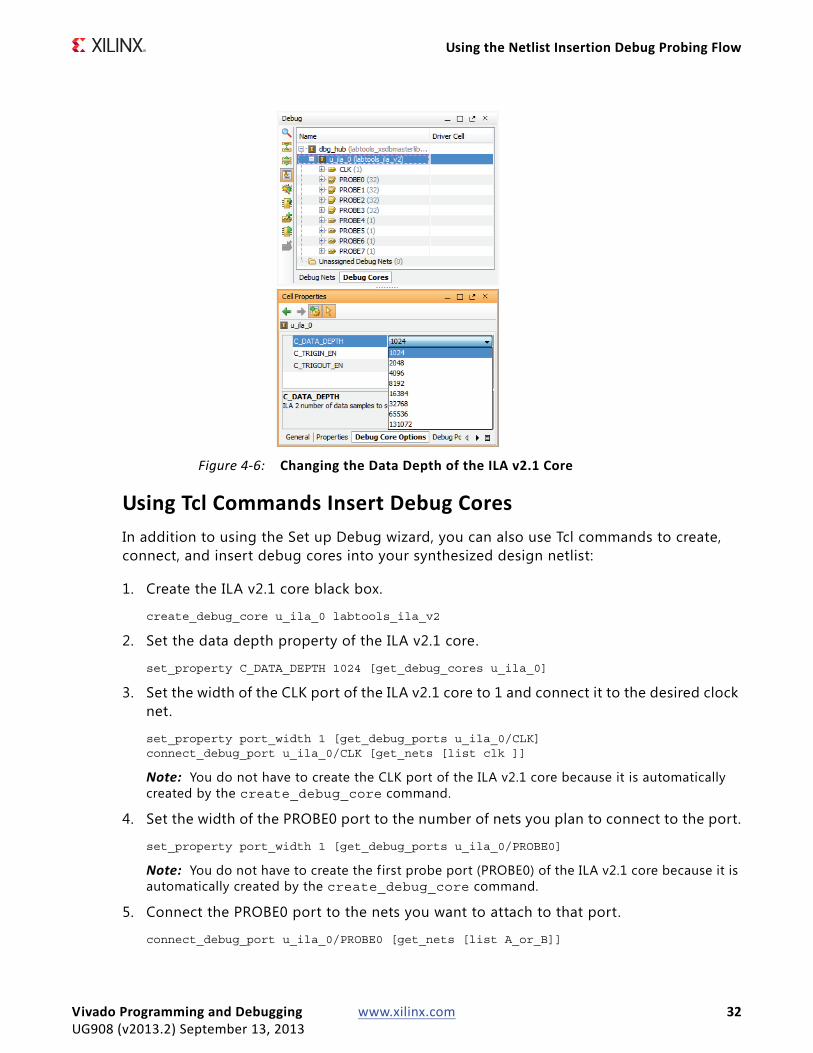
You can also change properties on the ILA v2.1 debug core. For instance, to change the number of samples captured by the ILA v2.1 debug core (see Figure 4-6), do the following:
1. In the Debug window, select the desired ILA core (such as u_ila_0).
2. In the Instance Properties window, select the Debug Core Options view.
3. Using the C_DATA_DEPTH pull-down list, select the desired number of samples to be captured.
X-Ref Target - Figure 4-5
Figure 4-5: Creating a New Debug Port
Vivado Programming and Debugging www.xilinx.com 31UG908 (v2013.2) September 13, 2013
Using the Netlist Insertion Debug Probing Flow
Using Tcl Commands Insert Debug CoresIn addition to using the Set up Debug wizard, you can also use Tcl commands to create, connect, and insert debug cores into your synthesized design netlist:
1. Create the ILA v2.1 core black box.
create_debug_core u_ila_0 labtools_ila_v2
2. Set the data depth property of the ILA v2.1 core.
set_property C_DATA_DEPTH 1024 [get_debug_cores u_ila_0]
3. Set the width of the CLK port of the ILA v2.1 core to 1 and connect it to the desired clock net.
set_property port_width 1 [get_debug_ports u_ila_0/CLK]connect_debug_port u_ila_0/CLK [get_nets [list clk ]]
Note: You do not have to create the CLK port of the ILA v2.1 core because it is automatically created by the create_debug_core command.
4. Set the width of the PROBE0 port to the number of nets you plan to connect to the port.
set_property port_width 1 [get_debug_ports u_ila_0/PROBE0]
Note: You do not have to create the f irst probe port (PROBE0) of the ILA v2.1 core because it is automatically created by the create_debug_core command.
5. Connect the PROBE0 port to the nets you want to attach to that port.
connect_debug_port u_ila_0/PROBE0 [get_nets [list A_or_B]]
X-Ref Target - Figure 4-6
Figure 4-6: Changing the Data Depth of the ILA v2.1 Core
Vivado Programming and Debugging www.xilinx.com 32UG908 (v2013.2) September 13, 2013
HDL Instantiation Debug Probing Flow Overview
6. Optionally, create more probe ports, set their width, and connect them to the nets you want to debug.
create_debug_port u_ila_0 PROBEset_property port_width 2 [get_debug_ports u_ila_0/PROBE1]connect_debug_port u_ila_0/PROBE1 [get_nets [list {A[0]} {A[1]}]]
7. Optionally, generate and synthesize the debug core(s) so you can floorplan them with the rest of your synthesized design.
implement_debug_core [get_debug_cores]
For more information on these and other related Tcl commands, type help –category ChipScope in the Tcl Console of the Vivado IDE.
Implementing the DesignAfter inserting, connecting and customizing your debug cores, you are now ready for implementing your design (refer to the section called Implementing the Design Containing the Debug Cores).
HDL Instantiation Debug Probing Flow OverviewThe HDL instantiation probing flow involves the manual customization, instantiation, and connection of various debug core components directly in the HDL design source. The new debug cores that are supported in this flow in the Vivado tool are shown in table Table 4-2. The legacy debug cores that are supported in this flow in the Vivado tool are shown in Table 4-3.
Table 4-2: Debug Cores in Vivado IP Catalog available for use in the HDL Instantiation Probing Flow
Debug Core Version Description Run-time Analyzer Tool
ILA (Integrated Logic Analyzer)
v2.1 Debug core that is used totrigger on hardware eventsand capture data at systemspeeds.
Vivado logic analyzer
VIO (Virtual Input/Output)
v2.0 Debug core that is used tomonitor or control signals ina design at JTAG chain scanrates.
Vivado logic analyzer
Vivado Programming and Debugging www.xilinx.com 33UG908 (v2013.2) September 13, 2013
HDL Instantiation Debug Probing Flow Overview
The ICON, VIO, and ILA v1.x cores are supported in the Vivado tool flow to provide compatibility with legacy designs that contain these cores.
However, these cores are not available in the Vivado IP Catalog. You must supply the legacy debug cores netlist (.ngc) f ile, synthesis (.v or .vhd) template f ile, and constraints (.xdc) f ile that were previously generated using the Xilinx ISE CORE Generator as source f iles in your Vivado project. You must also set properties on these f iles to make sure they work properly in the Vivado tool flow. Here is an example of how to add legacy ICON, ILA, and VIO files to your Vivado project:
• Add the .ngc and .v f iles.
add_files -norecurse {./icon_v1_06a.ngc} add_files -norecurse {./ila_v1_05a.ngc} add_files -norecurse {./vio_v1_05a.ngc} add_files -norecurse {./icon_v1_06a.v} add_files -norecurse {./ila_v1_05a.v} add_files -norecurse {./vio_v1_05a.v}
• Import the .xdc f iles and specify that they are not used during synthesis.
import_files -fileset constrs_1 -force -norecurse {./icon_v1_06a.xdc} import_files -fileset constrs_1 -force -norecurse {./ila_v1_05a.xdc} import_files -fileset constrs_1 -force -norecurse {./vio_v1_05a.xdc} set_property used_in_synthesis false [get_files icon_v1_06a.xdc] set_property used_in_synthesis false [get_files vio_v1_05a.xdc] set_property used_in_synthesis false [get_files ila_v1_05a.xdc]
• Scope the legacy ILA core's .xdc f ile to the cell reference for the ILA core module.
set_property SCOPED_TO_REF {ila_v1_05a} [get_files ila_v1_05a.xdc]
Table 4-3: Legacy ChipScope Pro Debug Cores available for use in the HDL Instantiation Probing Flow
Debug Core Version Description Run-time Analyzer Tool
ICON (Integrated Controller)
v1.06a Debug core hub used to connect the ILA 1.05a and VIO 1.05a cores to the JTAG chain.
ChipScope Pro Analyzer
VIO (Virtual Input/Output)
v1.05a Debug core that is used to monitor or control signals in a design at JTAG chain scan rates. Requires connection to an ICON core.
ChipScope Pro Analyzer
ILA (Integrated Logic Analyzer)
v1.05a Debug core that is used to trigger on hardware events and capture data at system speeds. Requires connection to an ICON core.
ChipScope Pro Analyzer
ILA (Integrated Logic Analyzer)
v2.0 Debug core that is used to trigger on hardware events and capture data at system speeds.
Vivado logic analyzer
Vivado Programming and Debugging www.xilinx.com 34UG908 (v2013.2) September 13, 2013
Using the HDL Instantiation Debug Probing Flow
The new ILA v2.1 core has two distinct advantages over the legacy ILA v1.x core:
• Works with the integrated Vivado logic analyzer feature (refer to Debugging Logic Designs in Hardware, page 40).
• No ICON core instance or connection is required.
Using the HDL Instantiation Debug Probing FlowThe steps required to perform the HDL instantiation flow are:
1. Customize and generate the ILA v2.1 debug core(s) that have the right number of probe ports for the signals you want to probe.
2. Synthesize the design containing the debug core(s).
3. (Optional) Modify debug core properties.
4. Implement the design containing the debug core(s).
Customizing and Generating the Debug CoresUse the IP Catalog button in the Project Manager to locate, select, and customize the desired debug core. The debug cores are located in the Debug & Verification > Debug category of the IP Catalog (see Figure 4-7). You can customize the debug core by double-clicking on the IP core or by right-click selecting the Customize IP menu selection.
• For more information on customizing the ILA v2.1 core, please refer to LogiCORE IP Integrated Logic Analyzer (ILA) (v2.0) Datasheet (DS875) [Ref 7].
• For more information on customizing the VIO v2.0 core, please refer to LogiCORE IP Virtual Input/Output (VIO) v2.0 Product Guide (PG159) [Ref 8].
Vivado Programming and Debugging www.xilinx.com 35UG908 (v2013.2) September 13, 2013

Using the HDL Instantiation Debug Probing Flow
After customizing the core, click the Generate button in the IP customization wizard. This generates the customized debug core and add it to the Sources view of your project.
Instantiating the Debug CoresAfter generating the debug core, instantiate it in your HDL source code and connect it to the signals that you wish to probe for debugging purposes. Below is an example of the ILA v2.1 instance in a Verilog HDL source file:
ila_v2_1_0 i_ila ( .CLK(clk), .PROBE0(counterA), .PROBE1(counterB), .PROBE2(counterC), .PROBE3(counterD), .PROBE4(A_or_B), .PROBE5(B_or_C), .PROBE6(C_or_D), .PROBE7(D_or_A));
Note: Unlike the legacy VIO and ILA v1.x cores, the ILA v2.1 core instance does not require a connection to an ICON core instance. Instead, a debug_core_hub debug core is automatically inserted into the synthesized design netlist to provide connectivity between the ILA v2.1 core and the JTAG scan chain.
X-Ref Target - Figure 4-7
Figure 4-7: Debug Cores in the IP Catalog
Vivado Programming and Debugging www.xilinx.com 36UG908 (v2013.2) September 13, 2013
Using the HDL Instantiation Debug Probing Flow
Synthesizing the Design Containing the Debug CoresIn the next step, synthesize the design containing the debug core(s) by clicking Run Synthesis in the Vivado IDE or by running the following Tcl commands:
launch_runs synth_1wait_on_run synth_1
You can also use the synth_design Tcl command to synthesize the design. Refer to Vivado Design Suite User Guide: Synthesis (UG901) [Ref 2] for more details on the various ways you can synthesize your design.
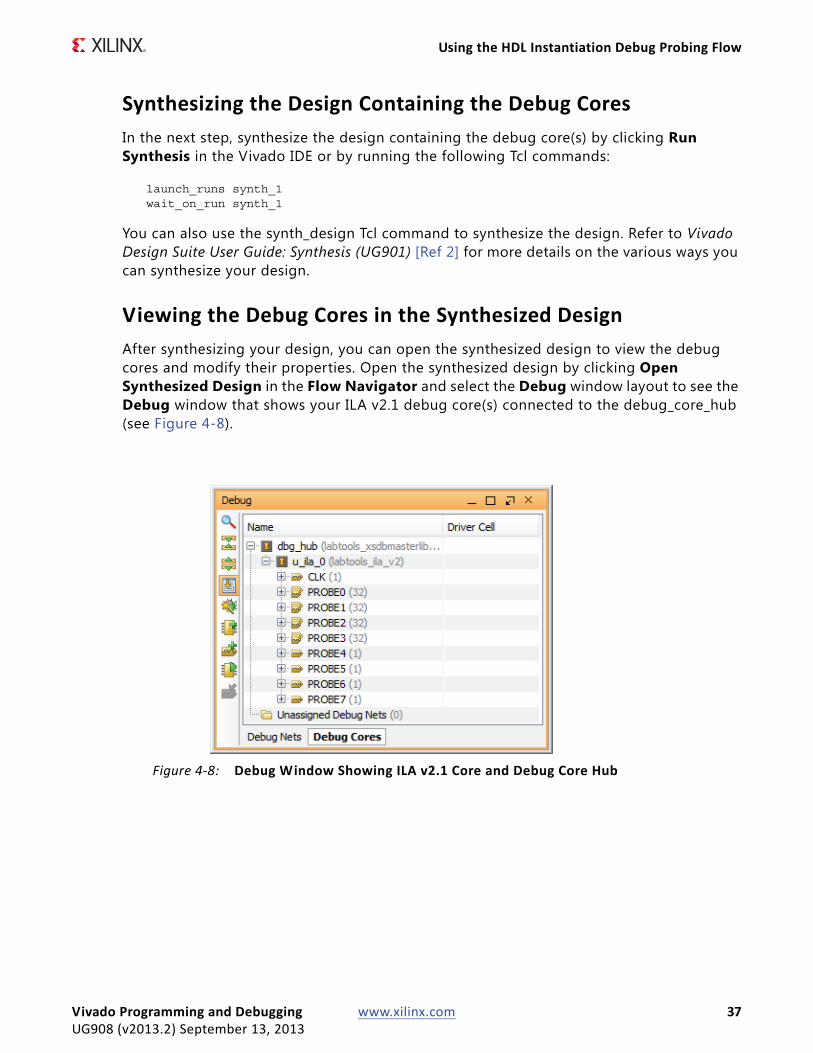
Viewing the Debug Cores in the Synthesized DesignAfter synthesizing your design, you can open the synthesized design to view the debug cores and modify their properties. Open the synthesized design by clicking Open Synthesized Design in the Flow Navigator and select the Debug window layout to see the Debug window that shows your ILA v2.1 debug core(s) connected to the debug_core_hub (see Figure 4-8).
X-Ref Target - Figure 4-8
Figure 4-8: Debug Window Showing ILA v2.1 Core and Debug Core Hub
Vivado Programming and Debugging www.xilinx.com 37UG908 (v2013.2) September 13, 2013
Using the HDL Instantiation Debug Probing Flow
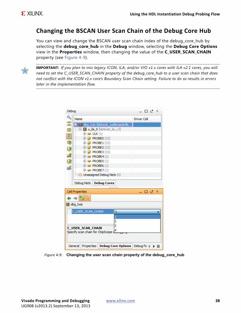
Changing the BSCAN User Scan Chain of the Debug Core HubYou can view and change the BSCAN user scan chain index of the debug_core_hub by selecting the debug_core_hub in the Debug window, selecting the Debug Core Options view in the Properties window, then changing the value of the C_USER_SCAN_CHAIN property (see Figure 4-9).
IMPORTANT: If you plan to mix legacy ICON, ILA, and/or VIO v1.x cores with ILA v2.1 cores, you will need to set the C_USER_SCAN_CHAIN property of the debug_core_hub to a user scan chain that does not conflict with the ICON v1.x core’s Boundary Scan Chain setting. Failure to do so results in errors later in the implementation flow.
X-Ref Target - Figure 4-9
Figure 4-9: Changing the user scan chain property of the debug_core_hub
Vivado Programming and Debugging www.xilinx.com 38UG908 (v2013.2) September 13, 2013
Implementing the Design Containing the Debug Cores
Implementing the Design Containing the Debug CoresThe Vivado software creates the debug_core_hub debug cores initially as black boxes. These cores must be implemented prior to running the placer and router.
Implementing the Debug Cores
Debug core implementation is done automatically when implementing the design; however, you can also force debug core implementation manually for floorplanning or timing analysis. To manually implement the cores: do one of the following:
• Click the Implement Debug Cores icon on the toolbar menu of the Debug window.
• Right-click on any debug core in the Debug window and select the Implement Debug Cores option from the popup menu.
The Vivado IDE generates and synthesizes each black box debug core. This operation can take some time. A progress indicator shows that the operation is running. When the debug core implementation is complete, the debug core black boxes are resolved and you can access the generated instances.
Implementing the DesignImplement the design containing the debug core(s) by clicking Run Implementation in the Vivado IDE or by running the following Tcl commands:
launch_runs impl_1wait_on_run impl_1
You can also implement the design using the implementation commands opt_design, place_design, and route_design. Refer to the Vivado Design Suite User Guide: Implementation (UG904) [Ref 3] for more details on the various ways you can implement your design.
Vivado Programming and Debugging www.xilinx.com 39UG908 (v2013.2) September 13, 2013
Chapter 5
Debugging Logic Designs in Hardware
IntroductionOnce you have the debug core(s) in your design, you can use the run-time logic analyzer features to debug the design in hardware. Two different tools can be used depending on the type of debug cores in your design:
• ChipScope™ Pro Analyzer: used with ICON v1.x, ILA v1.x, VIO v1.x, and IBERT v2.x debug cores.
• Vivado™ logic analyzer feature: used with ILA v2.1, VIO v2.0, and IBERT v3.x debug cores.
If you have a mixture of ICON/ILA/VIO v1.x and ILA/VIO v2.x debug cores in your design, you can simultaneously use both the ChipScope Pro Analyzer tool and Vivado logic analyzer feature to debug the same design running on the same hardware target board (see section called Using Vivado Logic Analyzer to Debug the Design, page 41 for more details).
Launching ChipScope Pro Analyzer to Debug the DesignThe ChipScope Pro Analyzer tool is used to interact with ICON v1.x, ILA v1.x, and VIO v1.x debug cores that are in your design. When the ChipScope Pro Analyzer software is installed, you can launch it directly from the Vivado IDE on any implemented design on which Generate Bitstream has been run.
IMPORTANT: The ChipScope Pro and iMPACT tools are not included in the Vivado Design Suite installation. However, these tools are available in an installation package called the ISE Design Suite: Standalone Lab Tools that is freely downloadable from the Xilinx Download site at http://www.xilinx.com/downloads.
Vivado Programming and Debugging www.xilinx.com 40UG908 (v2013.2) September 13, 2013
Using Vivado Logic Analyzer to Debug the Design
To launch ChipScope Pro Analyzer, do one of the following:
• Use the Flow > Launch ChipScope Analyzer command from the main menu
• Run the launch_chipscope_analyzer Tcl command in the Tcl Console
The Vivado IDE passes the BIT bitstream and CDC net connection name files automatically to the ChipScope Pro Analyzer tool. For more information about ChipScope Pro Analyzer see the Xilinx website,http: http://www.xilinx.com/support/index.html/content/xilinx/en/supportNav/design_tools/chipscope_pro.html
Using Vivado Logic Analyzer to Debug the DesignThe Vivado logic analyzer feature is used to interact with ILA v2.1 debug cores that are in your design. To access the Vivado logic analyzer feature, click the Open Hardware Session button in the Program and Debug section of the Flow Navigator.
The steps to debug your design in hardware are:
1. Connect to the hardware target and program the FPGA device with the .bit f ile
2. Set up the ILA debug core trigger and probe compare conditions.
3. Arm the ILA debug core trigger.
4. View the captured data from the ILA debug core in the Waveform window.
Connecting to the Hardware Target and Programming the FPGA DeviceProgramming an FPGA device prior to debugging are exactly the same steps described in Using a Vivado Hardware Session to Program an FPGA Device in Chapter 2 . After programming the device with the .bit f ile that contains the ILA v2.1 and VIO v2.0 cores, the Hardware window now shows the ILA and VIO cores that were detected when scanning
Vivado Programming and Debugging www.xilinx.com 41UG908 (v2013.2) September 13, 2013
Setting up the ILA Core to Take a Measurement
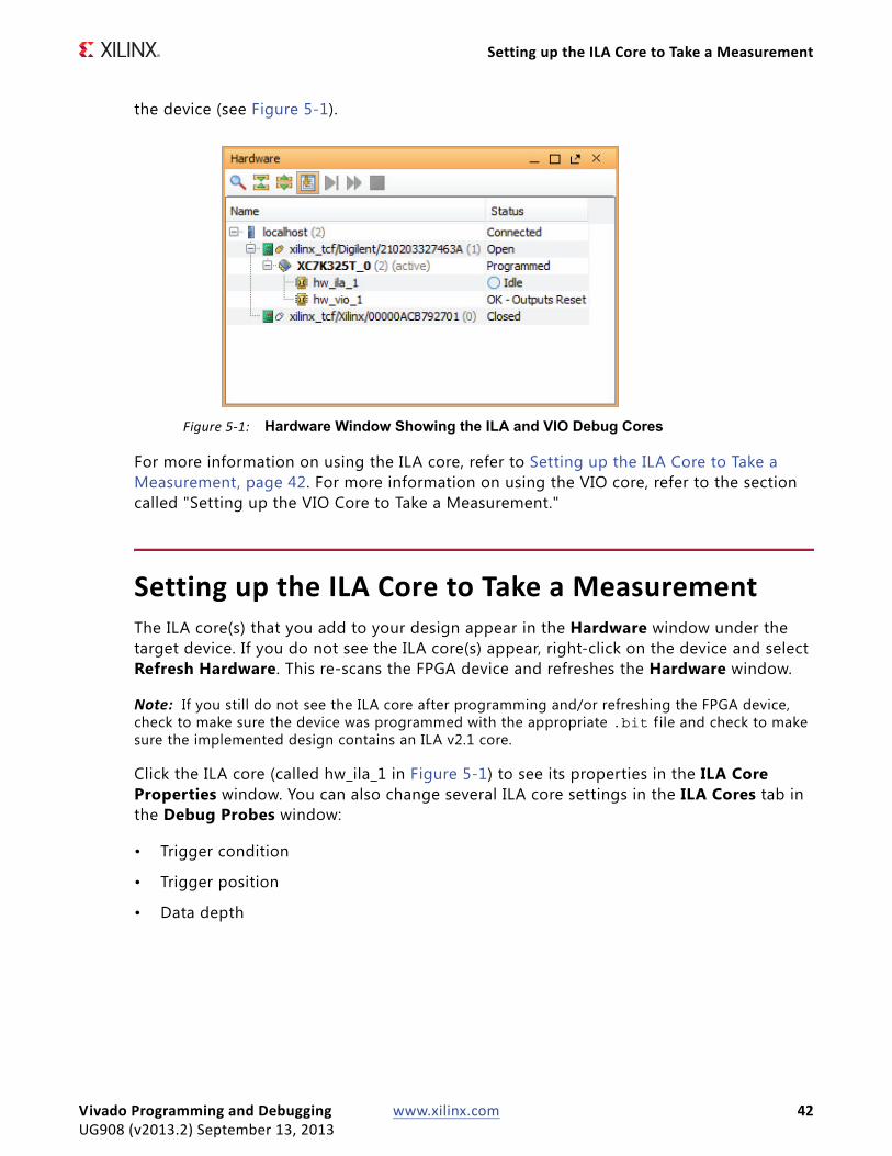
the device (see Figure 5-1).
For more information on using the ILA core, refer to Setting up the ILA Core to Take a Measurement, page 42. For more information on using the VIO core, refer to the section called "Setting up the VIO Core to Take a Measurement."
Setting up the ILA Core to Take a MeasurementThe ILA core(s) that you add to your design appear in the Hardware window under the target device. If you do not see the ILA core(s) appear, right-click on the device and select Refresh Hardware. This re-scans the FPGA device and refreshes the Hardware window.
Note: If you still do not see the ILA core after programming and/or refreshing the FPGA device, check to make sure the device was programmed with the appropriate .bit f ile and check to make sure the implemented design contains an ILA v2.1 core.
Click the ILA core (called hw_ila_1 in Figure 5-1) to see its properties in the ILA Core Properties window. You can also change several ILA core settings in the ILA Cores tab in the Debug Probes window:
• Trigger condition
• Trigger position
• Data depth
X-Ref Target - Figure 5-1
Figure 5-1: Hardware Window Showing the ILA and VIO Debug Cores
Vivado Programming and Debugging www.xilinx.com 42UG908 (v2013.2) September 13, 2013
Setting the ILA Core Trigger Condition
Setting the ILA Core Trigger ConditionUse the Trigger Cond control in the ILA Cores tab in the Debug Probes window (or the Trigger Condition property in the ILA Core Properties window) to select between “AND” and “OR” settings. The “AND” setting causes a trigger event when all of the ILA probe comparisons are satisfied. The “OR” setting causes a trigger event when any of the ILA probe comparisons are satisf ied. You can also use the set_property Tcl command to change the ILA core trigger condition:
set_property CONTROL.TRIGGER_CONDITION AND [get_hw_ilas hw_ila_1]
Setting the ILA Core Trigger PositionUse the Trigger Pos control in the ILA Cores tab in the Debug Probes window (or the Trigger Position property in the ILA Core Properties window) to set the position of the trigger mark in the captured data buffer. You can set the trigger position to any sample number in the captured data buffer. For instance, in the case of a captured data buffer that is 1024 samples deep:
• Sample number 0 corresponds to the f irst (left-most) sample in the captured data buffer.
• Sample number 1023 corresponds to the last (right-most) sample in the captured data buffer.
• Samples numbers 511 and 512 correspond to the two “center” samples in the captured data buffer.
You can also use the set_property Tcl command to change the ILA core trigger position:
set_property CONTROL.TRIGGER_POSITION 512 [get_hw_ilas hw_ila_1]
Setting the ILA Core Data DepthUse the Data Depth control in the ILA Cores tab in the Debug Probes window (or the Capture data depth property in the ILA Core Properties window) to set the data depth of the ILA core captured data buffer. You can set the data depth to any power of two from 1 to the maximum data depth.
Note: Refer to the section called Modifying Properties on the Debug Cores, page 31 for more details on how to set the maximum capture buffer data depth on ILA cores that are added to the design using the Netlist Insertion probing flow.
You can also use the set_property Tcl command to change the ILA core data depth:
set_property CONTROL.DATA_DEPTH 512 [get_hw_ilas hw_ila_1]
Vivado Programming and Debugging www.xilinx.com 43UG908 (v2013.2) September 13, 2013
Writing ILA Probes Information
Writing ILA Probes InformationThe ILA Cores tab view in the Debug Probes window contains information about the nets that you probed in your design using the ILA v2.1 core. This ILA probe information is extracted from your design and is stored in a data file that typically has an .ltx f ile extension.
Normally, the ILA probe file is automatically created during the implementation process. However, you can also use the write_debug_probes Tcl command to write out the debug probes information to a f ile:
1. Open the Synthesized or Netlist Design.
2. Run the write_debug_probes filename.ltx Tcl command.
Reading ILA Probes InformationThe ILA probe f ile is automatically associated with the FPGA hardware device if the probes f ile is called debug_nets.ltx and is found in the same directory as the bitstream programming (.bit) f ile that is associated with the device.
You can also specify the location of the probes f ile:
1. Select the FPGA device in the Hardware window.
2. Set the Probes file location in the Hardware Device Properties window.
3. Click Apply to apply the change.
You can also set the location using the set_property Tcl command:
set_property PROBES.FILE {C:/myprobes.ltx} [lindex [get_hw_devices] 0]
Viewing ILA ProbesThe ILA Cores tab in the Debug Probes window is used to view the probes associated with each ILA core. Once the probes f ile is associated with the FPGA hardware device, select the hardware device and use the right-click Refresh Device command to refresh the ILA Cores
Vivado Programming and Debugging www.xilinx.com 44UG908 (v2013.2) September 13, 2013
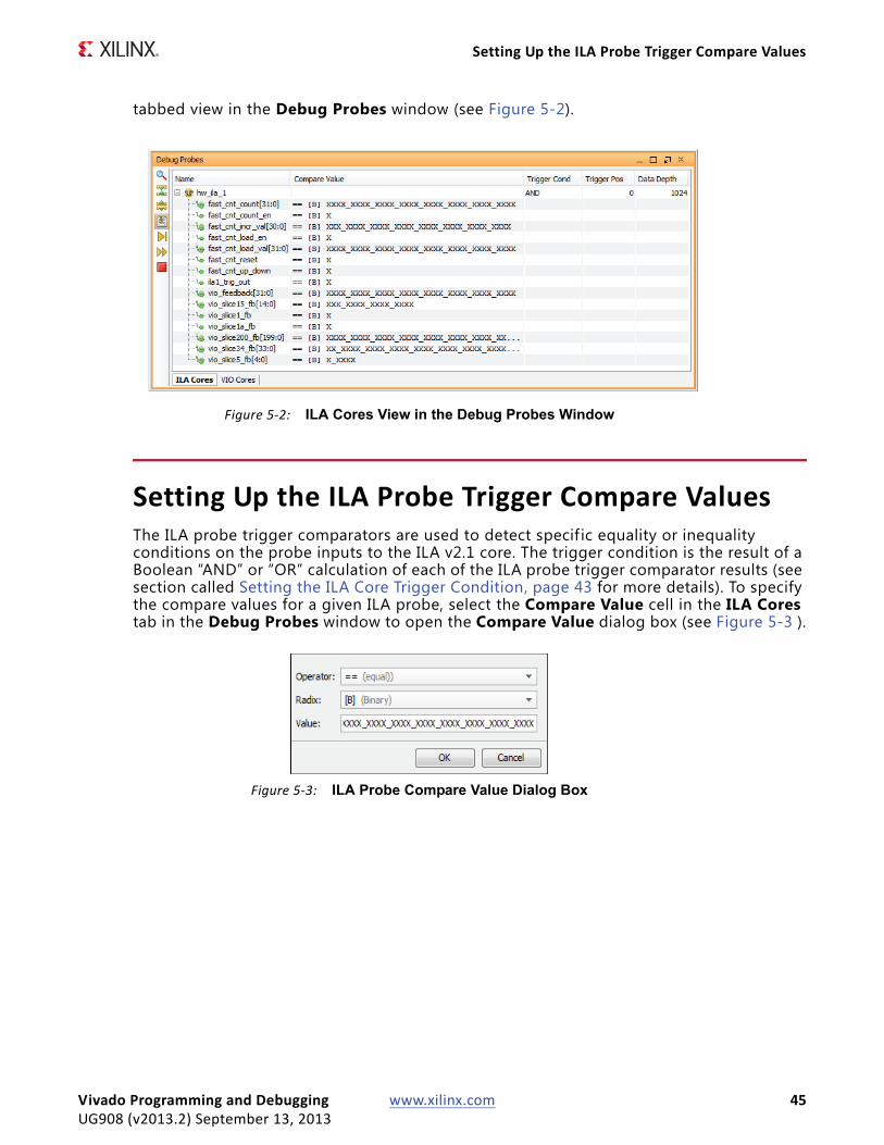
Setting Up the ILA Probe Trigger Compare Values
tabbed view in the Debug Probes window (see Figure 5-2).
Setting Up the ILA Probe Trigger Compare ValuesThe ILA probe trigger comparators are used to detect specif ic equality or inequality conditions on the probe inputs to the ILA v2.1 core. The trigger condition is the result of a Boolean “AND” or “OR” calculation of each of the ILA probe trigger comparator results (see section called Setting the ILA Core Trigger Condition, page 43 for more details). To specify the compare values for a given ILA probe, select the Compare Value cell in the ILA Cores tab in the Debug Probes window to open the Compare Value dialog box (see Figure 5-3 ).
X-Ref Target - Figure 5-2
Figure 5-2: ILA Cores View in the Debug Probes Window
X-Ref Target - Figure 5-3
Figure 5-3: ILA Probe Compare Value Dialog Box
Vivado Programming and Debugging www.xilinx.com 45UG908 (v2013.2) September 13, 2013
ILA Probe Compare Value Settings
ILA Probe Compare Value SettingsThe Compare Value dialog box contains three fields that you can configure:
1. Operator : This is the comparison operator that you can set to the following values:
° == (equal)
° != (not equal)
° < (less than)
° <= (less than or equal)
° > (greater than)
° >= (greater than or equal)
2. Radix: This is the radix or base of the Value that you can set to the following values:
° [B] Binary
° [H] Hexadecimal
° [O] Octal
° [A] ASCII
° [U] Unsigned Decimal
° [S] Signed Decimal
3. Value: This is the comparison value that will be compared (using the Operator) with the real-time value on the net(s) in the design that are connected to the probe input of the ILA v2.1 debug core. Depending on the Radix settings, the Value string is as follows:
° Binary
- 0: logical zero
- 1: logical one
- X: don’t care
- R: rising or low-to-high transition
- F: falling or high-to-low transition
- B: either low-to-high or high-to-low transitions
- N: no transition (current sample value is the same as the previous value)
Vivado Programming and Debugging www.xilinx.com 46UG908 (v2013.2) September 13, 2013

Running or Arming the ILA Core Trigger
° Hexadecimal
- X: All bits corresponding to the value string character are “don’t care” values
- 0-9: Values 0 through 9
- A-F: Values 10 through 15
° Octal
- X: All bits corresponding to the value string character are “don’t care” values
- 0-7: Values 0 through 7
° ASCII
- Any string made up of ASCII characters
° Unsigned Decimal
- Any non-negative integer value
° Signed Decimal
- Any integer value
Running or Arming the ILA Core TriggerYou can run or arm the ILA core trigger in two different modes:
• Run Trigger : Selecting the ILA core to be armed followed by clicking the Run Trigger button on the Hardware or Debug Probes window toolbar arms the ILA core to detect the trigger event that is defined by the ILA core trigger condition and probe compare values.
• Run Trigger Immediate: Selecting the ILA core to be armed followed by clicking the Run Trigger Immediate button on the Hardware or Debug Probes window toolbar arms the ILA core to trigger immediately regardless of the settings of the ILA core trigger condition and probe compare values. This command is useful for capturing any values that present at the probe inputs of the ILA core.
Vivado Programming and Debugging www.xilinx.com 47UG908 (v2013.2) September 13, 2013
Stopping the ILA Core Trigger
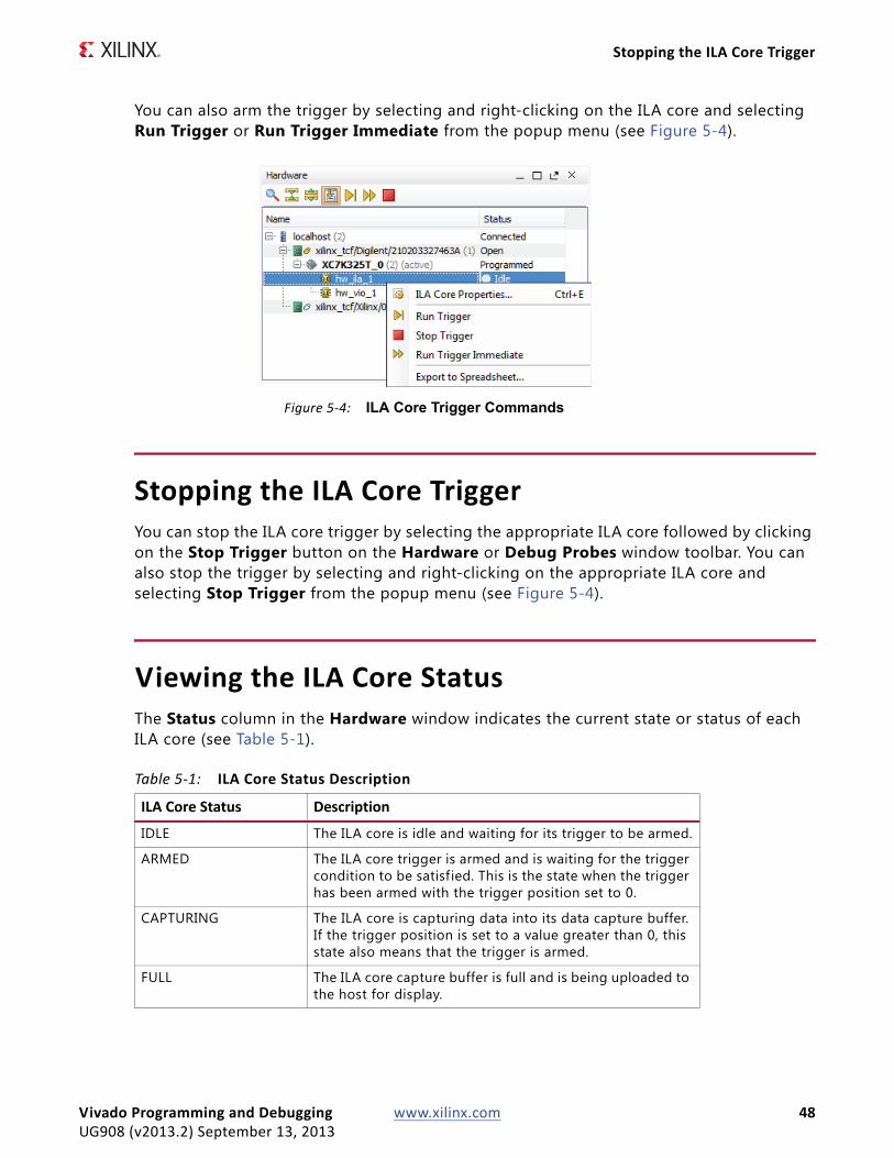
You can also arm the trigger by selecting and right-clicking on the ILA core and selecting Run Trigger or Run Trigger Immediate from the popup menu (see Figure 5-4).
Stopping the ILA Core TriggerYou can stop the ILA core trigger by selecting the appropriate ILA core followed by clicking on the Stop Trigger button on the Hardware or Debug Probes window toolbar. You can also stop the trigger by selecting and right-clicking on the appropriate ILA core and selecting Stop Trigger from the popup menu (see Figure 5-4).
Viewing the ILA Core StatusThe Status column in the Hardware window indicates the current state or status of each ILA core (see Table 5-1).
X-Ref Target - Figure 5-4
Figure 5-4: ILA Core Trigger Commands
Table 5-1: ILA Core Status Description
ILA Core Status Description
IDLE The ILA core is idle and waiting for its trigger to be armed.
ARMED The ILA core trigger is armed and is waiting for the trigger condition to be satisfied. This is the state when the trigger has been armed with the trigger position set to 0.
CAPTURING The ILA core is capturing data into its data capture buffer. If the trigger position is set to a value greater than 0, this state also means that the trigger is armed.
FULL The ILA core capture buffer is full and is being uploaded to the host for display.
Vivado Programming and Debugging www.xilinx.com 48UG908 (v2013.2) September 13, 2013
Viewing Captured Data from the ILA Core in the Waveform Viewer
Viewing Captured Data from the ILA Core in the Waveform ViewerOnce the ILA core captured data has been uploaded to the Vivado IDE, it is displayed in the Waveform Viewer. See Chapter 6, Viewing ILA Probe Data Using Waveform Viewer for details on using the Waveform Viewer to view captured data from the ILA core.
Saving and Restoring Captured Data from the ILA CoreIn addition to displaying the captured data that is directly uploaded from the ILA core, you can also write the captured data to a f ile then read the data from a f ile and display it in the waveform viewer.
Saving Captured ILA Data to a FileCurrently, the only way to upload captured data from an ILA core and save it to a f ile is to use the following Tcl command:
write_hw_ila_data my_hw_ila_data_file.zip [upload_hw_ila_data hw_ila_1]
This Tcl command sequence uploads the captured data from the ILA core and writes it to an archive file called my_hw_ila_data_file.zip. The archive f ile contains the waveform database f ile, the waveform configuration f ile, a waveform comma separated value file, and a debug probes file.
Restoring Captured ILA Data from a FileCurrently, the only way to restore captured data from a file and display it in the waveform viewer is to use the following Tcl command:
display_hw_ila_data [read_hw_ila_data my_hw_ila_data_file.zip]
This Tcl command sequence reads the previously saved captured data from the ILA core and displays it in the waveform window.
Note: The waveform configuration settings (dividers, markers, colors, probe radices, etc.) for the ILA data waveform window will also be saved in the ILA captured data archive f ile. Restoring and displaying any previously saved ILA data will use these stored waveform configuration settings.
Vivado Programming and Debugging www.xilinx.com 49UG908 (v2013.2) September 13, 2013
Setting Up the VIO Core to Take a Measurement
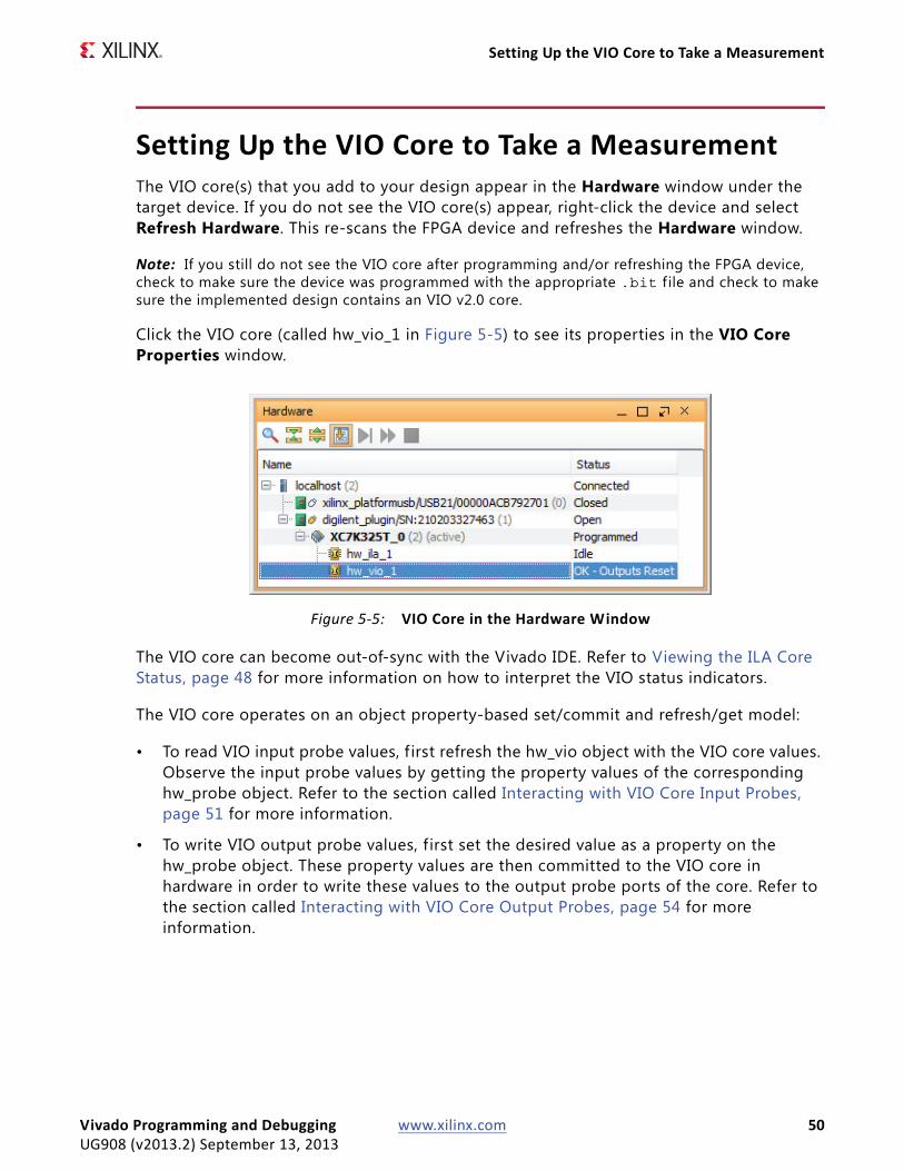
Setting Up the VIO Core to Take a MeasurementThe VIO core(s) that you add to your design appear in the Hardware window under the target device. If you do not see the VIO core(s) appear, right-click the device and select Refresh Hardware. This re-scans the FPGA device and refreshes the Hardware window.
Note: If you still do not see the VIO core after programming and/or refreshing the FPGA device, check to make sure the device was programmed with the appropriate .bit f ile and check to make sure the implemented design contains an VIO v2.0 core.
Click the VIO core (called hw_vio_1 in Figure 5-5) to see its properties in the VIO Core Properties window.
The VIO core can become out-of-sync with the Vivado IDE. Refer to Viewing the ILA Core Status, page 48 for more information on how to interpret the VIO status indicators.
The VIO core operates on an object property-based set/commit and refresh/get model:
• To read VIO input probe values, f irst refresh the hw_vio object with the VIO core values. Observe the input probe values by getting the property values of the corresponding hw_probe object. Refer to the section called Interacting with VIO Core Input Probes, page 51 for more information.
• To write VIO output probe values, f irst set the desired value as a property on the hw_probe object. These property values are then committed to the VIO core in hardware in order to write these values to the output probe ports of the core. Refer to the section called Interacting with VIO Core Output Probes, page 54 for more information.
X-Ref Target - Figure 5-5
Figure 5-5: VIO Core in the Hardware Window
Vivado Programming and Debugging www.xilinx.com 50UG908 (v2013.2) September 13, 2013
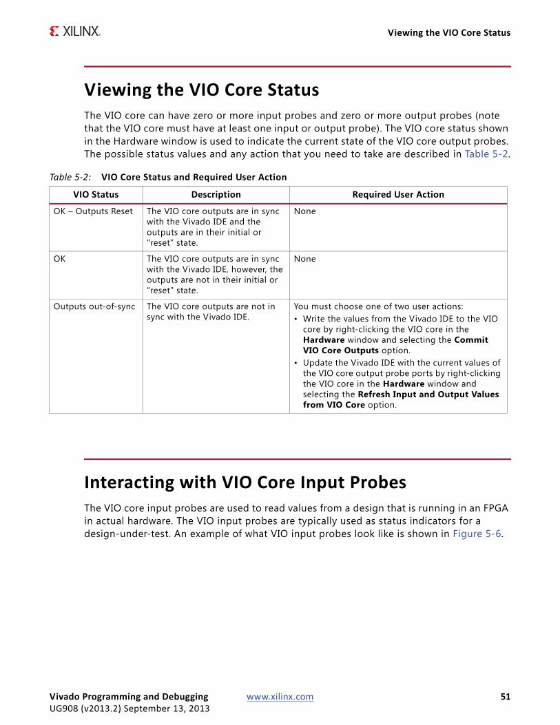
Viewing the VIO Core Status
Viewing the VIO Core StatusThe VIO core can have zero or more input probes and zero or more output probes (note that the VIO core must have at least one input or output probe). The VIO core status shown in the Hardware window is used to indicate the current state of the VIO core output probes. The possible status values and any action that you need to take are described in Table 5-2.
Interacting with VIO Core Input ProbesThe VIO core input probes are used to read values from a design that is running in an FPGA in actual hardware. The VIO input probes are typically used as status indicators for a design-under-test. An example of what VIO input probes look like is shown in Figure 5-6.
Table 5-2: VIO Core Status and Required User Action
VIO Status Description Required User Action
OK – Outputs Reset The VIO core outputs are in sync with the Vivado IDE and the outputs are in their initial or "reset” state.
None
OK The VIO core outputs are in sync with the Vivado IDE, however, the outputs are not in their initial or “reset” state.
None
Outputs out-of-sync The VIO core outputs are not in sync with the Vivado IDE.
You must choose one of two user actions:• Write the values from the Vivado IDE to the VIO
core by right-clicking the VIO core in the Hardware window and selecting the Commit VIO Core Outputs option.
• Update the Vivado IDE with the current values of the VIO core output probe ports by right-clicking the VIO core in the Hardware window and selecting the Refresh Input and Output Values from VIO Core option.
Vivado Programming and Debugging www.xilinx.com 51UG908 (v2013.2) September 13, 2013
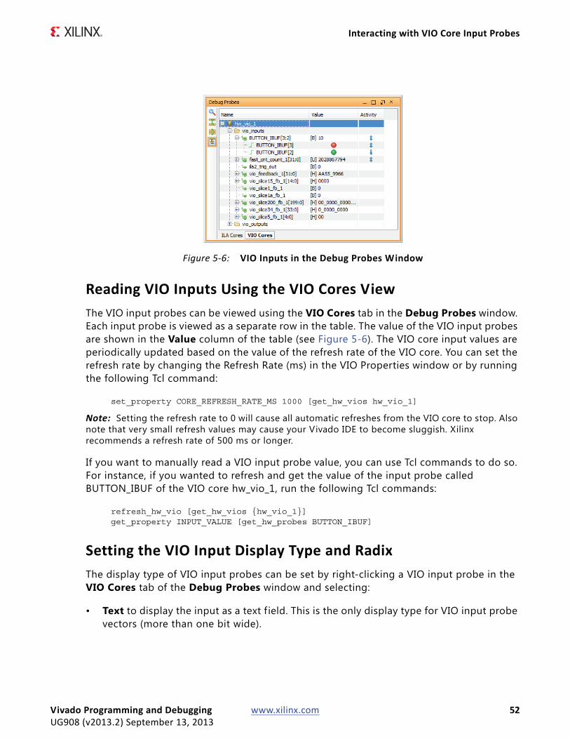
Interacting with VIO Core Input Probes
Reading VIO Inputs Using the VIO Cores ViewThe VIO input probes can be viewed using the VIO Cores tab in the Debug Probes window. Each input probe is viewed as a separate row in the table. The value of the VIO input probes are shown in the Value column of the table (see Figure 5-6). The VIO core input values are periodically updated based on the value of the refresh rate of the VIO core. You can set the refresh rate by changing the Refresh Rate (ms) in the VIO Properties window or by running the following Tcl command:
set_property CORE_REFRESH_RATE_MS 1000 [get_hw_vios hw_vio_1]
Note: Setting the refresh rate to 0 will cause all automatic refreshes from the VIO core to stop. Also note that very small refresh values may cause your Vivado IDE to become sluggish. Xilinx recommends a refresh rate of 500 ms or longer.
If you want to manually read a VIO input probe value, you can use Tcl commands to do so. For instance, if you wanted to refresh and get the value of the input probe called BUTTON_IBUF of the VIO core hw_vio_1, run the following Tcl commands:
refresh_hw_vio [get_hw_vios {hw_vio_1}]get_property INPUT_VALUE [get_hw_probes BUTTON_IBUF]
Setting the VIO Input Display Type and RadixThe display type of VIO input probes can be set by right-clicking a VIO input probe in the VIO Cores tab of the Debug Probes window and selecting:
• Text to display the input as a text f ield. This is the only display type for VIO input probe vectors (more than one bit wide).
X-Ref Target - Figure 5-6
Figure 5-6: VIO Inputs in the Debug Probes Window
Vivado Programming and Debugging www.xilinx.com 52UG908 (v2013.2) September 13, 2013
Interacting with VIO Core Input Probes
• LED to display the input as a graphical representation of a light-emitting diode (LED). This display type is only applicable to VIO input probe scalars and individual elements of VIO input probe vectors. You can set the high and low values to one of four colors:
° Gray (off)
° Red
° Green
° Blue
When the display type of the VIO input probe is set to Text, you can change the radix by right-clicking a VIO input probe in the VIO Cores tabbed view of the Debug Probes window and selecting:
• Radix > Binary to change the radix to binary.
• Radix > Octal to change the radix to octal.
• Radix > Hex to change the radix to hexadecimal.
• Radix > Unsigned to change the radix to unsigned decimal.
• Radix > Signed to change the radix to signed decimal.
You can also set the radix of the VIO input probe using a Tcl command. For instance, to change the radix of a VIO input probe called “BUTTON_IBUF”, run the following Tcl command:
set_property INPUT_VALUE_RADIX HEX [get_hw_probes BUTTON_IBUF]
Observing and Controlling VIO Input ActivityIn addition to reading values from the VIO input probes, you can also monitor the activity of the VIO input probes. The activity detectors are used to indicate when the values on the VIO inputs have changed in between periodic updates to the Vivado IDE.
The VIO input probe activity values are shown as arrows in the activity column of the VIO Cores tab of the Debug Probes window:
• An up arrow indicates that the input probe value has transitioned from a 0 to a 1 during the activity persistence interval.
• A down arrow indicates that the input probe value has transitioned from a 1 to a 0 during the activity persistence interval.
• A double-sided arrow indicates that the input probe value has transitioned from a 1 to a 0 and from a 0 to a 1 at least once during the activity persistence interval.
The persistence of how long the input activity status is displayed can be controlled by right-clicking a VIO input probe in the VIO Cores tab of the Debug Probes window and selecting:
Vivado Programming and Debugging www.xilinx.com 53UG908 (v2013.2) September 13, 2013
Interacting with VIO Core Output Probes
• Activity Persistence > Infinite to accumulate and retain the activity value until the user resets it.
• Activity Persistence > Long (80 samples) to accumulate and retain the activity for a longer period of time.
• Activity Persistence > Short (8 samples) to accumulate and retain the activity for a shorter period of time.
You can also set the activity persistence using a Tcl command. For instance, to change the activity persistence on the VIO input probe called BUTTON_IBUF to a long interval, run the following Tcl command:
set_property ACTIVITY_PERSISTENCE LONG [get_hw_probes BUTTON_IBUF]
The activity for all input probes for a given core can be reset by right-clicking the VIO core in the Hardware window and selecting Reset All Input Activity. You can also do this by running the following Tcl command:
reset_hw_vio_activity [get_hw_vios {hw_vio_1}]
TIP: You can change the type, radix, and/or activity persistence of multiple scalar members of a VIO input probe vector by right-clicking the whole probe or multiple members of the probe, then making a menu choice. The menu choice will apply to all selected probe scalars.
Interacting with VIO Core Output ProbesThe VIO core output probes are used to write values to a design that is running in an FPGA in actual hardware. The VIO output probes are typically used as low-bandwidth control signals for a design-under-test. An example of what VIO output probes look like is shown
Vivado Programming and Debugging www.xilinx.com 54UG908 (v2013.2) September 13, 2013
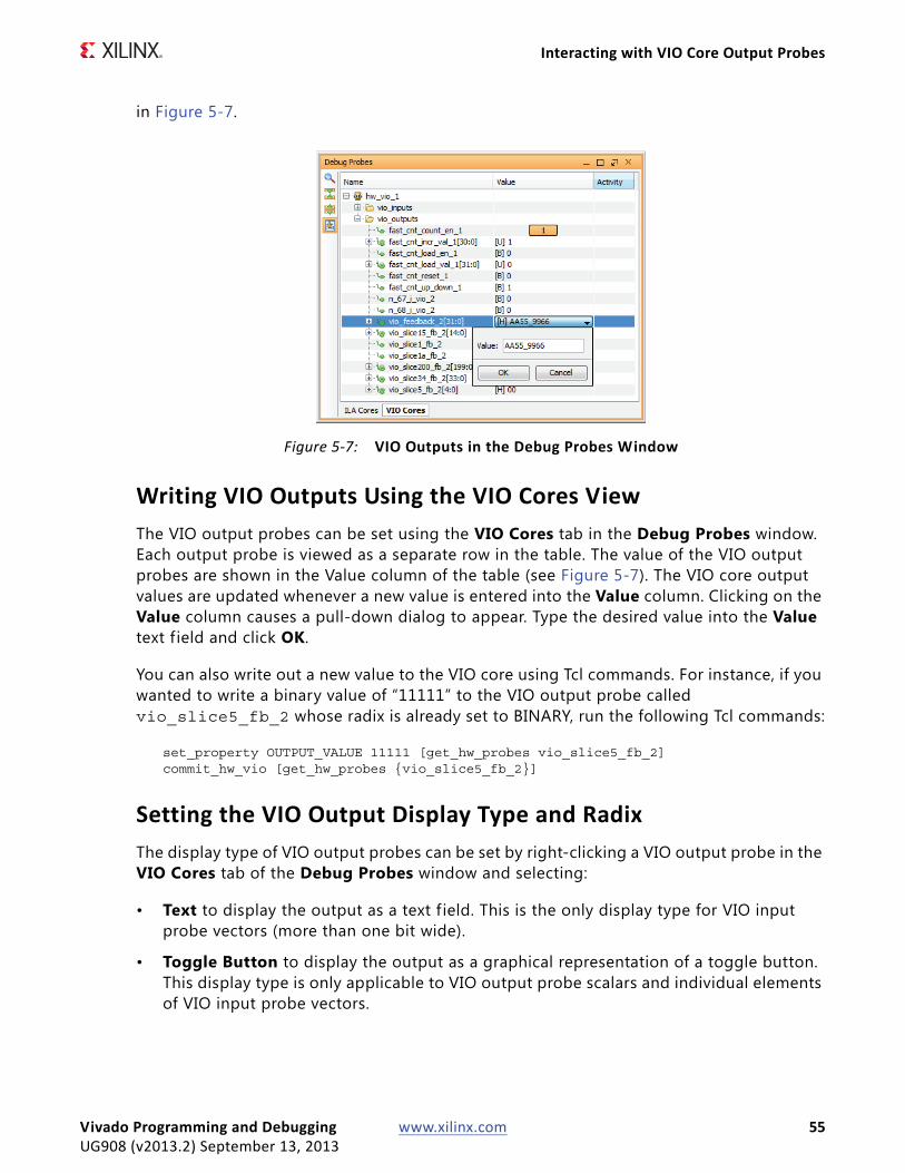
Interacting with VIO Core Output Probes
in Figure 5-7.
Writing VIO Outputs Using the VIO Cores ViewThe VIO output probes can be set using the VIO Cores tab in the Debug Probes window. Each output probe is viewed as a separate row in the table. The value of the VIO output probes are shown in the Value column of the table (see Figure 5-7). The VIO core output values are updated whenever a new value is entered into the Value column. Clicking on the Value column causes a pull-down dialog to appear. Type the desired value into the Value text f ield and click OK.
You can also write out a new value to the VIO core using Tcl commands. For instance, if you wanted to write a binary value of “11111” to the VIO output probe called vio_slice5_fb_2 whose radix is already set to BINARY, run the following Tcl commands:
set_property OUTPUT_VALUE 11111 [get_hw_probes vio_slice5_fb_2]commit_hw_vio [get_hw_probes {vio_slice5_fb_2}]
Setting the VIO Output Display Type and RadixThe display type of VIO output probes can be set by right-clicking a VIO output probe in the VIO Cores tab of the Debug Probes window and selecting:
• Text to display the output as a text f ield. This is the only display type for VIO input probe vectors (more than one bit wide).
• Toggle Button to display the output as a graphical representation of a toggle button. This display type is only applicable to VIO output probe scalars and individual elements of VIO input probe vectors.
X-Ref Target - Figure 5-7
Figure 5-7: VIO Outputs in the Debug Probes Window
Vivado Programming and Debugging www.xilinx.com 55UG908 (v2013.2) September 13, 2013
Interacting with VIO Core Output Probes
When the display type of the VIO output probe is set to “Text”, you can change the radix by right-clicking a VIO output probe in the VIO Cores tabbed view of the Debug Probes window and selecting:
• Radix > Binary to change the radix to binary.
• Radix > Octal to change the radix to octal.
• Radix > Hex to change the radix to hexadecimal.
• Radix > Unsigned to change the radix to unsigned decimal.
• Radix > Signed to change the radix to signed decimal.
You can also set the radix of the VIO output probe using a Tcl command. For instance, to change the radix of a VIO output probe called “vio_slice5_fb_2” to hexadecimal, run the following Tcl command:
set_property OUTPUT_VALUE_RADIX HEX [get_hw_probes vio_slice5_fb_2]
Resetting the VIO Core Output ValuesThe VIO v2.0 core has a feature that allows you to specify an initial value for each output probe port. You can reset the VIO core output probe ports to these initial values by right-clicking the VIO core in the Hardware window and selecting the Reset VIO Core Outputs option. You can also reset the VIO core outputs using a Tcl command:
reset_hw_vio_outputs [get_hw_vios {hw_vio_1}]
Note: Resetting the VIO output probes to their initial values may cause the output probe values to become out-of-sync with the Vivado IDE. Refer to the section called Synchronizing the VIO Core Output Values to the Vivado IDE on how to handle this situation.
Synchronizing the VIO Core Output Values to the Vivado IDEThe output probes of a VIO core can become out-of-sync with the Vivado IDE after resetting the VIO outputs, re-programming the FPGA, or by another Vivado tool instance setting output values before the current instance has started. In any case, if the VIO status indicates “Outputs out-of-sync”, you need to take one of two actions:
• Write the values from the Vivado IDE to the VIO core by right-clicking the VIO core in the Hardware window and selecting the Commit VIO Core Outputs option. You can also do this running a Tcl command:
commit_hw_vio [get_hw_vios {hw_vio_1}]
• Update the Vivado IDE with the current values of the VIO core output probe ports by right-clicking the VIO core in the Hardware window and selecting the Refresh Input and Output Values from VIO Core option. You can also do this running a Tcl command:
refresh_hw_vio -update_output_values 1 [get_hw_vios {hw_vio_1}]
Vivado Programming and Debugging www.xilinx.com 56UG908 (v2013.2) September 13, 2013

Using Vivado Logic Analyzer in a Lab Environment
Using Vivado Logic Analyzer in a Lab EnvironmentThe Vivado logic analyzer feature is integrated into the Vivado IDE. In order to use Vivado logic analyzer feature to debug a design that is running on a target board that is in a lab environment, you need to do one of two things:
• Install and run the full Vivado IDE on your lab machine.
• Install latest version of the Vivado Design Suite on your lab machine, and use the Vivado logic analyzer feature on your local machine to connect to a remote instance of the Vivado CSE Server (vcse_server).
Installing and Running the Full Vivado IDE on a Lab MachineThe requirements for installing the Vivado IDE on your lab machine are found in Vivado Design Suite: Release Notes, Installation and Licensing (UG73) [Ref 4].
IMPORTANT: The Vivado logic analyzer is only compatible with the Vivado CSE server (vcse_server.exe on Windows platforms or vcse_server on Linux platforms) and is not compatible with the legacy CSE server (cse_server.exe on Windows platforms or cse_server on Linux platforms) that is installed as part of the ISE Lab Tools. The legacy CSE server application is only compatible with the legacy ChipScope Pro Analyzer tool. The Vivado logic analyzer only needs two files from the original project: the bitstream programming (.bit) file and the probes (.ltx) file.
Here are the steps to use the Vivado logic analyzer feature on a lab machine.
1. Install the Vivado IDE on your lab machine.
2. Copy the bitstream programming (.bit) f ile and the probes (.ltx) f ile to the lab machine.
3. Start Vivado IDE in GUI mode.
4. Open the hardware session by selecting the File > Open Hardware Session menu option or typing "open_hw" in the Tcl Console window.
5. Follow the steps in the Connecting to the Hardware Target and Programming the FPGA Devices section to open a connection to the target board that is connected to your lab machine. Use the bitstream programming (.bit) f ile that you copied to the lab machine to program target FPGA device.
6. Follow the steps in the Setting up the ILA Core to Take a Measurement section and beyond to debug your design in hardware. Use the probes (.ltx) f ile that you copied to the lab machine when you get to the Reading ILA Probes Information section.
Vivado Programming and Debugging www.xilinx.com 57UG908 (v2013.2) September 13, 2013
Using Vivado Logic Analyzer and ChipScope™ Pro Analyzer Simultaneously
Connecting to a Remote CSE Server Running on a Lab MachineIf you have a network connection to your lab machine, you can also connect to the target board by connecting to a CSE server that is running on that remote lab machine. Here are the steps to using the Vivado logic analyzer feature to connect to a Vivado CSE server (vcse_server.exe on Windows platforms or vcse_server on Linux platforms) that is running on the lab machine:
1. Install the latest version of the Vivado Design Suite on the lab machine.
IMPORTANT: You do NOT need any software licenses to run any of the hardware session features of the Vivado tools (such as the Vivado logic analyzer or Vivado serial I/O analyzer features).
2. Start up the vcse_server application on the remote lab machine. Assuming you installed the Vivado Design Suite to the default location and your lab machine is a 64-bit Windows machine, here is the command line:
C:\Xilinx\Vivado\vivado_release.version\bin\vcse_server.bat -port 60001
3. Start Vivado IDE in GUI mode on a different machine than your lab machine.
4. Follow the steps in the Connecting to the Hardware Target and Programming the FPGA Device section to open a connection to the target board that is connected to your lab machine. However, instead of connecting to a Vivado CSE server running on localhost, use the host name of your lab machine.
5. Follow the steps in the Setting up the ILA Core to Take a Measurement section and beyond to debug your design in hardware.
Using Vivado Logic Analyzer and ChipScope™ Pro Analyzer SimultaneouslyYou can use the Vivado logic analyzer feature and ChipScope™ Pro Analyzer tools to simultaneously debug the same design running on the same target board. Some examples of situations where this capability becomes important are:
• You have a design that contains an ILA v2.1 debug core and a VIO v1.x debug core that you need to interact with using the Vivado logic analyzer feature and ChipScope Pro Analyzer feature, respectively.
• You want to interact with an ILA v2.1 debug core in your design using the Vivado logic analyzer feature and you want to monitor the XADC temperature or voltage sensors using the ChipScope Pro Analyzer tool’s System Monitor feature.
• You have a 7 series device and a 6 series device that you need to debug at the same time using the Vivado logic analyzer feature and the ChipScope Pro Analyzer feature, respectively.
Vivado Programming and Debugging www.xilinx.com 58UG908 (v2013.2) September 13, 2013

Using Vivado Logic Analyzer and ChipScope™ Pro Analyzer Simultaneously
This section covers the f irst case of having both an ILA v2.1 debug core and a VIO v1.x debug core in the same design. The steps that you need to follow to take advantage of this capability are:
1. Use two separate BSCAN user scan chains, one for each JTAG controller core.
2. Start two separate CSE servers, one for each run-time analyzer applications.
3. Use two different run-time analyzer applications, the Vivado logic analyzer feature and ChipScope Pro Analyzer tool.
Using Separate BSCAN User Scan ChainsMake sure that the debug_core_hub core (which is used to connect the ILA v2.1 core to a BSCANE2 primitive) and the ICON v1.x core (which is used to connect the VIO v1.x core to a BSCANE2 primitive) are configured to use different user scan chains (see section Changing the BSCAN User Scan Chain of the Debug Core Hub in Chapter 4 for more details).
Setting Up Separate CSE ServersMake sure two separate CSE server instances are running on the machine that is connected to the target board. For instance, on a Windows 64-bit platform, do the following in two separate cmd windows:
1. Make sure the latest version of the Vivado Design Suite and ISE Lab Tools are installed on the lab machine. This example assumes that ISE Lab Tools and Vivado Design Suite are both installed in their default locations.
2. Open the first cmd window and run the following to start the Vivado CSE server.
C:\Xilinx\Vivado\vivado_release.version\bin\vcse_server.bat –port 60001
3. Open the second cmd window and run to start the legacy CSE server.
C:\Xilinx\ise_release.version\LabTools\LabTools\bin\nt64\cse_server –port 50001
The Vivado CSE server running on port 60001 and the legacy CSE server running on port 50001 will be used by the Vivado logic analyzer feature and ChipScope Pro Analyzer tool, respectively.
Running Vivado Logic Analyzer Feature and ChipScope Pro Analyzer ToolNow that you have set up the design and the CSE servers, you can use the Vivado logic analyzer feature and ChipScope Pro Analyze tool to debug the design by following these steps:
1. Start the Vivado IDE in GUI mode.
Vivado Programming and Debugging www.xilinx.com 59UG908 (v2013.2) September 13, 2013
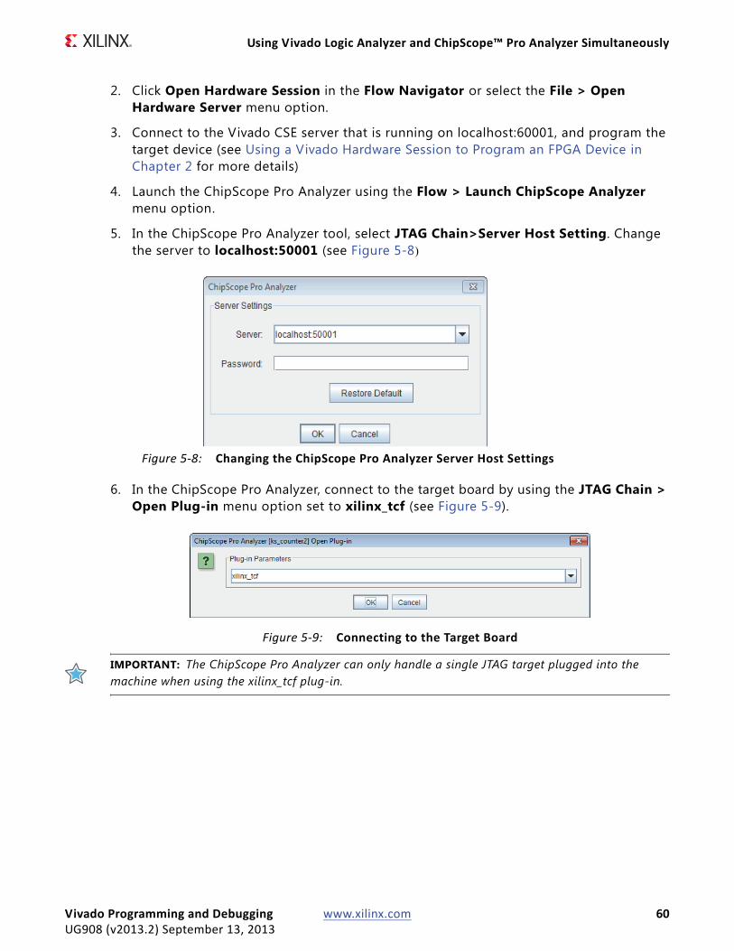
Using Vivado Logic Analyzer and ChipScope™ Pro Analyzer Simultaneously
2. Click Open Hardware Session in the Flow Navigator or select the File > Open Hardware Server menu option.
3. Connect to the Vivado CSE server that is running on localhost:60001, and program the target device (see Using a Vivado Hardware Session to Program an FPGA Device in Chapter 2 for more details)
4. Launch the ChipScope Pro Analyzer using the Flow > Launch ChipScope Analyzer menu option.
5. In the ChipScope Pro Analyzer tool, select JTAG Chain>Server Host Setting. Change the server to localhost:50001 (see Figure 5-8)
6. In the ChipScope Pro Analyzer, connect to the target board by using the JTAG Chain > Open Plug-in menu option set to xilinx_tcf (see Figure 5-9).
IMPORTANT: The ChipScope Pro Analyzer can only handle a single JTAG target plugged into the machine when using the xilinx_tcf plug-in.
X-Ref Target - Figure 5-8
Figure 5-8: Changing the ChipScope Pro Analyzer Server Host Settings
X-Ref Target - Figure 5-9
Figure 5-9: Connecting to the Target Board
Vivado Programming and Debugging www.xilinx.com 60UG908 (v2013.2) September 13, 2013
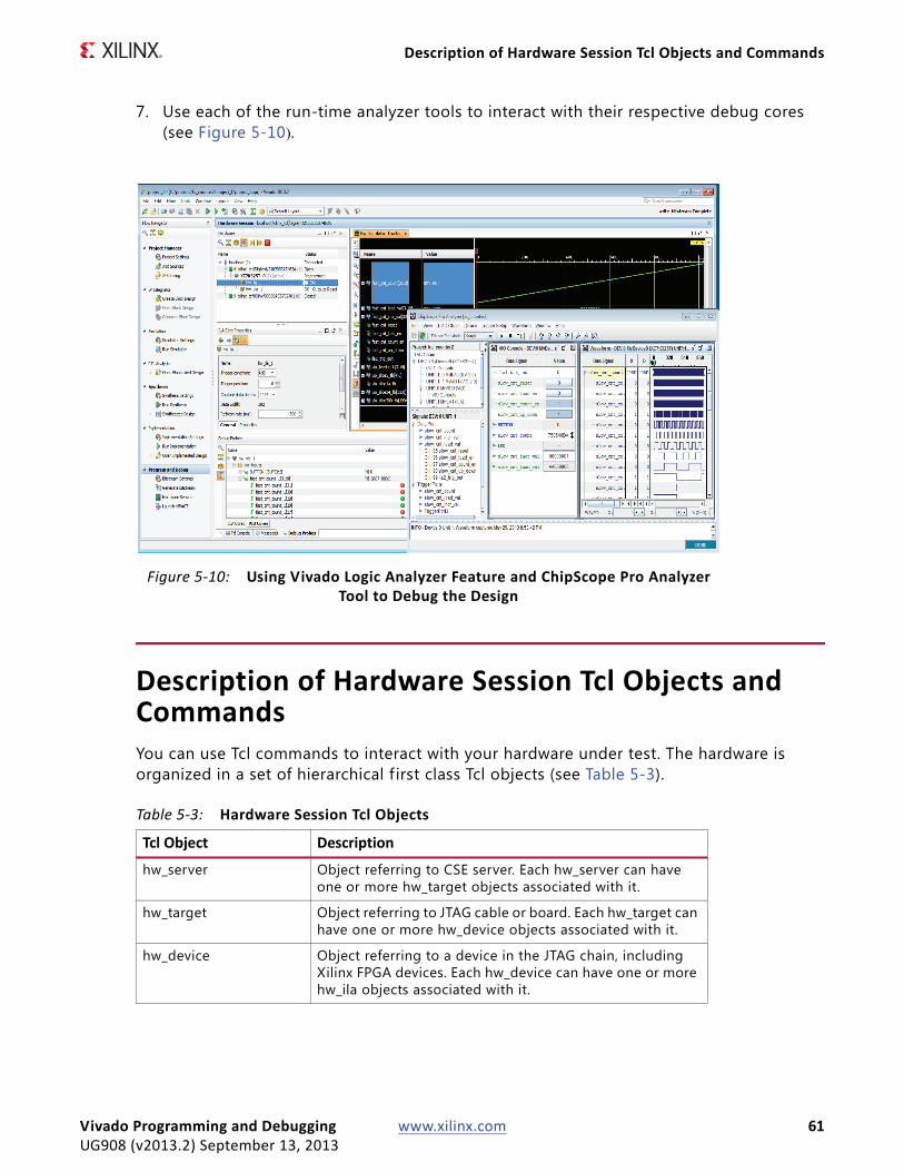
Description of Hardware Session Tcl Objects and Commands
7. Use each of the run-time analyzer tools to interact with their respective debug cores (see Figure 5-10).
Description of Hardware Session Tcl Objects and CommandsYou can use Tcl commands to interact with your hardware under test. The hardware is organized in a set of hierarchical f irst class Tcl objects (see Table 5-3).
X-Ref Target - Figure 5-10
Figure 5-10: Using Vivado Logic Analyzer Feature and ChipScope Pro Analyzer Tool to Debug the Design
Table 5-3: Hardware Session Tcl Objects
Tcl Object Description
hw_server Object referring to CSE server. Each hw_server can have one or more hw_target objects associated with it.
hw_target Object referring to JTAG cable or board. Each hw_target can have one or more hw_device objects associated with it.
hw_device Object referring to a device in the JTAG chain, including Xilinx FPGA devices. Each hw_device can have one or more hw_ila objects associated with it.
Vivado Programming and Debugging www.xilinx.com 61UG908 (v2013.2) September 13, 2013
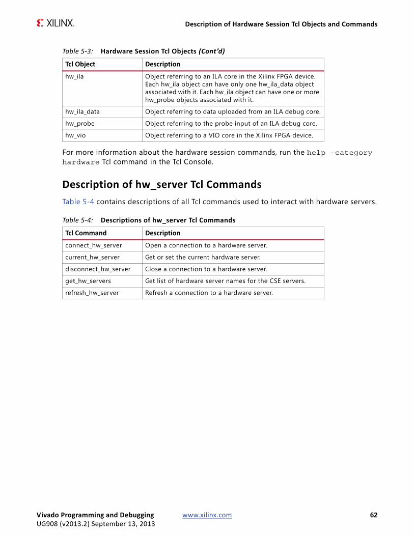
Description of Hardware Session Tcl Objects and Commands
For more information about the hardware session commands, run the help –category hardware Tcl command in the Tcl Console.
Description of hw_server Tcl CommandsTable 5-4 contains descriptions of all Tcl commands used to interact with hardware servers.
hw_ila Object referring to an ILA core in the Xilinx FPGA device. Each hw_ila object can have only one hw_ila_data object associated with it. Each hw_ila object can have one or more hw_probe objects associated with it.
hw_ila_data Object referring to data uploaded from an ILA debug core.
hw_probe Object referring to the probe input of an ILA debug core.
hw_vio Object referring to a VIO core in the Xilinx FPGA device.
Table 5-4: Descriptions of hw_server Tcl Commands
Tcl Command Description
connect_hw_server Open a connection to a hardware server.
current_hw_server Get or set the current hardware server.
disconnect_hw_server Close a connection to a hardware server.
get_hw_servers Get list of hardware server names for the CSE servers.
refresh_hw_server Refresh a connection to a hardware server.
Table 5-3: Hardware Session Tcl Objects (Cont’d)
Tcl Object Description
Vivado Programming and Debugging www.xilinx.com 62UG908 (v2013.2) September 13, 2013
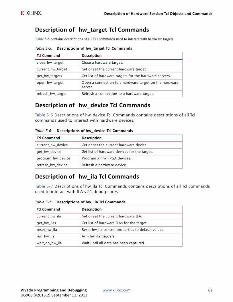
Description of Hardware Session Tcl Objects and Commands
Description of hw_target Tcl CommandsTable 5-5 contains descriptions of all Tcl commands used to interact with hardware targets.
Description of hw_device Tcl CommandsTable 5-6 Descriptions of hw_device Tcl Commands contains descriptions of all Tcl commands used to interact with hardware devices.
Description of hw_ila Tcl CommandsTable 5-7 Descriptions of hw_ila Tcl Commands contains descriptions of all Tcl commands used to interact with ILA v2.1 debug cores.
Table 5-5: Descriptions of hw_target Tcl Commands
Tcl Command Description
close_hw_target Close a hardware target.
current_hw_target Get or set the current hardware target.
get_hw_targets Get list of hardware targets for the hardware servers.
open_hw_target Open a connection to a hardware target on the hardware server.
refresh_hw_target Refresh a connection to a hardware target.
Table 5-6: Descriptions of hw_device Tcl Commands
Tcl Command Description
current_hw_device Get or set the current hardware device.
get_hw_device Get list of hardware devices for the target.
program_hw_device Program Xilinx FPGA devices.
refresh_hw_device Refresh a hardware device.
Table 5-7: Descriptions of hw_ila Tcl Commands
Tcl Command Description
current_hw_ila Get or set the current hardware ILA.
get_hw_ilas Get list of hardware ILAs for the target.
reset_hw_ila Reset hw_ila control properties to default values.
run_hw_ila Arm hw_ila triggers.
wait_on_hw_ila Wait until all data has been captured.
Vivado Programming and Debugging www.xilinx.com 63UG908 (v2013.2) September 13, 2013
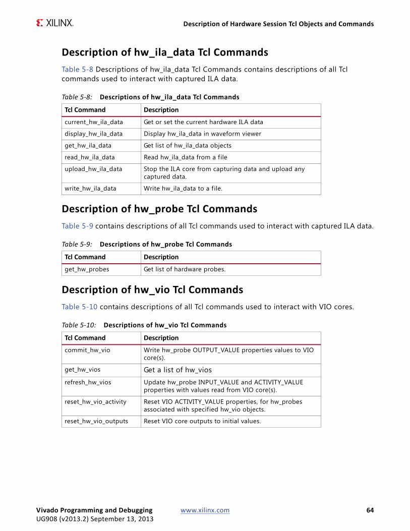
Description of Hardware Session Tcl Objects and Commands
Description of hw_ila_data Tcl CommandsTable 5-8 Descriptions of hw_ila_data Tcl Commands contains descriptions of all Tcl commands used to interact with captured ILA data.
Description of hw_probe Tcl CommandsTable 5-9 contains descriptions of all Tcl commands used to interact with captured ILA data.
Description of hw_vio Tcl CommandsTable 5-10 contains descriptions of all Tcl commands used to interact with VIO cores.
Table 5-8: Descriptions of hw_ila_data Tcl Commands
Tcl Command Description
current_hw_ila_data Get or set the current hardware ILA data
display_hw_ila_data Display hw_ila_data in waveform viewer
get_hw_ila_data Get list of hw_ila_data objects
read_hw_ila_data Read hw_ila_data from a f ile
upload_hw_ila_data Stop the ILA core from capturing data and upload any captured data.
write_hw_ila_data Write hw_ila_data to a file.
Table 5-9: Descriptions of hw_probe Tcl Commands
Tcl Command Description
get_hw_probes Get list of hardware probes.
Table 5-10: Descriptions of hw_vio Tcl Commands
Tcl Command Description
commit_hw_vio Write hw_probe OUTPUT_VALUE properties values to VIO core(s).
get_hw_vios Get a list of hw_vios
refresh_hw_vios Update hw_probe INPUT_VALUE and ACTIVITY_VALUE properties with values read from VIO core(s).
reset_hw_vio_activity Reset VIO ACTIVITY_VALUE properties, for hw_probes associated with specified hw_vio objects.
reset_hw_vio_outputs Reset VIO core outputs to initial values.
Vivado Programming and Debugging www.xilinx.com 64UG908 (v2013.2) September 13, 2013
Using Hardware Session Tcl Commands
Using Hardware Session Tcl CommandsBelow is an example Tcl command script that interacts with the following example system:
• One KC705 board’s Digilent JTAG-SMT1 cable (serial number 12345) accessible via a Vivado CSE server running on localhost:60001.
• Single ILA core in a design running in the XC7K325T device on the KC705 board.
• ILA core has a probe called counter[3:0].
Example Tcl Command Script# Connect to the Digilent Cable on localhost:60001connect_hw_server -host localhost -port 60001current_hw_target [get_hw_targets */xilinx_tcf/Digilent/12345]open_hw_target
# Program and Refresh the XC7K325T Devicecurrent_hw_device [lindex [get_hw_devices] 0]refresh_hw_device -update_hw_probes false [lindex [get_hw_devices] 0]set_property PROGRAM.FILE {C:/design.bit} [lindex [get_hw_devices] 0]set_property PROBES.FILE {C:/design.ltx} [lindex [get_hw_devices] 0]program_hw_devices [lindex [get_hw_devices] 0]refresh_hw_device [lindex [get_hw_devices] 0]
# Set Up ILA Core Trigger Position and Probe Compare Valuesset_property CONTROL.TRIGGER_POSITION 512 [get_hw_ilas hw_ila_1]set_property COMPARE_VALUE.0 eq4'b0000 [get_hw_probes counter]
# Arm the ILA trigger and wait for it to finish capturing datarun_hw_ila hw_ila_1wait_on_hw_ila hw_ila_1
# Upload the captured ILA data, display it, and write it to a filecurrent_hw_ila_data [upload_hw_ila_data hw_ila_1]display_hw_ila_data [current_hw_ila_data]write_hw_ila_data my_hw_ila_data [current_hw_ila_data]
Vivado Programming and Debugging www.xilinx.com 65UG908 (v2013.2) September 13, 2013
Chapter 6
Viewing ILA Probe Data Using Waveform Viewer
IntroductionWith the Vivado™ Integrated Design Environment (IDE) simulator open, you can begin working with the waveform to analyze your design and debug your code. The Vivado logic analyzer populates design data in other areas, such as the Hardware and the ILA Debug Probes windows.
About Wave Configurations and WindowsAlthough both a wave configuration and a WCFG file refer to the customization of lists of waveforms, there is a conceptual difference between them:
• The wave configuration is an object that is loaded into memory with which you can work.
• The WCFG file is the saved form of a wave configuration on disk.
A wave configuration can have a name or be "Untitled#". The name shows on the view of the Wave Configuration window.
Opening a WCFG FileOpen a WCFG file to use with the ILA waveform window by following the steps described below.
IMPORTANT: Before opening a WCFG file, you must have a waveform window open that contains ILA probes in it, otherwise you get an error.
Vivado Programming and Debugging www.xilinx.com 66UG908 (v2013.2) September 13, 2013
About Wave Configurations and Windows
1. Select File > Open Waveform Configuration.
The Open Waveform Configuration dialog box opens.
2. Locate and select a WCFG file.
3. Click OK
A new waveform window appears showing the captured ILA probe data using the waveform configuration contained in the WCFG file that was just opened.
Note: You now have two waveform windows showing the same data: one waveform window that uses the original waveform configuration, and a second waveform window that uses the newly opened waveform configuration. The underlying waveform data is the same in both windows. You can safely close the original waveform window if you want to continue to use the newly opened waveform configuration.
Note: When you open a WCFG file that contains references to hw_probe objects that are not present in an ILA core, the Vivado logic analyzer ignores those hw_probe objects and omits them from the loaded waveform configuration.
Saving a Wave ConfigurationTo save a wave configuration to a WCFG file, select File > Save Waveform Configuration As, and type a name for the waveform configuration.
IMPORTANT: When saving the waveform configuration to a WCFG file, make sure you select a directory location other than the <project>/.Xil directory. This is a temporary directory whose contents are deleted when Vivado exits. You will lose your WCFG file if you store it in this location
Vivado Programming and Debugging www.xilinx.com 67UG908 (v2013.2) September 13, 2013
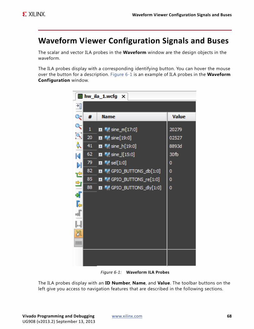
Waveform Viewer Configuration Signals and Buses
Waveform Viewer Configuration Signals and Buses The scalar and vector ILA probes in the Waveform window are the design objects in the waveform.
The ILA probes display with a corresponding identifying button. You can hover the mouse over the button for a description. Figure 6-1 is an example of ILA probes in the Waveform Configuration window.
The ILA probes display with an ID Number, Name, and Value. The toolbar buttons on the left give you access to navigation features that are described in the following sections.
X-Ref Target - Figure 6-1
Figure 6-1: Waveform ILA Probes
Vivado Programming and Debugging www.xilinx.com 68UG908 (v2013.2) September 13, 2013
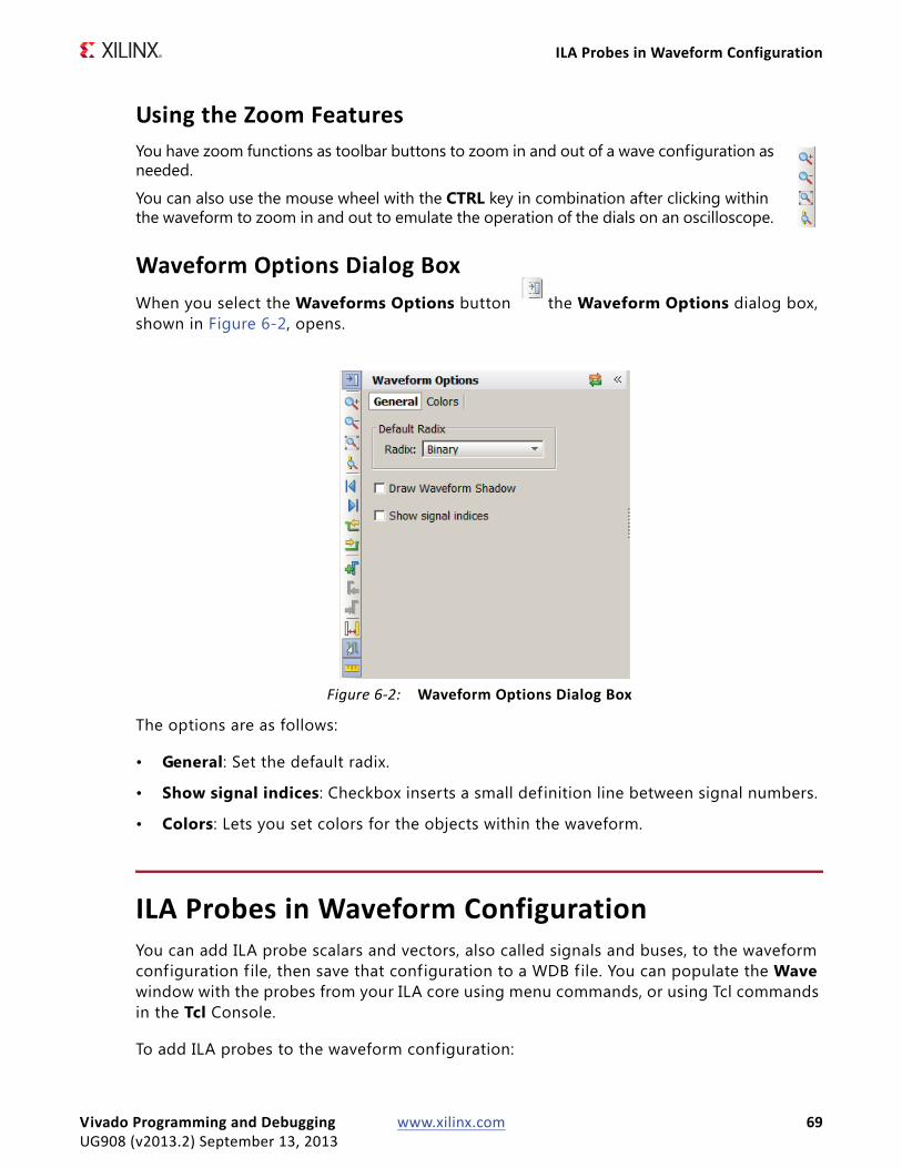
ILA Probes in Waveform Configuration
Using the Zoom FeaturesYou have zoom functions as toolbar buttons to zoom in and out of a wave configuration as needed.
You can also use the mouse wheel with the CTRL key in combination after clicking within the waveform to zoom in and out to emulate the operation of the dials on an oscilloscope.
Waveform Options Dialog BoxWhen you select the Waveforms Options button the Waveform Options dialog box, shown in Figure 6-2, opens.
The options are as follows:
• General: Set the default radix.
• Show signal indices: Checkbox inserts a small definition line between signal numbers.
• Colors: Lets you set colors for the objects within the waveform.
ILA Probes in Waveform ConfigurationYou can add ILA probe scalars and vectors, also called signals and buses, to the waveform configuration f ile, then save that configuration to a WDB file. You can populate the Wave window with the probes from your ILA core using menu commands, or using Tcl commands in the Tcl Console.
To add ILA probes to the waveform configuration:
X-Ref Target - Figure 6-2
Figure 6-2: Waveform Options Dialog Box
Vivado Programming and Debugging www.xilinx.com 69UG908 (v2013.2) September 13, 2013
Customizing the Waveform Configuration
1. In the ILA Cores view of the Debug Probes window, expand the desired ILA core, and select a probe.
2. Right-click, and select Add Probes to Waveform window from the popup menu.
You can add copies of the same signal or bus in a wave configuration for comparing waveforms. You can place copies of the same signal or bus anywhere in the wave configuration, such as in groups or virtual buses.
To add a copy of a signal or bus, do the following:
1. Select a signal or bus in the wave configuration in the Waveform window.
2. Select Edit > Copy or type Ctrl+C.
The signal name is copied to the clipboard.
3. Select Paste or type Ctrl+V.
The signal or bus is now copied to the wave configuration. You can move the signal or bus using drag and drop as needed.
Customizing the Waveform ConfigurationYou can customize the Waveform configuration using the features that are listed and briefly described in Table 6-1; the feature name links to the subsection that fully describes the feature.
Table 6-1: Customization Features in the Waveform Configuration
Feature Description
Cursors The main cursor and secondary cursor in the Waveform window let you display and measure time, and they form the focal point for various navigation activities.
Markers You can add markers to navigate through the waveform, and to display the waveform value at a particular time.
Dividers You can add a divider to create a visual separator of signals.
Using Groups You can add a group, that is a collection to which signals and buses can be added in the wave configuration as a means of organizing a set of related signals.
Using Virtual Buses You can add a virtual bus to your wave configuration, to which you can add logic scalars and arrays.
Renaming Objects You can rename objects, signals, buses, and groups.
Displaying Names You can display the full hierarchical name (long name), the simple signal or bus name (short name), or a custom name for each signal.
Vivado Programming and Debugging www.xilinx.com 70UG908 (v2013.2) September 13, 2013
Customizing the Waveform Configuration
CursorsCursors are used primarily for temporary indicators of sample position and are expected to be moved frequently, as in the case when you are measuring the distance (in samples) between two waveform edges.
TIP: For more permanent indicators, used in situations such as establishing a time-base for multiple measurements, add markers to the Wave window instead. See Markers, page 71 for more information.
You can place the main cursor with a single click in the Waveform window.
To place a secondary cursor, Ctrl+Click and hold the waveform, and drag either left or right. You can see a flag that labels the location at the top of the cursor.
Alternatively, you can hold the SHIFT key and click a point in the waveform. The main cursor remains the original position, and the other cursor is at the point in the waveform that you clicked.
Note: To preserve the location of the secondary cursor while positioning the main cursor, hold the Shift key while clicking. When placing the secondary cursor by dragging, you must drag a minimum distance before the secondary cursor appears.
To move a cursor, hover over the cursor until you see the grab symbol, and click and drag the cursor to the new location.
As you drag the cursor in the Waveform window, you see a hollow or filled-in circle if the Snap to Transition button is selected, which is the default behavior.
• A hollow circle indicates that you are between transitions in the waveform of the selected signal.
• A f illed-in circle indicates that you are hovering over the waveform transition of the selected signal. A secondary cursor can be hidden by clicking anywhere in the Waveform window where there is no cursor, marker, or floating ruler.
MarkersUse a marker when you want to mark a signif icant event within your waveform in a permanent fashion. Markers allow you to measure distance (in samples) relevant to that marked event.
Radixes The default radix controls the bus radix that displays in the wave configuration, Objects panel, and the Console panel.
Bus Bit Order You can change the Bus bit order from Most Signif icant Bit (MSB) to Least Signif icant Bit (LSB) and vice versa.
Table 6-1: Customization Features in the Waveform Configuration (Cont’d)
Feature Description
Vivado Programming and Debugging www.xilinx.com 71UG908 (v2013.2) September 13, 2013

Customizing the Waveform Configuration
You can add, move, and delete markers as follows:
• You add markers to the wave configuration at the location of the main cursor.
a. Place the main cursor at the sample number where you want to add the marker by clicking in the Waveform window at the sample number or on the transition.
b. Select Edit > Markers > Add Marker, or click the Add Marker button.
A marker is placed at the cursor, or slightly offset if a marker already exists at the location of the cursor. The sample number of the marker displays at the top of the line.
• You can move the marker to another location in the waveform using the drag and drop method. Click the marker label (at the top of the marker) and drag it to the location.
° The drag symbol indicates that the marker can be moved. As you drag the marker in the Waveform window, you see a hollow or f illed-in circle if the Snap to Transition button is selected, which is the default behavior.
° A f illed-in circle indicates that you are hovering over a transition of the waveform for the selected signal or over another marker.
° For markers, the f illed-in circle is white.
° A hollow circle indicates that are you between transitions in the waveform of the selected signal.
° Release the mouse key to drop the marker to the new location.
• You can delete one or all markers with one command. Right-click over a marker, and do one of the following:
° Select Delete Marker from the popup menu to delete a single marker.
° Select Delete All Markers from the popup menu to delete all markers.
Note: You can also use the Delete key to delete a selected marker.
° Use Edit > Undo to reverse a marker deletion.
Trigger MarkerThe red trigger marker (whose label is a red letter 'T') is a special marker that indicates the occurrence of the trigger event in the capture buffer. The position of the trigger marker in the buffer directly corresponds to the Trigger Position setting (see section Setting the ILA Core Trigger Position in Chapter 5).
Note: The trigger marker is not movable using the same technique as regular markers. Its position is set using the ILA core's Trigger Position property setting.
Vivado Programming and Debugging www.xilinx.com 72UG908 (v2013.2) September 13, 2013
Customizing the Waveform Configuration
DividersDividers create a visual separator between signals. You can add a divider to your wave configuration to create a visual separator of signals, as follows:
1. In a Name column of the Waveform window, click a signal to add a divider below that signal.
2. From the popup menu, select Edit > New Divider, or right-click and select New Divider.
The change is visual and nothing is added to the HDL code. The new divider is saved with the wave configuration f ile when you save the f ile.
You can move or delete Dividers as follows:
• Move a Divider to another location in the waveform by dragging and dropping the divider name.
• To delete a Divider, highlight the divider, and click the Delete key, or right-click and select Delete from the popup menu.
Dividers can be renamed also; see Renaming Objects, page 75.
Using GroupsA Group is a collection of expandable and collapsible categories, to which you can add signals and buses in the wave configuration to organize related sets of signals. The group itself displays no waveform data but can be expanded to show its contents or collapsed to hide them. You can add, change, and remove groups.
To add a Group:
1. In a wave configuration, select one or more signals or buses to add to a group.
Note: A group can include dividers, virtual buses, and other groups.
2. Select Edit > New Group, or right-click and select New Group from the popup menu.
A Group that contains the selected signal or bus is added to the wave configuration.
A Group is represented with the Group button.
The change is visual and nothing is added to the ILA core.
You can move other signals or buses to the group by dragging and dropping the signal or bus name.
Vivado Programming and Debugging www.xilinx.com 73UG908 (v2013.2) September 13, 2013
Customizing the Waveform Configuration
You can move or remove Groups as follows:
• Move Groups to another location in the Name column by dragging and dropping the group name.
• Remove a group, by highlighting it and selecting Edit > Wave Objects > Ungroup, or right-click and select Ungroup from the popup menu. Signals or buses formerly in the group are placed at the top-level hierarchy in the wave configuration.
Groups can be renamed also; see Renaming Objects, page 75.
CAUTION! The Delete key removes the group and its nested signals and buses from the wave configuration.
Using Virtual BusesYou can add a virtual bus to your wave configuration, which is a grouping to which you can add logic scalars and arrays. The virtual bus displays a bus waveform, which shows the signal waveforms in the vertical order that they appear under the virtual bus, flattened to a one-dimensional array. You can then change or remove virtual buses after adding them.
To add a virtual bus:
1. In a wave configuration, select one or more signals or buses you want to add to a virtual bus.
2. Select Edit > New Virtual Bus, or right-click and select New Virtual Bus from the popup menu.
The virtual bus is represented with the Virtual Bus button .
The change is visual and nothing is added to the HDL code.
You can move other signals or buses to the virtual bus by dragging and dropping the signal or bus name. The new virtual bus and its nested signals or buses are saved when you save the wave configuration f ile. You can also move it to another location in the waveform by dragging and dropping the virtual bus name.
You can rename a virtual bus; see Renaming Objects.
To remove a virtual bus, and ungroup its contents, highlight the virtual bus, and select Edit > Wave Objects > Ungroup, or right-click and select Ungroup from the popup menu.
CAUTION! The Delete key removes the virtual bus and its nested signals and buses from the wave configuration.
Vivado Programming and Debugging www.xilinx.com 74UG908 (v2013.2) September 13, 2013
Renaming Objects
Renaming ObjectsYou can rename any object in the Waveform window, such as signals, dividers, groups, and virtual buses.
1. Select the object name in the Name column.
2. Select Rename from the popup menu.
3. Replace the name with a new one.
4. Press Enter or click outside the name to make the name change take effect.
You can also double-click the object name and then type a new name. The change is effective immediately. Object name changes in the wave configuration do not affect the names of the nets attached to the ILA core probe inputs.
Displaying NamesYou can display the full hierarchical name (long name), the simple signal or bus name (short name), or a custom name for each signal. The signal or bus name displays in the Name column of the wave configuration. If the name is hidden:
• Expand the Name column until you see the entire signal name.
• Use the scroll bar in the Name column to view the name.
To change the display name:
1. Select one or more signal or bus names. Use Shift+ click or Ctrl+ click to select many signal names.
2. Right-click, and select Name >:
° Long to display the full hierarchical name.
° Short to display the name of the signal or bus only.
° Custom to display the custom name given to the signal when renamed.
The name changes immediately according to your selection.
RadixesUnderstanding the type of data on your bus is important. You need to recognize the relationship between the radix setting and the data type to use the waveform options of Digital and Analog effectively. See About Radixes and Analog Waveforms, page 77 for more information about the radix setting and its effect on Analog waveform analysis.
Vivado Programming and Debugging www.xilinx.com 75UG908 (v2013.2) September 13, 2013

Renaming Objects
You can change the radix of an individual signal (ILA probe) in the Waveform window as follows:
1. Right-click a bus in the Waveform window.
2. Select Radix and the format you want from the drop-down menu:
° Binary
° Hexadecimal
° Unsigned Decimal
° Signed Decimal
° Octal
° ASCII
IMPORTANT: Changes to the radix of an item in the Objects window do not apply to values in the Waveform window or the Tcl Console. To change the radix of an individual signal (ILA probe) in the Waveform window, use the Waveform window popup menu.
• Maximum bus width of 64 bits on real. Incorrect values are possible for buses wider than 64 bits.
• Floating point supports only 32- and 64-bit arrays.
Using the Floating RulerThe floating ruler assists with time measurements using a sample number base other than the absolute sample numbers shown on the standard ruler at the top of the Waveform window.
You can display (or hide) a floating ruler and move it to a location in the Waveform window. The sample base (sample 0) of the floating ruler is the secondary cursor, or, if there is no secondary cursor, the selected marker.
The floating ruler button and the floating ruler itself are visible only when the secondary cursor (or selected marker) is present.
1. Do either of the following to display or hide a floating ruler:
° Place the secondary cursor.
° Select a marker.
2. Select View > Floating Ruler, or click the Floating Ruler button.
You only need to follow this procedure the f irst time. The floating ruler displays each time the secondary cursor is placed or a marker is selected.
Select the command again to hide the floating ruler.
Vivado Programming and Debugging www.xilinx.com 76UG908 (v2013.2) September 13, 2013
About Radixes and Analog Waveforms
Bus Bit OrderYou can reverse the bus bit order in the wave configuration to switch between MSB-first and LSB-first signal representation.
To reverse the bit order:
1. Select a bus.
2. Right-click and select Reverse Bit Order.
The bus bit order is reversed. The Reverse Bit Order command is marked to show that this is the current behavior.
About Radixes and Analog WaveformsBus values are interpreted as numeric values, which are determined by the radix setting on the bus wave object, as follows:
• Binary, octal, hexadecimal, ASCII, and unsigned decimal radixes cause the bus values to be interpreted as unsigned integers. The format of data on the bus must match the radix setting.
• Any non-0 or -1 bits cause the entire value to be interpreted as 0.
• The signed decimal radix causes the bus values to be interpreted as signed integers.
• Real radixes cause bus values to be interpreted as f ixed point or floating point real numbers, as determined by the settings of the Real Settings dialog box, shown in Figure 6-3, page 78.
Vivado Programming and Debugging www.xilinx.com 77UG908 (v2013.2) September 13, 2013
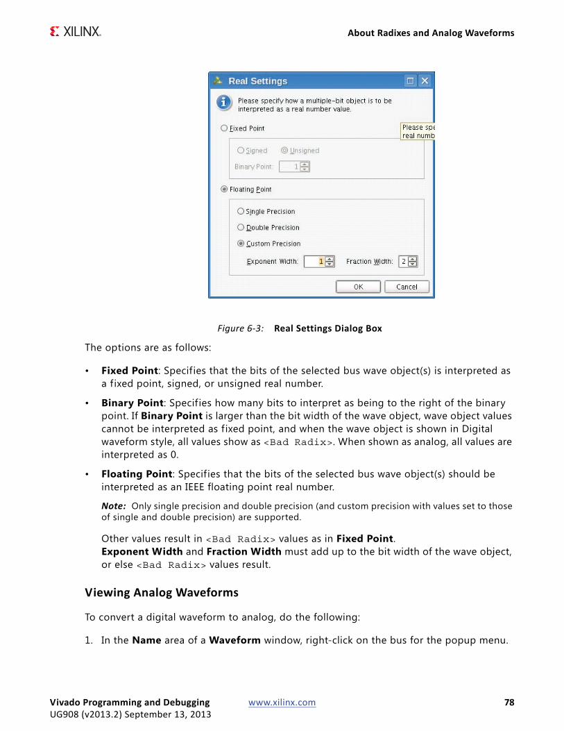
About Radixes and Analog Waveforms
The options are as follows:
• Fixed Point: Specifies that the bits of the selected bus wave object(s) is interpreted as a fixed point, signed, or unsigned real number.
• Binary Point: Specifies how many bits to interpret as being to the right of the binary point. If Binary Point is larger than the bit width of the wave object, wave object values cannot be interpreted as fixed point, and when the wave object is shown in Digital waveform style, all values show as <Bad Radix>. When shown as analog, all values are interpreted as 0.
• Floating Point: Specifies that the bits of the selected bus wave object(s) should be interpreted as an IEEE floating point real number.
Note: Only single precision and double precision (and custom precision with values set to those of single and double precision) are supported.
Other values result in <Bad Radix> values as in Fixed Point. Exponent Width and Fraction Width must add up to the bit width of the wave object, or else <Bad Radix> values result.
Viewing Analog Waveforms
To convert a digital waveform to analog, do the following:
1. In the Name area of a Waveform window, right-click on the bus for the popup menu.
X-Ref Target - Figure 6-3
Figure 6-3: Real Settings Dialog Box
Vivado Programming and Debugging www.xilinx.com 78UG908 (v2013.2) September 13, 2013
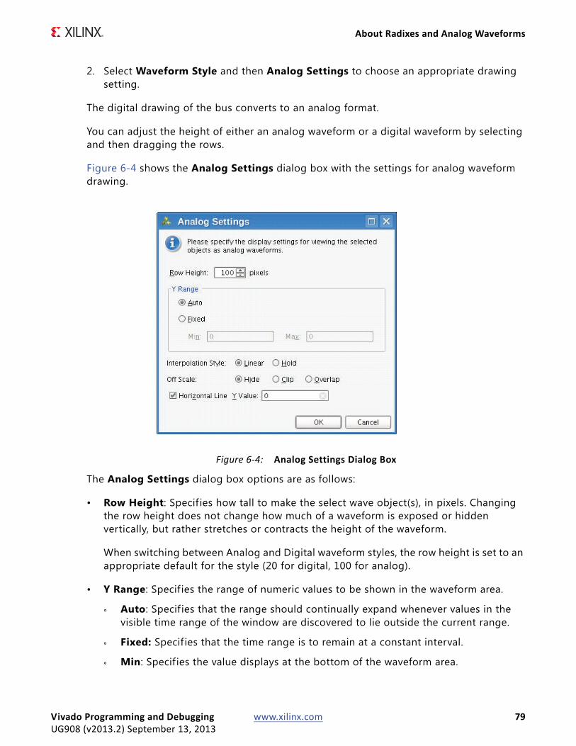
About Radixes and Analog Waveforms
2. Select Waveform Style and then Analog Settings to choose an appropriate drawing setting.
The digital drawing of the bus converts to an analog format.
You can adjust the height of either an analog waveform or a digital waveform by selecting and then dragging the rows.
Figure 6-4 shows the Analog Settings dialog box with the settings for analog waveform drawing.
The Analog Settings dialog box options are as follows:
• Row Height: Specif ies how tall to make the select wave object(s), in pixels. Changing the row height does not change how much of a waveform is exposed or hidden vertically, but rather stretches or contracts the height of the waveform.
When switching between Analog and Digital waveform styles, the row height is set to an appropriate default for the style (20 for digital, 100 for analog).
• Y Range: Specifies the range of numeric values to be shown in the waveform area.
° Auto: Specifies that the range should continually expand whenever values in the visible time range of the window are discovered to lie outside the current range.
° Fixed: Specif ies that the time range is to remain at a constant interval.
° Min: Specifies the value displays at the bottom of the waveform area.
X-Ref Target - Figure 6-4
Figure 6-4: Analog Settings Dialog Box
Vivado Programming and Debugging www.xilinx.com 79UG908 (v2013.2) September 13, 2013
About Radixes and Analog Waveforms
° Max: Specif ies the value displays at the top.
Both values can be specified as floating point; however, if radix of the wave object radix is integral, the values are truncated to integers.
• Interpolation Style: Specif ies how the line connecting data points is to be drawn.
° Linear : Specif ies a straight line between two data points.
° Hold: Specifies that of two data points, a horizontal line is drawn from the left point to the X-coordinate of the right point, then another line is drawn connecting that line to the right data point, in an L shape.
° Off Scale: Specif ies how to draw waveform values that lie outside the Y range of the waveform area.
° Hide: Specifies that outlying values are not shown, such that a waveform that reaches the upper or lower bound of the waveform area disappears until values are again within the range.
° Clip: Specif ies that outlying values be altered so that they are at the top or bottom of the waveform area, such that a waveform that reaches the upper- or lower-bound of the waveform area follows the bound as a horizontal line until values are again within the range.
° Overlap: Specif ies that the waveform be drawn wherever its values are, even if they lie outside the bounds of the waveform area and overlap other waveforms, up to the limits of the wave window itself.
• Horizontal Line: Specif ies whether to draw a horizontal rule at the given value. If the check-box is on, a horizontal grid line is drawn at the vertical position of the specif ied Y value, if that value is within the Y range of the waveform.
As with Min and Max, the Y value accepts a floating point number but truncates it to an integer if the radix of the selected wave objects is integral.
IMPORTANT: Analog settings are saved in a wave configuration; however, because control of zooming in the Y dimension is highly interactive, unlike other wave object properties such as radix, they do not affect the modification state of the wave configuration. Consequently, zoom settings are not saved with the wave configuration.
Vivado Programming and Debugging www.xilinx.com 80UG908 (v2013.2) September 13, 2013
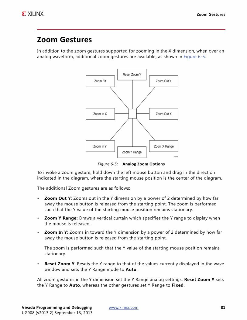
Zoom Gestures
Zoom GesturesIn addition to the zoom gestures supported for zooming in the X dimension, when over an analog waveform, additional zoom gestures are available, as shown in Figure 6-5.
To invoke a zoom gesture, hold down the left mouse button and drag in the direction indicated in the diagram, where the starting mouse position is the center of the diagram.
The additional Zoom gestures are as follows:
• Zoom Out Y: Zooms out in the Y dimension by a power of 2 determined by how far away the mouse button is released from the starting point. The zoom is performed such that the Y value of the starting mouse position remains stationary.
• Zoom Y Range: Draws a vertical curtain which specif ies the Y range to display when the mouse is released.
• Zoom In Y: Zooms in toward the Y dimension by a power of 2 determined by how far away the mouse button is released from the starting point.
The zoom is performed such that the Y value of the starting mouse position remains stationary.
• Reset Zoom Y: Resets the Y range to that of the values currently displayed in the wave window and sets the Y Range mode to Auto.
All zoom gestures in the Y dimension set the Y Range analog settings. Reset Zoom Y sets the Y Range to Auto, whereas the other gestures set Y Range to Fixed.
X-Ref Target - Figure 6-5
Figure 6-5: Analog Zoom Options
Vivado Programming and Debugging www.xilinx.com 81UG908 (v2013.2) September 13, 2013
Chapter 7
In-System Serial I/O Debugging Flows
IntroductionThe Vivado IDE provides a quick and easy way to generate a design that helps you debug and verify your system that uses Xilinx 7 Series high-speed gigabit transceiver (GT) technology. The in-system serial I/O debugging flow has three distinct phases:
1. IBERT Core generation phase: Customizing and generating the IBERT core that best meets your hardware high-speed serial I/O requirements.
2. IBERT Example Design Generation and Implementation phase: Generating the example design for the IBERT core generated in the previous step.
3. Serial I/O Analysis phase: Interacting with the IBERT IP contained in the design to debug and verify issues in your high-speed serial I/O links.
The rest of this chapter will show how to complete the f irst two phases. The third phase is covered in the chapter called Debugging the Serial I/O Design in Hardware.
Generating an IBERT Core using the Vivado IP CatalogThe first phase of getting a suitable hardware design to help debug and validate your system's high-speed serial I/O interfaces is to generate the IBERT core. The following steps outline how to do this:
1. Open the Vivado IDE
2. On the f irst panel, choose Manage IP > New IP Location, then click Next when the Open IP Catalog wizard appears.
3. Select the desired part, target language, target simulator, and IP location. Click Finish.
4. In the IP Catalog under Debug and Verification > Debug, you will f ind one or more available IBERT cores as shown in Figure 7-1, depending on the device selected in the previous step.
Vivado Programming and Debugging www.xilinx.com 82UG908 (v2013.2) September 13, 2013
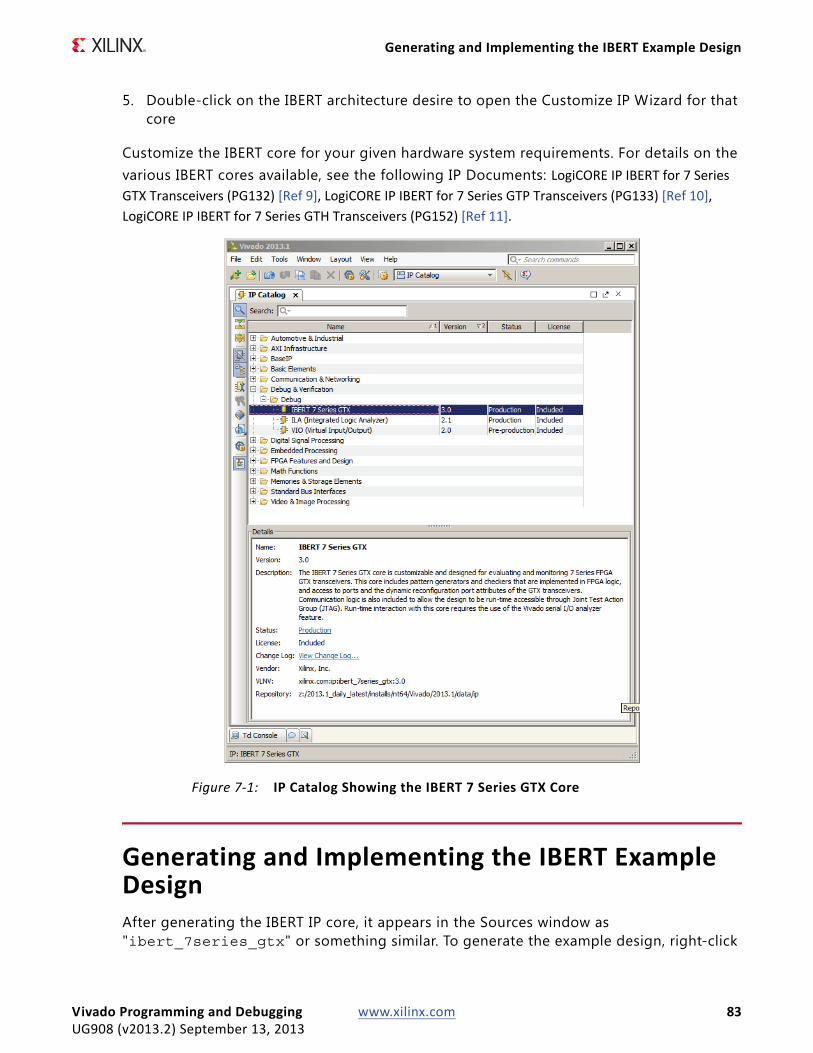
Generating and Implementing the IBERT Example Design
5. Double-click on the IBERT architecture desire to open the Customize IP Wizard for that core
Customize the IBERT core for your given hardware system requirements. For details on the various IBERT cores available, see the following IP Documents: LogiCORE IP IBERT for 7 Series GTX Transceivers (PG132) [Ref 9], LogiCORE IP IBERT for 7 Series GTP Transceivers (PG133) [Ref 10], LogiCORE IP IBERT for 7 Series GTH Transceivers (PG152) [Ref 11].
Generating and Implementing the IBERT Example DesignAfter generating the IBERT IP core, it appears in the Sources window as "ibert_7series_gtx" or something similar. To generate the example design, right-click
X-Ref Target - Figure 7-1
Figure 7-1: IP Catalog Showing the IBERT 7 Series GTX Core
Vivado Programming and Debugging www.xilinx.com 83UG908 (v2013.2) September 13, 2013
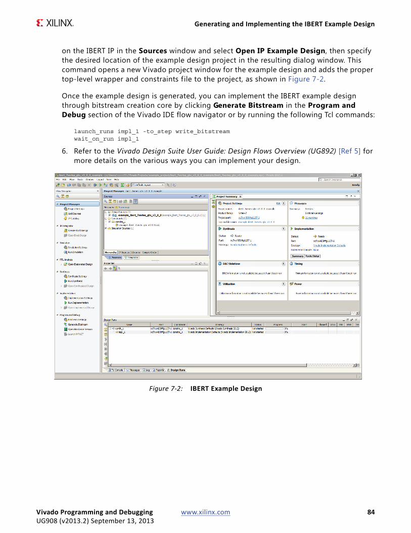
Generating and Implementing the IBERT Example Design
on the IBERT IP in the Sources window and select Open IP Example Design, then specify the desired location of the example design project in the resulting dialog window. This command opens a new Vivado project window for the example design and adds the proper top-level wrapper and constraints f ile to the project, as shown in Figure 7-2.
Once the example design is generated, you can implement the IBERT example design through bitstream creation core by clicking Generate Bitstream in the Program and Debug section of the Vivado IDE flow navigator or by running the following Tcl commands:
launch_runs impl_1 -to_step write_bitstreamwait_on_run impl_1
6. Refer to the Vivado Design Suite User Guide: Design Flows Overview (UG892) [Ref 5] for more details on the various ways you can implement your design.
X-Ref Target - Figure 7-2
Figure 7-2: IBERT Example Design
Vivado Programming and Debugging www.xilinx.com 84UG908 (v2013.2) September 13, 2013
Chapter 8
Debugging the Serial I/O Design in Hardware
IntroductionOnce you have IBERT core implemented, you can use the run-time serial I/O analyzer features to debug the design in hardware. Only IBERT cores version v3.x and later can be accessed using the serial I/O analyzer feature.
Using Vivado Serial I/O Analyzer to Debug the DesignThe Vivado serial I/O analyzer feature is used to interact with IBERT v3.0 debug IP cores that are in your design. To access the Vivado serial I/O analyzer feature, click the Open Hardware Session button in the Program and Debug section of the Flow Navigator.
The steps to debug your design in hardware are:
1. Connect to the hardware target and programming the FPGA device with the bit f ile.
2. Create Links.
3. Modify link settings and examine status.
4. Run scans as needed.
Connecting to the Hardware Target and Programming the FPGA DeviceProgramming an FPGA device prior to debugging involves exactly the same steps described in Using a Vivado Hardware Session to Program an FPGA Device in Chapter 2. After programming the device with the .bit f ile that contains the IBERT v3.0 core, the Hardware window now shows the components of the IBERT core that were detected when scanning the device (see Figure 8-1).
Vivado Programming and Debugging www.xilinx.com 85UG908 (v2013.2) September 13, 2013
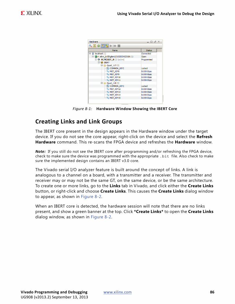
Using Vivado Serial I/O Analyzer to Debug the Design
Creating Links and Link GroupsThe IBERT core present in the design appears in the Hardware window under the target device. If you do not see the core appear, right-click on the device and select the Refresh Hardware command. This re-scans the FPGA device and refreshes the Hardware window.
Note: If you still do not see the IBERT core after programming and/or refreshing the FPGA device, check to make sure the device was programmed with the appropriate .bit f ile. Also check to make sure the implemented design contains an IBERT v3.0 core.
The Vivado serial I/O analyzer feature is built around the concept of links. A link is analogous to a channel on a board, with a transmitter and a receiver. The transmitter and receiver may or may not be the same GT, on the same device, or be the same architecture. To create one or more links, go to the Links tab in Vivado, and click either the Create Links button, or right-click and choose Create Links. This causes the Create Links dialog window to appear, as shown in Figure 8-2.
When an IBERT core is detected, the hardware session will note that there are no links present, and show a green banner at the top. Click *Create Links* to open the Create Links dialog window, as shown in Figure 8-2.
X-Ref Target - Figure 8-1
Figure 8-1: Hardware Window Showing the IBERT Core
Vivado Programming and Debugging www.xilinx.com 86UG908 (v2013.2) September 13, 2013
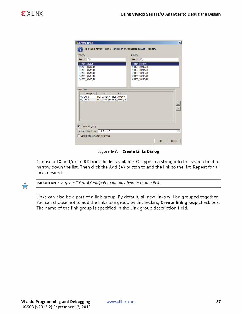
Using Vivado Serial I/O Analyzer to Debug the Design
Choose a TX and/or an RX from the list available. Or type in a string into the search field to narrow down the list. Then click the Add (+) button to add the link to the list. Repeat for all links desired.
IMPORTANT: A given TX or RX endpoint can only belong to one link.
Links can also be a part of a link group. By default, all new links will be grouped together. You can choose not to add the links to a group by unchecking Create link group check box. The name of the link group is specified in the Link group description field.
X-Ref Target - Figure 8-2
Figure 8-2: Create Links Dialog
Vivado Programming and Debugging www.xilinx.com 87UG908 (v2013.2) September 13, 2013
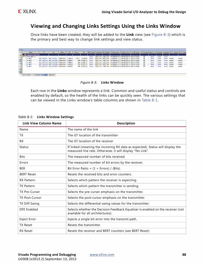
Using Vivado Serial I/O Analyzer to Debug the Design
Viewing and Changing Links Settings Using the Links WindowOnce links have been created, they will be added to the Link view (see Figure 8-3) which is the primary and best way to change link settings and view status.
Each row in the Links window represents a link. Common and useful status and controls are enabled by default, so the health of the links can be quickly seen. The various settings that can be viewed in the Links window’s table columns are shown in Table 8-1.
X-Ref Target - Figure 8-3
Figure 8-3: Links Window
Table 8-1: Links Window Settings
Link View Column Name Description
Name The name of the link
TX The GT location of the transmitter
RX The GT location of the receiver
Status If linked (meaning the incoming RX data as expected). Status will display the measured line rate. Otherwise, it will display “No Link”.
Bits The measured number of bits received.
Errors The measured number of bit errors by the receiver.
BER Bit Error Ratio = (1 + Errors) / (Bits).
BERT Reset Resets the received bits and error counters.
RX Pattern Selects which pattern the receiver is expecting.
TX Pattern Selects which pattern the transmitter is sending.
TX Pre-Curser Selects the pre-curser emphasis on the transmitter.
TX Post-Cursor Selects the post-cursor emphasis on the transmitter.
TX Diff Swing Selects the differential swing values for the transmitter.
DFE Enabled Selects whether the Decision Feedback Equalizer is enabled on the receiver (not available for all architectures).
Inject Error Injects a single bit error into the transmit path.
TX Reset Resets the transmitter.
RX Reset Resets the receiver and BERT counters (see BERT Reset).
Vivado Programming and Debugging www.xilinx.com 88UG908 (v2013.2) September 13, 2013
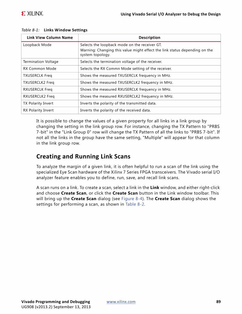
Using Vivado Serial I/O Analyzer to Debug the Design
It is possible to change the values of a given property for all links in a link group by changing the setting in the link group row. For instance, changing the TX Pattern to "PRBS 7-bit" in the "Link Group 0" row will change the TX Pattern of all the links to "PRBS 7-bit". If not all the links in the group have the same setting, "Multiple" will appear for that column in the link group row.
Creating and Running Link ScansTo analyze the margin of a given link, it is often helpful to run a scan of the link using the specialized Eye Scan hardware of the Xilinx 7 Series FPGA transceivers. The Vivado serial I/O analyzer feature enables you to define, run, save, and recall link scans.
A scan runs on a link. To create a scan, select a link in the Link window, and either right-click and choose Create Scan, or click the Create Scan button in the Link window toolbar. This will bring up the Create Scan dialog (see Figure 8-4). The Create Scan dialog shows the settings for performing a scan, as shown in Table 8-2.
Loopback Mode Selects the loopback mode on the receiver GT.Warning: Changing this value might effect the link status depending on the system topology.
Termination Voltage Selects the termination voltage of the receiver.
RX Common Mode Selects the RX Commn Mode setting of the receiver.
TXUSERCLK Freq Shows the measured TXUSERCLK frequency in MHz.
TXUSERCLK2 Freq Shows the measured TXUSERCLK2 frequency in MHz.
RXUSERCLK Freq Shows the measured RXUSERCLK frequency in MHz.
RXUSERCLK2 Freq Shows the measured RXUSERCLK2 frequency in MHz.
TX Polarity Invert Inverts the polarity of the transmitted data.
RX Polarity Invert Inverts the polarity of the received data.
Table 8-1: Links Window Settings
Link View Column Name Description
Vivado Programming and Debugging www.xilinx.com 89UG908 (v2013.2) September 13, 2013
Using Vivado Serial I/O Analyzer to Debug the Design
By default, the scan is run after it is created. If you do not want to run the scan, and only define it, uncheck the Run Scan checkbox.
If a scan is created, but not run, it can be subsequently run or run by right-clicking on a scan in the Scans window and choosing Run Scan (see Figure 8-5). While a scan is running, it can be prematurely stopped by right-clicking on a scan and choosing Stop Scan, or clicking the Stop Scan button in the Scans window toolbar.
X-Ref Target - Figure 8-4
Figure 8-4: Create Scan Dialog
Table 8-2: Scan Settings
Scan Setting Description
Description A user-defined name for the scan.
Scan Type The type of scan to run.
Horizontal Increment Allows the user to choose to scan the eye at a reduced resolution, but at increased speed by skipping horizontal codes.
Horizontal Range Reducing the horizontal range increases the scan speed. By default, the entire eye is scanned (-1/2 of a unit interval to +1/2 in reference to the center of the eye).
Vertical Increment Allows the user to choose to scan the eye at a reduced resolution, but increased speed by skipping vertical codes.
Vertical Range Reducing the vertical range increases the scan speed. By default, the entire eye is scanned.
Dwell BER Each point in the chart is scanned for a certain amount of time. Dwell BER allows the user to choose the scan depth by selecting the desired Bit Error Ratio.
Dwell Time Dwell Time allows the user to choose the scan depth by inputting the desired time in seconds.
Vivado Programming and Debugging www.xilinx.com 90UG908 (v2013.2) September 13, 2013
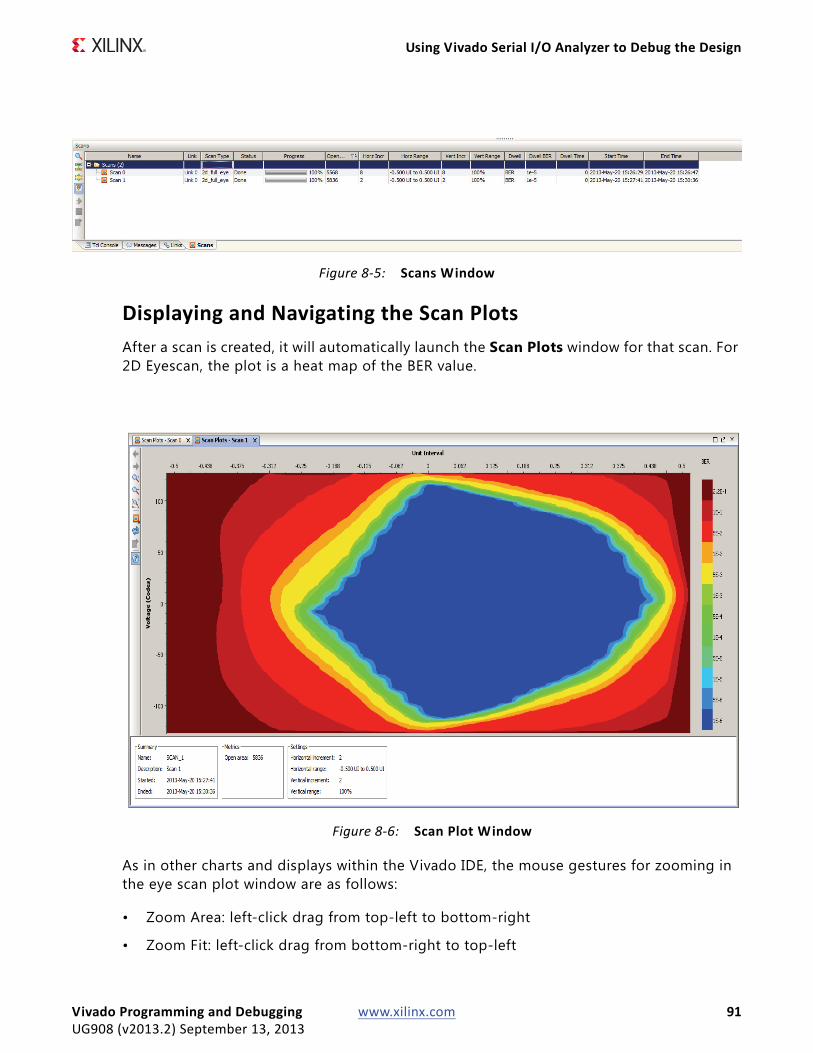
Using Vivado Serial I/O Analyzer to Debug the Design
Displaying and Navigating the Scan PlotsAfter a scan is created, it will automatically launch the Scan Plots window for that scan. For 2D Eyescan, the plot is a heat map of the BER value.
As in other charts and displays within the Vivado IDE, the mouse gestures for zooming in the eye scan plot window are as follows:
• Zoom Area: left-click drag from top-left to bottom-right
• Zoom Fit: left-click drag from bottom-right to top-left
X-Ref Target - Figure 8-5
Figure 8-5: Scans Window
X-Ref Target - Figure 8-6
Figure 8-6: Scan Plot Window
Vivado Programming and Debugging www.xilinx.com 91UG908 (v2013.2) September 13, 2013
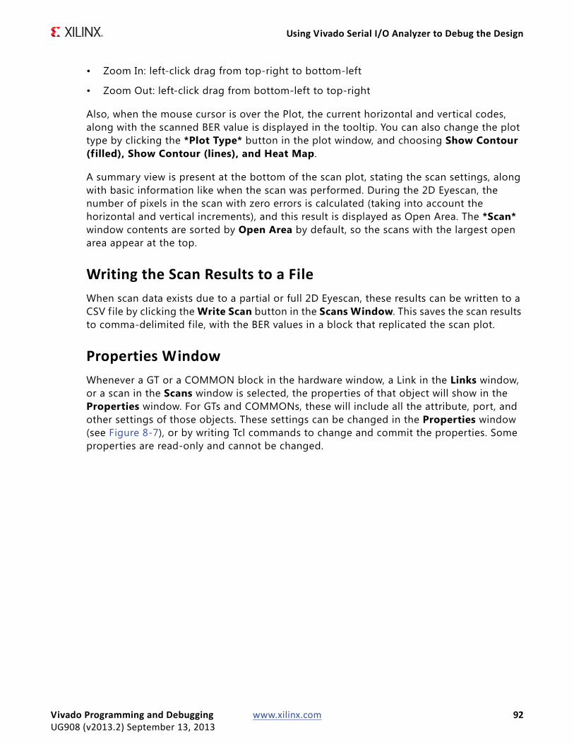
Using Vivado Serial I/O Analyzer to Debug the Design
• Zoom In: left-click drag from top-right to bottom-left
• Zoom Out: left-click drag from bottom-left to top-right
Also, when the mouse cursor is over the Plot, the current horizontal and vertical codes, along with the scanned BER value is displayed in the tooltip. You can also change the plot type by clicking the *Plot Type* button in the plot window, and choosing Show Contour (filled), Show Contour (lines), and Heat Map.
A summary view is present at the bottom of the scan plot, stating the scan settings, along with basic information like when the scan was performed. During the 2D Eyescan, the number of pixels in the scan with zero errors is calculated (taking into account the horizontal and vertical increments), and this result is displayed as Open Area. The *Scan* window contents are sorted by Open Area by default, so the scans with the largest open area appear at the top.
Writing the Scan Results to a FileWhen scan data exists due to a partial or full 2D Eyescan, these results can be written to a CSV f ile by clicking the Write Scan button in the Scans Window. This saves the scan results to comma-delimited f ile, with the BER values in a block that replicated the scan plot.
Properties WindowWhenever a GT or a COMMON block in the hardware window, a Link in the Links window, or a scan in the Scans window is selected, the properties of that object will show in the Properties window. For GTs and COMMONs, these will include all the attribute, port, and other settings of those objects. These settings can be changed in the Properties window (see Figure 8-7), or by writing Tcl commands to change and commit the properties. Some properties are read-only and cannot be changed.
Vivado Programming and Debugging www.xilinx.com 92UG908 (v2013.2) September 13, 2013
Using Vivado Serial I/O Analyzer to Debug the Design
Description of Serial I/O Analyzer Tcl Objects and CommandsYou can use Tcl commands to interact with your hardware under test. The hardware is organized in a set of hierarchical f irst class Tcl objects (see Table 8-3).
X-Ref Target - Figure 8-7
Figure 8-7: Properties Window
Table 8-3: Serial I/O Analyzer Tcl Objects
Tcl Object Description
hw_sio_ibert Object referring to an IBERT core. Each IBERT object can have one or more hw_sio_gt, or hw_sio_common objects associated with it.
hw_sio_gt Object referring to a single Xilinx Gigabit Transceiver (GT).
hw_sio_gtgroups Object referring to a logical grouping of gts, could be a Quad or an Octal.
hw_sio_common Object referring to a COMMON block.
hw_sio_tx Object referring to the transmitter side of a hw_sio_gt. Only the TX related ports, attributes, and logic properties will flow to the hw_sio_tx.
hw_sio_rx Object referring to the receiver side of a hw_sio_gt. Only the RX related ports, attributes, and logic properties will flow to the hw_sio_rx.
Vivado Programming and Debugging www.xilinx.com 93UG908 (v2013.2) September 13, 2013
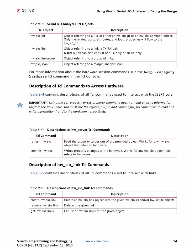
Using Vivado Serial I/O Analyzer to Debug the Design
For more information about the hardware session commands, run the help -category hardware Tcl command in the Tcl Console.
Description of Tcl Commands to Access Hardware
Table 8-4 contains descriptions of all Tcl commands used to interact with the IBERT core.
IMPORTANT: Using the get_property or set_property command does not read or write information to/from the IBERT core. You must use the refresh_hw_sio and commit_hw_sio commands to read and write information from/to the hardware, respectively.
Description of hw_sio_link Tcl Commands
Table 8-5 contains descriptions of all Tcl commands used to interact with links.
hw_sio_pll Object referring to a PLL in either an hw_sio_gt or an hw_sio_common object. Only the related ports, attributes, and logic properties will flow to the hw_sio_pll.
hw_sio_link Object referring to a link, a TX-RX pair. Note: A link can also consist of a TX only or an RX only.
hw_sio_linkgroup Object referring to a group of links.
hw_sio_scan Object referring to a margin analysis scan.
Table 8-3: Serial I/O Analyzer Tcl Objects
Tcl Object Description
Table 8-4: Descriptions of hw_server Tcl Commands
Tcl Command Description
refresh_hw_sio Read the property values out of the provided object. Works for any hw_sio object that refers to hardware.
commit_hw_sio Writes property changes to the hardware. Works for any hw_sio object that refers to hardware.
Table 8-5: Descriptions of hw_sio_link Tcl Commands
Tcl Command Description
create_hw_sio_link Create an hw_sio_link object with the given hw_sio_rx and/or hw_sio_tx objects.
remove_hw_sio_link Deletes the given link.
get_hw_sio_links Get list of hw_sio_links for the given object.
Vivado Programming and Debugging www.xilinx.com 94UG908 (v2013.2) September 13, 2013
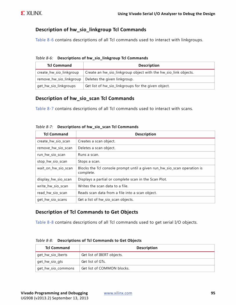
Using Vivado Serial I/O Analyzer to Debug the Design
Description of hw_sio_linkgroup Tcl Commands
Table 8-6 contains descriptions of all Tcl commands used to interact with linkgroups.
Description of hw_sio_scan Tcl Commands
Table 8-7 contains descriptions of all Tcl commands used to interact with scans.
Description of Tcl Commands to Get Objects
Table 8-8 contains descriptions of all Tcl commands used to get serial I/O objects.
Table 8-6: Descriptions of hw_sio_linkgroup Tcl Commands
Tcl Command Description
create_hw_sio_linkgroup Create an hw_sio_linkgroup object with the hw_sio_link objects.
remove_hw_sio_linkgroup Deletes the given linkgroup.
get_hw_sio_linkgroups Get list of hw_sio_linkgroups for the given object.
Table 8-7: Descriptions of hw_sio_scan Tcl Commands
Tcl Command Description
create_hw_sio_scan Creates a scan object.
remove_hw_sio_scan Deletes a scan object.
run_hw_sio_scan Runs a scan.
stop_hw_sio_scan Stops a scan.
wait_on_hw_sio_scan Blocks the Tcl console prompt until a given run_hw_sio_scan operation is complete.
display_hw_sio_scan Displays a partial or complete scan in the Scan Plot.
write_hw_sio_scan Writes the scan data to a file.
read_hw_sio_scan Reads scan data from a f ile into a scan object.
get_hw_sio_scans Get a list of hw_sio_scan objects.
Table 8-8: Descriptions of Tcl Commands to Get Objects
Tcl Command Description
get_hw_sio_iberts Get list of IBERT objects.
get_hw_sio_gts Get list of GTs.
get_hw_sio_commons Get list of COMMON blocks.
Vivado Programming and Debugging www.xilinx.com 95UG908 (v2013.2) September 13, 2013
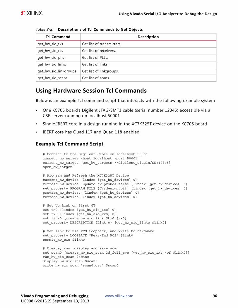
Using Vivado Serial I/O Analyzer to Debug the Design
Using Hardware Session Tcl CommandsBelow is an example Tcl command script that interacts with the following example system
• One KC705 board's Digilent JTAG-SMT1 cable (serial number 12345) accessible via a CSE server running on localhost:50001
• Single IBERT core in a design running in the XC7K325T device on the KC705 board
• IBERT core has Quad 117 and Quad 118 enabled
Example Tcl Command Script
# Connect to the Digilent Cable on localhost:50001connect_hw_server -host localhost -port 50001current_hw_target [get_hw_targets */digilent_plugin/SN:12345]open_hw_target
# Program and Refresh the XC7K325T Devicecurrent_hw_device [lindex [get_hw_devices] 0]refresh_hw_device -update_hw_probes false [lindex [get_hw_devices] 0]set_property PROGRAM.FILE {C:/design.bit} [lindex [get_hw_devices] 0]program_hw_devices [lindex [get_hw_devices] 0]refresh_hw_device [lindex [get_hw_devices] 0]
# Set Up Link on first GT set tx0 [lindex [get_hw_sio_txs] 0]set rx0 [lindex [get_hw_sio_rxs] 0]set link0 [create_hw_sio_link $tx0 $rx0]set_property DESCRIPTION {Link 0} [get_hw_sio_links $link0]
# Set link to use PCS Loopback, and write to hardwareset_property LOOPBACK "Near-End PCS" $link0commit_hw_sio $link0
# Create, run, display and save scanset scan0 [create_hw_sio_scan 2d_full_eye [get_hw_sio_rxs -of $link0]]run_hw_sio_scan $scan0display_hw_sio_scan $scan0write_hw_sio_scan "scan0.csv" $scan0
get_hw_sio_txs Get list of transmitters.
get_hw_sio_rxs Get list of receivers.
get_hw_sio_plls Get list of PLLs.
get_hw_sio_links Get list of links.
get_hw_sio_linkgroups Get list of linkgroups.
get_hw_sio_scans Get list of scans.
Table 8-8: Descriptions of Tcl Commands to Get Objects
Tcl Command Description
Vivado Programming and Debugging www.xilinx.com 96UG908 (v2013.2) September 13, 2013
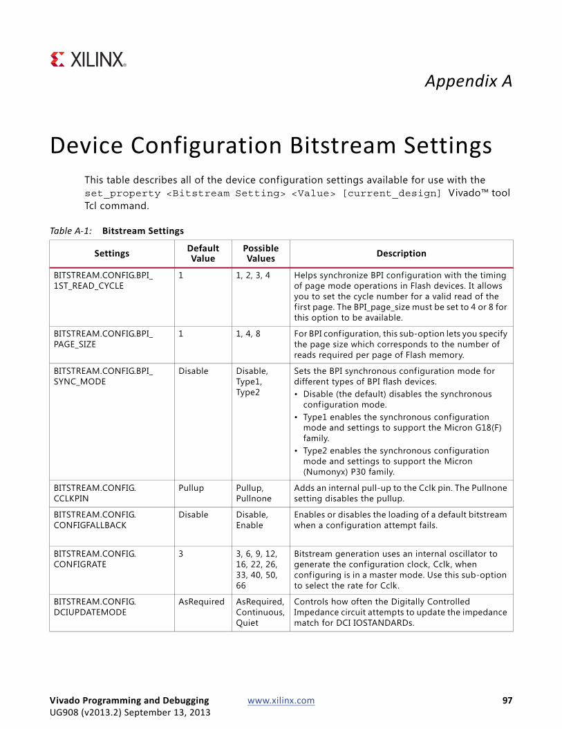
Appendix A
Device Configuration Bitstream SettingsThis table describes all of the device configuration settings available for use with the set_property <Bitstream Setting> <Value> [current_design] Vivado™ tool Tcl command.
Table A-1: Bitstream Settings
Settings Default Value
Possible Values Description
BITSTREAM.CONFIG.BPI_1ST_READ_CYCLE
1 1, 2, 3, 4 Helps synchronize BPI configuration with the timing of page mode operations in Flash devices. It allows you to set the cycle number for a valid read of the first page. The BPI_page_size must be set to 4 or 8 for this option to be available.
BITSTREAM.CONFIG.BPI_PAGE_SIZE
1 1, 4, 8 For BPI configuration, this sub-option lets you specify the page size which corresponds to the number of reads required per page of Flash memory.
BITSTREAM.CONFIG.BPI_SYNC_MODE
Disable Disable, Type1, Type2
Sets the BPI synchronous configuration mode for different types of BPI flash devices.• Disable (the default) disables the synchronous
configuration mode.• Type1 enables the synchronous configuration
mode and settings to support the Micron G18(F) family.
• Type2 enables the synchronous configuration mode and settings to support the Micron (Numonyx) P30 family.
BITSTREAM.CONFIG.CCLKPIN
Pullup Pullup, Pullnone
Adds an internal pull-up to the Cclk pin. The Pullnone setting disables the pullup.
BITSTREAM.CONFIG.CONFIGFALLBACK
Disable Disable, Enable
Enables or disables the loading of a default bitstream when a configuration attempt fails.
BITSTREAM.CONFIG.CONFIGRATE
3 3, 6, 9, 12, 16, 22, 26, 33, 40, 50, 66
Bitstream generation uses an internal oscillator to generate the configuration clock, Cclk, when configuring is in a master mode. Use this sub-option to select the rate for Cclk.
BITSTREAM.CONFIG.DCIUPDATEMODE
AsRequired AsRequired, Continuous, Quiet
Controls how often the Digitally Controlled Impedance circuit attempts to update the impedance match for DCI IOSTANDARDs.
Vivado Programming and Debugging www.xilinx.com 97UG908 (v2013.2) September 13, 2013
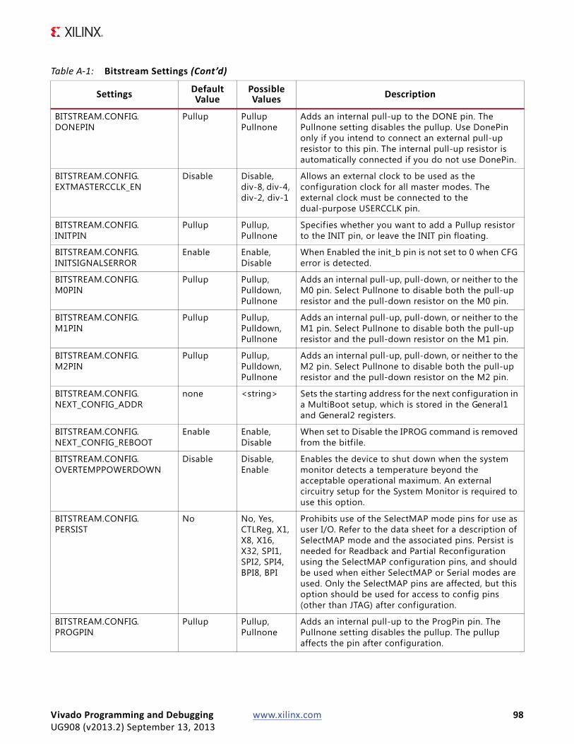
BITSTREAM.CONFIG.DONEPIN
Pullup Pullup Pullnone
Adds an internal pull-up to the DONE pin. The Pullnone setting disables the pullup. Use DonePin only if you intend to connect an external pull-up resistor to this pin. The internal pull-up resistor is automatically connected if you do not use DonePin.
BITSTREAM.CONFIG.EXTMASTERCCLK_EN
Disable Disable, div-8, div-4, div-2, div-1
Allows an external clock to be used as the configuration clock for all master modes. The external clock must be connected to the dual-purpose USERCCLK pin.
BITSTREAM.CONFIG.INITPIN
Pullup Pullup, Pullnone
Specifies whether you want to add a Pullup resistor to the INIT pin, or leave the INIT pin floating.
BITSTREAM.CONFIG.INITSIGNALSERROR
Enable Enable, Disable
When Enabled the init_b pin is not set to 0 when CFG error is detected.
BITSTREAM.CONFIG.M0PIN
Pullup Pullup, Pulldown, Pullnone
Adds an internal pull-up, pull-down, or neither to the M0 pin. Select Pullnone to disable both the pull-up resistor and the pull-down resistor on the M0 pin.
BITSTREAM.CONFIG.M1PIN
Pullup Pullup, Pulldown, Pullnone
Adds an internal pull-up, pull-down, or neither to the M1 pin. Select Pullnone to disable both the pull-up resistor and the pull-down resistor on the M1 pin.
BITSTREAM.CONFIG.M2PIN
Pullup Pullup, Pulldown, Pullnone
Adds an internal pull-up, pull-down, or neither to the M2 pin. Select Pullnone to disable both the pull-up resistor and the pull-down resistor on the M2 pin.
BITSTREAM.CONFIG.NEXT_CONFIG_ADDR
none <string> Sets the starting address for the next configuration in a MultiBoot setup, which is stored in the General1 and General2 registers.
BITSTREAM.CONFIG.NEXT_CONFIG_REBOOT
Enable Enable, Disable
When set to Disable the IPROG command is removed from the bitfile.
BITSTREAM.CONFIG.OVERTEMPPOWERDOWN
Disable Disable, Enable
Enables the device to shut down when the system monitor detects a temperature beyond the acceptable operational maximum. An external circuitry setup for the System Monitor is required to use this option.
BITSTREAM.CONFIG.PERSIST
No No, Yes, CTLReg, X1, X8, X16, X32, SPI1, SPI2, SPI4, BPI8, BPI
Prohibits use of the SelectMAP mode pins for use as user I/O. Refer to the data sheet for a description of SelectMAP mode and the associated pins. Persist is needed for Readback and Partial Reconfiguration using the SelectMAP configuration pins, and should be used when either SelectMAP or Serial modes are used. Only the SelectMAP pins are affected, but this option should be used for access to config pins (other than JTAG) after configuration.
BITSTREAM.CONFIG.PROGPIN
Pullup Pullup, Pullnone
Adds an internal pull-up to the ProgPin pin. The Pullnone setting disables the pullup. The pullup affects the pin after configuration.
Table A-1: Bitstream Settings (Cont’d)
Settings Default Value
Possible Values Description
Vivado Programming and Debugging www.xilinx.com 98UG908 (v2013.2) September 13, 2013
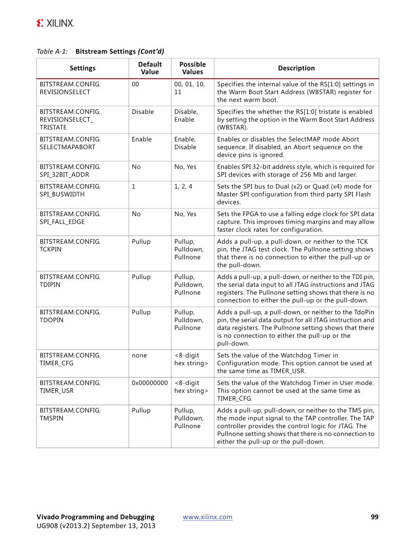
BITSTREAM.CONFIG.REVISIONSELECT
00 00, 01, 10, 11
Specifies the internal value of the RS[1:0] settings in the Warm Boot Start Address (WBSTAR) register for the next warm boot.
BITSTREAM.CONFIG.REVISIONSELECT_TRISTATE
Disable Disable, Enable
Specifies the whether the RS[1:0] tristate is enabled by setting the option in the Warm Boot Start Address (WBSTAR).
BITSTREAM.CONFIG.SELECTMAPABORT
Enable Enable, Disable
Enables or disables the SelectMAP mode Abort sequence. If disabled, an Abort sequence on the device pins is ignored.
BITSTREAM.CONFIG.SPI_32BIT_ADDR
No No, Yes Enables SPI 32-bit address style, which is required for SPI devices with storage of 256 Mb and larger.
BITSTREAM.CONFIG.SPI_BUSWIDTH
1 1, 2, 4 Sets the SPI bus to Dual (x2) or Quad (x4) mode for Master SPI configuration from third party SPI Flash devices.
BITSTREAM.CONFIG.SPI_FALL_EDGE
No No, Yes Sets the FPGA to use a falling edge clock for SPI data capture. This improves timing margins and may allow faster clock rates for configuration.
BITSTREAM.CONFIG.TCKPIN
Pullup Pullup, Pulldown, Pullnone
Adds a pull-up, a pull-down, or neither to the TCK pin, the JTAG test clock. The Pullnone setting shows that there is no connection to either the pull-up or the pull-down.
BITSTREAM.CONFIG.TDIPIN
Pullup Pullup, Pulldown, Pullnone
Adds a pull-up, a pull-down, or neither to the TDI pin, the serial data input to all JTAG instructions and JTAG registers. The Pullnone setting shows that there is no connection to either the pull-up or the pull-down.
BITSTREAM.CONFIG.TDOPIN
Pullup Pullup, Pulldown, Pullnone
Adds a pull-up, a pull-down, or neither to the TdoPin pin, the serial data output for all JTAG instruction and data registers. The Pullnone setting shows that there is no connection to either the pull-up or the pull-down.
BITSTREAM.CONFIG.TIMER_CFG
none <8-digit hex string>
Sets the value of the Watchdog Timer in Configuration mode. This option cannot be used at the same time as TIMER_USR.
BITSTREAM.CONFIG.TIMER_USR
0x00000000 <8-digit hex string>
Sets the value of the Watchdog Timer in User mode. This option cannot be used at the same time as TIMER_CFG.
BITSTREAM.CONFIG.TMSPIN
Pullup Pullup, Pulldown, Pullnone
Adds a pull-up, pull-down, or neither to the TMS pin, the mode input signal to the TAP controller. The TAP controller provides the control logic for JTAG. The Pullnone setting shows that there is no connection to either the pull-up or the pull-down.
Table A-1: Bitstream Settings (Cont’d)
Settings Default Value
Possible Values Description
Vivado Programming and Debugging www.xilinx.com 99UG908 (v2013.2) September 13, 2013
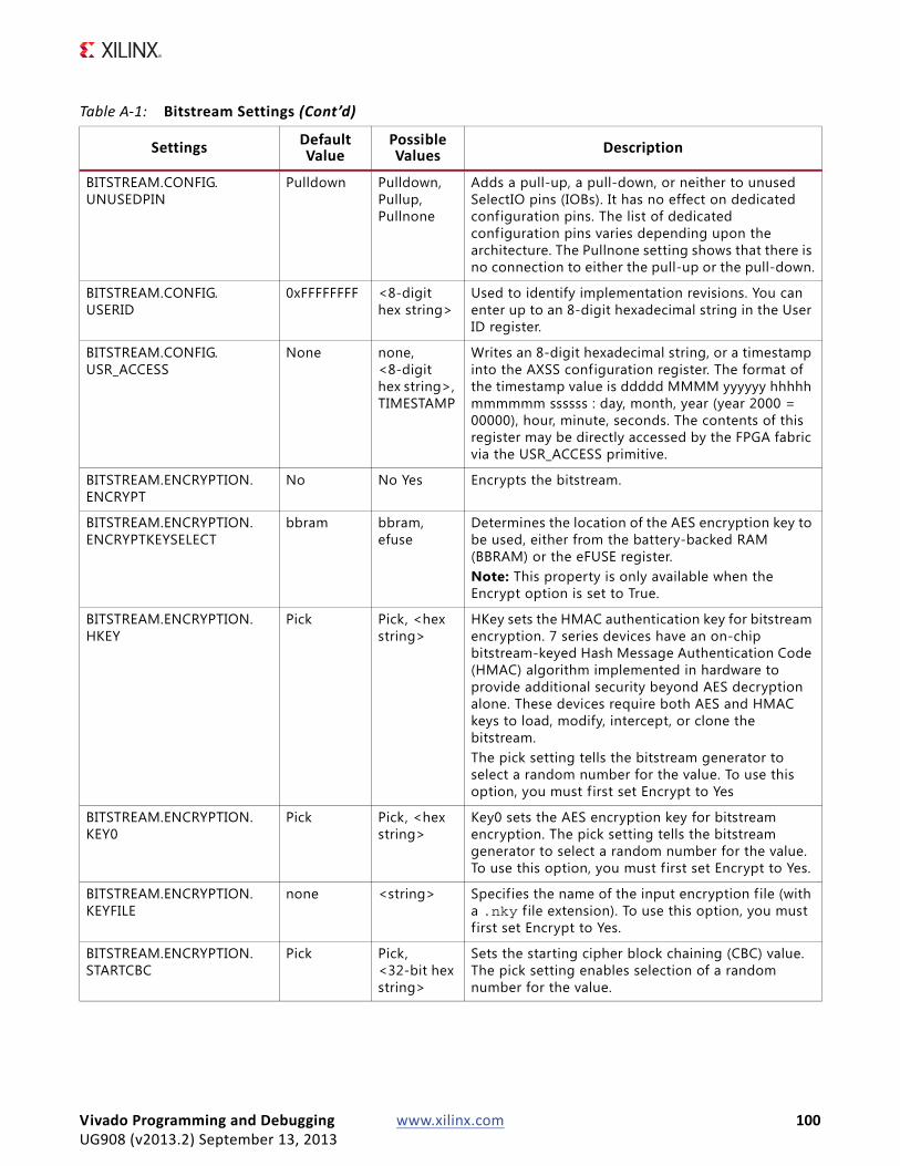
BITSTREAM.CONFIG.UNUSEDPIN
Pulldown Pulldown, Pullup, Pullnone
Adds a pull-up, a pull-down, or neither to unused SelectIO pins (IOBs). It has no effect on dedicated configuration pins. The list of dedicated configuration pins varies depending upon the architecture. The Pullnone setting shows that there is no connection to either the pull-up or the pull-down.
BITSTREAM.CONFIG.USERID
0xFFFFFFFF <8-digit hex string>
Used to identify implementation revisions. You can enter up to an 8-digit hexadecimal string in the User ID register.
BITSTREAM.CONFIG.USR_ACCESS
None none, <8-digit hex string>, TIMESTAMP
Writes an 8-digit hexadecimal string, or a timestamp into the AXSS configuration register. The format of the timestamp value is ddddd MMMM yyyyyy hhhhh mmmmmm ssssss : day, month, year (year 2000 = 00000), hour, minute, seconds. The contents of this register may be directly accessed by the FPGA fabric via the USR_ACCESS primitive.
BITSTREAM.ENCRYPTION.ENCRYPT
No No Yes Encrypts the bitstream.
BITSTREAM.ENCRYPTION.ENCRYPTKEYSELECT
bbram bbram, efuse
Determines the location of the AES encryption key to be used, either from the battery-backed RAM (BBRAM) or the eFUSE register. Note: This property is only available when the Encrypt option is set to True.
BITSTREAM.ENCRYPTION.HKEY
Pick Pick, <hex string>
HKey sets the HMAC authentication key for bitstream encryption. 7 series devices have an on-chip bitstream-keyed Hash Message Authentication Code (HMAC) algorithm implemented in hardware to provide additional security beyond AES decryption alone. These devices require both AES and HMAC keys to load, modify, intercept, or clone the bitstream. The pick setting tells the bitstream generator to select a random number for the value. To use this option, you must f irst set Encrypt to Yes
BITSTREAM.ENCRYPTION.KEY0
Pick Pick, <hex string>
Key0 sets the AES encryption key for bitstream encryption. The pick setting tells the bitstream generator to select a random number for the value. To use this option, you must f irst set Encrypt to Yes.
BITSTREAM.ENCRYPTION.KEYFILE
none <string> Specifies the name of the input encryption f ile (with a .nky f ile extension). To use this option, you must first set Encrypt to Yes.
BITSTREAM.ENCRYPTION.STARTCBC
Pick Pick, <32-bit hex string>
Sets the starting cipher block chaining (CBC) value. The pick setting enables selection of a random number for the value.
Table A-1: Bitstream Settings (Cont’d)
Settings Default Value
Possible Values Description
Vivado Programming and Debugging www.xilinx.com 100UG908 (v2013.2) September 13, 2013
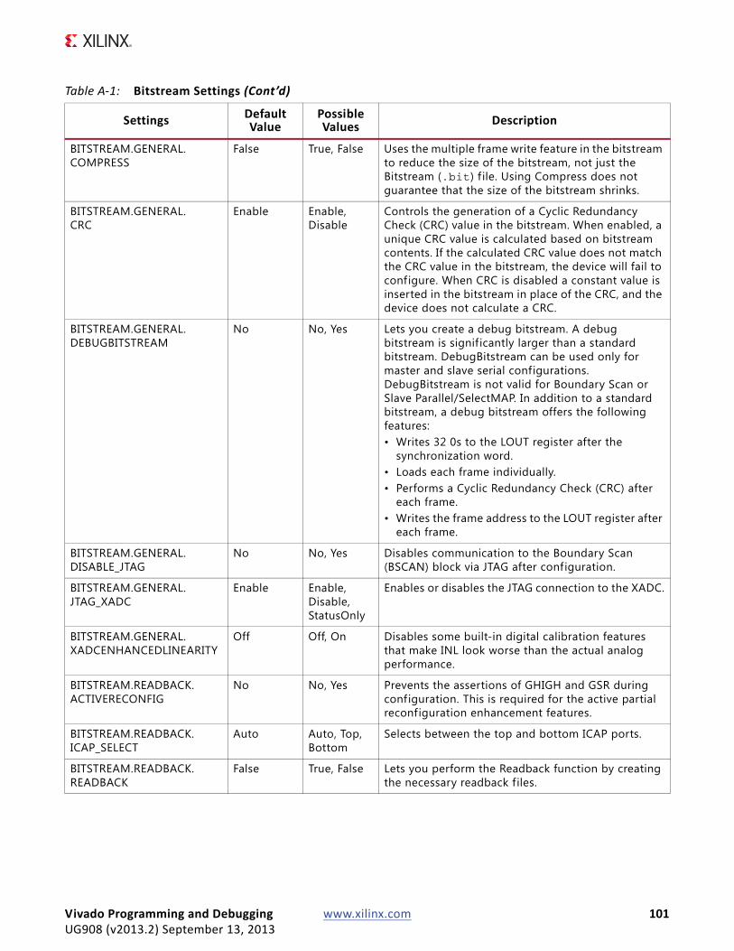
BITSTREAM.GENERAL.COMPRESS
False True, False Uses the multiple frame write feature in the bitstream to reduce the size of the bitstream, not just the Bitstream (.bit) f ile. Using Compress does not guarantee that the size of the bitstream shrinks.
BITSTREAM.GENERAL.CRC
Enable Enable, Disable
Controls the generation of a Cyclic Redundancy Check (CRC) value in the bitstream. When enabled, a unique CRC value is calculated based on bitstream contents. If the calculated CRC value does not match the CRC value in the bitstream, the device will fail to configure. When CRC is disabled a constant value is inserted in the bitstream in place of the CRC, and the device does not calculate a CRC.
BITSTREAM.GENERAL.DEBUGBITSTREAM
No No, Yes Lets you create a debug bitstream. A debug bitstream is significantly larger than a standard bitstream. DebugBitstream can be used only for master and slave serial configurations. DebugBitstream is not valid for Boundary Scan or Slave Parallel/SelectMAP. In addition to a standard bitstream, a debug bitstream offers the following features: • Writes 32 0s to the LOUT register after the
synchronization word.• Loads each frame individually.• Performs a Cyclic Redundancy Check (CRC) after
each frame.• Writes the frame address to the LOUT register after
each frame.
BITSTREAM.GENERAL.DISABLE_JTAG
No No, Yes Disables communication to the Boundary Scan (BSCAN) block via JTAG after configuration.
BITSTREAM.GENERAL.JTAG_XADC
Enable Enable, Disable, StatusOnly
Enables or disables the JTAG connection to the XADC.
BITSTREAM.GENERAL.XADCENHANCEDLINEARITY
Off Off, On Disables some built-in digital calibration features that make INL look worse than the actual analog performance.
BITSTREAM.READBACK.ACTIVERECONFIG
No No, Yes Prevents the assertions of GHIGH and GSR during configuration. This is required for the active partial reconfiguration enhancement features.
BITSTREAM.READBACK.ICAP_SELECT
Auto Auto, Top, Bottom
Selects between the top and bottom ICAP ports.
BITSTREAM.READBACK.READBACK
False True, False Lets you perform the Readback function by creating the necessary readback files.
Table A-1: Bitstream Settings (Cont’d)
Settings Default Value
Possible Values Description
Vivado Programming and Debugging www.xilinx.com 101UG908 (v2013.2) September 13, 2013
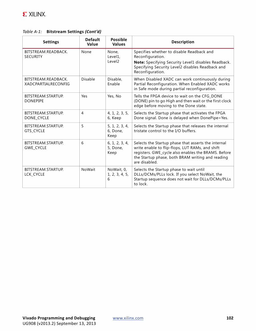
BITSTREAM.READBACK.SECURITY
None None, Level1, Level2
Specifies whether to disable Readback and Reconfiguration. Note: Specifying Security Level1 disables Readback. Specifying Security Level2 disables Readback and Reconfiguration.
BITSTREAM.READBACK.XADCPARTIALRECONFIG
Disable Disable, Enable
When Disabled XADC can work continuously during Partial Reconfiguration. When Enabled XADC works in Safe mode during partial reconfiguration.
BITSTREAM.STARTUP.DONEPIPE
Yes Yes, No Tells the FPGA device to wait on the CFG_DONE (DONE) pin to go High and then wait or the first clock edge before moving to the Done state.
BITSTREAM.STARTUP.DONE_CYCLE
4 4, 1, 2, 3, 5, 6, Keep
Selects the Startup phase that activates the FPGA Done signal. Done is delayed when DonePipe=Yes.
BITSTREAM.STARTUP.GTS_CYCLE
5 5, 1, 2, 3, 4, 6, Done, Keep
Selects the Startup phase that releases the internal tristate control to the I/O buffers.
BITSTREAM.STARTUP.GWE_CYCLE
6 6, 1, 2, 3, 4, 5, Done, Keep
Selects the Startup phase that asserts the internal write enable to flip-flops, LUT RAMs, and shift registers. GWE_cycle also enables the BRAMS. Before the Startup phase, both BRAM writing and reading are disabled.
BITSTREAM.STARTUP.LCK_CYCLE
NoWait NoWait, 0, 1, 2, 3, 4, 5, 6
Selects the Startup phase to wait until DLLs/DCMs/PLLs lock. If you select NoWait, the Startup sequence does not wait for DLLs/DCMs/PLLs to lock.
Table A-1: Bitstream Settings (Cont’d)
Settings Default Value
Possible Values Description
Vivado Programming and Debugging www.xilinx.com 102UG908 (v2013.2) September 13, 2013
.
BITSTREAM.STARTUP.MATCH_CYCLE
Auto Auto, NoWait, 0, 1, 2, 3, 4, 5, 6
Specifies a stall in the Startup cycle until digitally controlled impedance (DCI) match signals are asserted. DCI matching does not begin on the Match_cycle that was set in BitGen. The Startup sequence waits in this cycle until DCI has matched. Given that there are a number of variables in determining how long it takes DCI to match, the number of CCLK cycles required to complete the Startup sequence may vary in any given system. Ideally, the configuration solution should continue driving CCLK until DONE goes high.Note: When the Auto setting is specified, write_bitstream searches the design for any DCI I/O standards. If DCI standards exist, write_bitstream uses BITSTREAM.STARTUP.MATCH_CYCLE=2. Otherwise, write_bitstream uses BITSTREAM.STARTUP.MATCH_CYCLE=NoWait.
BITSTREAM.STARTUP.STARTUPCLK
Cclk Cclk, UserClk, JtagClk
The StartupClk sequence following the configuration of a device can be synchronized to either Cclk, a User Clock, or the JTAG Clock. The default is Cclk.• Cclk lets you synchronize to an internal clock
provided in the FPGA device.• UserClk lets you synchronize to a user-defined
signal connected to the CLK pin of the STARTUP symbol.
• JtagClk lets you synchronize to the clock provided by JTAG. This clock sequences the TAP controller which provides the control logic for JTAG.
Table A-1: Bitstream Settings (Cont’d)
Settings Default Value
Possible Values Description
Vivado Programming and Debugging www.xilinx.com 103UG908 (v2013.2) September 13, 2013
Appendix B
Additional Resources
Xilinx ResourcesFor support resources such as Answers, Documentation, Downloads, and Forums, see the Xilinx Support website at:
www.xilinx.com/support.
For a glossary of technical terms used in Xilinx documentation, see:
www.xilinx.com/company/terms.htm.
Solution CentersSee the Xilinx Solution Centers for support on devices, software tools, and intellectual property at all stages of the design cycle. Topics include design assistance, advisories, and troubleshooting tips.
ReferencesThese documents provide supplemental material useful with this guide:
Vivado Design Suite 2013.2 Documentation (http://www.xilinx.com/cgi-bin/docs/rdoc?v=2013.2;t=vivado+docs)
1. Vivado Design Suite User Guide: Logic Simulation (UG900)
2. Vivado Design Suite User Guide: Synthesis (UG901)
3. Vivado Design Suite User Guide: Implementation (UG904)
4. Vivado Design Suite: Release Notes, Installation and Licensing (UG973)
5. Vivado Design Suite User Guide: Design Flows Overview (UG892)
Vivado Programming and Debugging www.xilinx.com 104UG908 (v2013.2) September 13, 2013
References
ISE Design Suite 14.6 Documentation
6. iMPACT Help (http://www.xilinx.com/cgi-bin/docs/rdoc?l=en;v=14.6;d=isehelp_start.htm;a=pim_c_overview.htm)
Xilinx IP Documentation
7. LogiCORE IP ChipScope Pro Integrated Logic Analyzer (ILA) (v2) Datasheet (DS875)
8. LogiCORE IP Virtual Input/Output (VIO) v2.0 Product Guide (PG159)
9. LogiCORE IP IBERT for 7 Series GTX Transceivers (PG132)
10. LogiCORE IP IBERT for 7 Series GTP Transceivers (PG133)
11. LogiCORE IP IBERT for 7 Series GTH Transceivers (PG152)
Vivado Programming and Debugging www.xilinx.com 105UG908 (v2013.2) September 13, 2013


![Vivado Design Suite User Guide - Xilinx - All … the Vivado Design Suite User Guide: Programming and Debugging (UG908) [Ref 7] for information related to Chapter 6, Using the ILA](https://img.dokumen.tips/doc/110x75/5b1a14207f8b9a46258d0db5/vivado-design-suite-user-guide-xilinx-all-the-vivado-design-suite-user-guide.jpg)