Embed Size (px)
Citation preview

Vivado Design Suite User Guide
Power Analysis and Optimization
UG907 (v2018.1) April 4, 2018
Power Analysis and Optimization www.xilinx.com 2UG907 (v2018.1) April 4, 2018
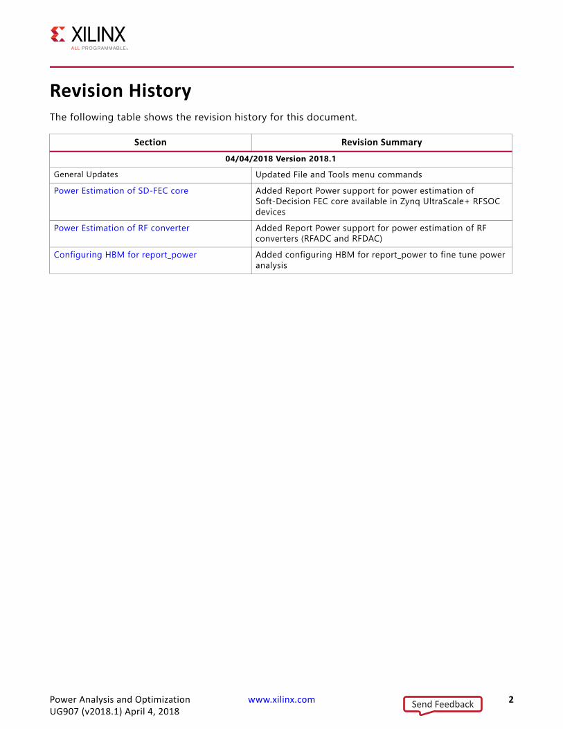
Revision HistoryThe following table shows the revision history for this document.
Section Revision Summary04/04/2018 Version 2018.1
General Updates Updated File and Tools menu commandsPower Estimation of SD-FEC core Added Report Power support for power estimation of
Soft-Decision FEC core available in Zynq UltraScale+ RFSOC devices
Power Estimation of RF converter Added Report Power support for power estimation of RF converters (RFADC and RFDAC)
Configuring HBM for report_power Added configuring HBM for report_power to fine tune power analysis
Send Feedback
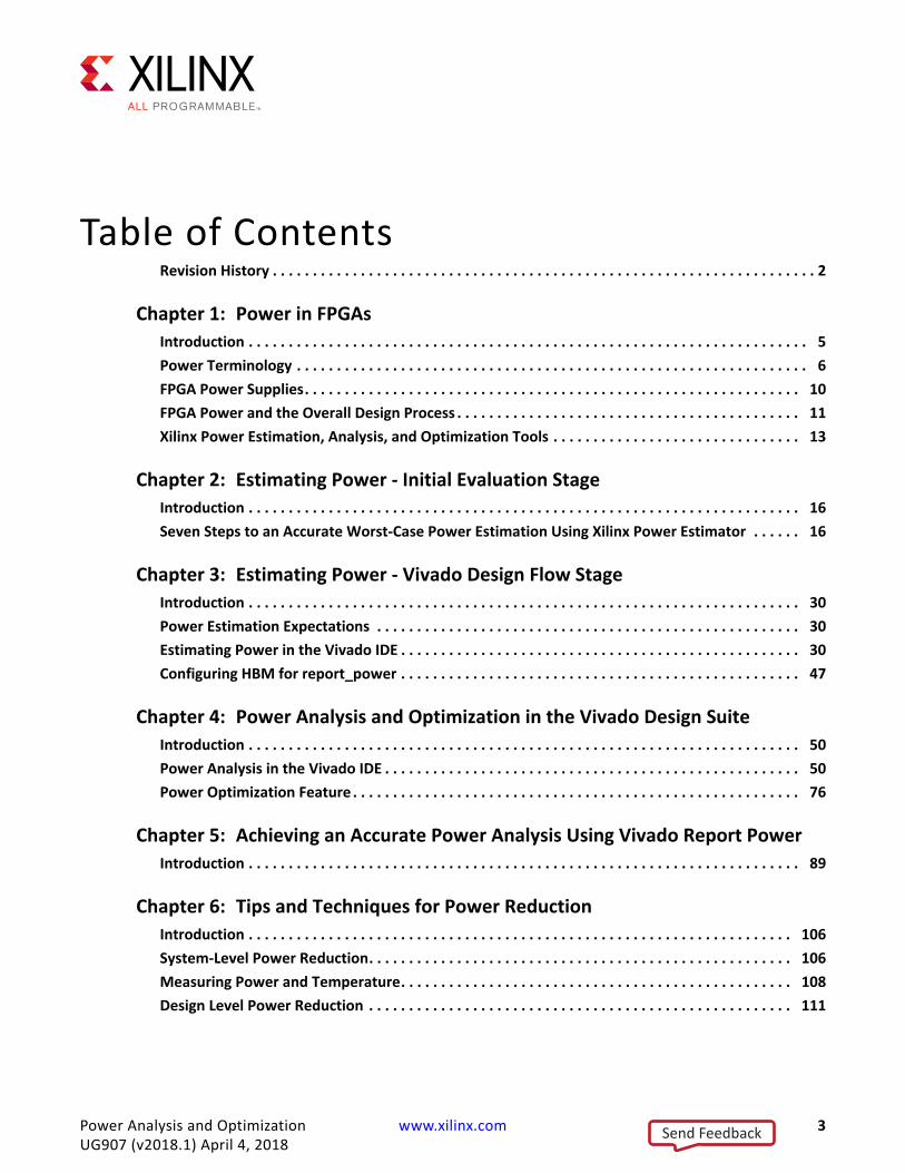
Table of ContentsRevision History . . . . . . . . . . . . . . . . . . . . . . . . . . . . . . . . . . . . . . . . . . . . . . . . . . . . . . . . . . . . . . . . . . . . 2
Chapter 1: Power in FPGAsIntroduction . . . . . . . . . . . . . . . . . . . . . . . . . . . . . . . . . . . . . . . . . . . . . . . . . . . . . . . . . . . . . . . . . . . . . . 5Power Terminology . . . . . . . . . . . . . . . . . . . . . . . . . . . . . . . . . . . . . . . . . . . . . . . . . . . . . . . . . . . . . . . . 6FPGA Power Supplies. . . . . . . . . . . . . . . . . . . . . . . . . . . . . . . . . . . . . . . . . . . . . . . . . . . . . . . . . . . . . . 10FPGA Power and the Overall Design Process . . . . . . . . . . . . . . . . . . . . . . . . . . . . . . . . . . . . . . . . . . . 11Xilinx Power Estimation, Analysis, and Optimization Tools . . . . . . . . . . . . . . . . . . . . . . . . . . . . . . . 13
Chapter 2: Estimating Power - Initial Evaluation StageIntroduction . . . . . . . . . . . . . . . . . . . . . . . . . . . . . . . . . . . . . . . . . . . . . . . . . . . . . . . . . . . . . . . . . . . . . 16Seven Steps to an Accurate Worst-Case Power Estimation Using Xilinx Power Estimator . . . . . . 16
Chapter 3: Estimating Power - Vivado Design Flow StageIntroduction . . . . . . . . . . . . . . . . . . . . . . . . . . . . . . . . . . . . . . . . . . . . . . . . . . . . . . . . . . . . . . . . . . . . . 30Power Estimation Expectations . . . . . . . . . . . . . . . . . . . . . . . . . . . . . . . . . . . . . . . . . . . . . . . . . . . . . 30Estimating Power in the Vivado IDE . . . . . . . . . . . . . . . . . . . . . . . . . . . . . . . . . . . . . . . . . . . . . . . . . . 30Configuring HBM for report_power . . . . . . . . . . . . . . . . . . . . . . . . . . . . . . . . . . . . . . . . . . . . . . . . . . 47
Chapter 4: Power Analysis and Optimization in the Vivado Design SuiteIntroduction . . . . . . . . . . . . . . . . . . . . . . . . . . . . . . . . . . . . . . . . . . . . . . . . . . . . . . . . . . . . . . . . . . . . . 50Power Analysis in the Vivado IDE . . . . . . . . . . . . . . . . . . . . . . . . . . . . . . . . . . . . . . . . . . . . . . . . . . . . 50Power Optimization Feature . . . . . . . . . . . . . . . . . . . . . . . . . . . . . . . . . . . . . . . . . . . . . . . . . . . . . . . . 76
Chapter 5: Achieving an Accurate Power Analysis Using Vivado Report PowerIntroduction . . . . . . . . . . . . . . . . . . . . . . . . . . . . . . . . . . . . . . . . . . . . . . . . . . . . . . . . . . . . . . . . . . . . . 89
Chapter 6: Tips and Techniques for Power ReductionIntroduction . . . . . . . . . . . . . . . . . . . . . . . . . . . . . . . . . . . . . . . . . . . . . . . . . . . . . . . . . . . . . . . . . . . . 106System-Level Power Reduction. . . . . . . . . . . . . . . . . . . . . . . . . . . . . . . . . . . . . . . . . . . . . . . . . . . . . 106Measuring Power and Temperature. . . . . . . . . . . . . . . . . . . . . . . . . . . . . . . . . . . . . . . . . . . . . . . . . 108Design Level Power Reduction . . . . . . . . . . . . . . . . . . . . . . . . . . . . . . . . . . . . . . . . . . . . . . . . . . . . . 111
Power Analysis and Optimization www.xilinx.com 3UG907 (v2018.1) April 4, 2018
Send Feedback

Appendix A: Additional Resources and Legal NoticesXilinx Resources . . . . . . . . . . . . . . . . . . . . . . . . . . . . . . . . . . . . . . . . . . . . . . . . . . . . . . . . . . . . . . . . . 118Solution Centers. . . . . . . . . . . . . . . . . . . . . . . . . . . . . . . . . . . . . . . . . . . . . . . . . . . . . . . . . . . . . . . . . 118Documentation Navigator and Design Hubs . . . . . . . . . . . . . . . . . . . . . . . . . . . . . . . . . . . . . . . . . . 118References . . . . . . . . . . . . . . . . . . . . . . . . . . . . . . . . . . . . . . . . . . . . . . . . . . . . . . . . . . . . . . . . . . . . . 119Training Resources. . . . . . . . . . . . . . . . . . . . . . . . . . . . . . . . . . . . . . . . . . . . . . . . . . . . . . . . . . . . . . . 119Please Read: Important Legal Notices . . . . . . . . . . . . . . . . . . . . . . . . . . . . . . . . . . . . . . . . . . . . . . . 119
Power Analysis and Optimization www.xilinx.com 4UG907 (v2018.1) April 4, 2018
Send Feedback
Chapter 1
Power in FPGAs
IntroductionThis chapter provides the terminology used in describing power when implementing an FPGA on a board. It also puts the FPGA development in the greater context of the system being designed and provides a high level description of what to expect at each stage of the design flow. The chapter then describes the Xilinx® tools used for power estimation, analysis, and optimization.
VIDEO: The Vivado Design Suite QuickTake Video Tutorial: Power Estimation and Analysis Using Vivado shows how Vivado can help you to estimate power consumption in your design and reviews best practices for getting the most accurate estimation.
VIDEO: The Vivado Design Suite QuickTake Video Tutorial: Power Optimization Using Vivado describes the factors that affect power consumption in an FPGA and how Vivado helps to minimize power consumption in your design, and looks at some advanced control and best practices for getting the most out of Vivado power optimization.
Power Analysis and Optimization www.xilinx.com 5UG907 (v2018.1) April 4, 2018
Send Feedback
Chapter 1: Power in FPGAs
Power TerminologyThe following terminology is used in this guide.
Device Static PowerDevice static power is the power from transistor leakage on all connected voltage rails and the circuits required for the FPGA to operate normally, post configuration. This is normally measured by programing a blank bitstream into the device. Device static power is a function of process, voltage, and temperature. This represents the steady state, intrinsic leakage in the device.
Design PowerDesign power is the dynamic power of the user design, due to the input data pattern and the design internal activity. This power is instantaneous and varies at each clock cycle. It depends on voltage levels and logic and routing resources used. This also includes static current from I/O terminations, clock managers, and other circuits that need power when used. It does not include power supplied to off-chip devices.
Total On-Chip PowerTotal on-chip power is the power consumed internally within the FPGA, equal to the sum of device static power and design power. It is also known as thermal power.
Off-Chip PowerOff-chip power is the current that flows from the supply source through the FPGA power pins, then out of the I/Os and dissipated in external board components. The currents supplied by the FPGA are generally consumed in off-chip components such as I/O terminations, LEDs, or the I/O buffers of other chips, and therefore do not raise the device junction temperature.
Note: Negative off-chip power dissipated is the power that is sourced from external source and dissipated inside our device.
Power-On CurrentPower-on current is transient current that occurs when power is first applied to the FPGA. This current varies for each voltage supply and depends on the FPGA construction as well as the ability of the power supply source to ramp up to the nominal voltage. This current also depends on the device's operating conditions, such as temperature and sequencing between the different supplies. Power-on current is generally lower than operating current due to architectural enhancements as well as adherence to proper power-on sequencing.
Power Analysis and Optimization www.xilinx.com 6UG907 (v2018.1) April 4, 2018
Send Feedback

Chapter 1: Power in FPGAs
Junction Temperature (°C)Junction temperature is the temperature of the device in operation. Typically when selecting the device, you choose a temperature grade. This grade defines a temperature range in which Xilinx® guarantees that the device will operate as specified. If your operating conditions are above the Grade Maximum, but remain below the Absolute Maximum temperature, then the device operation is no longer guaranteed. Exceeding the Absolute Maximum operating conditions may damage the device.
Junction Temperature = Ambient Temperature + Total On-Chip Power * Effective Thermal Resistance to Air (ΘJA)
Ambient Temperature (°C)Ambient temperature is the temperature of the air immediately surrounding the device under the expected system operating conditions.
Effective Thermal Resistance to Air (ΘJA (°C/W))Effective thermal resistance to air is also known as Theta-JA, and TJA. This coefficient defines how power is dissipated from the FPGA silicon to the environment (device junction to ambient air). It includes contributions from all elements, from the silicon chip dimensions to the surrounding air, plus any material in between, such as the package, the PCB, any heat sink, and airflow. Typically this combines thermal resistance and interdependencies from the two main paths by which the generated heat can escape onto the environment:
• Upward from the die to the air (junction to air or ΘJA),• Downward from the die through the board and into the air (junction to board or ΘJB).
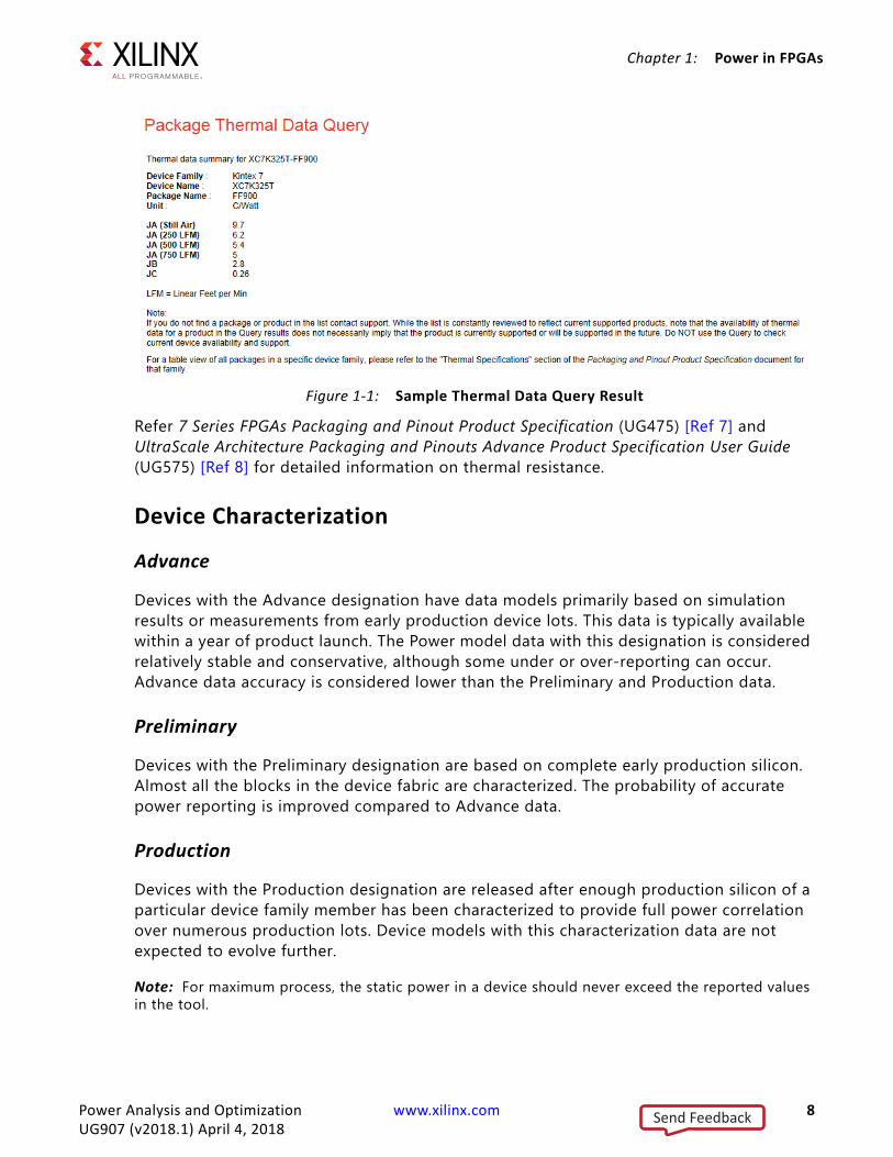
Thermal data for Xilinx device packages can be found using the Package Thermal Data Query tool.
A sample Thermal Data Query result is shown in Figure 1-1.
Power Analysis and Optimization www.xilinx.com 7UG907 (v2018.1) April 4, 2018
Send Feedback
Chapter 1: Power in FPGAs
Refer 7 Series FPGAs Packaging and Pinout Product Specification (UG475) [Ref 7] and UltraScale Architecture Packaging and Pinouts Advance Product Specification User Guide (UG575) [Ref 8] for detailed information on thermal resistance.
Device Characterization
Advance
Devices with the Advance designation have data models primarily based on simulation results or measurements from early production device lots. This data is typically available within a year of product launch. The Power model data with this designation is considered relatively stable and conservative, although some under or over-reporting can occur. Advance data accuracy is considered lower than the Preliminary and Production data.
Preliminary
Devices with the Preliminary designation are based on complete early production silicon. Almost all the blocks in the device fabric are characterized. The probability of accurate power reporting is improved compared to Advance data.
Production
Devices with the Production designation are released after enough production silicon of a particular device family member has been characterized to provide full power correlation over numerous production lots. Device models with this characterization data are not expected to evolve further.
Note: For maximum process, the static power in a device should never exceed the reported values in the tool.
X-Ref Target - Figure 1-1
Figure 1-1: Sample Thermal Data Query Result
Power Analysis and Optimization www.xilinx.com 8UG907 (v2018.1) April 4, 2018
Send Feedback

Chapter 1: Power in FPGAs
Signal RateSignal rate is the number of times an element changes state (high-to-low and low-to-high) per second. Xilinx tools express this as millions of transitions per seconds (Mtr/s). For example, if a signal changes at every four clocks cycle with respect to a 100MHz (10ns) Clock, then the Signal Rate is: 1/(4*10ns) = 25 Mtr/s.
Toggle RateToggle rate (%) is the rate at which the output of a synchronous logic element switches compared to a given clock input. It is modeled as a percentage between 0 - 100%. A toggle rate of 100% means that on average the output toggles once during every clock cycle. As an example, If a signal changes at every four clock cycles with respect to a Clock of any frequency, then the Toggle Rate is: (1/4)*100 = 25%.
IMPORTANT: The toggle rate for clock nets is always 200%, which means that the net toggles twice in a cycle.
TIP: Ideally a synchronous net changes once per clock (except DDR nets); thus the maximum toggle rate is 100%. If a synchronous net is prone to glitches, use Signal Rate to specify the switching activity.
For asynchronous elements such as nets and logic that are not synchronized with a clock, the toggle rate cannot be computed. The Vivado® power tools expect the use of Signal Rate for these kinds of elements.
For example: By default the primary inputs of the design are not associated with a specific clock. Use the set_input_delay constraint to associate a clock with the primary inputs. If you do not associate a clock, the power tools compute the toggle rate with respect to either the capturing clock or the fastest clock in the design.
Static ProbabilityStatic probability defines the relative time of the analysis duration during which the considered element is driven at a high (1’b1) logic level and the valid range is 0 to 1. As an example, if a signal is at Logic 1 for 40ns in a duration of 100ns, the static probability = 40/100 = 0.4.
TIP: Static Probability = 1 represents that the considered element is held at Logic 1 throughout the analysis duration and never toggles (toggle/signal rate = 0).
Similarly, Static Probability=0 represents that the considered element is held at Logic 0 throughout the analysis duration and never toggles (toggle/signal rate =0).
Power Analysis and Optimization www.xilinx.com 9UG907 (v2018.1) April 4, 2018
Send Feedback
Chapter 1: Power in FPGAs
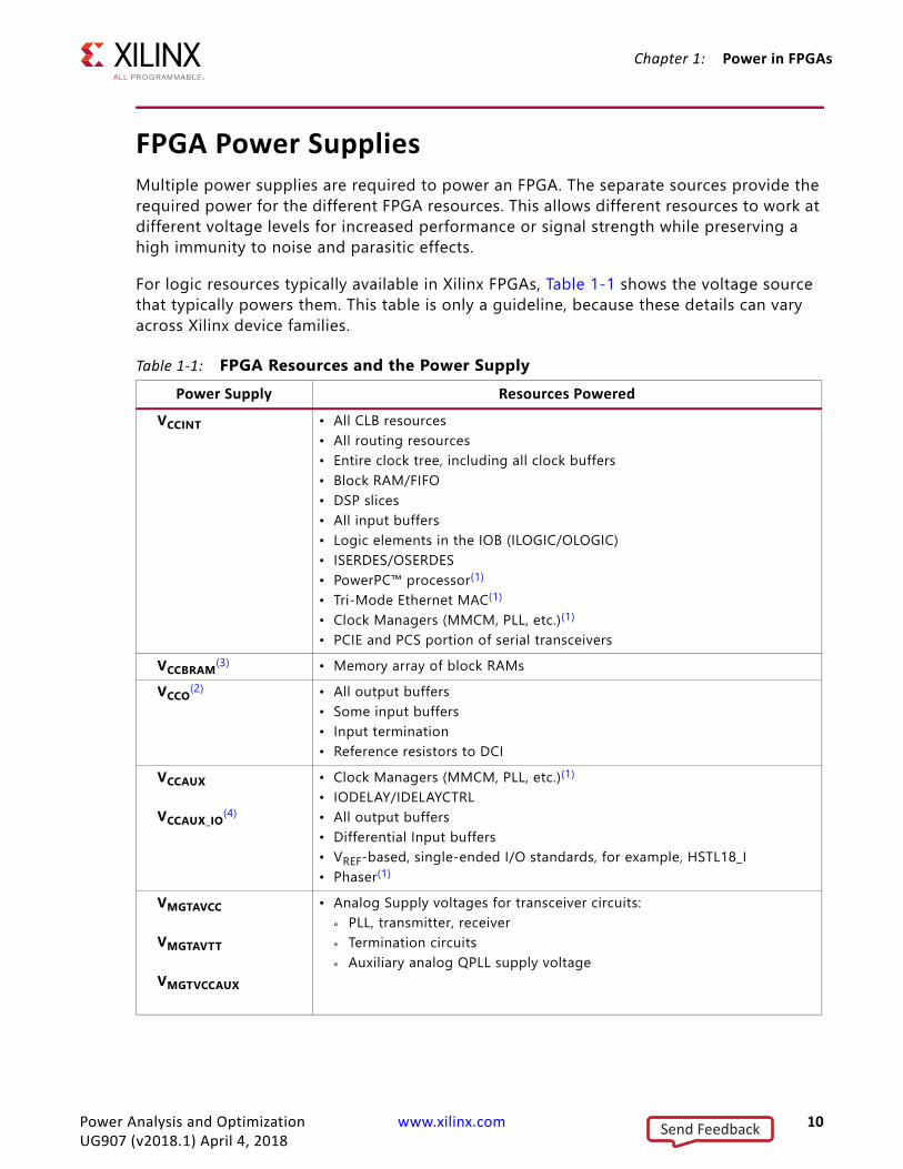
FPGA Power SuppliesMultiple power supplies are required to power an FPGA. The separate sources provide the required power for the different FPGA resources. This allows different resources to work at different voltage levels for increased performance or signal strength while preserving a high immunity to noise and parasitic effects.
For logic resources typically available in Xilinx FPGAs, Table 1-1 shows the voltage source that typically powers them. This table is only a guideline, because these details can vary across Xilinx device families.
Table 1-1: FPGA Resources and the Power SupplyPower Supply Resources Powered
VCCINT • All CLB resources• All routing resources• Entire clock tree, including all clock buffers• Block RAM/FIFO• DSP slices• All input buffers• Logic elements in the IOB (ILOGIC/OLOGIC)• ISERDES/OSERDES• PowerPC™ processor(1)
• Tri-Mode Ethernet MAC(1)
• Clock Managers (MMCM, PLL, etc.)(1)
• PCIE and PCS portion of serial transceiversVCCBRAM(3) • Memory array of block RAMsVCCO(2) • All output buffers
• Some input buffers• Input termination• Reference resistors to DCI
VCCAUX
VCCAUX_IO(4)
• Clock Managers (MMCM, PLL, etc.)(1)
• IODELAY/IDELAYCTRL• All output buffers• Differential Input buffers• VREF-based, single-ended I/O standards, for example, HSTL18_I• Phaser(1)
VMGTAVCC
VMGTAVTT
VMGTVCCAUX
• Analog Supply voltages for transceiver circuits:° PLL, transmitter, receiver° Termination circuits° Auxiliary analog QPLL supply voltage
Power Analysis and Optimization www.xilinx.com 10UG907 (v2018.1) April 4, 2018
Send Feedback
Chapter 1: Power in FPGAs
FPGA Power and the Overall Design ProcessFrom project conception to completion there are many different factors to consider that influence power. Omitting for a moment all other constraints (functionality, performance, cost, and time to market), power related tasks can be sorted into two separate classes.• Physical domain
Enclosure, board shape, power supply and power distribution network (PDN), thermal power dissipation system.
VCCPINT
VCCPAUX
VCCPLL
VCCO_DDR
VCCO_MIO
• Zynq®-7000 AP SoC:° Processor° Memory° I/O° Peripherals° AXI Interfaces
VCC_PSINTFP
VCC_PSINTLP
VCC_PSAUX
VCCPSINTFP_DDR
VCC_PSPLL
VPS_MGTRAVCC
VPS_MGTRAVTT
VCCO_PSDDR
VCCO_PSDDR_PLL
VCCO_PSIO
VCCINT_VCU
• Zynq-UltraScale+ MPSoC° Processor° Memory° I/O° Peripherals
Notes: 1. These resources are available only in certain device families. Refer to the appropriate data sheets and user guides
for more information.2. VCCO in bank 0 (VCCO_0 or VCCO_CONFIG) powers all I/Os in bank 0 as well as the configuration circuitry. See the
applicable Configuration User Guide.3. Xilinx 7 series Block RAM/FIFO only.4. Xilinx 7 series High Performance (HP) I/O banks only.
Table 1-1: FPGA Resources and the Power Supply (Cont’d)
Power Supply Resources Powered
Power Analysis and Optimization www.xilinx.com 11UG907 (v2018.1) April 4, 2018
Send Feedback
Chapter 1: Power in FPGAs
• Functional domain
Area, performance, I/O interfaces signal integrity.
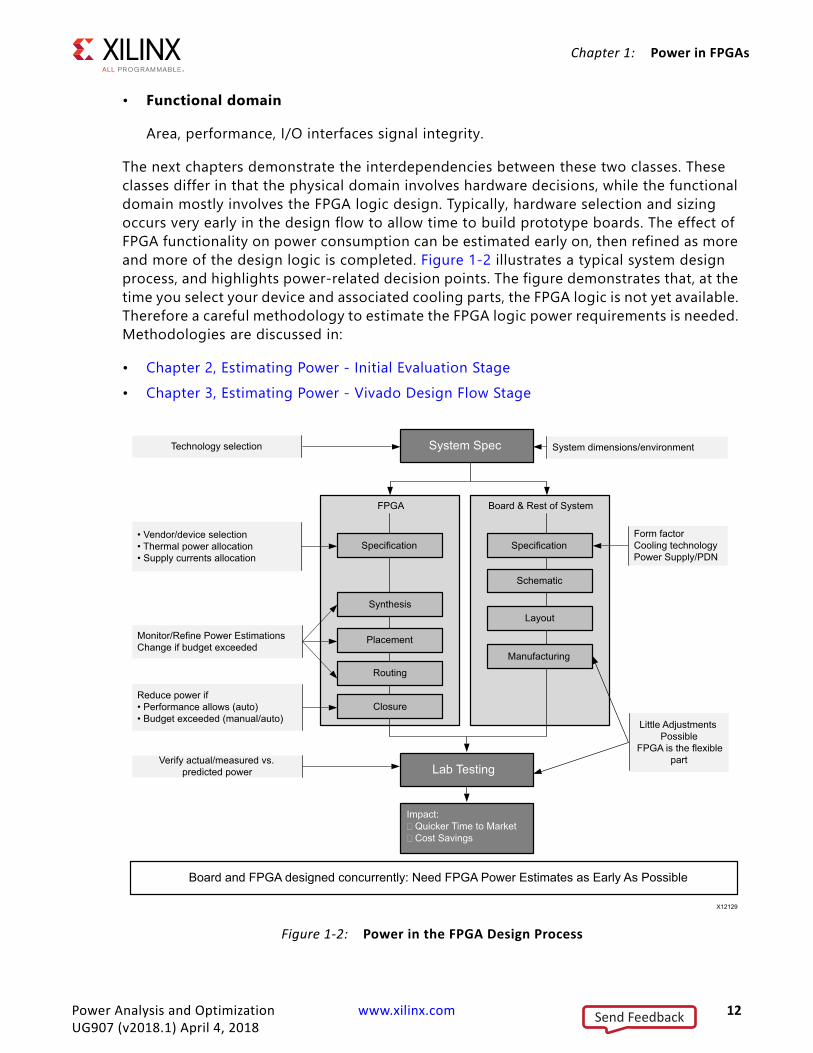
The next chapters demonstrate the interdependencies between these two classes. These classes differ in that the physical domain involves hardware decisions, while the functional domain mostly involves the FPGA logic design. Typically, hardware selection and sizing occurs very early in the design flow to allow time to build prototype boards. The effect of FPGA functionality on power consumption can be estimated early on, then refined as more and more of the design logic is completed. Figure 1-2 illustrates a typical system design process, and highlights power-related decision points. The figure demonstrates that, at the time you select your device and associated cooling parts, the FPGA logic is not yet available. Therefore a careful methodology to estimate the FPGA logic power requirements is needed. Methodologies are discussed in:
• Chapter 2, Estimating Power - Initial Evaluation Stage• Chapter 3, Estimating Power - Vivado Design Flow Stage X-Ref Target - Figure 1-2
Figure 1-2: Power in the FPGA Design Process
X12129
System Spec
FPGA Board & Rest of System
Technology selection
• Vendor/device selection• Thermal power allocation• Supply currents allocation
Monitor/Refine Power EstimationsChange if budget exceeded
System dimensions/environment
Reduce power if• Performance allows (auto)• Budget exceeded (manual/auto)
Lab Testing
Impact:� Quicker Time to Market� Cost Savings
Form factorCooling technologyPower Supply/PDN
Verify actual/measured vs. predicted power
Little AdjustmentsPossible
FPGA is the flexible part
Board and FPGA designed concurrently: Need FPGA Power Estimates as Early As Possible
Specification
Synthesis
Placement
Routing
Closure
Specification
Layout
Manufacturing
Schematic
Power Analysis and Optimization www.xilinx.com 12UG907 (v2018.1) April 4, 2018
Send Feedback
Chapter 1: Power in FPGAs
The following chapters provide methodologies to analyze and reduce power consumption throughout the design process.
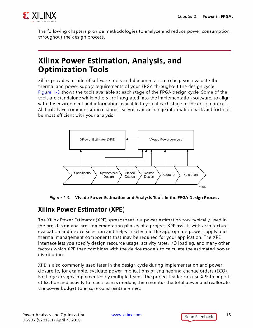
Xilinx Power Estimation, Analysis, and Optimization ToolsXilinx provides a suite of software tools and documentation to help you evaluate the thermal and power supply requirements of your FPGA throughout the design cycle. Figure 1-3 shows the tools available at each stage of the FPGA design cycle. Some of the tools are standalone while others are integrated into the implementation software, to align with the environment and information available to you at each stage of the design process. All tools have communication channels so you can exchange information back and forth to be most efficient with your analysis.
Xilinx Power Estimator (XPE)The Xilinx Power Estimator (XPE) spreadsheet is a power estimation tool typically used in the pre-design and pre-implementation phases of a project. XPE assists with architecture evaluation and device selection and helps in selecting the appropriate power supply and thermal management components that may be required for your application. The XPE interface lets you specify design resource usage, activity rates, I/O loading, and many other factors which XPE then combines with the device models to calculate the estimated power distribution.
XPE is also commonly used later in the design cycle during implementation and power closure to, for example, evaluate power implications of engineering change orders (ECO). For large designs implemented by multiple teams, the project leader can use XPE to import utilization and activity for each team's module, then monitor the total power and reallocate the power budget to ensure constraints are met.
X-Ref Target - Figure 1-3
Figure 1-3: Vivado Power Estimation and Analysis Tools in the FPGA Design Process
XPower Estimator (XPE) Vivado Power Analysis
X12986
Specification
SynthesizedDesign
PlacedDesign
RoutedDesign Closure Validation
Power Analysis and Optimization www.xilinx.com 13UG907 (v2018.1) April 4, 2018
Send Feedback
Chapter 1: Power in FPGAs
For more information on using the Xilinx Power Estimator (XPE), see Xilinx Power Estimator User Guide (UG440) [Ref 4].
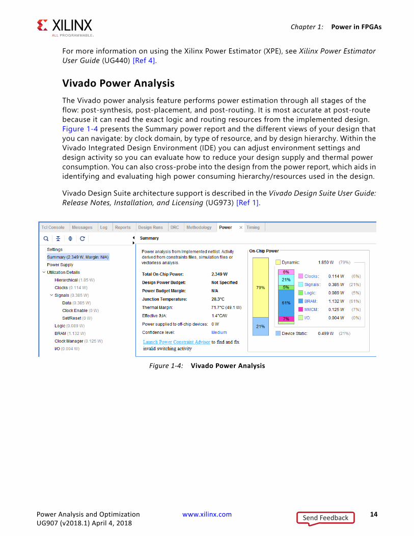
Vivado Power AnalysisThe Vivado power analysis feature performs power estimation through all stages of the flow: post-synthesis, post-placement, and post-routing. It is most accurate at post-route because it can read the exact logic and routing resources from the implemented design. Figure 1-4 presents the Summary power report and the different views of your design that you can navigate: by clock domain, by type of resource, and by design hierarchy. Within the Vivado Integrated Design Environment (IDE) you can adjust environment settings and design activity so you can evaluate how to reduce your design supply and thermal power consumption. You can also cross-probe into the design from the power report, which aids in identifying and evaluating high power consuming hierarchy/resources used in the design.
Vivado Design Suite architecture support is described in the Vivado Design Suite User Guide: Release Notes, Installation, and Licensing (UG973) [Ref 1].
X-Ref Target - Figure 1-4
Figure 1-4: Vivado Power Analysis
Power Analysis and Optimization www.xilinx.com 14UG907 (v2018.1) April 4, 2018
Send Feedback

Chapter 1: Power in FPGAs
Vivado Power OptimizationThe Vivado design tools offer a variety of power optimizations to minimize dynamic power consumption by up to 30% in your design. These optimizations use ASIC strength clock gating or advanced sequential clock gating or both techniques to minimize switching activity without affecting the design functionality. The power optimizations can be applied on the entire design or on selected portions of the design.
In Vivado, you can perform power optimization using the Vivado IDE or using Tcl commands.
X-Ref Target - Figure 1-5
Figure 1-5: Power Optimization Report in Vivado
Power Analysis and Optimization www.xilinx.com 15UG907 (v2018.1) April 4, 2018
Send Feedback

Chapter 2
Estimating Power - Initial Evaluation Stage
IntroductionThis chapter describes a methodology to evaluate your design's power consumption during the initial evaluation stage of the design cycle. You will work in Xilinx Power Estimator during this stage of the design cycle.
If you have already completed the initial evaluation stage, go to the next chapter, which describes a methodology to evaluate your design’s power consumption in the later stage of the design cycle. At this stage, you will use the Vivado® Design Suite, which automates and simplifies power estimation.
Seven Steps to an Accurate Worst-Case Power Estimation Using Xilinx Power EstimatorPower BudgetingAt this stage you have determined that an FPGA is the most effective technology for your application. Now you need to define which vendor, family, and package can best fit your functionality, performance, cost, and power budgets. In terms of power, you must estimate the total device power requirements even before any logic is developed. Understanding the total power requirements will help you define your power delivery and cooling system specifications.
Questions that you will typically ask yourself are:
• How many voltage supplies are needed?• How much power will each voltage supply draw?• How much of the absorbed energy will generate heat?
Power Analysis and Optimization www.xilinx.com 16UG907 (v2018.1) April 4, 2018
Send Feedback
Chapter 2: Estimating Power - Initial Evaluation Stage
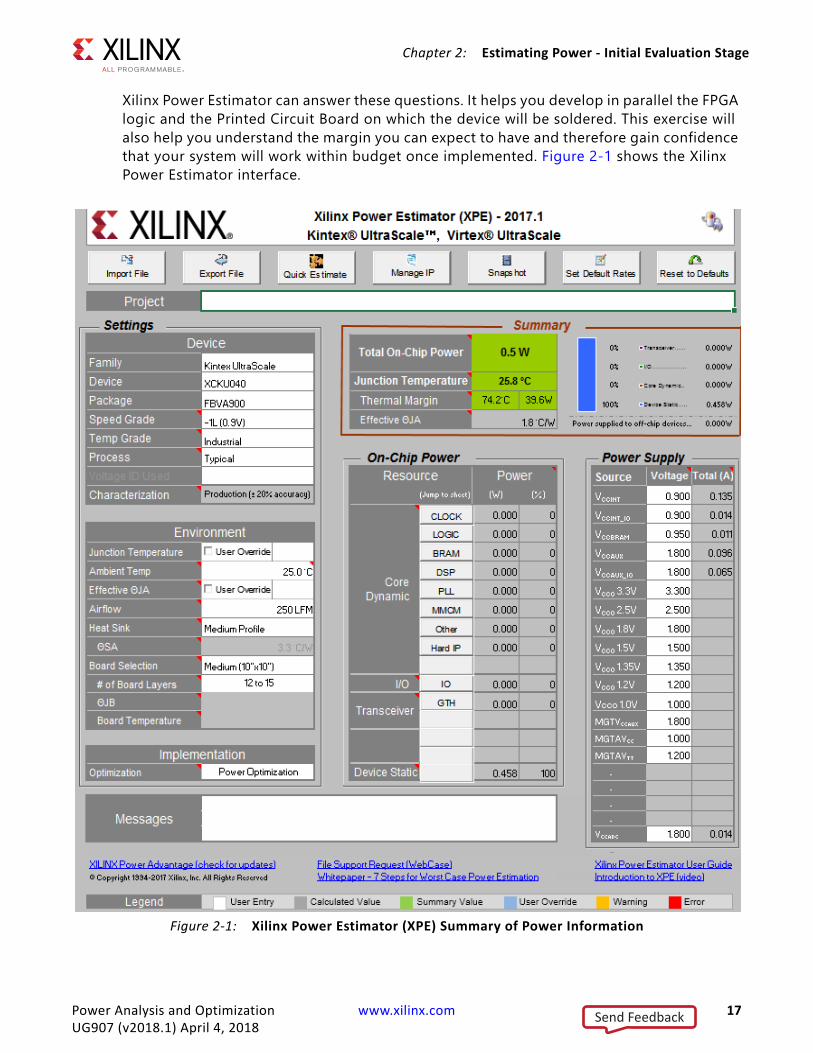
Xilinx Power Estimator can answer these questions. It helps you develop in parallel the FPGA logic and the Printed Circuit Board on which the device will be soldered. This exercise will also help you understand the margin you can expect to have and therefore gain confidence that your system will work within budget once implemented. Figure 2-1 shows the Xilinx Power Estimator interface.
X-Ref Target - Figure 2-1
Figure 2-1: Xilinx Power Estimator (XPE) Summary of Power Information
Power Analysis and Optimization www.xilinx.com 17UG907 (v2018.1) April 4, 2018
Send Feedback
Chapter 2: Estimating Power - Initial Evaluation Stage
Estimating Power in Xilinx Power Estimator (XPE)In any FPGA design, you must properly set power and cooling specifications in order to create a functioning and reliable system. In most cases, these thermal and power specifications must be set before PCB design. Because of the flexibility of FPGAs, often the FPGA design is not completed (or sometimes even started) before system design or PCB fabrication. This creates a challenge for FPGA designers, since thermal and power characteristics can vary dramatically depending on the bitstream (design), clocking, and data flow in the device.
Underdesigning the power or thermal system can make the FPGA operate out of specification. This can result in the FPGA not operating at the expected performance and can have other more serious consequences. Overdesigning the power system is generally less serious, but is still not desirable since it can add unnecessary cost and complexity to the overall FPGA design. The task of power estimation is not a trivial one before completing the design.
These steps are primarily focused on power analysis. There are several techniques for power optimization that can be explored and applied during the analysis and can result in significant power savings. Power Optimization techniques are discussed in the next chapter.
Step 1: Obtain the latest version of Xilinx Power Estimator for the selected target device.
It is important to make sure you are using the latest version of the Xilinx Power Estimator (XPE) tool because power information is updated periodically to reflect the latest power modeling and characterization data.
The latest version of XPE can be obtained from XPE Downloads web page on the Xilinx® web site. Check this web site occasionally during the design process to determine whether a new version has become available. If a new version is available, you can import the data from a previous version into the updated version using the Import File button on the updated version's Summary sheet. Keeping the Xilinx Power Estimator up to date ensures that the most current power information will be used in the power analysis at all times during the design cycle.
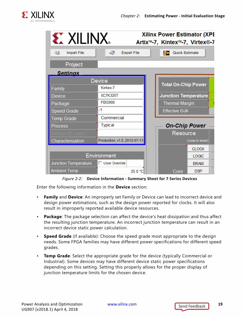
Step 2: Complete the Device information on the Summary sheet.
Make sure that each field in the Device section of the Summary sheet is properly set since each can have a significant effect on the end power calculation, particularly in static and clocking power (Figure 2-2).
Power Analysis and Optimization www.xilinx.com 18UG907 (v2018.1) April 4, 2018
Send Feedback
Chapter 2: Estimating Power - Initial Evaluation Stage
Enter the following information in the Device section:
• Family and Device: An improperly set Family or Device can lead to incorrect device and design power estimations, such as the design power reported for clocks. It will also result in improperly reported available device resources.
• Package: The package selection can affect the device's heat dissipation and thus affect the resulting junction temperature. An incorrect junction temperature can result in an incorrect device static power calculation.
• Speed Grade (if available): Choose the speed grade most appropriate to the design needs. Some FPGA families may have different power specifications for different speed grades.
• Temp Grade: Select the appropriate grade for the device (typically Commercial or Industrial). Some devices may have different device static power specifications depending on this setting. Setting this properly allows for the proper display of junction temperature limits for the chosen device.
X-Ref Target - Figure 2-2
Figure 2-2: Device Information - Summary Sheet for 7 Series Devices
Power Analysis and Optimization www.xilinx.com 19UG907 (v2018.1) April 4, 2018
Send Feedback

Chapter 2: Estimating Power - Initial Evaluation Stage
• Process: For the purposes of a worst-case analysis, the recommended process setting is Maximum. The default setting of Typical gives a closer picture to what would be measured statistically, but changing the setting to Maximum modifies the power specification to worst-case values.
• Voltage ID Used: The Voltage ID (VID) voltage is the minimum possible VCCINT voltage at which the FPGA can run and still meet its performance specifications. This voltage is tested when the FPGA is manufactured and the value is programmed into the DNA (device identifier) eFUSE register on the FPGA. Activating the VID feature in your design to operate the FPGA at this VID voltage can result in a significant static power savings over operating the FPGA at its nominal voltage.Note: This option applies to Virtex®-7, -1 speed grade, Commercial Temp grade, and Maximum Process FPGAs only.
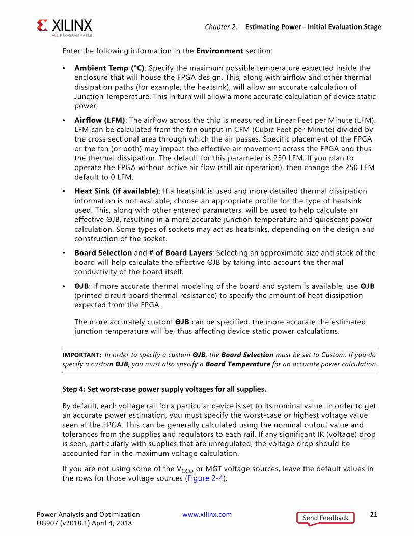
Step 3: Complete the Environment information on the Summary sheet.
Set the proper environment conditions in the Environment section of the Summary sheet (Figure 2-3).X-Ref Target - Figure 2-3
Figure 2-3: Environment Information - Summary Sheet for 7 Series Devices
Power Analysis and Optimization www.xilinx.com 20UG907 (v2018.1) April 4, 2018
Send Feedback
Chapter 2: Estimating Power - Initial Evaluation Stage
Enter the following information in the Environment section:
• Ambient Temp (°C): Specify the maximum possible temperature expected inside the enclosure that will house the FPGA design. This, along with airflow and other thermal dissipation paths (for example, the heatsink), will allow an accurate calculation of Junction Temperature. This in turn will allow a more accurate calculation of device static power.
• Airflow (LFM): The airflow across the chip is measured in Linear Feet per Minute (LFM). LFM can be calculated from the fan output in CFM (Cubic Feet per Minute) divided by the cross sectional area through which the air passes. Specific placement of the FPGA or the fan (or both) may impact the effective air movement across the FPGA and thus the thermal dissipation. The default for this parameter is 250 LFM. If you plan to operate the FPGA without active air flow (still air operation), then change the 250 LFM default to 0 LFM.
• Heat Sink (if available): If a heatsink is used and more detailed thermal dissipation information is not available, choose an appropriate profile for the type of heatsink used. This, along with other entered parameters, will be used to help calculate an effective ΘJB, resulting in a more accurate junction temperature and quiescent power calculation. Some types of sockets may act as heatsinks, depending on the design and construction of the socket.
• Board Selection and # of Board Layers: Selecting an approximate size and stack of the board will help calculate the effective ΘJB by taking into account the thermal conductivity of the board itself.
• ΘJB: If more accurate thermal modeling of the board and system is available, use ΘJB (printed circuit board thermal resistance) to specify the amount of heat dissipation expected from the FPGA.
The more accurately custom ΘJB can be specified, the more accurate the estimated junction temperature will be, thus affecting device static power calculations.
IMPORTANT: In order to specify a custom ΘJB, the Board Selection must be set to Custom. If you do specify a custom ΘJB, you must also specify a Board Temperature for an accurate power calculation.
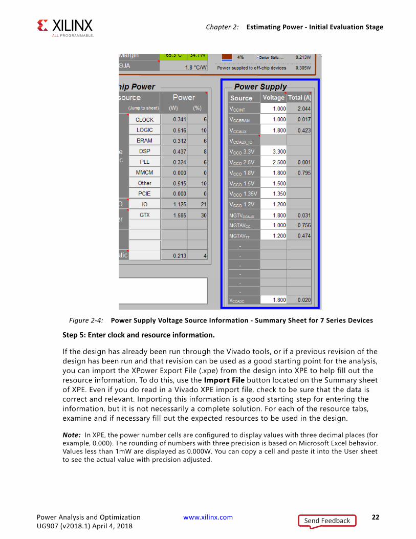
Step 4: Set worst-case power supply voltages for all supplies.
By default, each voltage rail for a particular device is set to its nominal value. In order to get an accurate power estimation, you must specify the worst-case or highest voltage value seen at the FPGA. This can be generally calculated using the nominal output value and tolerances from the supplies and regulators to each rail. If any significant IR (voltage) drop is seen, particularly with supplies that are unregulated, the voltage drop should be accounted for in the maximum voltage calculation.If you are not using some of the VCCO or MGT voltage sources, leave the default values in the rows for those voltage sources (Figure 2-4).
Power Analysis and Optimization www.xilinx.com 21UG907 (v2018.1) April 4, 2018
Send Feedback
Chapter 2: Estimating Power - Initial Evaluation Stage
Step 5: Enter clock and resource information.
If the design has already been run through the Vivado tools, or if a previous revision of the design has been run and that revision can be used as a good starting point for the analysis, you can import the XPower Export File (.xpe) from the design into XPE to help fill out the resource information. To do this, use the Import File button located on the Summary sheet of XPE. Even if you do read in a Vivado XPE import file, check to be sure that the data is correct and relevant. Importing this information is a good starting step for entering the information, but it is not necessarily a complete solution. For each of the resource tabs, examine and if necessary fill out the expected resources to be used in the design.
Note: In XPE, the power number cells are configured to display values with three decimal places (for example, 0.000). The rounding of numbers with three precision is based on Microsoft Excel behavior. Values less than 1mW are displayed as 0.000W. You can copy a cell and paste it into the User sheet to see the actual value with precision adjusted.
X-Ref Target - Figure 2-4
Figure 2-4: Power Supply Voltage Source Information - Summary Sheet for 7 Series Devices
Power Analysis and Optimization www.xilinx.com 22UG907 (v2018.1) April 4, 2018
Send Feedback
Chapter 2: Estimating Power - Initial Evaluation Stage
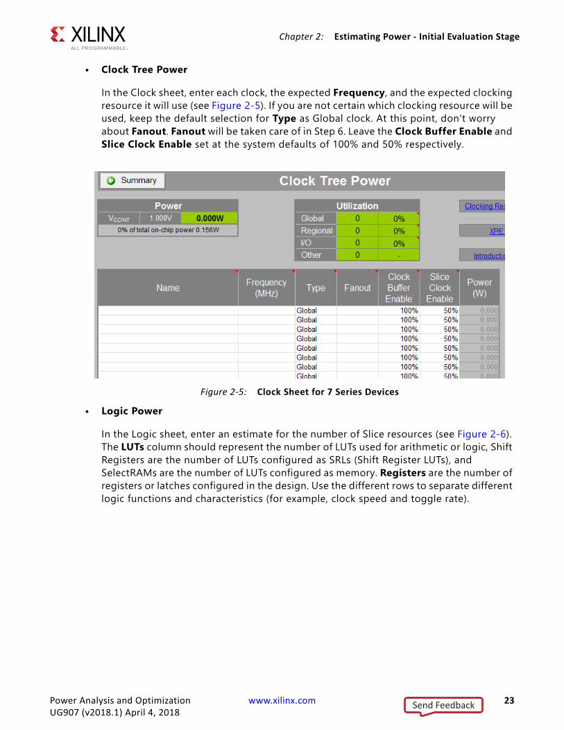
• Clock Tree Power
In the Clock sheet, enter each clock, the expected Frequency, and the expected clocking resource it will use (see Figure 2-5). If you are not certain which clocking resource will be used, keep the default selection for Type as Global clock. At this point, don't worry about Fanout. Fanout will be taken care of in Step 6. Leave the Clock Buffer Enable and Slice Clock Enable set at the system defaults of 100% and 50% respectively.
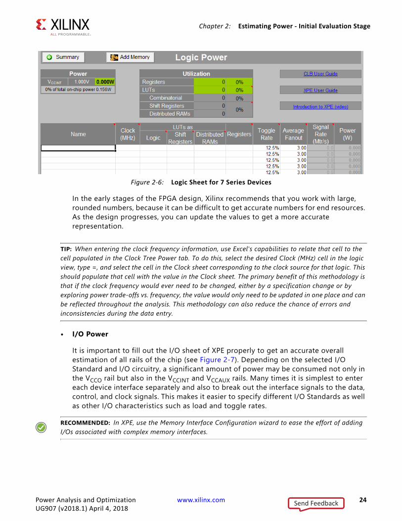
• Logic Power
In the Logic sheet, enter an estimate for the number of Slice resources (see Figure 2-6). The LUTs column should represent the number of LUTs used for arithmetic or logic, Shift Registers are the number of LUTs configured as SRLs (Shift Register LUTs), and SelectRAMs are the number of LUTs configured as memory. Registers are the number of registers or latches configured in the design. Use the different rows to separate different logic functions and characteristics (for example, clock speed and toggle rate).
X-Ref Target - Figure 2-5
Figure 2-5: Clock Sheet for 7 Series Devices
Power Analysis and Optimization www.xilinx.com 23UG907 (v2018.1) April 4, 2018
Send Feedback
Chapter 2: Estimating Power - Initial Evaluation Stage
In the early stages of the FPGA design, Xilinx recommends that you work with large, rounded numbers, because it can be difficult to get accurate numbers for end resources. As the design progresses, you can update the values to get a more accurate representation.
TIP: When entering the clock frequency information, use Excel's capabilities to relate that cell to the cell populated in the Clock Tree Power tab. To do this, select the desired Clock (MHz) cell in the logic view, type =, and select the cell in the Clock sheet corresponding to the clock source for that logic. This should populate that cell with the value in the Clock sheet. The primary benefit of this methodology is that if the clock frequency would ever need to be changed, either by a specification change or by exploring power trade-offs vs. frequency, the value would only need to be updated in one place and can be reflected throughout the analysis. This methodology can also reduce the chance of errors and inconsistencies during the data entry.
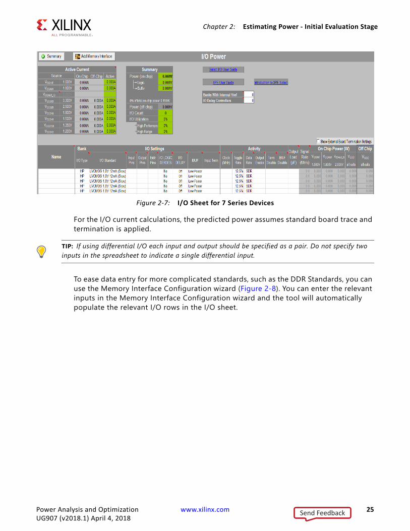
• I/O Power
It is important to fill out the I/O sheet of XPE properly to get an accurate overall estimation of all rails of the chip (see Figure 2-7). Depending on the selected I/O Standard and I/O circuitry, a significant amount of power may be consumed not only in the VCCO rail but also in the VCCINT and VCCAUX rails. Many times it is simplest to enter each device interface separately and also to break out the interface signals to the data, control, and clock signals. This makes it easier to specify different I/O Standards as well as other I/O characteristics such as load and toggle rates.
RECOMMENDED: In XPE, use the Memory Interface Configuration wizard to ease the effort of adding I/Os associated with complex memory interfaces.
X-Ref Target - Figure 2-6
Figure 2-6: Logic Sheet for 7 Series Devices
Power Analysis and Optimization www.xilinx.com 24UG907 (v2018.1) April 4, 2018
Send Feedback
Chapter 2: Estimating Power - Initial Evaluation Stage
For the I/O current calculations, the predicted power assumes standard board trace and termination is applied.
TIP: If using differential I/O each input and output should be specified as a pair. Do not specify two inputs in the spreadsheet to indicate a single differential input.
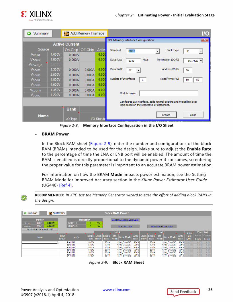
To ease data entry for more complicated standards, such as the DDR Standards, you can use the Memory Interface Configuration wizard (Figure 2-8). You can enter the relevant inputs in the Memory Interface Configuration wizard and the tool will automatically populate the relevant I/O rows in the I/O sheet.
X-Ref Target - Figure 2-7
Figure 2-7: I/O Sheet for 7 Series Devices
Power Analysis and Optimization www.xilinx.com 25UG907 (v2018.1) April 4, 2018
Send Feedback
Chapter 2: Estimating Power - Initial Evaluation Stage
• BRAM Power
In the Block RAM sheet (Figure 2-9), enter the number and configurations of the block RAM (BRAM) intended to be used for the design. Make sure to adjust the Enable Rate to the percentage of time the ENA or ENB port will be enabled. The amount of time the RAM is enabled is directly proportional to the dynamic power it consumes, so entering the proper value for this parameter is important to an accurate BRAM power estimation.
For information on how the BRAM Mode impacts power estimation, see the Setting BRAM Mode for Improved Accuracy section in the Xilinx Power Estimator User Guide (UG440) [Ref 4].
RECOMMENDED: In XPE, use the Memory Generator wizard to ease the effort of adding block RAMs in the design.
X-Ref Target - Figure 2-8
Figure 2-8: Memory Interface Configuration in the I/O Sheet
X-Ref Target - Figure 2-9
Figure 2-9: Block RAM Sheet
Power Analysis and Optimization www.xilinx.com 26UG907 (v2018.1) April 4, 2018
Send Feedback
Chapter 2: Estimating Power - Initial Evaluation Stage
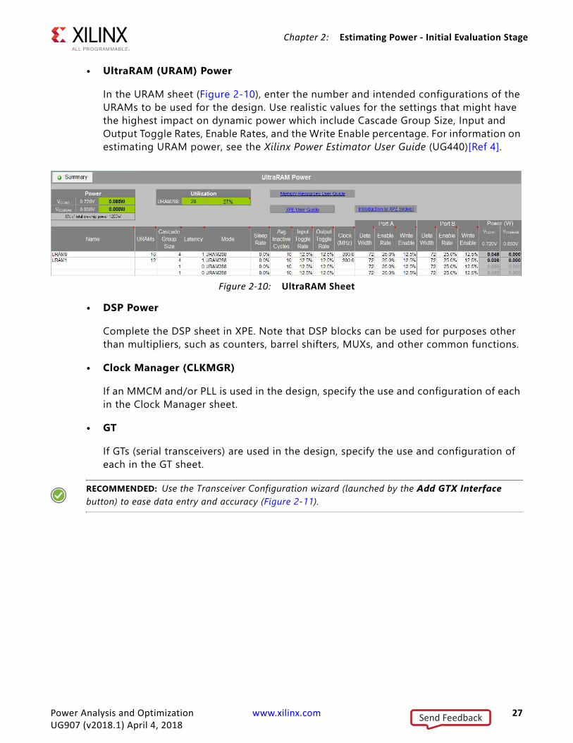
• UltraRAM (URAM) Power
In the URAM sheet (Figure 2-10), enter the number and intended configurations of the URAMs to be used for the design. Use realistic values for the settings that might have the highest impact on dynamic power which include Cascade Group Size, Input and Output Toggle Rates, Enable Rates, and the Write Enable percentage. For information on estimating URAM power, see the Xilinx Power Estimator User Guide (UG440)[Ref 4].
• DSP Power
Complete the DSP sheet in XPE. Note that DSP blocks can be used for purposes other than multipliers, such as counters, barrel shifters, MUXs, and other common functions.
• Clock Manager (CLKMGR)
If an MMCM and/or PLL is used in the design, specify the use and configuration of each in the Clock Manager sheet.
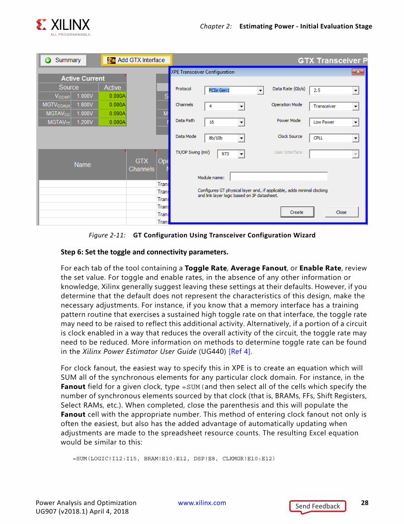
• GT
If GTs (serial transceivers) are used in the design, specify the use and configuration of each in the GT sheet.
RECOMMENDED: Use the Transceiver Configuration wizard (launched by the Add GTX Interface button) to ease data entry and accuracy (Figure 2-11).
X-Ref Target - Figure 2-10
Figure 2-10: UltraRAM Sheet
Power Analysis and Optimization www.xilinx.com 27UG907 (v2018.1) April 4, 2018
Send Feedback
Chapter 2: Estimating Power - Initial Evaluation Stage
Step 6: Set the toggle and connectivity parameters.
For each tab of the tool containing a Toggle Rate, Average Fanout, or Enable Rate, review the set value. For toggle and enable rates, in the absence of any other information or knowledge, Xilinx generally suggest leaving these settings at their defaults. However, if you determine that the default does not represent the characteristics of this design, make the necessary adjustments. For instance, if you know that a memory interface has a training pattern routine that exercises a sustained high toggle rate on that interface, the toggle rate may need to be raised to reflect this additional activity. Alternatively, if a portion of a circuit is clock enabled in a way that reduces the overall activity of the circuit, the toggle rate may need to be reduced. More information on methods to determine toggle rate can be found in the Xilinx Power Estimator User Guide (UG440) [Ref 4].
For clock fanout, the easiest way to specify this in XPE is to create an equation which will SUM all of the synchronous elements for any particular clock domain. For instance, in the Fanout field for a given clock, type =SUM(and then select all of the cells which specify the number of synchronous elements sourced by that clock (that is, BRAMs, FFs, Shift Registers, Select RAMs, etc.). When completed, close the parenthesis and this will populate the Fanout cell with the appropriate number. This method of entering clock fanout not only is often the easiest, but also has the added advantage of automatically updating when adjustments are made to the spreadsheet resource counts. The resulting Excel equation would be similar to this:
=SUM(LOGIC!I12:I15, BRAM!E10:E12, DSP!E8, CLKMGR!E10:E12)
X-Ref Target - Figure 2-11
Figure 2-11: GT Configuration Using Transceiver Configuration Wizard
Power Analysis and Optimization www.xilinx.com 28UG907 (v2018.1) April 4, 2018
Send Feedback

Chapter 2: Estimating Power - Initial Evaluation Stage
For logic fanout, the nature of the data and control paths need to be thought out. In designs with well structured sequential data paths, such as DSP designs, fanouts generally tend to be lower than the set default. In designs with many data execution paths, such as in some embedded designs, higher fanouts may be seen. As with toggle rates, if this information is not known it is best to leave the setting at the default and adjust later if needed.
For I/O Output Load, enter a simple capacitive load for each design output. This will affect the dynamic power of the driven output. The Output Load value is primarily made up from the sum of the individual input capacitances of each device connected to that output. The input capacitance can generally be obtained from the data sheets of the devices to which the FPGA I/O is connected.
Step 7: Analyze the results.
Before you analyze the results, update Steps 1 through 6, if necessary. After completing these steps, analyze the results. Make sure the junction temperature is not exceeded and the power drawn is within the desired budget for the project. If the thermal dissipation or power characteristics are not within targets, adjust the environmental characteristics (that is, more airflow, a heatsink, etc.) or the resource and power characteristics of the design until an acceptable result is reached. Many times, trade-offs can be made to derive the desired functionality with a tighter power budget, and the best time to explore these options is early in the design process. Once the data is completely entered and the part is operating within the thermal limits of the selected grade, the power reported by XPE can be used to specify the rails for the design. If your confidence in the data entered is not very high, you may pad the numbers to circumvent the possibility of underdesigning the power system for the FPGA. If, however, you are fairly certain of the data entered, no additional padding above the data reported by the tool is necessary.
As the design matures, continue to review and update the information in the spreadsheet to reflect the latest requirements and implementation details. This will present the most current picture of the power used in the design and could potentially allow early identification of adjustments to the power budgeting up or down depending on the current power trends of the design.
See Chapter 3, Estimating Power - Vivado Design Flow Stage, which describes a methodology to evaluate your design’s power consumption in the later stage of the design cycle, and Chapter 6, Tips and Techniques for Power Reduction for tips and tricks to reduce power in the design.
Power Analysis and Optimization www.xilinx.com 29UG907 (v2018.1) April 4, 2018
Send Feedback
Chapter 3
Estimating Power - Vivado Design Flow Stage
IntroductionThis chapter describes tool features in the Vivado® Design Suite that automate or simplify power estimation during the design flow stage. Once you generate and analyze a power estimation in the Vivado Design Suite, see Chapter 6, Tips and Techniques for Power Reduction for techniques to investigate and modify your system, to minimize the device power consumption.
Power Estimation ExpectationsAs your design flow progresses through synthesis and implementation you will want to monitor and verify the power consumption regularly. You must ensure that thermal dissipation remains within budget so that you can detect and act early on if any area approaches your constraints. The accuracy of the power estimates varies depending on the design stage when the power was estimated.
Estimating Power in the Vivado IDEThis section covers power analysis using Report Power in the Vivado IDE. These instructions assume this is the first time you are setting up a power analysis after Synthesis. You will therefore provide the tool with the relevant activity information. For subsequent runs, you can choose whether to use Report Power in the Vivado IDE to navigate your Power report or use the Tcl equivalent (report_power) to bypass the Vivado IDE and review the text power report directly.
Power Analysis and Optimization www.xilinx.com 30UG907 (v2018.1) April 4, 2018
Send Feedback

Chapter 3: Estimating Power - Vivado Design Flow Stage
Setting Up Power Analysis from the Vivado IDETo specify the environment, activity, supply, and tool defaults in the Power Analysis window. See Figure 3-1.
1. Select Flow > Open Synthesized Design or Flow > Open Implemented Design.
Alternatively, you can make this selection in the Flow Navigator.
2. Select Reports > Report Power.
Alternatively, you can select Report Power in the Flow Navigator.
3. In the Report Power dialog box, adjust device environment and tool settings.
° Navigating the different tabs in the Report Power dialog box adjusts all settings to closely match your environment.
° Environment and voltage settings have a large influence on device static power.
° Activity rates and voltage settings largely influence dynamic power calculations.
° When unsure of a particular setting, use the default value.
X-Ref Target - Figure 3-1
Figure 3-1: Vivado Power Analysis - Supplying Relevant Input Data for Analysis
Power Analysis and Optimization www.xilinx.com 31UG907 (v2018.1) April 4, 2018
Send Feedback
Chapter 3: Estimating Power - Vivado Design Flow Stage
° If you have an activity file from simulation results, you can specify it in this dialog box.
For more information on these settings, see Review Device/Design Settings and Adjust Activity for Known Elements in Chapter 3.
4. Specify the name of the report.
Running Power Analysis from the Vivado IDEIn the Report Power dialog box, click OK to start the power analysis. The tool does the following:1. Takes into account the environment, device, and tool options.2. Reads the netlist connectivity and configuration.3. Applies activity factors for the nodes you defined.
A node is a component such as a net, pin, or port.
4. Determines activity for any remaining undefined nodes before computing the thermal and supply power.
Power analysis uses different sources of information for activity definition, including:• Simulation files (SAIF)• Automatic calculations using a vectorless power analysis methodology• Manual definition using the set_switching_activity Tcl command.For more information, see Running Power Analysis from the Tcl Prompt.
Vectorless (Probabilistic) EstimationWhen design node activity is not provided either from you or from the simulation results, the vectorless power estimation algorithms are capable of predicting this activity. The vectorless engine assigns initial “seeds” (default signal rates and static probability) to all undefined nodes. Then, starting from the design primary inputs it propagates activity to the output of internal nodes, and repeats this operation until the primary outputs are reached. The algorithm understands the design connectivity and resource functionality and configuration. Its heuristics can even approximate the glitching rate for any nodes in the netlist. Glitching occurs when design elements change states multiple times in between active clock edges before settling to a final value. The vectorless propagation engine is not as accurate as a post-route simulation with a reasonably long duration and realistic stimulus, but it is an excellent compromise between accuracy and compute efficiency.
Power Analysis and Optimization www.xilinx.com 32UG907 (v2018.1) April 4, 2018
Send Feedback
Chapter 3: Estimating Power - Vivado Design Flow Stage
IMPORTANT: The vectorless power estimator does not propagate activity to the output ports of GTs. If any design logic depends on these activity rates, you must explicitly specify the activity rates on GT outputs using set_switching_activity -type <rx_data|tx_data> commands to achieve an accurate analysis.
TIP: The vectorless power estimation is an average power estimation for the design, unless you have specifically overridden switching rates and static probability for the design.
User Input to Improve Vectorless Estimation
In any design, users typically know the activity of specific nodes since they are imposed by the system specification or the interfaces with which the FPGA communicates. Providing this information to the tools, especially for nodes which drive multiple cells in the FPGA (Set, Reset, Clock Enable, or clock signals), will help guide the power estimation algorithms.
These nodes include:
• Clock Activity
Users typically know the exact frequency of all FPGA clock domains, whether externally provided (input ports), internally generated, or externally supplied to the printed circuit board (output ports).
The design should have at least one clock specified using the create_clock constraint. If no clock is defined, then Report Power issues a warning message and uses a 10GHz clock frequency for switching activity computations.
• I/O Data Ports
With your knowledge of the exact protocols and format of the data flowing in and out of the FPGA, you can usually specify signal transition rate and/or signal static probability rate in the tools for at least some of the I/Os. For example, some protocols have a DC balanced requirement (signal static probability rate =50%) or you may know how often data is written or read from your memory interface, so you can set the data rate of strobe and data signals.
If no user activity rate is specified on primary inputs, Report Power will assign a default static probability of 0.5 and a default toggle rate of 12.5%.
• I/O and Internal Control Signals
With your knowledge of the system and the expected functionality you may be able to predict the activity on control signals such as Set, Reset and Clock Enable. These signals typically can turn on or off large pieces of the design logic, so providing this activity information will increase the power estimation accuracy.
Power Analysis and Optimization www.xilinx.com 33UG907 (v2018.1) April 4, 2018
Send Feedback
Chapter 3: Estimating Power - Vivado Design Flow Stage
If a primary input is found to be reset (that is, directly connected to the RESET pin of sequential elements), then the tool will assign a default static probability of 0 and a default signal rate of 0. Similarly, if a primary input is found to be Clock Enable (that is, directly connected to the CE pin of sequential elements), then the tool will assign a default static probability of 0.99 and a default signal rate of 2.
RECOMMENDED: Providing node activity information to the tools, especially for nodes which drive multiple cells in the FPGA (Set, Reset, Clock Enable, or clock signals), helps guide the power estimation algorithms.
IMPORTANT: The vectorless power estimator does not propagate activity to the output ports of GTs. If any design logic depends on these activity rates, you must explicitly specify the activity rates on GT outputs using set_switching_activity -type gt_txdata|gt_rxdata commands to achieve an accurate analysis.
Vector (SAIF) Based Power EstimationIn parallel with all stages of the design development you will generally perform simulations to verify that the design behaves as expected. Different verification techniques are available depending on the design development state, the design complexity, or company policy. The following paragraphs highlight the valuable data you can capture and common pitfalls related to using this data to perform power analysis. An important factor for getting an accurate power estimation is that the design activity needs to be realistic. It should represent the typical or worst case scenario for data coming into the simulated block. This type of information is not necessarily provided while performing verification or validating functions. Sometimes invalid data is given as input to verify that the system can handle it and remain stable even when invalid data or commands are given to it. Using such test cases to perform power analysis may result in inaccurate power estimation since the design logic is not stimulated as it would be under typical system operation.
• System Transaction Level
Very early in the design cycle, you may have created a description of transactions which occur between devices on a PCB or between the different functions of your FPGA application. You can extract from this the expected activity per functional block for certain I/O ports and most of the clock domains. This information helps you fill in the Xilinx Power Estimator spreadsheet.
• FPGA Description Level
While defining the RTL for your application you may want to verify the functionality by performing behavioral simulations. This helps you verify the data flow and the validity of calculations to the clock cycle. At this stage the exact FPGA resources used, count, and configuration is not available. You can manually extrapolate resource utilization and extract activity for I/O ports or internal control signals (Set, Reset, Clock Enable). This
Power Analysis and Optimization www.xilinx.com 34UG907 (v2018.1) April 4, 2018
Send Feedback
Chapter 3: Estimating Power - Vivado Design Flow Stage
information can be applied to refine the Xilinx Power Estimator spreadsheet information.
Your simulator should be able to extract node activity and export it in the form of a SAIF file. You can save this file for more accurate power analysis in the Vivado design flow, for example after place and route, if you do not plan to run post-implementation simulations.
• FPGA Implementation Level
Simulation can be performed at different stages in the implementation process with different outcomes in terms of the power-related information which can be extracted. This additional information may also be used to refine the Xilinx Power Estimator spreadsheet and the Vivado power analysis as well. It may also save I/O ports and specific module activity, which can later be reused in the Vivado power analysis feature at any stage of design completion: post-synthesis, post-placement, or post-route.
° Post Synthesis: The netlist is mapped to the actual resources available in the target device.
° Post Placement: The netlist components are placed into the actual device resources. With this packing information the final logic resource count and configuration becomes available and you can update the Xilinx Power Estimator spreadsheet for your design.
° Post Routing: After routing is complete all the details about routing resources used and exact timing information for each path in the design are defined. In addition to verifying the implemented circuit functionality under best and worst case gate and routing delays, the simulator can also report the exact activity of internal nodes and include glitching. Power analysis at this level provides you the most accurate power estimation before you actually measure power on your prototype board.
Specifying Switching Activity for the Analysis• Simulation Results (SAIF File)
Vivado Report Power matches nets in the design database with names in the simulation results netlist. The simulation results netlist is a SAIF (Switching Activity Interchange Format) file. For all nets matched, Vivado Report Power will apply switching activity and static probability to calculate the design power. Simulation results may have been generated early in the design flow, before synthesis or placement and routing. In this case it is preferable to capture from the simulation results only module I/O ports activity and let the vectorless engine estimate internal node activity. Functional simulations do not capture glitch activity. Also, Report Power may not be able to match all nodes between the design and the simulation netlist because of logic transformations which happen during implementation (optimizations, replications, gating, retiming, etc.). Nevertheless most primary ports and control signals will be matched and this information provides the tool with realistic activity for the matched nodes. The activity
Power Analysis and Optimization www.xilinx.com 35UG907 (v2018.1) April 4, 2018
Send Feedback
Chapter 3: Estimating Power - Vivado Design Flow Stage
is propagated by the vectorless engine onto the unmatched design portion and increase the accuracy of the power estimation.
Make sure to use the following type of simulation results:
° Ensure test vectors and inputs to the simulation represent the typical or expected behavior of the design. Error handling and corner case simulations do not typically stimulate the logic in the way it would be stimulated under normal operation.
° Post-implementation simulation results are preferred over behavioral simulation results. Full timing simulation would be much more accurate, since it helps with capturing timing glitch information into the SAIF results.
IMPORTANT: Report power uses vectorless algorithm and default switching rates to compute the activity on un-matched design nets with the given SAIF file.This results in different toggle rates in Power Report and it eventually reflects in XPE too. It is recommended not to use VHDL generated .saif files as the timing simulation is supported in Verilog only.
IMPORTANT: In the Vivado IDE, specify a SAIF file name in the Simulation activity file(.saif) field in the Switching tab of the Report Power dialog box to read a SAIF simulation output file and annotate matched netlist elements with the switching activity described in the file. Alternatively use the read_saif Tcl command to read the SAIF simulation output file. Refer to the Vivado Design Suite Tutorial: Power Analysis and Optimization [Ref 5] for the complete use model.
IMPORTANT: To generate a SAIF file from the Vivado simulator for power analysis, refer to the Vivado Design Suite User Guide: Logic Simulation (UG900) [Ref 6].To generate a SAIF file from the Mentor Graphics ModelSim simulator for power analysis within the Vivado® Design Suite, see Xilinx Answer 53544.For full timing simulation, generate a design timing information (SDF) file using the write_sdf command and annotate it while running simulation.
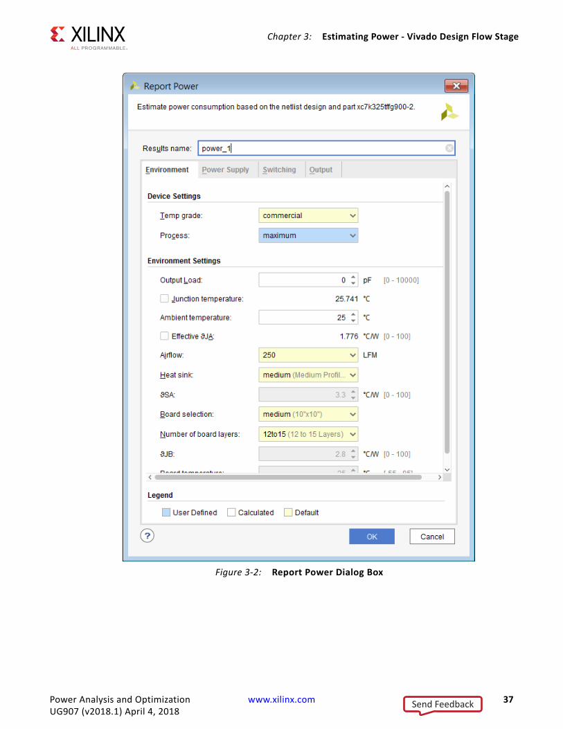
Review Device/Design Settings and Adjust Activity for Known ElementsYou can open the Report Power dialog box from the Flow Navigator window in the Vivado IDE. In this dialog box, you can review power settings and adjust activity for known elements in your design (Figure 3-2).
Power Analysis and Optimization www.xilinx.com 36UG907 (v2018.1) April 4, 2018
Send Feedback
Chapter 3: Estimating Power - Vivado Design Flow Stage
X-Ref Target - Figure 3-2
Figure 3-2: Report Power Dialog Box
Power Analysis and Optimization www.xilinx.com 37UG907 (v2018.1) April 4, 2018
Send Feedback
Chapter 3: Estimating Power - Vivado Design Flow Stage
Review the different input tabs to make sure they accurately represent your expected system. The following Input Tabs are available in Report Power Dialog box:
• Environment Tab• Power Supply Tab• Switching Tab• Output Tab
Environment Tab
Review the different user-editable selections in the Environment tab. Make sure the process, voltage and environment data closely match your expected environment. These settings have a significant influence on the total estimated power.
The user-editable selections in the Environment tab are:
Device Settings
- Temp Grade: Select the appropriate grade for the device (typically Commercial or Industrial). Some devices may have different device static power specifications depending on this setting. Setting this properly will also allow for the proper display of junction temperature limits for the chosen device.
- Process: For the purposes of a worst-case analysis, the recommended process setting is Maximum. The default setting of Typical will give a closer picture to what would be measured statistically, but changing the setting to Maximum will modify the power specification to worst-case values.
Environment Settings
- Output Load (pF): The board and other external capacitance driven by the outputs in the I/O ports.
- Junction Temperature (°C): Specify the maximum possible temperature expected inside the enclosure that will house the FPGA design. This, along with airflow and other thermal dissipation paths (for example, the heatsink), will allow an accurate calculation of Junction Temperature which in turn will allow a more accurate calculation of device static power.
- Airflow (LFM): The airflow across the chip is measured in Linear Feet per Minute (LFM). LFM can be calculated from the fan output in CFM (Cubic Feet per Minute) divided by the cross sectional area through which the air passes. Specific placement of the FPGA and/or fan may have an effect on the effective air movement across the FPGA and thus the thermal dissipation. Note that the default for this parameter is 250 LFM. If you plan to operate the FPGA without active air flow (still air operation) then the 250 LFM default has to be changed to 0 LFM.
Power Analysis and Optimization www.xilinx.com 38UG907 (v2018.1) April 4, 2018
Send Feedback

Chapter 3: Estimating Power - Vivado Design Flow Stage
- Heat Sink (if available): If a heatsink is used and more detailed thermal dissipation information is not available, choose an appropriate profile for the type of heatsink used. This, along with other entered parameters, will be used to help calculate an effective ΘJB, resulting in a more accurate junction temperature and quiescent power calculation. Note that some types of sockets may act as heatsinks, depending on the design and construction of the socket.
- Board Selection and Number of Board Layers (if available): Selecting an approximate size and stack of the board will help calculate the effective ΘJB by taking into account the thermal conductivity of the board itself.
- ΘJB: In the event more accurate thermal modeling of the board and system is available, ΘJB (printed circuit board thermal resistance) should be used in order to specify the amount of heat dissipation expected from the FPGA.
The more accurately custom ΘJB can be specified, the more accurate the estimated junction temperature will be, thus affecting device static power calculations.
IMPORTANT: In order to specify a custom ΘJB, the Board Selection must be set to Custom. If you do specify a custom ΘJB, you must also specify a Board Temperature for an accurate power calculation.
Power Supply Tab:
If this information is known, in the Power Supply tab make sure all voltage levels are set correctly for the different supply sources. Voltage is a large factor contributing to both static and dynamic power.
Switching Tab:
In the Switching tab review the design’s Simulation and Default Activity Settings. The clocks constrained in the design can also be viewed on this page.
Power Analysis and Optimization www.xilinx.com 39UG907 (v2018.1) April 4, 2018
Send Feedback
Chapter 3: Estimating Power - Vivado Design Flow Stage
° Reset switching activity before report power: This check-box if enabled, clears/resets all the switching activity applied before running report power.
° Switching Activity for Resets: Sets the Switching Activity for control sets. See Deassertion of switching for control sets for more information.
° Simulation Settings- Simulation activity file (.saif): Vivado Report Power will take as input SAIF
simulation data generated for the design. Report Power will match nets in the design database with names in the simulation results netlist. See Specifying
X-Ref Target - Figure 3-3
Figure 3-3: Report Power Switching Settings
Power Analysis and Optimization www.xilinx.com 40UG907 (v2018.1) April 4, 2018
Send Feedback

Chapter 3: Estimating Power - Vivado Design Flow Stage
Switching Activity for the Analysis, page 35, for a description of how input from a simulation results (SAIF) file can be used for a more accurate power analysis.
° Default Activity Settings- Default toggle rate: The default toggle rate to be used in power analysis on the
primary inputs of the design. The default toggle rate is set on those primary input nets whose switching activity is not specified by the user, simulation data or constraints of the design. On asynchronous inputs the toggle rate is set with respect to the capturing clock in the design. Valid values are: 0 <= value < 100. The default value is 12.5.
- Default Static Probability: The default static probability to be used in power analysis on the design. The default static probability is set on those primary inputs whose switching activity is not specified by the user, simulation data or constraints of the design. Valid values are: 0 <= value <= 1. The default value is 0.5
° Enable Rate Settings- BRAM Port Enable: Sets the activity rate of all the BRAM enable signals of the
design to the value specified.- BRAM Write Enable: Sets the activity rate of all the BRAM write enable signals
of the design to the value specified.- Bidi Output Port Enable: Sets the activity rate of all the Bidirectional I/O enable
signals (i.e., T pin of IOBUF) of the design to the value specified.Note: Specify Static Probability and the Toggle Rate together.
° Toggle Rate Settings- Primary Outputs: Sets the switching activity rate of all the enable signals (i.e., T
pin of OBUFT) of the primary outputs of the design to the value specified.- Logic:
- Registers: Sets switching activity rate on Output pins of all the Registers in the design.
- Shift Registers: Sets switching activity rate on Output pins of all the Shift Registers in the design.
- Distributed RAMs: Sets switching activity rate on Data Outputs pins of all the Distributed RAMs in the design.
- LUTs: Sets switching activity rate on Outputs pins of all the LUTs in the design.
- DSPs: Sets switching activity rate on Data Outputs pins of all the DSPs in the design.
- Block RAMs: Sets switching activity rate on Data Outputs pins of all the Block RAMs in the design.
Power Analysis and Optimization www.xilinx.com 41UG907 (v2018.1) April 4, 2018
Send Feedback
Chapter 3: Estimating Power - Vivado Design Flow Stage
- GTs (Serial Transceivers):- RX Data: Sets switching activity rate on RX Data Output pins of all the GTs in
the design.- TX Data: Sets switching activity rate on TX Data Output pins of all the GTs in
the design. Note: Specify Static Probability and Toggle Rate together. See the description of the set_switching_activity command under Netlist Element Activity, for more information and guidelines.
• Constrained Clocks: Expanding Constrained Clocks will list all the clocks that are constrained in the design. Review the clock frequencies and ensure they are accurate.
TIP: Make sure all primary clocks are specified. The design clocks are identified based only on create_clock or create_generated_clock constraints.
RECOMMENDED: Xilinx recommends that you use the exact clock frequencies in your design for more accurate power calculation.
Output Tab
Output Tab displays various power result files. Output tab contains the following settings:
° Output Text File:
For project documentation you may want to save the power estimation results. In other circumstances you may be experimenting with different mapping, placement, and routing options to close on performance or area constraints. Saving power results for each experiment will help you select the most power-effective solution when several experiments meet your requirements.
° Output XPE file (for Xilinx Power Estimator)
This file, when selected, saves all the environment information, device usage, and design activity in a file (.xpe) which you can later import into the Xilinx Power Estimator spreadsheet. This proves quite useful when your power budget is exceeded and you don't think that software optimization features alone will be able to meet your budgets. In this case, import the current implementation results into Xilinx Power Estimator, explore different mapping, gating, folding, and other strategies, and estimate their impact on power before modifying the RTL code or rerunning the implementation. You can also compare your assumptions in the Xilinx Power Estimator spreadsheet with these synthesis results and adjust XPE where appropriate.
Power Analysis and Optimization www.xilinx.com 42UG907 (v2018.1) April 4, 2018
Send Feedback
Chapter 3: Estimating Power - Vivado Design Flow Stage
° Output RPX file
This file saves the power report in RPX format, which can later be opened in Vivado GUI by using open_report command.
Run the AnalysisOnce you have provided Report Power with the relevant input data, run the analysis. The tool will start by annotating the netlist with activity from files and user inputs, then apply the tool defaults for the remaining undefined nodes. Next, through an iterative process it will propagate this initial activity from the primary inputs to the primary outputs of your design to refine the activity estimate for the undefined nodes. Finally, it will calculate the dynamic power for each resource used and deduce the additional static power this switching activity generates, to compute the expected junction temperature and total power requirements for the design.
Retaining the Switching Activity Constraints
All the inputs to report_power tool are saved in the XDC constraints of the project and will be populated if report_power tool is invoked again in the flow. This is useful for the what-if analysis. The most recent switching activity constraints are retained and appear in the tool. Even if you provide inputs through XDC based commands in Tcl console of Vivado IDE or through the Net Properties window (Edit Properties in Power tab), these input values will reflect in report_power tool. XDC constraints for switching activity will be in sync with the report_power tool. Any change made in the tool will reflect in the XDC constraints and vice-versa.
This is also helpful, if you want to override the default switching activity in the report_power tool. In this case, you can create XDC constraints with desired default values and run report_power.
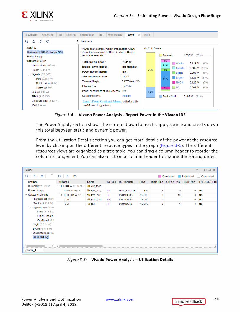
Review Your Design Power DistributionOnce the power analysis is complete you can view the Summary view to review the Total On-Chip Power and thermal properties. The On-Chip Power graph shows the power dissipated in each of the device resource types. With this high-level view you can determine which parts of your design contribute most to the total power (Figure 3-4).
The Summary view also displays a Confidence Level for the power analysis. The Confidence Level is a measurement of the accuracy and the completeness of the input data Report Power uses as it performs a power analysis. If you click the Confidence level value (Low, Medium, or High), Confidence level details are displayed, and these details can suggest ways of increasing the accuracy of the power analysis. For example, you might increase the accuracy of the power analysis by specifying activity rates for more of the clocks or more of the I/O inputs in the design.
Power Analysis and Optimization www.xilinx.com 43UG907 (v2018.1) April 4, 2018
Send Feedback
Chapter 3: Estimating Power - Vivado Design Flow Stage
The Power Supply section shows the current drawn for each supply source and breaks down this total between static and dynamic power.
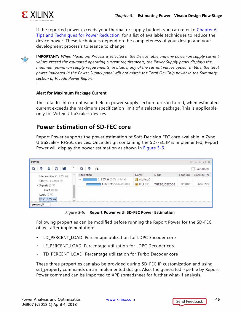
From the Utilization Details section you can get more details of the power at the resource level by clicking on the different resource types in the graph (Figure 3-5). The different resources views are organized as a tree table. You can drag a column header to reorder the column arrangement. You can also click on a column header to change the sorting order.
X-Ref Target - Figure 3-4
Figure 3-4: Vivado Power Analysis - Report Power in the Vivado IDE
X-Ref Target - Figure 3-5
Figure 3-5: Vivado Power Analysis – Utilization Details
Power Analysis and Optimization www.xilinx.com 44UG907 (v2018.1) April 4, 2018
Send Feedback
Chapter 3: Estimating Power - Vivado Design Flow Stage
If the reported power exceeds your thermal or supply budget, you can refer to Chapter 6, Tips and Techniques for Power Reduction, for a list of available techniques to reduce the device power. These techniques depend on the completeness of your design and your development process’s tolerance to change.
IMPORTANT: When Maximum Process is selected in the Device table and any power-on supply current values exceed the estimated operating current requirements, the Power Supply panel displays the minimum power-on supply requirements, in blue. If any of the current values appear in blue, the total power indicated in the Power Supply panel will not match the Total On-Chip power in the Summary section of Vivado Power Report.
Alert for Maximum Package Current
The Total Iccint current value field in power supply section turns in to red, when estimated current exceeds the maximum specification limit of a selected package. This is applicable only for Virtex UltraScale+ devices.
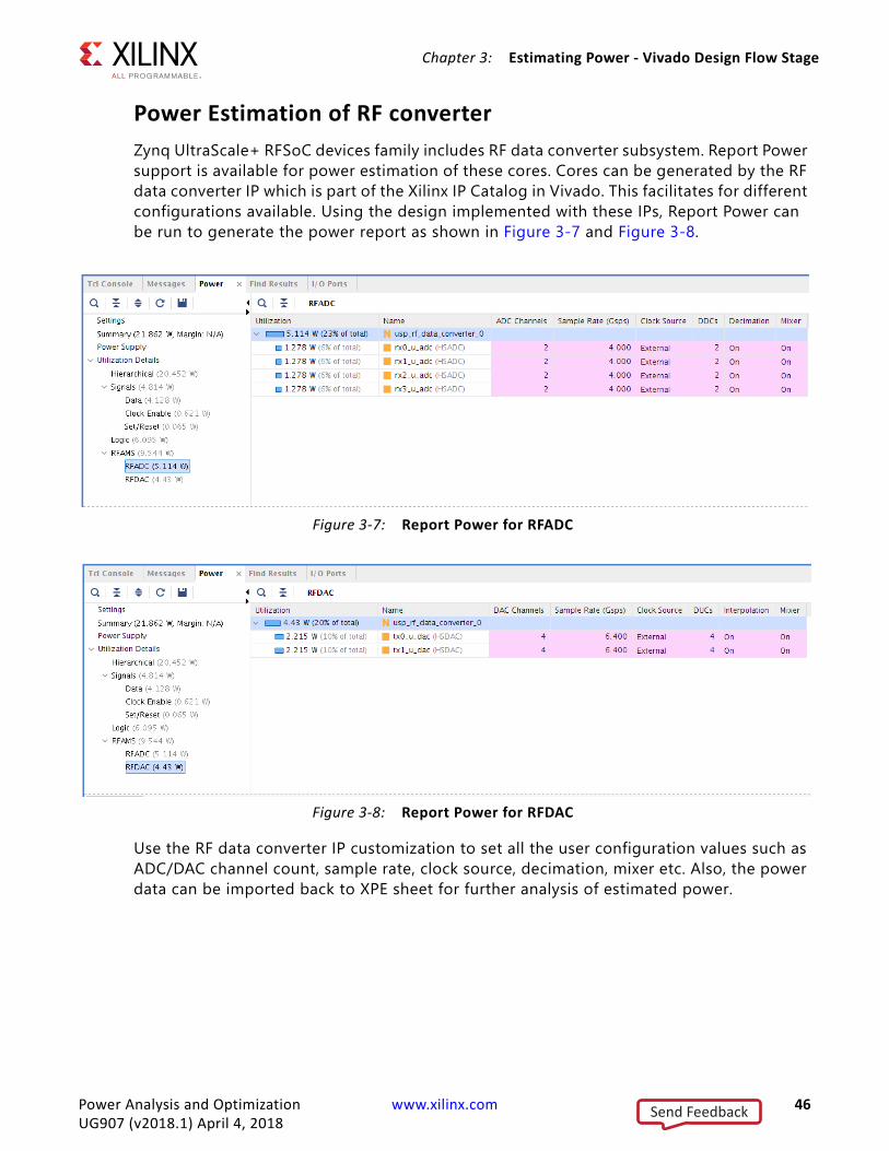
Power Estimation of SD-FEC coreReport Power supports the power estimation of Soft-Decision FEC core available in Zynq UltraScale+ RFSoC devices. Once design containing the SD-FEC IP is implemented, Report Power will display the power estimation as shown in Figure 3-6.
Following properties can be modified before running the Report Power for the SD-FEC object after implementation:
• LD_PERCENT_LOAD: Percentage utilization for LDPC Encoder core• LE_PERCENT_LOAD: Percentage utilization for LDPC Decoder core• TD_PERCENT_LOAD: Percentage utilization for Turbo Decoder core
These three properties can also be provided during SD-FEC IP customization and using set_property commands on an implemented design. Also, the generated .xpe file by Report Power command can be imported to XPE spreadsheet for further what-if analysis.
X-Ref Target - Figure 3-6
Figure 3-6: Report Power with SD-FEC Power Estimation
Power Analysis and Optimization www.xilinx.com 45UG907 (v2018.1) April 4, 2018
Send Feedback
Chapter 3: Estimating Power - Vivado Design Flow Stage
Power Estimation of RF converterZynq UltraScale+ RFSoC devices family includes RF data converter subsystem. Report Power support is available for power estimation of these cores. Cores can be generated by the RF data converter IP which is part of the Xilinx IP Catalog in Vivado. This facilitates for different configurations available. Using the design implemented with these IPs, Report Power can be run to generate the power report as shown in Figure 3-7 and Figure 3-8.
Use the RF data converter IP customization to set all the user configuration values such as ADC/DAC channel count, sample rate, clock source, decimation, mixer etc. Also, the power data can be imported back to XPE sheet for further analysis of estimated power.
X-Ref Target - Figure 3-7
Figure 3-7: Report Power for RFADCX-Ref Target - Figure 3-8
Figure 3-8: Report Power for RFDAC
Power Analysis and Optimization www.xilinx.com 46UG907 (v2018.1) April 4, 2018
Send Feedback
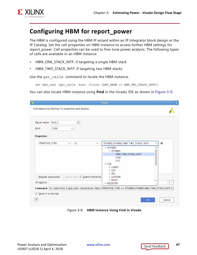
Chapter 3: Estimating Power - Vivado Design Flow Stage
Configuring HBM for report_powerThe HBM is configured using the HBM IP wizard within an IP Integrator block design or the IP Catalog. Set the cell properties on HBM instance to access further HBM settings for report_power. Cell properties can be used to fine-tune power analysis. The following types of cells are available in an HBM instance:
• HBM_ONE_STACK_INTF: if targeting a single HBM stack• HBM_TWO_STACK_INTF: if targeting two HBM stacks
Use the get_cells command to locate the HBM instance.
set hbm_inst [get_cells -hier -filter {REF_NAME == HBM_TWO_STACK_INTF}]
You can also locate HBM instance using Find in the Vivado IDE as shown in Figure 3-9.X-Ref Target - Figure 3-9
Figure 3-9: HBM Instance Using Find in Vivado
Power Analysis and Optimization www.xilinx.com 47UG907 (v2018.1) April 4, 2018
Send Feedback
Chapter 3: Estimating Power - Vivado Design Flow Stage
The property values can be modified before running report_power. The following properties are used for power analysis:
• PAGEHIT_PERCENT_00, PAGEHIT_PERCENT_01: The percentage of cycles that an HBM transaction accesses an open page, which results in the fastest access. For example, sequential memory accesses are more likely to occur within an open page which reduces power and increases efficiency.
• READ_PERCENT_00 to READ_PERCENT_15 (Stack 0), READ_PERCENT_16 to READ_PERCENT_31 (Stack 1): The percentage of cycles that a pseudo-channel is reading from the HBM.
• WRITE_PERCENT_00 to WRITE_PERCENT_15 (Stack 0), WRITE_PERCENT_16 to WRITE_PERCENT_31 (Stack 1): The percentage of cycles that a pseudo-channel is writing to the HBM.
Ensure reasonable values for READ_PERCENT and WRITE_PERCENT based on PAGEHIT_PERCENT. Use the following guidelines:
• PAGEHIT_PERCENT < 75%: READ_PERCENT + WRITE_PERCENT should be 50% or less• PAGEHIT_PERCENT >= 75%: READ_PERCENT + WRITE_PERCENT should be 90% or
lessNote: In the current release, PAGEHIT_PERCENT_00 and PAGEHIT_PERCENT_01 have a default value of 50. The default value will be corrected to 75 in a future release.
The following properties are assigned by HBM IP configuration and are not modified.
• DATARATE_00 to DATARATE_15: Data rate for each memory controller in Gbps. Properties 00 to 07 apply to Stack 0 and 08 to 15 apply to Stack 1.
• SWITCH_ENABLE_00, SWITCH_ENABLE_01: Reflects whether the dedicated AXI switch is enabled or disabled for a stack.
Figure 3-10 is an example of Report Power output for HBM, showing the breakdown of power between the FPGA and HBM stacks.
Power Analysis and Optimization www.xilinx.com 48UG907 (v2018.1) April 4, 2018
Send Feedback
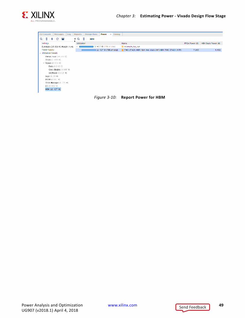
Chapter 3: Estimating Power - Vivado Design Flow Stage
X-Ref Target - Figure 3-10
Figure 3-10: Report Power for HBM
Power Analysis and Optimization www.xilinx.com 49UG907 (v2018.1) April 4, 2018
Send Feedback

Chapter 4
Power Analysis and Optimization in the Vivado Design Suite
IntroductionThis chapter discusses the power-related features and flows available in the Vivado® Design Suite to get you quickly started with power estimation, analysis, and optimization.
You can perform power analysis after synthesis, optimization, placement or routing. It is not supported after RTL elaboration.
You can perform power optimization only before and after placement.
Using either the Vivado IDE or the Tcl prompt, you can perform power analysis and optimization, and can experiment with “What If?” scenarios in a dynamic manner.
Power Analysis in the Vivado IDEThe Vivado IDE power-related capabilities enable the following estimation and analysis features throughout the implementation of your design:
• Reporting the thermal characteristics that impact the static power of the design, including:
° Thermal statistics, such as junction and ambient temperature values
° Data on board selection, including number of board layers and board temperature
° Data on the selection of airflow and the heat sink profile used by the design• Reporting the FPGA current requirements from the different power supply sources• Allowing detailed power distribution analysis to guide power saving strategies to
reduce dynamic, thermal or off-chip power
Figure 4-1 shows the typical power estimation and analysis flow. This includes the main steps required to ensure appropriate tool input and settings before running the estimation
Power Analysis and Optimization www.xilinx.com 50UG907 (v2018.1) April 4, 2018
Send Feedback

Chapter 4: Power Analysis and Optimization in the Vivado Design Suite
or analysis, which ensures the most accurate results. You can run power estimation and analysis commands from the Vivado IDE or the Tcl prompt.
Supported Device Architectures• Vivado Design Suite architecture support is described in the Vivado Design Suite User
Guide: Release Notes, Installation, and Licensing (UG973) [Ref 1].
Supported Inputs• XDC constraints file to specify timing constraints.• Simulation output activity file results from behavioral or timing simulation results (SAIF
files).• XDC/Tcl file commands to specify environment, operating conditions, tool defaults, and
individual netlist nodes activity. For UltraScale+ devices, XPE dumps the XDC files that are sourced from Vivado IDE.
• The Vivado power analysis tool has multiple mechanisms to enter default values and node activity rates. The list below presents the different mechanisms; the list is sorted from highest priority to lowest.1. Static (constant tied to GND or VCC).2. User entered value in any of the Utilization Details views in the Power Results
window.3. Imported simulation activity file (SAIF).
X-Ref Target - Figure 4-1
Figure 4-1: Power Estimation and Analysis Flow
- Generate Netlist: Synthesis or Implementation
X12401
Netlist
- Open Design Netlist- Specify Design Constraint: Timing, Simulation, Block Config- Specify Environment Settings: Device Operating Conditions
Setup
- Run Power Analysis Algorithms- Generate Thermal and Supply Power Distribution Report(s)Run
- Review Power Report- Analyze / Adjust / Experiment with: - Design Activity - Settings: Environment, Device - Tools: Implementation, Analysis
Analyze
Power Analysis and Optimization www.xilinx.com 51UG907 (v2018.1) April 4, 2018
Send Feedback
Chapter 4: Power Analysis and Optimization in the Vivado Design Suite
4. Imported constraint files – Clock constraints imported from constraint files (XDC) or the design netlist.
5. Vectorless estimation – For any node not defined in any of the previously listed inputs, the vectorless estimation will try to estimate activity based on default values combined with the activity of inputs to the node.
6. A default value – For nodes that cannot be estimated by the vectorless estimation a default is assigned, as in the case of design primary inputs and black box outputs.Note: You can adjust default values in the Report Power dialog box. See Review Device/Design Settings and Adjust Activity for Known Elements in Chapter 3 for more information.
Supported Outputs• GUI I/O Bus, Net, and Cell Power properties• GUI and text power reports• XML based power report that can be imported into the Xilinx Power Estimator
spreadsheet tool• Reporting activity rates and operating conditions through Tcl commands.
Further Refining Control Signal ActivityWhen SAIF-based annotation has not been used for accurate power analysis, you can fine-tune the power analysis after doing the first level analysis.
Report Power extracts and lists all the different control signals in the Signal view. You may know from the expected behavior of your application that some Set/Reset signals are not active in normal design operation. In that case, you may want to adjust the activity for these signals. Similarly, some signals in your application may disable entire blocks of the design when the blocks are not in use. Adjust their activity according to the expected functionality.
Because synthesis tool and place and route algorithms can infer or remap control signals to optimize your RTL description, many of the signals listed in these views may be unfamiliar. If you unsure of what these signals are, let the tool determine the activity.
Analyzing Power Reports from the Vivado IDEPower report and analysis windows are integrated into the Vivado IDE workspace (Figure 4-2). These windows enable navigation across the different power views and cross probing to the existing view.
Power Analysis and Optimization www.xilinx.com 52UG907 (v2018.1) April 4, 2018
Send Feedback
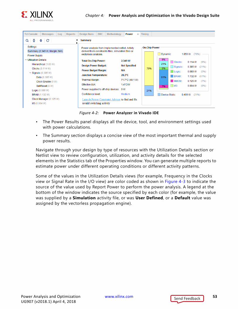
Chapter 4: Power Analysis and Optimization in the Vivado Design Suite
• The Power Results panel displays all the device, tool, and environment settings used with power calculations.
• The Summary section displays a concise view of the most important thermal and supply power results.
Navigate through your design by type of resources with the Utilization Details section or Netlist view to review configuration, utilization, and activity details for the selected elements in the Statistics tab of the Properties window. You can generate multiple reports to estimate power under different operating conditions or different activity patterns.
Some of the values in the Utilization Details views (for example, Frequency in the Clocks view or Signal Rate in the I/O view) are color coded as shown in Figure 4-3 to indicate the source of the value used by Report Power to perform the power analysis. A legend at the bottom of the window indicates the source specified by each color (for example, the value was supplied by a Simulation activity file, or was User Defined, or a Default value was assigned by the vectorless propagation engine).
X-Ref Target - Figure 4-2
Figure 4-2: Power Analyzer in Vivado IDE
Power Analysis and Optimization www.xilinx.com 53UG907 (v2018.1) April 4, 2018
Send Feedback
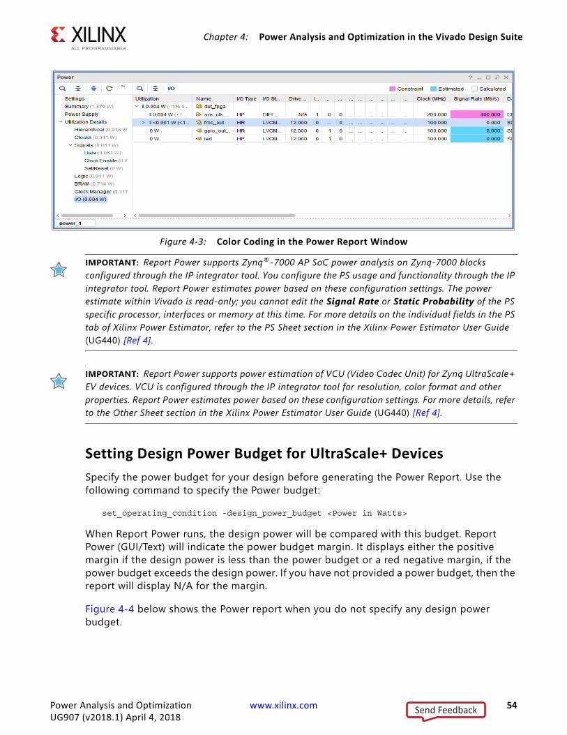
Chapter 4: Power Analysis and Optimization in the Vivado Design Suite
IMPORTANT: Report Power supports Zynq®-7000 AP SoC power analysis on Zynq-7000 blocks configured through the IP integrator tool. You configure the PS usage and functionality through the IP integrator tool. Report Power estimates power based on these configuration settings. The power estimate within Vivado is read-only; you cannot edit the Signal Rate or Static Probability of the PS specific processor, interfaces or memory at this time. For more details on the individual fields in the PS tab of Xilinx Power Estimator, refer to the PS Sheet section in the Xilinx Power Estimator User Guide (UG440) [Ref 4].
IMPORTANT: Report Power supports power estimation of VCU (Video Codec Unit) for Zynq UltraScale+ EV devices. VCU is configured through the IP integrator tool for resolution, color format and other properties. Report Power estimates power based on these configuration settings. For more details, refer to the Other Sheet section in the Xilinx Power Estimator User Guide (UG440) [Ref 4].
Setting Design Power Budget for UltraScale+ DevicesSpecify the power budget for your design before generating the Power Report. Use the following command to specify the Power budget:
set_operating_condition -design_power_budget <Power in Watts>
When Report Power runs, the design power will be compared with this budget. Report Power (GUI/Text) will indicate the power budget margin. It displays either the positive margin if the design power is less than the power budget or a red negative margin, if the power budget exceeds the design power. If you have not provided a power budget, then the report will display N/A for the margin.
Figure 4-4 below shows the Power report when you do not specify any design power budget.
X-Ref Target - Figure 4-3
Figure 4-3: Color Coding in the Power Report Window
Power Analysis and Optimization www.xilinx.com 54UG907 (v2018.1) April 4, 2018
Send Feedback
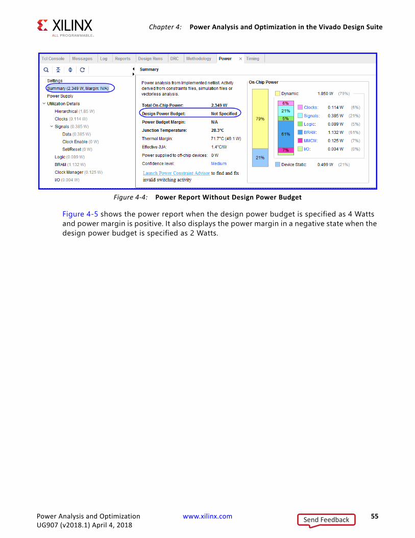
Chapter 4: Power Analysis and Optimization in the Vivado Design Suite
Figure 4-5 shows the power report when the design power budget is specified as 4 Watts and power margin is positive. It also displays the power margin in a negative state when the design power budget is specified as 2 Watts.
X-Ref Target - Figure 4-4
Figure 4-4: Power Report Without Design Power Budget
Power Analysis and Optimization www.xilinx.com 55UG907 (v2018.1) April 4, 2018
Send Feedback
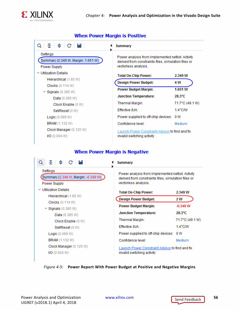
Chapter 4: Power Analysis and Optimization in the Vivado Design Suite
aX-Ref Target - Figure 4-5
Figure 4-5: Power Report With Power Budget at Positive and Negative Margins
Power Analysis and Optimization www.xilinx.com 56UG907 (v2018.1) April 4, 2018
Send Feedback
Chapter 4: Power Analysis and Optimization in the Vivado Design Suite
Save and Restore Power ReportsSave and restore power reports is a new feature introduced in Vivado from 2016.1 release. This feature allows you to save the power reports from Vivado IDE and then reopen them when required. The report will be saved in the rpx format and can be opened at any time using the following Vivado TCL command:
open_report
When you run and open implemented design in the project mode, you will see that the power report impl_1 opens up by default like a timing report.
In the checkpoint flow, you can save the report using -rpx option with report_power tcl command:
report_power -rpx design_1_power.rpx
This saved report can be restored in Vivado IDE using the following tcl command:
open_report -name rpx1 ./design_1_power.rpx
Performing “What If?” Analysis in the Vivado IDETo perform “What If?” analysis, you can set toggle rates and static probability on nets and cells in the design. To make these settings, select any net or cell from the netlist view, schematic, or Power Report, and go to the Power view in the Properties window (Figure 4-6). Then click the Load Properties button in the Power view. Click Edit Properties and set the Toggle Rate and Static Probability in the Edit Power Properties dialog box that appears, and click OK.
Power Analysis and Optimization www.xilinx.com 57UG907 (v2018.1) April 4, 2018
Send Feedback
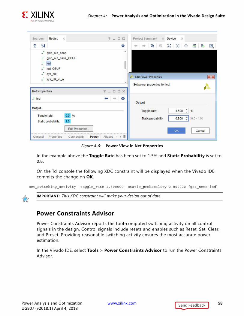
Chapter 4: Power Analysis and Optimization in the Vivado Design Suite
In the example above the Toggle Rate has been set to 1.5% and Static Probability is set to 0.8.
On the Tcl console the following XDC constraint will be displayed when the Vivado IDE commits the change on OK.
set_switching_activity -toggle_rate 1.500000 -static_probability 0.800000 [get_nets led]
IMPORTANT: This XDC constraint will make your design out of date.
Power Constraints AdvisorPower Constraints Advisor reports the tool-computed switching activity on all control signals in the design. Control signals include resets and enables such as Reset, Set, Clear, and Preset. Providing reasonable switching activity ensures the most accurate power estimation.
In the Vivado IDE, select Tools > Power Constraints Advisor to run the Power Constraints Advisor.
X-Ref Target - Figure 4-6
Figure 4-6: Power View in Net Properties
Power Analysis and Optimization www.xilinx.com 58UG907 (v2018.1) April 4, 2018
Send Feedback
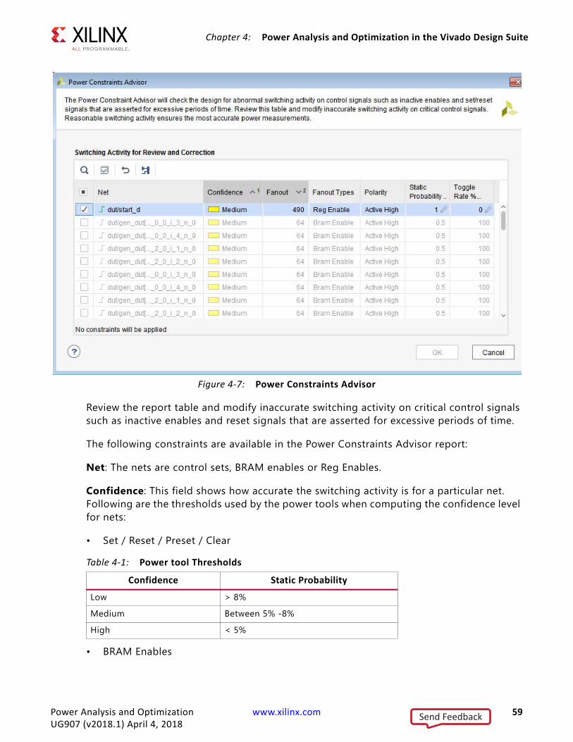
Chapter 4: Power Analysis and Optimization in the Vivado Design Suite
Review the report table and modify inaccurate switching activity on critical control signals such as inactive enables and reset signals that are asserted for excessive periods of time.
The following constraints are available in the Power Constraints Advisor report:
Net: The nets are control sets, BRAM enables or Reg Enables.
Confidence: This field shows how accurate the switching activity is for a particular net. Following are the thresholds used by the power tools when computing the confidence level for nets:
• Set / Reset / Preset / Clear
• BRAM Enables
X-Ref Target - Figure 4-7
Figure 4-7: Power Constraints Advisor
Table 4-1: Power tool ThresholdsConfidence Static Probability
Low > 8%Medium Between 5% -8%High < 5%
Power Analysis and Optimization www.xilinx.com 59UG907 (v2018.1) April 4, 2018
Send Feedback
Chapter 4: Power Analysis and Optimization in the Vivado Design Suite
Low confidence means that the BRAM is not active in the design and should be revisited to check the possibility of removing it.
• Reg Enables
Low Confidence informs you that the Register in the design is not active and should be revisited.
Medium Confidence informs you that the registers are enabled with reasonable amount of time either defined by you or propagated by tool.
Fanout: This field shows the fanout for each control signal, which is the number of driven leaf-level primitives. Signals with higher fanout are the most important for review and correction because they are capable of disabling downstream switching of large portions of the design. This may result in severe under-reporting of power. Low-fanout signals with inaccurate switching will have less impact and are therefore not important.
Fanout Type: This field specifies if the nets are control sets (set, reset, clear, preset) or bram enable. If there are multiple entries for any control net, it means that those particular nets have multiple fanouts and they are driving different pins in fanout cells.
Polarity: This field identifies the polarity for the control set. You should pay attention to the polarity while setting the static probability of a net.
Static probability: This is editable filed and you need to enter the correct activity based on the fanout type and polarity of the net.
Toggle Rate: Toggle rate for the net. This is also editable and you need to enter this field based on the static probability.
Note: By default, PCA will be sorted by Confidence as Low and Fanout as high to low. Also, the column filtering is enabled for PCA wizard. To use column filtering, right-click on header row and click Enable Column Filtering.
The following process is recommended for using the Power Constraints Advisor:
1. Click the Confidence column to sort it so that LOW signals are in top.
Table 4-2: BRAM EnableConfidence Static Probability
Low < 1%
Table 4-3: Reg EnableConfidence Static Probability
Low < 3%Medium > 3%
Power Analysis and Optimization www.xilinx.com 60UG907 (v2018.1) April 4, 2018
Send Feedback
Chapter 4: Power Analysis and Optimization in the Vivado Design Suite
2. Hold down the Ctrl key and click on Fanout column twice to sort it by descending values.
3. Review and define new Static Probability and Toggle Rate for all the control nets which are LOW in confidence with fanout greater than 200.
4. Click OK to apply the constraints to the design and rerun the Report Power command.
The following are some of the examples which will help you to set accurate switching activity for the control sets and BRAM enables:
Active high reset with Static Probability 0.9
This indicates that the reset is high (active) 90% of the time. This means that the load cells are reset for 90% of the time, which is excessive. Change the switching activity to indicate that the reset is inactive, a more realistic condition, by setting the Static Probability to 0 and Toggle Rate to 0.
BRAM Enable with Static Probability 0 and Toggle Rate of 0
This indicates that the BRAM is never enabled, which is overly pessimistic. Assign a more reasonable switching activity on the BRAM Enable such as a 25% enable rate, setting the Static Probability to 0.25 and Toggle Rate to 50. Use the following command to generate the text report for power advisory:
report_power -advisory -file power_report.pwr
Advisory table will be added at the end of the this report file.
Deassertion of switching for control setsYou can deassert all the control sets in the design. This option allows you to match the power number from tools much closely with the hardware number. You will have the option to enable/disable this option from the report power tool or in Tcl mode.
There are three options for setting the switching activity for resets:
• None: This is the default mode. In this mode, the report power tool will not set any value and leave the activities as comes after vector-less propagation.
• Deassert: When you select this option, the report power tool will deassert all the control sets in the design.
• Do Not Deassert: In this mode, changes of deassert option will be reverted back to original value.
Power Analysis and Optimization www.xilinx.com 61UG907 (v2018.1) April 4, 2018
Send Feedback
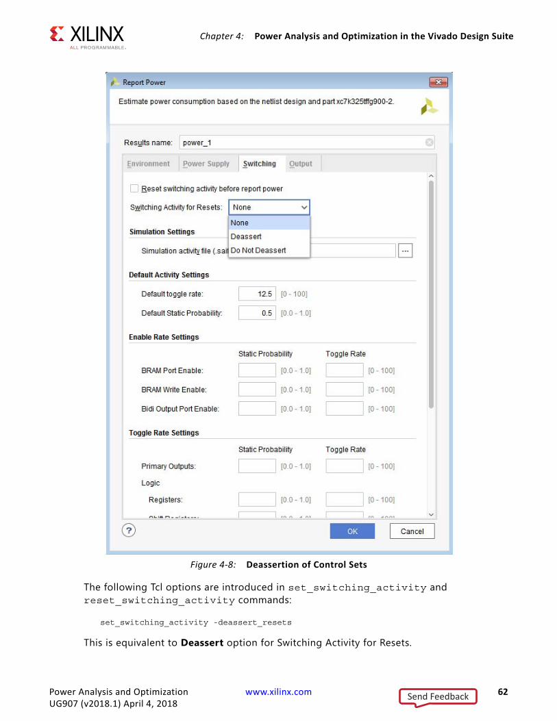
Chapter 4: Power Analysis and Optimization in the Vivado Design Suite
The following Tcl options are introduced in set_switching_activity and reset_switching_activity commands:
set_switching_activity -deassert_resets
This is equivalent to Deassert option for Switching Activity for Resets.
X-Ref Target - Figure 4-8
Figure 4-8: Deassertion of Control Sets
Power Analysis and Optimization www.xilinx.com 62UG907 (v2018.1) April 4, 2018
Send Feedback
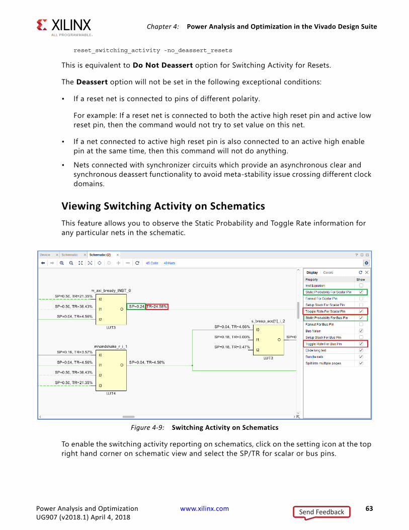
Chapter 4: Power Analysis and Optimization in the Vivado Design Suite
reset_switching_activity -no_deassert_resets
This is equivalent to Do Not Deassert option for Switching Activity for Resets.
The Deassert option will not be set in the following exceptional conditions:
• If a reset net is connected to pins of different polarity.
For example: If a reset net is connected to both the active high reset pin and active low reset pin, then the command would not try to set value on this net.
• If a net connected to active high reset pin is also connected to an active high enable pin at the same time, then this command will not do anything.
• Nets connected with synchronizer circuits which provide an asynchronous clear and synchronous deassert functionality to avoid meta-stability issue crossing different clock domains.
Viewing Switching Activity on SchematicsThis feature allows you to observe the Static Probability and Toggle Rate information for any particular nets in the schematic.
To enable the switching activity reporting on schematics, click on the setting icon at the top right hand corner on schematic view and select the SP/TR for scalar or bus pins.
X-Ref Target - Figure 4-9
Figure 4-9: Switching Activity on Schematics
Power Analysis and Optimization www.xilinx.com 63UG907 (v2018.1) April 4, 2018
Send Feedback
Chapter 4: Power Analysis and Optimization in the Vivado Design Suite
Power Analysis Using the Tcl InterfaceThis section describes each step in a typical power analysis flow using the Tcl interface. The following section, Power Analysis Tcl Commands, lists the commands related to power analysis.
For information on options, properties, applicable elements, or returned values for a specific command:
• Type <command_name> -help, or • See the Vivado Design Suite Tcl Command Reference Guide (UG835) [Ref 2].• See the Vivado Design Suite User Guide: Using Constraints (UG903) [Ref 3].
Power Analysis Tcl Commands
• read_saif
• set_switching_activity
• set_operating_conditions
• report_switching_activity
• report_operating_conditions
• report_power
• reset_switching_activity
• reset_operating_conditions
• set_units
Timing Constraints that Influence Power Analysis
• create_clock
• create_generated_clock
• set_input_delay
• set_case_analysis
Power Analysis and Optimization www.xilinx.com 64UG907 (v2018.1) April 4, 2018
Send Feedback
Chapter 4: Power Analysis and Optimization in the Vivado Design Suite
Setting Up Power Analysis from the Tcl PromptBefore running power estimations, you must provide the tool with information about the device environment and the known switching activity rates for the design netlist. This ensures the accuracy of the power estimation.
• Device Environment• Netlist Element Activity• set_case_analysis
Device Environment
Specify all device operating conditions settings such as:
• Thermal, for example:
° Ambient temperature
° Heat sink• Voltage, for example:
° VCCINT
° VCCAUX
° VCCO• Device, for example:
° Temperature grade
° Process corner
Use the following commands:
• report_operating_conditions
Report all or the specified operating condition settings. Examples are:report_operating_conditions # Reports all
report_operating_conditions -voltage
• set_operating_conditions
Modify the specified operating condition parameters. Examples are:set_operating_conditions -process maximum -junction_temperature 50
set_operating_conditions -voltage {vccint 0.97 vccaux 1.71}
• reset_operating_conditions
Return all or the specified operating condition parameters to the default values for the selected device. Examples are:
Power Analysis and Optimization www.xilinx.com 65UG907 (v2018.1) April 4, 2018
Send Feedback
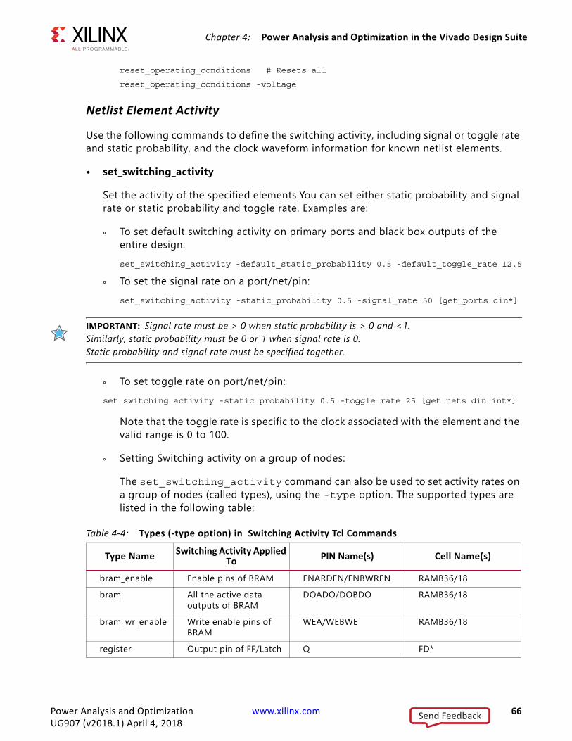
Chapter 4: Power Analysis and Optimization in the Vivado Design Suite
reset_operating_conditions # Resets all
reset_operating_conditions -voltage
Netlist Element Activity
Use the following commands to define the switching activity, including signal or toggle rate and static probability, and the clock waveform information for known netlist elements.
• set_switching_activity
Set the activity of the specified elements.You can set either static probability and signal rate or static probability and toggle rate. Examples are:
° To set default switching activity on primary ports and black box outputs of the entire design:set_switching_activity -default_static_probability 0.5 -default_toggle_rate 12.5
° To set the signal rate on a port/net/pin:set_switching_activity -static_probability 0.5 -signal_rate 50 [get_ports din*]
IMPORTANT: Signal rate must be > 0 when static probability is > 0 and <1. Similarly, static probability must be 0 or 1 when signal rate is 0.Static probability and signal rate must be specified together.
° To set toggle rate on port/net/pin:set_switching_activity -static_probability 0.5 -toggle_rate 25 [get_nets din_int*]
Note that the toggle rate is specific to the clock associated with the element and the valid range is 0 to 100.
° Setting Switching activity on a group of nodes:
The set_switching_activity command can also be used to set activity rates on a group of nodes (called types), using the -type option. The supported types are listed in the following table:
Table 4-4: Types (-type option) in Switching Activity Tcl Commands
Type Name Switching Activity Applied To PIN Name(s) Cell Name(s)
bram_enable Enable pins of BRAM ENARDEN/ENBWREN RAMB36/18bram All the active data
outputs of BRAMDOADO/DOBDO RAMB36/18
bram_wr_enable Write enable pins of BRAM
WEA/WEBWE RAMB36/18
register Output pin of FF/Latch Q FD*
Power Analysis and Optimization www.xilinx.com 66UG907 (v2018.1) April 4, 2018
Send Feedback
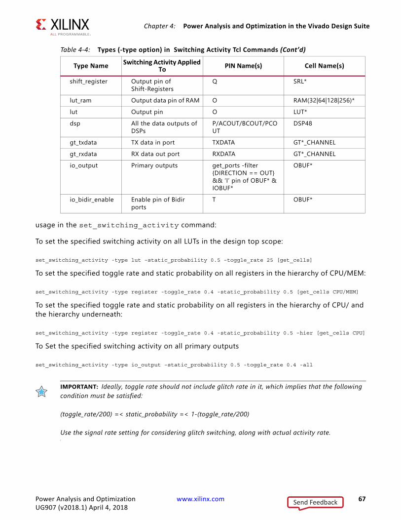
Chapter 4: Power Analysis and Optimization in the Vivado Design Suite
usage in the set_switching_activity command:
To set the specified switching activity on all LUTs in the design top scope:
set_switching_activity -type lut –static_probability 0.5 –toggle_rate 25 [get_cells]
To set the specified toggle rate and static probability on all registers in the hierarchy of CPU/MEM:
set_switching_activity -type register -toggle_rate 0.4 -static_probability 0.5 [get_cells CPU/MEM]
To set the specified toggle rate and static probability on all registers in the hierarchy of CPU/ and the hierarchy underneath:
set_switching_activity -type register -toggle_rate 0.4 -static_probability 0.5 –hier [get_cells CPU]
To Set the specified switching activity on all primary outputs
set_switching_activity -type io_output –static_probability 0.5 -toggle_rate 0.4 -all
IMPORTANT: Ideally, toggle rate should not include glitch rate in it, which implies that the following condition must be satisfied:
(toggle_rate/200) =< static_probability =< 1-(toggle_rate/200)
Use the signal rate setting for considering glitch switching, along with actual activity rate.
shift_register Output pin of Shift-Registers
Q SRL*
lut_ram Output data pin of RAM O RAM(32|64|128|256)*lut Output pin O LUT*dsp All the data outputs of
DSPsP/ACOUT/BCOUT/PCOUT
DSP48
gt_txdata TX data in port TXDATA GT*_CHANNELgt_rxdata RX data out port RXDATA GT*_CHANNELio_output Primary outputs get_ports -filter
{DIRECTION == OUT} && ‘I’ pin of OBUF* & IOBUF*
OBUF*
io_bidir_enable Enable pin of Bidir ports
T OBUF*
Table 4-4: Types (-type option) in Switching Activity Tcl Commands (Cont’d)
Type Name Switching Activity Applied To PIN Name(s) Cell Name(s)
Power Analysis and Optimization www.xilinx.com 67UG907 (v2018.1) April 4, 2018
Send Feedback
Chapter 4: Power Analysis and Optimization in the Vivado Design Suite
IMPORTANT: The set_switching_activity command will not have any effect on design clock nets. To change the activity on the clock nets, please use timing constraints (create_clock, create_generated_clock, set_case_analysis etc).
• report_switching_activity
Reports the activity of the specified elements. Displays static probability, signal rate and toggle rate. The command also displays the source of the assigned switching activity.
Examples of report_switching_activity commands are:
° Report static probability, signal rate, and toggle rate for a single net:Vivado% report_switching_activity -static_probability [get_ports clk_p]
clk_p: static probability = 0.5 (C)
Vivado% report_switching_activity [get_ports clk_p]
clk_p: static probability = 0.5 (C) signal rate = 400 (C) toggle rate = 200 (C)
The source of the assigned switching activity is expressed as: (C)=XDC Constraints, (D)=Tool Default, (S)= SAIF Annotated, (A)=User Assigned.
° Report on group nodes:- To report switching activity for all distributed RAMs in the hierarchy CPU/:
report_switching_activity –type lut_ram [get_cells CPU/*]
- To report switching activity for all GT RXDATA in the design:report_switching_activity –type gt_rxdata -all
See Table 4-4 for information on the supported types.
• reset_switching_activity
Resets the activity rates (static probability, signal rate, and toggle rate) on specific netlist elements to the tool default value. The command resets both user specified values and Simulation activity rate settings. Examples are:
° To reset default switching activity on primary ports and black box outputs of the entire design:
reset_switching_activity -default
° To reset activity rates on the entire design:reset_switching_activity -all
° To reset activity rate on specific port/net/pin:reset_switching_activity [get_ports din*]
° To reset activity rates on a group of nodes:
Power Analysis and Optimization www.xilinx.com 68UG907 (v2018.1) April 4, 2018
Send Feedback
Chapter 4: Power Analysis and Optimization in the Vivado Design Suite
- To reset the switching activity for all BRAM enables (ENARDEN/ENBWREN) in the entire design:
reset_switching_activity –type bram_enable -all
- To reset the switching activity for all LUTs in the hierarchy CPU/ and levels underneath:
reset_switching_activity –type lut –hier [get_cells CPU/MEM]
See Table 4-4 for information on the supported types.
• read_saif
Read an SAIF simulation output file and annotate matched netlist elements with the switching activity described in the file. An examples is:
read_saif -out_file read_saif.rpt -strip_path tb/tb_core/core -file routed.saif
Options to read_saif are:
-out_file - Dumps the unmatched simulation and design nets list into a file.
-strip_path - By default it is assumed that the design top is instantiated in the testbench. Thus the first two levels of hierarchy are stripped while annotating SAIF data into the design. If the simulation setup has multiple hierarchy levels, then you are expected to specify the hierarchy to be stripped off from SAIF to better match the actual design.
The read_saif command also displays the SAIF annotation summary to show the number of design nets matched. Ideally 100% design net match is expected for an accurate analysis.
IMPORTANT: If your design contains any encrypted IP/Blocks, your simulator will not dump the SAIF information for those IP/Blocks and for any internal blocks within the encrypted hierarchy. This incomplete SAIF information might affect the power estimation accuracy. The read_saif command will not modify the activities on the design clock nets. Clock nets activities will be driven by the timing constraints.
read_saif command can be executed multiple times with each saif file. This will enable you to read multiple saif files for different blocks in design. Report power then estimates the power by considering the switching activity information from all the saif files. If common nets exist in multiple saif files, then the switching activity will be applied from the last read saif file using read_saif command.
• create_clock
Synthesis and implementation constraint to specify clock waveforms. An example is:
Power Analysis and Optimization www.xilinx.com 69UG907 (v2018.1) April 4, 2018
Send Feedback
Chapter 4: Power Analysis and Optimization in the Vivado Design Suite
create_clock -name clk -period 5 [get_ports clk]; # 200MHz
• create_generated_clock
Synthesis and implementation constraint to specify generated clock waveforms. An example is:
create_generated_clock -name gen_clk -source clk1 -divide_by 2 [get_net -hier sys_clk]
• set_input_delay
Associates primary inputs to the specific clock. This is very important in a multi-clock design, especially if the primary port is launched at a different clock. An example is:
create_clock -name clk1 -period 5 [get_ports clk]
set_input_delay -clock clk1 1 [get_ports d]
Note: If the primary ports are not associated with any clock, then the switching rate is computed based on the capturing clock in the path.
By default, create_clock and create_generated_clock are defined in the XDC file and you need not rerun them. However, to do “What If?” analysis, such as by changing the clock frequency for Report Power, create_clock or create_generated_clock must be used to reflect the change.
• set_case_analysis
For global clock primitives (BUFG, BUFGCE, BUFGCE_DIV, BUFG_GT, BUFGCTRL), the enable / selection of clock is determined by set_case_analysis command. This command guides the timing analyzer to identify the clocks across clocking logic. For example the select signal of BUFGMUX must be set using set_case_analysis to guide the timing analyzer's clock selection. This in turn helps Report Power to estimate power using the right clock. For BUGCE block, CE input must be set using set_case_analysis to enable or disable the clock output.
Minimum Input Set
Before performing power estimation:
• Make sure the activity is defined for all clocks in your netlist.• If possible, specify the activity of all primary input ports in your design using the Tcl
commands or reading a simulation output file. These port activity rates determine the internal logic activity rates. Therefore, if the tool’s default settings do not match your application, the internal logic activity may be overestimated or underestimated.
• If known, specify the activity of any high fanout nets that you defined in your HDL code, such as global set, reset, and clock enable signals.
When reading the simulation result file, make sure the activity is representative of the worst case design functional activity (that is, the simulation result at which the maximum design
Power Analysis and Optimization www.xilinx.com 70UG907 (v2018.1) April 4, 2018
Send Feedback
Chapter 4: Power Analysis and Optimization in the Vivado Design Suite
code coverage is achieved). Using simulation results from basic and corner case tests can lead to inaccurate power estimations.
Running Power Analysis from the Tcl PromptAfter all environment and activity settings are defined, you can run the power analysis algorithm using the report_power command. An example is:
Vivado% report_power -file routed.pwr -xpe design_top.xpe
The tool does the following:
1. Loads your environment settings and design netlist.2. Annotates activity for any netlist element you specified with input files or Tcl
commands. Note: For all undefined nodes, the tool uses the vectorless propagation engine to estimate activity, taking into account activity of known elements and logic configuration and connectivity.
3. Calculates and reports the design thermal and supply power.
Analyzing Power Reports from the Tcl PromptTo analyze the design power, start by reviewing the total thermal and supply power information in the power report (Figure 4-10).
Then, depending on your design margin against requirements, you can review the resource or hierarchy sections. These sections show the design power distribution at a more detailed level. As a result of your analysis, you may want to return to Xilinx Power Estimator and perform design architectural scenarios.
You can also perform "What If?" scenarios to evaluate the impact of changes in the settings for:• Environment• Device• Implementation• Power tool
Power Analysis and Optimization www.xilinx.com 71UG907 (v2018.1) April 4, 2018
Send Feedback
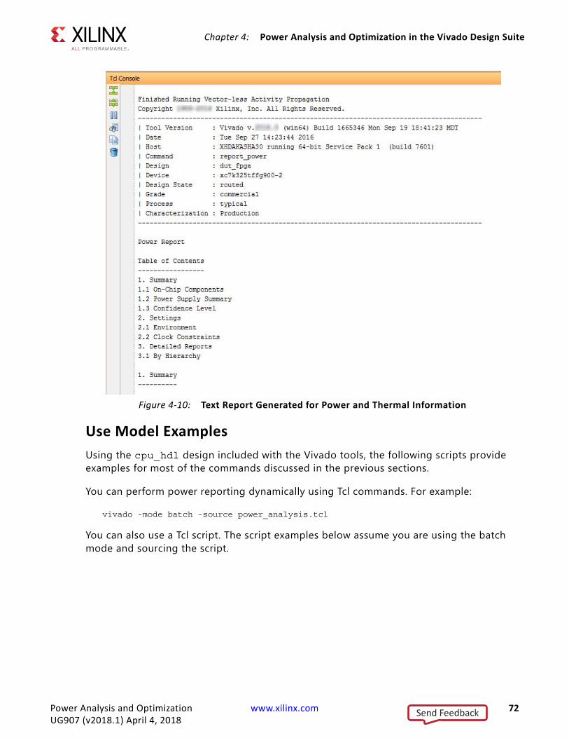
Chapter 4: Power Analysis and Optimization in the Vivado Design Suite
Use Model ExamplesUsing the cpu_hdl design included with the Vivado tools, the following scripts provide examples for most of the commands discussed in the previous sections.
You can perform power reporting dynamically using Tcl commands. For example:
vivado -mode batch -source power_analysis.tcl
You can also use a Tcl script. The script examples below assume you are using the batch mode and sourcing the script.
X-Ref Target - Figure 4-10
Figure 4-10: Text Report Generated for Power and Thermal Information
Power Analysis and Optimization www.xilinx.com 72UG907 (v2018.1) April 4, 2018
Send Feedback
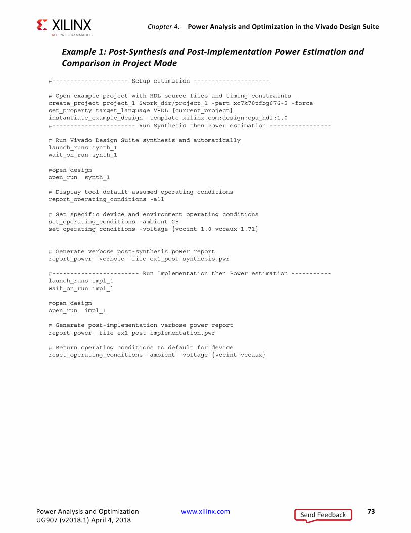
Chapter 4: Power Analysis and Optimization in the Vivado Design Suite
Example 1: Post-Synthesis and Post-Implementation Power Estimation and Comparison in Project Mode
#--------------------- Setup estimation ---------------------
# Open example project with HDL source files and timing constraintscreate_project project_1 $work_dir/project_1 -part xc7k70tfbg676-2 -force set_property target_language VHDL [current_project]instantiate_example_design -template xilinx.com:design:cpu_hdl:1.0#----------------------- Run Synthesis then Power estimation -----------------
# Run Vivado Design Suite synthesis and automaticallylaunch_runs synth_1wait_on_run synth_1
#open designopen_run synth_1
# Display tool default assumed operating conditionsreport_operating_conditions -all
# Set specific device and environment operating conditionsset_operating_conditions -ambient 25set_operating_conditions -voltage {vccint 1.0 vccaux 1.71}
# Generate verbose post-synthesis power reportreport_power -verbose -file ex1_post-synthesis.pwr
#------------------------ Run Implementation then Power estimation -----------launch_runs impl_1wait_on_run impl_1
#open designopen_run impl_1
# Generate post-implementation verbose power reportreport_power -file ex1_post-implementation.pwr
# Return operating conditions to default for devicereset_operating_conditions -ambient -voltage {vccint vccaux}
Power Analysis and Optimization www.xilinx.com 73UG907 (v2018.1) April 4, 2018
Send Feedback

Chapter 4: Power Analysis and Optimization in the Vivado Design Suite
Example 2: Post-Synthesis and Post-Implementation Power Estimation and Comparison in Projectless Mode
#--------------------- Setup estimation ---------------------
# Open netlist in projectless mode read_edif -name top.edf
# AND link the designlink_design
# OR open Vivado checkpoint open_checkpoint -file post_synth.dcp
# read design constraints, if it is not part of a design checkpoint (DCP)read_xdc -name top_full.xdc
# Display tool default assumed operating conditionsreport_operating_conditions -all
# Set specific device and environment operating conditionsset_operating_conditions -ambient 25set_operating_conditions -voltage {vccint 0.95 vccaux 1.71}
#---------------------- Power estimation at post synthesis ----------------
# Generate verbose post-synthesis power reportreport_power -verbose -file ex1_post-synthesis.pwr
#----Run various Implementation steps then run Power estimation after every step ----opt_designreport_power -verbose -file ex1_post-opt_design.pwrpower_opt_design ;# Optional report_power -verbose -file ex1_post_pwr_opt_design.pwrplace_design report_power -verbose -file ex1_post_place_design.pwrphys_opt_design ;# Optionalreport_power -verbose -file ex1_post_phys_opt_design.pwrroute_design
# Generate post-route verbose power reportreport_power -verbose -file ex1_post_route_design.pwr
# Return operating conditions to default for devicereset_operating_conditions -ambient -voltage {vccint vccaux}
Example 3: Examine and ensure Static Probability values on resets are accurate
# Query the Static Probability value of the resetreport_switching_activity -static_probability [get_ports reset]# Output is - reset: static probability = 0.5 (D)
# Set Static Probability value and signal rate of reset to 0set_switching_activity -static_probability 0.0 -toggle_rate 0 [get_ports reset]
# Generate post-route verbose power reportreport_power -verbose -file ex1_post_route_design.pwr
Power Analysis and Optimization www.xilinx.com 74UG907 (v2018.1) April 4, 2018
Send Feedback
Chapter 4: Power Analysis and Optimization in the Vivado Design Suite
Example 4: What If? Design Analysis/Report, Edit, and Reset Design Activity
Working with power analysis can be very dynamic, allowing you to explore “What If?” scenarios on the fly. Open the previously implemented design, and enter or source the following commands. This modifies activity for control signals (clock enable and reset) in submodule fftEngine to evaluate the impact on power for this hierarchical level and the entire design.
#---------------- Report power and activity with default settings ------------
# Report power report_power -file ex3_power_before.pwr
# Get activity of signals of interestreport_switching_activity [get_nets {fftEngine/reset fftEngine/wb_we_i_reg}]
#---------- scenario with no reset and higher CE activity --------------
# disable reset and enable clock enables in module fftEngine most of the timeset_switching_activity -static_probability 0 -signal_rate 0 [get_nets fftEngine/reset_reg]set_switching_activity -static_probability 1 -toggle_rate 0 [get_nets fftEngine/wb_we_i_reg]report_power -file ex3_power_no_reset_activ.pwrreport_switching_activity [get_nets fftEngine/reset_reg fftEngine/wb_we_i_reg]
#----------- scenario with active reset and low CE activity ---------
# enable reset and disable clock enable in module fftEngine most of the timeset_switching_activity -static_probability 1 -toggle_rate 0 [get_nets fftEngine/reset_reg]set_switching_activity -static_probability 0 -signal_rate 0 [get_nets fftEngine/wb_we_i_reg]report_power -file ex3_power_reset_activ.pwrreport_switching_activity [get_nets fftEngine/reset_reg fftEngine/wb_we_i_reg]
Power Analysis and Optimization www.xilinx.com 75UG907 (v2018.1) April 4, 2018
Send Feedback
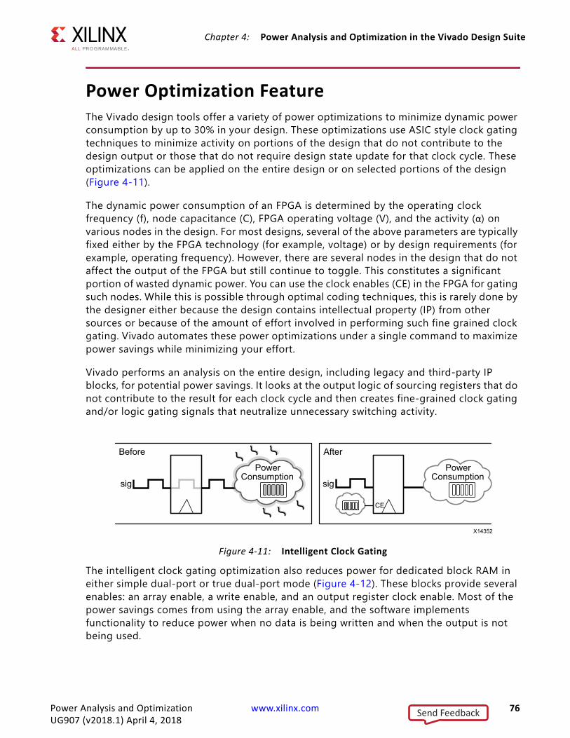
Chapter 4: Power Analysis and Optimization in the Vivado Design Suite
Power Optimization FeatureThe Vivado design tools offer a variety of power optimizations to minimize dynamic power consumption by up to 30% in your design. These optimizations use ASIC style clock gating techniques to minimize activity on portions of the design that do not contribute to the design output or those that do not require design state update for that clock cycle. These optimizations can be applied on the entire design or on selected portions of the design (Figure 4-11).
The dynamic power consumption of an FPGA is determined by the operating clock frequency (f), node capacitance (C), FPGA operating voltage (V), and the activity (α) on various nodes in the design. For most designs, several of the above parameters are typically fixed either by the FPGA technology (for example, voltage) or by design requirements (for example, operating frequency). However, there are several nodes in the design that do not affect the output of the FPGA but still continue to toggle. This constitutes a significant portion of wasted dynamic power. You can use the clock enables (CE) in the FPGA for gating such nodes. While this is possible through optimal coding techniques, this is rarely done by the designer either because the design contains intellectual property (IP) from other sources or because of the amount of effort involved in performing such fine grained clock gating. Vivado automates these power optimizations under a single command to maximize power savings while minimizing your effort.
Vivado performs an analysis on the entire design, including legacy and third-party IP blocks, for potential power savings. It looks at the output logic of sourcing registers that do not contribute to the result for each clock cycle and then creates fine-grained clock gating and/or logic gating signals that neutralize unnecessary switching activity.
The intelligent clock gating optimization also reduces power for dedicated block RAM in either simple dual-port or true dual-port mode (Figure 4-12). These blocks provide several enables: an array enable, a write enable, and an output register clock enable. Most of the power savings comes from using the array enable, and the software implements functionality to reduce power when no data is being written and when the output is not being used.
X-Ref Target - Figure 4-11
Figure 4-11: Intelligent Clock Gating
sig sig
Power Consumption
CE
AfterBefore
X14352
Power Consumption
Power Analysis and Optimization www.xilinx.com 76UG907 (v2018.1) April 4, 2018
Send Feedback

Chapter 4: Power Analysis and Optimization in the Vivado Design Suite
Xilinx intelligent clock gating optimizations do not modify user logic but instead create additional gating logic. Therefore the functionality of the design is preserved at all times. However, this optimization could impact timing, especially if the optimization is applied on critical paths.
Block RAM WRITE_MODE Power Optimizations
In Xilinx 7 series devices, for Block RAMs in true dual port (TDP) mode, the WRITE_MODE can be changed from WRITE_FIRST to NO_CHANGE safely if the output of that port is not connected or the corresponding output is not needed during write operation.
Similarly, for BRAM in true dual port (TDP) mode, the WRITE_MODE can be changed from READ_FIRST to NO_CHANGE safely if the corresponding output port is not connected.
In UltraScale™ devices, in addition to the above optimization, for Block RAM in Simple Dual Port (SDP) mode, WRITE_MODE of both the read and write ports can be changed to NO_CHANGE safely if the read and write port clocks are asynchronous.
These changes help to save power in the write cycle by not updating the output port of the BRAM. This optimization will be performed only when there is no impact to user defined functionality and performance.
Block RAM Cascade Optimizations
In Xilinx 7 series devices, if BRAMs are found to be cascaded, since only one BRAM can be active at any time, the rest of the BRAMs can be disabled based on address and any existing enable conditions. This enables large power savings.
These optimizations are performed by default in the opt_design phase in the Vivado Design Suite.
X-Ref Target - Figure 4-12
Figure 4-12: Clock Gating Optimizations Using Block RAM Enables
address address
data in
data in
ce
data outdata out
AfterBefore
WP389_16_021011
Power Analysis and Optimization www.xilinx.com 77UG907 (v2018.1) April 4, 2018
Send Feedback
Chapter 4: Power Analysis and Optimization in the Vivado Design Suite
Performing Power Optimization in the Vivado IDEPower optimizations are performed during two stages in Vivado: opt_design and power_opt_design.
Optimizations that are performed during the opt_design phase occur without user intervention. These optimizations primarily focus on power savings on Block RAMs.
IMPORTANT: The power optimization might impact the timing performance of your design during opt_design, power_opt_design, or both.
For UltraScale devices, the more aggressive BRAM power optimizations that may negatively impact timing are included only in power_opt_design. This allows performance to be traded for power savings. For UltraScale+ devices, XPM-URAM power optimization occurs in power_opt_design.
By default the opt_design command will perform BRAM power optimization. BRAM power optimization can also be run explicitly and standalone by using the -bram_power_opt option:
opt_design -bram_power_opt
To disable BRAM power optimization from the default opt_design flow, set the NoBramPowerOpt directive to the opt_design command:
opt_design -directive NoBramPowerOpt
You can also set this directive in the Implementation settings window as shown in Figure 4-13 below.
Power Analysis and Optimization www.xilinx.com 78UG907 (v2018.1) April 4, 2018
Send Feedback
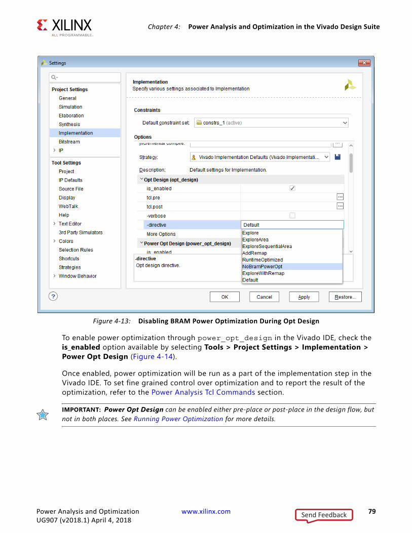
Chapter 4: Power Analysis and Optimization in the Vivado Design Suite
To enable power optimization through power_opt_design in the Vivado IDE, check the is_enabled option available by selecting Tools > Project Settings > Implementation > Power Opt Design (Figure 4-14).
Once enabled, power optimization will be run as a part of the implementation step in the Vivado IDE. To set fine grained control over optimization and to report the result of the optimization, refer to the Power Analysis Tcl Commands section.
IMPORTANT: Power Opt Design can be enabled either pre-place or post-place in the design flow, but not in both places. See Running Power Optimization for more details.
X-Ref Target - Figure 4-13
Figure 4-13: Disabling BRAM Power Optimization During Opt Design
Power Analysis and Optimization www.xilinx.com 79UG907 (v2018.1) April 4, 2018
Send Feedback
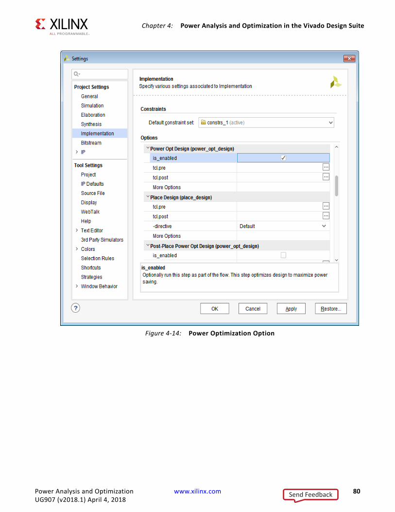
Chapter 4: Power Analysis and Optimization in the Vivado Design Suite
X-Ref Target - Figure 4-14
Figure 4-14: Power Optimization Option
Power Analysis and Optimization www.xilinx.com 80UG907 (v2018.1) April 4, 2018
Send Feedback

Chapter 4: Power Analysis and Optimization in the Vivado Design Suite
Displaying a Power Optimization Report in the Vivado IDEIn the Vivado IDE you can display a power optimization report that describes the power optimizations that have been performed on your design. You can display the power optimization report after synthesis or after implementation.
IMPORTANT: In Vivado, power optimization is performed during the opt_design and power_opt_design stages of the Vivado design flow. Both of these stages occur during implementation, which occurs after the design has been synthesized. If you generate a power optimization report on the synthesized design, the report will only contain information about the power optimization features that were coded into your original design (for example, gating a BRAM using a clock enable (CE)). The report will not detail power optimizations performed later by the tools, during implementation.
To display a Power Optimization Report in the Vivado IDE:
1. In the Flow Navigator, select Open Synthesized Design or Open Implemented Design.2. Select Reports > Report Power Optimization.
The equivalent Tcl command to perform this operation is:
report_power_opt -name <report_name>
3. In the Report Power Optimization dialog box (Figure 4-15), specify the following options.
° Results name: Specify the name under which the power optimization report will appear in the Vivado IDE.
° Export to file: Check this box to generate a text report in addition to the power optimization report in the Vivado IDE. Specify a file name and location for the text report, and select whether this will be a TXT or XML file.
° Open in a new tab: Check this box to add this new power optimization report to any other power optimization reports currently displayed in the Vivado IDE. Leave this box unchecked to replace any power optimization reports currently displayed in the Vivado IDE with this new power optimization report.
Power Analysis and Optimization www.xilinx.com 81UG907 (v2018.1) April 4, 2018
Send Feedback
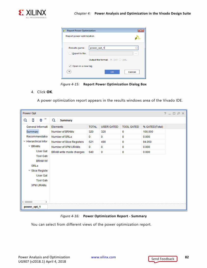
Chapter 4: Power Analysis and Optimization in the Vivado Design Suite
4. Click OK.
A power optimization report appears in the results windows area of the Vivado IDE.
You can select from different views of the power optimization report.
X-Ref Target - Figure 4-15
Figure 4-15: Report Power Optimization Dialog Box
X-Ref Target - Figure 4-16
Figure 4-16: Power Optimization Report - Summary
Power Analysis and Optimization www.xilinx.com 82UG907 (v2018.1) April 4, 2018
Send Feedback
Chapter 4: Power Analysis and Optimization in the Vivado Design Suite
• General Information: Information about your design, the Xilinx device into which your design will be implemented, and the Tcl command that generated this power optimization report.
• Summary: Count of BRAMs, SRLs and Slice Registers that were optimized by the user in the design and by the power optimization tool.
• Recommendations: Things you can do to further optimize your design for power.• Hierarchical Information: Details of the BRAMs, SRLs, and Slice Registers for which
Vivado has performed power optimization.
For a description of the power optimizations Vivado performs, see Power Optimization Feature and Block RAM WRITE_MODE Power Optimizations.
sd TIP: If any hierarchical module or instance is tagged with a DONT_TOUCH attribute, Power Optimization will not optimize this logic.
Performing Power Optimization Using the Tcl InterfaceThere are four power optimization Tcl commands in Vivado:
• set_power_opt
• opt_design -bram_power_opt
• power_opt_design
• report_power_opt
These commands can be used to enable power optimization as well as control portions of the design that are to be optimized, and to generate a report that shows the effect of the optimizations performed.
For information on options, properties, applicable elements, or returned values for a specific command:
• Type <command_name> -help• See the Vivado Design Suite Tcl Command Reference Guide (UG835) [Ref 2] and the
Vivado Design Suite User Guide: Using Constraints (UG903) [Ref 3]
Power Analysis and Optimization www.xilinx.com 83UG907 (v2018.1) April 4, 2018
Send Feedback
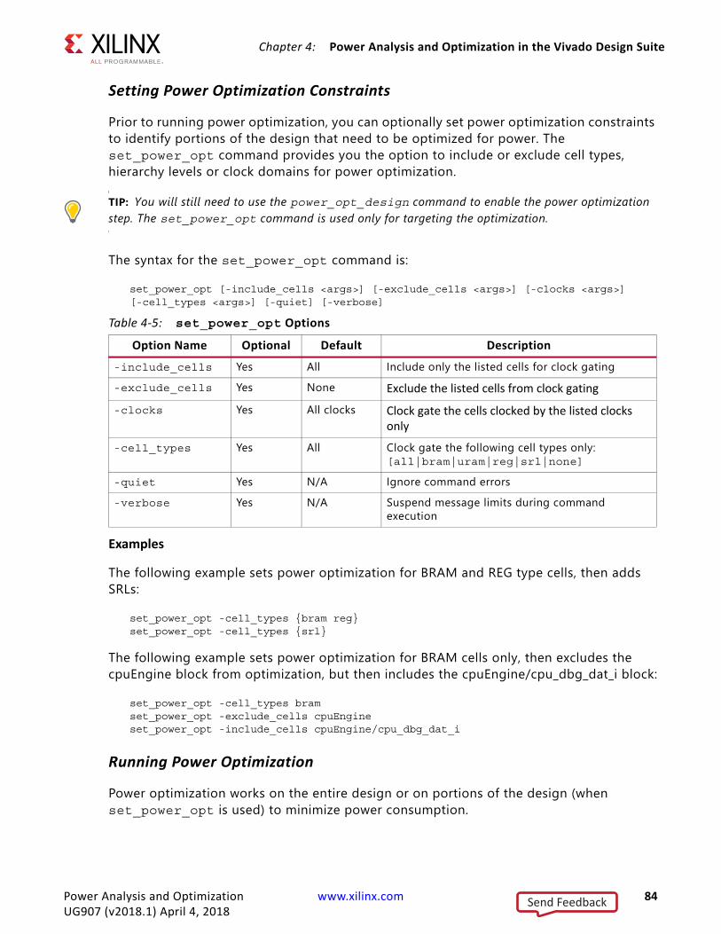
Chapter 4: Power Analysis and Optimization in the Vivado Design Suite
Setting Power Optimization Constraints
Prior to running power optimization, you can optionally set power optimization constraints to identify portions of the design that need to be optimized for power. The set_power_opt command provides you the option to include or exclude cell types, hierarchy levels or clock domains for power optimization.
TIP: You will still need to use the power_opt_design command to enable the power optimization step. The set_power_opt command is used only for targeting the optimization.
The syntax for the set_power_opt command is:
set_power_opt [-include_cells <args>] [-exclude_cells <args>] [-clocks <args>] [-cell_types <args>] [-quiet] [-verbose]
Examples
The following example sets power optimization for BRAM and REG type cells, then adds SRLs:
set_power_opt -cell_types {bram reg}set_power_opt -cell_types {srl}
The following example sets power optimization for BRAM cells only, then excludes the cpuEngine block from optimization, but then includes the cpuEngine/cpu_dbg_dat_i block:
set_power_opt -cell_types bramset_power_opt -exclude_cells cpuEngineset_power_opt -include_cells cpuEngine/cpu_dbg_dat_i
Running Power Optimization
Power optimization works on the entire design or on portions of the design (when set_power_opt is used) to minimize power consumption.
Table 4-5: set_power_opt OptionsOption Name Optional Default Description
-include_cells Yes All Include only the listed cells for clock gating-exclude_cells Yes None Exclude the listed cells from clock gating-clocks Yes All clocks Clock gate the cells clocked by the listed clocks
only-cell_types Yes All Clock gate the following cell types only:
[all|bram|uram|reg|srl|none]
-quiet Yes N/A Ignore command errors-verbose Yes N/A Suspend message limits during command
execution
Power Analysis and Optimization www.xilinx.com 84UG907 (v2018.1) April 4, 2018
Send Feedback
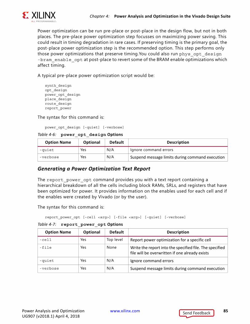
Chapter 4: Power Analysis and Optimization in the Vivado Design Suite
Power optimization can be run pre-place or post-place in the design flow, but not in both places. The pre-place power optimization step focusses on maximizing power saving. This could result in timing degradation in rare cases. If preserving timing is the primary goal, the post-place power optimization step is the recommended option. This step performs only those power optimizations that preserve timing.You could also run phys_opt_design -bram_enable_opt at post-place to revert some of the BRAM enable optimizations which affect timing.
A typical pre-place power optimization script would be:
synth_designopt_designpower_opt_designplace_designroute_designreport_power
The syntax for this command is:
power_opt_design [-quiet] [-verbose]
Generating a Power Optimization Text Report
The report_power_opt command provides you with a text report containing a hierarchical breakdown of all the cells including block RAMs, SRLs, and registers that have been optimized for power. It provides information on the enables used for each cell and if the enables were created by Vivado (or by the user).
The syntax for this command is:
report_power_opt [-cell <arg>] [-file <arg>] [-quiet] [-verbose]
Table 4-6: power_opt_design OptionsOption Name Optional Default Description
-quiet Yes N/A Ignore command errors-verbose Yes N/A Suspend message limits during command execution
Table 4-7: report_power_opt OptionsOption Name Optional Default Description
-cell Yes Top level Report power optimization for a specific cell-file Yes None Write the report into the specified file. The specified
file will be overwritten if one already exists-quiet Yes N/A Ignore command errors-verbose Yes N/A Suspend message limits during command execution
Power Analysis and Optimization www.xilinx.com 85UG907 (v2018.1) April 4, 2018
Send Feedback

Chapter 4: Power Analysis and Optimization in the Vivado Design Suite
Examples
The following example creates a file named myopt.rep and reports power optimization for the entire design:
report_power_opt -file myopt.rep
The following example creates a file named myopt.rep and reports power optimization for the mctrl0 sub-hierarchy of the design:
report_power_opt -file myopt2.rep -cell mcore0/mctrl0
Guidelines to Maximize Power Saving with Power OptimizationTo maximize power savings when you run power optimization in the Vivado tools, you should run power optimization on the entire design and not exclude portions of the design. If you do not see anticipated power savings after enabling power optimization, make sure the design is properly constrained. Check to see if all registers in the design have been constrained, using the check_timing command.
If the design has been constrained correctly, then review the design for potential coding styles that could impact power optimizations. The three areas of potential debug are the global set and reset signals, block RAM enable generation, and register clock gating. A low number of power optimization generated enables could indicate the need to review coding practices or options/properties set for design synthesis and implementation.
• Global set and reset signals
Where possible, minimize the use of asynchronous set/reset signals especially to datapath or pipeline flip-flops as well as block RAMs (BRAM).
You should also consider constraining the global set and reset signals as dont_touch during the power_opt_design step to avoid their use as enables. Note that setting dont_touch property in HDL will cause every step in the flow to obey this property. It is recommended that this option is set up as an XDC constraint only for the power optimization step. Here is an example of how to do this:
set_property DONT_TOUCH true [get_cells u1]
Finally, ensure that the signal rate and probabilities of the global set and reset signals are set correctly prior to running power optimization and vectorless power estimation.
Power Analysis and Optimization www.xilinx.com 86UG907 (v2018.1) April 4, 2018
Send Feedback

Chapter 4: Power Analysis and Optimization in the Vivado Design Suite
• Slice registers and SRLs
A number of different reasons could explain why power_opt_design might not be able to generate clock enables for slice registers or SRLs in the design. Some examples are:
° Having combinatorial loops in the design
° Using set/reset signals at the flip-flops and SRLs that are sourced from primary inputs to the design
° Using asynchronous set/reset signals at the datapath flip-flops
° Large number of clock domains in the design preventing enables being generated due to clock domain crossing issues
° SRL sizes: Typically the larger the number of shift register stages in the SRLs, the more difficult it is to generate a single clock enable for all stages
• Block RAMs
Block RAM (BRAM) rich designs are excellent candidates for power savings. Vivado uses a variety of optimization techniques to generate enables and save power. If BRAM gating coverage is low after using power_opt_design, some of the possible reasons could be:
° BRAMs are mainly FIFO18/FIFO36 cells. These cannot be optimized by the tool.
° Memories inferred or instantiated are mainly in true dual port (TDP) mode using asynchronous clocks on their A and B ports that cannot be optimized by power_opt_design.
° Use of asynchronous reset signals to either the BRAM themselves or to the address/write-enable flip-flops feeding the BRAMs.
Preserving Timing After Power Optimization
Power optimization works to minimize the impact on timing while maximizing power savings. However, in certain cases, if timing degrades after power optimization, you can employ a few techniques to offset this impact.
Where possible, identify and apply power optimizations only on non-timing critical clock domains or modules using the set_power_opt XDC command. If the most critical clock domain happens to cover a large portion of the design or consumes the most power, review critical paths to see if any cells in the critical path were optimized by power optimization. Note that objects optimized by power optimization have an IS_CLOCK_GATED property on them. Exclude these cells from power optimization.
Power Analysis and Optimization www.xilinx.com 87UG907 (v2018.1) April 4, 2018
Send Feedback
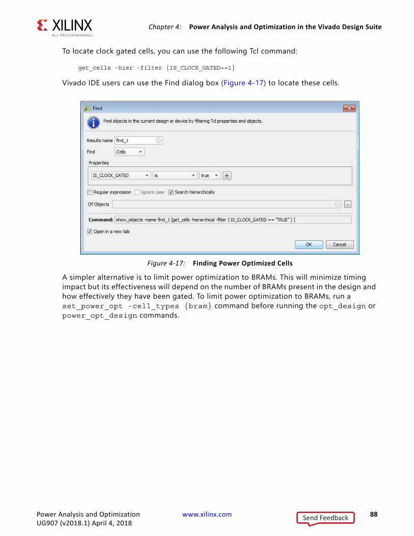
Chapter 4: Power Analysis and Optimization in the Vivado Design Suite
To locate clock gated cells, you can use the following Tcl command:
get_cells -hier -filter {IS_CLOCK_GATED==1}
Vivado IDE users can use the Find dialog box (Figure 4-17) to locate these cells.
A simpler alternative is to limit power optimization to BRAMs. This will minimize timing impact but its effectiveness will depend on the number of BRAMs present in the design and how effectively they have been gated. To limit power optimization to BRAMs, run a set_power_opt -cell_types {bram} command before running the opt_design or power_opt_design commands.
X-Ref Target - Figure 4-17
Figure 4-17: Finding Power Optimized Cells
Power Analysis and Optimization www.xilinx.com 88UG907 (v2018.1) April 4, 2018
Send Feedback
Chapter 5
Achieving an Accurate Power Analysis Using Vivado Report Power
IntroductionAn accurate power estimation is always challenging for the software tools, since the tools have to assume various factors on their own. If you can guide the tool as much as possible to minimize these assumptions, you can achieve a more accurate power estimation.
For an accurate power analysis, the following factors must be considered:
• Thermal settings• Power Supply settings• Clock specifications• Control Signals• Primary Inputs• Individual components
Thermal SettingsIdeally, static power is the sum of source to drain and gate leakage power in the transistor. Static power is purely dependent on Thermal conditions. Providing more accurate thermal information is a basic requirement for accurate power estimation.
Power Analysis and Optimization www.xilinx.com 89UG907 (v2018.1) April 4, 2018
Send Feedback
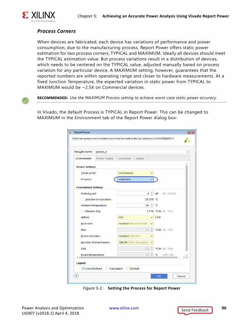
Chapter 5: Achieving an Accurate Power Analysis Using Vivado Report Power
Process Corners
When devices are fabricated, each device has variations of performance and power consumption, due to the manufacturing process. Report Power offers static power estimation for two process corners, TYPICAL and MAXIMUM. Ideally all devices should meet the TYPICAL estimation value. But process variations result in a distribution of devices, which needs to be centered on the TYPICAL value, adjusted manually based on process variation for any particular device. A MAXIMUM setting, however, guarantees that the reported numbers are within operating range and closer to hardware measurements. At a fixed Junction Temperature, the expected variation in static power from TYPICAL to MAXIMUM would be ~2.5X on Commercial devices.
RECOMMENDED: Use the MAXIMUM Process setting to achieve worst-case static power accuracy.
In Vivado, the default Process is TYPICAL in Report Power. This can be changed to MAXIMUM in the Environment tab of the Report Power dialog box:X-Ref Target - Figure 5-1
Figure 5-1: Setting the Process for Report Power
Power Analysis and Optimization www.xilinx.com 90UG907 (v2018.1) April 4, 2018
Send Feedback
Chapter 5: Achieving an Accurate Power Analysis Using Vivado Report Power
Equivalent Tcl command:
set_operating_conditions -process maximum
Junction Temperature
Leakage current increases exponentially with Junction Temperature, which results in higher static power. Junction Temperature depends on various factors: the total power of the device, the cooling system, board selection, and ambient conditions. By default the Junction Temperature is computed based on other Thermal setup inputs: Ambient Temperature, Heat Sink, Board Selection, etc. Since Junction Temperature is directly proportional to total power, it varies when dynamic power increases. It is very important to specify the right Junction Temperature to estimate accurate static power.
RECOMMENDED: Read the Junction Temperature at the time when power is measured on the hardware and overwrite the existing setting in the Report Power dialog box.
To set Junction Temperature in the Vivado IDE, enable the Junction Temperature check box in the Environment tab of the Report Power dialog box and enter the value.
Power Analysis and Optimization www.xilinx.com 91UG907 (v2018.1) April 4, 2018
Send Feedback
Chapter 5: Achieving an Accurate Power Analysis Using Vivado Report Power
Equivalent Tcl command:
set_operating_conditions -junction_temp 45
You can measure approximate Junction Temperature by placing a simple thermistor or other hand-held temperature measurement device on the Xilinx device. If one of the Xilinx Hardware Programing tools is used to program the devices, then you can read the Die Temperature values. For example, ISE-Impact reads Die Temperature values when you select
X-Ref Target - Figure 5-2
Figure 5-2: Setting Junction Temperature for Report Power
Power Analysis and Optimization www.xilinx.com 92UG907 (v2018.1) April 4, 2018
Send Feedback

Chapter 5: Achieving an Accurate Power Analysis Using Vivado Report Power
Debug > Read Status Register. Vivado Hardware Manager graphically drafts the Die Temperature plots in the System Monitor Window.
Power Supply SettingsVoltage scaling is one of the prominent power saving approaches in Xilinx FPGAs and All Programmable SOCs. There are different voltage rails to supply specific voltages to logic in the device. Each Device Data Sheet lists the recommended operating conditions of these rails. For example, Kintex7 devices can operate with a VCCINT rail between 0.97V and 1.03V. You can make use of voltage scaling to meet your power budget. In the Hardware setup, these rails are supplied by external Power Regulators with fine-grained controls. Since power increases when supply voltage increases, you must provide the exact supply voltage to estimate power accurately.
RECOMMENDED: Specify accurate power supply values in the Power Supply tab of the Report Power dialog box.
To specify power supply voltages in the Vivado IDE, enter the values in the Power Supply tab of the Report Power dialog box.
Power Analysis and Optimization www.xilinx.com 93UG907 (v2018.1) April 4, 2018
Send Feedback
Chapter 5: Achieving an Accurate Power Analysis Using Vivado Report Power
Equivalent Tcl command:
set_operating_conditions -voltage {vccint 0.98 vccaux 1.8}
Clock SpecificationsDesign clocks are the main component for dynamic power computation. If no clocks are defined, switching activity estimates will be inaccurate, resulting in inaccurate power
X-Ref Target - Figure 5-3
Figure 5-3: Setting Power Supply Values for Report Power
Power Analysis and Optimization www.xilinx.com 94UG907 (v2018.1) April 4, 2018
Send Feedback

Chapter 5: Achieving an Accurate Power Analysis Using Vivado Report Power
estimates. A clock node is identified from timing constraints which are defined using create_clock or create_generated_clock XDC commands.
RECOMMENDED: All the required clocks in the design must be defined using create_clock or create_generated_clock commands.
Power Analysis and Optimization www.xilinx.com 95UG907 (v2018.1) April 4, 2018
Send Feedback
Chapter 5: Achieving an Accurate Power Analysis Using Vivado Report Power
The Switching tab of the Report Power dialog box displays all the clocks defined in the design.
X-Ref Target - Figure 5-4
Figure 5-4: Constrained Clocks for Report Power
Power Analysis and Optimization www.xilinx.com 96UG907 (v2018.1) April 4, 2018
Send Feedback
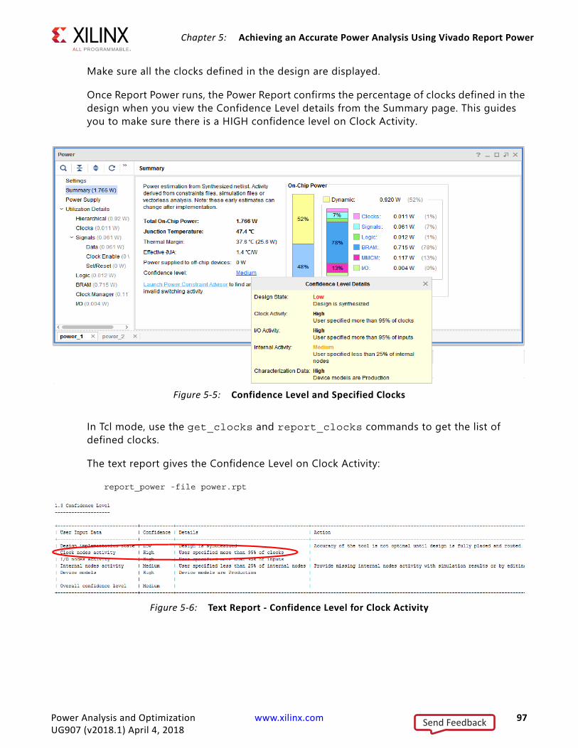
Chapter 5: Achieving an Accurate Power Analysis Using Vivado Report Power
Make sure all the clocks defined in the design are displayed.
Once Report Power runs, the Power Report confirms the percentage of clocks defined in the design when you view the Confidence Level details from the Summary page. This guides you to make sure there is a HIGH confidence level on Clock Activity.
In Tcl mode, use the get_clocks and report_clocks commands to get the list of defined clocks.
The text report gives the Confidence Level on Clock Activity:
report_power -file power.rpt
X-Ref Target - Figure 5-5
Figure 5-5: Confidence Level and Specified Clocks
X-Ref Target - Figure 5-6
Figure 5-6: Text Report - Confidence Level for Clock Activity
Power Analysis and Optimization www.xilinx.com 97UG907 (v2018.1) April 4, 2018
Send Feedback

Chapter 5: Achieving an Accurate Power Analysis Using Vivado Report Power
Control Signals
Global and Regional Resets
The Activity rate on Global Resets could change the power estimation dramatically. It conveys the state of each logic block in the design and the probability of logic output changes. If it is not set with the right switching information, you can get unrealistic power estimates.
For example, ideally Reset is expected to be asserted (active) at the beginning of the run for a few cycles and remains inactive the rest of the time.
This could be denoted in terms of switching activity as:
set_switching_activity -static_probability 0.01 -signal_rate 2 [get_ports glb_reset]
Report Power identifies primary ports which are found to be global resets and applies the above switching activity. It uses a very conservative and safe way to identify the global resets - the ports which are directly connected to Reset pins of leaf primitives.
However this does not help much on complex designs where the Reset logic is generated internally through special logic circuits (reset generator, debouncer, reset stretching, etc). When there is logic involved to generate Reset, Report Power is not aware of design intent and does not apply any default switching information on it.
X-Ref Target - Figure 5-7
Figure 5-7: Reset Signal Duration
X-Ref Target - Figure 5-8
Figure 5-8: Reset Logic
MMCMClk_reset_gen
MMCMLock user_reset
X14354
Power Analysis and Optimization www.xilinx.com 98UG907 (v2018.1) April 4, 2018
Send Feedback
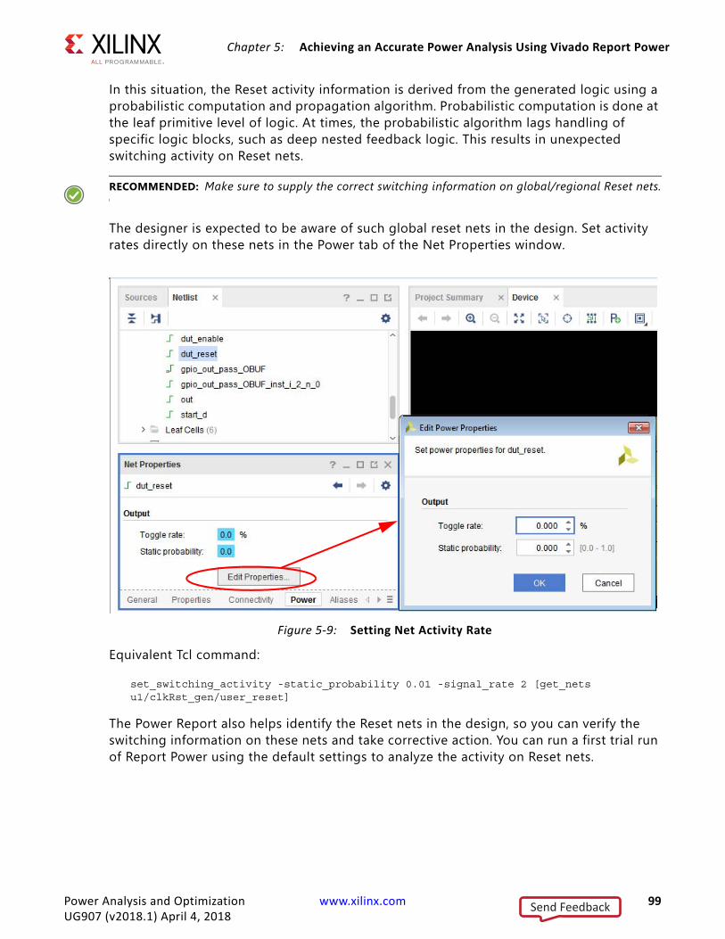
Chapter 5: Achieving an Accurate Power Analysis Using Vivado Report Power
In this situation, the Reset activity information is derived from the generated logic using a probabilistic computation and propagation algorithm. Probabilistic computation is done at the leaf primitive level of logic. At times, the probabilistic algorithm lags handling of specific logic blocks, such as deep nested feedback logic. This results in unexpected switching activity on Reset nets.
RECOMMENDED: Make sure to supply the correct switching information on global/regional Reset nets.
The designer is expected to be aware of such global reset nets in the design. Set activity rates directly on these nets in the Power tab of the Net Properties window.
Equivalent Tcl command:
set_switching_activity -static_probability 0.01 -signal_rate 2 [get_nets u1/clkRst_gen/user_reset]
The Power Report also helps identify the Reset nets in the design, so you can verify the switching information on these nets and take corrective action. You can run a first trial run of Report Power using the default settings to analyze the activity on Reset nets.
X-Ref Target - Figure 5-9
Figure 5-9: Setting Net Activity Rate
Power Analysis and Optimization www.xilinx.com 99UG907 (v2018.1) April 4, 2018
Send Feedback
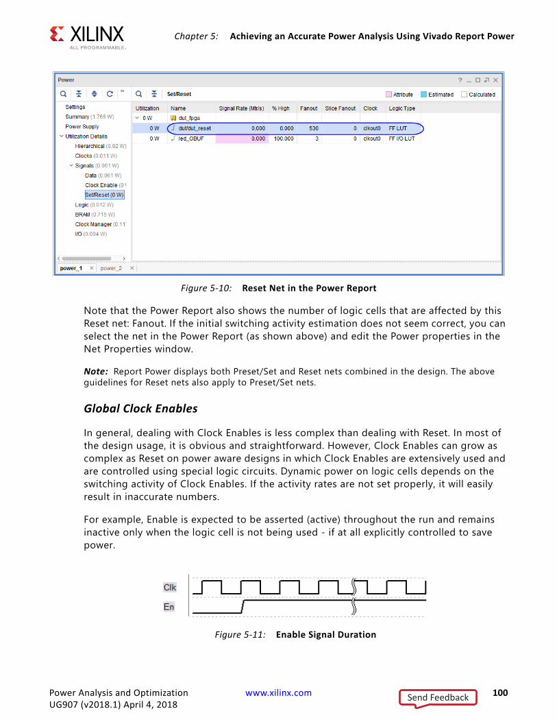
Chapter 5: Achieving an Accurate Power Analysis Using Vivado Report Power
Note that the Power Report also shows the number of logic cells that are affected by this Reset net: Fanout. If the initial switching activity estimation does not seem correct, you can select the net in the Power Report (as shown above) and edit the Power properties in the Net Properties window.
Note: Report Power displays both Preset/Set and Reset nets combined in the design. The above guidelines for Reset nets also apply to Preset/Set nets.
Global Clock Enables
In general, dealing with Clock Enables is less complex than dealing with Reset. In most of the design usage, it is obvious and straightforward. However, Clock Enables can grow as complex as Reset on power aware designs in which Clock Enables are extensively used and are controlled using special logic circuits. Dynamic power on logic cells depends on the switching activity of Clock Enables. If the activity rates are not set properly, it will easily result in inaccurate numbers.
For example, Enable is expected to be asserted (active) throughout the run and remains inactive only when the logic cell is not being used - if at all explicitly controlled to save power.
X-Ref Target - Figure 5-10
Figure 5-10: Reset Net in the Power Report
X-Ref Target - Figure 5-11
Figure 5-11: Enable Signal Duration
Power Analysis and Optimization www.xilinx.com 100UG907 (v2018.1) April 4, 2018
Send Feedback
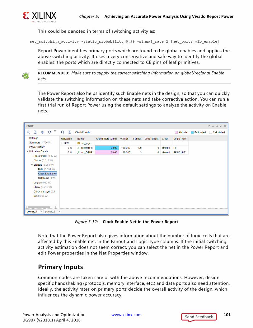
Chapter 5: Achieving an Accurate Power Analysis Using Vivado Report Power
This could be denoted in terms of switching activity as:
set_switching_activity -static_probability 0.99 -signal_rate 2 [get_ports glb_enable]
Report Power identifies primary ports which are found to be global enables and applies the above switching activity. It uses a very conservative and safe way to identify the global enables: the ports which are directly connected to CE pins of leaf primitives.
RECOMMENDED: Make sure to supply the correct switching information on global/regional Enable nets.
The Power Report also helps identify such Enable nets in the design, so that you can quickly validate the switching information on these nets and take corrective action. You can run a first trial run of Report Power using the default settings to analyze the activity on Enable nets.
Note that the Power Report also gives information about the number of logic cells that are affected by this Enable net, in the Fanout and Logic Type columns. If the initial switching activity estimation does not seem correct, you can select the net in the Power Report and edit Power properties in the Net Properties window.
Primary InputsCommon nodes are taken care of with the above recommendations. However, design specific handshaking (protocols, memory interface, etc.) and data ports also need attention. Ideally, the activity rates on primary ports decide the overall activity of the design, which influences the dynamic power accuracy.
X-Ref Target - Figure 5-12
Figure 5-12: Clock Enable Net in the Power Report
Power Analysis and Optimization www.xilinx.com 101UG907 (v2018.1) April 4, 2018
Send Feedback
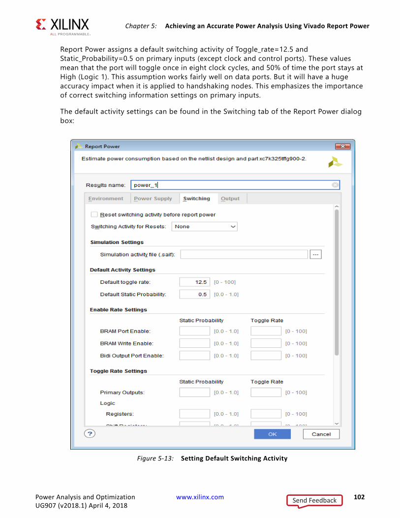
Chapter 5: Achieving an Accurate Power Analysis Using Vivado Report Power
Report Power assigns a default switching activity of Toggle_rate=12.5 and Static_Probability=0.5 on primary inputs (except clock and control ports). These values mean that the port will toggle once in eight clock cycles, and 50% of time the port stays at High (Logic 1). This assumption works fairly well on data ports. But it will have a huge accuracy impact when it is applied to handshaking nodes. This emphasizes the importance of correct switching information settings on primary inputs.
The default activity settings can be found in the Switching tab of the Report Power dialog box:X-Ref Target - Figure 5-13
Figure 5-13: Setting Default Switching Activity
Power Analysis and Optimization www.xilinx.com 102UG907 (v2018.1) April 4, 2018
Send Feedback
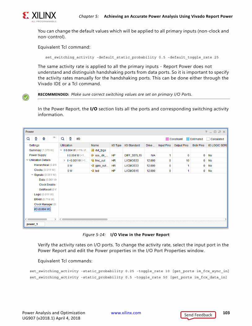
Chapter 5: Achieving an Accurate Power Analysis Using Vivado Report Power
You can change the default values which will be applied to all primary inputs (non-clock and non-control).
Equivalent Tcl command:
set_switching_activity -default_static_probability 0.5 -default_toggle_rate 25
The same activity rate is applied to all the primary inputs - Report Power does not understand and distinguish handshaking ports from data ports. So it is important to specify the activity rates manually for the handshaking ports. This can be done either through the Vivado IDE or a Tcl command.
RECOMMENDED: Make sure correct switching values are set on primary I/O Ports.
In the Power Report, the I/O section lists all the ports and corresponding switching activity information.
Verify the activity rates on I/O ports. To change the activity rate, select the input port in the Power Report and edit the Power properties in the I/O Port Properties window.
Equivalent Tcl commands:
set_switching_activity -static_probability 0.25 -toggle_rate 10 [get_ports im_fcx_sync_in]
set_switching_activity -static_probability 0.5 -toggle_rate 50 [get_ports im_fcx_data_in]
X-Ref Target - Figure 5-14
Figure 5-14: I/O View in the Power Report
Power Analysis and Optimization www.xilinx.com 103UG907 (v2018.1) April 4, 2018
Send Feedback
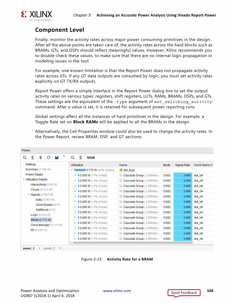
Chapter 5: Achieving an Accurate Power Analysis Using Vivado Report Power
Component LevelFinally, monitor the activity rates across major power consuming primitives in the design. After all the above points are taken care of, the activity rates across the hard blocks such as BRAMs, GTs, and DSPs should reflect meaningful values. However, Xilinx recommends you to double-check these values, to make sure that there are no internal logic propagation or modeling issues in the tool.
For example, one known limitation is that the Report Power does not propagate activity rates across GTs. If any GT data outputs are consumed by logic, you must set activity rates explicitly on GT TX/RX outputs.
Report Power offers a simple interface in the Report Power dialog box to set the output activity rates on various types: registers, shift registers, LUTs, RAMs, BRAMs, DSPs, and GTs. These settings are the equivalent of the -type argument of set_switching_activity command. After a value is set, it is retained for subsequent power reporting runs.
Global settings affect all the instances of hard primitives in the design. For example, a Toggle Rate set on Block RAMs will be applied to all the BRAMs in the design.
Alternatively, the Cell Properties window could also be used to change the activity rates. In the Power Report, review BRAM, DSP, and GT sections:
X-Ref Target - Figure 5-15
Figure 5-15: Activity Rate for a BRAM
Power Analysis and Optimization www.xilinx.com 104UG907 (v2018.1) April 4, 2018
Send Feedback
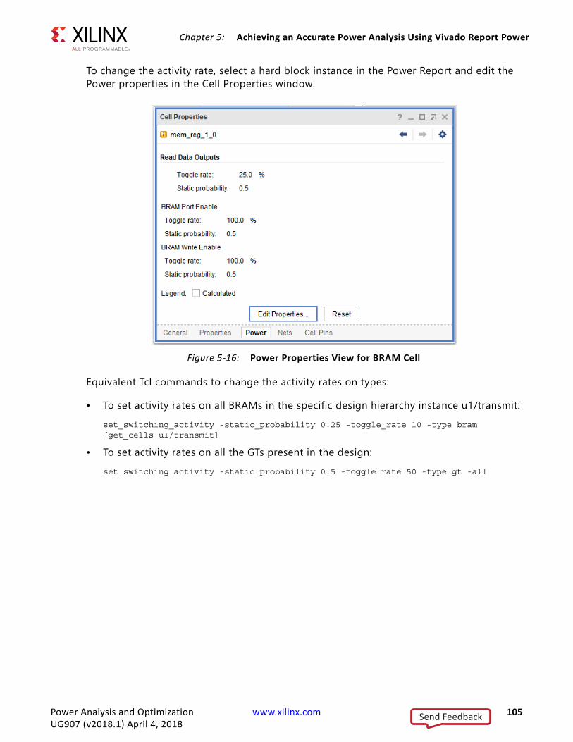
Chapter 5: Achieving an Accurate Power Analysis Using Vivado Report Power
To change the activity rate, select a hard block instance in the Power Report and edit the Power properties in the Cell Properties window.
Equivalent Tcl commands to change the activity rates on types:
• To set activity rates on all BRAMs in the specific design hierarchy instance u1/transmit:set_switching_activity -static_probability 0.25 -toggle_rate 10 -type bram [get_cells u1/transmit]
• To set activity rates on all the GTs present in the design:set_switching_activity -static_probability 0.5 -toggle_rate 50 -type gt -all
X-Ref Target - Figure 5-16
Figure 5-16: Power Properties View for BRAM Cell
Power Analysis and Optimization www.xilinx.com 105UG907 (v2018.1) April 4, 2018
Send Feedback

Chapter 6
Tips and Techniques for Power Reduction
IntroductionThis chapter describes power reduction techniques and their expected effect on total device power. This information will help you evaluate your best options depending on your time, power budget, available resources, and freedom to change your design.
System-Level Power ReductionCooling StrategyCooling strategy ensures that heat generated from the device is extracted and absorbed by the environment. These cooling strategies, which are generally available at the beginning of the design and become less feasible in the later stages, have a significant impact on the device static power:
• Increase the airflow.• Lower the ambient temperature.• Use a heat sink (or a larger heat sink), or select a different regulator.
Supply StrategyVoltage has a large effect on both static and dynamic power. Active control of the voltage level ensures the desired voltage is applied to the device.
• Use switching regulators.
Switching regulators are more power efficient than linear regulators, at the expense of requiring a higher component count.
Power Analysis and Optimization www.xilinx.com 106UG907 (v2018.1) April 4, 2018
Send Feedback

Chapter 6: Tips and Techniques for Power Reduction
• Use adjustable regulators.
Sense voltage as close as possible to the FPGA and to the highest consuming device if the same supply powers multiple FPGAs.
• Select regulators with tight tolerances.
Device Selection• Select the best device for the product.
Increasingly, power is becoming one of the primary factors for selecting a device. Select the device that best meets your density, functionality, and performance requirements and will also meet your power budget.
• Minimize the number of devices.
This saves space, I/O interconnect power, total leakage, and other factors. Typically, replacing multiple components (for example, processor and FPGA) with a single larger FPGA consumes less static power.
• Select the smallest device possible.
This reduces leakage. Typically in an FPGA family the same package may be available with different die sizes. You can, for instance, use a larger die during the prototyping and pre-series phase, then move to a smaller die for volume production.
• Select the largest package possible.
This increases heat dissipation. A larger package has a larger area to dissipate the die heat into the environment. A larger heat sink can be attached to the package upper side and more heat can escape onto the PCB via the bottom ball grid array.
• Use low voltage devices.
Some device families are available with a lower power option. The lower core voltage requirements translate into significant static and dynamic power savings.
• Use low leakage devices.
Some device families are available with a lower leakage or static power options in the form of specific speed or temperature grades. These devices may cost a bit more to purchase but you or the end user may be able to more than offset this with savings on the electricity bill or cooling hardware and system maintenance.
Power Analysis and Optimization www.xilinx.com 107UG907 (v2018.1) April 4, 2018
Send Feedback

Chapter 6: Tips and Techniques for Power Reduction
Measuring Power and TemperatureThis section describes the techniques for measuring FPGA device power consumption and heat dissipation. Some of these techniques use internal FPGA resources. Other techniques use board or external components. Some applications require power and temperature to be actively monitored and adjusted after deployment. Other applications use these measurement techniques in the lab during prototyping and validation phases.
Power Measurement TechniquesPower measurement techniques include:
• Using a Current Sense Resistor• Using Advanced Regulators and Digital Power Controllers• Performing On-Board Monitoring• Having Separate Voltage Rails
Using a Current Sense Resistor
Inserting a Current Sense Resistor in series between the regulator output and the FPGA device creates a small voltage drop which, by Ohm’s Law, is proportional to the flowing current. Measuring this voltage through an XADC gives you the current being supplied to the FPGA device. To understand the connections needed to obtain the desired accuracy of measurements, see the 7 Series FPGAs and Zynq-7000 All Programmable SoC XADC Dual 12-Bit 1 MSPS Analog-to-Digital Converter User Guide (UG480) [Ref 9] (also known as the XADC User Guide). See Driving the Xilinx Analog-to-Digital Converter (XAPP795) [Ref 10] for more information on how to use a current sense resistor.
Using Advanced Regulators and Digital Power Controllers
The latest evaluation kits include advanced regulator and digital power controllers that you can use to capture regulator output currents and voltages, then send this information to a monitoring computer over a USB interface. This is the simplest and most convenient way to monitor the power rails.
Most Xilinx development boards have integrated Texas Instrument UCD92xx controllers that can be accessed with the Fusion Digital Power Designer software on a PC using a PMBus (I2C) to USB interface module.
Power Analysis and Optimization www.xilinx.com 108UG907 (v2018.1) April 4, 2018
Send Feedback

Chapter 6: Tips and Techniques for Power Reduction
Performing On-Board Monitoring
Xilinx 7 series device families provide internal sensors and at least one analog-to-digital converter to measure supplied voltages and device temperature. The Vivado hardware manager provides real-time JTAG access to measure the different supply source voltages or device junction temperature before and after device configuration. You can also instantiate a System Monitor or XADC component in your code to access these measurements from your FPGA application.
Having Separate Voltage Rails
When possible, have separate voltage rails for each of the supply voltages. If voltage rails are tied together, note it and account for it when power is measured across these rails.
Thermal Measurement TechniquesThermal measurement techniques include:
• Performing External Monitoring• Performing On-Board Monitoring
Performing External Monitoring
Because the device package prevents access to the silicon, junction temperature cannot be measured directly. Junction temperature can be approximated by measuring the temperature of the package, the heat sink, and other locations with a thermocouple.
Thermal cameras are also used to visualize the device temperature and thermal dissipation interactions with neighboring components and the larger environment.
Performing On-Board Monitoring
Thermal measurements are possible using the same techniques as power measurements. You can use the Vivado hardware manager before and after device configuration. You can also use the System Monitor/XADC primitive within your design to read the device junction temperature.
Methodology for Power and Temperature MeasurementTo evaluate the three factors contributing to the design total power, you must control the device junction temperature and let it stabilize before making measurements. This control and stabilization is required because the device and design static power is heavily dependent on the device junction temperature.
Power Analysis and Optimization www.xilinx.com 109UG907 (v2018.1) April 4, 2018
Send Feedback

Chapter 6: Tips and Techniques for Power Reduction
The three factors contributing to the design total power are:
• Device Static• Design Static• Design Dynamic
Device Static
Download a blank design to ensure that: (1) no input noise is captured; and (2) all internal logic and configuration circuits are in a known state.
Note: A blank design is a design with a single gate or flip-flop that never toggles, and in which all outputs are in a 3-state configuration.
Wait for the junction temperature to stabilize, then measure VCCINT, VCCAUX, and any other supply source of interest. With special equipment, a simple heat gun, or cold spray, you can force temperature changes to evaluate the influence of the environment on the device static power. VCCADC should always be connected to VCCAUX.
Design Static
Download the design onto the FPGA device and do not start any input or internal activity (input data and external and internal clock generation). Wait for the device temperature to stabilize, then measure power on all supply rails of interest.
Subtracting the device static measurement from these values gives you the additional static power from the specific logic resources and configuration used in your design (design static power).
Design Dynamic
Download the design onto the FPGA device and provide clocks and input stimulus representative of the design. Wait for the junction temperature to stabilize before measuring all supply sources of interest.
This power represents the instantaneous total power of the design. It will vary with the change in activity at each clock cycle.
Power Analysis and Optimization www.xilinx.com 110UG907 (v2018.1) April 4, 2018
Send Feedback

Chapter 6: Tips and Techniques for Power Reduction
Design Level Power ReductionThe following sections describe tips and techniques that can be applied to the design to meet your design’s power budget.
Your design cycle will include a power closure phase under two main circumstances:
• You want to further optimize your design after constraints are met.
OR
• Your design has exceeded its power budget.
Further Optimizing the Design After it Meets Constraints Typically at this stage in the development process you want to minimize changes to the RTL, board power supply, and cooling parameters, since this involves a lot of verification or PCB respin costs. However, you can experiment with different software options and constraints to optimize your logic and routing resource counts, configuration, and activity. This minimizes dynamic power and reduces static power at the same time. Depending on your design margins a 15% to 20% savings for your core dynamic power is a reasonable expectation, with some designs showing even more power reduction.
My Power Budget is Exceeded! What Can I Do?Typically at this stage the pressure to get the system to market is getting high and many parameters in your system are well defined, such as the board environment and cooling options. Even though this restricts the type of engineering rework you can do, the following methodology should help identify and focus on the highest potential areas for power reduction.
Step 1: Which Power Budget is Exceeded?
GUI users can review the Summary view in the Vivado® Power Analysis report, and command line users can use the Summary section of the report file. The On-Chip and Supply Power tables provide a high-level view of the power distribution. Navigate the Summary view to determine the type and amount of power that exceeds your budget.
Step 2: Identify the Area on Which to Focus
Review the different detailed views in the Vivado Power Analysis report or Xilinx Power Estimator. Analyze the environment parameters and the power distribution across the different resources used, the design hierarchy, and clock domains. When you find an area of the design where power seems high, the information following should help you determine the likely contributing factors.
Power Analysis and Optimization www.xilinx.com 111UG907 (v2018.1) April 4, 2018
Send Feedback
Chapter 6: Tips and Techniques for Power Reduction
Step 3: Experiment
With the list of candidate areas in your design for power optimizations derived from the previous step, you can now sort this list from easiest to most involved and decide which optimization or experiment to perform next. The power tools allow you to do What If? analysis so you can quickly enter design changes and estimate the power implications without having to actually edit any code or constraint or rerun the implementation tools.
Use Device Resources More Efficiently
• Block RAM
° The amount of power block RAM consumes is directly proportional to the amount of time it is enabled. To save power, the block RAM enable can be driven Low on clock cycles when the block RAM is not used in the design. Block RAM Enable Rate, along with Clock rate, is an important parameter that must be considered for power optimization.
° Use the NO_CHANGE mode in the TDP mode if the output latches remain unchanged during a write operation. This mode is the most power efficient. This mode is not available in the SDP mode because it is identical in behavior to WRITE_FIRST mode.
• I/O
I/O interfaces have to drive long distances with potentially more parasitic effects, hence they typically represent a large portion of the device power requirements.
° VCCAUX
Use the lowest VCCAUX possible. This minimizes both the static and dynamic power for this voltage supply.
° Inputs
Limit usage of internally referenced input standards.
° IODELAY
Set the HIGH_PERFORMANCE_MODE property on the IDELAY2 to FALSE. When FALSE, this property increases the output jitter, but consumes less power.
° IBUF_LOW_PWR
Set the IBUF_LOW_PWR property to TRUE on bidirectional and input I/Os. Make sure the design performance allows for this setting.
Power Analysis and Optimization www.xilinx.com 112UG907 (v2018.1) April 4, 2018
Send Feedback
Chapter 6: Tips and Techniques for Power Reduction
° I/O Configuration
Review the I/O standard, drive strength, and on-chip termination settings in the context of your performance needs and evaluate if you can use lower drive strength using tristatable DCI I/O standards (T_DCI), get by without terminations, or use external terminations.
° Outputs
- Use the lowest slew/drive/voltage level supported by the receiving chip(s).- No termination or series termination are preferred over parallel terminations.
Signal integrity simulation tools can help with this determination.- Consider whether using on-chip or off-chip termination is the best option given
your device thermal budget, system cost, and board real estate requirements.- Evaluate using lower voltage swing differential standards.- Evaluate if your application allows you to use transceivers instead of large
parallel busses.- Evaluate the requirements of I/O features such as IBUF, IO DELAY, and others,
and disable when performance allows.
• Transceivers
° The GTX/GTH/GTP transceiver supports a range of power-down modes that may save power if applicable.
° There are two types of adaptive filtering available to the GTX/GTH receiver depending on system level trade-offs between power and performance. Optimized for power with lower channel loss, the GTX/GTH/GTP receiver has a power-efficient adaptive mode named the low-power mode (LPM).
° Each GTX/GTH/GTP transceiver provides support for generating the out-of-band (OOB) sequences described in the Serial ATA (SATA), Serial Attach SCSI (SAS) specification, and beaconing described in the PCI Express specification. If OOB sequence is not used, this could further save power.
° Pack the maximum number of transceivers into a single tile to minimize duplicating supporting circuits.
Power Analysis and Optimization www.xilinx.com 113UG907 (v2018.1) April 4, 2018
Send Feedback
Chapter 6: Tips and Techniques for Power Reduction
• XADC
° The XADC can be powered down by writing to its Configuration register #2 (Address 0x42) from the DRP port during run time. Bits DI4 and DI5 of this register control the power-down for each channel. To statically emulate power-down behavior in Vivado, the configuration registers can be set by entering this command in the Vivado Tcl console:
set_property INIT_42 {16'h0430} [get_cells <inst>]
where <inst> is the XADC instance.
The above command powers down both channels of the XADC.
• Logic
You can optimize the design description using these methods:
° Minimize asynchronous control signals which prevent logic optimization and use more routing resources.
° Minimize the number of control sets. A control set consists of the unique grouping of a clock, clock enable, set, reset, and, in the case of LUT RAM, write enable signals. Control set information is important because count limits or sharing of signals within a slice may occur. This varies with the FPGA architecture, and when the limit is reached can prevent proximity packing of related logic, which would increase routing resources.
° Add pipeline levels to minimize the size of combinatorial logic cones. This minimizes the propagation of glitches between registers until signals reach their final state at each clock cycle.
° Use resource time sharing. These techniques minimize device resource usage by time multiplexing different functions to the same hardware resources. This allows you to use a smaller device or can reduce placement and routing congestion, which will lower both static and dynamic core power.
° Processes which are slow and similar can be performed on the same resources instead of separate resources. This requires careful thinking for how to buffer, multiplex, initialize, and control the data to be processed. Typical applications for such optimization are similar parallel processes, such as processing multiple input sensors. Instead of having as many processing units as inputs, you could use a single processing unit and make it run faster, so it processes input channels one after the other while ensuring the same response time for each output. A Xilinx Power Estimator What If? estimation can help you decide whether the power savings are worth the engineering effort.
° Use the DSP and blockRAM optional registers. For example, in DSP blocks the multiplier or MREG registers, when enabled, are the most power efficient implementation as they minimize the propagation of internal glitches between clock cycles.
Power Analysis and Optimization www.xilinx.com 114UG907 (v2018.1) April 4, 2018
Send Feedback
Chapter 6: Tips and Techniques for Power Reduction
Experiment Using the Vivado Power Optimizer Feature
To maximize power savings when you run the power optimizer in the Vivado tools, you should run power optimization on the entire design and not exclude portions of the design. If you do not see anticipated power savings after enabling power optimization, the three areas of potential debug are the global set and reset signals, block RAM enable generation, and register clock gating. A low number of power optimization generated enables in this area could indicate the need to review coding practices or options/properties set for design synthesis and implementation.
IMPORTANT: In the Vivado tools, power optimization works to minimize the impact on timing while maximizing power savings. However, in certain cases, timing may degrade after power optimization. For techniques to offset this impact, see Preserving Timing After Power Optimization in Chapter 4.
• Global set and reset signals
Where possible, minimize the use of asynchronous set/reset signals especially to datapath or pipeline flip-flops as well as block RAMs (BRAMs).
You should also consider constraining the global set and reset signals as dont_touch during the power_opt_design step to avoid their use as enables. Note that setting the dont_touch property in HDL will cause every step in the flow to obey this property. It is recommended that this option is set up as an XDC constraint only for the power optimization step. Here is an example of how to do this:
set_property DONT_TOUCH true [get_cells u1]
Finally, ensure that the signal rate and probabilities of the global set and reset signals are set correctly prior to running power optimizer and vectorless power estimation.
• Slice registers and SRLs
A number of different reasons could explain why power_opt_design might not be able to generate clock enables for slice registers or SRLs in the design. Some examples are:
° Having combinational loops in the design
° Using set/reset signals at the flip-flops and SRLs that are sourced from primary inputs to the design
° Using asynchronous set/reset signals at the datapath flip-flops
° Large number of clock domains in the design preventing enables being generated due to clock domain crossing issues
° SRL sizes: Typically the larger the number of shift register stages in the SRLs, the more difficult it is to generate a single clock enable for all stages
Power Analysis and Optimization www.xilinx.com 115UG907 (v2018.1) April 4, 2018
Send Feedback
Chapter 6: Tips and Techniques for Power Reduction
• Block RAMs
Block RAM (BRAM) rich designs are excellent candidates for power savings. Vivado uses a variety of optimization techniques to generate enables and save power. If BRAM gating coverage is low after using power_opt_design, some of the possible reasons could be:
° BRAMs are mainly FIFO18/FIFO36 cells. These cannot be optimized by the tool.
° Memories inferred or instantiated are mainly in true dual port (TDP) mode using asynchronous clocks on their A and B ports that cannot be optimized by power_opt_design.
° Use of asynchronous reset signals to either the BRAMs themselves or to the address/write-enable flip-flops feeding the BRAMs.
Experiment Within the Vivado Power Analysis Feature
In the Vivado Report Power dialog box you can make adjustments then rerun the analysis to review the power implications for these factors:
° Environment: Includes thermal parameters, process, or voltages.
° Design Activity: Adjust the activity of nets or cells in the design. Change one item or change multiple items at a time. You can also change:- Clock domains: Adjust the switching frequency. - Glue logic: Adjust the dynamic activity rate.- I/Os: Adjust both static and dynamic activity probabilities. You can also adjust
parameters for the external components connected to the device outputs, such as the load capacitance or the near-end board termination details.
- Signals: Adjust the dynamic activity rate for data signals. For control signals you can also adjust the static probability to evaluate power under different Clock Enable, Set, or Reset scenarios.
- Specific blocks: In addition to the dynamic activity probability you can also adjust the activity of control ports such as port enables or write enables on block RAMs.
Experiment Within Xilinx Power Estimator (XPE)
In XPE you can import the Vivado power analysis results from modules developed by multiple sources to review the total power once these separate IP blocks are implemented in the device. You can also evaluate situations where you would have to change the netlist, and evaluate the power implications, without having to actually make the code changes. For your design core logic, XPE works at a coarser resolution than the Vivado power analysis, since you cannot adjust each logic element or signal individually in XPE.
Power Analysis and Optimization www.xilinx.com 116UG907 (v2018.1) April 4, 2018
Send Feedback
Chapter 6: Tips and Techniques for Power Reduction
In XPE, you can also experiment with:
° Resource usage
Explore reducing the resource count. Try remapping pieces of logic from slice logic to dedicated blocks such as BRAM or DSP, and vice versa.
° Resource configuration
Explore using different configuration settings for the design I/Os, block RAMs, clock generators, and other resources.
Experiment Within RTL Code
If you need to modify your RTL code to reduce power you can experiment with adding a pipeline or performing power retiming around high-activity logic such as carry chains and XOR functions. Although long paths with carry chains tend to be on slower clock domains, they exhibit more glitching activity, which increases the design power. Retiming or pipelining these paths is often beneficial.
Step 4: Implement the Changes and Review the Power Saving
Once you have determined the best changes to make given your time, performance, and resource constraints, proceed with implementing them. It is worth mentioning that trying too many options or changes at once may not yield the best results because of potential conflicts or interactions between them. Best practice, if time allows, is to experiment with a few options at a time so you can evaluate their effect on power and other constraints before adding on other changes.
Power Analysis and Optimization www.xilinx.com 117UG907 (v2018.1) April 4, 2018
Send Feedback

Appendix A
Additional Resources and Legal Notices
Xilinx ResourcesFor support resources such as Answers, Documentation, Downloads, and Forums, see Xilinx Support.
Solution CentersSee the Xilinx Solution Centers for support on devices, software tools, and intellectual property at all stages of the design cycle. Topics include design assistance, advisories, and troubleshooting tips.
Documentation Navigator and Design HubsXilinx Documentation Navigator provides access to Xilinx documents, videos, and support resources, which you can filter and search to find information. To open the Xilinx Documentation Navigator (DocNav):
• From the Vivado IDE, select Help > Documentation and Tutorials.• On Windows, select Start > All Programs > Xilinx Design Tools > DocNav.• At the Linux command prompt, enter docnav.
Xilinx Design Hubs provide links to documentation organized by design tasks and other topics, which you can use to learn key concepts and address frequently asked questions. To access the Design Hubs:
• In the Xilinx Documentation Navigator, click the Design Hubs View tab.• On the Xilinx website, see the Design Hubs page.Note: For more information on Documentation Navigator, see the Documentation Navigator page on the Xilinx website.
Power Analysis and Optimization www.xilinx.com 118UG907 (v2018.1) April 4, 2018
Send Feedback

Appendix A: Additional Resources and Legal Notices
References1. Vivado® Design Suite User Guide: Release Notes, Installation, and Licensing (UG973)2. Vivado Design Suite Tcl Command Reference Guide (UG835)3. Vivado Design Suite User Guide: Using Constraints (UG903)4. Xilinx Power Estimator User Guide (UG440)5. Vivado Design Suite Tutorial: Power Analysis and Optimization (UG997)6. Vivado Design Suite User Guide: Logic Simulation (UG900)7. 7 Series FPGAs Packaging and Pinout Product Specifications User Guide (UG475)8. Kintex UltraScale and Virtex FPGAs Packaging and Pinout Product Specifications User
Guide (UG575)9. 7 Series FPGAs and Zynq-7000 All Programmable SoC XADC Dual 12-Bit 1 MSPS
Analog-to-Digital Converter User Guide (UG480)10. Driving the Xilinx Analog-to-Digital Converter (XAPP795)11. Vivado Design Suite Documentation
Training ResourcesXilinx provides a variety of training courses and QuickTake videos to help you learn more about the concepts presented in this document. Use these links to explore related training resources:
1. Vivado Design Suite QuickTake Video: Power Estimation and Analysis2. Vivado Design Suite QuickTake Video: Power Optimization3. Vivado Design Suite QuickTake Video Tutorials
Please Read: Important Legal NoticesThe information disclosed to you hereunder (the “Materials”) is provided solely for the selection and use of Xilinx products. To the maximum extent permitted by applicable law: (1) Materials are made available "AS IS" and with all faults, Xilinx hereby DISCLAIMS ALL WARRANTIES AND CONDITIONS, EXPRESS, IMPLIED, OR STATUTORY, INCLUDING BUT NOT LIMITED TO WARRANTIES OF MERCHANTABILITY, NON-INFRINGEMENT, OR FITNESS FOR ANY PARTICULAR PURPOSE; and (2) Xilinx shall not be liable (whether in contract or tort, including negligence, or under any other theory of liability) for any loss or damage of any kind or nature related to, arising under, or in connection with, the Materials (including your use of the Materials), including for any direct, indirect, special, incidental, or consequential loss or damage (including loss of data, profits, goodwill, or any type of loss or damage suffered as a result of any action brought by a third party) even if such damage or loss was reasonably foreseeable or Xilinx had been advised of the possibility of the same. Xilinx assumes no obligation to correct any errors contained in the Materials or to notify you of updates to the Materials or to product specifications. You may not reproduce, modify, distribute, or publicly display
Power Analysis and Optimization www.xilinx.com 119UG907 (v2018.1) April 4, 2018
Send Feedback

Appendix A: Additional Resources and Legal Notices
the Materials without prior written consent. Certain products are subject to the terms and conditions of Xilinx’s limited warranty, please refer to Xilinx’s Terms of Sale which can be viewed at https://www.xilinx.com/legal.htm#tos; IP cores may be subject to warranty and support terms contained in a license issued to you by Xilinx. Xilinx products are not designed or intended to be fail-safe or for use in any application requiring fail-safe performance; you assume sole risk and liability for use of Xilinx products in such critical applications, please refer to Xilinx’s Terms of Sale which can be viewed at https://www.xilinx.com/legal.htm#tos.AUTOMOTIVE APPLICATIONS DISCLAIMERAUTOMOTIVE PRODUCTS (IDENTIFIED AS “XA” IN THE PART NUMBER) ARE NOT WARRANTED FOR USE IN THE DEPLOYMENT OF AIRBAGS OR FOR USE IN APPLICATIONS THAT AFFECT CONTROL OF A VEHICLE (“SAFETY APPLICATION”) UNLESS THERE IS A SAFETY CONCEPT OR REDUNDANCY FEATURE CONSISTENT WITH THE ISO 26262 AUTOMOTIVE SAFETY STANDARD (“SAFETY DESIGN”). CUSTOMER SHALL, PRIOR TO USING OR DISTRIBUTING ANY SYSTEMS THAT INCORPORATE PRODUCTS, THOROUGHLY TEST SUCH SYSTEMS FOR SAFETY PURPOSES. USE OF PRODUCTS IN A SAFETY APPLICATION WITHOUT A SAFETY DESIGN IS FULLY AT THE RISK OF CUSTOMER, SUBJECT ONLY TO APPLICABLE LAWS AND REGULATIONS GOVERNING LIMITATIONS ON PRODUCT LIABILITY.© Copyright 2012–2018 Xilinx, Inc. Xilinx, the Xilinx logo, Artix, ISE, Kintex, Spartan, Virtex, Vivado, Zynq, and other designated brands included herein are trademarks of Xilinx in the United States and other countries. All other trademarks are the property of their respective owners.
Power Analysis and Optimization www.xilinx.com 120UG907 (v2018.1) April 4, 2018
Send Feedback