Embed Size (px)
Citation preview

Vivado Design Suite User Guide
Partial Reconfiguration
UG909 (v2014.2) June 4, 2014
Partial Reconfiguration www.xilinx.com 2UG909 (v2014.2) June 4, 2014
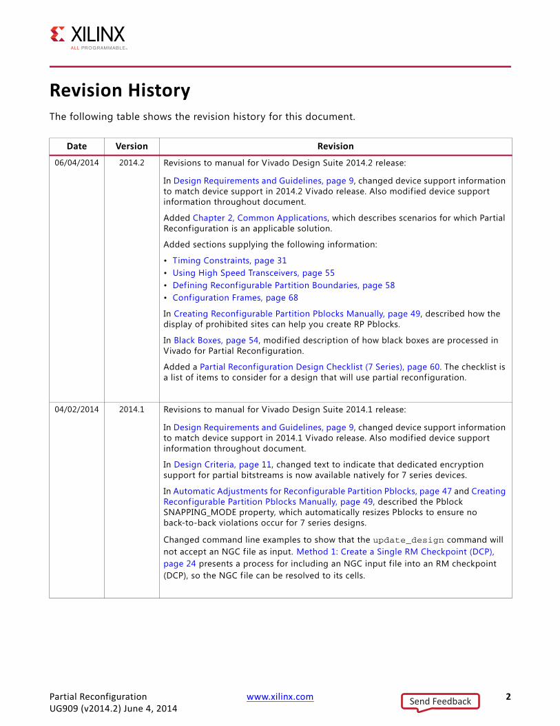
Revision HistoryThe following table shows the revision history for this document.
Date Version Revision
06/04/2014 2014.2 Revisions to manual for Vivado Design Suite 2014.2 release:
In Design Requirements and Guidelines, page 9, changed device support information to match device support in 2014.2 Vivado release. Also modified device support information throughout document.
Added Chapter 2, Common Applications, which describes scenarios for which Partial Reconfiguration is an applicable solution.
Added sections supplying the following information:
• Timing Constraints, page 31• Using High Speed Transceivers, page 55• Defining Reconfigurable Partition Boundaries, page 58• Configuration Frames, page 68
In Creating Reconfigurable Partition Pblocks Manually, page 49, described how the display of prohibited sites can help you create RP Pblocks.
In Black Boxes, page 54, modified description of how black boxes are processed in Vivado for Partial Reconfiguration.
Added a Partial Reconfiguration Design Checklist (7 Series), page 60. The checklist is a list of items to consider for a design that will use partial reconfiguration.
04/02/2014 2014.1 Revisions to manual for Vivado Design Suite 2014.1 release:
In Design Requirements and Guidelines, page 9, changed device support information to match device support in 2014.1 Vivado release. Also modified device support information throughout document.
In Design Criteria, page 11, changed text to indicate that dedicated encryption support for partial bitstreams is now available natively for 7 series devices.
In Automatic Adjustments for Reconfigurable Partition Pblocks, page 47 and Creating Reconfigurable Partition Pblocks Manually, page 49, described the Pblock SNAPPING_MODE property, which automatically resizes Pblocks to ensure no back-to-back violations occur for 7 series designs.
Changed command line examples to show that the update_design command will not accept an NGC file as input. Method 1: Create a Single RM Checkpoint (DCP), page 24 presents a process for including an NGC input file into an RM checkpoint (DCP), so the NGC file can be resolved to its cells.
Send Feedback
Table of ContentsRevision History . . . . . . . . . . . . . . . . . . . . . . . . . . . . . . . . . . . . . . . . . . . . . . . . . . . . . . . . . . . . . . . . . . . . 2
Chapter 1: IntroductionOverview . . . . . . . . . . . . . . . . . . . . . . . . . . . . . . . . . . . . . . . . . . . . . . . . . . . . . . . . . . . . . . . . . . . . . . . . 5Introduction to Partial Reconfiguration . . . . . . . . . . . . . . . . . . . . . . . . . . . . . . . . . . . . . . . . . . . . . . . . 6Terminology . . . . . . . . . . . . . . . . . . . . . . . . . . . . . . . . . . . . . . . . . . . . . . . . . . . . . . . . . . . . . . . . . . . . . . 7Design Considerations . . . . . . . . . . . . . . . . . . . . . . . . . . . . . . . . . . . . . . . . . . . . . . . . . . . . . . . . . . . . . . 9
Chapter 2: Common ApplicationsNetworked Multiport Interface . . . . . . . . . . . . . . . . . . . . . . . . . . . . . . . . . . . . . . . . . . . . . . . . . . . . . 13Configuration by Means of Standard Bus Interface. . . . . . . . . . . . . . . . . . . . . . . . . . . . . . . . . . . . . . 15Dynamically Reconfigurable Packet Processor . . . . . . . . . . . . . . . . . . . . . . . . . . . . . . . . . . . . . . . . . 17Asymmetric Key Encryption . . . . . . . . . . . . . . . . . . . . . . . . . . . . . . . . . . . . . . . . . . . . . . . . . . . . . . . . 18Summary. . . . . . . . . . . . . . . . . . . . . . . . . . . . . . . . . . . . . . . . . . . . . . . . . . . . . . . . . . . . . . . . . . . . . . . . 19
Chapter 3: Vivado Software FlowSoftware Flow Overview . . . . . . . . . . . . . . . . . . . . . . . . . . . . . . . . . . . . . . . . . . . . . . . . . . . . . . . . . . . 20Partial Reconfiguration Commands . . . . . . . . . . . . . . . . . . . . . . . . . . . . . . . . . . . . . . . . . . . . . . . . . . 21Partial Reconfiguration Constraints and Properties . . . . . . . . . . . . . . . . . . . . . . . . . . . . . . . . . . . . . 26Software Flow . . . . . . . . . . . . . . . . . . . . . . . . . . . . . . . . . . . . . . . . . . . . . . . . . . . . . . . . . . . . . . . . . . . 35Tcl Scripts . . . . . . . . . . . . . . . . . . . . . . . . . . . . . . . . . . . . . . . . . . . . . . . . . . . . . . . . . . . . . . . . . . . . . . . 39
Chapter 4: Design Considerations and GuidelinesIntroduction . . . . . . . . . . . . . . . . . . . . . . . . . . . . . . . . . . . . . . . . . . . . . . . . . . . . . . . . . . . . . . . . . . . . . 40Design Hierarchy . . . . . . . . . . . . . . . . . . . . . . . . . . . . . . . . . . . . . . . . . . . . . . . . . . . . . . . . . . . . . . . . . 40Global Clocking Rules. . . . . . . . . . . . . . . . . . . . . . . . . . . . . . . . . . . . . . . . . . . . . . . . . . . . . . . . . . . . . . 44Partition Pin Placement. . . . . . . . . . . . . . . . . . . . . . . . . . . . . . . . . . . . . . . . . . . . . . . . . . . . . . . . . . . . 45Active Low Resets and Clock Enables . . . . . . . . . . . . . . . . . . . . . . . . . . . . . . . . . . . . . . . . . . . . . . . . . 46Decoupling Functionality. . . . . . . . . . . . . . . . . . . . . . . . . . . . . . . . . . . . . . . . . . . . . . . . . . . . . . . . . . . 46Reconfigurable Partition Pblock Sizes and Shapes . . . . . . . . . . . . . . . . . . . . . . . . . . . . . . . . . . . . . . 47Black Boxes. . . . . . . . . . . . . . . . . . . . . . . . . . . . . . . . . . . . . . . . . . . . . . . . . . . . . . . . . . . . . . . . . . . . . . 54Using High Speed Transceivers . . . . . . . . . . . . . . . . . . . . . . . . . . . . . . . . . . . . . . . . . . . . . . . . . . . . . . 55Effective Approaches for Implementation . . . . . . . . . . . . . . . . . . . . . . . . . . . . . . . . . . . . . . . . . . . . . 56
Partial Reconfiguration www.xilinx.com 3UG909 (v2014.2) June 4, 2014
Send Feedback
Defining Reconfigurable Partition Boundaries . . . . . . . . . . . . . . . . . . . . . . . . . . . . . . . . . . . . . . . . . 58Design Revision Checks . . . . . . . . . . . . . . . . . . . . . . . . . . . . . . . . . . . . . . . . . . . . . . . . . . . . . . . . . . . . 59Simulation and Verification. . . . . . . . . . . . . . . . . . . . . . . . . . . . . . . . . . . . . . . . . . . . . . . . . . . . . . . . . 59Partial Reconfiguration Design Checklist (7 Series) . . . . . . . . . . . . . . . . . . . . . . . . . . . . . . . . . . . . . . 60
Chapter 5: Configuring the FPGA DeviceConfiguration Overview . . . . . . . . . . . . . . . . . . . . . . . . . . . . . . . . . . . . . . . . . . . . . . . . . . . . . . . . . . . 63Configuration Modes . . . . . . . . . . . . . . . . . . . . . . . . . . . . . . . . . . . . . . . . . . . . . . . . . . . . . . . . . . . . . . 64Downloading a Full Bit File . . . . . . . . . . . . . . . . . . . . . . . . . . . . . . . . . . . . . . . . . . . . . . . . . . . . . . . . . 65Downloading a Partial Bit File . . . . . . . . . . . . . . . . . . . . . . . . . . . . . . . . . . . . . . . . . . . . . . . . . . . . . . . 66System Design for Configuring an FPGA Device. . . . . . . . . . . . . . . . . . . . . . . . . . . . . . . . . . . . . . . . . 67Partial Bitstream CRC Checking. . . . . . . . . . . . . . . . . . . . . . . . . . . . . . . . . . . . . . . . . . . . . . . . . . . . . . 68Configuration Frames . . . . . . . . . . . . . . . . . . . . . . . . . . . . . . . . . . . . . . . . . . . . . . . . . . . . . . . . . . . . . 68Configuration Time . . . . . . . . . . . . . . . . . . . . . . . . . . . . . . . . . . . . . . . . . . . . . . . . . . . . . . . . . . . . . . . 69Configuration Debugging. . . . . . . . . . . . . . . . . . . . . . . . . . . . . . . . . . . . . . . . . . . . . . . . . . . . . . . . . . . 69
Chapter 6: Known Issues and LimitationsKnown Issues . . . . . . . . . . . . . . . . . . . . . . . . . . . . . . . . . . . . . . . . . . . . . . . . . . . . . . . . . . . . . . . . . . . . 73Known Limitations . . . . . . . . . . . . . . . . . . . . . . . . . . . . . . . . . . . . . . . . . . . . . . . . . . . . . . . . . . . . . . . . 74
Appendix A: Additional Resources and Legal NoticesXilinx Resources . . . . . . . . . . . . . . . . . . . . . . . . . . . . . . . . . . . . . . . . . . . . . . . . . . . . . . . . . . . . . . . . . . 75Solution Centers. . . . . . . . . . . . . . . . . . . . . . . . . . . . . . . . . . . . . . . . . . . . . . . . . . . . . . . . . . . . . . . . . . 75References . . . . . . . . . . . . . . . . . . . . . . . . . . . . . . . . . . . . . . . . . . . . . . . . . . . . . . . . . . . . . . . . . . . . . . 75Please Read: Important Legal Notices . . . . . . . . . . . . . . . . . . . . . . . . . . . . . . . . . . . . . . . . . . . . . . . . 76
Partial Reconfiguration www.xilinx.com 4UG909 (v2014.2) June 4, 2014
Send Feedback
Chapter 1
Introduction
OverviewPartial Reconfiguration allows for the dynamic change of modules within an active design. This flow requires the implementation of multiple configurations which ultimately results in full bitstreams for each configuration, and partial bitstreams for each Reconfigurable Module.
The number of configurations required varies by the number of modules that need to be implemented. However, all configurations use the same top-level, or static, placement and routing results. These static results are exported from the initial configuration, and imported by all subsequent configurations using checkpoints.
This guide:
• Is intended for designers who want to create a partially reconfigurable FPGA design.
• Assumes familiarity with FPGA design software, particularly Xilinx® Vivado® Design Suite.
• Has been written specifically for Vivado Design Suite Release 2014.2. This release supports Partial Reconfiguration for Virtex®-7, Kintex®-7, Artix®-7, and Zynq®-7000 AP SoC devices.
• Describes Partial Reconfiguration as implemented in the Vivado toolset.
VIDEO: For an overview of the Vivado Partial Reconfiguration solution in 7 series devices, see the Vivado Design Suite QuickTake Video: Partial Reconfiguration in Vivado.
Partial Reconfiguration www.xilinx.com 5UG909 (v2014.2) June 4, 2014
Send Feedback
Chapter 1: Introduction
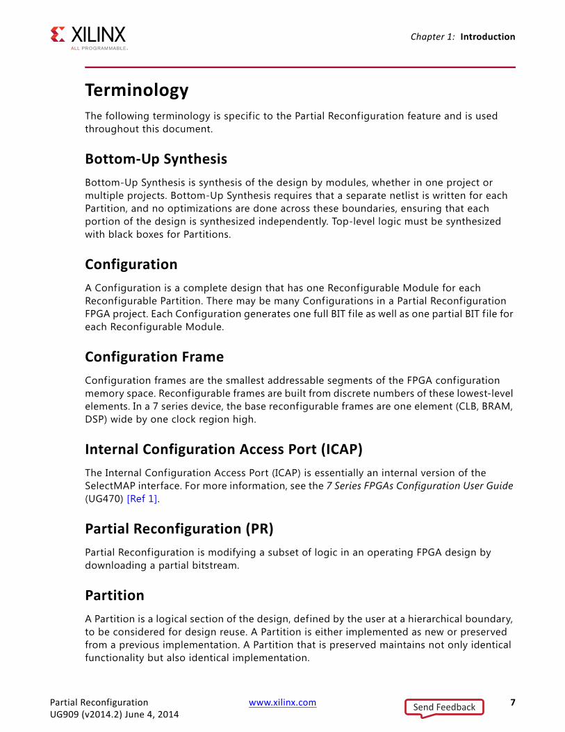
Introduction to Partial ReconfigurationFPGA technology provides the flexibility of on-site programming and re-programming without going through re-fabrication with a modified design. Partial Reconfiguration (PR) takes this flexibility one step further, allowing the modif ication of an operating FPGA design by loading a partial configuration file, usually a partial BIT f ile. After a full BIT f ile configures the FPGA, partial BIT f iles can be downloaded to modify reconfigurable regions in the FPGA without compromising the integrity of the applications running on those parts of the device that are not being reconfigured.
Figure 1-1 illustrates the premise behind Partial Reconfiguration.
As shown, the function implemented in Reconfig Block A is modified by downloading one of several partial BIT f iles, A1.bit, A2.bit, A3.bit, or A4.bit. The logic in the FPGA design is divided into two different types, reconfigurable logic and static logic. The gray area of the FPGA block represents static logic and the block portion labeled Reconfig Block "A" represents reconfigurable logic. The static logic remains functioning and is unaffected by the loading of a partial BIT f ile. The reconfigurable logic is replaced by the contents of the partial BIT f ile.
There are many reasons why the ability to time multiplex hardware dynamically on a single FPGA device is advantageous. These include:
• Reducing the size of the FPGA device required to implement a given function, with consequent reductions in cost and power consumption
• Providing flexibility in the choices of algorithms or protocols available to an application
• Enabling new techniques in design security
• Improving FPGA fault tolerance
• Accelerating configurable computing
In addition to reducing size, weight, power and cost, Partial Reconfiguration enables new types of FPGA designs that are impossible to implement without it.
X-Ref Target - Figure 1-1
Figure 1-1: Basic Premise of Partial Reconfiguration
FPGA
ReconfigBlock “A”
A4.bitA3.bit
A2.bitA1.bit
X12001
Partial Reconfiguration www.xilinx.com 6UG909 (v2014.2) June 4, 2014
Send Feedback
Chapter 1: Introduction
TerminologyThe following terminology is specific to the Partial Reconfiguration feature and is used throughout this document.
Bottom-Up SynthesisBottom-Up Synthesis is synthesis of the design by modules, whether in one project or multiple projects. Bottom-Up Synthesis requires that a separate netlist is written for each Partition, and no optimizations are done across these boundaries, ensuring that each portion of the design is synthesized independently. Top-level logic must be synthesized with black boxes for Partitions.
ConfigurationA Configuration is a complete design that has one Reconfigurable Module for each Reconfigurable Partition. There may be many Configurations in a Partial Reconfiguration FPGA project. Each Configuration generates one full BIT f ile as well as one partial BIT f ile for each Reconfigurable Module.
Configuration FrameConfiguration frames are the smallest addressable segments of the FPGA configuration memory space. Reconfigurable frames are built from discrete numbers of these lowest-level elements. In a 7 series device, the base reconfigurable frames are one element (CLB, BRAM, DSP) wide by one clock region high.
Internal Configuration Access Port (ICAP)The Internal Configuration Access Port (ICAP) is essentially an internal version of the SelectMAP interface. For more information, see the 7 Series FPGAs Configuration User Guide (UG470) [Ref 1].
Partial Reconfiguration (PR)Partial Reconfiguration is modifying a subset of logic in an operating FPGA design by downloading a partial bitstream.
PartitionA Partition is a logical section of the design, defined by the user at a hierarchical boundary, to be considered for design reuse. A Partition is either implemented as new or preserved from a previous implementation. A Partition that is preserved maintains not only identical functionality but also identical implementation.
Partial Reconfiguration www.xilinx.com 7UG909 (v2014.2) June 4, 2014
Send Feedback
Chapter 1: Introduction
Partition PinPartition pins are the logical and physical connection between static logic and reconfigurable logic. Partition pins are automatically created for all Reconfigurable Partition ports.
Processor Configuration Access Port (PCAP)The Processor Configuration Access Port (PCAP) is similar to the Internal Configuration Access Port (ICAP) and is the primary port used for configuring a Zynq-7000 device. For more information, see the Zynq-7000 All Programmable Technical Reference Manual (UG585) [Ref 2].
Reconfigurable FrameReconfigurable frames (in all references other than "configuration frames" in this guide) represent the smallest reconfigurable region within an FPGA device. Bitstream sizes of reconfigurable frames vary depending on the types of logic contained within the frame.
Reconfigurable LogicReconfigurable Logic is any logical element that is part of a Reconfigurable Module. These logical elements are modified when a partial BIT f ile is loaded. Many types of logical components may be reconfigured such as LUTs, flip-flops, BRAM, and DSP blocks.
Reconfigurable Module (RM)A Reconfigurable Module (RM) is the netlist or HDL description that is implemented within a Reconfigurable Partition. Multiple Reconfigurable Modules will exist for a Reconfigurable Partition.
Reconfigurable Partition (RP)Reconfigurable Partition (RP) is an attribute set on an instantiation that defines the instance as reconfigurable. The Reconfigurable Partition is the level of hierarchy within which different Reconfigurable Modules will be implemented. Tcl commands such as opt_design, place_design and route_design detect the HD.RECONFIGURABLE property on the instance and process it correctly.
Static LogicStatic Logic is any logical element that is not part of a Reconfigurable Partition. The logical element is never partially reconfigured and is always active when Reconfigurable Partitions are being reconfigured. Static Logic is also known as Top-level Logic.
Partial Reconfiguration www.xilinx.com 8UG909 (v2014.2) June 4, 2014
Send Feedback
Chapter 1: Introduction
Static DesignThe Static Design is the part of the design that will not change during partial reconfiguration. The static design includes the top level and all modules not defined as reconfigurable. The Static Design is built with Static Logic and Static Routing.
Design ConsiderationsPartial Reconfiguration (PR) is an expert flow within the Vivado Design Suite. Prospective customers must understand the following requirements and expectations before embarking on a PR project.
Design Requirements and Guidelines• Partial Reconfiguration requires the use of Vivado 2013.3 or newer.
° Partial Reconfiguration is supported in the ISE Design Suite as well. The ISE Design Suite should only be used for Partial Reconfiguration support of Virtex-6, Virtex-5 and Virtex-4 devices. See the Partial Reconfiguration User Guide (UG702) [Ref 3] for more information.
• Device support: All Artix-7, Kintex-7, Virtex-7, and Zynq AP SoC devices.
° New devices added in the 2014.2 Vivado Design Suite release:
- Artix-7: 7A50T and 7A35T
° UltraScale™ devices are not yet supported.
• PR is supported via Tcl or command line only; there is no project support at this time.
• Floorplanning is required to define reconfigurable regions, per element type.
° For greatest eff iciency, and to use the RESET_AFTER_RECONFIG feature, vertically align to frame/clock region boundaries.
° Horizontal alignment rules also apply. See Create a Floorplan for the Reconfigurable Region in Chapter 3 for more information.
• Bottom-up synthesis (to create multiple netlist f iles) and management of Reconfigurable Module netlist f iles is the responsibility of the user.
° Any synthesis tool may be used. Disable I/O insertion to create Reconfigurable Module netlists.
° Vivado Synthesis uses the out-of-context Module Analysis flow for Reconfigurable Module synthesis.
• Standard timing constraints are supported, and additional timing budgeting capabilities are available if needed.
Partial Reconfiguration www.xilinx.com 9UG909 (v2014.2) June 4, 2014
Send Feedback
Chapter 1: Introduction
• A unique set of Design Rule Checks (DRCs) has been established to guide users on a successful path to design completion.
• A PR design must consider the initiation of Partial Reconfiguration as well as the delivery of partial BIT f iles, either within the FPGA or as part of the system design.
• A Reconfigurable Partition must contain a super set of all pins to be used by the varying Reconfigurable Modules implemented for the partition. It is expected that this will lead to unused inputs or outputs for some modules, and is designed into the flexibility of the PR solution. The unused inputs will be left dangling inside of the module; drive outputs to a constant if this is an issue for your design.
• Black boxes are supported for bitstream generation. See Black Boxes in Chapter 4 for details about how to tie off ports with constant values.
Design PerformancePerformance metrics will vary from design to design, and the best results will be seen when if you follow the Hierarchical Design techniques documented in the Hierarchical Design Methodology Guide (UG748) [Ref 4], and in Repeatable Results with Design Preservation (WP362) [Ref 5]. These documents were created for the ISE Design Suite, but the methodologies contained therein still apply for the Vivado Design Suite. Additional design recommendations can be found in the UltraFast Design Methodology Guide for the Vivado Design Suite (UG949) [Ref 6].
However, the additional restrictions that are required for silicon isolation are expected to have an impact on most designs. The application of Partial Reconfiguration rules, such as routing containment, exclusive placement, and no optimization across reconfigurable module boundaries, will mean that the overall density and performance will be lower for a PR design than for the equivalent flat design. The overall design performance for PR designs will vary from design to design based on factors such as the number of reconfigurable partitions, the number of interface pins to these partitions, and the size and shape of Pblocks.
Partial Reconfiguration www.xilinx.com 10UG909 (v2014.2) June 4, 2014
Send Feedback

Chapter 1: Introduction
Design Criteria• Some component types can be reconfigured and some cannot.
° Reconfigurable resources include CLB, BRAM, and DSP component types as well as routing resources.
° Clocks and Clock modifying logic cannot be reconfigured, and therefore must reside in the static region.
- Includes BUFG, BUFR, MMCM, PLL, and similar components
° The following components cannot be reconfigured, and therefore must reside in the static region:
- I/O and I/O related components (ISERDES, OSERDES, IDELAYCTRL, etc.)
- Serial transceivers (MGTs) and related components
- Individual architecture feature components (such as BSCAN, STARTUP, XADC, etc.) must remain in the static region of the design
• Global clocking resources to Reconfigurable Partitions are limited, depending on the device and on the clock regions occupied by these Reconfigurable Partitions.
• IP restrictions may occur due to components used to implement the IP. Examples include:
° Vivado Debug Hub (BSCAN and BUFG)
° IP modules with embedded global buffers or I/O
° MIG controller (MMCM)
• Reconfigurable Modules must be initialized to ensure a predictable starting condition after reconfiguration. You can do this manually with a local reset, or via dedicated GSR events by selecting the RESET_AFTER_RECONFIG feature.
• Decoupling logic is highly recommended to disconnect the reconfigurable region from the static portion of the design during the act of Partial Reconfiguration.
° Clock and other inputs to Reconfigurable Modules can be decoupled to prevent spurious writes to memories during reconfiguration. This should be considered if RESET_AFTER_RECONFIG is not used.
• A reconfigurable partition must be flooorplanned, so the module must be a block that can be contained by a Pblock and meet timing. If the module is complete, it is recommended to run this design through a non-PR flow to get an initial evaluation of placement, routing, and timing results. If the design has issues in a non-PR flow, these should be resolved before moving on to the PR flow.
Partial Reconfiguration www.xilinx.com 11UG909 (v2014.2) June 4, 2014
Send Feedback
Chapter 1: Introduction
• Each module pin on an RP will have a partition pin. This is a routing point that connects static logic to the RP. If a design has too many partition pins for the number of available routing resources, routing congestion can occur. Consider the number of external pins on the RP, and develop a module that has a minimum required set of pins.
• Virtex-7 SSI devices (7V2000T, 7VX1140T, 7VH870T, 7VH580T) have two fundamental requirements. These requirements are:
° Reconfigurable regions must be fully contained within a single SLR. This ensures that the global reset events are properly synchronized across all elements in the Reconfigurable Module, and that all Super Long Lines (SLL) are contained within the static portion of the design. SLL are not partially reconfigurable.
° If ICAP is used for partial bitstream delivery, it must be one located on the Master SLR, which is SLR1 for these devices. Apply a location constraint on the ICAP to the ICAP_X0Y2 or ICAP_X0Y3 locations only. The bitstream format is such that the standard daisy chain through the four SLRs is maintained. Do not use an ICAP on any of the other SLRs, even if the reconfigurable region is located there.
• Dedicated encryption support for partial bitstreams is available natively for 7 series devices.
• 7 series devices can utilize a per-frame CRC checking mechanism, enabled via write_bitstream, to ensure each frame is valid before loading.
Note: This feature will be implemented in a future Vivado release.
Partial Reconfiguration is a powerful capability within Xilinx FPGAs, and understanding the capabilities of the silicon and software is instrumental to success with this technology. While trade-offs must be recognized and considered during the development process, the overall result will be a more flexible implementation of your FPGA design.
Partial Reconfiguration www.xilinx.com 12UG909 (v2014.2) June 4, 2014
Send Feedback
Chapter 2
Common ApplicationsThe basic premise of Partial Reconfiguration is that the FPGA hardware resources can be time-multiplexed similar to the ability of a microprocessor to switch tasks. Because the FPGA device is switching tasks in hardware, it has the benefit of both flexibility of a software implementation and the performance of a hardware implementation. A number of different scenarios are presented here to illustrate the power of this technology.
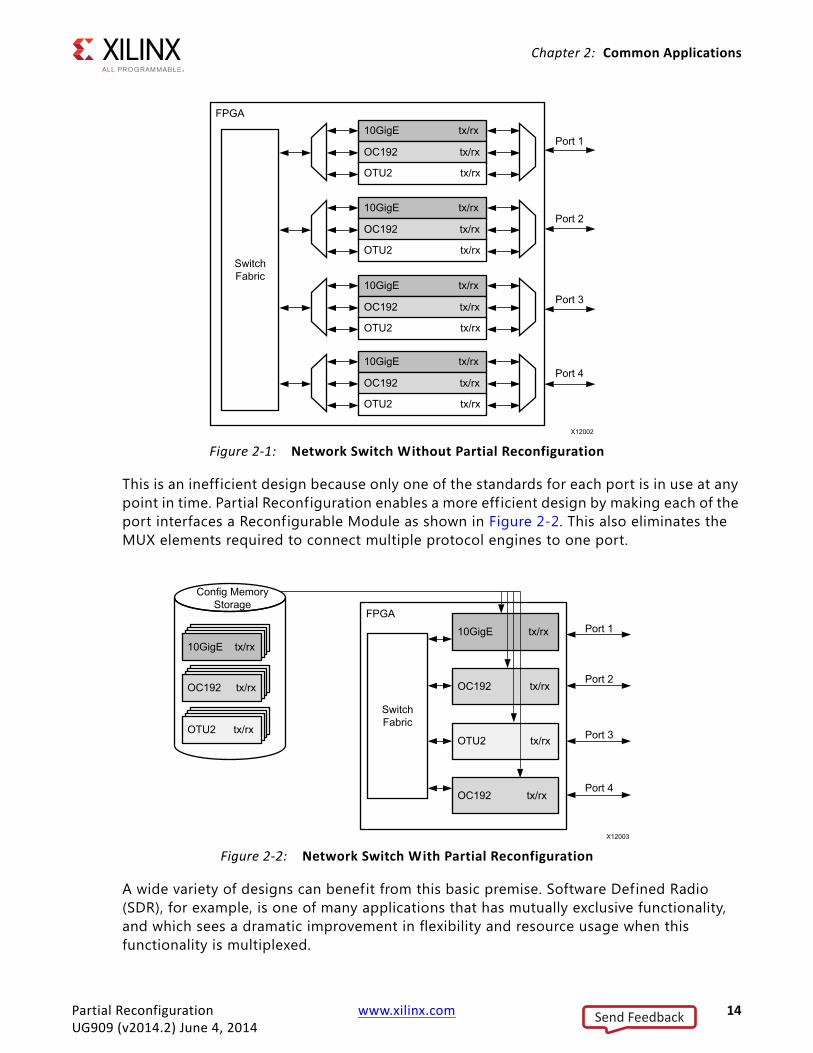
Networked Multiport InterfacePartial Reconfiguration optimizes traditional FPGA applications by reducing size, weight, power, and cost. Time-independent functions can be identif ied, isolated, and implemented as Reconfigurable Modules and swapped in and out of a single device as needed. A typical example is a 40G OTN muxponder application. The ports of the client side of the muxponder may support multiple interface protocols; however, it is not possible for the system to predict which protocol will be used before the FPGA device is configured. To ensure that the FPGA device does not have to be reconfigured and thus disable all ports, every possible interface protocol is implemented for every port, as illustrated in Figure 2-1.
Partial Reconfiguration www.xilinx.com 13UG909 (v2014.2) June 4, 2014
Send Feedback
Chapter 2: Common Applications
This is an inefficient design because only one of the standards for each port is in use at any point in time. Partial Reconfiguration enables a more eff icient design by making each of the port interfaces a Reconfigurable Module as shown in Figure 2-2. This also eliminates the MUX elements required to connect multiple protocol engines to one port.
A wide variety of designs can benefit from this basic premise. Software Defined Radio (SDR), for example, is one of many applications that has mutually exclusive functionality, and which sees a dramatic improvement in flexibility and resource usage when this functionality is multiplexed.
X-Ref Target - Figure 2-1
Figure 2-1: Network Switch Without Partial Reconfiguration
X-Ref Target - Figure 2-2
Figure 2-2: Network Switch With Partial Reconfiguration
Partial Reconfiguration www.xilinx.com 14UG909 (v2014.2) June 4, 2014
Send Feedback
Chapter 2: Common Applications
There are additional advantages with a partially reconfigurable design other than eff iciency. In the Figure 2-2 example, a new protocol can be supported at any time without affecting the static logic, the switch fabric in this example. When a new standard is loaded for any port, the other existing ports are not affected in any way. Additional standards can be created and added to the configuration memory library without requiring a complete redesign. This allows greater flexibility and reliability with less down time for the switch fabric and the ports. A debug module could be created so that if a port was experiencing errors, an unused port could be loaded with analysis/correction logic to handle the problem real-time.
In the Figure 2-2 example, a unique partial BIT f ile must be generated for each unique physical location that could be targeted by each protocol. Partial BIT f iles are associated with an explicit region on the device. In this example, sixteen unique partial BIT f iles to accommodate four protocols for four locations.
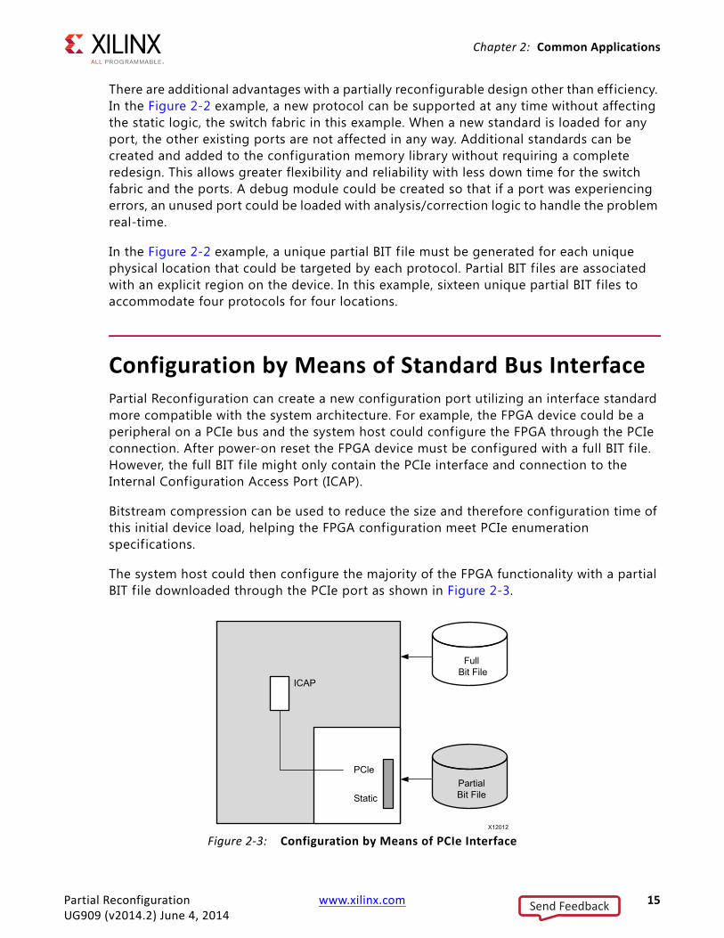
Configuration by Means of Standard Bus InterfacePartial Reconfiguration can create a new configuration port utilizing an interface standard more compatible with the system architecture. For example, the FPGA device could be a peripheral on a PCIe bus and the system host could configure the FPGA through the PCIe connection. After power-on reset the FPGA device must be configured with a full BIT f ile. However, the full BIT f ile might only contain the PCIe interface and connection to the Internal Configuration Access Port (ICAP).
Bitstream compression can be used to reduce the size and therefore configuration time of this initial device load, helping the FPGA configuration meet PCIe enumeration specifications.
The system host could then configure the majority of the FPGA functionality with a partial BIT f ile downloaded through the PCIe port as shown in Figure 2-3.
X-Ref Target - Figure 2-3
Figure 2-3: Configuration by Means of PCIe Interface
Partial Reconfiguration www.xilinx.com 15UG909 (v2014.2) June 4, 2014
Send Feedback
Chapter 2: Common Applications
The PCIe standard requires the peripheral (the FPGA device in this case) to acknowledge any requests even if it cannot service the request. Reconfiguring the entire FPGA device would violate this requirement. Because the PCIe interface is part of the static logic, it is always active during the Partial Reconfiguration process thus ensuring that the FPGA device can respond to PCIe commands even during reconfiguration.
Tandem Configuration is a related solution that at f irst glance appears to be the same as is shown here. However, the solution using Partial Reconfiguration differs from Tandem Configuration on 7 series devices in two regards:
• First, the configuration process with PR is a full device configuration, made smaller and faster via compression, followed by a partial bitstream that overwrites the black box region to complete the overall configuration. Tandem Configuration is a two-stage configuration where each configuration frame is programmed exactly once.
• Second, Tandem Configuration for 7 series devices does not permit dynamic reconfiguration of the user application. Using Partial Reconfiguration, the dynamic region can be reloaded with different user applications or f ield updates.
Tandem Configuration is designed to be a specif ic solution for a specific goal: fast configuration of a PCIe endpoint to meet enumeration requirements. For more information, see the 7 Series FPGAs Integrated Block for PCI Express Product Guide (PG054) [Ref 7] and the Virtex-7 FPGA Gen3 PCIe Integrated Block for PCI Express Product Guide (PG023) [Ref 8].
Partial Reconfiguration www.xilinx.com 16UG909 (v2014.2) June 4, 2014
Send Feedback
Chapter 2: Common Applications
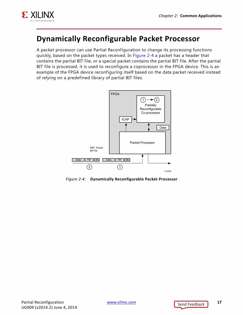
Dynamically Reconfigurable Packet ProcessorA packet processor can use Partial Reconfiguration to change its processing functions quickly, based on the packet types received. In Figure 2-4 a packet has a header that contains the partial BIT f ile, or a special packet contains the partial BIT f ile. After the partial BIT f ile is processed, it is used to reconfigure a coprocessor in the FPGA device. This is an example of the FPGA device reconfiguring itself based on the data packet received instead of relying on a predefined library of partial BIT f iles.
X-Ref Target - Figure 2-4
Figure 2-4: Dynamically Reconfigurable Packet Processor
Partial Reconfiguration www.xilinx.com 17UG909 (v2014.2) June 4, 2014
Send Feedback
Chapter 2: Common Applications
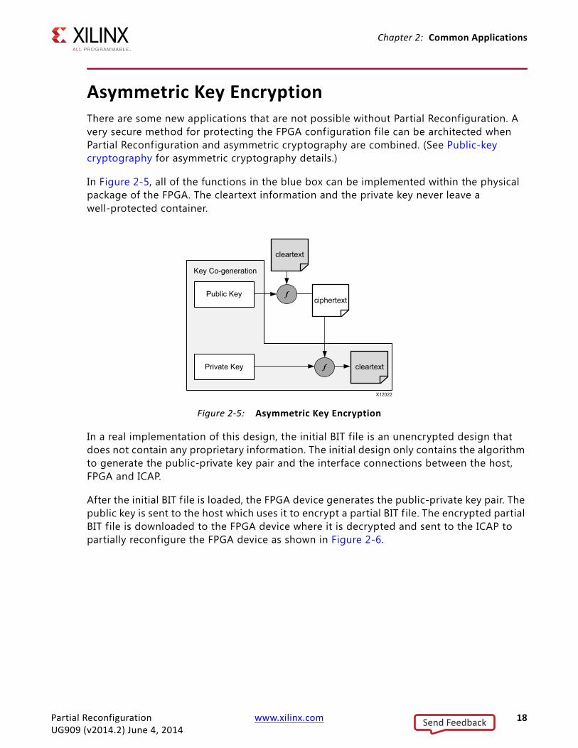
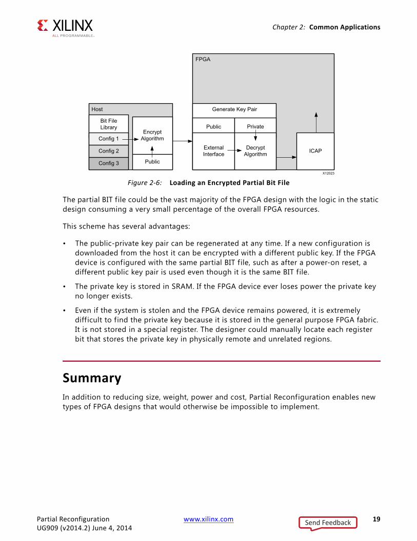
Asymmetric Key EncryptionThere are some new applications that are not possible without Partial Reconfiguration. A very secure method for protecting the FPGA configuration file can be architected when Partial Reconfiguration and asymmetric cryptography are combined. (See Public-key cryptography for asymmetric cryptography details.)
In Figure 2-5, all of the functions in the blue box can be implemented within the physical package of the FPGA. The cleartext information and the private key never leave a well-protected container.
In a real implementation of this design, the initial BIT f ile is an unencrypted design that does not contain any proprietary information. The initial design only contains the algorithm to generate the public-private key pair and the interface connections between the host, FPGA and ICAP.
After the initial BIT f ile is loaded, the FPGA device generates the public-private key pair. The public key is sent to the host which uses it to encrypt a partial BIT f ile. The encrypted partial BIT f ile is downloaded to the FPGA device where it is decrypted and sent to the ICAP to partially reconfigure the FPGA device as shown in Figure 2-6.
X-Ref Target - Figure 2-5
Figure 2-5: Asymmetric Key Encryption
Partial Reconfiguration www.xilinx.com 18UG909 (v2014.2) June 4, 2014
Send Feedback
Chapter 2: Common Applications
The partial BIT f ile could be the vast majority of the FPGA design with the logic in the static design consuming a very small percentage of the overall FPGA resources.
This scheme has several advantages:
• The public-private key pair can be regenerated at any time. If a new configuration is downloaded from the host it can be encrypted with a different public key. If the FPGA device is configured with the same partial BIT f ile, such as after a power-on reset, a different public key pair is used even though it is the same BIT f ile.
• The private key is stored in SRAM. If the FPGA device ever loses power the private key no longer exists.
• Even if the system is stolen and the FPGA device remains powered, it is extremely diff icult to find the private key because it is stored in the general purpose FPGA fabric. It is not stored in a special register. The designer could manually locate each register bit that stores the private key in physically remote and unrelated regions.
SummaryIn addition to reducing size, weight, power and cost, Partial Reconfiguration enables new types of FPGA designs that would otherwise be impossible to implement.
X-Ref Target - Figure 2-6
Figure 2-6: Loading an Encrypted Partial Bit File
Partial Reconfiguration www.xilinx.com 19UG909 (v2014.2) June 4, 2014
Send Feedback

Chapter 3
Vivado Software Flow
Software Flow OverviewThe Vivado® Partial Reconfiguration design flow is similar to a standard design flow, with some notable departures. The implementation software automatically manages the low-level details to meet silicon requirements. The user must provide guidance to define the design structure and floorplan. The steps for processing a PR design can be summarized as follows:
1. Synthesize the static and Reconfigurable Modules separately.
2. Create physical constraints (Pblocks) to define the reconfigurable regions.
3. Set the HD.RECONFIGURABLE property on each Reconfigurable Partition.
4. Implement a complete design (static and one Reconfigurable Module per Reconfigurable Partition) in context.
5. Save a design checkpoint for the full routed design.
6. Remove Reconfigurable Modules from this design and save a static-only design checkpoint.
7. Lock the static placement and routing.
8. Add new Reconfigurable Modules to the static design and implement this new configuration, saving a checkpoint for the full routed design.
9. Repeat Step 8 until all Reconfigurable Modules are implemented.
10. Run a verif ication utility (pr_verify) on all configurations.
11. Create bitstreams for each configuration.
Partial Reconfiguration www.xilinx.com 20UG909 (v2014.2) June 4, 2014
Send Feedback
Chapter 3: Vivado Software Flow
Partial Reconfiguration CommandsThe PR flows are currently only supported through the non-project batch/Tcl interface (no project based commands). Example scripts are provided in the Vivado Design Suite Tutorial: Partial Reconfiguration (UG947) [Ref 10], along with step by step instructions for setting up the flows. See that Tutorial for more information.
The following sections describe a few specialized commands and options needed for the PR flows. Examples of how to use these commands to run a PR flow are given. For more information on individual commands, see the Vivado Design Suite Tcl Command Reference Guide (UG835) [Ref 11].
SynthesisSynthesizing a partially reconfigurable design does not require any special commands, but does require bottom-up synthesis. There are currently no unsupported commands for synthesis, optimization, or implementation.
These synthesis tools are supported:
• XST
• Synplify
• Vivado Synthesis
IMPORTANT: Bottom-up synthesis refers to a synthesis flow in which each module has its own synthesis project. This generally involves turning off automatic I/O buffer insertion for the lower level modules.
This document only covers the Vivado Synthesis flow. For information on the other flows, refer to the XST User Guide for Virtex-6, Spartan-6, and 7 Series Devices (UG687) [Ref 12], or the Synopsys Synplify documentation.
Synthesizing the Top Level
You must have a top-level netlist with a black box for each Reconfigurable Module (RM). This requires the top-level synthesis to have module/entity declarations for the partitioned instances, but no logic – the module is empty.
The top-level synthesis will infer or instantiate I/O buffers on all top level ports; I/O logic inside of a Reconfigurable Module is not supported. For more information on controlling buffer insertion, refer to the Vivado Design Suite User Guide: Synthesis (UG901) [Ref 13].
synth_design -flatten_hierarchy rebuilt -top <top_module_name> -part <part>
Partial Reconfiguration www.xilinx.com 21UG909 (v2014.2) June 4, 2014
Send Feedback
Chapter 3: Vivado Software Flow
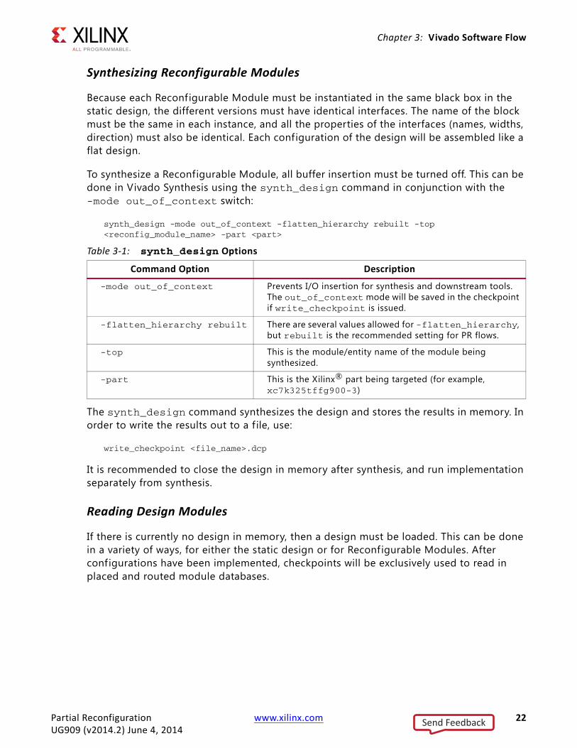
Synthesizing Reconfigurable Modules
Because each Reconfigurable Module must be instantiated in the same black box in the static design, the different versions must have identical interfaces. The name of the block must be the same in each instance, and all the properties of the interfaces (names, widths, direction) must also be identical. Each configuration of the design will be assembled like a flat design.
To synthesize a Reconfigurable Module, all buffer insertion must be turned off. This can be done in Vivado Synthesis using the synth_design command in conjunction with the -mode out_of_context switch:
synth_design -mode out_of_context -flatten_hierarchy rebuilt -top <reconfig_module_name> -part <part>
The synth_design command synthesizes the design and stores the results in memory. In order to write the results out to a f ile, use:
write_checkpoint <file_name>.dcp
It is recommended to close the design in memory after synthesis, and run implementation separately from synthesis.
Reading Design Modules
If there is currently no design in memory, then a design must be loaded. This can be done in a variety of ways, for either the static design or for Reconfigurable Modules. After configurations have been implemented, checkpoints will be exclusively used to read in placed and routed module databases.
Table 3-1: synth_design Options
Command Option Description
-mode out_of_context Prevents I/O insertion for synthesis and downstream tools. The out_of_context mode will be saved in the checkpoint if write_checkpoint is issued.
-flatten_hierarchy rebuilt There are several values allowed for -flatten_hierarchy, but rebuilt is the recommended setting for PR flows.
-top This is the module/entity name of the module being synthesized.
-part This is the Xilinx® part being targeted (for example, xc7k325tffg900-3)
Partial Reconfiguration www.xilinx.com 22UG909 (v2014.2) June 4, 2014
Send Feedback

Chapter 3: Vivado Software Flow
Method 1: Read Netlist Design
This approach should be used when modules have been synthesized by tools other than Vivado Synthesis.
read_edif <top>.edf/edn/ngc
read_edif <rp1_a>.edf/edn/ngc
read_edif <rp2_a>.edf/edn/ngc
link_design -top <top_module_name> -part <part>
Method 2: Open/Read Checkpoint
If the static (top-level) design has synthesis or implementation results stored as a checkpoint, then it can be loaded using the open_checkpoint command. This command reads in the static design checkpoint and opens it in active memory.
open_checkpoint <file>
If the checkpoint is for a reconfigurable module (i.e., not for static), then the instance name must be specified using read_checkpoint -cell. If the checkpoint is a post-implementation checkpoint, then the additional -strict option must be used as well. This option can also be used with a post-synthesis checkpoint to ensure exact port matching has been achieved. To read in a Reconfigurable Module's checkpoint, the top-level design must already be opened, and must have a black box for the specif ied cell. Then the following command can be specif ied:
read_checkpoint -cell <cellname > <file> [-strict]
Table 3-2: link_design Options
Command Option Description
-part This is the Xilinx part being targeted (for example, xc7k325tffg900-3)
-top This is the module/entity name of the module being implemented. This switch can be omitted if set_property top <top_module_name> [current_fileset] is issued prior to link_design.
Table 3-3: read_checkpoint Switches
Switch Name Description
-cell Used to specify the full hierarchical name of the Reconfigurable Module.
-strict Requires exact ports match for replacing cell, and checks that part, package, and speed grade values are identical. Should be used when restoring implementation data.
<file> Specifies the full or relative path to the checkpoint (DCP) to be read in.
Partial Reconfiguration www.xilinx.com 23UG909 (v2014.2) June 4, 2014
Send Feedback
Chapter 3: Vivado Software Flow
Method 3: Open Checkpoint/Update Design
This is useful when the synthesis results are in the form of a netlist (edf or edn), but static has already been implemented. The following example shows the commands for the second configuration in which this is true.
open_checkpoint <top>.dcp
lock_design -level routing
update_design -cells <rp1> -from_file <rp1_b>.{edf/edn}
update_design -cells <rp2> -from_file <rp2_b>.{edf/edn}
Adding Reconfigurable Modules with Multiple Netlists
If a Reconfigurable Module has sub-module netlists, it can be diff icult for the Vivado tools to process the sub-module netlists. This is because in the PR flow the RM netlists are added to a design that is already open in memory. This means the update_design -cells command must be used, which requires the cell name for every EDIF file, which can be troublesome to get.
There are two ways to make loading RM sub-module netlists easier in the Vivado Design Suite.
Method 1: Create a Single RM Checkpoint (DCP)
Create an RM checkpoint (DCP) that includes all netlists. In this case all of the EDIF (or NGC) f iles can be added using add_files, and link_design can be used to resolve the EDIF f iles to their respective cells. Here is an example of the commands used in this process:
add_files [list rm.edf ip_1.edf … ip_n.edf]
# Run if RM XDC exists
add_files rm.xdc
link_design -top <rm_module> -part <part>
write_checkpoint rm_v#.dcp
close_project
IMPORTANT: Using this methodology to combine/convert a netlist into a DCP is the recommended way to handle an RM that has one or more NGC source files as well.
Then this newly-created RM checkpoint can be used in the PR flow. In the commands below, the single read_checkpoint -cell command replaces what could be many update_design -cell commands.
add_files static.dcp
link_design -top <top> part <part>
lock_design -level routing
read_checkpoint -cell <rm_inst> rm_v#.dcp
Partial Reconfiguration www.xilinx.com 24UG909 (v2014.2) June 4, 2014
Send Feedback
Chapter 3: Vivado Software Flow
Method 2: Place the Sub-Module Netlists in the Same Directory as the RM’s Top-Level Netlist
When the top-level RM netlist is read into the PR design using update_design -cell, make sure that all sub-module netlists are in the same directory as the RM's top-level netlist. In this case the lower level netlists do not need to be specified, but they will be picked up automatically by the update_design -cells command. This is less explicit than Method 1, but requires fewer steps. In this case the commands to load the RM netlist would look like the following.
add_files static.dcp
link_design -top <top> part <part>
lock_design -level routing
update_design -cells <rm_inst> -from_file rm_v#.edf
In the last (update_design) command above, the lower level netlists will get picked up automatically if they are in the same directory as rm_v#.edf.
ImplementationSince the PR flow allows for various configurations in hardware, multiple implementation runs are required. Each implementation of a PR design is referred to as a configuration. Each module of the design (static or Reconfigurable Module) can be implemented or imported (if previously implemented). Implementation results for the static design must be consistent for each configuration, so it will be implemented in one configuration, and then imported in subsequent configurations. Additional configurations can be constructed by importing static, and implementing/importing each Reconfigurable Module.
There are no restrictions to the support of implementation commands or options for PR, but certain optimizations and sub-routines will not be done if they oppose the fundamental requirements of partial reconfiguration. The commands that may be run once the logical design is loaded (via link_design or open_checkpoint) are listed below.
# Run if all constraints are not already loaded
read_xdc
# Optional command
opt_design
place_design
# Optional command
phys_opt_design
route_design
Partial Reconfiguration www.xilinx.com 25UG909 (v2014.2) June 4, 2014
Send Feedback
Chapter 3: Vivado Software Flow
Preserving Implementation Data
In the PR flow, it is a requirement to lock down the placement and routing results of the static logic from the f irst configuration for all subsequent configurations. The static implementation of the first configuration must be saved as a checkpoint. When the checkpoint is read for subsequent configurations, the placement and routing must be locked, to ensure that the static design remains completely identical from configuration to configuration. To lock the placement and routing of an imported checkpoint (static or reconfigurable), the lock_design command is used.
lock_design -level routing [cell_name]
When locking down the static logic with the above command, the optional [cell_name] can be omitted.
lock_design -level routing
To lock the results of an imported RM, the full hierarchical name should be specified within the post-implementation checkpoint:
lock_design -level routing u0_RM_instance
For Partial Reconfiguration, the only supported preservation level is routing. Other preservation levels are available for this command, but they must only be used for other Hierarchical Design flows.
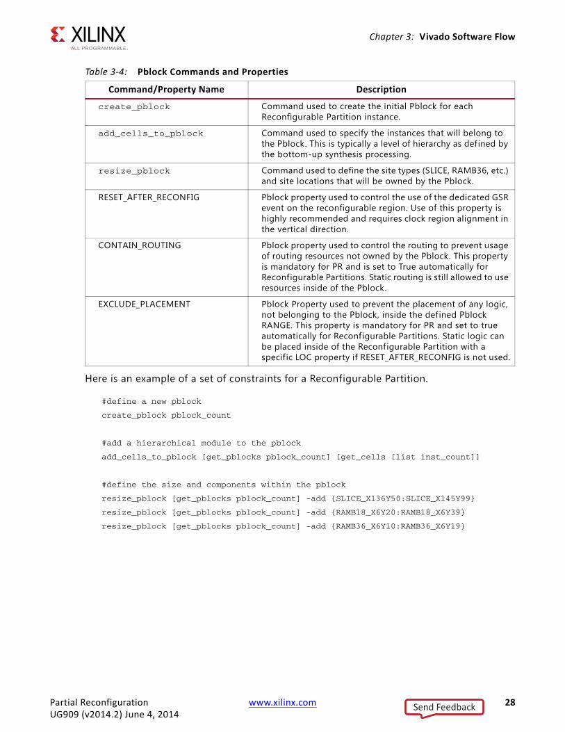
Partial Reconfiguration Constraints and PropertiesThere are a few properties and constraints unique to the Partial Reconfiguration flow. These initiate PR-specific implementation processing and apply specif ic characteristics in the partial bitstreams. The four areas for constraints and properties for partial reconfiguration are:
• Defining a module as reconfigurable - required
• Creating a floorplan for the reconfigurable region - required
• Applying reset after reconfiguration - optional, but highly recommended
• Turn on visualization scripts - optional
Partial Reconfiguration www.xilinx.com 26UG909 (v2014.2) June 4, 2014
Send Feedback

Chapter 3: Vivado Software Flow
Define a Module as ReconfigurableIn order to implement a PR design, it is required to specify each Reconfigurable Module as such. To do this you must set a property on the top level of each hierarchical cell that is going to be reconfigurable. For example, take a design where one Reconfigurable Partition named "inst_count" exists, and it has two Reconfigurable Modules, "count_up" and "count_down". The following command must be issued prior to implementation of the f irst configuration.
set_property HD.RECONFIGURABLE TRUE [get_cells inst_count]
This will initiate the Partial Reconfiguration features in the software that are required to successfully implement a PR design. The HD.RECONFIGURABLE property implies a number of underlying constraints and tasks:
• Sets DONT_TOUCH on the specif ied cell and its interface nets. This prevents optimization across the boundary of the module.
• Sets EXCLUDE_PLACEMENT on the cell's Pblock. This prevents static logic from being placed in the reconfigurable region.
• Sets CONTAIN_ROUTING on the cell's Pblock. This keeps all the routing for the Reconfigurable Module within the bounding box.
• Enables special code for DRCs, clock routing, etc.
Create a Floorplan for the Reconfigurable RegionEach Reconfigurable Partition is required to have a Pblock to define the physical resources available for the Reconfigurable Module. Because this Pblock will be set on a Reconfigurable Partition, these restrictions and requirements apply:
• The Pblock must contain only CLB/SLICE, DSP and BRAM sites. The region may overlap other site types, but these other sites must not be included in the resize_pblock commands.
• Multiple Pblock rectangles for each component type may be used to create the Reconfigurable Partition region, but for the greatest routability, they should be contiguous. Gaps to account for non-reconfigurable resources are permitted.
• If using the RESET_AFTER_RECONFIG property, the Pblock height must align to clock region boundaries. See Apply Reset After Reconfiguration for more detail.
• The width and composition of the Pblock must not split interconnect columns. See Reconfigurable Partition Pblock Sizes and Shapes in Chapter 4 for more detail.
• The Pblock must not overlap any other Pblock in the design.
• Nesting of Reconfigurable Partitions (a Reconfigurable Partition within another Reconfigurable Partition) is currently not supported.
Partial Reconfiguration www.xilinx.com 27UG909 (v2014.2) June 4, 2014
Send Feedback
Chapter 3: Vivado Software Flow
Here is an example of a set of constraints for a Reconfigurable Partition.
#define a new pblock
create_pblock pblock_count
#add a hierarchical module to the pblock
add_cells_to_pblock [get_pblocks pblock_count] [get_cells [list inst_count]]
#define the size and components within the pblock
resize_pblock [get_pblocks pblock_count] -add {SLICE_X136Y50:SLICE_X145Y99}
resize_pblock [get_pblocks pblock_count] -add {RAMB18_X6Y20:RAMB18_X6Y39}
resize_pblock [get_pblocks pblock_count] -add {RAMB36_X6Y10:RAMB36_X6Y19}
Table 3-4: Pblock Commands and Properties
Command/Property Name Description
create_pblock Command used to create the initial Pblock for each Reconfigurable Partition instance.
add_cells_to_pblock Command used to specify the instances that will belong to the Pblock. This is typically a level of hierarchy as defined by the bottom-up synthesis processing.
resize_pblock Command used to define the site types (SLICE, RAMB36, etc.) and site locations that will be owned by the Pblock.
RESET_AFTER_RECONFIG Pblock property used to control the use of the dedicated GSR event on the reconfigurable region. Use of this property is highly recommended and requires clock region alignment in the vertical direction.
CONTAIN_ROUTING Pblock property used to control the routing to prevent usage of routing resources not owned by the Pblock. This property is mandatory for PR and is set to True automatically for Reconfigurable Partitions. Static routing is still allowed to use resources inside of the Pblock.
EXCLUDE_PLACEMENT Pblock Property used to prevent the placement of any logic, not belonging to the Pblock, inside the defined Pblock RANGE. This property is mandatory for PR and set to true automatically for Reconfigurable Partitions. Static logic can be placed inside of the Reconfigurable Partition with a specific LOC property if RESET_AFTER_RECONFIG is not used.
Partial Reconfiguration www.xilinx.com 28UG909 (v2014.2) June 4, 2014
Send Feedback
Chapter 3: Vivado Software Flow
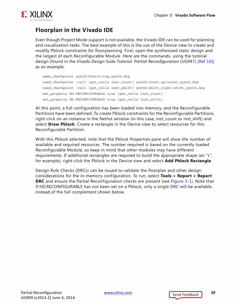
Floorplan in the Vivado IDEEven though Project Mode support is not available, the Vivado IDE can be used for planning and visualization tasks. The best example of this is the use of the Device view to create and modify Pblock constraints for floorplanning. First, open the synthesized static design and the largest of each Reconfigurable Module. Here are the commands, using the tutorial design (found in the Vivado Design Suite Tutorial: Partial Reconfiguration (UG947) [Ref 10]) as an example:
open_checkpoint synth/Static/top_synth.dcp
read_checkpoint -cell [get_cells inst_count] synth/count_up/count_synth.dcp
read_checkpoint -cell [get_cells inst_shift] synth/shift_right/shift_synth.dcp
set_property HD.RECONFIGURABLE true [get_cells inst_count]
set_property HD.RECONFIGURABLE true [get_cells inst_shift]
At this point, a full configuration has been loaded into memory, and the Reconfigurable Partitions have been defined. To create Pblock constraints for the Reconfigurable Partitions, right-click on an instance in the Netlist window (in this case, inst_count or inst_shift) and select Draw Pblock . Create a rectangle in the Device view to select resources for this Reconfigurable Partition.
With this Pblock selected, note that the Pblock Properties pane will show the number of available and required resources. The number required is based on the currently loaded Reconfigurable Module, so keep in mind that other modules may have different requirements. If additional rectangles are required to build the appropriate shape (an "L", for example), right-click the Pblock in the Device view and select Add Pblock Rectangle.
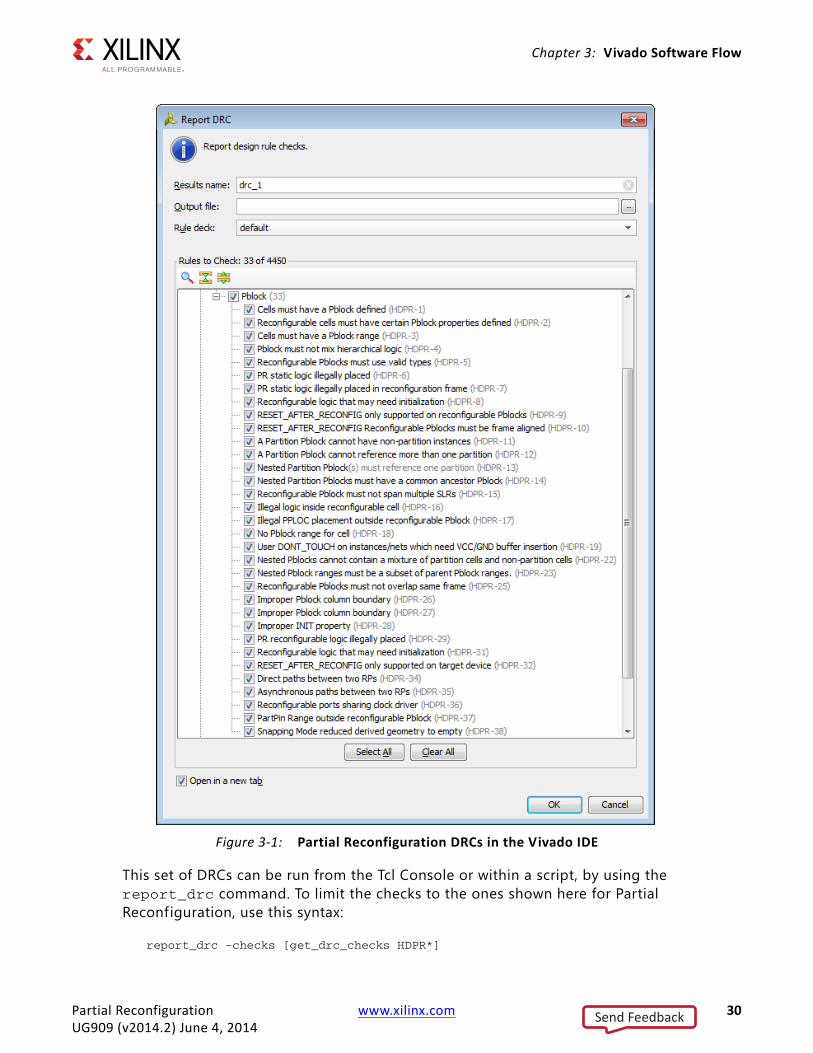
Design Rule Checks (DRCs) can be issued to validate the floorplan and other design considerations for the in-memory configuration. To run, select Tools > Report > Report DRC and ensure the Partial Reconfiguration checks are present (see Figure 3-1). Note that if HD.RECONFIGURABLE has not been set on a Pblock, only a single DRC will be available, instead of the full complement shown below.
Partial Reconfiguration www.xilinx.com 29UG909 (v2014.2) June 4, 2014
Send Feedback
Chapter 3: Vivado Software Flow
This set of DRCs can be run from the Tcl Console or within a script, by using the report_drc command. To limit the checks to the ones shown here for Partial Reconfiguration, use this syntax:
report_drc -checks [get_drc_checks HDPR*]
X-Ref Target - Figure 3-1
Figure 3-1: Partial Reconfiguration DRCs in the Vivado IDE
Partial Reconfiguration www.xilinx.com 30UG909 (v2014.2) June 4, 2014
Send Feedback
Chapter 3: Vivado Software Flow
To extend the DRCs to those checked during specific phases of design processing the -ruledeck option can be used. For example, the following command can be issued on a placed and routed design:
report_drc -ruledeck bitstream_checks
To save these floorplanning constraints, enter the following command in the Tcl Console:
write_xdc top_fplan.xdc
The Pblock constraints stored in this constraints f ile can be used directly or can be copied to another top-level design constraints f ile. This XDC file will contain all the constraints in the current design in memory, not just the constraints recently added.
CAUTION! Do NOT save the overall design from the Vivado IDE using File > Save Checkpoint or the equivalent icon. If you save the currently loaded design in this way, you will overwrite your synthesized static design checkpoint with a new version that includes Reconfigurable Modules and additional constraints.
Timing ConstraintsTiming constraints for a Partial Reconfigurable design are similar to timing constraints for a traditional flat design. The primary clocks and I/Os must be constrained with the corresponding constraints. For more information on these constraints, see the Vivado Design Suite User Guide (UG903) [Ref 14].
Once the correct constraints are applied to the design, run static timing analysis to verify the performance of the design. This verif ication must be run for each reconfigurable module in the overall static design. For more information on how to analyze the design, see the Vivado Design Suite User Guide: Design Analysis and Closure Techniques (UG906) [Ref 15].
The current constraint set does not allow the use of constraining or timing analysis for interconnect tiles at the reconfigurable module boundary. The ability to constrain and analyze for the interconnect tiles is being researched for a future release.
Partition PinsInterface points called partition pins are automatically created within the Pblock ranges defined for the Reconfigurable Partition. These virtual I/O are established within interconnect tiles as the anchor points that remain consistent from one module to the next. No physical resources such as LUTs or flip-flops are required to establish these anchor points, and no additional delay is incurred at these points.
The placer chooses locations based on source and loads and timing requirements, but these locations can be driven by the user. The following constraints may be applied to influence partition pin placement.
Partial Reconfiguration www.xilinx.com 31UG909 (v2014.2) June 4, 2014
Send Feedback
Chapter 3: Vivado Software Flow
Context Property Examples:
• set_property HD.PARTPIN_LOCS INT_R_X4Y153 [get_ports <port_name>]
• set_property HD.PARTPIN_RANGE SLICE_X4Y153:SLICE_X5Y157 [get_ports <port_name>]
Instance names for interconnect tile sites can be seen in the Device View with the Routing Resources enabled.
Apply Reset After ReconfigurationWith the Reset After Reconfiguration feature, the reconfiguring region is held in a steady state during partial reconfiguration, and then all logic in the new Reconfigurable Module is initialized to its starting values. Static routes may still freely pass unaffected through the region, and static logic (and all other PR regions) elsewhere in the device will continue to operate normally during Partial Reconfiguration. Partial Reconfiguration with this feature will behave just like the initial configuration of the FPGA, with synchronous elements being released in a known, initialized state.
IMPORTANT: Release of global signals such as GSR (Global Set Reset) and GWE (Global Write Enable) are not guaranteed to be synchronized chip-wide. If functionality within a Reconfigurable Module relies on synchronized startup of initialized sequential elements, the clock(s) driving the logic in that module or Clock Enables on these elements can be disabled during reconfiguration, then re-enabled after reconfiguration has been completed. For more details, see Answer Record 44174.
This is the RESET_AFTER_RECONFIG property syntax:
set_property RESET_AFTER_RECONFIG true [get_pblocks <reconfig_pblock_name>]
In order to apply the Reset After Reconfiguration methodology, Pblock constraints must align to reconfigurable frames. Because the GSR will affect every synchronous element
Table 3-5: Context Properties
Command/Property Name Description
HD.PARTPIN_LOCS Used to define a specif ic interconnect tile (INT) for the specified port to be routed. Overrides an HD.PARTPIN_RANGE value. Affects placement and routing of logic on both sides of the Reconfigurable Partition boundary.Do not use this property on clock ports, as this will assume local routing for the clock.Do not use this property on dedicated connections.
HD.PARTPIN_RANGE Used to define a range of component sites (SLICE, DSP, BRAM) or interconnect tiles (INT) that can be used to route the specified port(s).Do not use on clock ports, as this will assume local routing for the clock.Do not use this property on dedicated connections.
Partial Reconfiguration www.xilinx.com 32UG909 (v2014.2) June 4, 2014
Send Feedback
Chapter 3: Vivado Software Flow
within the region, exclusive use of reconfiguration frames is required; static logic is not permitted within these reconfigurable frames (static routing is permitted). Pblocks must align vertically to clock regions, since that matches the base region for a reconfigurable frame. The width of a Pblock does not matter when using RESET_AFTER_RECONFIG.
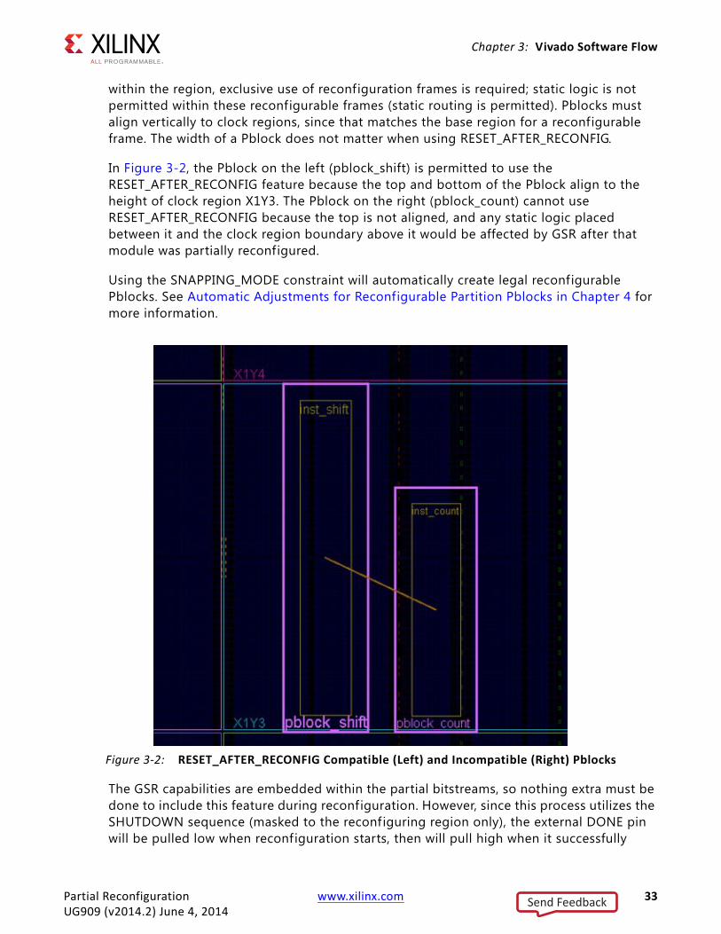
In Figure 3-2, the Pblock on the left (pblock_shift) is permitted to use the RESET_AFTER_RECONFIG feature because the top and bottom of the Pblock align to the height of clock region X1Y3. The Pblock on the right (pblock_count) cannot use RESET_AFTER_RECONFIG because the top is not aligned, and any static logic placed between it and the clock region boundary above it would be affected by GSR after that module was partially reconfigured.
Using the SNAPPING_MODE constraint will automatically create legal reconfigurable Pblocks. See Automatic Adjustments for Reconfigurable Partition Pblocks in Chapter 4 for more information.
The GSR capabilities are embedded within the partial bitstreams, so nothing extra must be done to include this feature during reconfiguration. However, since this process utilizes the SHUTDOWN sequence (masked to the reconfiguring region only), the external DONE pin will be pulled low when reconfiguration starts, then will pull high when it successfully
X-Ref Target - Figure 3-2
Figure 3-2: RESET_AFTER_RECONFIG Compatible (Left) and Incompatible (Right) Pblocks
Partial Reconfiguration www.xilinx.com 33UG909 (v2014.2) June 4, 2014
Send Feedback

Chapter 3: Vivado Software Flow
completes. This behavior must be considered when setting up the board. Using the STARTUP block's DONEO is not an option to prevent the DONE pin from changing state, since this block is disabled during shutdown. Nor can STARTUP be used for other purposes, such as generating a configuration clock for partial reconfiguration if RESET_AFTER_RECONFIG is used.
An alternative approach would be to forego this property and apply a local reset to any reconfigured logic that requires initialization to function properly. This approach does not require vertical alignment to clock region boundaries. Without GSR or a local reset, the initial starting value of a synchronous element within a reconfigured module cannot be guaranteed.
Turn On Visualization ScriptsThe configuration tiles that are part of the partial bitstreams can be visualized within the Device View in the Vivado IDE. These are identif ied via scripts that are created during implementation. To turn on script creation, set this parameter before starting implementation:
set_param HD.VISUAL true
This will generate multiple scripts placed in the hd_visual directory, which is created in the directory where the run script is launched. To use these scripts, read a routed design checkpoint into the Vivado IDE, then source one of the scripts. These design-specif ic scripts will highlight configuration tiles as defined by the user, show configuration frames used to create the partial bit f ile, or show sites excluded by the PR floorplan. Additional scripts are created for other flows, such as Module Analysis or Tandem Configuration, and are not used for PR.
Partial Reconfiguration www.xilinx.com 34UG909 (v2014.2) June 4, 2014
Send Feedback
Chapter 3: Vivado Software Flow
Software FlowThis section describes the basic flow, and gives sample commands to execute this flow.
SynthesisEach module (including Static) needs to be synthesized bottom-up so that a netlist/checkpoint exists for static and each Reconfigurable Module.
1. Synthesize the top level
read_verilog top.v (and other HDL associated with the static design, includingblack box module definitions for Reconfigurable Modules)
then:
read_xdc top_synth.xdc
synth_design -top top -part xc7k70tfbg676-2
write_checkpoint top_synth.dcp
2. Synthesize a Reconfigurable Module
read_verilog rp1_a.v
synth_design -top rp1 -part xc7k70tfbg676-2 -mode out_of_context
write_checkpoint rp1_a_synth.dcp
3. Repeat for each remaining Reconfigurable Module
read_verilog rp1_b.v
synth_design -top rp1 -part xc7k70tfbg676-2 -mode out_of_context
write_checkpoint rp1_b_synth.dcp
ImplementationCreate as many configurations as necessary to implement all Reconfigurable Modules at least once. The first configuration loads in synthesis results for top and the f irst Reconfigurable Module. You must then mark the module as being reconfigurable, then run implementation. Write out a checkpoint for the complete routed configuration, and optionally for the Reconfigurable Module so it can be reused later if desired. Finally, remove the Reconfigurable Module from the design (update_design -cell -black_box) and write out a checkpoint for the locked static design alone.
Configuration 1:
open_checkpoint top_synth.dcp
read_xdc top_impl.xdc
read_checkpoint -cell rp1 rp1_a_synth.dcp
set_property HD.RECONFIGURABLE true [get_cells rp1]
Partial Reconfiguration www.xilinx.com 35UG909 (v2014.2) June 4, 2014
Send Feedback
Chapter 3: Vivado Software Flow
opt_design
place_design
route_design
write_checkpoint config1_routed.dcp
write_checkpoint -cell rp1 rp1_a_route_design.dcp
update_design -cell rp1 -black_box
lock_design -level routing
write_checkpoint static_routed.dcp
For the second configuration, load the placed and routed checkpoint for static (if it was closed), which currently has a black box for the Reconfigurable Module. Then load in the synthesis results for the second Reconfigurable Module and implement the design. Finally write out an implementation checkpoint for the second version of the Reconfigurable Module.
Configuration 2:
open_checkpoint static_routed.dcp
read_checkpoint -cell rp1 rp1_b_synth.dcp
opt_design
place_design
route_design
write_checkpoint config2_routed.dcp
write_checkpoint -cell rp1 rp1_b_route_design.dcp
TIP: Keep each configuration in a separate folder so that all intermediate checkpoints, log and report files, bit files, and other design outputs are kept unique.
If multiple Reconfigurable Partitions exist, then other configurations may be required. Additional configurations can also be created by importing previously implemented Reconfigurable Modules to create full designs that will exist in hardware. This can be useful for creating full bitstreams with a desired combination for power-up, or for performing static timing analysis, power analysis, or simulation.
IMPORTANT: See Known Issues in Chapter 6 for a current issue with reuse of implemented Reconfigurable Module checkpoints.
ReportingEach step of the implementation flow will perform design rule checks (DRCs) unique to partial reconfiguration. Keep a close eye on the messages given by the implementation steps to ensure no critical warnings are issued. These messages will guide designers to optimize module interfaces, floorplans, and other key aspects of PR designs.
Partial Reconfiguration www.xilinx.com 36UG909 (v2014.2) June 4, 2014
Send Feedback
Chapter 3: Vivado Software Flow
Reports that can be generated do not have PR-specific sections, but useful information can be extracted nonetheless. For example, utilization information can be obtained by using the -pblocks switch for the report_utilization command. This will show the used and available resources within a given reconfigurable module. Here is an example using the design from the Vivado Design Suite Tutorial: Partial Reconfiguration (UG947) [Ref 10]:
report_utilization -pblocks [get_pblocks pblock_count]
Verifying ConfigurationsOnce all configurations have been completely placed and routed, a f inal verif ication check can be done to validate consistency between these configurations using pr_verify. This command takes in multiple routed checkpoints (DCPs) as arguments, and outputs a log of any differences found in the static implementation and Partition Pin placement between them. Placement and routing within any RMs is ignored during the comparison.
When just two configurations are to be compared, list the two routed checkpoints as <file1> and <file2>. pr_verify will load both in memory and make the comparison. When more than two configurations are to be compared, provide a "master" configuration using the -initial switch, then list the remaining configurations by using the -additional switch, listing configurations in braces ({ and }). The initial configuration is kept in memory and the remaining configurations will be compared against the initial one. Bitstreams should not be generated for any configurations if any pair of configurations do not pass the PR Verify check.
pr_verify [-full_check] [-file <arg>] [-initial <arg>] [-additional <arg>] [-quiet] [-verbose] [<file1>] [<file2>]
Here is a sample command line comparing two configurations:
pr_verify -full_check config1_routed.dcp config2_routed.dcp -file pr_verify_c1_c2.log
Table 3-6: pr_verify Options
Command Option Description
-full_check Default behavior is to report the f irst difference only; if this option is selected, pr_verify will report all differences in placement or routing.
-file Filename to output results to. Send output to console if -file is not used.
-initial Select one routed design checkpoint against which all others will be compared.
-additional Select one or more routed design checkpoints to compare against the initial one. List multiple checkpoints within braces, separated by a space, as in this example:
{config2.dcp config3.dcp config4.dcp}
-quiet Ignore command errors.
-verbose Suspend message limits during command execution.
Partial Reconfiguration www.xilinx.com 37UG909 (v2014.2) June 4, 2014
Send Feedback
Chapter 3: Vivado Software Flow
Here is a second example verifying three configurations:
pr_verify -full_check -initial config1.dcp -additional {config2.dcp config3.dcp} -file three_config.log
The scripts provided with the Vivado Design Suite Tutorial: Partial Reconfiguration (UG947) [Ref 10] have a Tcl Proc called "verify_configs" that automatically runs all existing configurations through pr_verify, and report if the DCPs are compatible or not.
Bitstream GenerationJust like a flat flow, bitstreams are created with the write_bitstream command. For each design configuration, simply issue write_bitstream to create a full standard configuration f ile plus one partial bit f ile for each Reconfigurable Module within that configuration.
It is recommended to provide the configuration name and Reconfigurable Module names in the -file option specif ied with write_bitstream. Only the base bit f ile name can be modif ied, so it is important to record which Reconfigurable Modules were selected for each configuration.
Using the design above, here is an example of reading routed checkpoints (configurations) and creating bitstreams for all implemented Reconfigurable Modules.
read_checkpoint config1_routed.dcp
write_bitstream config1
This command creates a full design bitstream called config1.bit. This bitstream should be used to program the device from power-up and includes the functionality of any Reconfigurable Modules contained within. It will also create partial bit f iles config1_pblock_rp1_partial.bit and config1_pblock_rp2_partial.bit that can be used to reconfigure these modules while the FPGA continues to operate. Repeat these steps for each configuration.
If a power-on configuration of the static design only is desired, run write_bitstream on the checkpoint that has empty Reconfigurable Partitions (after -update_design -black_box ran). This "black box configuration" can be compressed to reduce the bit f ile size and configuration time. The outputs of the RPs will be undriven, so the design should be structured to power up with the decoupling logic enabled.
TIP: Rename each partial bit file to match the Reconfigurable Module instance from which it was built to uniquely identify these modules. The current solution names partial bit files only on the configuration base name and Pblock name: <base_name>_<pblock_name>_partial.bit
Bitstream compression and other advanced features can be used.
Partial Reconfiguration www.xilinx.com 38UG909 (v2014.2) June 4, 2014
Send Feedback
Chapter 3: Vivado Software Flow
CAUTION! Do not run write_bitstream directly on Reconfigurable Module checkpoints; only use full design checkpoints. Reconfigurable module checkpoints, while they are placed and routed submodules, have no information regarding the top level design implementation, and therefore would create unsuitable partial bit files.
Tcl ScriptsScripts are provided to run this flow in the Vivado Design Suite Tutorial: Partial Reconfiguration (UG947) [Ref 10]. The details of these sample scripts are documented in the tutorial itself and in the readme.txt contained in the sample design archive.
Partial Reconfiguration www.xilinx.com 39UG909 (v2014.2) June 4, 2014
Send Feedback

Chapter 4
Design Considerations and Guidelines
IntroductionThis chapter explains design requirements that are unique to Partial Reconfiguration, and covers specif ic PR features within the Xilinx® FPGA design software tools.
To take advantage of the Partial Reconfiguration capability of Xilinx FPGA devices, you must analyze the design specif ication thoroughly, and consider the requirements, characteristics, and limitations associated with PR designs. This simplif ies both the design and debug processes, and avoids potential future risks of malfunction in the design.
Design HierarchyGood hierarchical design practices resolve many complexities and diff iculties when implementing a Partially Reconfigurable FPGA design. A clear design instance hierarchy simplif ies physical and timing constraints. Registering signals at the boundary between static and reconfigurable logic eases timing closure. Grouping logic that is packed together in the same hierarchical level is necessary.
These are all well known design practices that are often not followed in general FPGA designs. Following these design rules is not strictly required in a partially reconfigurable design, but the potential negative effects of not following them are more pronounced. The benefits of Partial Reconfiguration are great, but the extra complexity in design could be more challenging to debug, especially in hardware.
For additional information about design hierarchy, see:
• Hierarchical Design Methodology Guide (UG748) [Ref 4]
• Repeatable Results with Design Preservation (WP362) [Ref 5]
Partial Reconfiguration www.xilinx.com 40UG909 (v2014.2) June 4, 2014
Send Feedback
Chapter 4: Design Considerations and Guidelines
Design Elements Inside Reconfigurable ModulesNot all logic is permitted to be actively reconfigured. Global logic and clocking resources must be placed in the static region to not only remain operational during reconfiguration, but to benefit from the initialization sequence that occurs at the end of a full device configuration.
Logic that can be placed in a Reconfigurable Module includes:
• All logic components that are mapped to a CLB slice in the FPGA. This includes LUTs (look-up tables), FFs (flip-flops), SRLs (shift registers), RAMs, and ROMs.
• Block RAM (BRAM) and FIFO:
° RAMB18E1, RAMB36E1, BRAM_SDP_MACRO, BRAM_SINGLE_MACRO, BRAM_TDP_MACRO
° FIFO18E1, FIFO36E1, FIFO_DUALCLOCK_MACRO, FIFO_SYNC_MACRO
Note: The IN_FIFO and OUT_FIFO design elements cannot be placed in an RM. These design elements must remain in static logic.
• DSP blocks: DSP48E1
• PCIe (PCI Express) - Entered using PCIe IP
All other logic must remain in static logic, and must not be placed in an RM, including:
• Clocks and Clock Modifying Logic - Includes BUFG, BUFR, MMCM, PLL, and similar components
• I/O and I/O related components (ISERDES, OSERDES, IDELAYCTRL, etc.)
• Serial transceivers (MGTs) and related components
• Individual architecture feature components (such as BSCAN, STARTUP, XADC, etc.)
Dynamic Reconfiguration Using the DRPLogic that must remain in the static region, and therefore is not available for Partial Reconfiguration, can still be reconfigured dynamically through the Dynamic Reconfiguration Port (DRP). The DRP can be used to configure logic elements such as MMCMs, PLLs, and serial transceivers (MGTs).
Information about the DRP and dynamic reconfiguration, including how to use the DRP for specific design resources, can be found in these documents:
• 7 Series FPGAs Configuration User Guide (UG470) [Ref 1]
• 7 Series FPGAs GTX/GTH Transceivers User Guide (UG476) [Ref 16]
• MMCM and PLL Dynamic Reconfiguration (7 Series) (XAPP888) [Ref 17]
Partial Reconfiguration www.xilinx.com 41UG909 (v2014.2) June 4, 2014
Send Feedback
Chapter 4: Design Considerations and Guidelines
Packing LogicAny logic that must be packed together must be placed in the same group, whether it is static or reconfigurable. For example, if a LUT and a flip-flop are expected to be placed within the same slice, they must be within the same partition. Partition boundaries are barriers to optimization.
Design Instance HierarchyThe simplest method is to instantiate the Reconfigurable Partitions in the top-level module, but this is not required since a Reconfigurable Partition may be located in any level of hierarchy. Each Reconfigurable Partition must correspond to exactly one instance – an RP may not have more than one top. The instantiation has multiple modules with which it is associated.
Reconfigurable Partition InterfacesOne of the fundamental requirements of a partially reconfigurable design is consistency between Reconfigurable Modules. As one module is swapped for another, the connections between the static design and the Reconfigurable Module must be identical, both logically and physically. In order to achieve this consistency, optimizations across the partition boundary or of the boundary itself are prohibited.
For optimal eff iciency, all ports of a Reconfigurable Partition should be actively used on the static design side. For example, if static drivers of the Reconfigurable Partition are driven by constants (0 or 1), they will be implemented via the creation of a LUT instance and local tie-off to a constant driver and cannot be trimmed away. Likewise, unconnected outputs will remain on Reconfigurable Partition outputs, creating unnecessary waste in the overall design. These measures must be taken by the implementation tools to ensure that all Reconfigurable Modules have the same port map during design assembly.
It is strongly recommended that designers examine the interface of all Reconfigurable Partitions after synthesis to ensure that as few constants or unconnected ports as possible remain. By clearing out dead logic, resource utilization will be lower, and congestion and timing closure challenges can be made easier.
Six different cases are possible for partition interface usage:
1. Both Static and Reconfigurable Module sides have active logic. (Applies to partition inputs or outputs)
This is the optimal situation. A partition pin will be inserted.
However, if partition inputs are driven by VCC or GND, it is strongly recommended that the designer pushes these constants into the Reconfigurable Modules. This will reduce LUT usage and allow the implementation tools to optimize these constants with the RM logic.
Partial Reconfiguration www.xilinx.com 42UG909 (v2014.2) June 4, 2014
Send Feedback
Chapter 4: Design Considerations and Guidelines
2. The Static side has an active driver but the Reconfigurable Module does not have active loads. (Applies to partition inputs)
This is acceptable, since this accommodates the scenario where not every Reconfigurable Module has the same I/O requirements. A partition pin will be inserted, and the unused input ports will be left unconnected.
For example, one module may require CLK_A, while a second may require CLK_B. Clock spines will be pre-routed to the Reconfigurable Partition clock regions, but the module will only tap onto the clock source that is needed. However, if a partition input is not used by any Reconfigurable Module, it should be removed from the partition instantiation.
3. The Static side has active loads but the Reconfigurable Module does not have an active driver. (Applies to partition outputs)
This is acceptable and similar to the case above. A partition pin will be inserted, and it will be driven by ground (logic 0) within the Reconfigurable Module.
4. The Static side does not have an active driver, but the Reconfigurable Module has active loads. (Applies to partition inputs)
This will result in an error that must be resolved by modifying the partition interface.
Here is an example of an error that may be seen for this scenario:
ERROR: [Opt 31-65] LUT input is undriven either due to a missing connection from a design error, or a connection removed during opt_design.
This error message would be followed by a LUT instance that is within the Reconfigurable Module.
5. Reconfigurable Module has an active driver, but the Static side has no active loads. (Applies to partition outputs)
This will not result in an error, but is far from optimal as the RM logic will remain. No partition pin will be inserted. These partition outputs should be removed.
6. Neither Static nor Reconfigurable Module sides have driver or loads for a partition port. (Applies to partition inputs or outputs)
Nothing is inserted or used, so there is no implementation ineff iciency, but it is unnecessary in terms of the instantiation port list.
Partial Reconfiguration www.xilinx.com 43UG909 (v2014.2) June 4, 2014
Send Feedback
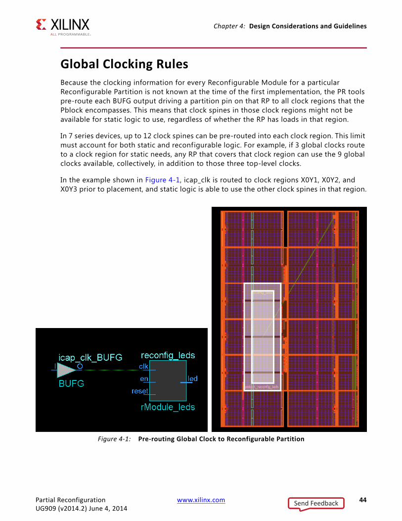
Chapter 4: Design Considerations and Guidelines
Global Clocking RulesBecause the clocking information for every Reconfigurable Module for a particular Reconfigurable Partition is not known at the time of the first implementation, the PR tools pre-route each BUFG output driving a partition pin on that RP to all clock regions that the Pblock encompasses. This means that clock spines in those clock regions might not be available for static logic to use, regardless of whether the RP has loads in that region.
In 7 series devices, up to 12 clock spines can be pre-routed into each clock region. This limit must account for both static and reconfigurable logic. For example, if 3 global clocks route to a clock region for static needs, any RP that covers that clock region can use the 9 global clocks available, collectively, in addition to those three top-level clocks.
In the example shown in Figure 4-1, icap_clk is routed to clock regions X0Y1, X0Y2, and X0Y3 prior to placement, and static logic is able to use the other clock spines in that region.
X-Ref Target - Figure 4-1
Figure 4-1: Pre-routing Global Clock to Reconfigurable Partition
Partial Reconfiguration www.xilinx.com 44UG909 (v2014.2) June 4, 2014
Send Feedback
Chapter 4: Design Considerations and Guidelines
If there are a large number of global clocks driving an RP, Xilinx recommends that area groups that encompass complete clock regions be created to ease placement and routing of static logic. Global clocks can be downgraded to regional clocks (e.g. BUFR, BUFH) for clocks with fewer loads or less demanding requirements. Shifting clocks from global to local resources will allow for more flexibility in floorplanning when the RP requires many unique clocks.
Partition Pin PlacementEach pin of an RP will have a partition pin (PartPin). By default the tools will automatically place these PartPins inside of the RP Pblock range (which is required). For many cases, this automatic placement may be suff icient for the design. However, for timing-critical interface signals or designs with high congestion, it may be necessary to help guide the placement of the PartPins. There are a few ways this can be done.
• Define user HD.PARTPIN_RANGE constraints for some or all of the pins.
set_property HD.PARTPIN_RANGE {SLICE_Xx0Yx0:SLICE_Xx1Yy1 SLICE_XxNYyN:SLICE_XxMYyM} [get_pins <rp_cell_name>/*]
By default the HD.PARTPIN_RANGE will be set to the entire Pblock range. Defining a user range allows the tools to place PartPins in the specif ied areas, improving timing and/or reducing congestion.
IMPORTANT: The automatic placement of PartPins will likely place PartPins in the corner of the Pblock rectangle. These corner locations have limited resources due to the CONTAIN_ROUTING property on the RP Pblock. If routing congestion exists around the corner of the Pblock, adding a specific HD.PARTPIN_RANGE that excludes the corner sites will help.
• By default, the tools place a maximum of 5 PartPins per interconnect (INT) tile. This can be adjusted via a param called hd.maxPPLOCSPerIntTile.
set_param hd.maxPPLOCSPerIntTile 3
Setting the value to 3 will tell the placer to put only 3 PartPins per INT tile, which will spread out the PartPin placement and reduce congestion around the RP interface.
IMPORTANT: If there are too many PartPins on the RP interface, the tools may have to violate the maximum number defined by this param. Always try to reduce the RP interface to a minimum set of pins.
Partial Reconfiguration www.xilinx.com 45UG909 (v2014.2) June 4, 2014
Send Feedback
Chapter 4: Design Considerations and Guidelines
Active Low Resets and Clock EnablesIn the Xilinx 7 series architectures there are no local inverters on control signals (resets or clock enables). The following description uses a reset as the example, but the same applies for clock enables.
If a design uses an active low reset, a LUT must be used to invert the signal. In non-PR designs that use all active low resets multiple LUTs will be inferred, but can be combined into a single LUT and pushed into the I/O elements (the LUT goes away). In non-PR designs that use a mix of high and low, the LUT inverters can be combined into one LUT that remains in the design, but that has minimal effect on routing and the timing of the reset net (output of LUT can still be put on global resources). However, for a design that uses active low resets on a partition, it is possible to have inverters inferred inside of the partition that cannot be pulled out and combined. This makes it impossible to put the reset on global resources, and can lead to poor reset timing and to routing issues if the design is already congested.
The best way to avoid this is to avoid using active low control signals. However, there are cases where this is not possible (for example, when using an IP core with an Advanced eXtensible Interface (AXI) interface). In these cases the design should assign the active- low reset to a signal at the top level, and use that new signal everywhere in the design.
As an example:
reset_n <= !reset;
Use the reset_n signal for all cases, and do not use the!reset assignments on signals or ports.
This will ensure that a LUT will be inferred only for the reset net for the whole design, and will have a minimal effect on design performance.
Decoupling FunctionalityBecause the reconfigurable logic is modified while the FPGA device is operating, the static logic connected to outputs of Reconfigurable Modules must ignore data from Reconfigurable Modules during Partial Reconfiguration. The Reconfigurable Modules will not output valid data until Partial Reconfiguration is complete and the reconfigured logic is reset. There is no way to predict or simulate the functionality of the reconfiguring module.
It is in the designer's hands to decide how the decoupling strategy is solved. A common design practice to mitigate this issue is to register all output signals (on the static side of the interface) from the Reconfigurable Module. An enable signal can be used to isolate the logic until it is completely reconfigured. Other approaches range from a simple 2 to 1 MUX on each output port, to higher level bus controller functions.
Partial Reconfiguration www.xilinx.com 46UG909 (v2014.2) June 4, 2014
Send Feedback
Chapter 4: Design Considerations and Guidelines
The static design should include the logic required for the data and interface management. It can implement mechanisms such as handshaking or disabling interfaces (which might be required for bus structures to avoid invalid transactions). It is also useful to consider the down-time performance effect of a PR module (that is, the unavailability of any shared resources included in a PR module during or after reconfiguration).
Reconfigurable Partition Pblock Sizes and ShapesAs noted in Apply Reset After Reconfiguration in Chapter 3, the height of the Reconfigurable Partition must align to clock region boundaries if RESET_AFTER_RECONFIG is to be used. Otherwise, any height may be selected for the Reconfigurable Partition.
The width of the Reconfigurable Partition must be set appropriately to make most efficient usage of interconnect and clocking resources. The left and right edges of Pblock rectangles should be placed between two resource columns (e.g. CLB-CLB, CLB-BRAM or CLB-DSP) and not between two interconnect columns (INT-INT). This allows the placer and router tools the full use of all resources for both static and reconfigurable logic. Implementation tool DRCs provide guidance if this approach is not followed.
Automatic Adjustments for Reconfigurable Partition PblocksThe Pblock SNAPPING_MODE property will automatically resize Pblocks to ensure no back-to-back violations occur for 7 series designs. When SNAPPING_MODE is set to a value of ON, it creates a new set of derived Pblock ranges that will be used for implementation. The new ranges are stored in memory, and are not written out to the XDC. Only the SNAPPING_MODE property is written out, in addition to the normal Pblock constraints.
The original Pblock rectangle(s) are not modif ied when using SNAPPING_MODE and can still be resized, moved, or extended with additional rectangles. Whenever the original Pblock rectangle is modif ied, the derived ranges are automatically recalculated. The SNAPPING_MODE property is supported in batch mode, so there is no requirement to open the current Pblock in the Vivado IDE to set SNAPPING_MODE to ON, although this option is available when performing interactive floorplanning, as shown in Figure 4-2.
Partial Reconfiguration www.xilinx.com 47UG909 (v2014.2) June 4, 2014
Send Feedback
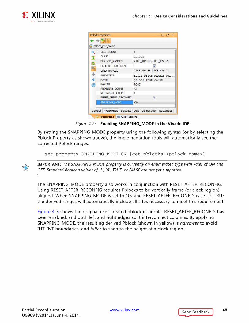
Chapter 4: Design Considerations and Guidelines
By setting the SNAPPING_MODE property using the following syntax (or by selecting the Pblock Property as shown above), the implementation tools will automatically see the corrected Pblock ranges.
set_property SNAPPING_MODE ON [get_pblocks <pblock_name>]
IMPORTANT: The SNAPPING_MODE property is currently an enumerated type with vales of ON and OFF. Standard Boolean values of '1', '0', TRUE, or FALSE are not yet supported.
The SNAPPING_MODE property also works in conjunction with RESET_AFTER_RECONFIG. Using RESET_AFTER_RECONFIG requires Pblocks to be vertically frame (or clock region) aligned. When SNAPPING_MODE is set to ON and RESET_AFTER_RECONFIG is set to TRUE, the derived ranges will automatically include all sites necessary to meet this requirement.
Figure 4-3 shows the original user-created pblock in purple. RESET_AFTER_RECONFIG has been enabled, and both left and right edges split interconnect columns. By applying SNAPPING_MODE, the resulting derived Pblock (shown in yellow) is narrower to avoid INT-INT boundaries, and taller to snap to the height of a clock region.
X-Ref Target - Figure 4-2
Figure 4-2: Enabling SNAPPING_MODE in the Vivado IDE
Partial Reconfiguration www.xilinx.com 48UG909 (v2014.2) June 4, 2014
Send Feedback

Chapter 4: Design Considerations and Guidelines
Creating Reconfigurable Partition Pblocks ManuallyIf automatic modification to the Reconfigurable Partition Pblock is not desired to fix back-to-back issues, you can create Pblock ranges manually to meet your needs. This is most useful when explicit control is needed for Pblocks that must span non-reconfigurable sites, such as configuration blocks or the center column, which contains clock buffer resources.
In Figure 4-4, note that the left and right edges are drawn between CLB columns for the Pblock highlighted in white. Visualization of the interconnect tiles as shown in this image requires that the routing resources are turned on, using this symbol in the Device View: .
X-Ref Target - Figure 4-3
Figure 4-3: Original and Derived Pblocks using SNAPPING_MODE
Partial Reconfiguration www.xilinx.com 49UG909 (v2014.2) June 4, 2014
Send Feedback
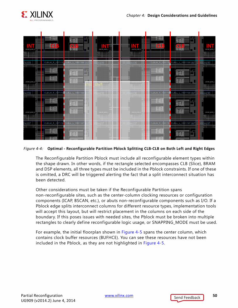
Chapter 4: Design Considerations and Guidelines
The Reconfigurable Partition Pblock must include all reconfigurable element types within the shape drawn. In other words, if the rectangle selected encompasses CLB (Slice), BRAM and DSP elements, all three types must be included in the Pblock constraints. If one of these is omitted, a DRC will be triggered alerting the fact that a split interconnect situation has been detected.
Other considerations must be taken if the Reconfigurable Partition spans non-reconfigurable sites, such as the center-column clocking resources or configuration components (ICAP, BSCAN, etc.), or abuts non-reconfigurable components such as I/O. If a Pblock edge splits interconnect columns for different resource types, implementation tools will accept this layout, but will restrict placement in the columns on each side of the boundary. If this poses issues with needed sites, the Pblock must be broken into multiple rectangles to clearly define reconfigurable logic usage, or SNAPPING_MODE must be used.
For example, the initial floorplan shown in Figure 4-5 spans the center column, which contains clock buffer resources (BUFHCE). You can see these resources have not been included in the Pblock, as they are not highlighted in Figure 4-5.
X-Ref Target - Figure 4-4
Figure 4-4: Optimal - Reconfigurable Partition Pblock Splitting CLB-CLB on Both Left and Right Edges
Partial Reconfiguration www.xilinx.com 50UG909 (v2014.2) June 4, 2014
Send Feedback
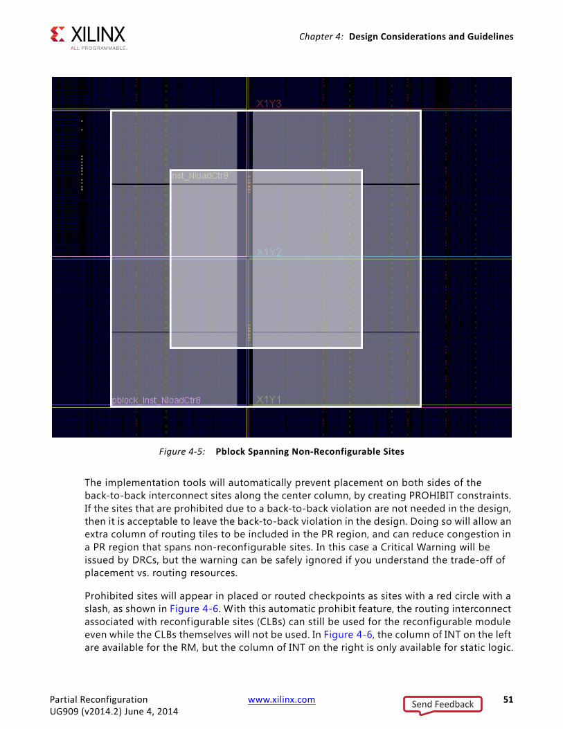
Chapter 4: Design Considerations and Guidelines
The implementation tools will automatically prevent placement on both sides of the back-to-back interconnect sites along the center column, by creating PROHIBIT constraints. If the sites that are prohibited due to a back-to-back violation are not needed in the design, then it is acceptable to leave the back-to-back violation in the design. Doing so will allow an extra column of routing tiles to be included in the PR region, and can reduce congestion in a PR region that spans non-reconfigurable sites. In this case a Critical Warning will be issued by DRCs, but the warning can be safely ignored if you understand the trade-off of placement vs. routing resources.
Prohibited sites will appear in placed or routed checkpoints as sites with a red circle with a slash, as shown in Figure 4-6. With this automatic prohibit feature, the routing interconnect associated with reconfigurable sites (CLBs) can still be used for the reconfigurable module even while the CLBs themselves will not be used. In Figure 4-6, the column of INT on the left are available for the RM, but the column of INT on the right is only available for static logic.
X-Ref Target - Figure 4-5
Figure 4-5: Pblock Spanning Non-Reconfigurable Sites
Partial Reconfiguration www.xilinx.com 51UG909 (v2014.2) June 4, 2014
Send Feedback
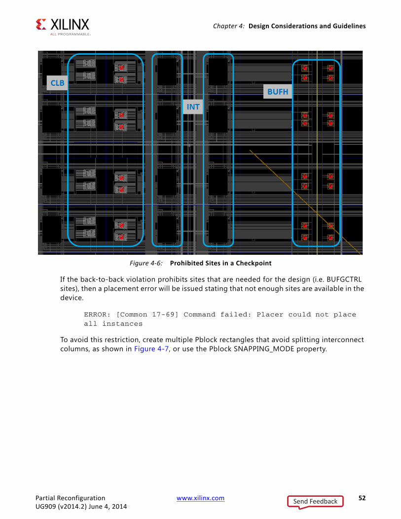
Chapter 4: Design Considerations and Guidelines
If the back-to-back violation prohibits sites that are needed for the design (i.e. BUFGCTRL sites), then a placement error will be issued stating that not enough sites are available in the device.
ERROR: [Common 17-69] Command failed: Placer could not place all instances
To avoid this restriction, create multiple Pblock rectangles that avoid splitting interconnect columns, as shown in Figure 4-7, or use the Pblock SNAPPING_MODE property.
X-Ref Target - Figure 4-6
Figure 4-6: Prohibited Sites in a Checkpoint
Partial Reconfiguration www.xilinx.com 52UG909 (v2014.2) June 4, 2014
Send Feedback
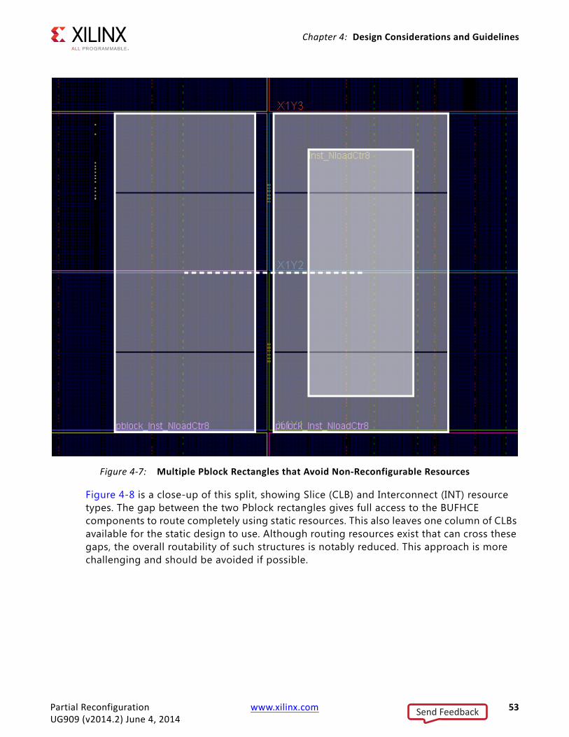
Chapter 4: Design Considerations and Guidelines
Figure 4-8 is a close-up of this split, showing Slice (CLB) and Interconnect (INT) resource types. The gap between the two Pblock rectangles gives full access to the BUFHCE components to route completely using static resources. This also leaves one column of CLBs available for the static design to use. Although routing resources exist that can cross these gaps, the overall routability of such structures is notably reduced. This approach is more challenging and should be avoided if possible.
X-Ref Target - Figure 4-7
Figure 4-7: Multiple Pblock Rectangles that Avoid Non-Reconfigurable Resources
Partial Reconfiguration www.xilinx.com 53UG909 (v2014.2) June 4, 2014
Send Feedback
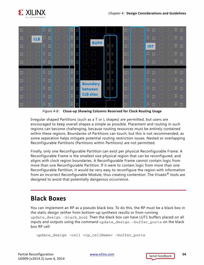
Chapter 4: Design Considerations and Guidelines
Irregular shaped Partitions (such as a T or L shapes) are permitted, but users are encouraged to keep overall shapes a simple as possible. Placement and routing in such regions can become challenging, because routing resources must be entirely contained within these regions. Boundaries of Partitions can touch, but this is not recommended, as some separation helps mitigate potential routing restriction issues. Nested or overlapping Reconfigurable Partitions (Partitions within Partitions) are not permitted.
Finally, only one Reconfigurable Partition can exist per physical Reconfigurable Frame. A Reconfigurable Frame is the smallest size physical region that can be reconfigured, and aligns with clock region boundaries. A Reconfigurable Frame cannot contain logic from more than one Reconfigurable Partition. If it were to contain logic from more than one Reconfigurable Partition, it would be very easy to reconfigure the region with information from an incorrect Reconfigurable Module, thus creating contention. The Vivado® tools are designed to avoid that potentially dangerous occurrence.
Black BoxesYou can implement an RP as a pseudo black box. To do this, the RP must be a black box in the static design (either from bottom-up synthesis results or from running update_design -black_box). Then the black box can have LUT1 buffers placed on all inputs and outputs using the command update_design -buffer_ports on the black box RP cell:
update_design -cell <rp_cellName> -buffer_ports
X-Ref Target - Figure 4-8
Figure 4-8: Close-up Showing Columns Reserved for Clock Routing Usage
Partial Reconfiguration www.xilinx.com 54UG909 (v2014.2) June 4, 2014
Send Feedback
Chapter 4: Design Considerations and Guidelines
Now you can run this design through implementation to place and route the LUT1 buffers (and static logic, if not already placed and routed).
All of the inserted LUT1 output buffers will be tied to a logic 0 (ground). If it is necessary to drive a logic 1 (VCC) from the RP outputs, this can be controlled via an RP pin property called HD.PARTPIN_TIEOFF. This property can be set at any time (all the way up to pre-write_bitstream, and it controls the LUT equation of the LUT1 buffer connected to the specified port. The default value is '0', which configures the LUT as a route-thru (output is 0). Setting this property to '1' configures the LUT as an inverter (output is 1). You may have to change the output value in some design situations.
set_property HD.PARTPIN_TIEOFF 1 [get_pins <RP_cellName>/<output_pinName>]
The pseudo black box has no user logic (just the tool inserted LUT1 buffers). The black box bitstream will contain information for these LUTs, as well as any static logic/routes that use resources inside of the RP frames. Static routes that pass through the region, including interface nets up to the partition pin nodes, exist within this region. Programming information for these signals is included in the black box programming bitstream.
Use of black boxes is an effective way to reduce the size of a full configuration BIT f ile, and therefore reduce the initial configuration time. The compression feature may also be enabled to reduce the size of BIT f iles. This option looks for repeated configuration frame structures to reduce the amount of configuration data that must be stored in the BIT f ile. The compression results in reduced configuration and reconfiguration time. When the compression option is applied to a routed PR design, all of the BIT f iles (full and partial) are created as compressed BIT f iles. To enable compression, set this property prior to running write_bitstream:
set_property BITSTREAM.GENERAL.COMPRESS TRUE [current_design]
Using High Speed TransceiversXilinx high speed transceivers (GTP, GTX, GTH, GTZ) have dedicated connections to many of their pins. These dedicated connections require that the I/O connected to these pins be handled differently than general purpose I/O. For the tools to recognize the direct connection, the transceivers and all associated I/O logic must be contained within the same Partition. This includes all the pads and buffers as well as all transceiver logic.
Partial Reconfiguration www.xilinx.com 55UG909 (v2014.2) June 4, 2014
Send Feedback
Chapter 4: Design Considerations and Guidelines
Effective Approaches for ImplementationThere are trade-offs associated with optimizing any FPGA design. Partial Reconfiguration is no different. Partitions are barriers to optimization, and reconfigurable frames require specific layout constraints. These are the additional costs to building a reconfigurable design. The additional overhead for timing and area needs vary from design to design. To minimize the impact, follow the design considerations stated in this guide.
When building Configurations of a reconfigurable design, the f irst Configuration to be chosen for implementation should be the most challenging one. Be sure that the physical region selected has adequate resources (especially elements such as BRAM and DSP48) for each Reconfigurable Module in each Reconfigurable Partition, then select the most demanding (in terms of either timing or area) RM for each RP. If all of the RMs in the subsequent Configurations are smaller or slower, it will be easier to meet their demands. Timing budgets should be established to meet the needs of all Reconfigurable Modules.
If it is not clear which reconfigurable module is the most challenging, each can be implemented in parallel in context with static, allowing static to be placed and routed for each. Examine resource utilization statistics and timing reports to see which configuration met design criteria most easily and which had the tightest tolerances, or which missed by the widest margins.
IMPORTANT: Focus attention on the configuration that is the furthest from meeting its goals, iterating on design sources, constraints, and strategies until needs are met. At some point, one configuration must be established as the golden result for the static design, and that implementation of the static logic will be used for all other configurations.
Building Up Implementation RequirementsImplementation of Partial Reconfiguration designs requires that certain fundamental rules are followed. These rules have been established to ensure that a partial bitstream can be accurately created and safely delivered to an active FPGA. As noted throughout this document, these rules include these basic premises:
• The logical and physical interface of a Reconfigurable Partition remains consistent as each Reconfigurable Module is implemented.
• The logic and routing of a Reconfigurable Module is fully contained within a physical region which will then be translated into a partial bitstream.
• The logic of the static design must be kept out of the reconfigurable region if the dedicated initialization feature is used.
These requirements necessitate specific implementation rules for optimization, placement and routing. Application of these rules may make it more diff icult to meet design goals, including timing closure. A recommended strategy is to build up this set of requirements
Partial Reconfiguration www.xilinx.com 56UG909 (v2014.2) June 4, 2014
Send Feedback

Chapter 4: Design Considerations and Guidelines
one at a time, allowing you to analyze the results at each step. Starting with the most challenging configuration and the full set of timing constraints, implement the design through place and route and examine the results, making sure you have suff icient timing slack and resources available to continue to the next step.
1. First, implement the design with no Pblocks. Use bottom-up synthesis and follow general Hierarchical Design recommendations, such as registered boundaries, to achieve a baseline result.
2. Add Pblocks for the design partitions that will later be marked reconfigurable. This floorplan can be based on the results established in the bottom-up synthesis run from Step 1. Logic from the Reconfigurable Modules must be placed in the Pblocks, but static logic may be included there as well.
While creating these Pblocks, the HD.RECONFIGURABLE property (and optionally, the RESET_AFTER_RECONFIG property) can be added temporarily in order to run PR-specific Design Rule Checks. This will ensure that the floorplan created will meet PR size and alignment requirements.
3. With the floorplan established, separate the placement of static design resources from those that will be reconfigurable by adding the EXCLUSIVE_PLACEMENT property to the Pblocks. This will keep static logic placed outside the defined Pblocks.
4. Keep the routing for Reconfigurable Modules bound within the Pblocks by applying the CONTAIN_ROUTING property to the Pblocks. With the properties from this and the previous step, the only remaining rules relate to boundary optimization procedures as well as PR-specif ic Design Rule Checks.
5. Finally, mark the Reconfigurable Partition Pblocks as HD.RECONFIGURABLE. The EXCLUSIVE_PLACEMENT and CONTAIN_ROUTING properties are now redundant and can be removed.
If design requirements are not met at any of these steps, you have to opportunity to review the design structure and constraints in light of the newly applied implementation condition.
Partial Reconfiguration www.xilinx.com 57UG909 (v2014.2) June 4, 2014
Send Feedback
Chapter 4: Design Considerations and Guidelines
Defining Reconfigurable Partition BoundariesPartial reconfiguration is done on a frame-by-frame basis. As such, when partial BIT f iles are created, they are built with a discrete number of configuration frames. The size of a partial bit f ile will depend on the number and type of frames included. You can see this size in the header of a raw bit f ile (.rbt) created by write_bitstream -rawbitfile.
Partition boundaries do not have to align to reconfigurable frame boundaries, but the most eff icient place and route results are achieved when this is done. Static logic is permitted to exist in a frame that will be reconfigured, as long as:
• It is outside the area group defined by the Pblock, and
• It does not contain dynamic elements such as Block RAM, Distributed (LUT) RAM, or SRLs.
When static logic is placed in a reconfigured frame, the exact functionality of the static logic is rewritten, and is guaranteed not to glitch.
Irregular shaped Partitions (such as a T or L shapes) are permitted but discouraged. Placement and routing in such regions can become challenging, because routing resources must be entirely contained within these regions. Boundaries of Partitions can touch, but this is not recommended, as some separation helps mitigate potential routing restriction issues as these partitions connect to the static design. Nested or overlapping Reconfigurable Partitions (Partitions within Partitions) are not permitted. Design rule checks (Tools > Report DRC) validate the Partitions and settings in a PR design.
Only one Reconfigurable Partition can exist per physical Reconfigurable Frame.
A Reconfigurable Frame is the smallest size physical region that can be reconfigured, and its height aligns with clock region or I/O bank boundaries. A Reconfigurable Frame cannot contain logic from more than one Reconfigurable Partition. If it were to contain logic from more than one Reconfigurable Partition, it would be very easy to reconfigure the region with information from an incorrect Reconfigurable Module, thus creating contention. The software tools are designed to avoid that potentially dangerous occurrence.
Partial Reconfiguration www.xilinx.com 58UG909 (v2014.2) June 4, 2014
Send Feedback
Chapter 4: Design Considerations and Guidelines
Design Revision ChecksA partial bitstream contains programming information and little else, as described in Chapter 5, Configuring the FPGA Device. While you do not need to identify the target location of the bitstream (the die location is determined by the addressing that is part of the BIT file), there are no checks in the hardware to ensure the partial bitstream is compatible with the currently operating design. Loading a partial bitstream into a static design that was not implemented with that Reconfigurable Module revision can lead to unpredictable behavior.
Xilinx suggests that you prefix a partial bitstream with a unique identif ier indicating the particular design, revision and module that follows. This identif ier can be interpreted by your configuration controller to validate that the partial bitstream is compatible with the resident design - a mismatch can be detected and the incompatible bitstream can be rejected before being loaded into configuration memory. This functionality must be part of your design, and would be similar to or in conjunction with decryption and/or CRC checks, as described in PRC/EPRC: Data Integrity and Security Controller for Partial Reconfiguration (XAPP887) [Ref 18].
A bitstream feature provides a simple mechanism for tagging a design revision. The BITSTREAM.CONFIG.USR_ACCESS property allows you to enter a revision ID directly into the bitstream. This ID is placed in the USR_ACCESS register, accessible from the FPGA fabric through a library primitive of the same name. Partial Reconfiguration designs can read this value and compare it to information in a partial bitstream to confirm the revisions of the design match. More information on this switch can be found in the Bitstream Settings Appendix in the Vivado Design Suite User Guide: Programming and Debugging (UG908) [Ref 19] and in Bitstream Identification with USR_ACCESS (XAPP497) [Ref 20].
CAUTION! Do not use the TIMESTAMP feature, since this value will not be consistent for each call to write_bitstream. Only select a consistent, explicit ID to be used for all write_bitstream runs.
Simulation and VerificationConfigurations of Partial Reconfiguration designs are complete designs in and of themselves. All standard simulation, timing analysis, and verif ication techniques are supported for PR designs. Partial reconfiguration itself cannot be simulated.
Partial Reconfiguration www.xilinx.com 59UG909 (v2014.2) June 4, 2014
Send Feedback
Chapter 4: Design Considerations and Guidelines
Partial Reconfiguration Design Checklist (7 Series)Xilinx highly encourages the following items for a 7 series FPGA design using Partial Reconfiguration:
• Recommended Clocking Networks
° Are you using Global Clock Buffers, Regional Clock Buffers, or Clock Modifying Blocks (MMCM, PLL)?
These blocks must be in static logic.
See Design Elements Inside Reconfigurable Modules, page 41 for more information, and Global Clocking Rules, page 44 for complete details on global clock implementation.
• Configuration feature blocks
° Are you using device feature blocks (BSCAN, CAPTURE, DCIRESET, FRAME_ECC, ICAP, STARTUP, USR_ACCESS)?
These featured blocks must be in static logic.
See Design Elements Inside Reconfigurable Modules, page 41 for more information.
• High Speed Transceiver blocks
° Do you have high speed transceivers in your design?
High speed transceivers must remain in the static partition.
See Using High Speed Transceivers, page 55 for specif ic requirements.
• System Generator DSP cores, HLS cores, or IPI block diagrams
° Are you using System Generator DSP cores, HLS cores, or IPI block diagrams in your Partial Reconfiguration design?
Any type of source may be used as long as it follows the fundamental requirements for Partial Reconfiguration. Any code processed by SysGen, HLS, or IPI (or other tools) will eventually be synthesized. The resulting design checkpoint or netlist must be comprised entirely of reconfigurable elements (CLB, BRAM, DSP) in order for it to be legally included in an RP.
• Packing I/Os into Reconfigurable Partitions
° Do you have I/Os in reconfigurable modules?
All I/Os must reside in static logic.
See Design Elements Inside Reconfigurable Modules, page 41 for more information.
Partial Reconfiguration www.xilinx.com 60UG909 (v2014.2) June 4, 2014
Send Feedback
Chapter 4: Design Considerations and Guidelines
• Packing Logic into Reconfigurable Partitions
° Is all logic that must be packed together in the same Reconfigurable Partition?
Any logic that must be packed together must be in the same RP and RM.
See Packing Logic, page 42 for more information.
• Packing Critical Paths into Reconfigurable Partitions
° Are critical paths contained within the same partition?
Reconfigurable partition boundaries limit some optimization and packing, so critical paths should be contained within the same partition.
See Packing Logic, page 42 for more information.
• Floorplanning
° Can your Reconfigurable Partitions be floorplanned efficiently?
See Reconfigurable Partition Pblock Sizes and Shapes, page 47 for more information.
• Recommended decoupling logic
° Have you created decoupling logic on the outputs of your RMs?
During reconfiguration the outputs of RPs are in an indeterminate state, so decoupling logic must be used to prevent static data corruption.
See Decoupling Functionality, page 46 for more information.
• Recommended Reset After Reconfiguration
° Are you resetting the logic in an RM after reconfiguration?
After reconfiguration, new logic may not start at its initial value. If the Reset After Reconfiguration property is not used, a local reset must be used to ensure it comes up as expected when decoupling is released. Clock and other inputs to the reconfigurable partition can also be disabled during reconfiguration to prevent initialization issues. Alternatively, the Reset After Reconfiguration property can be applied. This option holds internal signals steady during reconfiguration, then issues a masked global reset to the reconfigured logic.
See Apply Reset After Reconfiguration in Chapter 3 for more information.
• Debugging with Logic Analyzer blocks
° Are you using the Vivado Logic Analyzer with your Partial Reconfiguration design?
Vivado Logic Analyzer (ILA/VIO debug cores) can be used in your Partial Reconfiguration design, but they must be in static logic.
Partial Reconfiguration www.xilinx.com 61UG909 (v2014.2) June 4, 2014
Send Feedback

Chapter 4: Design Considerations and Guidelines
• Eff icient Reconfigurable Partition Pblocks
° Have you crated efficient Reconfigurable Partition Pblock(s) for your design?
The height of the Reconfigurable Partition Pblock must align with the top and bottom of a clock region boundary, if the RESET_AFTER_RECONFIG property is to be used. Otherwise, any height can be selected for the Reconfigurable Partition Pblock.
See Reconfigurable Partition Pblock Sizes and Shapes, page 47 for more information.
• Validating Configurations
° How do you validate consistency between configurations?
The pr_verify command is used to make sure all configurations have matching imported resources.
See Verifying Configurations in Chapter 3 for more information.
• Configuration Requirements
° Are you aware of the particular configuration requirements for Partial Reconfiguration for your design and device?
Each device family has specific configuration requirements and considerations.
See the Chapter 5, Configuring the FPGA Device for more information.
• Effective Pblock recommendations
° Does an RP Pblock extend over the center clock column or the configuration column in the device?
Due to the back-to-back INT tile requirement for 7series devices, coupled with the CONTAIN_ROUTING requirement, extending a Pblock over these specialized blocks in the device can make routing very difficult or impossible. Avoid extending an RP Pblock across these areas whenever possible.
See Automatic Adjustments for Reconfigurable Partition Pblocks, page 47 and Creating Reconfigurable Partition Pblocks Manually, page 49 for more information on back-to-back requirements.
Partial Reconfiguration www.xilinx.com 62UG909 (v2014.2) June 4, 2014
Send Feedback

Chapter 5
Configuring the FPGA Device
Configuration OverviewThis chapter describes the system design considerations when configuring the FPGA device with a partial BIT f ile, as well as architectural features in the FPGA that facilitate Partial Reconfiguration. Because most aspects of Partial Reconfiguration are no different than standard full configuration, this section concentrates on the details that are unique to PR.
Any of the following configuration ports can be used to load the partial bitstream: SelectMAP, Serial, JTAG, or ICAP (Internal Configuration Access Port). For Zynq®-7000 AP SoC devices, deliver partial bitstreams via the JTAG or PCAP (Processor Configuration Access Port) ports.
Note: If you need to partially reconfigure a Zynq device via the ICAP, please contact Xilinx support.
To use SelectMAP or Serial modes for loading a partial BIT f ile, these pins must be reserved for use after the initial device configuration. This is achieved by using the BITSTREAM.CONFIG.PERSIST property to keep the dual-purpose I/O for configuration usage and to set the configuration width. The details are documented in the Vivado Design Suite User Guide: Programming and Debugging (UG908) [Ref 19] and the syntax is:
set_property BITSTREAM.CONFIG.PERSIST <value> [current_design]
where <value> is one of the following: No, Yes, CTLReg, X1, X8, X16, X32, SPI1, SPI2, SPI4, BPI8, BPI
Partial bitstreams contain all the configuration commands and data necessary for Partial Reconfiguration. The task of loading a partial bitstream into an FPGA does not require knowledge of the physical location of the RM because configuration frame addressing information is included in the partial bitstream. A valid partial bitstream cannot be sent to the wrong part of the FPGA device.
A Partial Reconfiguration controller retrieves the partial bitstream from nonvolatile memory, then delivers it to a configuration port. The Partial Reconfiguration control logic can either reside in an external device (for example, a processor) or in the fabric of the FPGA device to be reconfigured. A user-designed internal PR controller loads partial bitstreams through the ICAP interface. As with any other logic in the static design, the internal Partial
Partial Reconfiguration www.xilinx.com 63UG909 (v2014.2) June 4, 2014
Send Feedback
Chapter 5: Configuring the FPGA Device
Reconfiguration control circuitry operates without interruption throughout the Partial Reconfiguration process.
Internal configuration can consist of either a custom state machine, or an embedded processor such as MicroBlaze™. For a Zynq-7000 AP SoC, the Processor Subsystem (PS) can be used to manage Partial Reconfiguration events. Note that for Zynq-7000 devices, the Programmable Logic (PL) can be partially reconfigured, but the Processing System cannot.
As an aid in debugging Partial Reconfiguration designs and PR control logic, the Vivado® Hardware Manager tool can be used to load full and partial bitstreams into an FPGA device by means of the JTAG port.
For more information on loading a bitstream into the configuration ports, see the Configuration Interfaces chapter in these documents:
• 7 Series FPGAs Configuration User Guide (UG470) [Ref 1]
• Zynq-7000 AP SoC Technical Reference Manual (UG585) [Ref 19]
Configuration ModesPartial Reconfiguration is supported using the following configuration modes:
• ICAP - A good choice for user configuration solutions. Requires the creation of an ICAP controller as well as logic to drive the ICAP interface.
• PCAP - The primary configuration mechanism for Zynq-7000 designs.
• JTAG - A good interface for quick testing or debug. Can be driven using the Vivado Hardware Manager or ChipScope™ Analyzer using a Xilinx configuration cable that supports JTAG.
• Slave SelectMAP or Slave Serial - A good choice to perform full configuration and Partial Reconfiguration over the same interface.
Master modes are not directly supported due to IPROG housecleaning that will clear the configuration memory.
Partial Reconfiguration www.xilinx.com 64UG909 (v2014.2) June 4, 2014
Send Feedback

Chapter 5: Configuring the FPGA Device
Downloading a Full Bit FileThe FPGA device in a digital system is configured after power on reset by downloading a full BIT f ile either directly from a PROM or from a general purpose memory space by a microprocessor. A full BIT f ile contains all the information necessary to reset the FPGA device, configure it with a complete design and verify that the BIT f ile is not corrupt. Figure 5-1 illustrates this process.
After the initial configuration is completed and verif ied, the FPGA device enters user mode, and the downloaded design begins functioning. If a corrupt BIT file is detected, the DONE signal is never asserted, the FPGA device never enters user mode, and the corrupt design never starts functioning.
X-Ref Target - Figure 5-1
Figure 5-1: Configuring With a Full Bit File
Partial Reconfiguration www.xilinx.com 65UG909 (v2014.2) June 4, 2014
Send Feedback

Chapter 5: Configuring the FPGA Device
Downloading a Partial Bit FileA partially reconfigured FPGA device is in user mode while the partial BIT f ile is loaded. This allows the portion of the FPGA logic not being reconfigured to continue functioning while the reconfigurable portion is modif ied. Figure 5-2 illustrates this process.
The partial BIT f ile has a simplif ied header, and there is no startup sequence that brings the FPGA device into user mode. The BIT f ile contains (essentially, and with default settings) only frame address and configuration data, plus a f inal checksum value. Additional CRC checks can be inserted if desired, to perform bitstream integrity checking.
If Reset After Reconfiguration is selected, the DONE pin will pull low when reconfiguration begins, and pull high again when partial reconfiguration successfully completes, although the partial bitstream can still be monitored internally as well.
If Reset After Reconfiguration is not selected, you must monitor the data being sent to know when configuration has completed. The end of a partial BIT f ile has a DESYNCH word (0000000D) that informs the configuration engine that the BIT f ile has been completely delivered. This word is given after a series of padding NO OP commands, ensuring that once the DESYNCH has been reached, all the configuration data has already been sent to the target frames throughout the device. As soon as the complete partial BIT f ile has been sent to the configuration port, it is safe to release the reconfiguration region for active use.
X-Ref Target - Figure 5-2
Figure 5-2: Configuring With a Partial Bit File
Partial Reconfiguration www.xilinx.com 66UG909 (v2014.2) June 4, 2014
Send Feedback
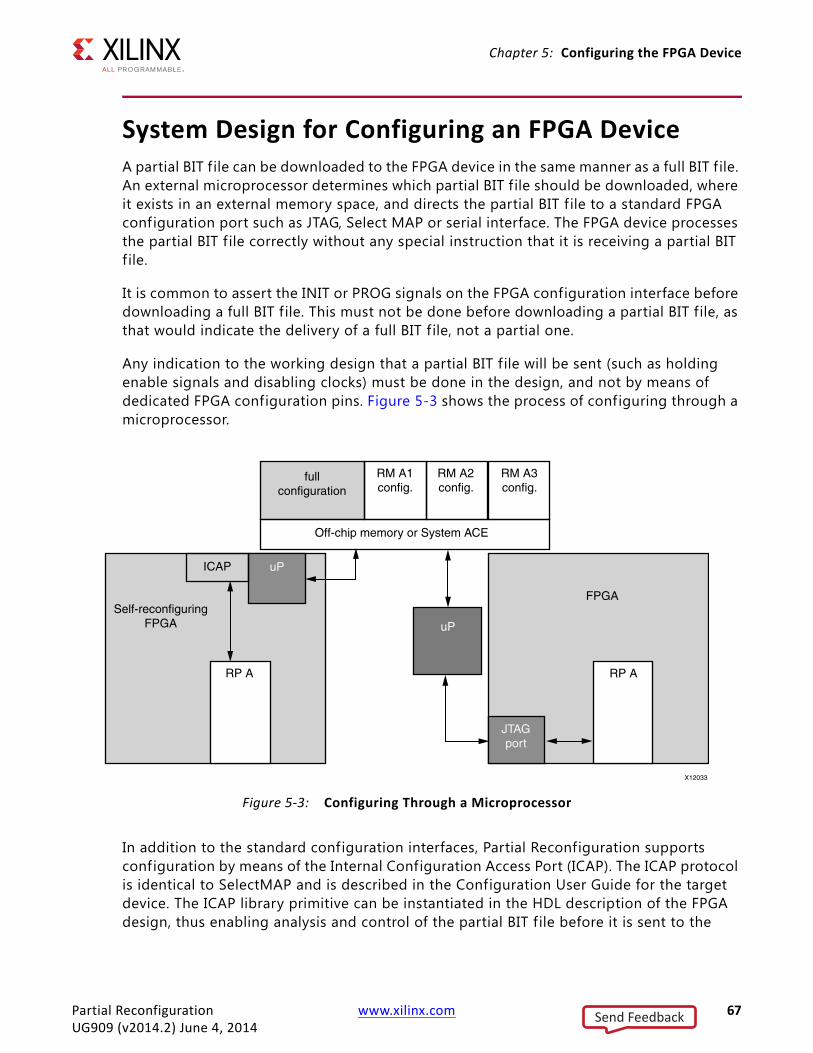
Chapter 5: Configuring the FPGA Device
System Design for Configuring an FPGA DeviceA partial BIT f ile can be downloaded to the FPGA device in the same manner as a full BIT f ile. An external microprocessor determines which partial BIT f ile should be downloaded, where it exists in an external memory space, and directs the partial BIT f ile to a standard FPGA configuration port such as JTAG, Select MAP or serial interface. The FPGA device processes the partial BIT f ile correctly without any special instruction that it is receiving a partial BIT f ile.
It is common to assert the INIT or PROG signals on the FPGA configuration interface before downloading a full BIT f ile. This must not be done before downloading a partial BIT f ile, as that would indicate the delivery of a full BIT f ile, not a partial one.
Any indication to the working design that a partial BIT f ile will be sent (such as holding enable signals and disabling clocks) must be done in the design, and not by means of dedicated FPGA configuration pins. Figure 5-3 shows the process of configuring through a microprocessor.
In addition to the standard configuration interfaces, Partial Reconfiguration supports configuration by means of the Internal Configuration Access Port (ICAP). The ICAP protocol is identical to SelectMAP and is described in the Configuration User Guide for the target device. The ICAP library primitive can be instantiated in the HDL description of the FPGA design, thus enabling analysis and control of the partial BIT f ile before it is sent to the
X-Ref Target - Figure 5-3
Figure 5-3: Configuring Through a Microprocessor
X12033
Self-reconfiguringFPGA
ICAP uP
uP
RP A
JTAGport
RP A
FPGA
fullconfiguration
RM A1config.
RM A2config.
RM A3config.
Off-chip memory or System ACE
Partial Reconfiguration www.xilinx.com 67UG909 (v2014.2) June 4, 2014
Send Feedback
Chapter 5: Configuring the FPGA Device
configuration port. The partial BIT f ile can be downloaded to the FPGA device through general purpose I/O or gigabit transceivers and then routed to the ICAP in the FPGA fabric.
The ICAP must be used, with an 8-bit bus only, for Partial Reconfiguration for encrypted 7 series BIT f iles. Reconfiguration through external configuration ports is not permitted when encryption is used.
Partial Bitstream CRC CheckingA partial bitstream is loaded into an active design, and the default built-in CRC check does not occur until the end of the bitstream. However, the configuration engine has the ability to perform a frame-by-frame CRC check and will not load a frame into the configuration memory if that CRC check fails. A failure is reported on the INIT_B pin (it is pulled low) and gives you the opportunity to take the next step: retry the partial bit f ile, fall back to a golden partial bit f ile, etc. The partially loaded reconfiguration region will not have valid programming in it, but the CRC check ensures the remainder of the device stays operational while the system recovers from the error.
This per-frame CRC check will be supported in an upcoming release of the Vivado® Design Suite. Without this dedicated silicon feature, recovery from errors in partial bitstreams cannot be guaranteed.
After a partial bit f ile has been loaded (with or without the per-frame CRC checks), the overall configuration of the device has changed. If the POST_CRC feature for SEU mitigation is enabled, the SEU mitigation engine will automatically recalculate the embedded SEU CRC value after partial bitstream has been loaded and the configuration interface has been desynced by the user. Upon completion of the CRC recalibration, FRAME_ECCE2's FRAME_VALID output will again toggle to indicate SEU detection has resumed.
Configuration FramesAll user-programmable features inside 7 series FPGA devices are controlled by volatile memory cells that must be configured at power-up. These memory cells are collectively known as configuration memory. They define the LUT equations, signal routing, IOB voltage standards, and all other aspects of the design.
7 series FPGA architectures have configuration memory arranged in frames that are tiled about the device. These frames are the smallest addressable segments of the device configuration memory space, and all operations must therefore act upon whole configuration frames.
Reconfigurable Frames are built upon these configuration frames, and these are the minimum building blocks for performing Partial Reconfiguration.
Partial Reconfiguration www.xilinx.com 68UG909 (v2014.2) June 4, 2014
Send Feedback
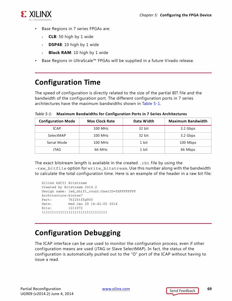
Chapter 5: Configuring the FPGA Device
• Base Regions in 7 series FPGAs are:
° CLB: 50 high by 1 wide
° DSP48: 10 high by 1 wide
° Block RAM: 10 high by 1 wide
• Base Regions in UltraScale™ FPGAs will be supplied in a future Vivado release.
Configuration TimeThe speed of configuration is directly related to the size of the partial BIT f ile and the bandwidth of the configuration port. The different configuration ports in 7 series architectures have the maximum bandwidths shown in Table 5-1.
The exact bitstream length is available in the created .rbt f ile by using the -raw_bitfile option for write_bitstream. Use this number along with the bandwidth to calculate the total configuration time. Here is an example of the header in a raw bit f ile:
Xilinx ASCII BitstreamCreated by Bitstream 2014.2Design name: led_shift_count;UserID=0XFFFFFFFFArchitecture:kintex7Part: 7k325tffg900Date: Wed Jan 29 16:42:05 2014Bits: 121107211111111111111111111111111111111
Configuration DebuggingThe ICAP interface can be use used to monitor the configuration process, even if other configuration means are used (JTAG or Slave SelectMAP). In fact, the status of the configuration is automatically pushed out to the “O” port of the ICAP without having to issue a read.
Table 5-1: Maximum Bandwidths for Configuration Ports in 7 Series Architectures
Configuration Mode Max Clock Rate Data Width Maximum Bandwidth
ICAP 100 MHz 32 bit 3.2 Gbps
SelectMAP 100 MHz 32 bit 3.2 Gbps
Serial Mode 100 MHz 1 bit 100 Mbps
JTAG 66 MHz 1 bit 66 Mbps
Partial Reconfiguration www.xilinx.com 69UG909 (v2014.2) June 4, 2014
Send Feedback
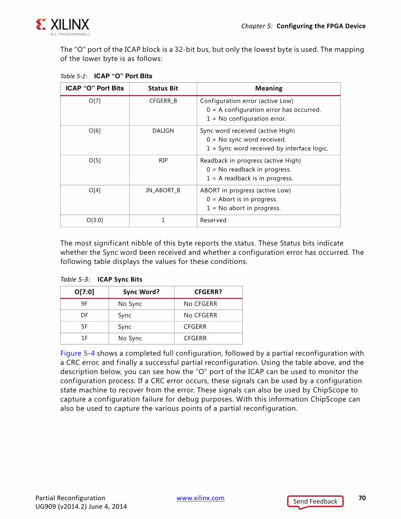
Chapter 5: Configuring the FPGA Device
The “O” port of the ICAP block is a 32-bit bus, but only the lowest byte is used. The mapping of the lower byte is as follows:
The most signif icant nibble of this byte reports the status. These Status bits indicate whether the Sync word been received and whether a configuration error has occurred. The following table displays the values for these conditions.
Figure 5-4 shows a completed full configuration, followed by a partial reconfiguration with a CRC error, and f inally a successful partial reconfiguration. Using the table above, and the description below, you can see how the “O” port of the ICAP can be used to monitor the configuration process. If a CRC error occurs, these signals can be used by a configuration state machine to recover from the error. These signals can also be used by ChipScope to capture a configuration failure for debug purposes. With this information ChipScope can also be used to capture the various points of a partial reconfiguration.
Table 5-2: ICAP “O” Port Bits
ICAP “O” Port Bits Status Bit Meaning
O[7] CFGERR_B Configuration error (active Low) 0 = A configuration error has occurred. 1 = No configuration error.
O[6] DALIGN Sync word received (active High) 0 = No sync word received. 1 = Sync word received by interface logic.
O[5] RIP Readback in progress (active High) 0 = No readback in progress. 1 = A readback is in progress.
O[4] IN_ABORT_B ABORT in progress (active Low) 0 = Abort is in progress. 1 = No abort in progress.
O[3:0] 1 Reserved
Table 5-3: ICAP Sync Bits
O[7:0] Sync Word? CFGERR?
9F No Sync No CFGERR
DF Sync No CFGERR
5F Sync CFGERR
1F No Sync CFGERR
Partial Reconfiguration www.xilinx.com 70UG909 (v2014.2) June 4, 2014
Send Feedback
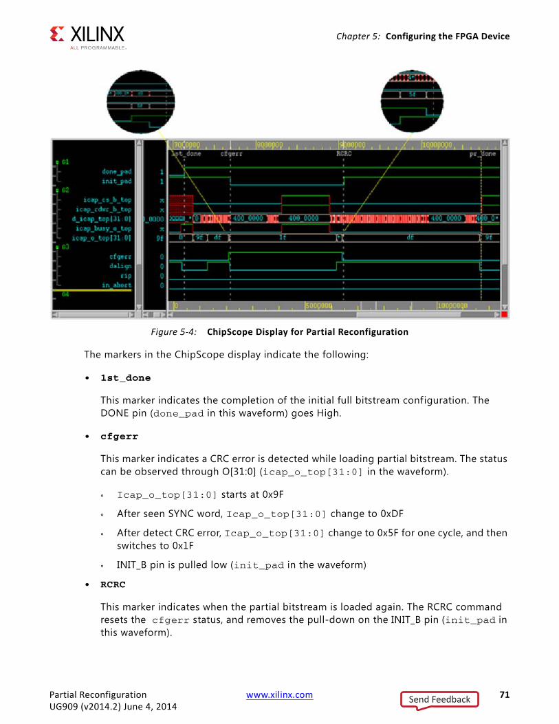
Chapter 5: Configuring the FPGA Device
The markers in the ChipScope display indicate the following:
• 1st_done
This marker indicates the completion of the initial full bitstream configuration. The DONE pin (done_pad in this waveform) goes High.
• cfgerr
This marker indicates a CRC error is detected while loading partial bitstream. The status can be observed through O[31:0] (icap_o_top[31:0] in the waveform).
° Icap_o_top[31:0] starts at 0x9F
° After seen SYNC word, Icap_o_top[31:0] change to 0xDF
° After detect CRC error, Icap_o_top[31:0] change to 0x5F for one cycle, and then switches to 0x1F
° INIT_B pin is pulled low (init_pad in the waveform)
• RCRC
This marker indicates when the partial bitstream is loaded again. The RCRC command resets the cfgerr status, and removes the pull-down on the INIT_B pin (init_pad in this waveform).
X-Ref Target - Figure 5-4
Figure 5-4: ChipScope Display for Partial Reconfiguration
Partial Reconfiguration www.xilinx.com 71UG909 (v2014.2) June 4, 2014
Send Feedback
Chapter 5: Configuring the FPGA Device
° Icap_o_top[31:0] change from 0x1F to 0x5F when the SYNC word is seen
° Icap_o_top[31:0] change from 0x5F to 0xDF when RCRC command is received
• pr_done
This marker indicates a successful Partial Reconfiguration.
° Icap_o_top[31:0] change from 0xDF to 0x9F when the DESYNC command is received and no configuration error is detected.
Partial Reconfiguration www.xilinx.com 72UG909 (v2014.2) June 4, 2014
Send Feedback
Chapter 6
Known Issues and Limitations
Known IssuesThis is a list of issues that may be encountered when using Partial Reconfiguration in the Vivado® 2014.2 release. If you encounter any of these issues, or discover any others, please inform Xilinx and send an example design that shows the issue. These test cases are very helpful for our efforts to improve the overall solution.
• Please report to Xilinx® all cases of fatal or internal errors, incomplete routing (partial antennas), or other rule violations that prevent place and route, pr_verify, and write_bitstream from succeeding. Including a design showing the failure is critical for proper analysis and implementation of f ixes.
• Reuse of implemented Reconfigurable Modules is not 100% preserved. In a future release, a checkpoint representing an implemented Reconfigurable Module could be saved from one configuration and then reused in another configuration. However, in the current release, the interface nets between the partition pins and the internal logic are not captured, so these signals must be rerouted.
° This can be done by running route_design after loading in a routed RM checkpoint. This process has not been extensively tested and is not recommended.
• If the initial configuration of an SSI device (7V2000T, 7VX1140T) is done through an SPI interface, partial bitstreams cannot be delivered to the master (or any) ICAP; they must be delivered to an external port, such as JTAG. If the initial configuration is done through any other configuration port, the master ICAP can be used as the delivery port for partial bitstreams.
° Please contact Xilinx Support for a workaround.
• Do not drive multiple outputs of a single Reconfigurable Module with the same source. Each output of an RM must have a unique driver.
• When using SNAPPING_MODE in conjunction with RESET_AFTER_RECONFIG, the derived ranges will correctly include the necessary sites. However, the shading region shown in the GUI will not correctly show the sites owned by the Pblock that are outside of the original Pblock rectangle.
Partial Reconfiguration www.xilinx.com 73UG909 (v2014.2) June 4, 2014
Send Feedback
Chapter 6: Known Issues and Limitations
Known LimitationsCertain features are not yet developed or supported in Vivado 2014.2. Some of these features may be added in upcoming releases. These include:
• When selecting Pblock ranges to define the size and shape of the Reconfigurable Partition, do not use the CLOCKREGION resource type. Pblock ranges must only include types SLICE, RAMB18, RAMB36, and DSP48 resource types.
• Project support. Compiling configurations using projects and project commands (create_run, launch_runs, etc.) is not yet supported. Managing PR projects in the Vivado IDE is likewise not yet supported.
° Checkpoints can be opened in the IDE and many analysis features can be used, but the Design Runs features cannot be used.
• Implementation directives (the -directive option for opt_design, place_design, phys_opt_design, and route_design) are supported, but the “Explore” value is not recommended for route_design. This option calls place_design behind the scenes and has not yet been tuned for Partial Reconfiguration.
• Using phys_opt_design on a routed checkpoint is not supported.
• The per-frame CRC check feature for write_bitstream has not yet been implemented. This feature is scheduled to be added in a future software release.
• Do not use Vivado Debug core insertion features within Reconfigurable Partitions. This flow inserts the debug hub, which includes BSCAN and BUFG primitives, which are not permitted inside reconfigurable bitstreams.
• Do not use Partial Reconfiguration with Tandem Configuration capabilities within Xilinx PCIe IP.
Partial Reconfiguration www.xilinx.com 74UG909 (v2014.2) June 4, 2014
Send Feedback
Appendix A
Additional Resources and Legal Notices
Xilinx ResourcesFor support resources such as Answers, Documentation, Downloads, and Forums, see Xilinx Support.
Solution CentersSee the Xilinx Solution Centers for support on devices, software tools, and intellectual property at all stages of the design cycle. Topics include design assistance, advisories, and troubleshooting tips.
References1. 7 Series FPGAs Configuration User Guide (UG470)
2. Zynq-7000 All Programmable SoC Technical Reference Manual (UG585)
3. Partial Reconfiguration User Guide (UG702) - For ISE Design Tools
4. Hierarchical Design Methodology Guide (UG748) - For ISE Design Tools
5. Repeatable Results with Design Preservation (WP362) - For ISE Design Tools
6. UltraFast Design Methodology Guide for the Vivado Design Suite (UG949)
7. 7 Series FPGAs Integrated Block for PCI Express Product Guide(PG054)
8. Virtex-7 FPGA Gen3 Integrated Block for PCI Express Product Guide(PG023)
9. UltraFast Design Methodology Guide for the Vivado Design Suite (UG949)
10. Vivado Design Suite Tutorial: Partial Reconfiguration (UG947)
11. Vivado Design Suite Tcl Command Reference Guide (UG835)
12. XST User Guide for Virtex-6, Spartan-6, and 7 Series Devices (UG687)
Partial Reconfiguration www.xilinx.com 75UG909 (v2014.2) June 4, 2014
Send Feedback
Appendix A: Additional Resources and Legal Notices
13. Vivado Design Suite User Guide: Synthesis (UG901)
14. Vivado Design Suite User Guide: Using Constraints (UG903)
15. Vivado Design Suite User Guide: Design Analysis and Closure Techniques (UG906)
16. 7 Series FPGAs GTX/GTH Transceivers User Guide (UG476)
17. MMCM and PLL Dynamic Reconfiguration (7 Series) (XAPP888)
18. PRC/EPRC: Data Integrity and Security Controller for Partial Reconfiguration (XAPP887)
19. Vivado Design Suite User Guide: Programming and Debugging (UG908)
20. Bitstream Identification with USR_ACCESS (XAPP497)
21. Zynq-7000 AP SoC Technical Reference Manual (UG585)
22. Vivado Design Suite QuickTake Video Tutorials
23. Vivado Design Suite Documentation
Please Read: Important Legal NoticesThe information disclosed to you hereunder (the “Materials”) is provided solely for the selection and use of Xilinx products. To the maximum extent permitted by applicable law: (1) Materials are made available "AS IS" and with all faults, Xilinx hereby DISCLAIMS ALL WARRANTIES AND CONDITIONS, EXPRESS, IMPLIED, OR STATUTORY, INCLUDING BUT NOT LIMITED TO WARRANTIES OF MERCHANTABILITY, NON-INFRINGEMENT, OR FITNESS FOR ANY PARTICULAR PURPOSE; and (2) Xilinx shall not be liable (whether in contract or tort, including negligence, or under any other theory of liability) for any loss or damage of any kind or nature related to, arising under, or in connection with, the Materials (including your use of the Materials), including for any direct, indirect, special, incidental, or consequential loss or damage (including loss of data, profits, goodwill, or any type of loss or damage suffered as a result of any action brought by a third party) even if such damage or loss was reasonably foreseeable or Xilinx had been advised of the possibility of the same. Xilinx assumes no obligation to correct any errors contained in the Materials or to notify you of updates to the Materials or to product specifications. You may not reproduce, modify, distribute, or publicly display the Materials without prior written consent. Certain products are subject to the terms and conditions of Xilinx’s limited warranty, please refer to Xilinx’s Terms of Sale which can be viewed at http://www.xilinx.com/legal.htm#tos; IP cores may be subject to warranty and support terms contained in a license issued to you by Xilinx. Xilinx products are not designed or intended to be fail-safe or for use in any application requiring fail-safe performance; you assume sole risk and liability for use of Xilinx products in such critical applications, please refer to Xilinx’s Terms of Sale which can be viewed at http://www.xilinx.com/legal.htm#tos.© Copyright 2012–2014 Xilinx, Inc. Xilinx, the Xilinx logo, Artix, ISE, Kintex, Spartan, Virtex, Vivado, Zynq, and other designated brands included herein are trademarks of Xilinx in the United States and other countries. All other trademarks are the property of their respective owners.
Partial Reconfiguration www.xilinx.com 76UG909 (v2014.2) June 4, 2014
Send Feedback