Embed Size (px)
Citation preview
Vivado Design Suite Tutorial:
Model-Based DSP Design using System Generator
UG948 (v2014.1) May 20, 2014
This tutorial document has been validated for the following software versions: Vivado Design Suite 2014.1This tutorial document has been validated for the following software versions: Vivado Design Suite 2014.1This tutorial document has been validated for the following software versions: Vivado Design Suite 2014.1This tutorial document has been validated for the following software versions: Vivado Design Suite 2014.1and 2014.2.and 2014.2.and 2014.2.and 2014.2.
Notice of Disclaimer The information disclosed to you hereunder (the "Materials") is provided solely for the selection and use of Xilinx products. To the maximum extent permitted by applicable law: (1) Materials are made available "AS IS" and with all faults, Xilinx hereby DISCLAIMS ALL WARRANTIES AND CONDITIONS, EXPRESS, IMPLIED, OR STATUTORY, INCLUDING BUT NOT LIMITED TO WARRANTIES OF MERCHANTABILITY, NON-INFRINGEMENT, OR FITNESS FOR ANY PARTICULAR PURPOSE; and (2) Xilinx shall not be liable (whether in contract or tort, including negligence, or under any other theory of liability) for any loss or damage of any kind or nature related to, arising under, or in connection with, the Materials (including your use of the Materials), including for any direct, indirect, special, incidental, or consequential loss or damage (including loss of data, profits, goodwill, or any type of loss or damage suffered as a result of any action brought by a third party) even if such damage or loss was reasonably foreseeable or Xilinx had been advised of the possibility of the same. Xilinx assumes no obligation to correct any errors contained in the Materials or to notify you of updates to the Materials or to product specifications. You may not reproduce, modify, distribute, or publicly display the Materials without prior written consent. Certain products are subject to the terms and conditions of the Limited Warranties which can be viewed at http://www.xilinx.com/warranty.htm; IP cores may be subject to warranty and support terms contained in a license issued to you by Xilinx. Xilinx products are not designed or intended to be fail-safe or for use in any application requiring fail-safe performance; you assume sole risk and liability for use of Xilinx products in Critical Applications: http://www.xilinx.com/warranty.htm#critapps.
©Copyright 2014 Xilinx, Inc. Xilinx, the Xilinx logo, Artix, ISE, Kintex, Spartan, Virtex, Zynq, and other designated brands included herein are trademarks of Xilinx in the United States and other countries. All other trademarks are the property of their respective owners.
Revision History The following table shows the revision history for this document.
Date Version Changes
05/20/2014 2014.1 Added Lab 11 titled Black Box Examples
12/18/2013 2013.4 No technical updates. Re-published for this release
10/02/2013 2013.3 Added Lab 10 titled AXI4-Lite Interface Synthesis
6/19/2013 2013.2 Added Lab 9 titled “Including a System Generator Design as a Module in an IP Integrator Design
3/20/2013 2013.1 Initial Xilinx Release
Send Feedback
Model-Based DSP Design using System Generatorwww.xilinx.com 3 UG948 (v2014.1) May 20, 2014
Table of Contents
Vivado Design Suite Tutorial: ................................................................................. 1
Revision History ................................................................................................................................................................ 2
Chapter 1 System Generator for DSP Overview ..............................................................................6
Introduction ....................................................................................................................................................................... 6
Software Requirements .................................................................................................................................................... 7
Hardware Requirements .................................................................................................................................................. 7
Configuring MATLAB to the Vivado® Design Suite..................................................................................................... 7
Locating and Preparing the Tutorial Design Files ......................................................................................................... 8
Lab 1: Using Simulink .............................................................................................................................9
Introduction ....................................................................................................................................................................... 9
Part 1: Introduction to Simulink ...................................................................................................................................... 9
Part 2: Analyzing the Sampling Period Effect .............................................................................................................. 16
Part 3: Creating a Simple Filter Design Using Simulink Blocks ................................................................................. 16
Part 4: Creating a Subsystem ........................................................................................................................................ 17
Summary .......................................................................................................................................................................... 19
Lab 2: Design Creation Basics .............................................................................................................. 20
Introduction ..................................................................................................................................................................... 20
Objectives ........................................................................................................................................................................ 20
Procedure......................................................................................................................................................................... 20
Part 1: Simulate the Executable Specification ............................................................................................................. 21
Part 2: Duplicate the Design using Xilinx Blocks ......................................................................................................... 21
Part 3: Implement the Xilinx Design ............................................................................................................................. 23
Part 4: Explore Different Hardware Architectures ....................................................................................................... 26
Solution ............................................................................................................................................................................ 29
Lab 3: Signal Routing ........................................................................................................................... 30
Introduction ..................................................................................................................................................................... 30
Objectives ........................................................................................................................................................................ 30
Part 1: Designing Padding Logic ................................................................................................................................... 30
Send Feedback
Model-Based DSP Design using System Generatorwww.xilinx.com 4 UG948 (v2014.1) May 20, 2014
Part 2: Designing Unpadding Logic .............................................................................................................................. 32
Solution ............................................................................................................................................................................ 33
Lab 4: System Control .......................................................................................................................... 34
Introduction ..................................................................................................................................................................... 34
Objectives ........................................................................................................................................................................ 34
Procedure......................................................................................................................................................................... 34
Solution ............................................................................................................................................................................ 37
Lab 5: Multi-Rate Systems ................................................................................................................... 38
Lab 5 Introduction .......................................................................................................................................................... 38
Objectives ........................................................................................................................................................................ 38
Part 1: Changing Sample Rate ...................................................................................................................................... 38
Part 2: Using Serial-to-Parallel Blocks .......................................................................................................................... 41
Part 3: Using Parallel-to-Serial Blocks .......................................................................................................................... 42
Solution ............................................................................................................................................................................ 42
Lab 6: Using Memories ......................................................................................................................... 43
Lab 6 Introduction .......................................................................................................................................................... 43
Objectives ........................................................................................................................................................................ 43
Procedure......................................................................................................................................................................... 43
Solution ............................................................................................................................................................................ 46
Lab 7: Including a System Generator Model in a Vivado IDE Design .............................................. 47
Lab 7 Introduction .......................................................................................................................................................... 47
Part 1: Create a new Vivado IDE Project and add RTL/DSP sources and XDC constraints .................................... 47
Part 2: Interacting with the DSP Module from the Vivado IDE Cockpit ................................................................... 52
Lab 8: Importing C/C++ Source Files into System Generator by Leveraging Integration with Vivado HLS ............................................................................................................................................ 55
Lab 8 Introduction .......................................................................................................................................................... 55
Part 1: Creating a System Generator Package from Vivado HLS .............................................................................. 55
Part 2: Including a Vivado HLS Package in a System Generator Design ................................................................. 58
Lab 9: Including a System Generator Design as a Module in an IP Integrator Design .................. 62
Lab 9 Introduction .......................................................................................................................................................... 62
Part 1: Using the IP Catalog as a Compilation Target ................................................................................................ 62
Part 2: Generating Output Products ............................................................................................................................. 64
Part 3: IP Creation Modes .............................................................................................................................................. 65
Send Feedback
Model-Based DSP Design using System Generatorwww.xilinx.com 5 UG948 (v2014.1) May 20, 2014
Part 4: Port/Pin Interface Packaging ............................................................................................................................. 65
Part 5: Port-Name Group-Based Interface Inference ................................................................................................. 67
Part 6: Compiling the gain_control Design .................................................................................................................. 69
Part 6: Verifying the gain_control Design .................................................................................................................... 72
Lab 10: Packaging a Synthesized AXI4-Lite Interface ....................................................................... 77
Lab 10 Introduction ........................................................................................................................................................ 77
Requirements .................................................................................................................................................................. 77
Procedure......................................................................................................................................................................... 78
Conclusion ....................................................................................................................................................................... 86
Lab 11: Black Box Examples................................................................................................................. 87
Example 1 – Importing VHDL into a Black Box ........................................................................................................... 87
Send Feedback
Model-Based DSP Design using System Generatorwww.xilinx.com 6 UG948 (v2014.1) May 20, 2014
Chapter 1 System Generator for DSP Overview
Introduction The System Generator for DSP is a design tool in the Vivado® Design Suite that enables you to use the MathWorks® model-based Simulink® design environment for FPGA design. Previous experience with Xilinx® FPGA devices or RTL design methodologies is not required when using System Generator. Designs are captured in the Simulink™ modeling environment using a Xilinx-specific block set. Downstream FPGA implementation steps including RTL synthesis and Place and Route are automatically performed to produce an FPGA programming bitstream.
Over 80 building blocks are included in a Xilinx-specific DSP block set for Simulink. These blocks include common building blocks such as adders, multipliers and registers. Also included are complex DSP building blocks such as forward-error-correction blocks, FFTs, filters and memories. These blocks leverage Xilinx LogiCORE™ IP to produce optimized results for the selected target device.
In this tutorial, you will do the following:
• Lab 1: Use Simulink to create a simple design, create a subsystem, and then simulate.
• Lab 2: Build a basic design in System Generator, simulate the design, and then generate an FPGA bitstream for a target Xilinx technology.
• Lab 3: Learn how signal routing blocks are used to re-define or modify fixed-point numbers at the bit-level.
• Lab 4: Create a finite state machine using the Mcode block in System Generator.
• Lab 5: Change sample rates in a multi-rate DSP design and then convert a serial data stream to a parallel data word and a parallel data word to a serial data stream.
• Lab 6: Use a Xilinx ROM block to implement a trig or math function such as arcsin.
• Lab 7: Include a System Generator model within a Vivado IDE design and combine that model with other RTL sources.
• Lab 8: Import C/C++ source files into a System Generator model by leveraging the tool integration with Vivado High-Level Synthesis (HLS).
• Lab 9: Including a System Generator Design as a Module in an IP Integrator Design
• Lab 10: AXI4-Lite Interface Synthesis
• Lab 11: Black Box Examples
Send Feedback
Software Requirements
Model-Based DSP Design using System Generatorwww.xilinx.com 7 UG948 (v2014.1) May 20, 2014
Software Requirements The lab exercises in this tutorial require the installation of MATLAB 2013b (or later) and Vivado Design Suite 2014.1 (or later).
Hardware Requirements The supported Operating Systems include Redhat 5.6 Linux 64, Windows 7 and Windows XP (32 and 64 bit). Xilinx recommends a minimum of 2 GB of RAM when using the Vivado Design Suite.
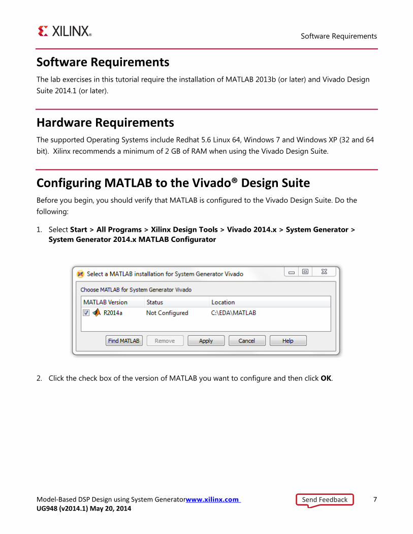
Configuring MATLAB to the Vivado® Design Suite Before you begin, you should verify that MATLAB is configured to the Vivado Design Suite. Do the following:
1. Select Start > All Programs > Xilinx Design Tools > Vivado 2014.x > System Generator > System Generator 2014.x MATLAB Configurator
2. Click the check box of the version of MATLAB you want to configure and then click OK.
Send Feedback
Locating and Preparing the Tutorial Design Files
Model-Based DSP Design using System Generatorwww.xilinx.com 8 UG948 (v2014.1) May 20, 2014
Locating and Preparing the Tutorial Design Files There are separate project files and sources for each of the labs in this tutorial. You can find the design files for this tutorial under Vivado Design Suite -2014.1 Tutorials on the Xilinx.com website.
Download the ug948-design-files.zip file from the Xilinx website. 1.
Extract the zip file contents into any write-accessible location on your hard drive, or network 2.location.
RECOMMENDED: You will modify the tutorial design data while working through this tutorial. You should use a new copy of the ug948-design-files directory each time you start this tutorial.
Send Feedback
Model-Based DSP Design using System Generatorwww.xilinx.com 9 UG948 (v2014.1) May 20, 2014
Lab 1: Using Simulink
Introduction In this lab exercise, you will learn the basics of Simulink. You will use a Simulink block set to generate a simple design and take it through simulation. You will then change the sampling settings to see its effect on the output. You will then learn how to create a subsystem.
Objectives After completing this lab, you will be able to:
• Use the Simulink tool to create a simple design
• Create a subsystem and simulate
• Describe the effect of the sampling period
Procedure This exercise has four primary parts. In Step 1, you are introduced to the Simulink environment. In Step 2, you will analyze the effect of the sampling period. In Step 3, you will create a simple filter design using a Simulink block set. Finally, in Step 4, you will create a subsystem of the design and perform simulation.
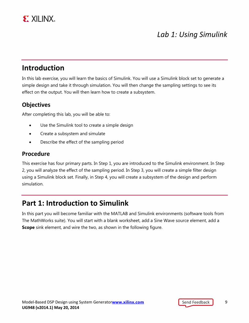
Part 1: Introduction to Simulink In this part you will become familiar with the MATLAB and Simulink environments (software tools from The MathWorks suite). You will start with a blank worksheet, add a Sine Wave source element, add a Scope sink element, and wire the two, as shown in the following figure.
Send Feedback
Part 1: Introduction to Simulink
Model-Based DSP Design using System Generatorwww.xilinx.com 10 UG948 (v2014.1) May 20, 2014
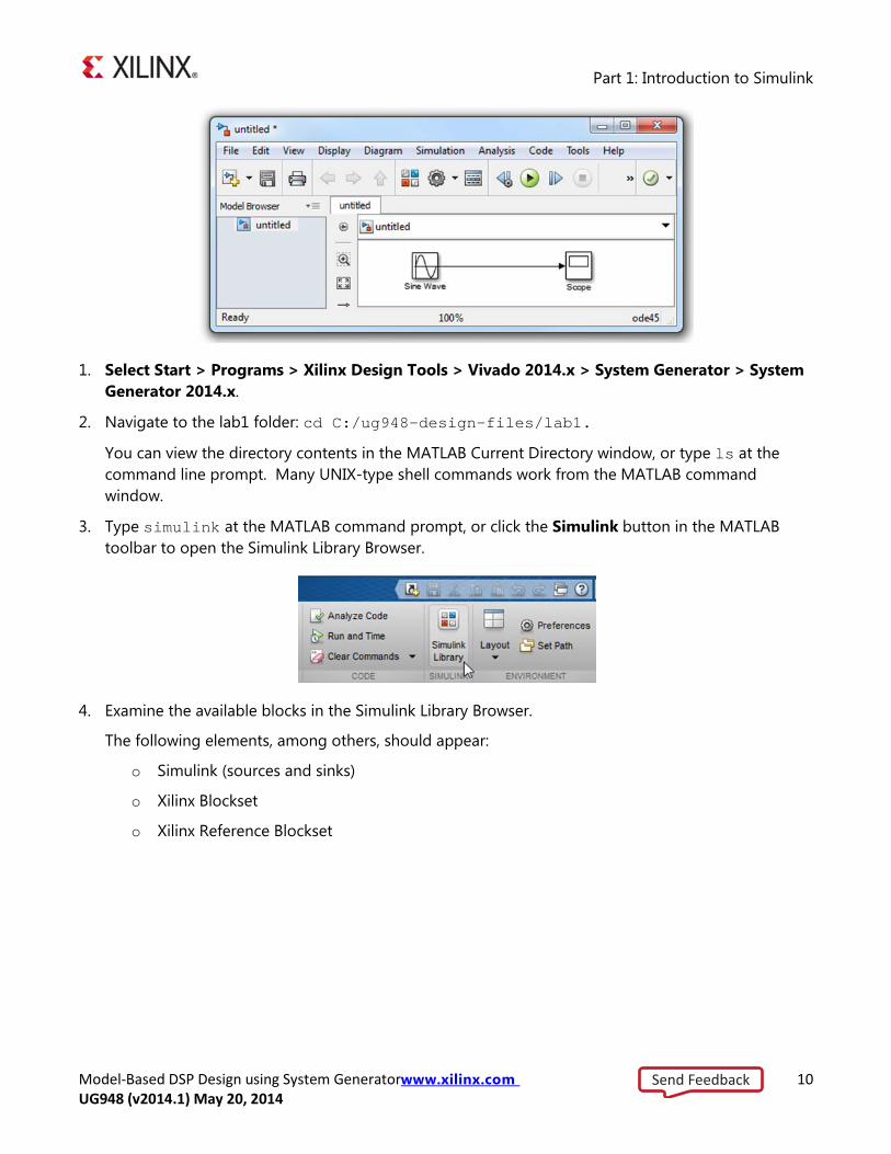
1. Select Start > Programs > Xilinx Design Tools > Vivado 2014.x > System Generator > System Generator 2014.x.
2. Navigate to the lab1 folder: cd C:/ug948-design-files/lab1.
You can view the directory contents in the MATLAB Current Directory window, or type ls at the command line prompt. Many UNIX-type shell commands work from the MATLAB command window.
3. Type simulink at the MATLAB command prompt, or click the Simulink button in the MATLAB toolbar to open the Simulink Library Browser.
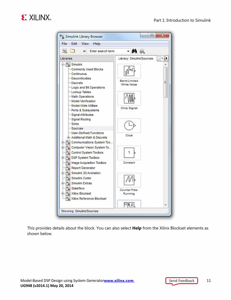
4. Examine the available blocks in the Simulink Library Browser.
The following elements, among others, should appear:
o Simulink (sources and sinks)
o Xilinx Blockset
o Xilinx Reference Blockset
Send Feedback
Part 1: Introduction to Simulink
Model-Based DSP Design using System Generatorwww.xilinx.com 11 UG948 (v2014.1) May 20, 2014
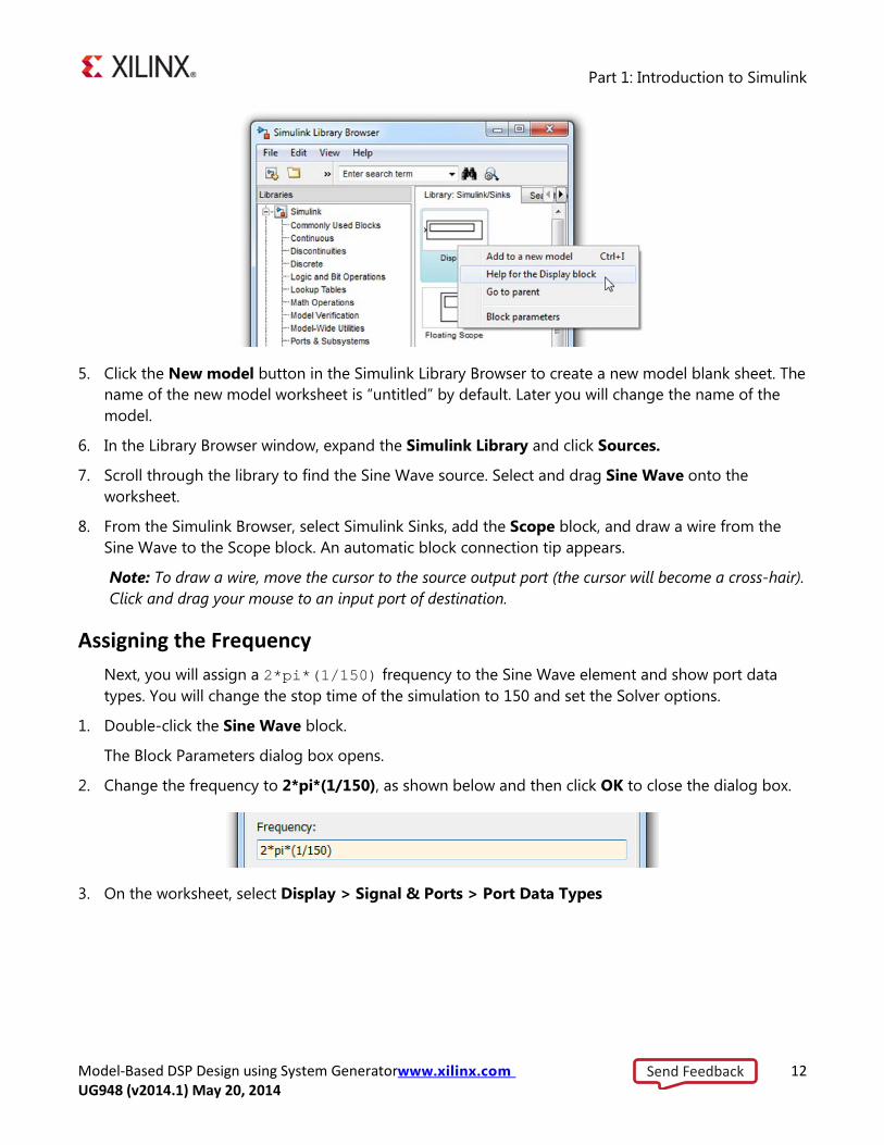
This provides details about the block. You can also select Help from the Xilinx Blockset elements as shown below.
Send Feedback
Part 1: Introduction to Simulink
Model-Based DSP Design using System Generatorwww.xilinx.com 12 UG948 (v2014.1) May 20, 2014
5. Click the New model button in the Simulink Library Browser to create a new model blank sheet. The name of the new model worksheet is “untitled” by default. Later you will change the name of the model.
6. In the Library Browser window, expand the Simulink Library and click Sources.
7. Scroll through the library to find the Sine Wave source. Select and drag Sine Wave onto the worksheet.
8. From the Simulink Browser, select Simulink Sinks, add the Scope block, and draw a wire from the Sine Wave to the Scope block. An automatic block connection tip appears.
Note: To draw a wire, move the cursor to the source output port (the cursor will become a cross-hair). Click and drag your mouse to an input port of destination.
Assigning the Frequency Next, you will assign a 2*pi*(1/150) frequency to the Sine Wave element and show port data types. You will change the stop time of the simulation to 150 and set the Solver options.
1. Double-click the Sine Wave block.
The Block Parameters dialog box opens.
2. Change the frequency to 2*pi*(1/150), as shown below and then click OK to close the dialog box.
3. On the worksheet, select Display > Signal & Ports > Port Data Types
Send Feedback
Part 1: Introduction to Simulink
Model-Based DSP Design using System Generatorwww.xilinx.com 13 UG948 (v2014.1) May 20, 2014
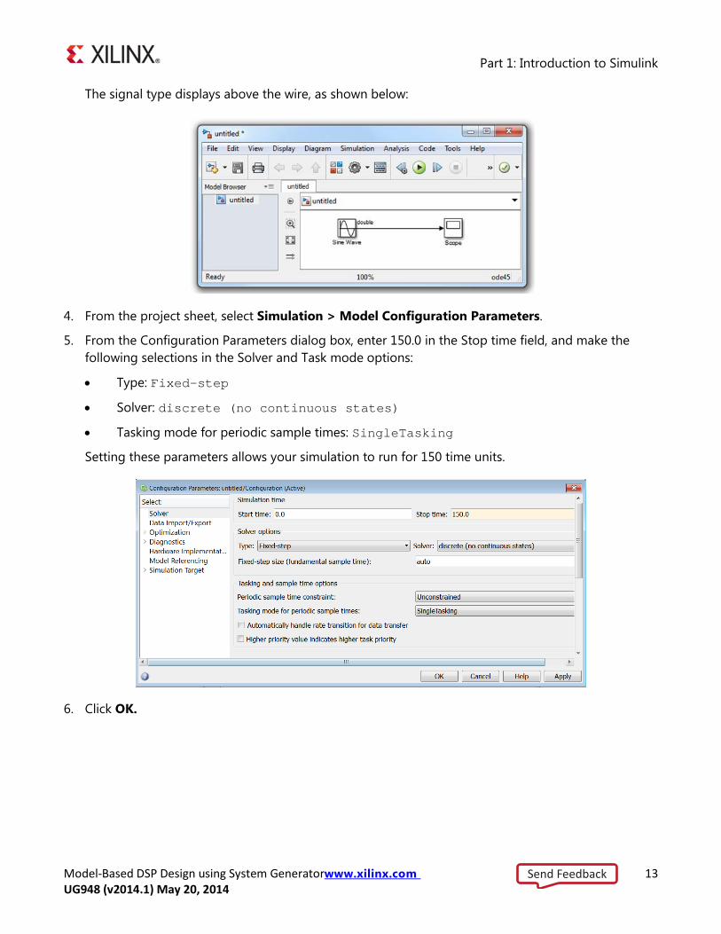
The signal type displays above the wire, as shown below:
4. From the project sheet, select Simulation > Model Configuration Parameters.
5. From the Configuration Parameters dialog box, enter 150.0 in the Stop time field, and make the following selections in the Solver and Task mode options:
• Type: Fixed-step
• Solver: discrete (no continuous states)
• Tasking mode for periodic sample times: SingleTasking
Setting these parameters allows your simulation to run for 150 time units.
6. Click OK.
Send Feedback
Part 1: Introduction to Simulink
Model-Based DSP Design using System Generatorwww.xilinx.com 14 UG948 (v2014.1) May 20, 2014
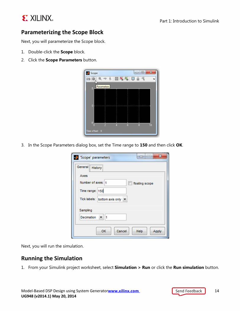
Parameterizing the Scope Block Next, you will parameterize the Scope block.
1. Double-click the Scope block.
2. Click the Scope Parameters button.
3. In the Scope Parameters dialog box, set the Time range to 150 and then click OK.
Next, you will run the simulation.
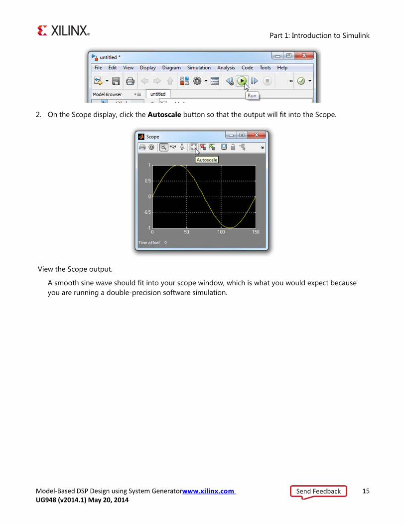
Running the Simulation 1. From your Simulink project worksheet, select Simulation > Run or click the Run simulation button.
Send Feedback
Part 1: Introduction to Simulink
Model-Based DSP Design using System Generatorwww.xilinx.com 15 UG948 (v2014.1) May 20, 2014
2. On the Scope display, click the Autoscale button so that the output will fit into the Scope.
View the Scope output.
A smooth sine wave should fit into your scope window, which is what you would expect because you are running a double-precision software simulation.
Send Feedback
Part 2: Analyzing the Sampling Period Effect
Model-Based DSP Design using System Generatorwww.xilinx.com 16 UG948 (v2014.1) May 20, 2014
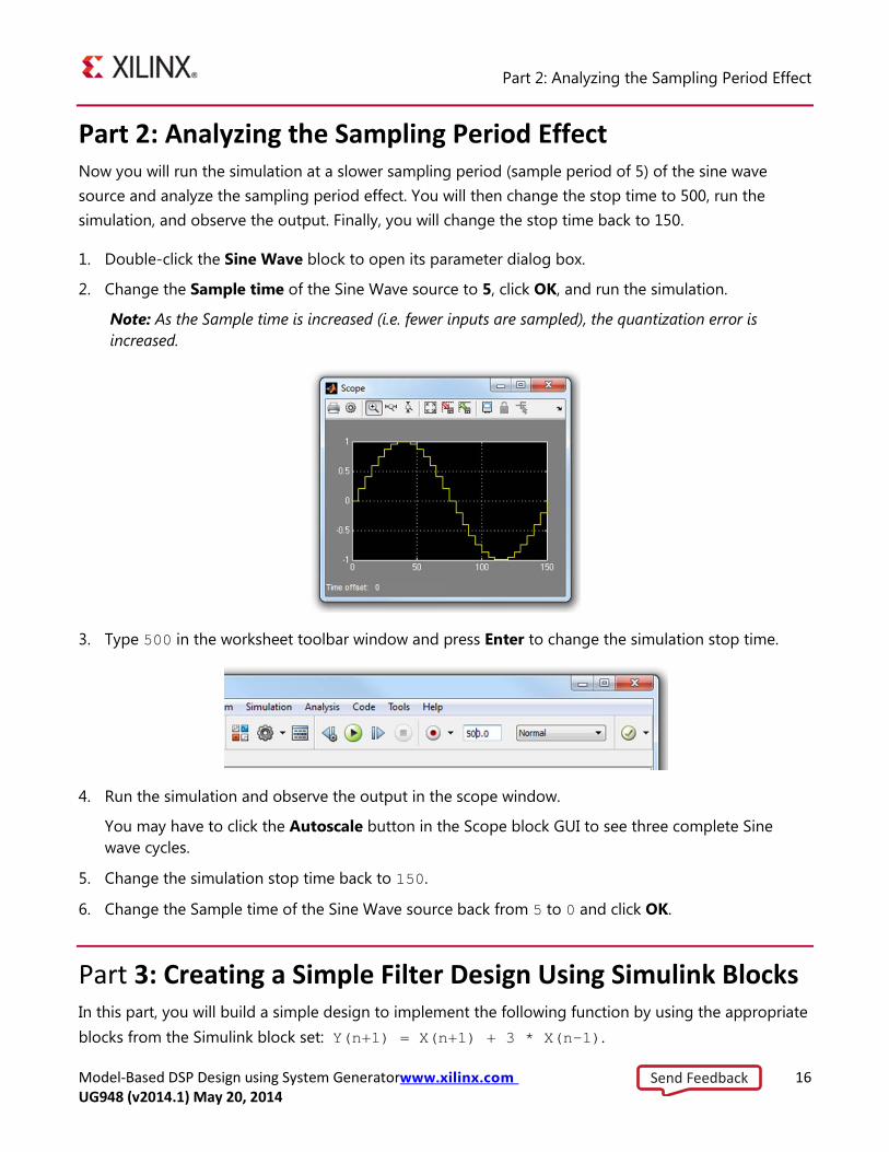
Part 2: Analyzing the Sampling Period Effect Now you will run the simulation at a slower sampling period (sample period of 5) of the sine wave source and analyze the sampling period effect. You will then change the stop time to 500, run the simulation, and observe the output. Finally, you will change the stop time back to 150.
1. Double-click the Sine Wave block to open its parameter dialog box.
2. Change the Sample time of the Sine Wave source to 5, click OK, and run the simulation.
Note: As the Sample time is increased (i.e. fewer inputs are sampled), the quantization error is increased.
3. Type 500 in the worksheet toolbar window and press Enter to change the simulation stop time.
4. Run the simulation and observe the output in the scope window.
You may have to click the Autoscale button in the Scope block GUI to see three complete Sine wave cycles.
5. Change the simulation stop time back to 150.
6. Change the Sample time of the Sine Wave source back from 5 to 0 and click OK.
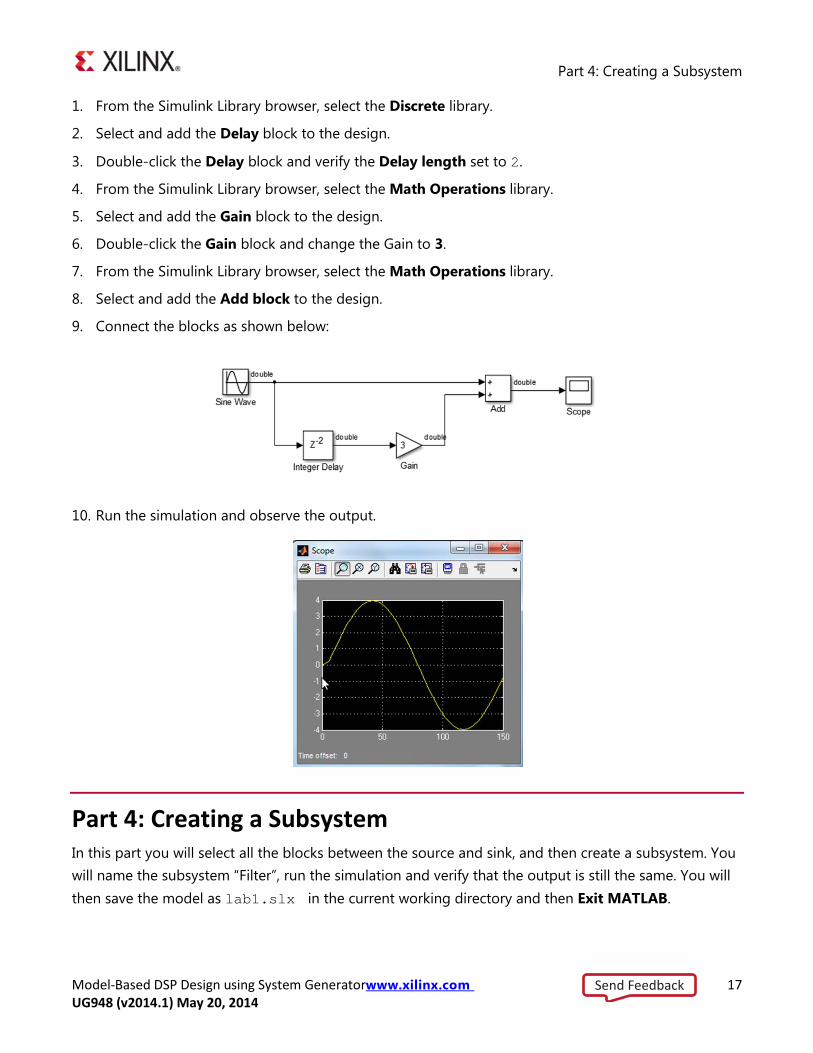
Part 3: Creating a Simple Filter Design Using Simulink Blocks In this part, you will build a simple design to implement the following function by using the appropriate blocks from the Simulink block set: Y(n+1) = X(n+1) + 3 * X(n-1).
Send Feedback
Part 4: Creating a Subsystem
Model-Based DSP Design using System Generatorwww.xilinx.com 17 UG948 (v2014.1) May 20, 2014
1. From the Simulink Library browser, select the Discrete library.
2. Select and add the Delay block to the design.
3. Double-click the Delay block and verify the Delay length set to 2.
4. From the Simulink Library browser, select the Math Operations library.
5. Select and add the Gain block to the design.
6. Double-click the Gain block and change the Gain to 3.
7. From the Simulink Library browser, select the Math Operations library.
8. Select and add the Add block to the design.
9. Connect the blocks as shown below:
10. Run the simulation and observe the output.
Part 4: Creating a Subsystem In this part you will select all the blocks between the source and sink, and then create a subsystem. You will name the subsystem “Filter”, run the simulation and verify that the output is still the same. You will then save the model as lab1.slx in the current working directory and then Exit MATLAB.
Send Feedback
Part 4: Creating a Subsystem
Model-Based DSP Design using System Generatorwww.xilinx.com 18 UG948 (v2014.1) May 20, 2014
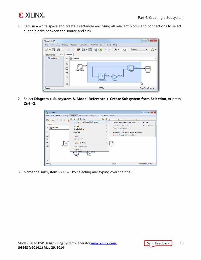
1. Click in a white space and create a rectangle enclosing all relevant blocks and connections to select all the blocks between the source and sink.
2. Select Diagram > Subsystem & Model Reference > Create Subsystem from Selection, or press Ctrl+G.
3. Name the subsystem Filter by selecting and typing over the title.
Send Feedback
Summary
Model-Based DSP Design using System Generatorwww.xilinx.com 19 UG948 (v2014.1) May 20, 2014
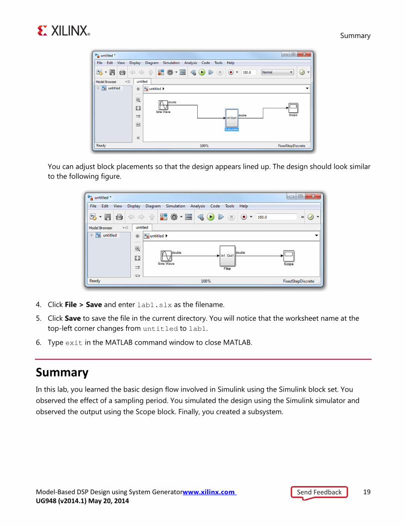
You can adjust block placements so that the design appears lined up. The design should look similar to the following figure.
4. Click File > Save and enter lab1.slx as the filename.
5. Click Save to save the file in the current directory. You will notice that the worksheet name at the top-left corner changes from untitled to lab1.
6. Type exit in the MATLAB command window to close MATLAB.
Summary In this lab, you learned the basic design flow involved in Simulink using the Simulink block set. You observed the effect of a sampling period. You simulated the design using the Simulink simulator and observed the output using the Scope block. Finally, you created a subsystem.
Send Feedback
Model-Based DSP Design using System Generatorwww.xilinx.com 20 UG948 (v2014.1) May 20, 2014
Lab 2: Design Creation Basics
Introduction This lab exercise will introduce you to the basic concepts of creating a design using System Generator for DSP within the model-based design flow provided through Simulink. The design is a simple multiply-add circuit.
Objectives After completing this lab, you will be able to:
• Simulate a design in System Generator for DSP
• Run the System Generator token to generate a Xilinx FPGA bitstream
• Create a subsystem
• Improve performance using dedicated Xilinx FPGA math functions
Procedure This lab has four primary parts. In part 1, you open and simulate a Simulink block set-based design that serves as an ”executable specification”. In Part 2, you re-create the Simulink design using the Xilinx block set. In Part 3, you take the Xilinx executable specification through the full implementation flow. Finally, in Part 4, you explore different hardware architectures to achieve the best performance.
Send Feedback
Part 1: Simulate the Executable Specification
Model-Based DSP Design using System Generatorwww.xilinx.com 21 UG948 (v2014.1) May 20, 2014
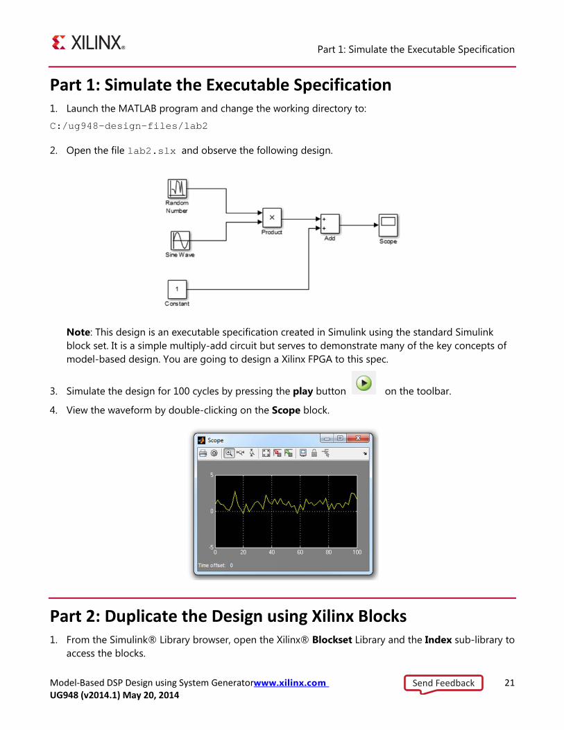
Part 1: Simulate the Executable Specification 1. Launch the MATLAB program and change the working directory to:
C:/ug948-design-files/lab2
2. Open the file lab2.slx and observe the following design.
Note: This design is an executable specification created in Simulink using the standard Simulink block set. It is a simple multiply-add circuit but serves to demonstrate many of the key concepts of model-based design. You are going to design a Xilinx FPGA to this spec.
3. Simulate the design for 100 cycles by pressing the play button on the toolbar.
4. View the waveform by double-clicking on the Scope block.
Part 2: Duplicate the Design using Xilinx Blocks 1. From the Simulink® Library browser, open the Xilinx® Blockset Library and the Index sub-library to
access the blocks.
Send Feedback
Part 2: Duplicate the Design using Xilinx Blocks
Model-Based DSP Design using System Generatorwww.xilinx.com 22 UG948 (v2014.1) May 20, 2014
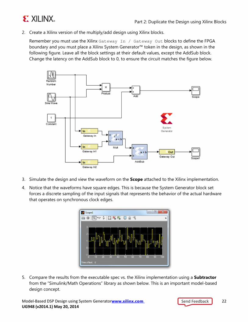
2. Create a Xilinx version of the multiply/add design using Xilinx blocks.
Remember you must use the Xilinx Gateway In / Gateway Out blocks to define the FPGA boundary and you must place a Xilinx System Generator™ token in the design, as shown in the following figure. Leave all the block settings at their default values, except the AddSub block. Change the latency on the AddSub block to 0, to ensure the circuit matches the figure below.
3. Simulate the design and view the waveform on the Scope attached to the Xilinx implementation.
4. Notice that the waveforms have square edges. This is because the System Generator block set forces a discrete sampling of the input signals that represents the behavior of the actual hardware that operates on synchronous clock edges.
5. Compare the results from the executable spec vs. the Xilinx implementation using a Subtractor from the “Simulink/Math Operations” library as shown below. This is an important model-based design concept.
Send Feedback
Part 3: Implement the Xilinx Design
Model-Based DSP Design using System Generatorwww.xilinx.com 23 UG948 (v2014.1) May 20, 2014
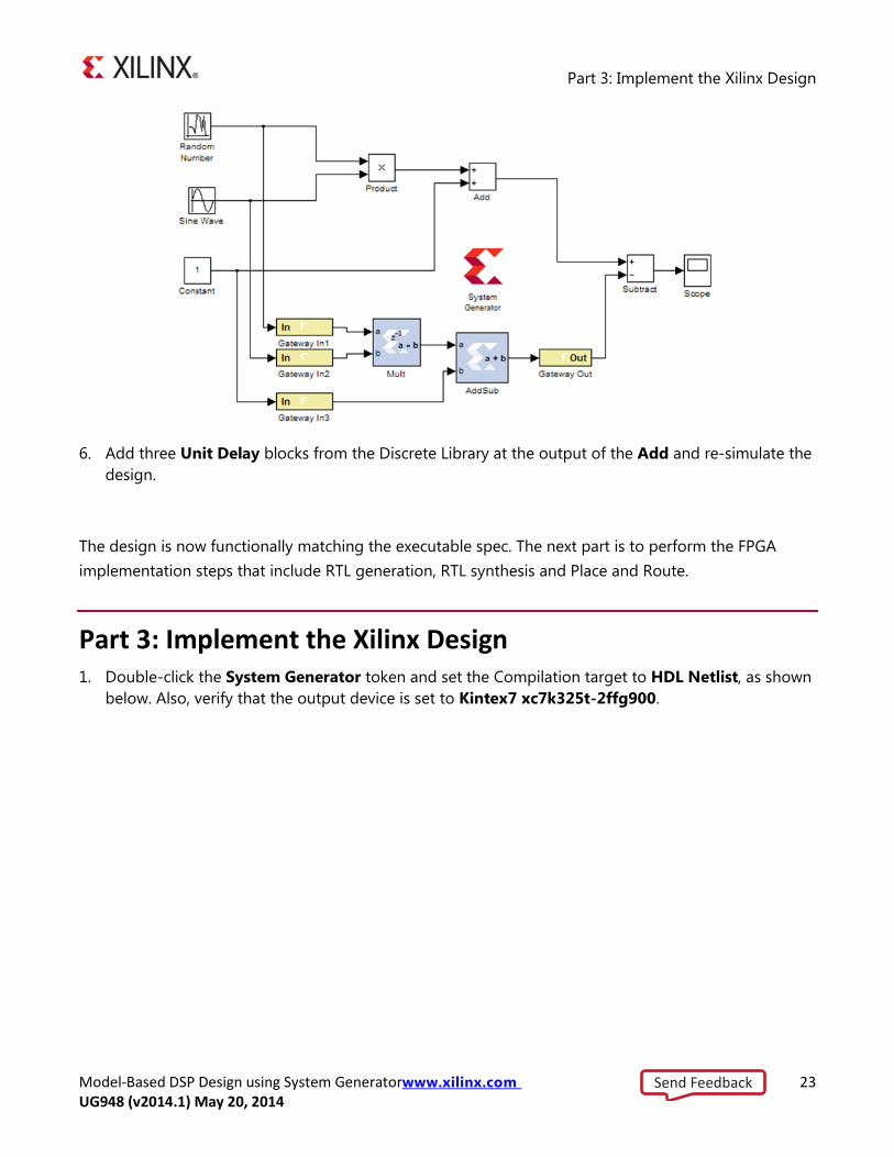
6. Add three Unit Delay blocks from the Discrete Library at the output of the Add and re-simulate the design.
The design is now functionally matching the executable spec. The next part is to perform the FPGA implementation steps that include RTL generation, RTL synthesis and Place and Route.
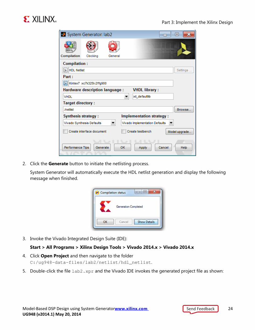
Part 3: Implement the Xilinx Design 1. Double-click the System Generator token and set the Compilation target to HDL Netlist, as shown
below. Also, verify that the output device is set to Kintex7 xc7k325t-2ffg900.
Send Feedback
Part 3: Implement the Xilinx Design
Model-Based DSP Design using System Generatorwww.xilinx.com 24 UG948 (v2014.1) May 20, 2014
2. Click the Generate button to initiate the netlisting process.
System Generator will automatically execute the HDL netlist generation and display the following message when finished.
3. Invoke the Vivado Integrated Design Suite (IDE):
Start > All Programs > Xilinx Design Tools > Vivado 2014.x > Vivado 2014.x
4. Click Open Project and then navigate to the folder C:/ug948-data-files/lab2/netlist/hdl_netlist.
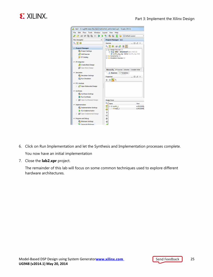
5. Double-click the file lab2.xpr and the Vivado IDE invokes the generated project file as shown:
Send Feedback
Part 3: Implement the Xilinx Design
Model-Based DSP Design using System Generatorwww.xilinx.com 25 UG948 (v2014.1) May 20, 2014
6. Click on Run Implementation and let the Synthesis and Implementation processes complete.
You now have an initial implementation
7. Close the lab2.xpr project.
The remainder of this lab will focus on some common techniques used to explore different hardware architectures.
Send Feedback
Part 4: Explore Different Hardware Architectures
Model-Based DSP Design using System Generatorwww.xilinx.com 26 UG948 (v2014.1) May 20, 2014
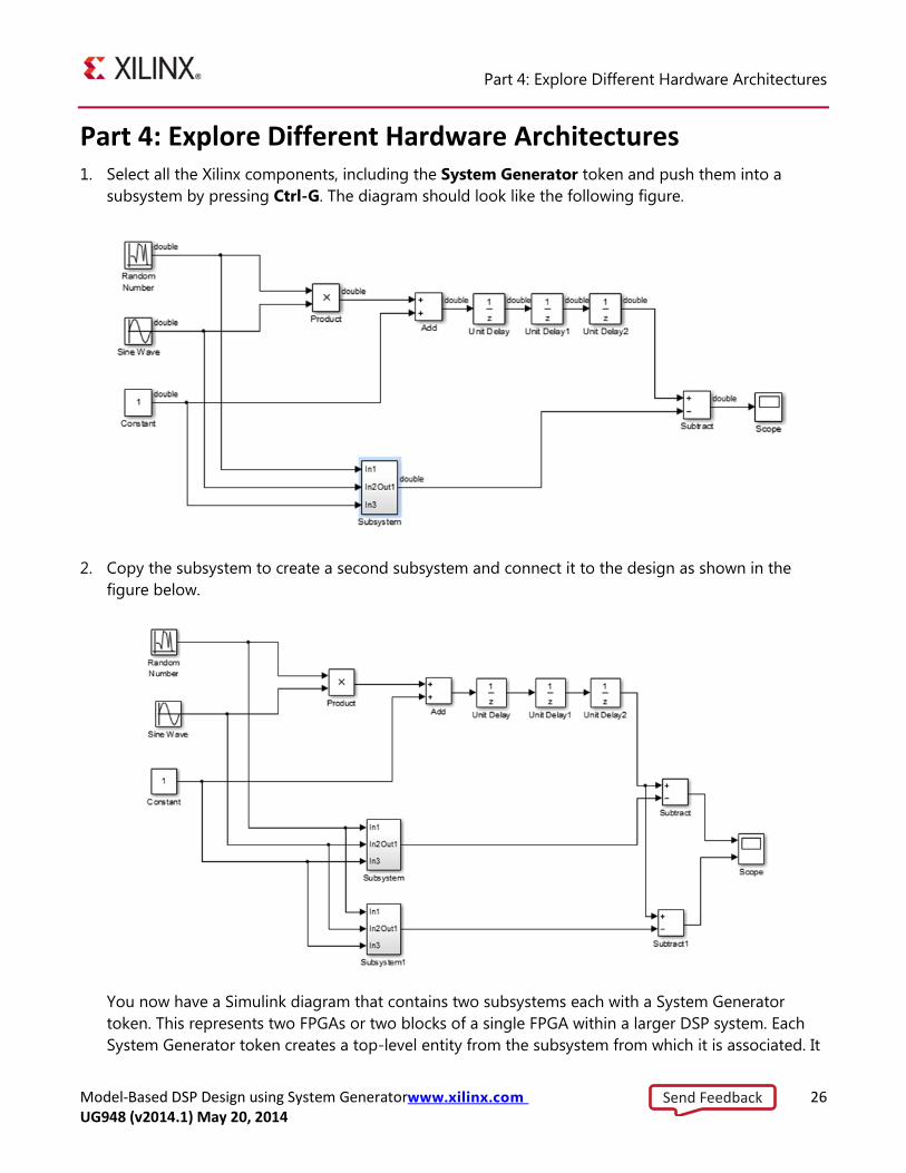
Part 4: Explore Different Hardware Architectures 1. Select all the Xilinx components, including the System Generator token and push them into a
subsystem by pressing Ctrl-G. The diagram should look like the following figure.
2. Copy the subsystem to create a second subsystem and connect it to the design as shown in the figure below.
You now have a Simulink diagram that contains two subsystems each with a System Generator token. This represents two FPGAs or two blocks of a single FPGA within a larger DSP system. Each System Generator token creates a top-level entity from the subsystem from which it is associated. It
Send Feedback
Part 4: Explore Different Hardware Architectures
Model-Based DSP Design using System Generatorwww.xilinx.com 27 UG948 (v2014.1) May 20, 2014
will not merge with the other subsystem. Creating subsystems can be a useful technique when exploring hardware architectures for a given design.
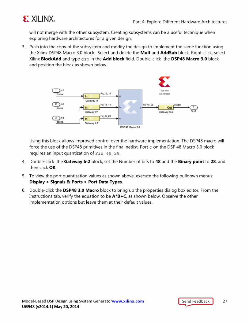
3. Push into the copy of the subsystem and modify the design to implement the same function using the Xilinx DSP48 Macro 3.0 block. Select and delete the Mult and AddSub block. Right-click, select Xilinx BlockAdd and type dsp in the Add block field. Double-click the DSP48 Macro 3.0 block and position the block as shown below.
Using this block allows improved control over the hardware implementation. The DSP48 macro will force the use of the DSP48 primitives in the final netlist. Port c on the DSP 48 Macro 3.0 block requires an input quantization of Fix_48_28.
4. Double-click the Gateway In2 block, set the Number of bits to 48 and the Binary point to 28, and then click OK.
5. To view the port quantization values as shown above, execute the following pulldown menus: Display > Signals & Ports > Port Data Types.
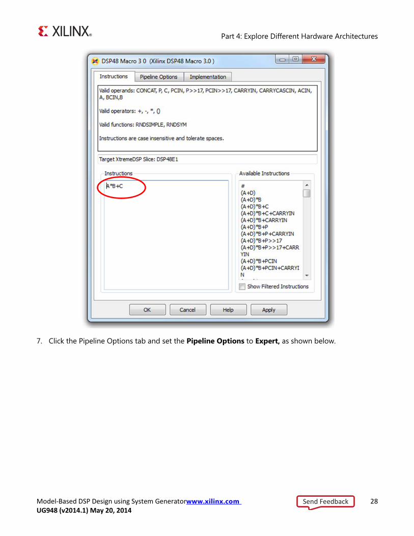
6. Double-click the DSP48 3.0 Macro block to bring up the properties dialog box editor. From the Instructions tab, verify the equation to be A*B+C, as shown below. Observe the other implementation options but leave them at their default values.
Send Feedback
Part 4: Explore Different Hardware Architectures
Model-Based DSP Design using System Generatorwww.xilinx.com 28 UG948 (v2014.1) May 20, 2014
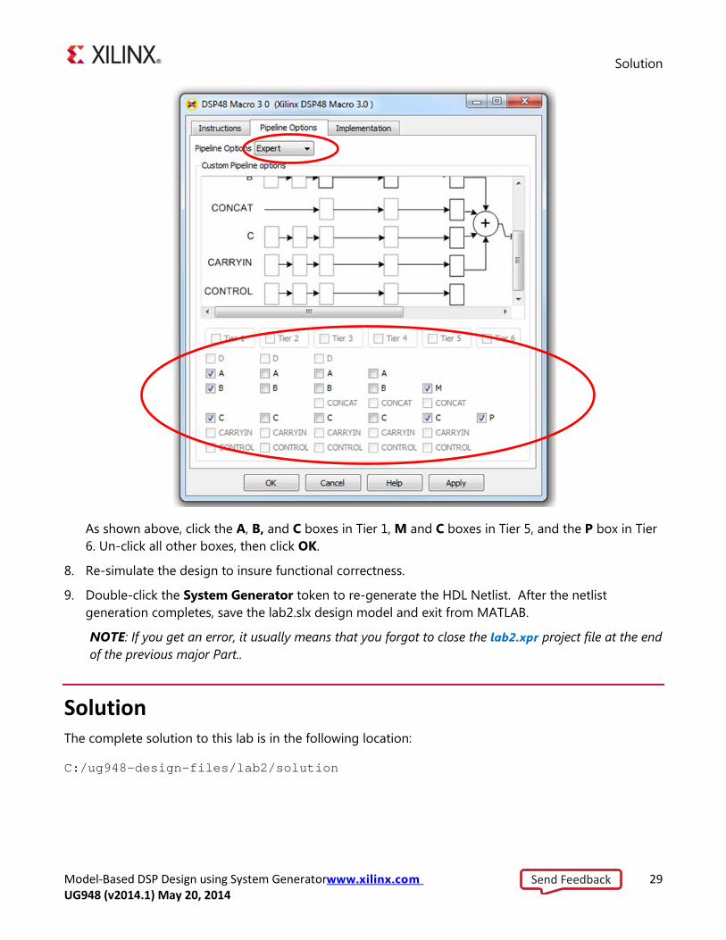
7. Click the Pipeline Options tab and set the Pipeline Options to Expert, as shown below.
Send Feedback
Solution
Model-Based DSP Design using System Generatorwww.xilinx.com 29 UG948 (v2014.1) May 20, 2014
As shown above, click the A, B, and C boxes in Tier 1, M and C boxes in Tier 5, and the P box in Tier 6. Un-click all other boxes, then click OK.
8. Re-simulate the design to insure functional correctness.
9. Double-click the System Generator token to re-generate the HDL Netlist. After the netlist generation completes, save the lab2.slx design model and exit from MATLAB.
NOTE: If you get an error, it usually means that you forgot to close the lab2.xpr project file at the end of the previous major Part..
Solution The complete solution to this lab is in the following location:
C:/ug948-design-files/lab2/solution
Send Feedback
Model-Based DSP Design using System Generatorwww.xilinx.com 30 UG948 (v2014.1) May 20, 2014
Lab 3: Signal Routing
Introduction This lab exercise introduces you to the System Generator features that you will use to convert fixed-point numbers from floating-point, re-define the fixed-point format, as well as perform bit slice, pad and unpad operations. You will also design and verify the padding and unpadding logic using the System Generator signal routing blocks.
Objectives After completing this lab, you will be able to:
• Understand how signal routing blocks can be used to redefine or modify a fixed-point number at the bit level
• Convert a fixed-point number into a new fixed-point number
• Slice bits from a fixed-point number
• Pad and Unpad a fixed-point number
Part 1: Designing Padding Logic 1. Launch the MATLAB program and change the working directory to:
C:/ug948-design-files/lab3
2. Launch the Simulink library browser by clicking on the Simulink icon on the MATLAB toolbar:
3. As shown below, click the New model button in the Simulink Library Browser to create a new model blank sheet.
Send Feedback
Part 1: Designing Padding Logic
Model-Based DSP Design using System Generatorwww.xilinx.com 31 UG948 (v2014.1) May 20, 2014
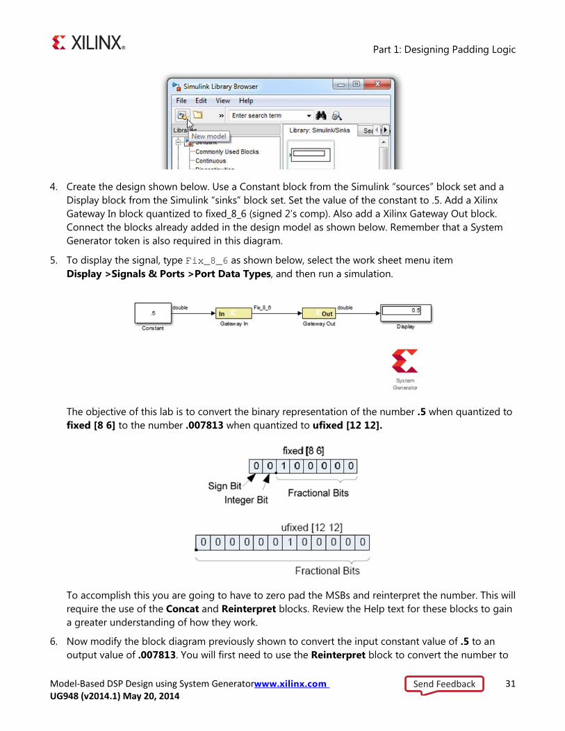
4. Create the design shown below. Use a Constant block from the Simulink “sources” block set and a Display block from the Simulink “sinks” block set. Set the value of the constant to .5. Add a Xilinx Gateway In block quantized to fixed_8_6 (signed 2’s comp). Also add a Xilinx Gateway Out block. Connect the blocks already added in the design model as shown below. Remember that a System Generator token is also required in this diagram.
5. To display the signal, type Fix_8_6 as shown below, select the work sheet menu item Display >Signals & Ports >Port Data Types, and then run a simulation.
The objective of this lab is to convert the binary representation of the number .5 when quantized to fixed [8 6] to the number .007813 when quantized to ufixed [12 12].
To accomplish this you are going to have to zero pad the MSBs and reinterpret the number. This will require the use of the Concat and Reinterpret blocks. Review the Help text for these blocks to gain a greater understanding of how they work.
6. Now modify the block diagram previously shown to convert the input constant value of .5 to an output value of .007813. You will first need to use the Reinterpret block to convert the number to
Send Feedback
Part 2: Designing Unpadding Logic
Model-Based DSP Design using System Generatorwww.xilinx.com 32 UG948 (v2014.1) May 20, 2014
ufix [8 0]. You then use a Constant and Concat block to convert to ufix [12 0], and then use another Reinterpret block to convert ufix [12 12].
The solution to this exercise can be found in the following location: C:/ug948-design-files/lab3/solution/lab3_padding_solution.slx.
Part 2: Designing Unpadding Logic 1. You are going to perform an exercise similar to Part 1, but in the other direction. Here the input will
be the constant .007813 and you want the output to be converted to .5 through bit manipulation, not arithmetic.
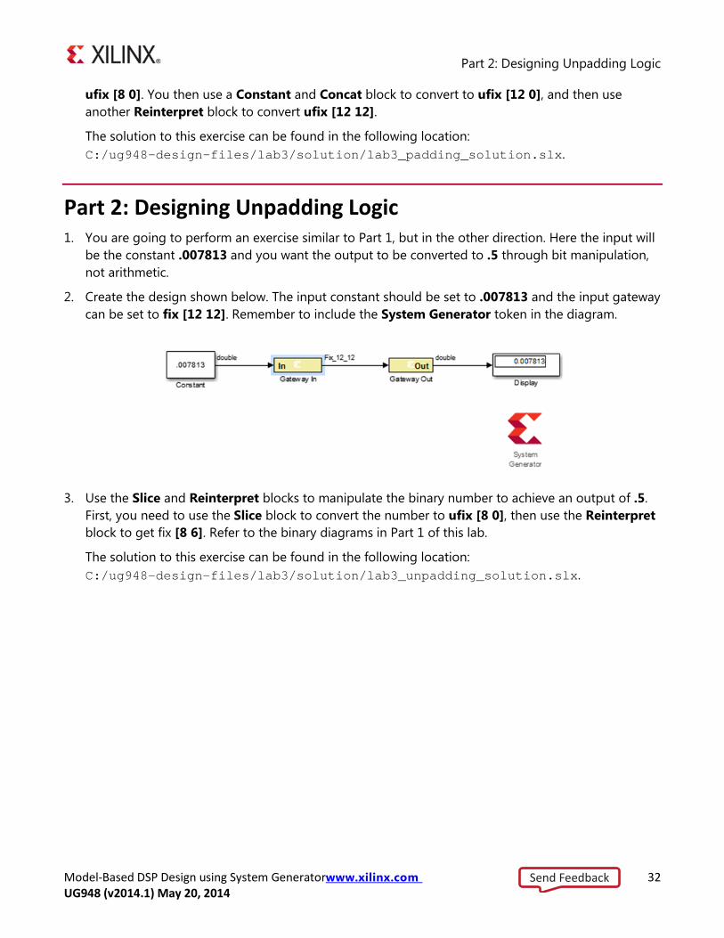
2. Create the design shown below. The input constant should be set to .007813 and the input gateway can be set to fix [12 12]. Remember to include the System Generator token in the diagram.
3. Use the Slice and Reinterpret blocks to manipulate the binary number to achieve an output of .5. First, you need to use the Slice block to convert the number to ufix [8 0], then use the Reinterpret block to get fix [8 6]. Refer to the binary diagrams in Part 1 of this lab.
The solution to this exercise can be found in the following location: C:/ug948-design-files/lab3/solution/lab3_unpadding_solution.slx.
Send Feedback

Solution
Model-Based DSP Design using System Generatorwww.xilinx.com 33 UG948 (v2014.1) May 20, 2014
Solution Solutions to this lab can be found in the following location: C:/ug948-design-files/lab3/solution.
Send Feedback
Model-Based DSP Design using System Generatorwww.xilinx.com 34 UG948 (v2014.1) May 20, 2014
Lab 4: System Control
Introduction In this lab exercise you will be creating a simple finite state machine (FSM) using the MCode block to detect a sequence of binary values 1011. The FSM needs to be able to detect multiple transmissions as well, such as 10111011.
Objectives After completing this lab, you will be able to create a finite state machine using the Mcode block in System Generator
Procedure 1. Launch the MATLAB program and change the working directory to: C:/ug948-design-
files/lab4.
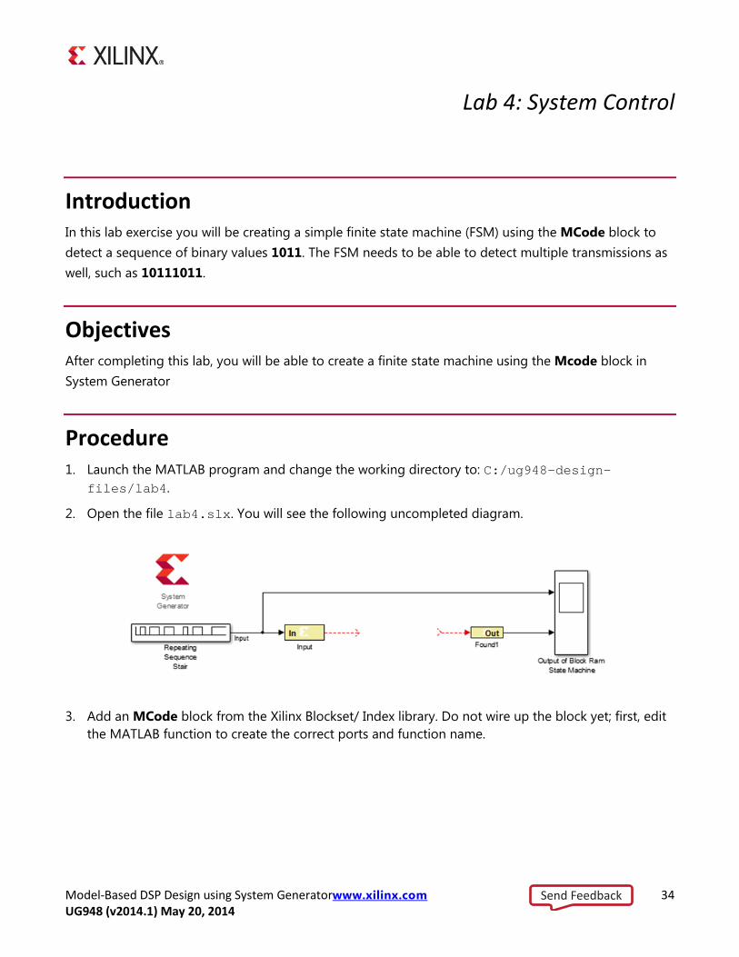
2. Open the file lab4.slx. You will see the following uncompleted diagram.
3. Add an MCode block from the Xilinx Blockset/ Index library. Do not wire up the block yet; first, edit the MATLAB function to create the correct ports and function name.
Send Feedback
Procedure
Model-Based DSP Design using System Generatorwww.xilinx.com 35 UG948 (v2014.1) May 20, 2014
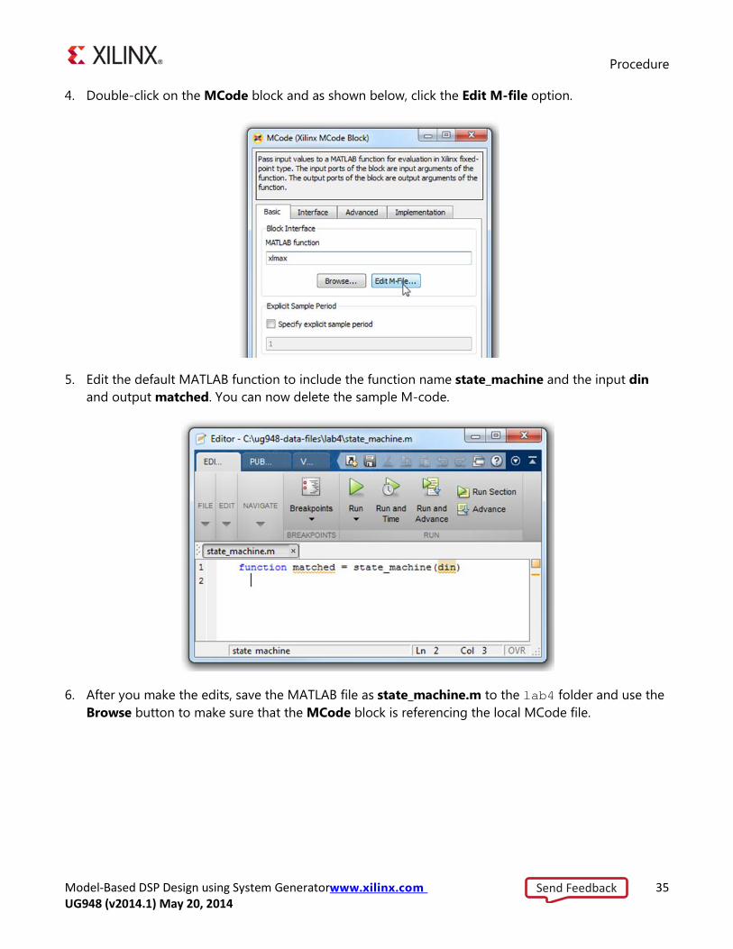
4. Double-click on the MCode block and as shown below, click the Edit M-file option.
5. Edit the default MATLAB function to include the function name state_machine and the input din and output matched. You can now delete the sample M-code.
6. After you make the edits, save the MATLAB file as state_machine.m to the lab4 folder and use the Browse button to make sure that the MCode block is referencing the local MCode file.
Send Feedback
Procedure
Model-Based DSP Design using System Generatorwww.xilinx.com 36 UG948 (v2014.1) May 20, 2014
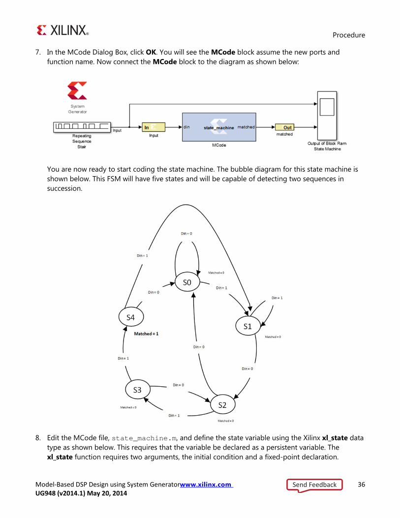
7. In the MCode Dialog Box, click OK. You will see the MCode block assume the new ports and function name. Now connect the MCode block to the diagram as shown below:
You are now ready to start coding the state machine. The bubble diagram for this state machine is shown below. This FSM will have five states and will be capable of detecting two sequences in succession.
8. Edit the MCode file, state_machine.m, and define the state variable using the Xilinx xl_state data type as shown below. This requires that the variable be declared as a persistent variable. The xl_state function requires two arguments, the initial condition and a fixed-point declaration.
Send Feedback
Solution
Model-Based DSP Design using System Generatorwww.xilinx.com 37 UG948 (v2014.1) May 20, 2014
Because you need to count up to 4, you need 3 bits. persistent state, state = xl_state(0,{xlUnsigned, 3, 0});
9. Use a switch-case statement to define the FSM states shown. A small sample is provided below to get you started.
Note: you need an otherwise statement as your last case. switch state case 0 if din == 1 state = 1; else state = 0; end matched = 0;
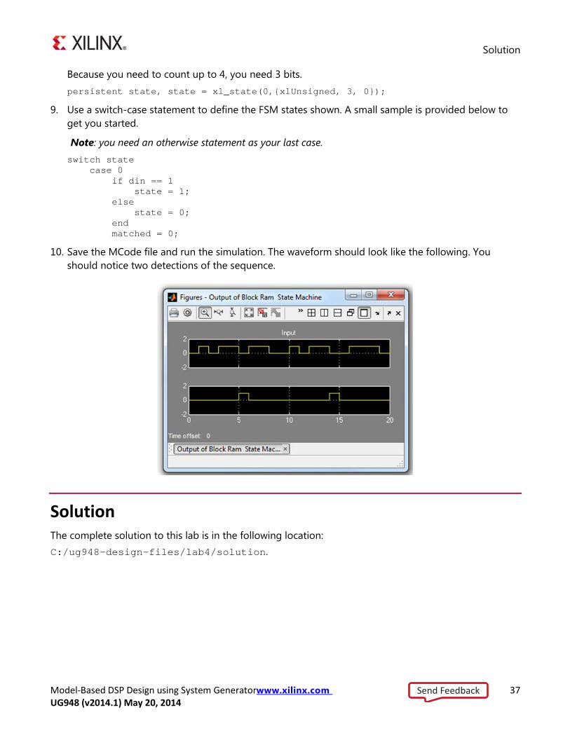
10. Save the MCode file and run the simulation. The waveform should look like the following. You should notice two detections of the sequence.
Solution The complete solution to this lab is in the following location: C:/ug948-design-files/lab4/solution.
Send Feedback
Model-Based DSP Design using System Generatorwww.xilinx.com 38 UG948 (v2014.1) May 20, 2014
Lab 5: Multi-Rate Systems
Lab 5 Introduction In this lab exercise you will explore the effects of the rate changing blocks available in System Generator including the Up Sample, Down Sample, Serial to Parallel and Parallel to Serial blocks.
• Upsampling is the process of increasing the sampling rate of a signal.
• Down sampling is the process of decreasing the sampling rate of a signal. It is common practice in signal processing systems to change the sample rate of a signal to simplify the hardware or processing tasks.
Objectives After completing this lab, you will be able to:
• Change the sample rates in a DSP System
• Convert a serial stream of data to a parallel word
• Convert a parallel word of data into a serial stream
Part 1: Changing Sample Rate 1. Launch the MATLAB program and change the working directory to: C:/ug948-design-
files/lab5.
2. Open a new Simulink model and save it as lab5.slx in the current working directory.
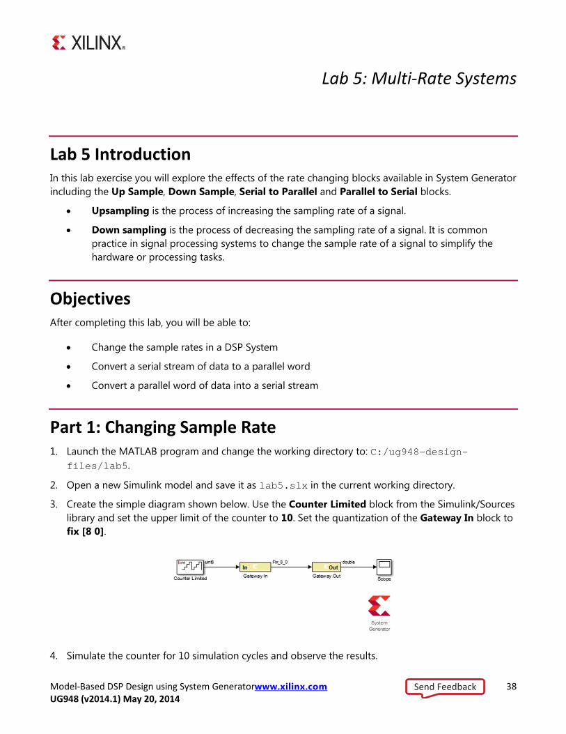
3. Create the simple diagram shown below. Use the Counter Limited block from the Simulink/Sources library and set the upper limit of the counter to 10. Set the quantization of the Gateway In block to fix [8 0].
4. Simulate the counter for 10 simulation cycles and observe the results.
Send Feedback

Part 1: Changing Sample Rate
Model-Based DSP Design using System Generatorwww.xilinx.com 39 UG948 (v2014.1) May 20, 2014
5. As shown below, add a Down Sample block from the Xilinx Blockset/Index library between the Gateway In and Gateway Out blocks, then re-simulate the design.
What do you observe?
___________________________________________________________________________
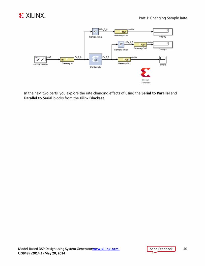
6. Replace the Down Sample block with an Up Sample block and re-simulate the design. The System Generator token is going to generate an error that indicates your sample rate is incorrect.
7. Double-click the System Generator token and change the Simulink System Period to ½ as the message suggests.
8. Re-simulate the design.
9. Add Sample Time probes from the Xilinx Blockset/Index library before and after the Up Sample block and connect the outputs of the probes to Gateway Out blocks and the Display block from the Simulink/Sinks as shown in the following figure.
These probes do not add any hardware to the design, but offer a powerful debugging tool for complex multi-rate systems.
10. Re-simulate the design to observe the sample rate in the Display sinks.
Send Feedback
Part 1: Changing Sample Rate
Model-Based DSP Design using System Generatorwww.xilinx.com 40 UG948 (v2014.1) May 20, 2014
In the next two parts, you explore the rate changing effects of using the Serial to Parallel and Parallel to Serial blocks from the Xilinx Blockset.
Send Feedback
Part 2: Using Serial-to-Parallel Blocks
Model-Based DSP Design using System Generatorwww.xilinx.com 41 UG948 (v2014.1) May 20, 2014
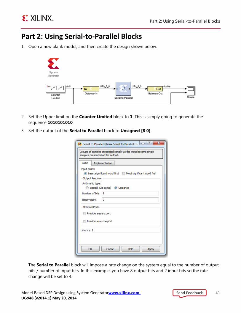
Part 2: Using Serial-to-Parallel Blocks 1. Open a new blank model, and then create the design shown below.
2. Set the Upper limit on the Counter Limited block to 1. This is simply going to generate the sequence 1010101010.
3. Set the output of the Serial to Parallel block to Unsigned [8 0].
The Serial to Parallel block will impose a rate change on the system equal to the number of output bits / number of input bits. In this example, you have 8 output bits and 2 input bits so the rate change will be set to 4.
Send Feedback
Part 3: Using Parallel-to-Serial Blocks
Model-Based DSP Design using System Generatorwww.xilinx.com 42 UG948 (v2014.1) May 20, 2014
4. In the Block dialog box, click OK, and then add sample rate probes to the input and output of the Serial to Parallel block. Re-simulate the design and observe the sample rates.
Input Sample Rate __________
Output Sample Rate __________
5. Change the output quantization of the Serial to Parallel block to fix [16 0] and re-simulate. What are the sample rates now?
Input Sample Rate __________
Output Sample Rate __________
Part 3: Using Parallel-to-Serial Blocks 1. Replace the Serial to Parallel block with the Parallel to Serial block. Leave the output quantization
at the default ufix [1 0].
2. Change the sample rate in the System Generator token from 1 to ½, then click OK.
3. Re-simulate the design and record the input and output sample rates.
Input Sample Rate __________
Output Sample Rate __________
Solution The complete solution to this lab is in the following location: C:/ug948-design-files/lab5/solution.
Send Feedback
Model-Based DSP Design using System Generatorwww.xilinx.com 43 UG948 (v2014.1) May 20, 2014
Lab 6: Using Memories
Lab 6 Introduction In this lab exercise you will learn how to use a Xilinx ROM block to implement a LUT-based operation such as an arcsin using block or distributed RAM. This provides an efficient implementation for trig and math functions with inputs that can be quantized to 10 bits or less.
Objectives After completing this lab, you will be able to use a Xilinx ROM block to implement a trig or math function such as arcsin.
Procedure 1. Launch the MATLAB program and change the working directory to:
C:/ug948-design-files/lab6.
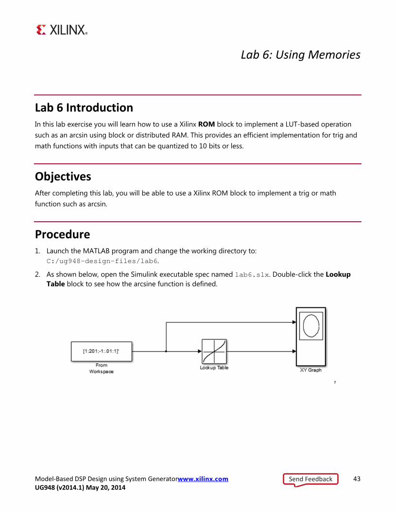
2. As shown below, open the Simulink executable spec named lab6.slx. Double-click the Lookup Table block to see how the arcsine function is defined.
Send Feedback
Procedure
Model-Based DSP Design using System Generatorwww.xilinx.com 44 UG948 (v2014.1) May 20, 2014
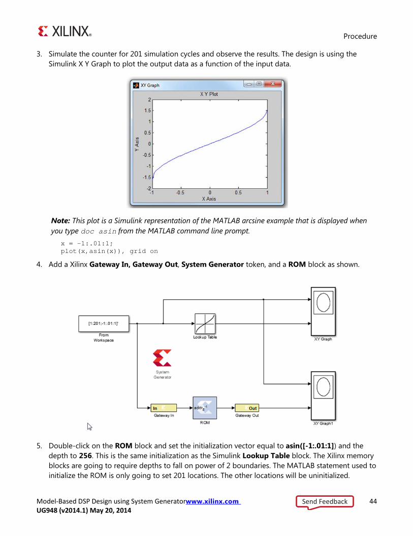
3. Simulate the counter for 201 simulation cycles and observe the results. The design is using the Simulink X Y Graph to plot the output data as a function of the input data.
Note: This plot is a Simulink representation of the MATLAB arcsine example that is displayed when you type doc asin from the MATLAB command line prompt. x = -1:.01:1; plot(x,asin(x)), grid on
4. Add a Xilinx Gateway In, Gateway Out, System Generator token, and a ROM block as shown.
5. Double-click on the ROM block and set the initialization vector equal to asin([-1:.01:1]) and the depth to 256. This is the same initialization as the Simulink Lookup Table block. The Xilinx memory blocks are going to require depths to fall on power of 2 boundaries. The MATLAB statement used to initialize the ROM is only going to set 201 locations. The other locations will be uninitialized.
Send Feedback
Procedure
Model-Based DSP Design using System Generatorwww.xilinx.com 45 UG948 (v2014.1) May 20, 2014
6. Simulate the design for 201 clock cycles. You are going to get an error indicating an incorrect quantization at the input of the ROM block. You left the quantization of the Gateway In block to the default value of fixed [16 14]. To address a Xilinx memory, the quantization must be ufix with no fractional bits. Because you have a 256 element address space, you are going to need an input quantization of ufix [8 0].
7. Change the gateway and re-simulate.
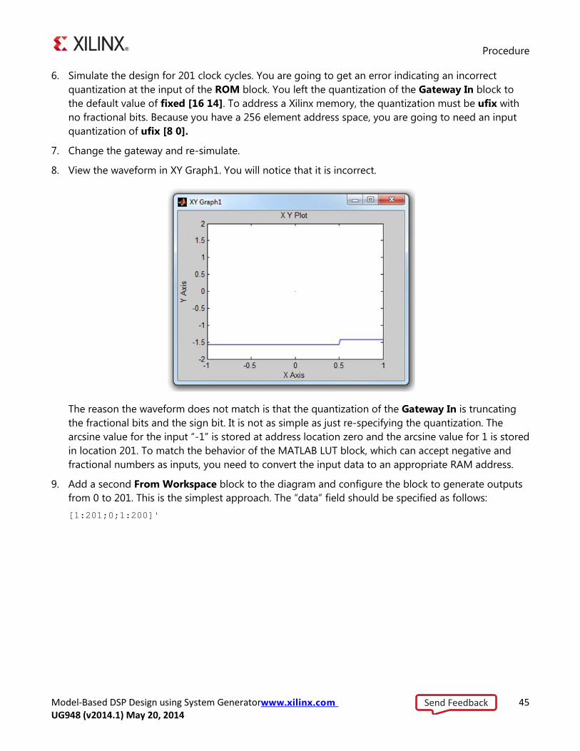
8. View the waveform in XY Graph1. You will notice that it is incorrect.
The reason the waveform does not match is that the quantization of the Gateway In is truncating the fractional bits and the sign bit. It is not as simple as just re-specifying the quantization. The arcsine value for the input “-1” is stored at address location zero and the arcsine value for 1 is stored in location 201. To match the behavior of the MATLAB LUT block, which can accept negative and fractional numbers as inputs, you need to convert the input data to an appropriate RAM address.
9. Add a second From Workspace block to the diagram and configure the block to generate outputs from 0 to 201. This is the simplest approach. The “data” field should be specified as follows: [1:201;0;1:200]'
Send Feedback

Solution
Model-Based DSP Design using System Generatorwww.xilinx.com 46 UG948 (v2014.1) May 20, 2014
10. Re-simulate. You should see correct results.
11. Because System Generator does not generate a Bitstream, you need to generate an HDL Netlist, then open the project file in the Vivado IDE and generate a Bitstream.
12. Record the results.
Registers ________________
Block RAMs ________________
Slices ________________
13. Double-click the ROM block and set the Memory Type field to Distributed. Run System Generator and record the results.
Registers ________________
Block RAMs ________________
Slices ________________
Solution The complete solution to this lab is in the following location: C:/ug948-design-files/lab6/solution.
Send Feedback
Lab 7 Introduction
Model-Based DSP Design using System Generatorwww.xilinx.com 47 UG948 (v2014.1) May 20, 2014
Lab 7: Including a System Generator Model in a Vivado IDE Design
Lab 7 Introduction Typically, a System Design Engineer has to include hardware design sources from a variety of different formats and put them together into a final system-level design. This lab exercise provides an overview of how you can include a System Generator model within a Vivado® IDE design and combine that model with other RTL sources.
Part 1: Create a new Vivado IDE Project and add RTL/DSP sources and XDC constraints 1. Invoke the Vivado Integrated Design Suite (IDE): Start > All Programs > Xilinx Design Tools >
Vivado 2014.x > Vivado 2014.x
2. Select the pull-down menu File > New Project and then click Next .
Send Feedback
Part 1: Create a new Vivado IDE Project and add RTL/DSP sources and XDC constraints
Model-Based DSP Design using System Generatorwww.xilinx.com 48 UG948 (v2014.1) May 20, 2014
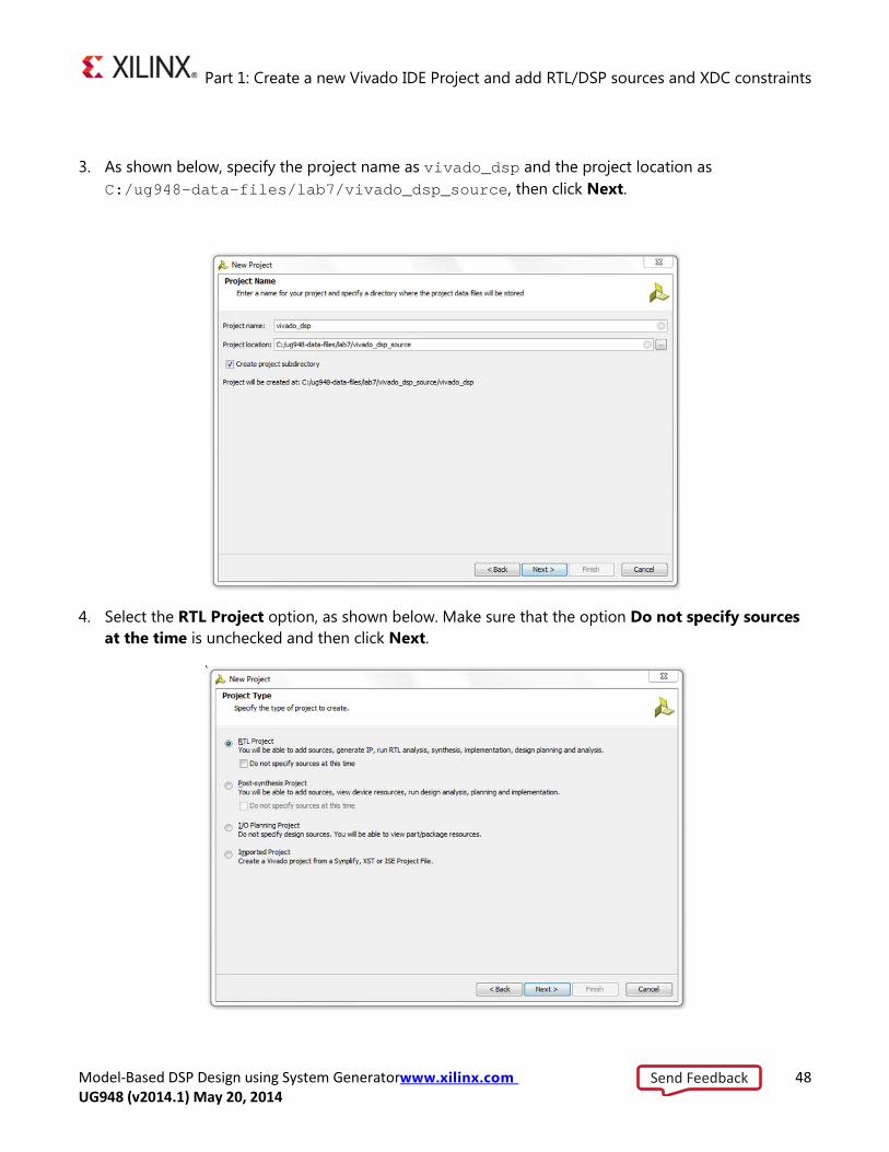
3. As shown below, specify the project name as vivado_dsp and the project location as C:/ug948-data-files/lab7/vivado_dsp_source, then click Next.
4. Select the RTL Project option, as shown below. Make sure that the option Do not specify sources at the time is unchecked and then click Next.
Send Feedback
Part 1: Create a new Vivado IDE Project and add RTL/DSP sources and XDC constraints
Model-Based DSP Design using System Generatorwww.xilinx.com 49 UG948 (v2014.1) May 20, 2014
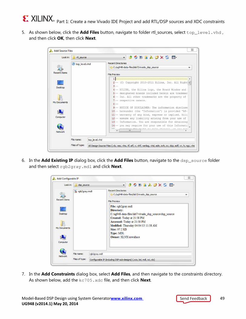
5. As shown below, click the Add Files button, navigate to folder rtl_sources, select top_level.vhd , and then click OK, then click Next.
6. In the Add Existing IP dialog box, click the Add Files button, navigate to the dsp_source folder and then select rgb2gray.mdl and click Next.
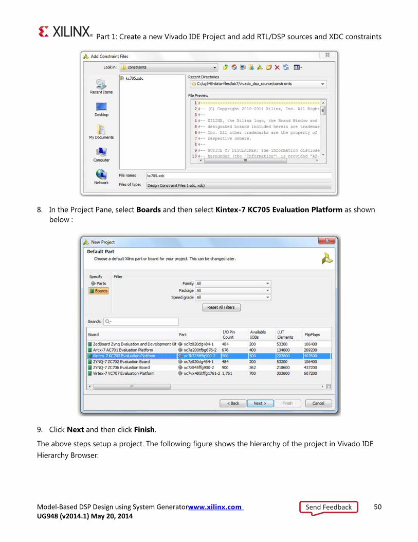
7. In the Add Constraints dialog box, select Add Files, and then navigate to the constraints directory. As shown below, add the kc705.xdc file, and then click Next.
Send Feedback
Part 1: Create a new Vivado IDE Project and add RTL/DSP sources and XDC constraints
Model-Based DSP Design using System Generatorwww.xilinx.com 50 UG948 (v2014.1) May 20, 2014
8. In the Project Pane, select Boards and then select Kintex-7 KC705 Evaluation Platform as shown below :
9. Click Next and then click Finish.
The above steps setup a project. The following figure shows the hierarchy of the project in Vivado IDE Hierarchy Browser:
Send Feedback

Part 1: Create a new Vivado IDE Project and add RTL/DSP sources and XDC constraints
Model-Based DSP Design using System Generatorwww.xilinx.com 51 UG948 (v2014.1) May 20, 2014
Send Feedback
Part 2: Interacting with the DSP Module from the Vivado IDE Cockpit
Model-Based DSP Design using System Generatorwww.xilinx.com 52 UG948 (v2014.1) May 20, 2014
Part 2: Interacting with the DSP Module from the Vivado IDE Cockpit
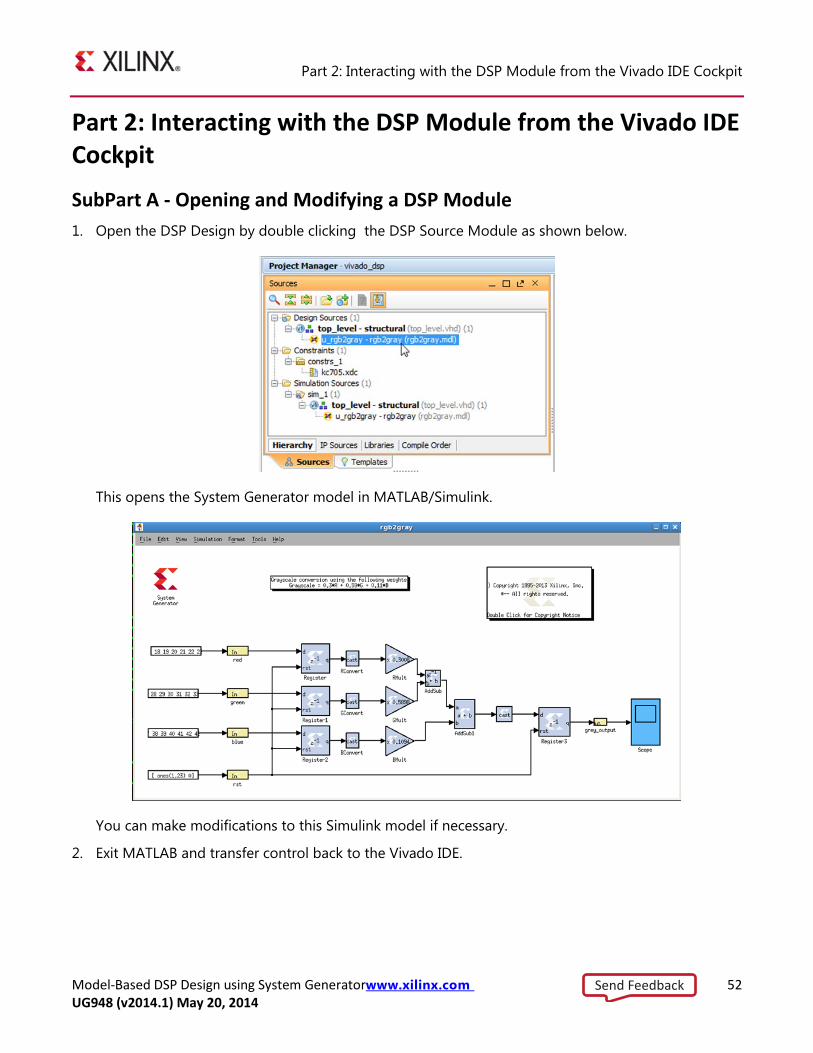
SubPart A - Opening and Modifying a DSP Module 1. Open the DSP Design by double clicking the DSP Source Module as shown below.
This opens the System Generator model in MATLAB/Simulink.
You can make modifications to this Simulink model if necessary.
2. Exit MATLAB and transfer control back to the Vivado IDE.
Send Feedback
Part 2: Interacting with the DSP Module from the Vivado IDE Cockpit
Model-Based DSP Design using System Generatorwww.xilinx.com 53 UG948 (v2014.1) May 20, 2014
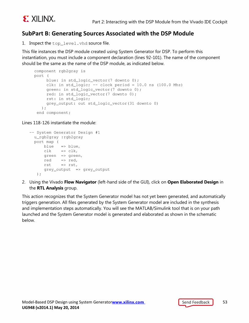
SubPart B: Generating Sources Associated with the DSP Module 1. Inspect the top_level.vhd source file.
This file instances the DSP module created using System Generator for DSP. To perform this instantiation, you must include a component declaration (lines 92-101). The name of the component should be the same as the name of the DSP module, as indicated below.
component rgb2gray is port ( blue: in std_logic_vector(7 downto 0); clk: in std_logic; -- clock period = 10.0 ns (100.0 Mhz) green: in std_logic_vector(7 downto 0); red: in std_logic_vector(7 downto 0); rst: in std_logic; grey_output: out std_logic_vector(31 downto 0) ); end component;
Lines 118-126 instantiate the module: -- System Generator Design #1 u_rgb2gray :rgb2gray port map ( blue => blue, clk => clk, green => green, red => red, rst => rst, grey_output => grey_output );
2. Using the Vivado Flow Navigator (left-hand side of the GUI), click on Open Elaborated Design in the RTL Analysis group.
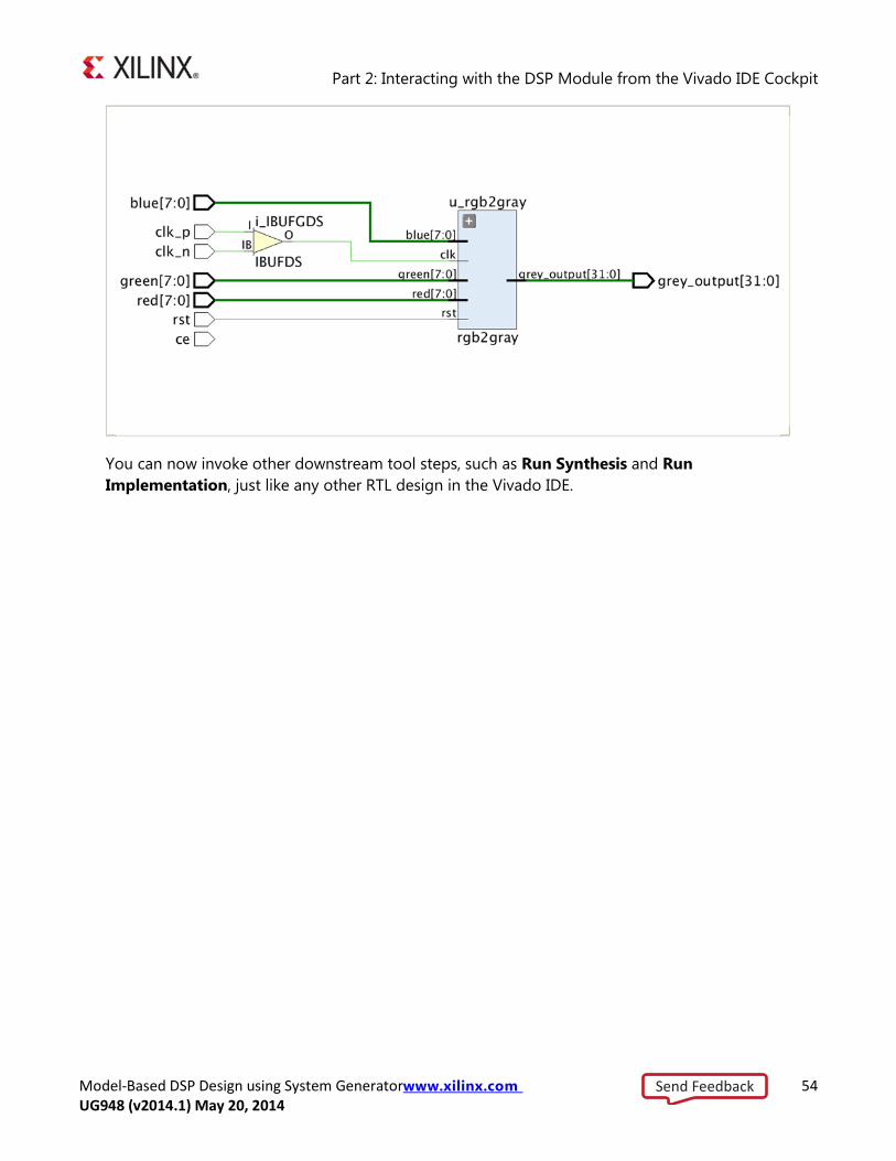
This action recognizes that the System Generator model has not yet been generated, and automatically triggers generation. All files generated by the System Generator model are included in the synthesis and implementation steps automatically. You will see the MATLAB/Simulink tool that is on your path launched and the System Generator model is generated and elaborated as shown in the schematic below.
Send Feedback
Part 2: Interacting with the DSP Module from the Vivado IDE Cockpit
Model-Based DSP Design using System Generatorwww.xilinx.com 54 UG948 (v2014.1) May 20, 2014
You can now invoke other downstream tool steps, such as Run Synthesis and Run Implementation, just like any other RTL design in the Vivado IDE.
Send Feedback

Model-Based DSP Design using System Generatorwww.xilinx.com 55 UG948 (v2014.1) May 20, 2014
Lab 8: Importing C/C++ Source Files into System Generator by Leveraging
Integration with Vivado HLS
Lab 8 Introduction The System Edition of the Vivado® Design Suite, includes the feature called Vivado HLS which has the ability to transform C/C++ design sources into RTL. System Generator has a block called Vivado HLS located in the Control and Index libraries that enables bringing in C/C++ source files into a System Generator model.
Part 1: Creating a System Generator Package from Vivado HLS 1. Invoke Vivado HLS: Start > All Programs > Xilinx Design Tools > Vivado 2014.x > Vivado HLS >
Vivado HLS 2014.x
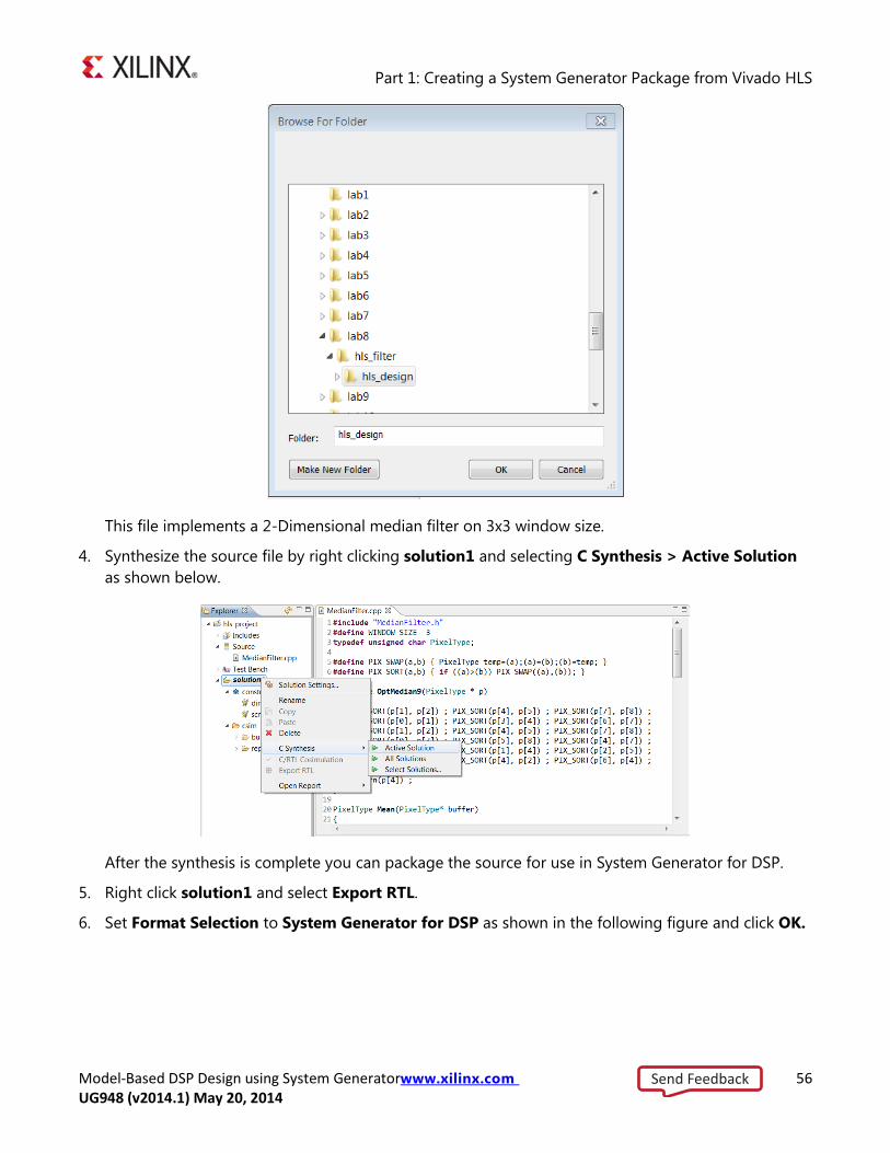
2. Open the Lab8 project hls_project using File > Open Project as shown in the figure below:
3. Inspect the contents of the MedianFilter.cpp file located underneath the sources folder as shown in the following figure.
Send Feedback
Part 1: Creating a System Generator Package from Vivado HLS
Model-Based DSP Design using System Generatorwww.xilinx.com 56 UG948 (v2014.1) May 20, 2014
This file implements a 2-Dimensional median filter on 3x3 window size.
4. Synthesize the source file by right clicking solution1 and selecting C Synthesis > Active Solution as shown below.
After the synthesis is complete you can package the source for use in System Generator for DSP.
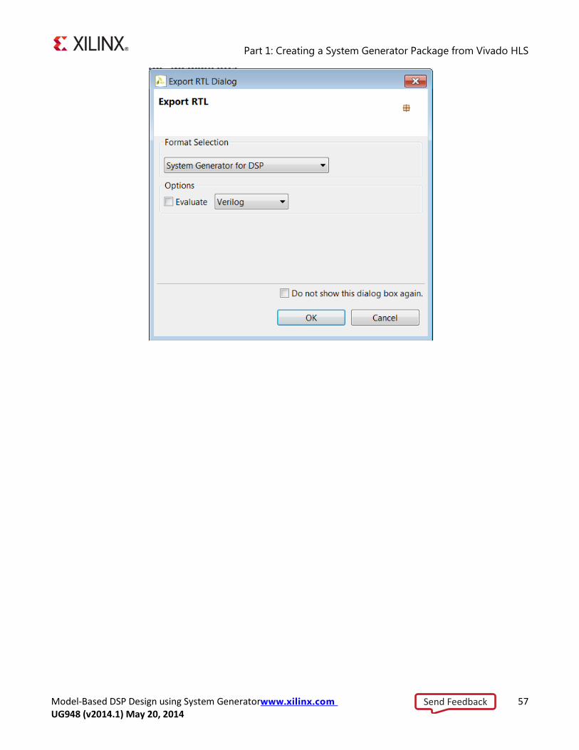
5. Right click solution1 and select Export RTL.
6. Set Format Selection to System Generator for DSP as shown in the following figure and click OK.
Send Feedback
Part 1: Creating a System Generator Package from Vivado HLS
Model-Based DSP Design using System Generatorwww.xilinx.com 57 UG948 (v2014.1) May 20, 2014
Send Feedback
Part 2: Including a Vivado HLS Package in a System Generator Design
Model-Based DSP Design using System Generatorwww.xilinx.com 58 UG948 (v2014.1) May 20, 2014
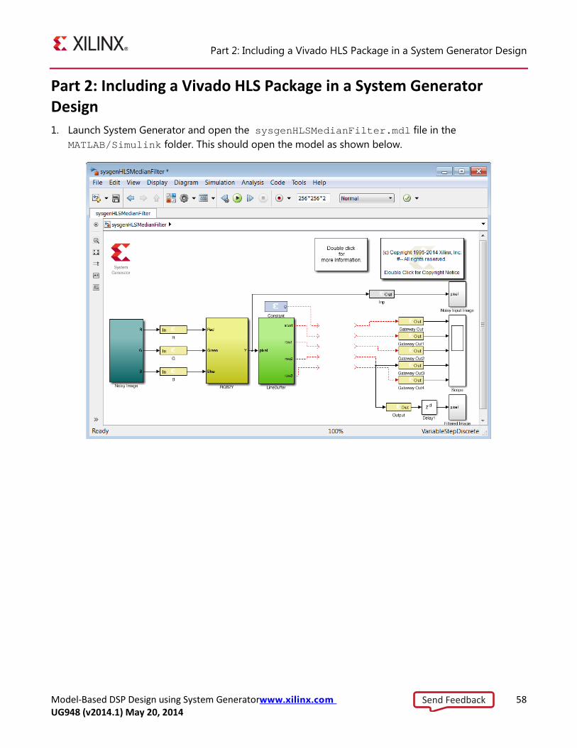
Part 2: Including a Vivado HLS Package in a System Generator Design 1. Launch System Generator and open the sysgenHLSMedianFilter.mdl file in the
MATLAB/Simulink folder. This should open the model as shown below.
Send Feedback

Part 2: Including a Vivado HLS Package in a System Generator Design
Model-Based DSP Design using System Generatorwww.xilinx.com 59 UG948 (v2014.1) May 20, 2014
2. Add a Vivado HLS block by right clicking anywhere on the canvas workspace.
3. Select Xilinx BlockAdd and scroll down to the Vivado HLS block as shown in the figure below.
This adds a block to the model called Vivado HLS as shown in the figure below.
4. Double click the block and use the Browse button to select the solution created by Vivado HLS located underneath the hls_design directory as shown in the following figure.
Send Feedback
Part 2: Including a Vivado HLS Package in a System Generator Design
Model-Based DSP Design using System Generatorwww.xilinx.com 60 UG948 (v2014.1) May 20, 2014
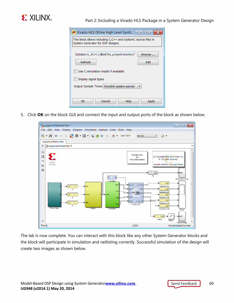
5. Click OK on the block GUI and connect the input and output ports of the block as shown below.
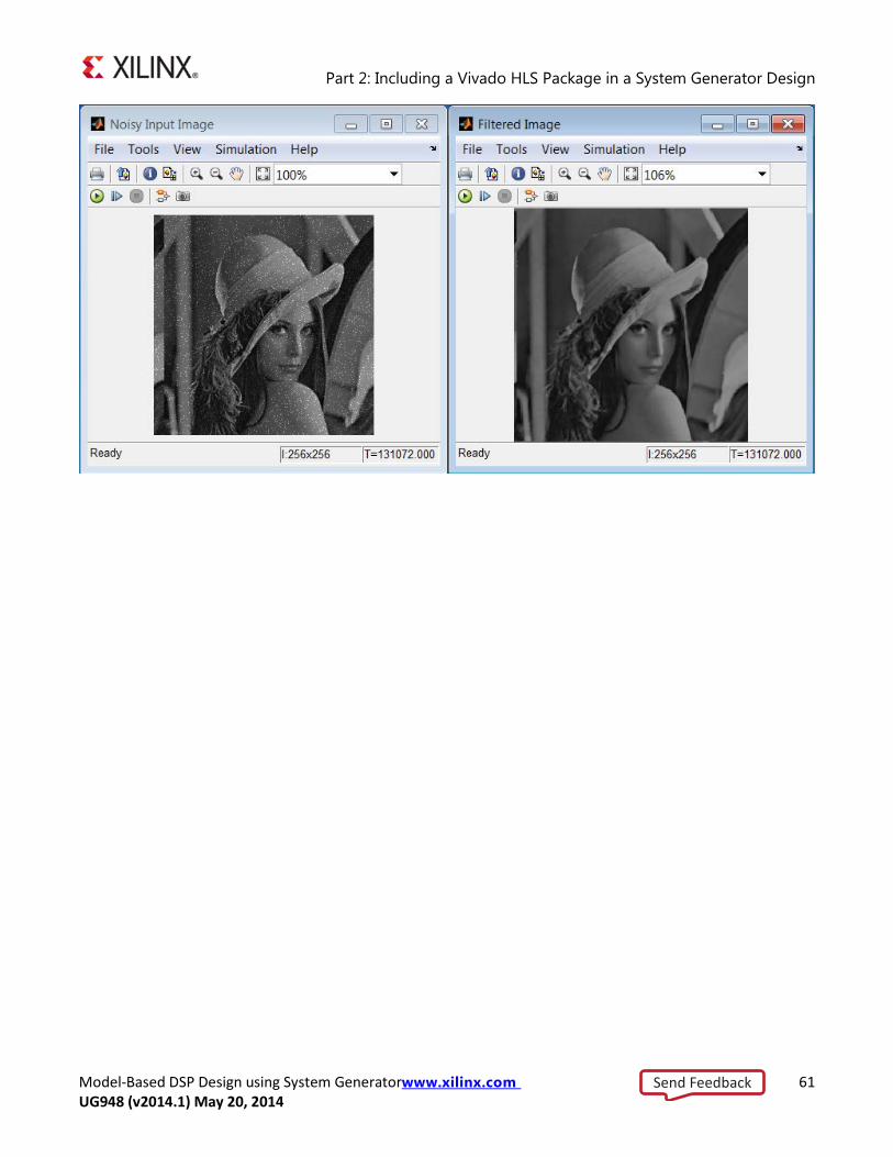
The lab is now complete. You can interact with this block like any other System Generator blocks and the block will participate in simulation and netlisting correctly. Successful simulation of the design will create two images as shown below.
Send Feedback
Part 2: Including a Vivado HLS Package in a System Generator Design
Model-Based DSP Design using System Generatorwww.xilinx.com 61 UG948 (v2014.1) May 20, 2014
Send Feedback
Model-Based DSP Design using System Generatorwww.xilinx.com 62 UG948 (v2014.1) May 20, 2014
Lab 9: Including a System Generator Design as a Module in
an IP Integrator Design
Lab 9 Introduction System Generator has a feature lets you export a design as an IP module into the Vivado® IP Catalog. From the IP Catalog, you can then import the System Generator design as IP into a Vivado IP integrator design. For example, you can create a data-path module in System Generator and then add the data-path to a larger processor-centric design in IP integrator.
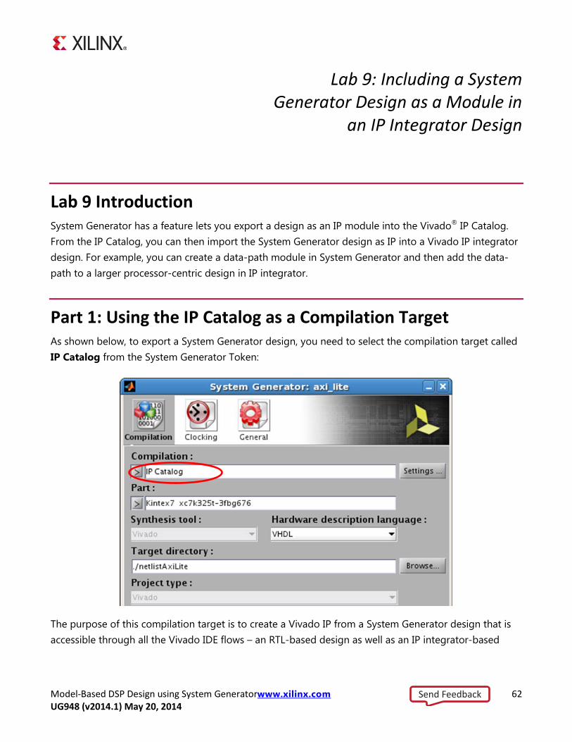
Part 1: Using the IP Catalog as a Compilation Target As shown below, to export a System Generator design, you need to select the compilation target called IP Catalog from the System Generator Token:
The purpose of this compilation target is to create a Vivado IP from a System Generator design that is accessible through all the Vivado IDE flows – an RTL-based design as well as an IP integrator-based
Send Feedback
Part 1: Using the IP Catalog as a Compilation Target
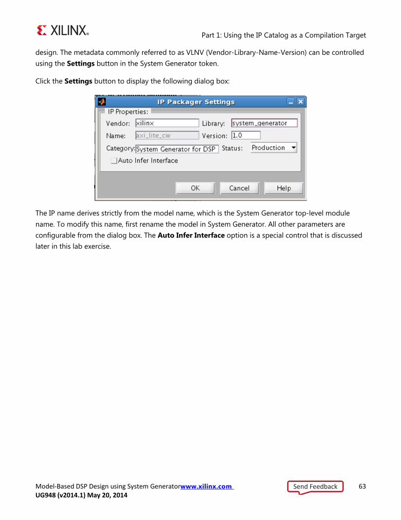
Model-Based DSP Design using System Generatorwww.xilinx.com 63 UG948 (v2014.1) May 20, 2014
design. The metadata commonly referred to as VLNV (Vendor-Library-Name-Version) can be controlled using the Settings button in the System Generator token.
Click the Settings button to display the following dialog box:
The IP name derives strictly from the model name, which is the System Generator top-level module name. To modify this name, first rename the model in System Generator. All other parameters are configurable from the dialog box. The Auto Infer Interface option is a special control that is discussed later in this lab exercise.
Send Feedback
Part 2: Generating Output Products
Model-Based DSP Design using System Generatorwww.xilinx.com 64 UG948 (v2014.1) May 20, 2014
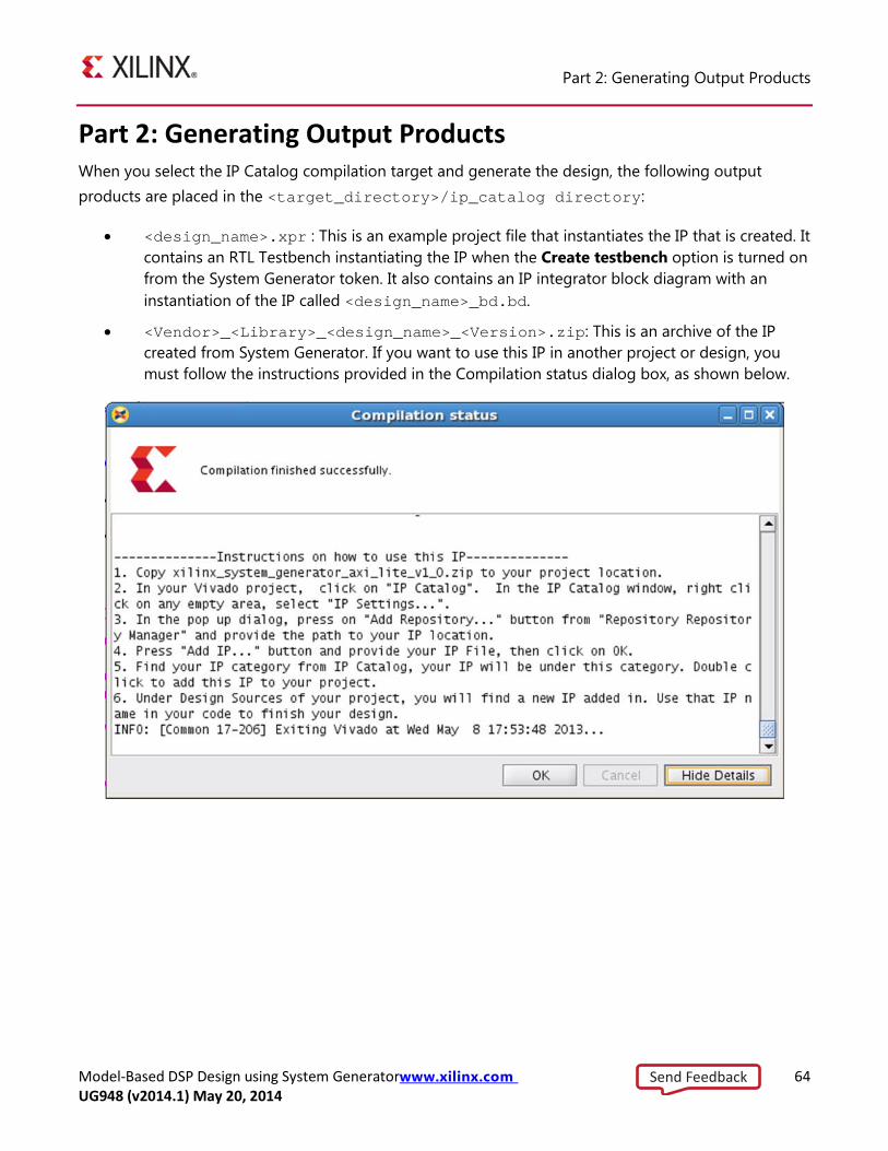
Part 2: Generating Output Products When you select the IP Catalog compilation target and generate the design, the following output products are placed in the <target_directory>/ip_catalog directory:
• <design_name>.xpr : This is an example project file that instantiates the IP that is created. It contains an RTL Testbench instantiating the IP when the Create testbench option is turned on from the System Generator token. It also contains an IP integrator block diagram with an instantiation of the IP called <design_name>_bd.bd.
• <Vendor>_<Library>_<design_name>_<Version>.zip: This is an archive of the IP created from System Generator. If you want to use this IP in another project or design, you must follow the instructions provided in the Compilation status dialog box, as shown below.
Send Feedback
Part 3: IP Creation Modes
Model-Based DSP Design using System Generatorwww.xilinx.com 65 UG948 (v2014.1) May 20, 2014
Part 3: IP Creation Modes There are two IP creation modes in System Generator and a combination of these modes is supported as well.
• Port/Pin Interface Packaging
• Port-Name-Based Interface Inference
Part 4: Port/Pin Interface Packaging In this mode, the Gateway In and Gateway Out blocks are packaged as simple RTL ports.
Do the following:
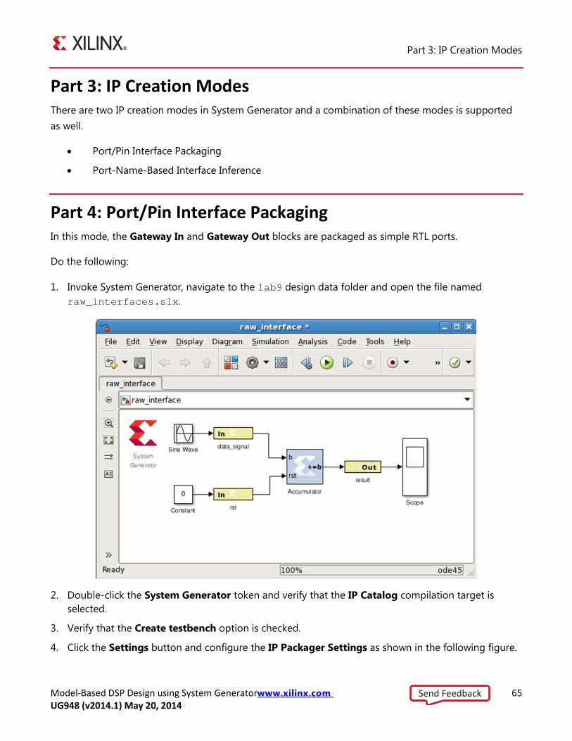
1. Invoke System Generator, navigate to the lab9 design data folder and open the file named raw_interfaces.slx.
2. Double-click the System Generator token and verify that the IP Catalog compilation target is selected.
3. Verify that the Create testbench option is checked.
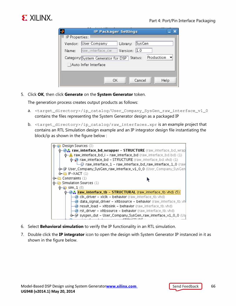
4. Click the Settings button and configure the IP Packager Settings as shown in the following figure.
Send Feedback
Part 4: Port/Pin Interface Packaging
Model-Based DSP Design using System Generatorwww.xilinx.com 66 UG948 (v2014.1) May 20, 2014
5. Click OK, then click Generate on the System Generator token.
The generation process creates output products as follows:
a. <target_directory>/ip_catalog/User_Company_SysGen_raw_interface_v1_0 contains the files representing the System Generator design as a packaged IP
b. <target_directory>/ip_catalog/raw_interfaces.xpr is an example project that contains an RTL Simulation design example and an IP integrator design file instantiating the block/ip as shown in the figure below :
6. Select Behavioral simulation to verify the IP functionality in an RTL simulation.
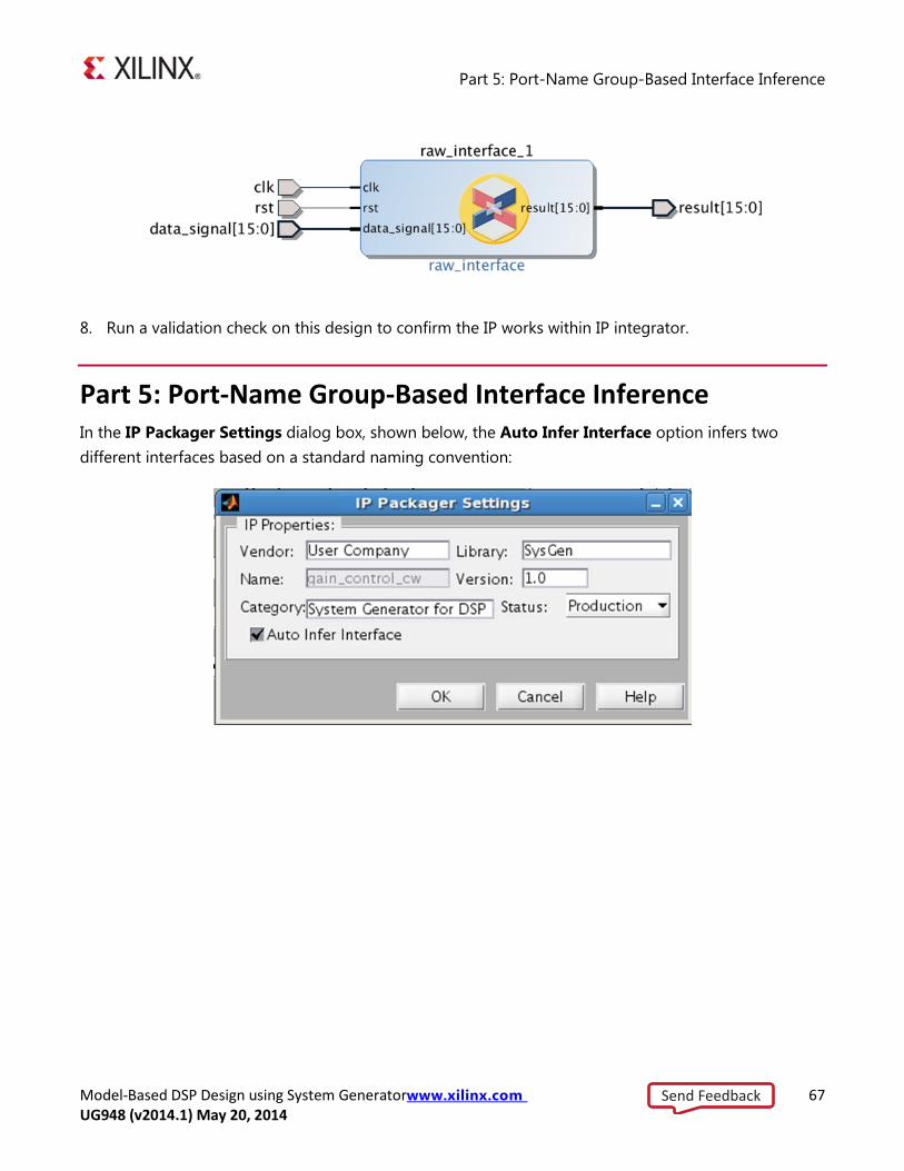
7. Double click the IP integrator icon to open the design with System Generator IP instanced in it as shown in the figure below.
Send Feedback
Part 5: Port-Name Group-Based Interface Inference
Model-Based DSP Design using System Generatorwww.xilinx.com 67 UG948 (v2014.1) May 20, 2014
8. Run a validation check on this design to confirm the IP works within IP integrator.
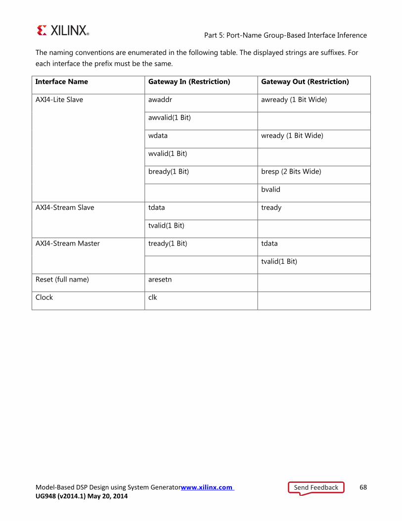
Part 5: Port-Name Group-Based Interface Inference In the IP Packager Settings dialog box, shown below, the Auto Infer Interface option infers two different interfaces based on a standard naming convention:
Send Feedback
Part 5: Port-Name Group-Based Interface Inference
Model-Based DSP Design using System Generatorwww.xilinx.com 68 UG948 (v2014.1) May 20, 2014
The naming conventions are enumerated in the following table. The displayed strings are suffixes. For each interface the prefix must be the same.
Interface Name Gateway In (Restriction) Gateway Out (Restriction)
AXI4-Lite Slave awaddr awready (1 Bit Wide)
awvalid(1 Bit)
wdata wready (1 Bit Wide)
wvalid(1 Bit)
bready(1 Bit) bresp (2 Bits Wide)
bvalid
AXI4-Stream Slave tdata tready
tvalid(1 Bit)
AXI4-Stream Master tready(1 Bit) tdata
tvalid(1 Bit)
Reset (full name) aresetn
Clock clk
Send Feedback

Part 6: Compiling the gain_control Design
Model-Based DSP Design using System Generatorwww.xilinx.com 69 UG948 (v2014.1) May 20, 2014
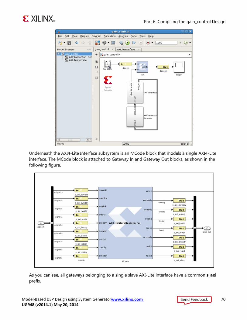
Part 6: Compiling the gain_control Design 1. Navigate to the lab9 folder and open the System Generator design named gain_control.slx.
A gain block is implemented using a multiplier with one input controlled using an AXI4-Lite interface and the other input is part of the data path as shown in the figure below.
Send Feedback
Part 6: Compiling the gain_control Design
Model-Based DSP Design using System Generatorwww.xilinx.com 70 UG948 (v2014.1) May 20, 2014
Underneath the AXI4-Lite Interface subsystem is an MCode block that models a single AXI4-Lite Interface. The MCode block is attached to Gateway In and Gateway Out blocks, as shown in the following figure.
As you can see, all gateways belonging to a single slave AXI-Lite interface have a common s_axi prefix.
Send Feedback

Part 6: Compiling the gain_control Design
Model-Based DSP Design using System Generatorwww.xilinx.com 71 UG948 (v2014.1) May 20, 2014
2. Compile this design using IP Catalog target with the Auto Infer Interface settings checked.
Upon compilation, the following example IP integrator design is created.
Send Feedback
Part 6: Verifying the gain_control Design
Model-Based DSP Design using System Generatorwww.xilinx.com 72 UG948 (v2014.1) May 20, 2014
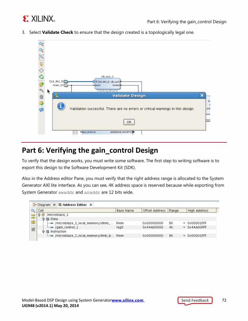
3. Select Validate Check to ensure that the design created is a topologically legal one.
Part 6: Verifying the gain_control Design To verify that the design works, you must write some software. The first step to writing software is to export this design to the Software Development Kit (SDK).
Also in the Address editor Pane, you must verify that the right address range is allocated to the System Generator AXI lite interface. As you can see, 4K address space is reserved because while exporting from System Generator awaddr and araddr are 12 bits wide.
Send Feedback
Part 6: Verifying the gain_control Design
Model-Based DSP Design using System Generatorwww.xilinx.com 73 UG948 (v2014.1) May 20, 2014
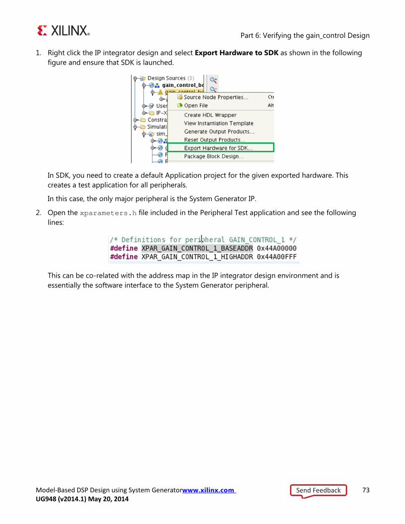
1. Right click the IP integrator design and select Export Hardware to SDK as shown in the following figure and ensure that SDK is launched.
In SDK, you need to create a default Application project for the given exported hardware. This creates a test application for all peripherals.
In this case, the only major peripheral is the System Generator IP.
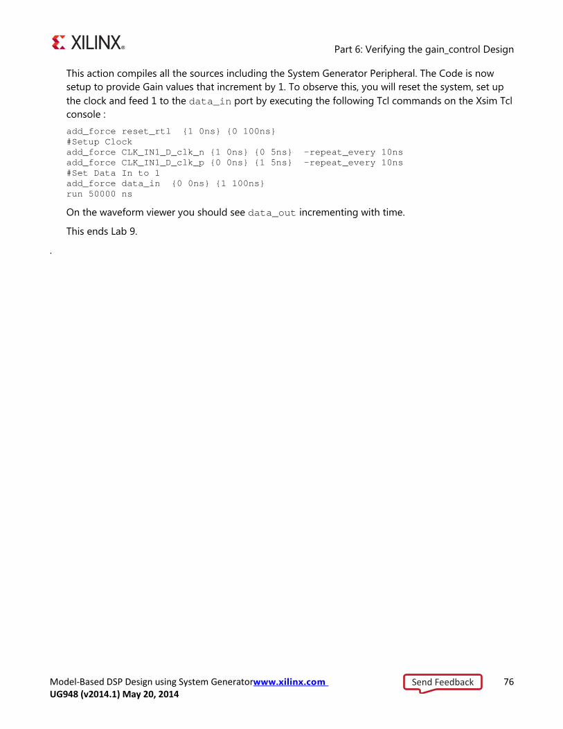
2. Open the xparameters.h file included in the Peripheral Test application and see the following lines:
This can be co-related with the address map in the IP integrator design environment and is essentially the software interface to the System Generator peripheral.
Send Feedback

Part 6: Verifying the gain_control Design
Model-Based DSP Design using System Generatorwww.xilinx.com 74 UG948 (v2014.1) May 20, 2014
3. Modify the Test Peripheral application as shown in the following figure.
4. Save and exit. This creates an ELF file executable.
5. Locate the ELF file and associate as shown in the previous two figures. The ELF file should be located in gain_control.sdk/SDK/SDK_Export/test/Debug/*.elf.
Send Feedback

Part 6: Verifying the gain_control Design
Model-Based DSP Design using System Generatorwww.xilinx.com 75 UG948 (v2014.1) May 20, 2014
6. Launch behavioral simulation.
Send Feedback
Part 6: Verifying the gain_control Design
Model-Based DSP Design using System Generatorwww.xilinx.com 76 UG948 (v2014.1) May 20, 2014
This action compiles all the sources including the System Generator Peripheral. The Code is now setup to provide Gain values that increment by 1. To observe this, you will reset the system, set up the clock and feed 1 to the data_in port by executing the following Tcl commands on the Xsim Tcl console : add_force reset_rtl {1 0ns} {0 100ns} #Setup Clock add_force CLK_IN1_D_clk_n {1 0ns} {0 5ns} -repeat_every 10ns add_force CLK_IN1_D_clk_p {0 0ns} {1 5ns} -repeat_every 10ns #Set Data In to 1 add_force data_in {0 0ns} {1 100ns} run 50000 ns
On the waveform viewer you should see data_out incrementing with time.
This ends Lab 9.
.
Send Feedback
Model-Based DSP Design using System Generatorwww.xilinx.com 77 UG948 (v2014.1) May 20, 2014
Lab 10: Packaging a Synthesized AXI4-Lite Interface
Lab 10 Introduction In this lab, you learn how to package a System Generator design with a synthesized AXI4-Lite interface such that a processor can control the value of registers within the interface ports.
Requirements To complete this lab, you must have the following tools installed:
• Vivado Design Suite System Edition with SDK (v2013.3 or greater)
• MicroZed Hardware Board or any other Xilinx supported Board
Note: You can verify that the SDK tool is installed by navigating to the Xilinx installation directory and observing the SDK folder.
If the SDK folder is not present, download the file named Vivado 2013.3: Standalone SDK Single File Download Image from the www.xilinx.com download area and install the file.
Send Feedback
Procedure
Model-Based DSP Design using System Generatorwww.xilinx.com 78 UG948 (v2014.1) May 20, 2014
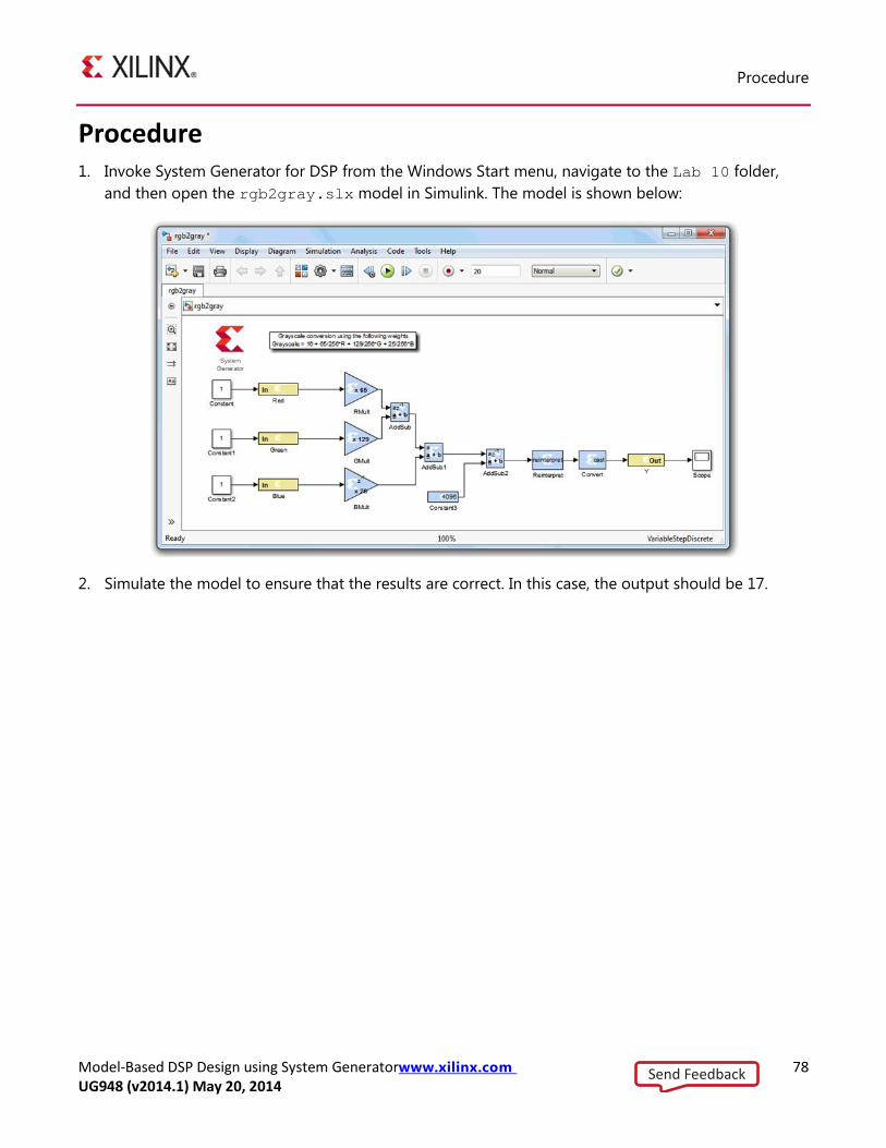
Procedure 1. Invoke System Generator for DSP from the Windows Start menu, navigate to the Lab 10 folder,
and then open the rgb2gray.slx model in Simulink. The model is shown below:
2. Simulate the model to ensure that the results are correct. In this case, the output should be 17.
Send Feedback
Procedure
Model-Based DSP Design using System Generatorwww.xilinx.com 79 UG948 (v2014.1) May 20, 2014
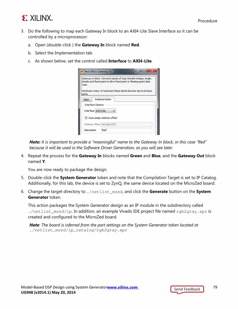
3. Do the following to map each Gateway In block to an AXI4-Lite Slave Interface so it can be controlled by a microprocessor:
a. Open (double-click ) the Gateway In block named Red.
b. Select the Implementation tab.
c. As shown below, set the control called Interface to AXI4-Lite.
Note: It is important to provide a “meaningful” name to the Gateway In block, in this case “Red” because it will be used in the Software Driver Generation, as you will see later.
4. Repeat the process for the Gateway In blocks named Green and Blue, and the Gateway Out block named Y.
You are now ready to package the design.
5. Double-click the System Generator token and note that the Compilation Target is set to IP Catalog. Additionally, for this lab, the device is set to ZynQ, the same device located on the MicroZed board.
6. Change the target directory to ./netlist_mzed, and click the Generate button on the System Generator token.
This action packages the System Generator design as an IP module in the subdirectory called ./netlist_mzed/ip. In addition, an example Vivado IDE project file named rgb2gray.xpr is created and configured to the MicroZed board.
Note: The board is inferred from the part settings on the System Generator token located at ./netlist_mzed/ip_catalog/rgb2gray.xpr
Send Feedback
Procedure
Model-Based DSP Design using System Generatorwww.xilinx.com 80 UG948 (v2014.1) May 20, 2014
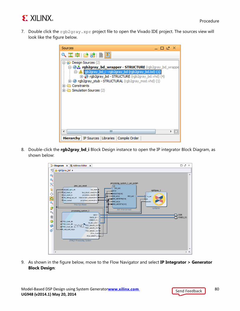
7. Double click the rgb2gray.xpr project file to open the Vivado IDE project. The sources view will look like the figure below.
8. Double-click the rgb2gray_bd_i Block Design instance to open the IP integrator Block Diagram, as shown below:
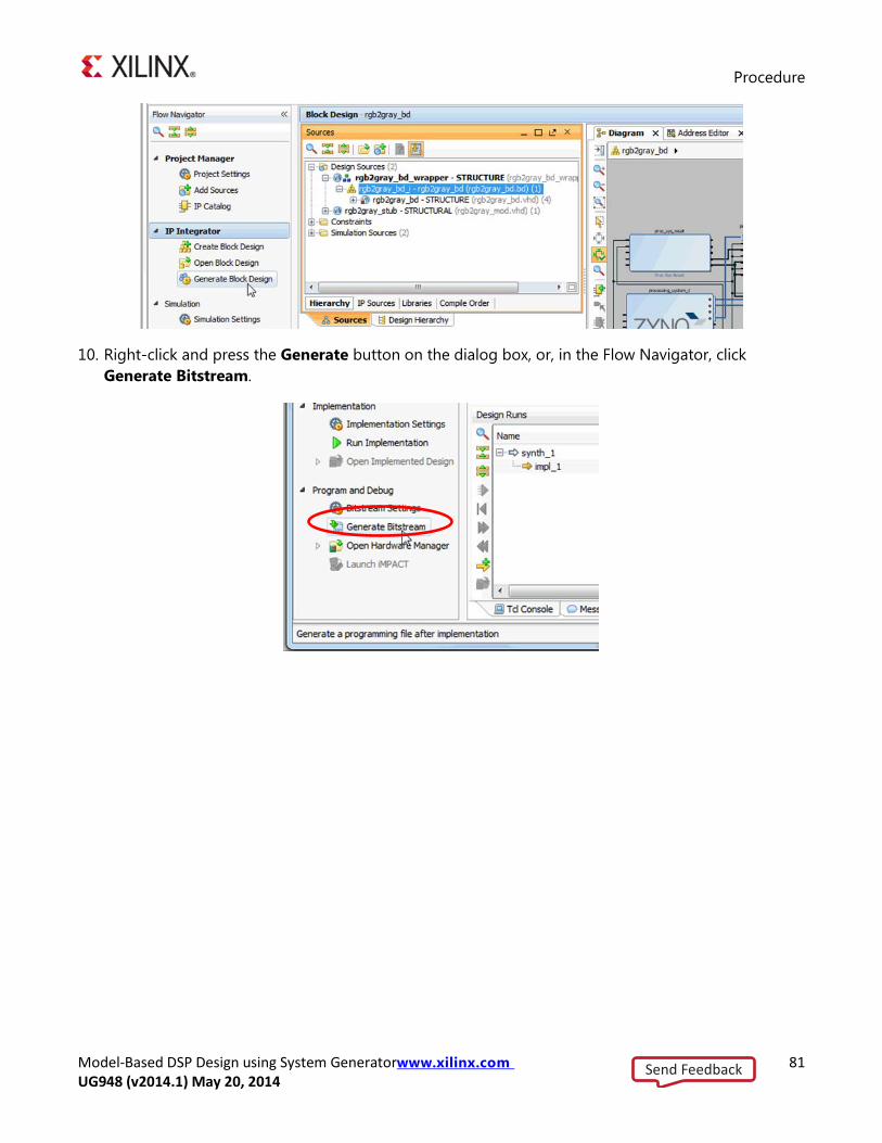
9. As shown in the figure below, move to the Flow Navigator and select IP Integrator > Generator Block Design:
Send Feedback
Procedure
Model-Based DSP Design using System Generatorwww.xilinx.com 81 UG948 (v2014.1) May 20, 2014
10. Right-click and press the Generate button on the dialog box, or, in the Flow Navigator, click Generate Bitstream.
Send Feedback
Procedure
Model-Based DSP Design using System Generatorwww.xilinx.com 82 UG948 (v2014.1) May 20, 2014
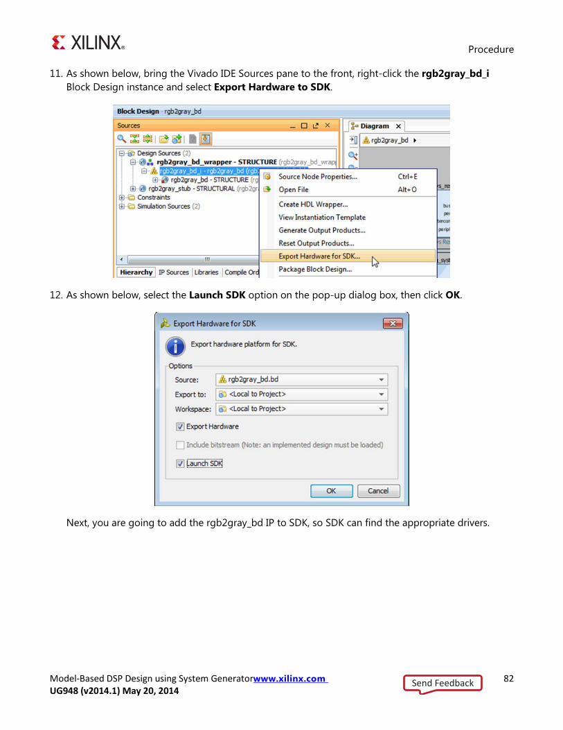
11. As shown below, bring the Vivado IDE Sources pane to the front, right-click the rgb2gray_bd_i Block Design instance and select Export Hardware to SDK.
12. As shown below, select the Launch SDK option on the pop-up dialog box, then click OK.
Next, you are going to add the rgb2gray_bd IP to SDK, so SDK can find the appropriate drivers.
Send Feedback
Procedure
Model-Based DSP Design using System Generatorwww.xilinx.com 83 UG948 (v2014.1) May 20, 2014
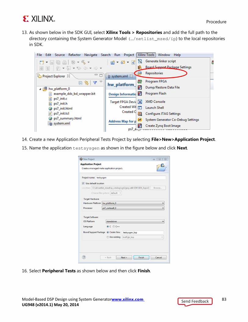
13. As shown below in the SDK GUI, select Xilinx Tools > Repositories and add the full path to the directory containing the System Generator Model (…/netlist_mzed/ip) to the local repositories in SDK.
14. Create a new Application Peripheral Tests Project by selecting File>New>Application Project.
15. Name the application testsysgen as shown in the figure below and click Next.
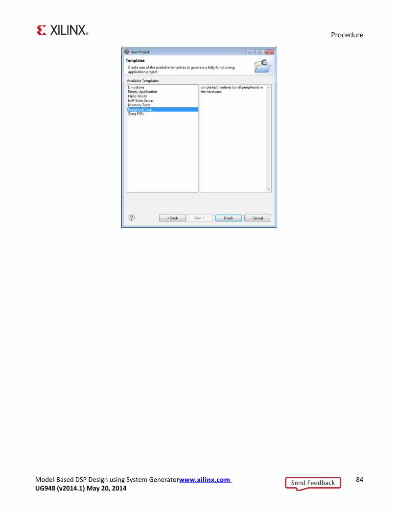
16. Select Peripheral Tests as shown below and then click Finish.
Send Feedback
Procedure
Model-Based DSP Design using System Generatorwww.xilinx.com 84 UG948 (v2014.1) May 20, 2014
Send Feedback
Procedure
Model-Based DSP Design using System Generatorwww.xilinx.com 85 UG948 (v2014.1) May 20, 2014
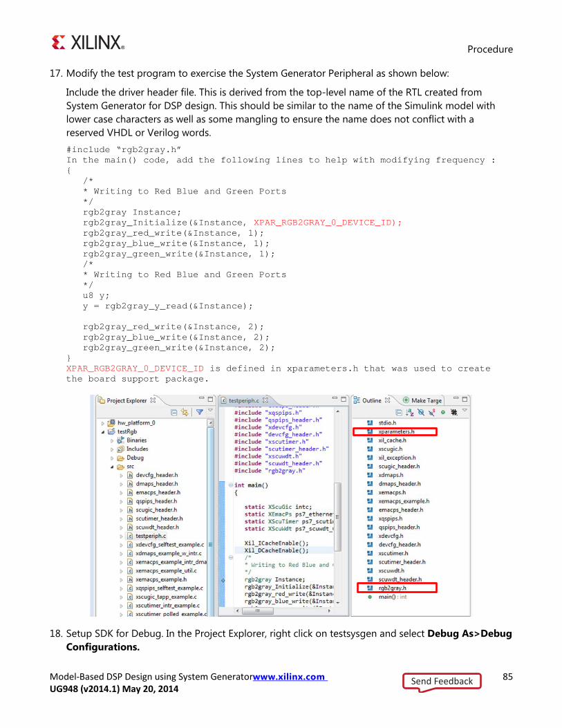
17. Modify the test program to exercise the System Generator Peripheral as shown below:
Include the driver header file. This is derived from the top-level name of the RTL created from System Generator for DSP design. This should be similar to the name of the Simulink model with lower case characters as well as some mangling to ensure the name does not conflict with a reserved VHDL or Verilog words. #include “rgb2gray.h” In the main() code, add the following lines to help with modifying frequency : { /* * Writing to Red Blue and Green Ports */ rgb2gray Instance; rgb2gray_Initialize(&Instance, XPAR_RGB2GRAY_0_DEVICE_ID); rgb2gray_red_write(&Instance, 1); rgb2gray_blue_write(&Instance, 1); rgb2gray_green_write(&Instance, 1); /* * Writing to Red Blue and Green Ports */ u8 y; y = rgb2gray_y_read(&Instance); rgb2gray_red_write(&Instance, 2); rgb2gray_blue_write(&Instance, 2); rgb2gray_green_write(&Instance, 2); } XPAR_RGB2GRAY_0_DEVICE_ID is defined in xparameters.h that was used to create the board support package.
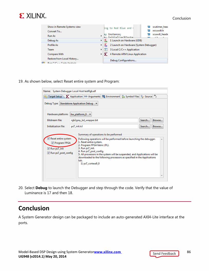
18. Setup SDK for Debug. In the Project Explorer, right click on testsysgen and select Debug As>Debug Configurations.
Send Feedback
Conclusion
Model-Based DSP Design using System Generatorwww.xilinx.com 86 UG948 (v2014.1) May 20, 2014
19. As shown below, select Reset entire system and Program:
20. Select Debug to launch the Debugger and step through the code. Verify that the value of Luminance is 17 and then 18.
Conclusion A System Generator design can be packaged to include an auto-generated AXI4-Lite interface at the ports.
Send Feedback
Example 1 – Importing VHDL into a Black Box
Model-Based DSP Design using System Generatorwww.xilinx.com 87 UG948 (v2014.1) May 20, 2014
Lab 11: Black Box Examples
Example 1 – Importing VHDL into a Black Box
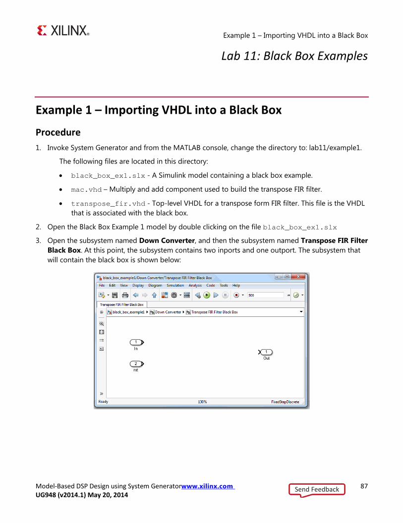
Procedure 1. Invoke System Generator and from the MATLAB console, change the directory to: lab11/example1.
The following files are located in this directory:
• black_box_ex1.slx - A Simulink model containing a black box example.
• mac.vhd – Multiply and add component used to build the transpose FIR filter.
• transpose_fir.vhd - Top-level VHDL for a transpose form FIR filter. This file is the VHDL that is associated with the black box.
2. Open the Black Box Example 1 model by double clicking on the file black_box_ex1.slx
3. Open the subsystem named Down Converter, and then the subsystem named Transpose FIR Filter Black Box. At this point, the subsystem contains two inports and one outport. The subsystem that will contain the black box is shown below:
Send Feedback
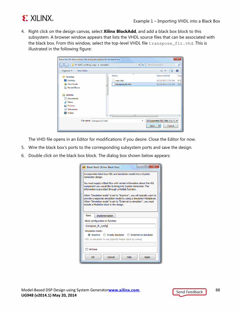
Example 1 – Importing VHDL into a Black Box
Model-Based DSP Design using System Generatorwww.xilinx.com 88 UG948 (v2014.1) May 20, 2014
4. Right click on the design canvas, select Xilinx BlockAdd, and add a black box block to this subsystem. A browser window appears that lists the VHDL source files that can be associated with the black box. From this window, select the top-level VHDL file transpose_fir.vhd. This is illustrated in the following figure:
The VHD file opens in an Editor for modifications if you desire. Close the Editor for now.
5. Wire the black box's ports to the corresponding subsystem ports and save the design.
6. Double click on the black box block. The dialog box shown below appears:
Send Feedback
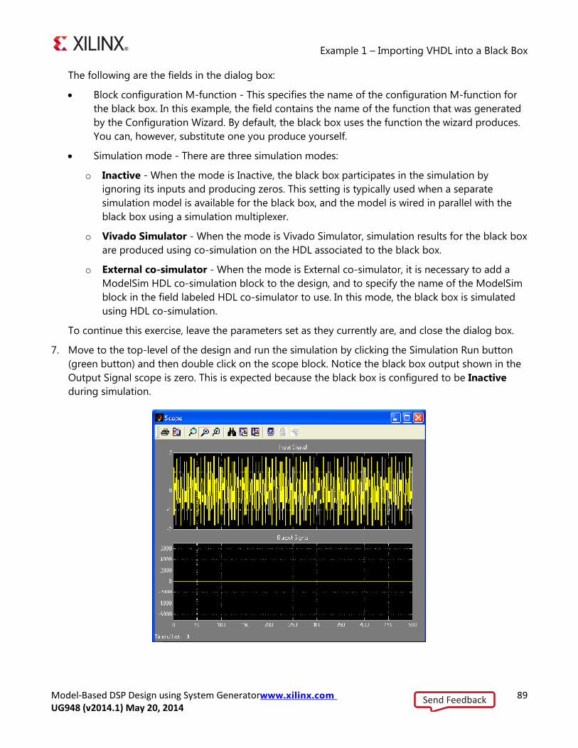
Example 1 – Importing VHDL into a Black Box
Model-Based DSP Design using System Generatorwww.xilinx.com 89 UG948 (v2014.1) May 20, 2014
The following are the fields in the dialog box:
• Block configuration M-function - This specifies the name of the configuration M-function for the black box. In this example, the field contains the name of the function that was generated by the Configuration Wizard. By default, the black box uses the function the wizard produces. You can, however, substitute one you produce yourself.
• Simulation mode - There are three simulation modes:
o Inactive - When the mode is Inactive, the black box participates in the simulation by ignoring its inputs and producing zeros. This setting is typically used when a separate simulation model is available for the black box, and the model is wired in parallel with the black box using a simulation multiplexer.
o Vivado Simulator - When the mode is Vivado Simulator, simulation results for the black box are produced using co-simulation on the HDL associated to the black box.
o External co-simulator - When the mode is External co-simulator, it is necessary to add a ModelSim HDL co-simulation block to the design, and to specify the name of the ModelSim block in the field labeled HDL co-simulator to use. In this mode, the black box is simulated using HDL co-simulation.
To continue this exercise, leave the parameters set as they currently are, and close the dialog box.
7. Move to the top-level of the design and run the simulation by clicking the Simulation Run button (green button) and then double click on the scope block. Notice the black box output shown in the Output Signal scope is zero. This is expected because the black box is configured to be Inactive during simulation.
Send Feedback
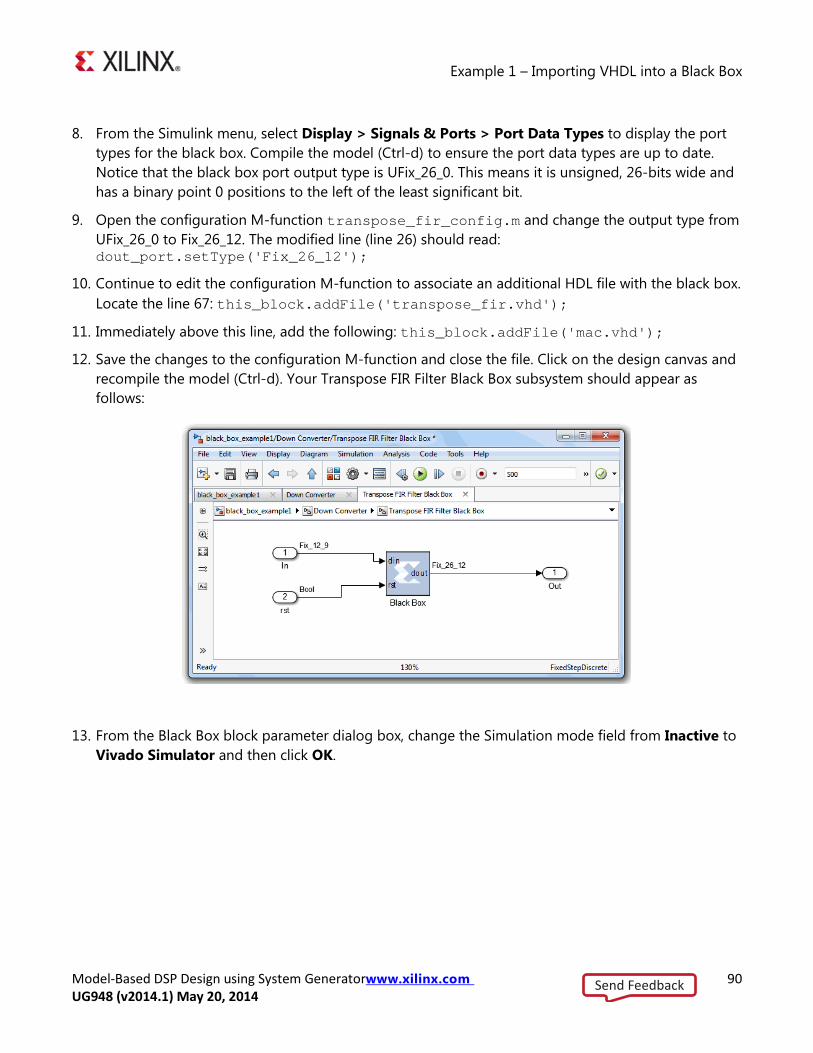
Example 1 – Importing VHDL into a Black Box
Model-Based DSP Design using System Generatorwww.xilinx.com 90 UG948 (v2014.1) May 20, 2014
8. From the Simulink menu, select Display > Signals & Ports > Port Data Types to display the port types for the black box. Compile the model (Ctrl-d) to ensure the port data types are up to date. Notice that the black box port output type is UFix_26_0. This means it is unsigned, 26-bits wide and has a binary point 0 positions to the left of the least significant bit.
9. Open the configuration M-function transpose_fir_config.m and change the output type from UFix_26_0 to Fix_26_12. The modified line (line 26) should read: dout_port.setType('Fix_26_12');
10. Continue to edit the configuration M-function to associate an additional HDL file with the black box. Locate the line 67: this_block.addFile('transpose_fir.vhd');
11. Immediately above this line, add the following: this_block.addFile('mac.vhd');
12. Save the changes to the configuration M-function and close the file. Click on the design canvas and recompile the model (Ctrl-d). Your Transpose FIR Filter Black Box subsystem should appear as follows:
13. From the Black Box block parameter dialog box, change the Simulation mode field from Inactive to Vivado Simulator and then click OK.
Send Feedback

Example 1 – Importing VHDL into a Black Box
Model-Based DSP Design using System Generatorwww.xilinx.com 91 UG948 (v2014.1) May 20, 2014
14. Move to the top-level of the design and run the simulation. Examine the scope output after the simulation has completed. When the Simulation Mode was Inactive, the Output Signal scope displayed constant zero. Notice the waveform is no longer zero. Instead, the Output Signal shows a sine wave as the results from the Vivado Simulation. Right click on the Output Signal canvas and select Autoscale. You should see a display similar to that shown below.
Send Feedback