Embed Size (px)
Citation preview
Sensors and Actuators B, 6 ( 1992) 157- 161 157
Visual images of gas mixtures produced with field-effect structures
F. Winquist, H. Sundgren, E. Hedborg, A. Spetz and I. Lundstriim Laboratory of Applied Physics, Linkliping Institute of Technology, S-581 83 Linkiiping (Sweden)
Abstract
The details of a recently demonstrated possibility of making two-dimensional response maps of a gas mixture are discussed. It is described how maps of work-function changes due to the interaction between molecules like ethanol and ammonia and thin catalytic metal films as gates on field-effect structures can be created with a scanning light-pulse technique. Simple image processing is shown to enhance the differences in the response patterns created by different molecules.
1. Introduction
The use of sensor arrays for odour identifica- tion is now of great interest [l-3]. The odour discrimination is performed through the use of pattern-recognition routines based either on statistical methods or implemented by artificial neural networks to evaluate the data from the sensor array. The arrays tested so far have con- sisted of a limited number of sensors and no sensor tkchnology has yet been developed which enables matrices of similar sizes to be constructed like, for example, charge-coupled devices for optical image formation. One possible shortcut to true ‘olfactory images’ is, however, to use a large continuous sensor surface and a detection principle that allows an imaging of the effects caused by the molecules or ions to be detected on the sensing surface. The sensing surface then needs to have areas of different selectivity and sensitivity to produce an image related to its envi- ronment. In this paper we describe the possibility of using the gas sensitivity of metal-insulator- semiconductor field-effect structures with thin transparent catalytic metal gates [4,5] in combi- nation with a scanning light-pulse technique [6, 71 to monitor the surface potential changes of the semiconductor caused by chemical reactions on the thin metal film. Large area ( ~0.1 - 1 cm*) sensor surfaces with sufficient differences in selec- tivity and sensitivity are easily fabricated using field-effect technology. The scanning light-pulse technique provides a direct imaging of the influ- ence of gas exposure on the electronic properties
09254005/92/$5.00
of the catalytic metal film, which was recently demonstrated [8]. We discuss here the formation of these images in more detail and point out some other possibilities of continuous sensing sur- faces.
2. Scanning light-pulse technique for gas sensing
A pulsed light beam falling through a transpar- ent metal layer on a metal-insulator-semiconduc- tor structure creates a photocapacitive current in the semiconductor, the size of which is determined by the extension of the depletion layer in the semiconductor, as schematically illustrated in Fig. 1. The depletion layer width is determined both by the voltage applied to the metal and the work function of the metal. Furthermore, the current is influenced by (surface) recombination phenomena [6, 71. If the light beam is scanned over the metal surface, in principle an image of the surface poten- tial of the semiconductor can be obtained. The scanned light-pulse technique has been used, for example, to study defects in semiconductor sur- faces [6,7]. In our case we are interested in map- ping the potential changes occurring on the thin metal surface upon gas exposure, as schematically shown in Fig. 2. These potential changes influence the surface potential of the semiconductor and will shift the iph( V) curve along the voltage axis, as illustrated in Fig. l(b). Such an influence is easy to understand. For an ideal metal-insulator-semi- conductor structure the surface potential of the semiconductor is zero when the applied voltage is
@ 1992 - Elsevier Sequoia. All rights reserved

158
XH;O, H,O; 2
AV, v
Ai/ n ;
AV:
Il Light emitting diode
Micro-
element
(4
bh
(b)
Fig. 1. (a) Schematic drawing of the experimental set-up used to
produce two-dimensional response maps to gas mixtures. The drawing
illustrates how a pulsed light beam is used to probe the sensing surface.
The cold end of the sample was x 110 “C and the hot end x 180 “C.
The metals were approximately 6 nm thick and the overlap between
them was 0.5 mm. The total metal area was 4 mm x 6 mm. The dark
line is thick Pd ( x 100 nm) deposited to provide a good electrical
contact. Aluminium was evaporated over the whole backside to
provide a backside constant. (b) Photocapacitive current, iphr as a
function of applied d.c. voltage, V (schematic). The insert illustrates that the photocapacitive current is generated at the semiconductor
surface (in the depletion layer).
equal to the flatband voltage, VFB = (IV, - W,)/q where IV, and IV, are the work functions of the metal and semiconductor, respectively. The surface potential of the semiconductor (or the width of the depletion region and thus also the photocapacitive current) are functions of the difference between the
Insulator (oxide)
Fig. 2. Possible electrical changes of a thin discontinuous metal film due to chemical reactions on the film. AV,, AV, and AV, contribute
to a shift, AV, of the i,,(V) curve along the voltage axis (see Fig. l(b)).
X, Z, Y and A denote (different) chemical species and adsorbates.
applied voltage and the flatband voltage, V - VFB. Exposure to gas changes the ‘effective’ work func- tion of the thin metal film in a rather complicated way, with contributions from A Vi, A I’, and A V, in the general case (A Vi is the shift originating from the metal-insulator interface, AV, is the shift from the metal surface and AV, is the shift originating from the open oxide). We can, however, introduce an equivalent work function change AI+‘, due to these contributions:
AW= -qAV (1)
According to the above discussion, a positive AV therefore leads to a shift of the z&,(V) curve to- wards smaller applied voltages, as illustrated in Fig.
l(b). In our present set-up the light source, an LED
with a lens, was attached to the penholder of an x-y recorder. The xy scan was obtained by apply- ing suitable sawtooth voltages to the x and y inputs respectively. The light output from the LED was modulated at 3 kHz. The diameter of the light spot at the sample was 0.3 mm. The photo- capacitive current from the sample was measured with a lock-in amplifier. The influence of gas expo- sure on the iph( V) curve can be monitored in three ways: by measuring a full iPh( V) curve at each location; measuring iPh at a constant applied voltage; or measuring the voltage necessary to keep a given preset iph. It turns out that the last method, which actually monitors the parallel shift of the iph( V) curve directly, may be preferable, although the measurement of iph is more direct and faster. There are, however, several reasons for the choice of the constant-current mode in general. Figure l(a) showed a schematic of one type of sample used in our investigations. Figure 3 shows
159
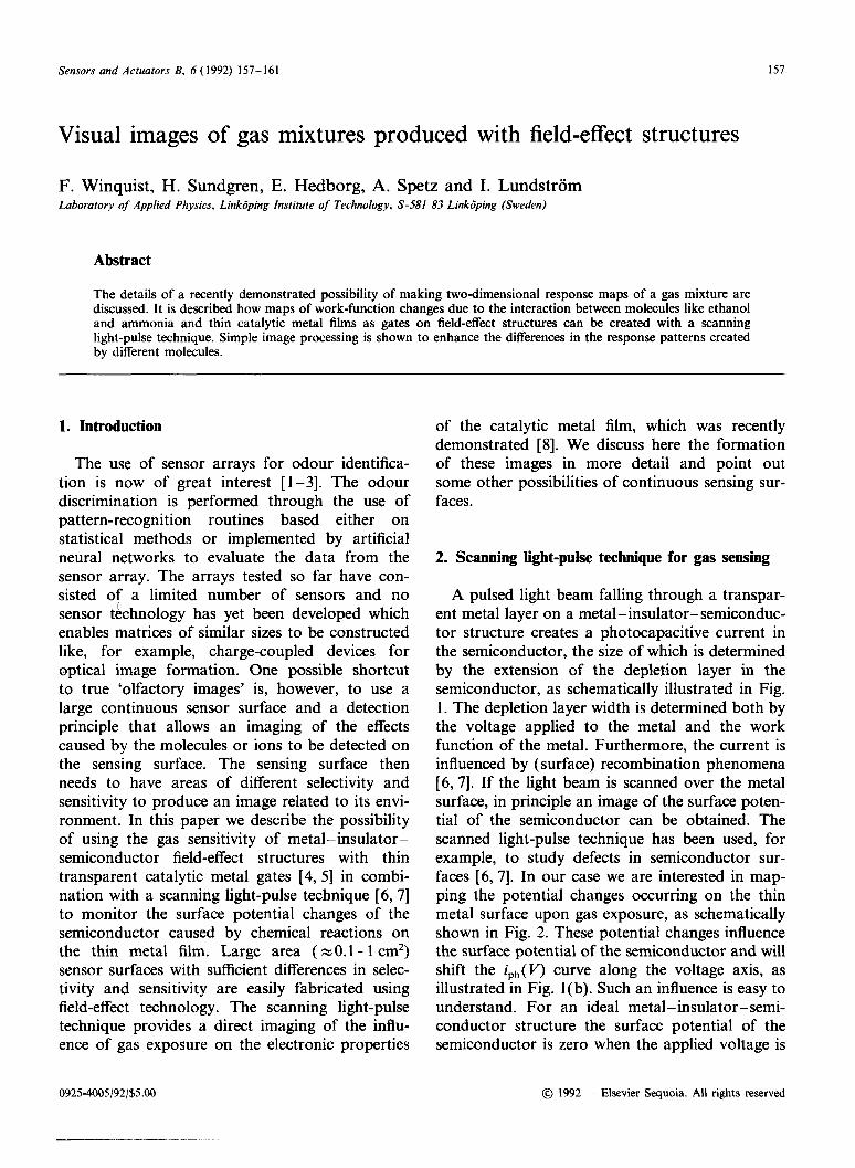
Pd contact
Cold
Fig. 3. Photocurrent at a constant voltage, V, as a function of position for the sample in Fig. I(a) in air. The applied voltage V was chosen to show clearly the different metal areas.
a map of the photocurrent for this structure ex- posed to air only. The different metal areas and their borders are clearly visible. Figure 3 tells us that by choosing a constant applied voltage, the photocurrent will vary along the surface due both to thickness and work function differences along it. The dynamics of the gas detection will therefore depend on where on the iph curve we happen to be at different locations. For a heterogeneous surface it is therefore better to choose a constant current and look for the voltage necessary to keep that current. As long as the gas exposure only induces a parallel shift of the iph( V) curve at a given location, the true shift will be measured regardless of local variations in thickness and initial work function.
mV
1466
1260
1266
(a)
x
1 2 2 4 5 6 mm
Cold and Hot and
3. Experimental details
3.1. Sample structures The test structures consisted of p-type silicon
( 7- 13 Q cm) which was thermally oxidized in dry oxygen at 1200 “C to an oxide thickness of 100 nm. Three different catalytic metals were ther- mally evaporated on top of the oxide through masks to form a pattern as shown schematically in Fig. l(a). The metal layers have to be conducting enough to act as an equipotential surface also at the chopping frequency of the light. Pd, Ir and Pt were chosen as metallizations, since they have proven to be useful as gates on chemical sensors based on field-effect devices [4, 51. Their nominal thicknesses were measured with a quartz-crystal thickness monitor. The test structure was mounted on a kovar plate with a heater at one end (see Fig. l(a)). A temperature gradient was thus created along the metal layers. The temperatures of the cold and hot ends were estimated from the iph( V) characteristics to be about 110 and 180 “C, respec- tively.
3.2. Production of maps of gas-induced voltage shifts
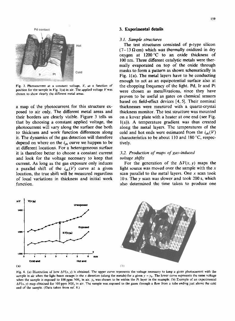
For the generation of the AI+, v) maps the light source was moved over the sample with the x scan parallel to the metal layers. One x scan took 10 s. The y scan was slower and took 200 s, which also determined the time taken to produce one
(b)
Fig. 4. (a) Illustration of how A V(x, y) is obtained. The upper curve represents the voltage necessary to keep a given photocurrent with the sample in air when the light beam sweeps in the x direction (along the metals) for a given y = yO. The lower curve represents the same voltage when the sample is exposed to 100 ppm NH, in air. y0 was chosen to be within the Pt layer in the example. (b) Example of an experimental A V(x, y) map obtained for 100 ppm NH3 in air. The sample was exposed to the gases through a flow from a tube ending just above the cold end of the sample. (Data taken from ref. 8.)
160
Pt Ir Pd Pt Jr Pd Pt k Pd
AMMONIA HYDROGEN ETHANOL
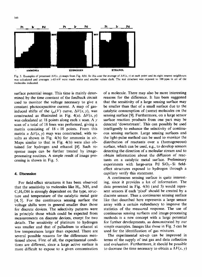
Fig. 5. Examples of processed A Y(x, y) maps from Fig. 4(b). In this case the average of A V(x, y) at each point and its eight nearest neighbours
was calculated and averages >65 mV were made white and smaller values dark. The test structure was exposed to 100 ppm in air of the
molecules indicated.
surface potential image. This time is mainly deter- mined by the time constant of the feedback circuit used to monitor the voltage necessary to give a constant photocapacitive current. A map of gas- induced shifts of the iph( V) curve, AV(x, y), was constructed as illustrated in Fig. 4(a). AV(x, y) was calculated at 18 points along each x scan. A y scan of a total of 18 lines was performed, giving a matrix consisting of 18 x 18 points. From this matrix a AV(x, y) map was constructed, with re- sults as shown in Fig. 4(b) for ammonia in air. Maps similar to that in Fig. 4(b) were also ob- tained for hydrogen and ethanol [8]. Such re- sponse maps can be further treated by image- processing routines. A simple result of image pro- cessing is shown in Fig. 5.
4. Discussion
For field-effect structures it has been observed that the sensitivity to molecules like HZ, NH3 and C2HSOH is strongly dependent on the type, struc- ture and temperature of the catalytic metal gate [4, 51. For the continuous sensing surface the voltage shifts were in general smaller than those for discrete devices. The selectivity patterns were in principle those which could be expected from measurements on discrete devices, except for two details. The sensitivity of platinum to hydrogen was smaller and that of palladium to ethanol at low temperatures larger than expected. There are several possible reasons for the differences men- tioned above. First of all, the experimental condi- tions are different, since a large active surface is more difficult to expose to a given concentration
of a molecule. There may also be more interesting reasons for the difference. It has been suggested that the sensitivity of a large sensing surface may be smaller than that of a small surface due to the catalytic consumption of (some) molecules on the sensing surface [9]. Furthermore, on a large sensor surface reaction products from one part may be detected ‘downstream’. This can possibly be used intelligently to enhance the selectivity of continu- ous sensing surfaces. Large sensing surfaces and the light-pulse method can be used to monitor the distribution of reactants over a (homogeneous) surface, which can be used, e.g., to develop sensors detecting the direction of a moleular stream and to obtain information about the diffusion of reac- tants on a catalytic metal surface. Preliminary experiments with large-area Pd-SiOz-Si field- effect structures exposed to hydrogen through a capillary verify this statement.
A continuous sensing surface is quite interest- ing, since it provides a lot of information. The data presented in Fig. 4(b) (and 5) would repre- sent sensors if each ‘pixel’ should be created by a discrete sensor. Thus a continuous sensing surface like that described here represents a large sensor array with a certain redundancy to improve the statistics of the measured response. The use of continuous sensing surfaces and image-processing methods is a new concept with a large potential for further developments, as demonstrated by our simple examples. Images like those in Fig. 5 can be used for the identification of gas mixtures.
The experimental set-up can be improved in terms of the supply of test gas and data collection and evaluation. Furthermore, it should be possible to decrease the time necessary to obtain a AI/(x, y)
map (200 s). The (scanning) light-pulse technique can be used not only to produce images of gas mixtures but will also be a versatile tool in the testing of new types of chemically sensitive gates on metal-insulator semiconductor structures. Several types of sensing layers can be examined simulta- neously and in the same gas mixture if they are put side by side as in Fig. l(a). Furthermore, a light- pulse technique may be useful for basic studies of (large-area) catalytic metal films. Spatially inhomo- geneous reactions can be mapped, as well as so- called spillover effects on the insulator close to a metal island (or a metal edge).
A continuous sensing surface with two-dimen- sional gradients or changes in selectivity is not limited to thin transparent catalytic metal films. It should be possible, for example, to use conductive polymers or to make gradients in the ion sensitivity of the insulator in a large-area insulator-semicon- ductor structure. The imaging possibilities can also be extended by using other physical methods and sensor structures. Surfaces with gradients in ad- sorption properties, for example, for proteins, can be used together with optical methods, like surface plasmon resonance and ellipsometry, to produce images of molecular interactions on surfaces.
Acknowledgements
Our work on chemical sensors and artificial olfactory images is supported by grants from the
161
Swedish National Board for Industrial and Techni- cal Development, the Swedish Research Council for Engineering Sciences and the Centre for Indus- trial Information Technology, University of Linkoping.
References
H. V. Shurmer, An electronic nose: a sensitive and discriminating
substitute for a mammalian olfactory system, IEE Proc., 137
(1990) G 197-204. T. Nakamoto, K. Fukunishi and T. Monizuma, Identification
capability of odor sensor using quartz-resonator array and neural
network pattern recognition, Sensors and Actuators, El (1990)
431-416.
J. G. Gardner, E. L. Hines and M. Wilkenson, Application of
artificial neural networks to an electronic olfactory system, Meas.
Sci. Technol., I ( 1990) 446-451.
1. Lundstrom, M. Armgarth, A. Spetz and F. Winquist, Gas
sensors based on catalytic-metal-gate field-effect devives, Sensors and Actuators, 10 (1986) 399-421.
1. Lundstrom, A. Spetz, F. Winquist, U. Ackelid and H. Sund-
gren, Catalytic metals and field-effect devices-a useful combina-
tion, Sensors and Actuators, Bl (1990) 15-20. T. H. DiStefano and J. M. Viggiano, Interface imaging by
scanning internal photoemission, IBM J. Res. Deu., 18 (1974)
94-99.
0. Engstrom and A. Carlsson, Scanned light pulse technique for
the investigation of insulator-semiconductor interfaces, J. Appl. Phys., 54 (1983) 5245-5251. I. Lundstrom, R. Erlandsson, U. Frykman, E. Hedborg, A. Spetz,
H. Sundgren, S. Welin and F. Winquist, Artificial ‘olfactory’
images from a chemical sensor using a light pulse technique,
Nature (London), 352 (1991) 47-50.
U. Ackelid and L.-G. Petersson, How a limited mass transfer in
the gas phase may affect the steady-state response of a Pd-
MOS hydrogen sensor, Sensors and Actuators B, 3 (1991) 139- 146.