Embed Size (px)
Citation preview

THS4521 ADS1278 (CH 1)49.9 Ω
1 kΩ 49.9 Ω
VOCM
VIN+
VIN-
5 V
VCOM
1 kΩ
1 kΩ
2.2 nF
AINN1
AINP1
0.1 Fμ0.1 Fμ
x1
1/2OPA2350
1.5 nF
1.5 nF
1 kΩ
0
20
40
60
80
100
120
140
-160
-
-
-
-
-
-
-
Ma
gn
itu
de
(d
BF
S)
0 4 8 12 16 20 24 26
Frequency (kHz)
1-kHz FFT
G = 1R = R = 1 k
C = 1.5 nF
V = 5 V
Load = 2.2 nF
F G
F
S
Ω
Tone
(Hz)
1 k
Signal
(dBFS)
0.50-
SNR (dBc)
109.1
THD (dBc)
107.9-
SINAD
(dBc)
105.5
SFDR
(dBc)
113.7
Product
Folder
Sample &Buy
Technical
Documents
Tools &
Software
Support &Community
THS4521, THS4522, THS4524SBOS458H –DECEMBER 2008–REVISED JUNE 2015
THS452x Very Low Power, Negative Rail Input, Rail-To-Rail Output, Fully DifferentialAmplifier
1 Features 3 DescriptionThe THS4521, THS4522, and THS4524 family of
1• Fully Differential Architecturedevices are very low-power, fully differential• Bandwidth: 145 MHz (AV = 1 V/V) amplifiers with rail-to-rail output and an input
• Slew Rate: 490 V/μs common-mode range that includes the negative rail.These amplifiers are designed for low-power data• HD2: –133 dBc at 10 kHz (1 VRMS, RL = 1 kΩ)acquisition systems and high-density applications• HD3: –141 dBc at 10 kHz (1 VRMS, RL = 1 kΩ) where power dissipation is a critical parameter, and
• Input Voltage Noise: 4.6 nV/√Hz (f = 100 kHz) provide exceptional performance in audioapplications.• THD+N: –112dBc (0.00025%) at 1 kHz (22-kHz
BW, G = 1, 5 VPP) The family includes single FDA (THS4521), dual FDA• Open-Loop Gain: 119 dB (DC) (THS4522), and quad FDA (THS4524) versions.• NRI—Negative Rail Input
Device Information(1)• RRO—Rail-to-Rail Output
PART NUMBER PACKAGE BODY SIZE (NOM)• Output Common-Mode Control (with Low Offset)SOIC (8) 4.90 mm × 3.91 mm
THS4521• Power Supply:VSSOP (8) 3.00 mm × 3.00 mm
– Voltage: +2.5 V (±1.25 V) to +5.5 V (±2.75 V) THS4522 TSSOP (16) 5.00 mm × 4.40 mm– Current: 1.14 mA/ch THS4524 TSSOP (38) 9.70 mm × 4.40 mm
• Power-Down Capability: 20 μA (typical) (1) For all available packages, see the package option addendumat the end of the datasheet.
2 Applications• Low-Power SAR and ΔΣ ADC Drivers• Low-Power Differential Drivers• Low-Power Differential Signal Conditioning• Low-Power, High-Performance Differential Audio
Amplifiers
THS4521 and ADS1278 Combined Performance
For more information on this circuit, view SBAU197.
1
An IMPORTANT NOTICE at the end of this data sheet addresses availability, warranty, changes, use in safety-critical applications,intellectual property matters and other important disclaimers. PRODUCTION DATA.
THS4521, THS4522, THS4524SBOS458H –DECEMBER 2008–REVISED JUNE 2015 www.ti.com
Table of Contents8.3 Feature Description................................................. 251 Features .................................................................. 18.4 Device Functional Modes........................................ 342 Applications ........................................................... 18.5 Programming........................................................... 403 Description ............................................................. 1
9 Application and Implementation ........................ 414 Revision History..................................................... 29.1 Application Information............................................ 415 Device Comparison Table ..................................... 39.2 Typical Applications ............................................... 416 Pin Configuration and Functions ......................... 4
10 Power Supply Recommendations ..................... 517 Specifications......................................................... 711 Layout................................................................... 517.1 Absolute Maximum Ratings ...................................... 7
11.1 Layout Guidelines ................................................. 517.2 ESD Ratings ............................................................ 711.2 Layout Example .................................................... 527.3 Recommended Operating Conditions....................... 7
12 Device and Documentation Support ................. 537.4 Thermal Information .................................................. 712.1 Device Support...................................................... 537.5 Electrical Characteristics: VS+ – VS– = 3.3 V ............ 812.2 Related Links ........................................................ 537.6 Electrical Characteristics: VS+ – VS– = 5 V ............. 1012.3 Community Resources.......................................... 537.7 Typical Characteristics ............................................ 1212.4 Trademarks ........................................................... 537.8 Typical Characteristics: VS+ – VS– = 3.3 V.............. 1412.5 Electrostatic Discharge Caution............................ 537.9 Typical Characteristics: 5 V .................................... 1912.6 Glossary ................................................................ 538 Detailed Description ............................................ 24
13 Mechanical, Packaging, and Orderable8.1 Overview ................................................................. 24Information ........................................................... 538.2 Functional Block Diagram ....................................... 25
4 Revision HistoryNOTE: Page numbers for previous revisions may differ from page numbers in the current version.
Changes from Revision G (December 2014) to Revision H Page
• Changed capacitor units in front page diagram from mF to µF (typo) ................................................................................... 1• Changed RF and RG unit in front page FFT plot from kW to kΩ (typo)................................................................................. 1• Changed Absolute Maximum Ratings minimum storage temperature value from 65 to –65 (typo) ..................................... 7• Added Community Resources section ................................................................................................................................. 53
Changes from Revision F (September 2011) to Revision G Page
• Added Pin Configuration and Functions section, ESD Ratings table, Feature Description section, Device FunctionalModes, Application and Implementation section, Power Supply Recommendations section, Layout section, Deviceand Documentation Support section, and Mechanical, Packaging, and Orderable Information section .............................. 1
Changes from Revision E (December 2010) to Revision F Page
• Changed Input Offset Current values in 3.3 V Electrical Characteristics ............................................................................... 8• Changed Input Offset Current Drift values in 3.3 V Electrical Characteristics ....................................................................... 8• Changed Input Offset Current values in 5 V Electrical Characteristics ................................................................................ 11• Changed Input Offset Current Drift values in 5 V Electrical Characteristics ........................................................................ 11• Changed R41 and R42 in Figure 79..................................................................................................................................... 42
Changes from Revision D (August 2010) to Revision E Page
• Changed test level indication for 5-V input offset voltage drift from B to C.......................................................................... 10
2 Submit Documentation Feedback Copyright © 2008–2015, Texas Instruments Incorporated
Product Folder Links: THS4521 THS4522 THS4524

THS4521, THS4522, THS4524www.ti.com SBOS458H –DECEMBER 2008–REVISED JUNE 2015
5 Device Comparison TableThese fully differential amplifiers feature accurate output common-mode control that allows for dc-coupling whendriving analog-to-digital converters (ADCs). This control, coupled with an input common-mode range below thenegative rail as well as rail-to-rail output, allows for easy interfacing between single-ended, ground-referencedsignal sources. Additionally, these devices are ideally suited for driving both successive-approximation register(SAR) and delta-sigma (ΔΣ) ADCs using only a single +2.5V to +5V and ground power supply.
The THS4521, THS4522, and THS4524 family of fully differential amplifiers is characterized for operation overthe full industrial temperature range from –40°C to +85°C. Table 1 shows a comparison of the THS4521 deviceto similar TI devices.
Table 1. THS4521 Device ComparisonBW IQ THD (dBc) VN DUAL PART
DEVICE (MHz) (mA) AT 100 kHz (nV/√Hz) RAIL-TO-RAIL NUMBERSTHS4531 36 0.25 –104 10.0 Neg In, Out —THS4521 145 0.95 –102 4.6 Neg In, Out THS4522THS4520 620 14.2 –107 2.0 Out —THS4541 850 10.1 –137 2.2 Neg In, Out —
Copyright © 2008–2015, Texas Instruments Incorporated Submit Documentation Feedback 3
Product Folder Links: THS4521 THS4522 THS4524

13
14
15
16
17
18
19
26
25
24
23
22
21
20
VOUT3+
VS3+
VS-
VOUT4-
VOUT4+
VS4+
VIN3+
VIN3-
VOCM3
PD4
VIN4+
VIN4-
VOCM4
9
10
11
12
30
29
28
27
VS2+
VS-
VOUT3-
PD2
PD3
1
2
3
4
5
6
7
8
38
37
36
35
34
33
32
31
VS-
VOUT1-
VOUT1+
VS1+
VS-
VOUT2-
VOUT2+
PD1
VIN1+
VIN1-
VOCM1
VS-
VIN2+
VIN2-
VOCM2
VS-
VS-
VS-
VS-
VS-
1
2
3
4
5
6
7
8
16
15
14
13
12
11
10
9
VS-
VOUT1-
VOUT1+
VS1+
VS-
VOUT2-
VOUT2+
VS2+
PD1
VIN1+
VIN1-
VOCM1
PD2
VIN2+
VIN2-
VOCM2
1
2
3
4
8
7
6
5
VIN+
PD
VS-
VOUT-
VIN-
VOCM
VS+
VOUT+
THS4521, THS4522, THS4524SBOS458H –DECEMBER 2008–REVISED JUNE 2015 www.ti.com
6 Pin Configuration and Functions
THS4521 D and DGK PackageTHS4524 DBT Package8-Pin SOIC and VSSOP
38-Pin TSSOPTop ViewTop View
THS4522 PW Package16-Pin TSSOP
Top View
Pin Functions: THS4521PIN
DESCRIPTIONNAME NO.VIN– 1 Inverting amplifier inputVOCM 2 Common-mode voltage inputVS+ 3 Amplifier positive power-supply inputVOUT+ 4 Noninverting amplifier outputVOUT– 5 Inverting amplifier outputVS– 6 Amplifier negative power-supply input. Note that VS– is tied together on multi-channel devices.PD 7 Power down. PD = logic low puts device into low-power mode. PD = logic high or open for normal operation.VIN+ 8 Noninverting amplifier input
4 Submit Documentation Feedback Copyright © 2008–2015, Texas Instruments Incorporated
Product Folder Links: THS4521 THS4522 THS4524
THS4521, THS4522, THS4524www.ti.com SBOS458H –DECEMBER 2008–REVISED JUNE 2015
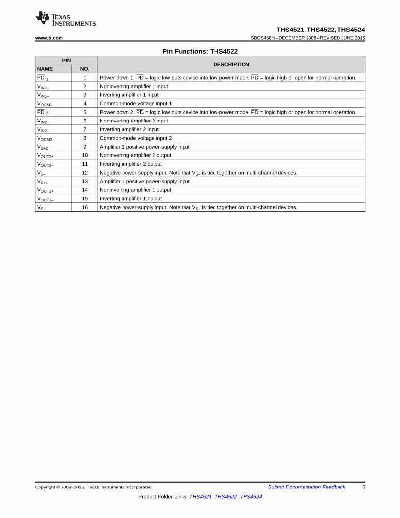
Pin Functions: THS4522PIN
DESCRIPTIONNAME NO.PD 1 1 Power down 1. PD = logic low puts device into low-power mode. PD = logic high or open for normal operation.VIN1+ 2 Noninverting amplifier 1 inputVIN1– 3 Inverting amplifier 1 inputVOCM1 4 Common-mode voltage input 1PD 2 5 Power down 2. PD = logic low puts device into low-power mode. PD = logic high or open for normal operation.VIN2+ 6 Noninverting amplifier 2 inputVIN2– 7 Inverting amplifier 2 inputVOCM2 8 Common-mode voltage input 2VS+2 9 Amplifier 2 positive power-supply inputVOUT2+ 10 Noninverting amplifier 2 outputVOUT2– 11 Inverting amplifier 2 outputVS– 12 Negative power-supply input. Note that VS– is tied together on multi-channel devices.VS+1 13 Amplifier 1 positive power-supply inputVOUT1+ 14 Noninverting amplifier 1 outputVOUT1– 15 Inverting amplifier 1 outputVS– 16 Negative power-supply input. Note that VS– is tied together on multi-channel devices.
Copyright © 2008–2015, Texas Instruments Incorporated Submit Documentation Feedback 5
Product Folder Links: THS4521 THS4522 THS4524

THS4521, THS4522, THS4524SBOS458H –DECEMBER 2008–REVISED JUNE 2015 www.ti.com
Pin Functions: THS4524PIN
DESCRIPTIONNAME NO.PD 1 1 Power down 1. PD = logic low puts channel into low-power mode. PD = logic high or open for normal operation.VIN1+ 2 Noninverting amplifier 1 inputVIN1– 3 Inverting amplifier 1 inputVOCM1 4 Common-mode voltage input 1VS– 5 Negative power-supply input. Note that VS– is tied together on multi-channel devices.PD 2 6 Power down 2. PD = logic low puts channel into low-power mode. PD = logic high or open for normal operation.VIN2+ 7 Noninverting amplifier 2 inputVIN2– 8 Inverting amplifier 2 inputVOCM2 9 Common-mode voltage input 2VS– 10 Negative power-supply input. Note that VS– is tied together on multi-channel devices.PD 3 11 Power down 3. PD = logic low puts channel into low-power mode. PD = logic high or open for normal operation.VIN3+ 12 Noninverting amplifier 3 inputVIN3– 13 Inverting amplifier 3 inputVOCM3 14 Common-mode voltage input 3VS– 15 Negative power-supply input. Note that VS– is tied together on multi-channel devices.PD 4 16 Power down 4. PD = logic low puts channel into low-power mode. PD = logic high or open for normal operation.VIN4+ 17 Noninverting amplifier 4 inputVIN4– 18 Inverting amplifier 4 inputVOCM4 19 Common-mode voltage input 4VS4+ 20 Amplifier 4 positive power-supply inputVOUT4+ 21 Noninverting amplifier 4 outputVOUT4– 22 Inverting amplifier 4 outputVS– 23 Negative power-supply input. Note that VS– is tied together on multi-channel devices.VS– 24 Negative power-supply input. Note that VS– is tied together on multi-channel devices.VS3+ 25 Amplifier 3 positive power-supply inputVOUT3+ 26 Noninverting amplifier3 outputVOUT3– 27 Inverting amplifier3 outputVS– 28 Negative power-supply input. Note that VS– is tied together on multi-channel devices.VS– 29 Negative power-supply input. Note that VS– is tied together on multi-channel devices.VS2+ 30 Amplifier 2 positive power-supply inputVOUT2+ 31 Noninverting amplifier 2 outputVOUT2– 32 Inverting amplifier 2 outputVS– 33 Negative power-supply input. Note that VS– is tied together on multi-channel devices.VS– 34 Negative power-supply input. Note that VS– is tied together on multi-channel devices.VS1+ 35 Amplifier 1 positive power-supply inputVOUT1+ 36 Noninverting amplifier 1 outputVOUT1– 37 Inverting amplifier 1 outputVS– 38 Negative power-supply input. Note that VS– is tied together on multi-channel devices.
6 Submit Documentation Feedback Copyright © 2008–2015, Texas Instruments Incorporated
Product Folder Links: THS4521 THS4522 THS4524

THS4521, THS4522, THS4524www.ti.com SBOS458H –DECEMBER 2008–REVISED JUNE 2015
7 Specifications
7.1 Absolute Maximum RatingsOver operating free-air temperature range (unless otherwise noted). (1)
MIN MAX UNIT
Supply voltage, VS– to VS+ 5.5 V
Input/output voltage, VI (VIN±, VOUT±, VOCM pins) (VS–) – 0.7 (VS+) + 0.7 V
Differential input voltage, VID 1 V
Output current, IO 100 mA
Input current, II (VIN±, VOCM pins) 10 mA
Continuous power dissipation See Thermal Information table
Maximum junction temperature, TJ 150 °C
Maximum junction temperature, TJ (continuous operation, long-term reliability) 125 °C
Operating free-air temperature, TA –40 85 °C
Storage temperature, Tstg –65 150 °C
(1) Stresses beyond those listed under Absolute Maximum Ratings may cause permanent damage to the device. These are stress ratingsonly, which do not imply functional operation of the device at these or any other conditions beyond those indicated under RecommendedOperating Conditions. Exposure to absolute-maximum-rated conditions for extended periods may affect device reliability.
7.2 ESD RatingsVALUE UNIT
Human body model (HBM), per ANSI/ESDA/JEDEC JS-001, all pins (1) ±1300ElectrostaticV(ESD) Charged device model (CDM), per JEDEC specification JESD22-C101, all pins (2) ±1000 Vdischarge
Machine model (MM) ±50
(1) JEDEC document JEP155 states that 500-V HBM allows safe manufacturing with a standard ESD control process.(2) JEDEC document JEP157 states that 250-V CDM allows safe manufacturing with a standard ESD control process.
7.3 Recommended Operating Conditionsover operating free-air temperature range (unless otherwise noted)
MIN NOM MAX UNITVS+ single-supply voltage 2.7 5.0 5.4 VTA Ambient temperature –40 25 85 °C
7.4 Thermal InformationTHS4521 THS4522 THS4524
THERMAL METRIC (1) D DGK PW DBT UNIT8 PINS 8 PINS 16 PINS 38 PINS
RθJA Junction-to-ambient thermal resistance 127.8 193.8 124.2 106.2RθJC(top) Junction-to-case (top) thermal resistance 81.8 84.1 62.8 60.9RθJB Junction-to-board thermal resistance 68.3 115.3 68.5 65.5
°C/WψJT Junction-to-top characterization parameter 32.2 17.9 15.8 18.5ψJB Junction-to-board characterization parameter 67.8 113.6 68 65.1RθJC(bot) Junction-to-case (bottom) thermal resistance N/A N/A N/A N/A
(1) For more information about traditional and new thermal metrics, see the IC Package Thermal Metrics application report, SPRA953.
Copyright © 2008–2015, Texas Instruments Incorporated Submit Documentation Feedback 7
Product Folder Links: THS4521 THS4522 THS4524

THS4521, THS4522, THS4524SBOS458H –DECEMBER 2008–REVISED JUNE 2015 www.ti.com
7.5 Electrical Characteristics: VS+ – VS– = 3.3 VAt VS+ = 3.3 V, VS– = 0 V, VOCM = open, VOUT = 2 VPP (differential), RL = 1 kΩ differential, G = 1 V/V, single-ended input,differential output, and input and output referenced to midsupply, unless otherwise noted.
TESTPARAMETER TEST CONDITIONS LEVEL (1) MIN TYP MAX UNIT
AC PERFORMANCE
VOUT = 100 mVPP, G = 1 C 135 MHz
VOUT = 100 mVPP, G = 2 C 49 MHzSmall-signal bandwidth
VOUT = 100 mVPP, G = 5 C 18.6 MHz
VOUT = 100 mVPP, G = 10 C 9.3 MHz
Gain bandwidth product VOUT = 100 mVPP, G = 10 C 93 MHz
Large-signal bandwidth VOUT = 2 VPP, G = 1 C 95 MHz
Bandwidth for 0.1-dB flatness VOUT = 2 VPP, G = 1 C 20 MHz
Rising slew rate (differential) VOUT = 2-V Step, G = 1, RL = 200 Ω C 420 V/μs
Falling slew rate (differential) VOUT = 2-V Step, G = 1, RL = 200 Ω C 460 V/μs
Overshoot VOUT = 2-V Step, G = 1, RL = 200 Ω C 1.2%
Undershoot VOUT = 2-V Step, G = 1, RL = 200 Ω C 2.1%
Rise time VOUT = 2-V Step, G = 1, RL = 200 Ω C 4 ns
Fall time VOUT = 2-V Step, G = 1, RL = 200 Ω C 3.5 ns
Settling time to 1% VOUT = 2-V Step, G = 1, RL = 200 Ω C 13 ns
HARMONIC DISTORTION
f = 1 MHz, VOUT = 2 VPP, G = 1 C –85 dBc2nd harmonic f = 1 kHz, VOUT = 1 VRMS, G = 1 (2), C –133 dBcdifferential input
f = 1 MHz, VOUT = 2 VPP, G = 1 C –90 dBc3rd harmonic f = 1 kHz, VOUT = 1 VRMS, G = 1 (2), C –141 dBcdifferential input
Two-tone, f1 = 2 MHz, f2 = 2.2 MHz,Second-order intermodulation distortion C –83 dBcVOUT = 2-VPP envelope
Two-tone, f1 = 2 MHz, f2 = 2.2 MHz,Third-order intermodulation distortion C –90 dBcVOUT = 2-VPP envelope
Input voltage noise f > 10 kHz C 4.6 nV/√Hz
Input current noise f > 100 kHz C 0.6 pA/√Hz
Overdrive recovery time Overdrive = ±0.5 V C 80 ns
Output balance error VOUT = 100 mV, f ≤ 2 MHz (differential input) C –57 dB
Closed-loop output impedance f = 1 MHz (differential) C 0.3 Ω
Channel-to-channel crosstalk (THS4522, f = 10 kHz, measured differentially C –125 dBTHS4524)
DC PERFORMANCE
Open-loop voltage gain (AOL) A 100 116 dB
TA = +25°C A ±0.2 ±2 mVInput-referred offset voltage
TA = –40°C to +85°C B ±0.5 ±3.5 mV
Input offset voltage drift (3) TA = –40°C to +85°C C ±2 μV/°C
TA = +25°C B 0.65 0.85 μAInput bias current (4)
TA = –40°C to +85°C B 0.75 0.95 μA
Input bias current drift (3) TA = –40°C to +85°C B ±1.75 ±2 nA/°C
TA = +25°C B ±30 ±180 nAInput offset current
TA = –40°C to +85°C B ±30 ±215 nA
Input offset current drift (3) TA = –40°C to +85°C B ±100 ±600 pA/°C
(1) Test levels: (A) 100% tested at 25°C. Over temperature limits set by characterization and simulation. (B) Limits set by characterizationand simulation. (C) Typical value only for information.
(2) Not directly measurable; calculated using noise gain of 101 as described in the Applications section, Audio Performance.(3) Input offset voltage drift, input bias current drift, input offset current drift, and VOCM drift are average values calculated by taking data at
the maximum-range ambient-temperature end points, computing the difference, and dividing by the temperature range. Maximum drift isset by the distribution of a large sampling of devices. Drift is not specified by a test or a quality assurance (QA) sample test.
(4) Input bias current is positive out of the device.
8 Submit Documentation Feedback Copyright © 2008–2015, Texas Instruments Incorporated
Product Folder Links: THS4521 THS4522 THS4524
THS4521, THS4522, THS4524www.ti.com SBOS458H –DECEMBER 2008–REVISED JUNE 2015
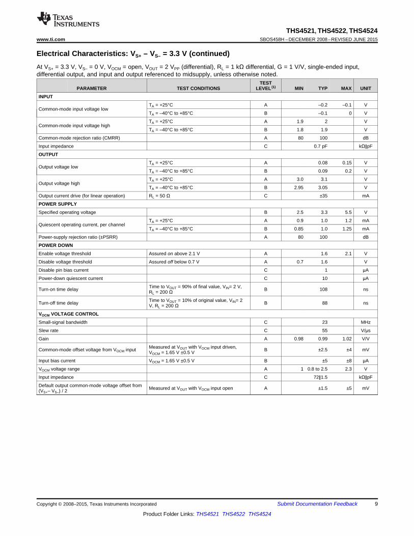
Electrical Characteristics: VS+ – VS– = 3.3 V (continued)At VS+ = 3.3 V, VS– = 0 V, VOCM = open, VOUT = 2 VPP (differential), RL = 1 kΩ differential, G = 1 V/V, single-ended input,differential output, and input and output referenced to midsupply, unless otherwise noted.
TESTPARAMETER TEST CONDITIONS LEVEL (1) MIN TYP MAX UNIT
INPUT
TA = +25°C A –0.2 –0.1 VCommon-mode input voltage low
TA = –40°C to +85°C B –0.1 0 V
TA = +25°C A 1.9 2 VCommon-mode input voltage high
TA = –40°C to +85°C B 1.8 1.9 V
Common-mode rejection ratio (CMRR) A 80 100 dB
Input impedance C 0.7 pF kΩ∥pF
OUTPUT
TA = +25°C A 0.08 0.15 VOutput voltage low
TA = –40°C to +85°C B 0.09 0.2 V
TA = +25°C A 3.0 3.1 VOutput voltage high
TA = –40°C to +85°C B 2.95 3.05 V
Output current drive (for linear operation) RL = 50 Ω C ±35 mA
POWER SUPPLY
Specified operating voltage B 2.5 3.3 5.5 V
TA = +25°C A 0.9 1.0 1.2 mAQuiescent operating current, per channel
TA = –40°C to +85°C B 0.85 1.0 1.25 mA
Power-supply rejection ratio (±PSRR) A 80 100 dB
POWER DOWN
Enable voltage threshold Assured on above 2.1 V A 1.6 2.1 V
Disable voltage threshold Assured off below 0.7 V A 0.7 1.6 V
Disable pin bias current C 1 μA
Power-down quiescent current C 10 μA
Time to VOUT = 90% of final value, VIN= 2 V,Turn-on time delay B 108 nsRL = 200 Ω
Time to VOUT = 10% of original value, VIN= 2Turn-off time delay B 88 nsV, RL = 200 Ω
VOCM VOLTAGE CONTROL
Small-signal bandwidth C 23 MHz
Slew rate C 55 V/μs
Gain A 0.98 0.99 1.02 V/V
Measured at VOUT with VOCM input driven,Common-mode offset voltage from VOCM input B ±2.5 ±4 mVVOCM = 1.65 V ±0.5 V
Input bias current VOCM = 1.65 V ±0.5 V B ±5 ±8 μA
VOCM voltage range A 1 0.8 to 2.5 2.3 V
Input impedance C 72∥1.5 kΩ∥pF
Default output common-mode voltage offset from Measured at VOUT with VOCM input open A ±1.5 ±5 mV(VS+– VS–) / 2
Copyright © 2008–2015, Texas Instruments Incorporated Submit Documentation Feedback 9
Product Folder Links: THS4521 THS4522 THS4524

THS4521, THS4522, THS4524SBOS458H –DECEMBER 2008–REVISED JUNE 2015 www.ti.com
7.6 Electrical Characteristics: VS+ – VS– = 5 VAt VS+ = 5 V, VS– = 0 V, VOCM = open, VOUT = 2 VPP (differential), RF = 1 kΩ, RL = 1 kΩ differential, G = 1 V/V, single-endedinput, differential output, input and output referenced to midsupply, unless otherwise noted.
TESTPARAMETER TEST CONDITIONS LEVEL (1) MIN TYP MAX UNIT
AC PERFORMANCE
VOUT = 100 mVPP, G = 1 C 145 MHz
VOUT = 100 mVPP, G = 2 C 50 MHzSmall-signal bandwidth
VOUT = 100 mVPP, G = 5 C 20 MHz
VOUT = 100 mVPP, G = 10 C 9.5 MHz
Gain bandwidth product VOUT = 100 mVPP, G = 10 C 95 MHz
Large-signal bandwidth VOUT = 2 VPP, G = 1 C 145 MHz
Bandwidth for 0.1-dB flatness VOUT = 2 VPP, G = 1 C 30 MHz
Rising slew rate (differential) VOUT = 2-V Step, G = 1, RL = 200 Ω C 490 V/μs
Falling slew rate (differential) VOUT = 2-V Step, G = 1, RL = 200 Ω C 600 V/μs
Overshoot VOUT = 2-V Step, G = 1, RL = 200 Ω C 1%
Undershoot VOUT = 2-V Step, G = 1, RL = 200 Ω C 2.6%
Rise time VOUT = 2-V Step, G = 1, RL = 200 Ω C 3.4 ns
Fall time VOUT = 2-V Step, G = 1, RL = 200 Ω C 3 ns
Settling time to 1% VOUT = 2-V Step, G = 1, RL = 200 Ω C 10 ns
HARMONIC DISTORTION
f = 1 MHz, VOUT = 2 VPP, G = 1 C –85 dBc2nd harmonic f = 1 kHz, VOUT = 1 VRMS, G = 1 (2), C –133 dBcdifferential input
f = 1 MHz, VOUT = 2 VPP, G = 1 C –91 dBc3rd harmonic f = 1 kHz, VOUT = 1 VRMS, G = 1 (2), C –141 dBcdifferential input
Two-tone, f1 = 2 MHz, f2 = 2.2 MHz,Second-order intermodulation distortion C –86 dBcVOUT = 2-VPP envelope
Two-tone, f1 = 2 MHz, f2 = 2.2 MHz,Third-order intermodulation distortion C –93 dBcVOUT = 2-VPP envelope
Input voltage noise f > 10 kHz C 4.6 nV/√Hz
Input current noise f > 100 kHz C 0.6 pA/√Hz
VOUT = 5 VPP, 20 Hz to 22 kHz BW,SNR C 123 dBcdifferential input
f = 1 kHz , VOUT = 5 VPP, 20 Hz to 22 kHzTHD+N C 112 dBcBW, differential input
Overdrive recovery time Overdrive = ±0.5 V C 75 ns
Output balance error VOUT = 100 mV, f < 2 MHz, VIN differential C –57 dB
Closed-loop output impedance f = 1 MHz (differential) C 0.3 Ω
Channel-to-channel crosstalk (THS4522. THS4524) f = 10 kHz, measured differentially C –125 dB
DC PERFORMANCE
Open-loop voltage gain (AOL) A 100 119 dB
TA = +25°C A ±0.24 ±2 mVInput-referred offset voltage
TA = –40°C to +85°C B ±0.5 ±3.5 mV
Input offset voltage drift (3) TA = –40°C to +85°C C ±2 μV/°C
TA = +25°C B 0.7 0.9 μAInput bias current (4)
TA = –40°C to +85°C B 0.9 1.1 μA
Input bias current drift (3) TA = –40°C to +85°C B ±1.8 ±2.2 nA/°C
(1) Test levels: (A) 100% tested at 25°C. Over temperature limits set by characterization and simulation. (B) Limits set by characterizationand simulation. (C) Typical value only for information.
(2) Not directly measurable; calculated using noise gain of 101 as described in the Applications section, Audio Performance.(3) Input offset voltage drift, input bias current drift, input offset current drift, and VOCM drift are average values calculated by taking data at
the maximum-range ambient-temperature end points, computing the difference, and dividing by the temperature range. Maximum drift isset by the distribution of a large sampling of devices. Drift is not specified by a test or a quality assurance (QA) sample test.
(4) Input bias current is positive out of the device.
10 Submit Documentation Feedback Copyright © 2008–2015, Texas Instruments Incorporated
Product Folder Links: THS4521 THS4522 THS4524

THS4521, THS4522, THS4524www.ti.com SBOS458H –DECEMBER 2008–REVISED JUNE 2015
Electrical Characteristics: VS+ – VS– = 5 V (continued)At VS+ = 5 V, VS– = 0 V, VOCM = open, VOUT = 2 VPP (differential), RF = 1 kΩ, RL = 1 kΩ differential, G = 1 V/V, single-endedinput, differential output, input and output referenced to midsupply, unless otherwise noted.
TESTPARAMETER TEST CONDITIONS LEVEL (1) MIN TYP MAX UNIT
TA = +25°C B ±30 ±180 nAInput offset current
TA = –40°C to +85°C B ±30 ±215 nA
Input offset current drift (3) TA = –40°C to +85°C B ±100 ±600 pA/°C
INPUT
TA = +25°C A –0.2 –0.1 VCommon-mode input voltage low
TA = –40°C to +85°C B –0.1 0 V
TA = +25°C A 3.6 3.7 VCommon-mode input voltage high
TA = –40°C to +85°C B 3.5 3.6 V
Common-mode rejection ratio (CMRR) A 80 102 dB
Input impedance C 100∥0.7 kΩ∥pF
OUTPUT
TA = +25°C A 0.10 0.15 VOutput voltage low
TA = –40°C to +85°C B 0.115 0.2 V
TA = +25°C A 4.7 4.75 VOutput voltage high
TA = –40°C to +85°C B 4.65 4.7 V
Output current drive (for linear operation) RL = 50 Ω C ±55 mA
POWER SUPPLY
Specified operating voltage B 2.5 5.0 5.5 V
TA = +25°C A 0.95 1.14 1.25 mAQuiescent operating current, per channel
TA = –40°C to +85°C B 0.9 1.15 1.3 mA
Power-supply rejection ratio (±PSRR) A 80 100 dB
POWER DOWN
Enable voltage threshold Ensured on above 2.1 V A 1.6 2.1 V
Disable voltage threshold Ensured off below 0.7 V A 0.7 1.6 V
Disable pin bias current C 1 μA
Power-down quiescent current C 20 μA
Time to VOUT = 90% of final value,Turn-on time delay B 70 nsVIN= 2 V, RL = 200 Ω
Time to VOUT = 10% of original value,Turn-off time delay B 60 nsVIN= 2 V, RL = 200 Ω
VOCM VOLTAGE CONTROL
Small-signal bandwidth C 23 MHz
Slew rate C 55 V/μs
Gain A 0.98 0.99 1.02 V/V
Measured at VOUT with VOCM input driven,Common-mode offset voltage from VOCM input B ±5 ±9 mVVOCM = 2.5 V ±1 V
Input bias current VOCM = 2.5V ±1 V B ±20 ±25 μA
VOCM voltage range A 1 0.8 to 4.2 4 V
Input impedance C 46∥1.5 kΩ∥pF
Default output common-mode voltage offset from Measured at VOUT with VOCM input open A ±1 ±5 mV(VS+– VS–) / 2
Copyright © 2008–2015, Texas Instruments Incorporated Submit Documentation Feedback 11
Product Folder Links: THS4521 THS4522 THS4524

THS4521, THS4522, THS4524SBOS458H –DECEMBER 2008–REVISED JUNE 2015 www.ti.com
7.7 Typical Characteristics
Table 2. Table of Graphs: VS+ – VS– = 3.3 VFIGURE
Small-Signal Frequency Response Figure 1Large-Signal Frequency Response Figure 2Large- and Small-Signal Pulse Response Figure 3Slew Rate vs VOUT Step Figure 4Overdrive Recovery Figure 510-kHz Output Spectrum on AP Analyzer Figure 6Harmonic Distortion vs Frequency Figure 7Harmonic Distortion vs Output Voltage at 1 MHz Figure 8Harmonic Distortion vs Gain at 1 MHz Figure 9Harmonic Distortion vs Load at 1 MHz Figure 10Harmonic Distortion vs VOCM at 1 MHz Figure 11Two-Tone, Second- and Third-Order Intermodulation Distortion vs Frequency Figure 12Single-Ended Output Voltage Swing vs Load Resistance Figure 13Main Amplifier Differential Output Impedance vs Frequency Figure 14Frequency Response vs CLOAD (RLOAD = 1 kΩ) Figure 15RO vs CLOAD (RLOAD = 1 kΩ) Figure 16Rejection Ratio vs Frequency Figure 17THS4522, THS4524 Crosstalk (Measured Differentially) Figure 18Turn-on Time Figure 19Turn-off Time Figure 20Input-Referred Voltage Noise and Current Noise Spectral Density Figure 21Main Amplifier Differential Open-Loop Gain and Phase Figure 22Output Balance Error vs Frequency Figure 23VOCM Small-Signal Frequency Response Figure 24VOCM Large-Signal Frequency Response Figure 25VOCM Input Impedance vs Frequency Figure 26
12 Submit Documentation Feedback Copyright © 2008–2015, Texas Instruments Incorporated
Product Folder Links: THS4521 THS4522 THS4524

THS4521, THS4522, THS4524www.ti.com SBOS458H –DECEMBER 2008–REVISED JUNE 2015
Table 3. Table of Graphs: VS+ – VS– = 5 VFIGURE
Small-Signal Frequency Response Figure 27Large-Signal Frequency Response Figure 28Large- and Small-Signal Pulse Response Figure 29Slew Rate vs VOUT Step Figure 30Overdrive Recovery Figure 3110-kHz Output Spectrum on AP Analyzer Figure 33Harmonic Distortion vs Frequency Figure 34Harmonic Distortion vs Output Voltage at 1 MHz Figure 35Harmonic Distortion vs Gain at 1 MHz Figure 36Harmonic Distortion vs Load at 1 MHz Figure 37Harmonic Distortion vs VOCM at 1 MHz Figure 38Two-Tone, Second- and Third-Order Intermodulation Distortion vs Frequency Figure 39Single-Ended Output Voltage Swing vs Load Resistance Figure 40Main Amplifier Differential Output Impedance vs Frequency Figure 41Frequency Response vs CLOAD (RLOAD = 1 kΩ) Figure 42RO vs CLOAD (RLOAD = 1 kΩ) Figure 43Rejection Ratio vs Frequency Figure 44THS4522, THS4524 Crosstalk (Measured Differentially) Figure 45Turn-on Time Figure 46Turn-off Time Figure 47Input-Referred Voltage Noise and Current Noise Spectral Density Figure 48Main Amplifier Differential Open-Loop Gain and Phase Figure 49Output Balance Error vs Frequency Figure 50VOCM Small-Signal Frequency Response Figure 51VOCM Large-Signal Frequency Response Figure 52VOCM Input Impedance vs Frequency Figure 53
Copyright © 2008–2015, Texas Instruments Incorporated Submit Documentation Feedback 13
Product Folder Links: THS4521 THS4522 THS4524

4
3
2
1
0
1
2
3
4
-
-
-
-
2.0
1.5
1.0
0.5
0
0.5
1.0
1.5
2.0
-
-
-
-
Diffe
rential V
(V)
OU
T
Input V
olta
ge (V
)
0 100 200 300 400 500 600 800 900 1 k
Time (ns)
V = 3.3 V
G = 2 V/V
R = 1 k
S+
F W
R = 200L W
V Diff
InputOUT
10
0
-10
20
30
40
50
60
70
80
90
100
110
120
130
140
-
-
-
-
-
-
-
-
-
-
-
-
-
Ma
gn
itu
de
(d
Bv)
0 5 k 10 k 15 k 20 k 25 k 30 k 35 k
Frequency (Hz)
THS4521V = 3.3 V
G = 1 V/VR = 1 kW
V = 5 V
S+
F
OUT PP
1.5
1.0
0.5
0
0.5
1.0
1.5
-
-
-
Diffe
ren
tia
l V
(V)
OU
T
0 20 40 60 80 100
Time (ns)
2-V Step
0.5-V Step
V = 3.3 V
G = 1 V/V
R = 1 k
R = 200
S+
F
L
W
W
600
500
400
300
200
100
0
0 1 2 3 4 5
Differential V (V)OUT
Sle
w R
ate
(V
/s)
m
V = 3.3 V
G = 1 V/V
R = 1 k
S+
F W
R = 200L W
Rising
Falling
6
3
0
3
6
9
12
15
18
21
24
-
-
-
-
-
-
-
-
100 k 1 M 10 M 100 M 1 G
Frequency (Hz)
No
rma
lize
d G
ain
(d
B)
G = 1 V/V
G = 2 V/V
G = 5 V/V
G = 10 V/V
V = 3.3 V
R = 1 k
V = 100 mV
S+
L
O PP
W
6
3
0
3
6
9
12
15
18
21
24
-
-
-
-
-
-
-
-
No
rma
lize
d G
ain
(d
B)
100 k 1 M 10 M 100 M 1 G
Frequency (Hz)
V = 3.3 V
R = 1 k
V = 2.0 V
S+
L
O PP
W
G = 1 V/V
G = 2 V/V
G = 5 V/V
G = 10 V/V
THS4521, THS4522, THS4524SBOS458H –DECEMBER 2008–REVISED JUNE 2015 www.ti.com
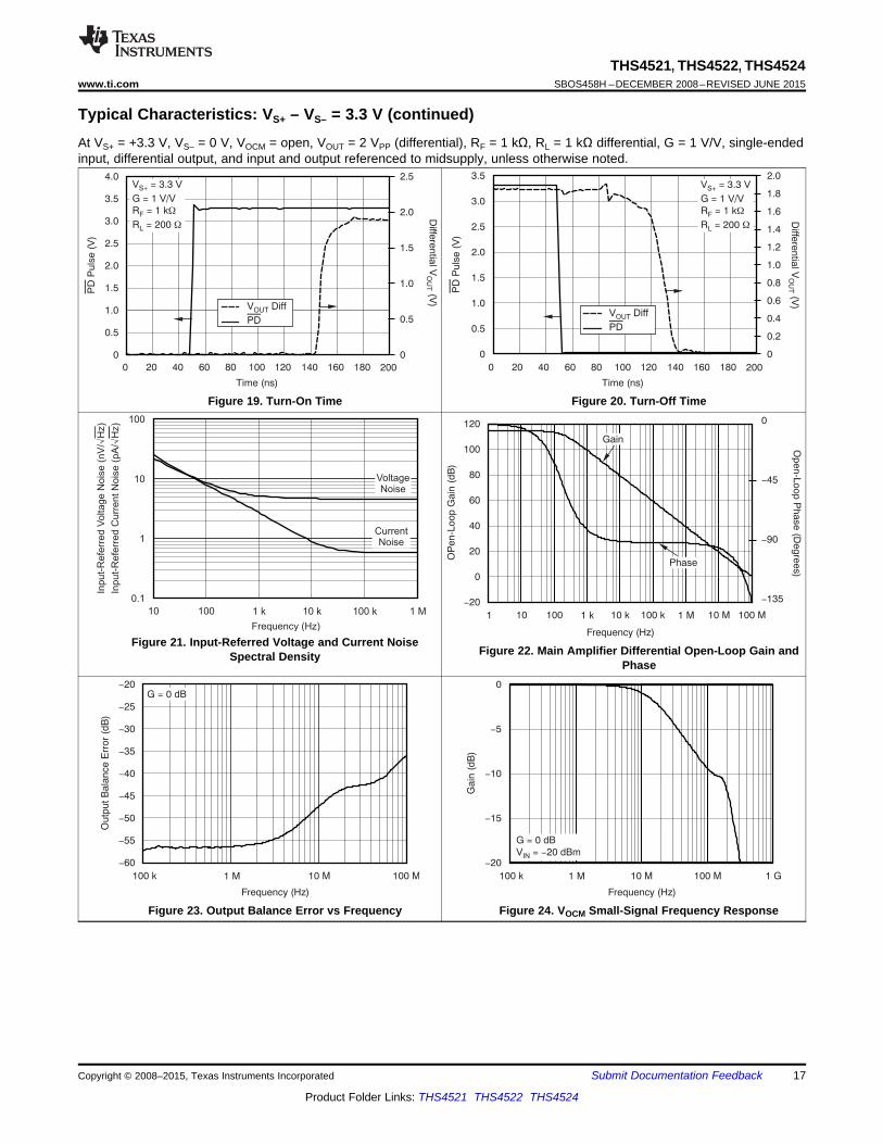
7.8 Typical Characteristics: VS+ – VS– = 3.3 VAt VS+ = +3.3 V, VS– = 0 V, VOCM = open, VOUT = 2 VPP (differential), RF = 1 kΩ, RL = 1 kΩ differential, G = 1 V/V, single-endedinput, differential output, and input and output referenced to midsupply, unless otherwise noted.
Figure 1. Small-Signal Frequency Response Figure 2. Large-Signal Frequency Response
Figure 3. Large- and Small-Signal Pulse Response Figure 4. Slew Rate vs VOUT
Figure 5. Overdrive Recovery Figure 6. 10-kHz Output Spectrum On AP Analyzer
14 Submit Documentation Feedback Copyright © 2008–2015, Texas Instruments Incorporated
Product Folder Links: THS4521 THS4522 THS4524

-30
40
50
60
70
80
90
100
-
-
-
-
-
-
-
Harm
onic
Dis
tort
ion (
dB
c)
Second
Harmonic
Third
Harmonic
V = 3.3 V
G = 1 V/V
R = 1 k
R = 1 k
f = 1 MHz
S+
F
L
PP
W
W
V = 2.0 VOUT
0 0.5 1.0 1.5 2.0 2.5 3.0
V (V)OCM
-10
20
30
40
50
60
70
80
90
100
110
-
-
-
-
-
-
-
-
-
-
Inte
rmo
du
latio
n D
isto
rtio
n (
dB
c)
1 10 100
Frequency (MHz)
Second
Intermodulation
Third
Intermodulation
V = 3.3 V
G = 1 V/V
R = 1 k
R = 1 k
S+
F
L
PP
W
W
V = 2.0 VOUT
envelope
-
-
-
-
-
-
70
75
80
85
90
95
100-
Harm
onic
Dis
tort
ion (
dB
c)
1 2 3 4 5 6 7 8 9 10
Gain (V/V)
Second
Harmonic
Third
Harmonic
V = 3.3 V
R = 1 k
R = 1 k
f = 1 MHz
S+
F
L
PP
W
W
V = 2.0 VOUT
-70
75
80
85
90
95
100
-
-
-
-
-
-
Harm
onic
Dis
tort
ion (
dB
c)
0 100 200 300 400 500 600 800 900 1 k
Load ( )W
Second
Harmonic
Third
Harmonic
V = 3.3 V
G = 1 V/V
R = 1 k
f = 1 MHz
S+
F
PP
W
V = 2.0 VOUT
-10
20
30
40
50
60
70
80
90
100
110
-
-
-
-
-
-
-
-
-
-
Harm
onic
Dis
tort
ion (
dB
c)
1 10 100
Frequency (MHz)
Second
Harmonic
Third
Harmonic
V = 3.3 V
G = 1 V/V
R = 1 k
R = 1 k
S+
F
L
W
W
V = 2.0 VOUT PP
-50
55
60
65
70
75
80
85
90
95
100
-
-
-
-
-
-
-
-
-
-
Harm
onic
Dis
tort
ion (
dB
c)
1 2 3 4 65
V (V )OUT PP
Second
Harmonic
Third
Harmonic
V = 3.3 V
G = 1 V/V
R = 1 k
R = 1 k
S+
F
L
W
W
f = 1 MHz
THS4521, THS4522, THS4524www.ti.com SBOS458H –DECEMBER 2008–REVISED JUNE 2015
Typical Characteristics: VS+ – VS– = 3.3 V (continued)At VS+ = +3.3 V, VS– = 0 V, VOCM = open, VOUT = 2 VPP (differential), RF = 1 kΩ, RL = 1 kΩ differential, G = 1 V/V, single-endedinput, differential output, and input and output referenced to midsupply, unless otherwise noted.
Figure 7. Harmonic Distortion vs Frequency Figure 8. Harmonic Distortion vs VOUT at 1 MHz
Figure 9. Harmonic Distortion vs Gain at 1 MHz Figure 10. Harmonic Distortion vs Load at 1 MHz
Figure 11. Harmonic Distortion vs VOCM at 1 MHz Figure 12. Two-Tone Intermodulation Distortion vsFrequency
Copyright © 2008–2015, Texas Instruments Incorporated Submit Documentation Feedback 15
Product Folder Links: THS4521 THS4522 THS4524
-100
105
110
115
120
125
130
135
140
-
-
-
-
-
-
-
-
Ch
an
ne
l-to
-Ch
an
ne
l C
rossta
lk (
dB
)
10 100 10 k1 k 100 k 1 M
Frequency (Hz)
V = 3.3 V
G = 1 V/V
R = 1 k
S+
F
OUT RMS
W
R = 1 kL W
Active Channel V = 1 V
110
100
90
80
70
60
50
Com
mon-M
ode R
eje
ction R
atio (
dB
)
Pow
er-
Supply
Reje
ction R
atio (
dB
)
10 k 100 k 1 M 10 M 100 M
Frequency (Hz)
V = 3.3 V
G = 1 V/V
R = 1 k
S+
F W
CMRR
+PSRR
-PSRR
5
0
5
10
15
20
25
-
-
-
-
-
Norm
aliz
ed G
ain
(dB
)
100 k 1 M 10 M 100 M 1 G
Frequency (Hz)
C = 10 pF
R = 124L
O W
C = 100 pF
R = 35.7L
O W
C = 1000 pF
R = 7.15L
O W
C = 4.7 pF
R = 150L
O W
1k
100
10
1
R(
)W
O
10 100 1000
C (pF)LOAD
3.5
3.0
2.5
2.0
1.5
1.0
0.5
0
Sin
gle
-En
de
d V
(V)
OU
T
10 100 1 k 10 k
Load Resistance ( )W
V maxOUT
V minOUT
Linear Voltage Range
V = 1.65 VOCM
100
10
1
0.1
0.01
Diffe
rential O
utp
ut Im
pedance (
)W
100 k 1 M 10 M 100 M
Frequency (Hz)
THS4521, THS4522, THS4524SBOS458H –DECEMBER 2008–REVISED JUNE 2015 www.ti.com
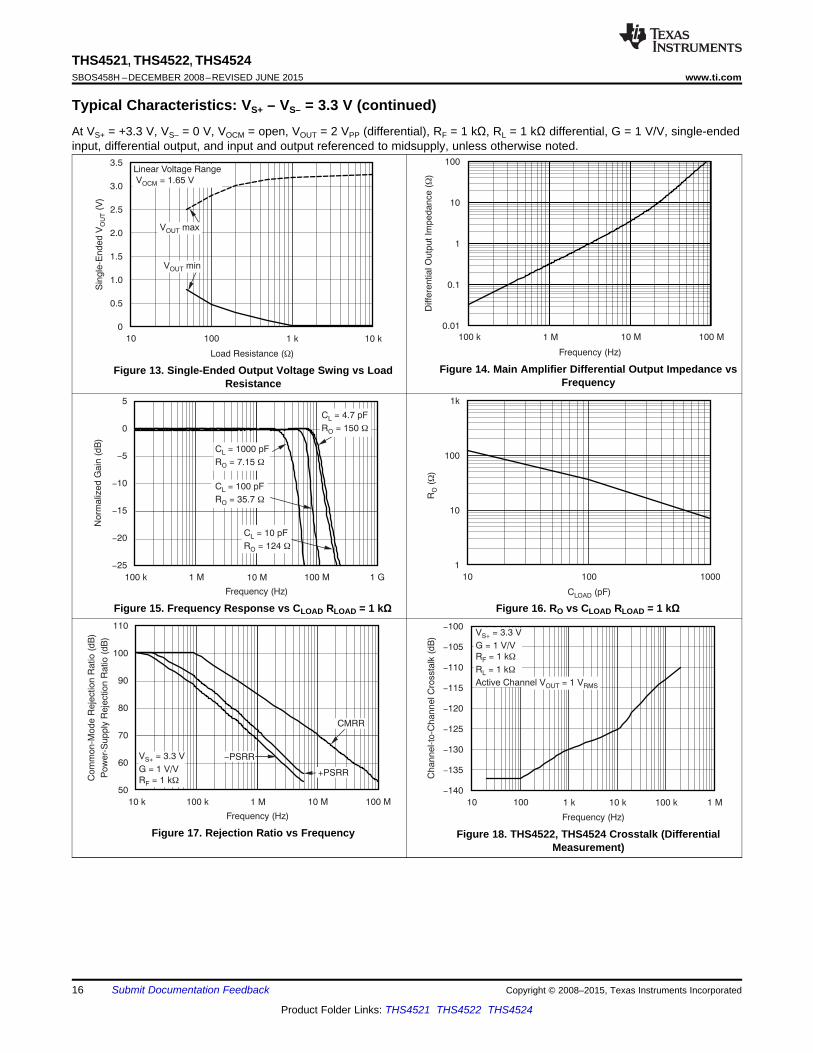
Typical Characteristics: VS+ – VS– = 3.3 V (continued)At VS+ = +3.3 V, VS– = 0 V, VOCM = open, VOUT = 2 VPP (differential), RF = 1 kΩ, RL = 1 kΩ differential, G = 1 V/V, single-endedinput, differential output, and input and output referenced to midsupply, unless otherwise noted.
Figure 14. Main Amplifier Differential Output Impedance vsFigure 13. Single-Ended Output Voltage Swing vs LoadFrequencyResistance
Figure 15. Frequency Response vs CLOAD RLOAD = 1 kΩ Figure 16. RO vs CLOAD RLOAD = 1 kΩ
Figure 17. Rejection Ratio vs Frequency Figure 18. THS4522, THS4524 Crosstalk (DifferentialMeasurement)
16 Submit Documentation Feedback Copyright © 2008–2015, Texas Instruments Incorporated
Product Folder Links: THS4521 THS4522 THS4524
-20
25
30
35
40
45
50
55
60
-
-
-
-
-
-
-
-
Ou
tpu
t B
ala
nce
Err
or
(dB
)
100 k 1 M 10 M 100 M
Frequency (Hz)
G = 0 dB0
5
10
15
20
-
-
-
-
Ga
in (
dB
)
100 k 1 M 10 M 100 M 1 G
Frequency (Hz)
G = 0 dB
V = 20 dBmIN -
120
100
80
60
40
20
0
20-
OP
en-L
oop G
ain
(dB
)
1 10 100 1 k 10 k 100 k 1 M 10 M 100 M
Frequency (Hz)
0
45
90
135-
-
-
Open-L
oop P
hase (D
egre
es)
Gain
Phase
100
10
1
0.1
Inp
ut-
Re
ferr
ed
Vo
lta
ge
No
ise
(n
V/
)
Inp
ut-
Re
ferr
ed
Cu
rre
nt
No
ise
(p
A/
)
Hz
Hz
√ √
10 100 1 k 10 k 100 k 1 M
Frequency (Hz)
CurrentNoise
VoltageNoise
4.0
3.5
3.0
2.5
2.0
1.5
1.0
0.5
0
2.5
2.0
1.5
1.0
0.5
0
PD
Puls
e (
V)
Diffe
rentia
l V(V
)O
UT
0 20 40 60 80 100 120 160 180 200
Time (ns)
V = 3.3 V
G = 1 V/V
R = 1 k
S+
F W
R = 200L W
V DiffOUT
PD
140
3.5
3.0
2.5
2.0
1.5
1.0
0.5
0
2.0
1.8
1.6
1.4
1.2
1.0
0.8
0.6
0.4
0.2
0
PD
Pu
lse
(V
)
Diffe
ren
tial V
(V)
OU
T
0 20 40 60 80 100 120 160 180 200
Time (ns)
140
V = 3.3 V
G = 1 V/V
R = 1 k
S+
F W
R = 200L W
V DiffOUT
PD
THS4521, THS4522, THS4524www.ti.com SBOS458H –DECEMBER 2008–REVISED JUNE 2015
Typical Characteristics: VS+ – VS– = 3.3 V (continued)At VS+ = +3.3 V, VS– = 0 V, VOCM = open, VOUT = 2 VPP (differential), RF = 1 kΩ, RL = 1 kΩ differential, G = 1 V/V, single-endedinput, differential output, and input and output referenced to midsupply, unless otherwise noted.
Figure 19. Turn-On Time Figure 20. Turn-Off Time
Figure 21. Input-Referred Voltage and Current NoiseFigure 22. Main Amplifier Differential Open-Loop Gain andSpectral Density
Phase
Figure 23. Output Balance Error vs Frequency Figure 24. VOCM Small-Signal Frequency Response
Copyright © 2008–2015, Texas Instruments Incorporated Submit Documentation Feedback 17
Product Folder Links: THS4521 THS4522 THS4524

2.5
2.3
2.1
1.9
1.7
1.5
1.3
1.1
0.9
0.7
0.5
VC
om
mon-M
ode V
oltage (
V)
OU
T
0 100 200 300 400
Time (ns)
V = 3.3 V
G = 1 V/V
R = 1 k
R = 1 k
S+
F
L
W
W
100 k
10 k
1 k
100
VIn
pu
t Im
pe
da
nce
()
WO
CM
100 k 1 M 10 M 100 M
Frequency (Hz)
THS4521, THS4522, THS4524SBOS458H –DECEMBER 2008–REVISED JUNE 2015 www.ti.com
Typical Characteristics: VS+ – VS– = 3.3 V (continued)At VS+ = +3.3 V, VS– = 0 V, VOCM = open, VOUT = 2 VPP (differential), RF = 1 kΩ, RL = 1 kΩ differential, G = 1 V/V, single-endedinput, differential output, and input and output referenced to midsupply, unless otherwise noted.
Figure 26. VOCM Input Impedance vs FrequencyFigure 25. VOCM Large-Signal Pulse Response
18 Submit Documentation Feedback Copyright © 2008–2015, Texas Instruments Incorporated
Product Folder Links: THS4521 THS4522 THS4524

Frequency (kHz)
Har
mon
ic D
isto
rtio
n (d
BC
)
1 10 100 1000-150
-140
-130
-120
-110
-100
-90
-80
D001
Second HarmonicThird Harmonic
6
4
2
0
2
4
6
-
-
-
3
2
1
0
1
2
3
-
-
-
Diffe
rential V
(V)
OU
T
Input V
olta
ge (V
)
0 100 200 300 400 500 600 700 800 900 1k
Time (ns)
V = 5 V
G = 2 V/V
R = 1 k
S+
F W
R = 200L W
V Diff
InputOUT
1.5
1.0
0.5
0
0.5
1.0
1.5
-
-
-
Diffe
ren
tia
l V
(V)
OU
T
0 20 40 60 80 100
Time (ns)
2-V Step
0.5-V Step
V = 5 V
G = 1 V/V
R = 1 k
R = 200
S+
F
L
W
W
800
700
600
500
400
300
200
100
0
Sle
w R
ate
(V
/s)
m
0 1 2 3 4 5 6 7
Differential V (V)OUT
V = 5 V
G = 1 V/V
R = 1 k
S+
F W
R = 200L W
Falling
Rising
6
3
0
3
6
9
12
15
18
21
24
-
-
-
-
-
-
-
-
100 k 1 M 10 M 100 M 1 G
Frequency (Hz)
No
rma
lize
d G
ain
(d
B)
G = 1 V/V
G = 2 V/V
G = 5 V/V
G = 10 V/V
V = 5.0 V
R = 1 k
V = 100 mV
S+
L
O PP
W
6
3
0
3
6
9
12
15
18
21
24
-
-
-
-
-
-
-
-
No
rma
lize
d G
ain
(d
B)
100 k 1 M 10 M 100 M 1 G
Frequency (Hz)
G = 1 V/V
G = 2 V/V
G = 5 V/V
G = 10 V/V
V = 5.0 V
R = 1 k
V = 2.0 V
S+
L
O PP
W
THS4521, THS4522, THS4524www.ti.com SBOS458H –DECEMBER 2008–REVISED JUNE 2015
7.9 Typical Characteristics: 5 VAt VS+ = +5 V, VS– = 0 V, VOCM = open, VOUT = 2 VPP (differential), RF = 1 kΩ, RL = 1 kΩ differential, G = 1 V/V, single-endedinput, differential output, and input and output referenced to midsupply, unless otherwise noted.
Figure 27. Small-Signal Frequency Response Figure 28. Large-Signal Frequency Response
Figure 29. Large- and Small-Signal Pulse Response Figure 30. Slew Rate vs VOUT
Figure 31. Overdrive Recovery Figure 32. Harmonic Distortion vs Frequency Below 1 MHz
Copyright © 2008–2015, Texas Instruments Incorporated Submit Documentation Feedback 19
Product Folder Links: THS4521 THS4522 THS4524
-70
75
80
85
90
95
100
-
-
-
-
-
-
Ha
rmo
nic
Dis
tort
ion
(d
Bc)
0 100 200 300 400 500 600 800 900 1k
Load ( )W
Second
Harmonic
Third
Harmonic
V = 5 V
G = 1 V/V
R = 1 k
f = 1 MHz
S+
F
PP
W
V = 2.0 VOUT
-30
40
50
60
70
80
90
100
-
-
-
-
-
-
-
Harm
onic
Dis
tort
ion (
dB
c)
3.0 4.0 5.0
V (V)OCM
Second
Harmonic
Third
Harmonic
V = 5 V
G = 1 V/V
R = 1 k
R = 1 k
f = 1 MHz
S+
F
L
PP
W
W
V = 2.0 VOUT
0 1.0 2.0
-
-
-
-
-
-
70
75
80
85
90
95
100-
Ha
rmo
nic
Dis
tort
ion
(d
Bc)
1 2 3 4 5 6 7 8
V (V )OUT PP
Second
Harmonic
Third
Harmonic
V = 5 V
G = 1 V/V
R = 1 k
R = 1 k
S+
F
L
W
W
f = 1 MHz
-
-
-
-
-
-
70
75
80
85
90
95
100-
Harm
onic
Dis
tort
ion (
dB
c)
1 2 3 4 5 6 7 8 9 10
Gain (V/V)
Second
Harmonic
Third
Harmonic
V = 5 V
R = 1 k
R = 1 k
f = 1 MHz
S+
F
L
PP
W
W
V = 2.0 VOUT
10
0
-10
20
30
40
50
60
70
80
90
100
110
120
130
140
-
-
-
-
-
-
-
-
-
-
-
-
-
Ma
gn
itu
de
(d
Bv)
0 5 k 10 k 15 k 20 k 25 k 30 k 35 k
Frequency (Hz)
THS4521V = 5.0 V
G = 1 V/VR = 1 k
V = 8 V
S+
F
OUT PP
Ω
-10
20
30
40
50
60
70
80
90
100
110
-
-
-
-
-
-
-
-
-
-
Harm
onic
Dis
tort
ion (
dB
c)
1 10 100
Frequency (MHz)
Second
Harmonic
Third
Harmonic
V = 5 V
G = 1 V/V
R = 1 k
R = 1 k
S+
F
L
PP
W
W
V = 2.0 VOUT
THS4521, THS4522, THS4524SBOS458H –DECEMBER 2008–REVISED JUNE 2015 www.ti.com
Typical Characteristics: 5 V (continued)At VS+ = +5 V, VS– = 0 V, VOCM = open, VOUT = 2 VPP (differential), RF = 1 kΩ, RL = 1 kΩ differential, G = 1 V/V, single-endedinput, differential output, and input and output referenced to midsupply, unless otherwise noted.
Figure 33. 10-kHz Output Spectrum On AP Analyzer at Figure 34. Harmonic Distortion vs FrequencyVOUT = 8 VPP
Figure 36. Harmonic Distortion vs Gain at 1 MHzFigure 35. Harmonic Distortion vs VOUT at 1 MHz
Figure 37. Harmonic Distortion vs Load at 1 MHz Figure 38. Harmonic Distortion vs VOCM at 1 MHz
20 Submit Documentation Feedback Copyright © 2008–2015, Texas Instruments Incorporated
Product Folder Links: THS4521 THS4522 THS4524

1k
100
10
1
R(
)W
O
10 100 1000
C (pF)LOAD
110
100
90
80
70
60
50
Com
mon-M
ode R
eje
ction R
atio (
dB
)
Pow
er-
Supply
Reje
ction R
atio (
dB
)
10 k 100 k 1 M 10 M 100 M
Frequency (Hz)
V = 5.0 V
G = 1 V/V
R = 1 k
S+
F W
CMRR
+PSRR
PSRR-
100
10
1
0.1
0.01
Diffe
rential O
utp
ut Im
pedance (
)W
100 k 1 M 10 M 100 M
Frequency (Hz)
5
0
5
10
15
20
25
-
-
-
-
-
Norm
aliz
ed G
ain
(dB
)
100 k 1 M 10 M 100 M 1 G
Frequency (Hz)
C = 10 pF
R = 124L
O W
C = 100 pF
R = 35.7L
O W
C = 1000 pF
R = 7.15L
O W
C = 4.7 pF
R = 150L
O W
-10
20
30
40
50
60
70
80
90
100
110
-
-
-
-
-
-
-
-
-
-
Inte
rmo
du
latio
n D
isto
rtio
n (
dB
c)
1 10 100
Frequency (MHz)
Second
Intermodulation
Third
Intermodulation
V = 5 V
G = 1 V/V
R = 1 k
R = 1 k
S+
F
L
PP
W
W
V = 2.0 VOUT
envelope
5.0
4.5
4.0
3.5
3.0
2.5
2.0
1.5
1.0
0.5
0
Sin
gle
-Ended V
(V)
OU
T
10 100 1 k 10 k
Load Resistance (W)
V maxOUT
V minOUT
Linear Output Voltage RangeV = 2.5 VOCM
THS4521, THS4522, THS4524www.ti.com SBOS458H –DECEMBER 2008–REVISED JUNE 2015
Typical Characteristics: 5 V (continued)At VS+ = +5 V, VS– = 0 V, VOCM = open, VOUT = 2 VPP (differential), RF = 1 kΩ, RL = 1 kΩ differential, G = 1 V/V, single-endedinput, differential output, and input and output referenced to midsupply, unless otherwise noted.
Figure 40. Single-Ended Output Voltage Swing vsFigure 39. Two-Tone Intermodulation Distortion vsDifferential Load ResistanceFrequency
Figure 41. Main Amplifier Differential Output Impedance vs Figure 42. Frequency Response vs CLOAD RLOAD = 1 kΩFrequency
Figure 43. RO vs CLOAD RLOAD = 1 kΩ Figure 44. Rejection Ratio vs Frequency
Copyright © 2008–2015, Texas Instruments Incorporated Submit Documentation Feedback 21
Product Folder Links: THS4521 THS4522 THS4524

120
100
80
60
40
20
0
20-
OP
en-L
oop G
ain
(dB
)
1 10 100 1 k 10 k 100 k 1 M 10 M 100 M
Frequency (Hz)
0
45
90
135
-
-
-
Open-L
oop P
hase (D
egre
es)
Gain
Phase
-20
25
30
35
40
45
50
55
60
-
-
-
-
-
-
-
-
Ou
tpu
t B
ala
nce
Err
or
(dB
)
100 k 1 M 10 M 100 M
Frequency (Hz)
G = 0 dB
3.5
3.0
2.5
2.0
1.5
1.0
0.5
0
2.0
1.8
1.6
1.4
1.2
1.0
0.8
0.6
0.4
0.2
0
PD
Pu
lse
(V
)
Diffe
ren
tial V
(V)
OU
T
0 20 40 60 80 100 120 160 180 200
Time (ns)
140
V = 5 V
G = 1 V/V
R = 1 k
S+
F W
R = 200L W
V DiffOUT
PD
100
10
1
0.1
Inp
ut-
Re
ferr
ed
Vo
lta
ge
No
ise
(n
V/
)
Inp
ut-
Re
ferr
ed
Cu
rre
nt
No
ise
(p
A/
)
Hz
Hz
√ √
10 100 1 k 10 k 100 k 1 M
Frequency (Hz)
CurrentNoise
VoltageNoise
-100
105
110
115
120
125
130
135
140
-
-
-
-
-
-
-
-
Ch
an
ne
l-to
-Ch
an
ne
l C
rossta
lk (
dB
)
10 100 10 k1 k 100 k 1 M
Frequency (Hz)
V = 5 V
G = 1 V/V
R = 1 k
S+
F
OUT RMS
W
R = 1 kL W
Active Channel V = 1 V
4.0
3.5
3.0
2.5
2.0
1.5
1.0
0.5
0
2.5
2.0
1.5
1.0
0.5
0
PD
Puls
e (
V)
Diffe
rentia
l V(V
)O
UT
0 20 40 60 80 100 120 160 180 200
Time (ns)
V = 5 V
G = 1 V/V
R = 1 k
S+
F W
R = 200L W
V DiffOUT
PD
140
THS4521, THS4522, THS4524SBOS458H –DECEMBER 2008–REVISED JUNE 2015 www.ti.com
Typical Characteristics: 5 V (continued)At VS+ = +5 V, VS– = 0 V, VOCM = open, VOUT = 2 VPP (differential), RF = 1 kΩ, RL = 1 kΩ differential, G = 1 V/V, single-endedinput, differential output, and input and output referenced to midsupply, unless otherwise noted.
Figure 46. Turn-On TimeFigure 45. THS4522, THS4524 Crosstalk (MeasuredDifferentially)
Figure 48. Input-Referred Voltage and Current NoiseFigure 47. Turn-Off TimeSpectral Density
Figure 50. Output Balance Error vs FrequencyFigure 49. Main Amplifier Differential Open-Loop Gain andPhase
22 Submit Documentation Feedback Copyright © 2008–2015, Texas Instruments Incorporated
Product Folder Links: THS4521 THS4522 THS4524

100 k
10 k
1 k
100
VIn
pu
t Im
pe
da
nce
()
WO
CM
100 k 1 M 10 M 100 M
Frequency (Hz)
3.5
3.3
3.1
2.9
2.7
2.5
2.3
2.1
1.9
1.7
1.5
VC
om
mon-M
ode V
oltage (
V)
OU
T
0 100 200 300 400
Time (ns)
V = 5.0 V
G = 1 V/V
R = 1 k
R = 1 k
S+
F
L
W
W
0
5
10
15
20
-
-
-
-
Ga
in (
dB
)
100 k 1 M 10 M 100 M 1 G
Frequency (Hz)
G = 0 dB
V = 20 dBmIN -
THS4521, THS4522, THS4524www.ti.com SBOS458H –DECEMBER 2008–REVISED JUNE 2015
Typical Characteristics: 5 V (continued)At VS+ = +5 V, VS– = 0 V, VOCM = open, VOUT = 2 VPP (differential), RF = 1 kΩ, RL = 1 kΩ differential, G = 1 V/V, single-endedinput, differential output, and input and output referenced to midsupply, unless otherwise noted.
Figure 51. VOCM Small-Signal Frequency Response Figure 52. VOCM Large-Signal Pulse Response
Figure 53. VOCM Input Impedance vs Frequency
Copyright © 2008–2015, Texas Instruments Incorporated Submit Documentation Feedback 23
Product Folder Links: THS4521 THS4522 THS4524

THS4521, THS4522, THS4524SBOS458H –DECEMBER 2008–REVISED JUNE 2015 www.ti.com
8 Detailed Description
8.1 OverviewThe THS4521, THS4522, and THS4524 family is tested with the test circuits shown in this section; all circuits arebuilt using the available THS4521 evaluation module (EVM). For simplicity, power-supply decoupling is notshown; see the layout in the Typical Applications section for recommendations. Depending on the test conditions,component values change in accordance with Table 4 and Table 5, or as otherwise noted. In some cases thesignal generators used are ac-coupled and in others they dc-coupled 50-Ω sources. To balance the amplifierwhen ac-coupled, a 0.22-μF capacitor and 49.9-Ω resistor to ground are inserted across RIT on the alternateinput; when dc-coupled, only the 49.9-Ω resistor to ground is added across RIT. A split power supply is used toease the interface to common test equipment, but the amplifier can be operated in a single-supply configurationas described in the Typical Applications section with no impact on performance. Also, for most of the tests,except as noted, the devices are tested with single-ended inputs and a transformer on the output to convert thedifferential output to single-ended because common lab test equipment has single-ended inputs and outputs.Similar or better performance can be expected with differential inputs and outputs.
As a result of the voltage divider on the output formed by the load component values, the amplifier output isattenuated. The Atten column in Table 5 shows the attenuation expected from the resistor divider. When using atransformer at the output (as shown in Figure 55), the signal sees slightly more loss because of transformer andline loss; these numbers are approximate.
Table 4. Gain Component Values for Single-Ended Input (see Figure 54)Gain RF RG RIT
1 V/V 1 kΩ 1 kΩ 52.3 Ω
2 V/V 1 kΩ 487 Ω 53.6 Ω
5 V/V 1 kΩ 191 Ω 59.0 Ω
10 V/V 1 kΩ 86.6 Ω 69.8 Ω
1. Gain setting includes 50-Ω source impedance. Components are chosen to achieve gain and 50-Ω inputtermination.
Table 5. Load Component Values For 1:1 Differential To Single-Ended Output Transformer (SeeFigure 55)
RL RO ROT Atten
100 Ω 24.9 Ω Open 6 dB
200 Ω 86.6 Ω 69.8 Ω 16.8 dB
499 Ω 237 Ω 56.2 Ω 25.5 dB
1 kΩ 487 Ω 52.3 Ω 31.8 dB
1. Total load includes 50-Ω termination by the test equipment. Components are chosen to achieve load and 50-Ω line termination through a 1:1 transformer.
24 Submit Documentation Feedback Copyright © 2008–2015, Texas Instruments Incorporated
Product Folder Links: THS4521 THS4522 THS4524

THS452x
RG
RGRIT
RIT
24.9 W953 W
1 kW
1 kW
49.9 W
24.9 W
VOCM
VIN+
PDMeasure with
Differential
Probe
Across ROT
Installed to
Balance
Amplifier
Calibrated
Differential
Probe
Across
RIT
Open
Open
From
50-
Source
W
VS+
VS-
0.22 Fm
0.22 Fm
Vs+
IN–
+
–
High-Aol
Differential I/O
Amplifier
IN+
FB+
275 kΩ
5 kΩ
5 kΩ
OUT+
OUT–
+
–
FB–
+
–Vcm
Error
AmplifierVocm
Vs+
275 kΩ
PD CMOS
Buffer
Vs–
(RGT Package)
(RGT Package)
THS4521, THS4522, THS4524www.ti.com SBOS458H –DECEMBER 2008–REVISED JUNE 2015
8.2 Functional Block Diagram
8.3 Feature Description
8.3.1 Frequency ResponseThe circuit shown in Figure 54 is used to measure the frequency response of the circuit.
A network analyzer is used as the signal source and the measurement device. The output impedance of thenetwork analyzer is dc-coupled and is 50 Ω. RIT and RG are chosen to impedance-match to 50 Ω and maintainthe proper gain. To balance the amplifier, a 49.9-Ω resistor to ground is inserted across RIT on the alternateinput.
The output is probed using a Tektronix high-impedance differential probe across the 953-Ω resistor and referredto the amplifier output by adding back the 0.42-dB because of the voltage divider on the output.
Figure 54. Frequency Response Test Circuit
Copyright © 2008–2015, Texas Instruments Incorporated Submit Documentation Feedback 25
Product Folder Links: THS4521 THS4522 THS4524

THS452x
RG
RGRIT
RIT
49.9 W
1 kW
1 kW
49.9 W
49.9 W
VOCM
VIN+
PD
Installed to
Balance
Amplifier
Open
Open
From
50-
Source
W
VOUT-
VOUT+To Oscilloscope
with 50- InputW
VS+
VS-
0.22 Fm
0.22 Fm
THS452x
RG RF
RO
ROROT
RGRF
RIT
RIT
VOCM
VOUT
PD
Installed to
Balance
Amplifier
Open
Open
1:1
From
50-
Source
W
VIN+
0.22 Fm
0.22 Fm
0.22 Fm
To 50-
Test
Equipment
W
VS-
VS+
49.9 W
THS4521, THS4522, THS4524SBOS458H –DECEMBER 2008–REVISED JUNE 2015 www.ti.com
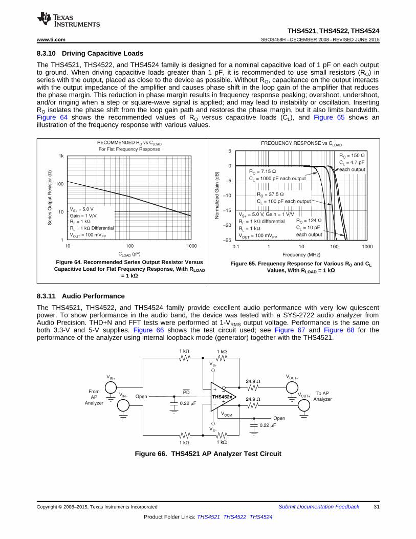
Feature Description (continued)8.3.2 DistortionThe circuit shown in Figure 55 is used to measure harmonic and intermodulation distortion of the amplifier.
A signal generator is used as the signal source and the output is measured with a Rhode and Schwarz spectrumanalyzer. The output impedance of the HP signal generator is ac-coupled and is 50 Ω. RIT and RG are chosen toimpedance match to 50 Ω and maintain the proper gain. To balance the amplifier, a 0.22-μF capacitor and 49.9-Ω resistor to ground are inserted across RIT on the alternate input.
A low-pass filter is inserted in series with the input to reduce harmonics generated at the signal source. The levelof the fundamental is measured and then a notch filter is inserted at the output to reduce the fundamental so itdoes not generate distortion in the input of the spectrum analyzer.
The transformer used in the output to convert the signal from differential to single-ended is an ADT1–1WT. Itlimits the frequency response of the circuit so that measurements cannot be made below approximately 1 MHz.
Figure 55. Distortion Test Circuit
8.3.3 Slew Rate, Transient Response, Settling Time, Output Impedance, Overdrive, Output Voltage, andTurn-On/Turn-Off Time
The circuit shown in Figure 56 is used to measure slew rate, transient response, settling time, output impedance,overdrive recovery, output voltage swing, and ampliifer turn-on/turn-off time. Turn-on and turn-off time aremeasured with the same circuit modified for 50-Ω input impedance on the PD input by replacing the 0.22-μFcapacitor with a 49.9-Ω resistor. For output impedance, the signal is injected at VOUT with VIN open; the dropacross the 2x 49.9-Ω resistors is then used to calculate the impedance seen looking into the amplifier output.
Figure 56. Slew Rate, Transient Response, Settling Time, Output Impedance, Overdrive Recovery, VOUTSwing, and Turn-On/Turn-Off Test Circuit
26 Submit Documentation Feedback Copyright © 2008–2015, Texas Instruments Incorporated
Product Folder Links: THS4521 THS4522 THS4524

THS452x24.9 W
953 W
1 kW1 kW
1 kW1 kW52.3 W
52.3 W
24.9 W
VOCM
PDMeasure with
Differential
Probe
Across ROT
Open
Open
Open
Open
Network
Analyzer
Power
Supply
Calibrated Differential
Probe
Across
VS+ and GND
VS+
VS-
0.22 Fm
0.22 Fm
THS452x24.9 W
953 W
1 kW1 kW
1 kW1 kW
52.3 W
24.9 W
VOCM
VIN+
PD Measure with
Differential
ProbeCalibrated
Differential
ProbeOpen
Open
From
Network
Analyzer VS+
VS-
0.22 Fm
0.22 Fm
THS4521, THS4522, THS4524www.ti.com SBOS458H –DECEMBER 2008–REVISED JUNE 2015
Feature Description (continued)8.3.4 Common-Mode and Power-Supply RejectionThe circuit shown in Figure 57 is used to measure the CMRR. The signal from the network analyzer is appliedcommon-mode to the input. Figure 58 is used to measure the PSRR of VS+ and VS–. The power supply undertest is applied to the network analyzer dc offset input. For both CMRR and PSRR, the output is probed using aTektronix high-impedance differential probe across the 953-Ω resistor and referred to the amplifier output byadding back the 0.42-dB as a result of the voltage divider on the output. For these tests, the resistors arematched for best results.
Figure 57. CMRR Test Circuit
Figure 58. PSRR Test Circuit
Copyright © 2008–2015, Texas Instruments Incorporated Submit Documentation Feedback 27
Product Folder Links: THS4521 THS4522 THS4524

THS452x499 W
1 kW1 kW
1 kW1 kW52.3 W
52.3 W
499 W
VOCM
PDOpen
Open
Open
49.9 W
49.9 W
Step
Input
To Oscilloscope
50- InputW
VS+
VS-
0.22 Fm
THS452x
1 kW1 kW
VOCM
PDOpen
Open
Open
MeasurementPoint for Bandwidth
MeasurementPoint for ZIN
CalibratedDifferential
ProbeAcross49.9
ResistorΩ
RCM FromNetworkAnalyzer
1 kΩ 1 kΩ
49.9 Ω
49.9 Ω
49.9 Ω
499 Ω
499 Ω
VS+
0.22 Fμ
VS
THS4521, THS4522, THS4524SBOS458H –DECEMBER 2008–REVISED JUNE 2015 www.ti.com
Feature Description (continued)8.3.5 VOCM InputThe circuit illustrated in Figure 59 is used to measure the frequency response and skew rate of the VOCM input.Frequency response is measured using a Tektronix high-impedance differential probe, withRCM = 0 Ω at the common point of VOUT+ and VOUT–, formed at the summing junction of the two matched 499-Ωresistors, with respect to ground. The input impedance is measured using a Tektronix high-impedance differentialprobe at the VOCM input with RCM = 10 kΩ and the drop across the 10-kΩ resistor is used to calculate theimpedance seen looking into the amplifier VOCM input.
The circuit shown in Figure 60 measures the transient response and slew rate of the VOCM input. A 1-V step inputis applied to the VOCM input and the output is measured using a 50-Ω oscilloscope input referenced back to theamplifier output.
Figure 59. VOCM Input Test Circuit
Figure 60. VOCM Transient Response and Slew Rate Test Circuit
28 Submit Documentation Feedback Copyright © 2008–2015, Texas Instruments Incorporated
Product Folder Links: THS4521 THS4522 THS4524
THS452x
RG RF
RO
RO
RGRF
RIT
RIT
VS-
VOCM
VIN+
PD
Optional;
installed to
balance
impedance seen
at VIN+
VOCM Control
PD Control
VOUT-
VOUT+
VS+
0.22 Fm
0.22 Fm
THS4521, THS4522, THS4524www.ti.com SBOS458H –DECEMBER 2008–REVISED JUNE 2015
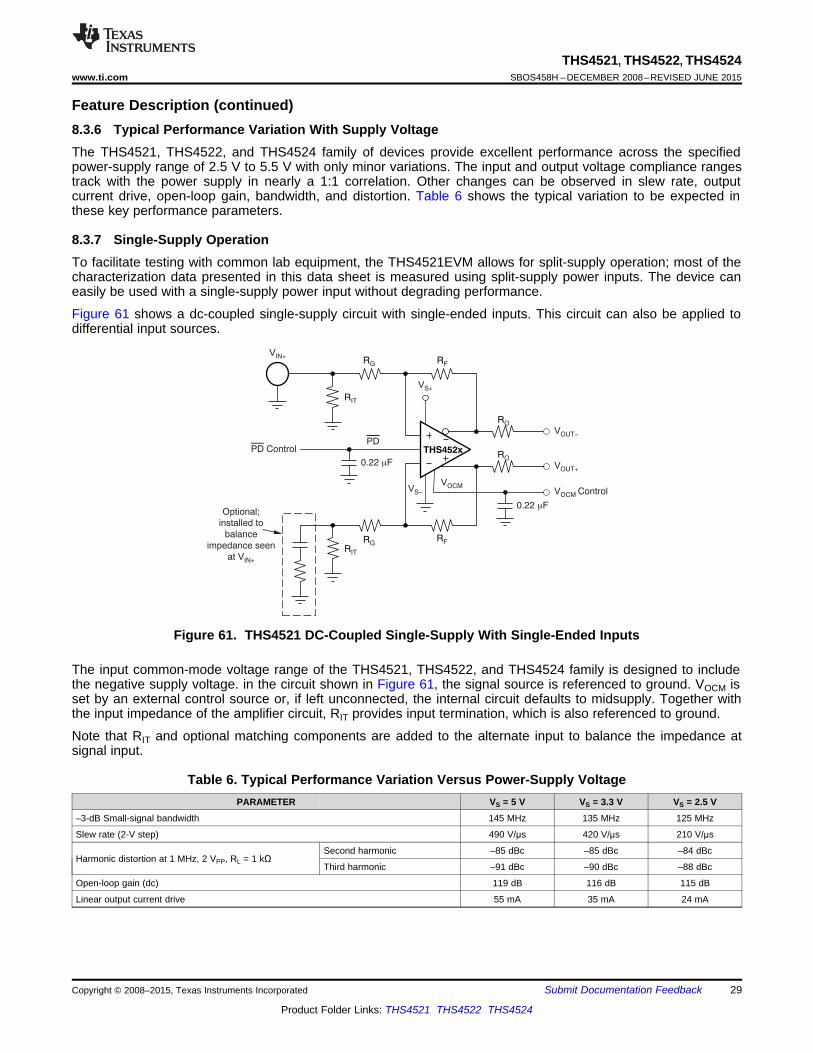
Feature Description (continued)8.3.6 Typical Performance Variation With Supply VoltageThe THS4521, THS4522, and THS4524 family of devices provide excellent performance across the specifiedpower-supply range of 2.5 V to 5.5 V with only minor variations. The input and output voltage compliance rangestrack with the power supply in nearly a 1:1 correlation. Other changes can be observed in slew rate, outputcurrent drive, open-loop gain, bandwidth, and distortion. Table 6 shows the typical variation to be expected inthese key performance parameters.
8.3.7 Single-Supply OperationTo facilitate testing with common lab equipment, the THS4521EVM allows for split-supply operation; most of thecharacterization data presented in this data sheet is measured using split-supply power inputs. The device caneasily be used with a single-supply power input without degrading performance.
Figure 61 shows a dc-coupled single-supply circuit with single-ended inputs. This circuit can also be applied todifferential input sources.
Figure 61. THS4521 DC-Coupled Single-Supply With Single-Ended Inputs
The input common-mode voltage range of the THS4521, THS4522, and THS4524 family is designed to includethe negative supply voltage. in the circuit shown in Figure 61, the signal source is referenced to ground. VOCM isset by an external control source or, if left unconnected, the internal circuit defaults to midsupply. Together withthe input impedance of the amplifier circuit, RIT provides input termination, which is also referenced to ground.
Note that RIT and optional matching components are added to the alternate input to balance the impedance atsignal input.
Table 6. Typical Performance Variation Versus Power-Supply VoltagePARAMETER VS = 5 V VS = 3.3 V VS = 2.5 V
–3-dB Small-signal bandwidth 145 MHz 135 MHz 125 MHz
Slew rate (2-V step) 490 V/μs 420 V/μs 210 V/μs
Second harmonic –85 dBc –85 dBc –84 dBcHarmonic distortion at 1 MHz, 2 VPP, RL = 1 kΩ
Third harmonic –91 dBc –90 dBc –88 dBc
Open-loop gain (dc) 119 dB 116 dB 115 dB
Linear output current drive 55 mA 35 mA 24 mA
Copyright © 2008–2015, Texas Instruments Incorporated Submit Documentation Feedback 29
Product Folder Links: THS4521 THS4522 THS4524

6
3
0
3
6
9
12
15
18
21
24
-
-
-
-
-
-
-
-
0.1 1 10 100 1000
Frequency (MHz)
SMALL-SIGNAL FREQUENCY RESPONSE
Device and Package Option Comparison
V = 5.0 V
Gain = 1 V/VS+
R = 1 k
R = 1 kF
L
W
W
THS4522,
THS4524
THS4521
MSOP
THS4521
SOIC
Sig
nal G
ain
(dB
)6
3
0
3
6
9
12
15
18
21
24
–
–
–
–
–
–
–
–
0.1 1 10 100 1000
Frequency (MHz)
SMALL-SIGNAL FREQUENCY RESPONSE
Gain = 1, R = R = R = 1 k and 10 kF G L Ω Ω
1 kΩ
10 kΩ
V = 5.0 V
V = 100 mV
Gain = 1 V/V
S+
O PP
Sig
nal G
ain
(d
B)
THS4521, THS4522, THS4524SBOS458H –DECEMBER 2008–REVISED JUNE 2015 www.ti.com
8.3.8 Low-Power Applications and the Effects of Resistor Values on BandwidthFor low-power operation, it may be necessary to increase the gain setting resistors values to limit currentconsumption and not load the source. Using larger value resistors lowers the bandwidth of the THS4521,THS4522, and THS4524 family as a result of the interactions between the resistors, the device parasiticcapacitance, and printed circuit board (PCB) parasitic capacitance. Figure 62 shows the small-signal frequencyresponse with 1-kΩ and 10-kΩ resistors for RF, RG, and RL (impedance is assumed to typically increase for allthree resistors in low-power applications).
Figure 62. THS4521 Frequency Response With Various Gain Setting and Load Resistor Values
8.3.9 Frequency Response Variation due to Package OptionsUsers can see variations in the small-signal (VOUT = 100 mVPP) frequency response between the availablepackage options for the THS4521, THS4522, and THS4524 family as a result of parasitic elements associatedwith each package and board layout changes. Figure 63 shows the variance measured in the lab; this variance isto be expected even when using a good layout.
Figure 63. Small-Signal Frequency Response: Package Variations
30 Submit Documentation Feedback Copyright © 2008–2015, Texas Instruments Incorporated
Product Folder Links: THS4521 THS4522 THS4524
THS452x24.9 W
1 kW1 kW
1 kW1 kW
24.9 W
VOCM
PD
Open
OpenFrom
AP
Analyzer
VOUT+
VIN+
To AP
Analyzer
VS+
VIN-
VS-
0.22 Fm
0.22 Fm
VOUT-
0.1 1 10 100 1000
Frequency (MHz)
5
0
5
10
15
20
25
-
-
-
-
-
Norm
aliz
ed G
ain
(dB
)
FREQUENCY RESPONSE vs CLOAD
R = 124
C = 10 pF
each output
WO
L
R = 37.5
C = 100 pF each output
WO
L
R = 7.15
C = 1000 pF each output
WO
L
R = 150
C = 4.7 pF
each output
WO
L
V = 5.0 V, Gain = 1 V/VS+
PP
R = 1 k differential
R = 1 k
V = 100 mV
F
L
OUT
W
W
1k
100
10
1
10 100 1000
C (pF)LOAD
Se
rie
s O
utp
ut
Re
sis
tor
()
W
RECOMMENDED R vs C
For Flat Frequency ResponseO LOAD
V = 5.0 V
Gain = 1 V/VS+
PP
R = 1 k
R = 1 k Differential
V = 100 mV
F
L
OUT
W
W
THS4521, THS4522, THS4524www.ti.com SBOS458H –DECEMBER 2008–REVISED JUNE 2015
8.3.10 Driving Capacitive LoadsThe THS4521, THS4522, and THS4524 family is designed for a nominal capacitive load of 1 pF on each outputto ground. When driving capacitive loads greater than 1 pF, it is recommended to use small resistors (RO) inseries with the output, placed as close to the device as possible. Without RO, capacitance on the output interactswith the output impedance of the amplifier and causes phase shift in the loop gain of the amplifier that reducesthe phase margin. This reduction in phase margin results in frequency response peaking; overshoot, undershoot,and/or ringing when a step or square-wave signal is applied; and may lead to instability or oscillation. InsertingRO isolates the phase shift from the loop gain path and restores the phase margin, but it also limits bandwidth.Figure 64 shows the recommended values of RO versus capacitive loads (CL), and Figure 65 shows anillustration of the frequency response with various values.
Figure 64. Recommended Series Output Resistor Versus Figure 65. Frequency Response for Various RO and CLCapacitive Load for Flat Frequency Response, With RLOAD Values, With RLOAD = 1 kΩ
= 1 kΩ
8.3.11 Audio PerformanceThe THS4521, THS4522, and THS4524 family provide excellent audio performance with very low quiescentpower. To show performance in the audio band, the device was tested with a SYS-2722 audio analyzer fromAudio Precision. THD+N and FFT tests were performed at 1-VRMS output voltage. Performance is the same onboth 3.3-V and 5-V supplies. Figure 66 shows the test circuit used; see Figure 67 and Figure 68 for theperformance of the analyzer using internal loopback mode (generator) together with the THS4521.
Figure 66. THS4521 AP Analyzer Test Circuit
Copyright © 2008–2015, Texas Instruments Incorporated Submit Documentation Feedback 31
Product Folder Links: THS4521 THS4522 THS4524

-95
97
99
101
103
-
-
-
-
-
-
-
-
-
-
105
107
109
111
113
115
TH
D+
N (
dB
)
10 100 1 k 10 k 100 k
Frequency (Hz)
TOTAL HARMONIC DISTORTION + NOISE
vs FREQUENCY (No Weighting)
10
0
10
20
30
40
50
60
70
80
90
100
110
120
130
140
-
-
-
-
-
-
-
-
-
-
-
-
-
-
Ma
gn
itu
de
(d
Bv)
0 5 k 10 k 15 k 20 k 25 k 30 k 35 k
Frequency (Hz)
Generator
THS4521
V = 5.0 V
G = 1 V/V
R = 1 k
V = 1 V
S+
F
OUT RMS
W
10-kHz OUTPUT SPECTRUM
THS4521 on AP Analyzer
-50
60
70
80
90
100
110
120
-
-
-
-
-
-
-
TH
D+
N (
dB
v)
0 5 10 15 20
Frequency (kHz)
TOTAL HARMONIC DISTORTION + NOISE
THS4521 Measured on AP Analyzer
THS4521
Signal Generator
THS4521, THS4522, THS4524SBOS458H –DECEMBER 2008–REVISED JUNE 2015 www.ti.com
Note that the harmonic distortion performance is very close to the same with and without the device meaning theTHS4521 performance is actually much better than can be directly measured by this method. The actual deviceperformance can be estimated by placing the device in a large noise gain and using the reduction in loop gaincorrection. The THS4521 is placed in a noise gain of 101 by adding a 10-Ω resistor directly across the inputterminals of the circuit shown in Figure 66. This test was performed using the AP instrument as both the signalsource and the analyzer. The second-order harmonic distortion at 1 kHz is estimated to be –122 dBc with VO =1VRMS; third-order harmonic distortion is estimated to be –141 dBc. The third-order harmonic distortion resultmatches exactly with design simulations, but the second-order harmonic distortion is about 10 dB worse. Thisresult is not unexpected because second-order harmonic distortion performance with a differential signaldepends heavily on cancellation as a result of the differential nature of the signal, which depends on boardlayout, bypass capacitors, external cabling, and so forth. Note that the circuit of Figure 66 is also used tomeasure crosstalk between channels.
The THS4521 shows even better THD+N performance when driving higher amplitude output, such as 5 VPP thatis more typical when driving an ADC. To show performance with an extended frequency range, higher gain, andhigher amplitude, the device was tested with 5 VPP up to 80 kHz with the AP. Figure 69 shows the resultingTHD+N graph with no weighting.
Figure 67. THS4521 1-VRMS 20-Hz to 20-kHz Thd+N Figure 68. THS4521 1-VRMS 10-kHz FFT Plot
Figure 69. Thd+N (No Weighting) on Ap, 80-kHz Bandwidth at G = 1 With 5-VPP Output
32 Submit Documentation Feedback Copyright © 2008–2015, Texas Instruments Incorporated
Product Folder Links: THS4521 THS4522 THS4524

Vo
lta
ge
(V
)
0 50 100 150 200
Time (ms)
PD
5.0
4.5
4.0
3.5
3.0
2.5
2.0
1.5
1.0
0.5
0
Outputs
PD ENABLE POP PERFORMANCE
Vo
lta
ge
(V
)
0 50 100 150 200
Time (ms)
PD
5.0
4.5
4.0
3.5
3.0
2.5
2.0
1.5
1.0
0.5
0
Outputs
PD DISABLE POP PERFORMANCE
Vo
lta
ge
(V
)
0 50 100 150 200
Time (ms)
Power
Supply
5.0
4.5
4.0
3.5
3.0
2.5
2.0
1.5
1.0
0.5
0
Outputs
POWER-SUPPLY TURN-ON POP PERFORMANCE
Vo
lta
ge
(V
)0 50 100 150 200
Time (ms)
Power
Supply
5.0
4.5
4.0
3.5
3.0
2.5
2.0
1.5
1.0
0.5
0
Outputs
POWER-SUPPLY TURN-OFF POP PERFORMANCE
THS4521, THS4522, THS4524www.ti.com SBOS458H –DECEMBER 2008–REVISED JUNE 2015
8.3.12 Audio On/Off Pop PerformanceThe THS4521 was tested to show on and off pop performance by connecting a speaker between the differentialoutputs and switching the power supply on and off, and also by using the PD function of the THS4521. Testingwas done with and without tones. During these tests, no audible pop could be heard.
With no tone input, Figure 70 shows the pop performance when switching power on to the THS4521 andFigure 71 shows the device performance when turning the power off. The transients during power on and offillustrate that no audible pop should be heard
Figure 70. THS4521 Power-Supply Turn-On Pop Figure 71. THS4521 Power-Supply Turn-Off PopPerformance Performance
With no tone input, Figure 72 shows the pop performance using the PD pin to enable the THS4521, andFigure 73 shows performance using the PD pin to disable the device. Again, the transients during power on andoff show that no audible pop should be heard. It should also be noted that the turn on/off times are faster usingthe PD pin technique.
Figure 72. THS4521 PD Pin Enable Pop Performance Figure 73. THS4521 PD Pin Disable Pop Performance
The power on/off pop performance of the THS4521, whether by switching the power supply or when using thepower-down function built into the chip, shows that no special design should be required to prevent an audiblepop.
Copyright © 2008–2015, Texas Instruments Incorporated Submit Documentation Feedback 33
Product Folder Links: THS4521 THS4522 THS4524

THS4521, THS4522, THS4524SBOS458H –DECEMBER 2008–REVISED JUNE 2015 www.ti.com
8.4 Device Functional ModesThis wideband FDA requires external resistors for correct signal-path operation. When configured for the desiredinput impedance and gain setting with these external resistors, the amplifier can be either on with the PD pinasserted to a voltage greater than VS– + 1.7 V, or turned off by asserting PD low. Disabling the amplifier shuts offthe quiescent current and stops correct amplifier operation. The signal path is still present for the source signalthrough the external resistors.
The VOCM control pin sets the output average voltage. Left open, VOCM defaults to an internal midsupply value.Driving this high-impedance input with a voltage reference within its valid range sets a target for the internal VCMerror amplifier.
8.4.1 Operation from Single-Ended Sources to Differential OutputsOne of the most useful features supported by the FDA device is an easy conversion from a single-ended input toa differential output centered on a user-controlled, common-mode level. While the output side is relativelystraightforward, the device input pins move in a common-mode sense with the input signal. This common-modevoltage at the input pins moving with the input signal acts to increase the apparent input impedance to be greaterthan the RG value. This input-active-impedance issue applies to both ac- and dc-coupled designs, and requiressomewhat more complex solutions for the resistors to account for this active impedance, as shown in thefollowing subsections.
8.4.1.1 AC-Coupled Signal Path Considerations for Single-Ended Input to Differential Output ConversionWhen the signal path can be ac-coupled, the dc biasing for the THS452x family becomes a relatively simple task.In all designs, start by defining the output common-mode voltage. The ac-coupling issue can be separated for theinput and output sides of an FDA design. The input can be ac-coupled and the output dc-coupled, or the outputcan be ac-coupled and the input dc-coupled, or they can both be ac-coupled.
One situation where the output might be dc-coupled (for an ac-coupled input), is when driving directly into anADC where the VOCM control voltage uses the ADC common-mode reference to directly bias the FDA outputcommon-mode to the required ADC input common-mode. In any case, the design starts by setting the desiredVOCM.
When an ac-coupled path follows the output pins, the best linearity is achieved by operating VOCM at midsupply.The VOCM voltage must be within the linear range for the common-mode loop, as specified in the headroomspecifications (approximately 0.91 V greater than the negative supply and 1.1 V less than the positive supply). Ifthe output path is also ac-coupled, simply letting the VOCM control pin float is usually preferred in order to get amidsupply default VOCM bias with minimal elements. To limit noise, place a 0.1-µF decoupling capacitor on theVOCM pin to ground.
After VOCM is defined, check the target output voltage swing to ensure that the VOCM plus the positive or negativeoutput swing on each side do not clip into the supplies. If the desired output differential swing is defined as VOPP,divide by 4 to obtain the ±VP swing around VOCM at each of the two output pins (each pin operates 180° out ofphase with the other). Check that VOCM ±VP does not exceed the absolute supply rails for this rail-to-rail output(RRO) device.
Going to the device input pins side, because both the source and balancing resistor on the non-signal input sideare dc-blocked (see Figure 74), no common-mode current flows from the output common-mode voltage, thussetting the input common-mode equal to the output common-mode voltage.
This input headroom also sets a limit for higher VOCM voltages. Because the input VICM is the output VOCM for ac-coupled sources, the 1.2-V minimum headroom for the input pins to the positive supply overrides the 1.1-Vheadroom limit for the output VOCM. Also, the input signal moves this input VICM around the dc bias point, asdescribed in the section Resistor Design Equations for the Single-Ended to Differential Configuration of the FDA.
34 Submit Documentation Feedback Copyright © 2008–2015, Texas Instruments Incorporated
Product Folder Links: THS4521 THS4522 THS4524

Rf1
1 kΩ
R1
500 Ω
Rg1
187 Ω
Rg2
215 Ω
Rt
59 Ω
Output
Measurement
Point
THS452x Wideband,
Fully-Differential Amplifier
Rf2
1 kΩ
50-Input Match,
Gain of 5 V/V from Rt,
Single-Ended Source to
Differential Step-Response Test
50-Ω
Source
+
–
Vcc
+
–
Vocm
Vcc
FDA
PD
C2
100 nF
Rf1
1.02 kΩ
Rload
500 Ω
Rg1
499 Ω
C1
100 nF
Rg2
523 Ω
Rt
52.3 Ω
Output
Measurement
Point
THS452x Wideband,
Fully-Differential Amplifier50-Input Match,
Gain of 2 V/V from Rt,
Single-Ended Source to
Differential Output
Vocm
Rf2
1.02 kΩ
50-Ω
Source
+
–
Vcc
+
–Vocm
Vcc
FDA
PD
THS4521, THS4522, THS4524www.ti.com SBOS458H –DECEMBER 2008–REVISED JUNE 2015
Device Functional Modes (continued)
Figure 74. AC-coupled, Single-ended Source to a Differential Gain of 2 V/V Test Circuit
8.4.1.2 DC-Coupled Input Signal Path Considerations for Single-Ended to Differential ConversionThe output considerations remain the same as for the ac-coupled design. Again, the input can be dc-coupledwhile the output is ac-coupled. A dc-coupled input with an ac-coupled output might have some advantages tomove the input VICM down if the source is ground referenced. When the source is dc-coupled into the THS452xfamily (see Figure 75 ), both sides of the input circuit must be dc-coupled to retain differential balance. Normally,the non-signal input side has an RG element biased to whatever the source midrange is expected to be.Providing this midscale reference gives a balanced differential swing around VOCM at the outputs.
Often, RG2 is simply grounded for dc-coupled, bipolar-input applications. This configuration gives a balanceddifferential output if the source is swinging around ground. If the source swings from ground to some positivevoltage, grounding RG2 gives a unipolar output differential swing from both outputs at VOCM (when the input is atground) to one polarity of swing. Biasing RG2 to an expected midpoint for the input signal creates a differentialoutput swing around VOCM.
One significant consideration for a dc-coupled input is that VOCM sets up a common-mode bias current from theoutput back through RF and RG to the source on both sides of the feedback. Without input balancing networks,the source must sink or source this dc current. After the input signal range and biasing on the other RG elementis set, check that the voltage divider from VOCM to VIN through RF and RG (and possibly RS) establishes an inputVICM at the device input pins that is in range.
If the average source is at ground, the negative rail input stage for the THS452x family is in range forapplications using a single positive supply and a positive output VOCM setting because this dc current lifts theaverage FDA input summing junctions up off of ground to a positive voltage (the average of the V+ and V– inputpin voltages on the FDA).
Figure 75. DC-Coupled, Single-Ended-to-Differential, Set for a Gain of 5 V/V
Copyright © 2008–2015, Texas Instruments Incorporated Submit Documentation Feedback 35
Product Folder Links: THS4521 THS4522 THS4524

F
S
VG1
S
T
R2 R
AR
R1
R
-
=
+
F
F SV(MAX) 2
SF
S
R4
R RA 2 1 1
R R2
R
é ùê úê úæ öê ú= - ´ + +ç ÷
ç ÷ ê úæ öè øê ú-ç ÷
ç ÷ê úè øë û
S 2 2S F V F S V2
T TF V S V V F V S V V)
R2R (2R A ) 2R R A2R R 0
2R (2 A ) R A (4 A ) 2R (2 A ) R A (4 A
+
- - =
+ - + + - +
THS4521, THS4522, THS4524SBOS458H –DECEMBER 2008–REVISED JUNE 2015 www.ti.com
Device Functional Modes (continued)8.4.1.3 Resistor Design Equations for the Single-Ended to Differential Configuration of the FDAThe design equations for setting the resistors around an FDA to convert from a single-ended input signal todifferential output can be approached from several directions. Here, several critical assumptions are made tosimplify the results:• The feedback resistors are selected first and set equal on the two sides.• The dc and ac impedances from the summing junctions back to the signal source and ground (or a bias
voltage on the non-signal input side) are set equal to retain feedback divider balance on each side of theFDA.
Both of these assumptions are typical for delivering the best dynamic range through the FDA signal path.
After the feedback resistor values are chosen, the aim is to solve for the RT (a termination resistor to ground onthe signal input side), RG1 (the input gain resistor for the signal path), and RG2 (the matching gain resistor on thenonsignal input side); see Figure 74 and Figure 75. The same resistor solutions can be applied to either ac- ordc-coupled paths. Adding blocking capacitors in the input-signal chain is a simple option. Adding these blockingcapacitors after the RT element (as shown in Figure 74) has the advantage of removing any dc currents in thefeedback path from the output VOCM to ground.
Earlier approaches to the solutions for RT and RG1 (when the input must be matched to a source impedance, RS)follow an iterative approach. This complexity arises from the active input impedance at the RG1 input. When theFDA is used to convert a single-ended signal to differential, the common-mode input voltage at the FDA inputsmust move with the input signal to generate the inverted output signal as a current in the RG2 element. A morerecent solution is shown as Equation 1, where a quadratic in RT can be solved for an exact value. This quadraticemerges from the simultaneous solution for a matched input impedance and target gain. The only inputs requiredare:
1. The selected RF value.2. The target voltage gain (Av) from the input of RT to the differential output voltage.3. The desired input impedance at the junction of RT and RG1 to match RS.
Solving this quadratic for RT starts the solution sequence, as shown in Equation 1:
(1)
Being a quadratic, there are limits to the range of solutions. Specifically, after RF and RS are chosen, there isphysically a maximum gain beyond which Equation 1 starts to solve for negative RT values (if input matching is arequirement). With RF selected, use Equation 2 to verify that the maximum gain is greater than the desired gain.
(2)
If the achievable AV(MAX) is less than desired, increase the RF value. After RT is derived from Equation 1, the RG1element is given by Equation 3:
(3)
36 Submit Documentation Feedback Copyright © 2008–2015, Texas Instruments Incorporated
Product Folder Links: THS4521 THS4522 THS4524

F
VG2
S
T
R2
AR
R1
R
=
+
THS4521, THS4522, THS4524www.ti.com SBOS458H –DECEMBER 2008–REVISED JUNE 2015
Device Functional Modes (continued)Then, the simplest approach is to use a single RG2 = RT || RS + RG1 on the non-signal input side. Often, thisapproach is shown as the separate RG1 and RS elements. Using these separate elements provides a betterdivider match on the two feedback paths, but a single RG2 is often acceptable. A direct solution for RG2 is givenas Equation 4:
(4)
This design proceeds from a target input impedance matched to RS, signal gain Av from the matched input to thedifferential output voltage, and a selected RF value. The nominal RF value chosen for the THS452x familycharacterization is 402 Ω. As discussed previously, going lower improves noise and phase margin, but reducesthe total output load impedance possibly degrading harmonic distortion. Going higher increases the output noise,and might reduce the loop-phase margin because of the feedback pole to the input capacitance, but reduces thetotal loading on the outputs.
Using Equation 2 to Equation 4 to sweep the target gain from 1 to AV(MAX) < 14.3 V/V gives Table 7, which showsexact values for RT, RG1, and RG2, where a 50-Ω source must be matched while setting the two feedbackresistors to 402 Ω. One possible solution for 1% standard values is shown, and the resulting actual inputimpedance and gain with % errors to the targets are also shown in Table 7.
Table 7. Rf = 1 kΩ, Matched Input to 50 Ω, Gain from 1 V to 10 V/V Single to Differential (1)
Rt, EXACT Rg1, Rg2, ACTUAL %ERR TO ACTUAL %ERR TOAv Rt 1% Rg1 1% Rg2 1%(Ω) EXACT (Ω) EXACT (Ω) ZIN Rs GAIN Av1 51.95 52.3 996.92 1000 1022.48 1020 50.32 0.64% 0.997 –0.30%2 53.59 53.6 491.51 487 517.37 523 49.95 –0.10% 2.018 0.88%3 55.21 54.9 322.74 324 348.90 348 49.70 –0.60% 2.989 –0.36%4 56.88 56.2 238.14 237 264.60 267 49.37 –1.25% 4.017 0.43%5 58.63 59 189.45 191 216.51 215 50.23 0.47% 4.964 –0.71%6 60.47 60.4 155.01 154 182.37 182 49.82 –0.37% 6.033 0.56%7 62.42 61.9 130.39 130 158.05 158 49.51 –0.98% 7.017 0.25%8 64.49 64.9 112.97 113 141.21 140 50.12 0.23% 7.998 –0.02%9 66.70 66.5 98.31 97.6 126.85 127 49.69 –0.62% 9.050 0.56%10 69.06 69.8 87.40 86.6 116.53 118 50.29 0.57% 10.069 0.69%
(1) RF = 1 kΩ, RS = 50 Ω.
These equations and design flow apply to any FDA. Using the feedback resistor value as a starting point isparticularly useful for current-feedback-based FDAs such as the LMH6554, where the value of these feedbackresistors determines the frequency response flatness. Similar tables can be built using the equations providedhere for other source impedances, RF values, and gain ranges.
The TINA model correctly shows this actively-set input impedance in the single-ended to differentialconfiguration, and is a good tool to validate the gains, input impedances, response shapes, and noise issues.
Copyright © 2008–2015, Texas Instruments Incorporated Submit Documentation Feedback 37
Product Folder Links: THS4521 THS4522 THS4524

Rf1
480 Ω
R1
500 Ω
Rg1
120 Ω
Rg2
120 Ω
Output
Measurement
Point
THS452x Wideband,
Fully-Differential Amplifier
Rf2
480 Ω
200- Input ImpedanceΩ
Gain of 4 V/V Design
+
–Vs
+
–
Vcc
+
–Vocm
Vcc
FDA
PD
( )G
2R ZA
2 1
+ a=
+ a
F
G
GF
G
R1
RZA 2R
R2
R
æ ö+ç ÷
ç ÷è ø=
+
G1 F
G2 G1
G1F
G2
R R1 1
R RZA R
R2
R
æ öæ ö+ +ç ÷ç ÷
ç ÷ç ÷è øè ø=
+
THS4521, THS4522, THS4524SBOS458H –DECEMBER 2008–REVISED JUNE 2015 www.ti.com
8.4.1.4 Input Impedance for the Single-Ended to Differential FDA ConfigurationThe designs so far have included a source impedance, RS, that must be matched by RT and RG1. The totalimpedance at the junction of RT and RG1 for the circuit of Figure 75 is the parallel combination of RT to ground,and the ZA (active impedance) presented by RG1. The expression for ZA, assuming RG2 is set to obtain thedifferential divider balance, is given by Equation 5:
(5)
For designs that do not need impedance matching, for instance where the input is driven from the low-impedanceoutput of another amplifier, RG1 = RG2 is the single-to-differential design used without an RT to ground. SettingRG1 = RG2 = RG in Equation 5 produces Equation 6, which is the input impedance of a simple-input FDA drivenfrom a low-impedance, single-ended source.
(6)
In this case, setting a target gain as RF / RG ≡ α, and then setting the desired input impedance allows the RGelement to be resolved first. Then the RF is set to get the target gain. For example, targeting an input impedanceof 200 Ω with a gain of 4 V/V, Equation 7 calculates the RG value. Multiplying this required RG value by a gainof 4 gives the RF value and the design of Figure 76.
(7)
Figure 76. 200-Ω Input Impedance, Single-Ended to Differential DC-Coupled Design With Gain of 4 V/V
After being designed, this circuit can also be ac-coupled by adding blocking caps in series with the two 120-Ω RGresistors. This active input impedance has the advantage of increasing the apparent load to the prior stage usinglower resistors values, leading to lower output noise for a given gain target.
38 Submit Documentation Feedback Copyright © 2008–2015, Texas Instruments Incorporated
Product Folder Links: THS4521 THS4522 THS4524

Rf1
1 kΩ
R1
500 Ω
Rg1
250 Ω
Rg2
250 Ω
Output
Measurement
Point
THS452x Wideband,
Fully-Differential Amplifier
Rf21 kΩ
C1
100 nF
C2
100 nF
Downconverter
Differential
Output
Rm
125 Ω+
–
Vcc
+
–
Vocm
Vcc
FDA
PD
THS4521, THS4522, THS4524www.ti.com SBOS458H –DECEMBER 2008–REVISED JUNE 2015
8.4.2 Differential-Input to Differential-Output OperationIn many ways, this method is a much simpler way to operate the FDA from a design-equations perspective.Again, assuming the two sides of the circuit are balanced with equal RF and RG elements, the differential inputimpedance is now just the sum of the two RG elements to a differential inverting summing junction. In thesedesigns, the input common-mode voltage at the summing junctions does not move with the signal, but must bedc biased in the allowable range for the input pins with consideration given to the voltage headroom requiredfrom each supply. Slightly different considerations apply to ac- or dc-coupled, differential-in to differential-outdesigns, as described in the following sections.
8.4.2.1 AC-Coupled, Differential-Input to Differential-Output Design IssuesThere are two typical ways to use the THS452x family with an ac-coupled differential source. In the first method,the source is differential and can be coupled in through two blocking capacitors. The second method uses eithera single-ended or a differential source and couples in through a transformer (or balun). Figure 77 shows a typicalblocking capacitor approach to a differential input. An optional differential-input termination resistor (RM) isincluded in this design. This RM element allows the input RG resistors to be scaled up while still delivering lowerdifferential input impedance to the source. In this example, the RG elements sum to show a 500-Ω differentialimpedance, while the RM element combines in parallel to give a net 100-Ω, ac-coupled, differential impedance tothe source. Again, the design proceeds ideally by selecting the RF element values, then the RG to set thedifferential gain, then an RM element (if needed) to achieve the target input impedance. Alternatively, the RMelement can be eliminated, the RG elements set to the desired input impedance, and RF set to the get thedifferential gain (RF / RG).
Figure 77. Example Down-Converting Mixer Delivering an AC-Coupled Differential Signal to the THS452x
The dc biasing here is very simple. The output VOCM is set by the input control voltage; and because there is nodc-current path for the output common-mode voltage, that dc bias also sets the input pins common-modeoperating points.
Copyright © 2008–2015, Texas Instruments Incorporated Submit Documentation Feedback 39
Product Folder Links: THS4521 THS4522 THS4524

VS+
VOCM
VS–
275 kΩ
275 kΩ
IEXT
To internal
V circuitOCM
I =EXT
2V (V V )
50 k
- -
W
OCM S+ S-
VOUT+
´
R
R + R
G
G F
VIN-
´
R
R + R
F
G F
+
THS4521, THS4522, THS4524SBOS458H –DECEMBER 2008–REVISED JUNE 2015 www.ti.com
8.5 Programming
8.5.1 Input Common-Mode Voltage RangeThe input common-mode voltage of a fully-differential amplifier is the voltage at the + and – input pins of thedevice.
It is important to not violate the input common-mode voltage range (VICR) of the amplifier. Assuming the amplifieris in linear operation, the voltage across the input pins is only a few millivolts at most. Therefore, finding thevoltage at one input pin determines the input common-mode voltage of the amplifier.
Treating the negative input as a summing node, the voltage is given by Equation 8:
(8)
To determine the VICR of the amplifier, the voltage at the negative input is evaluated at the extremes of VOUT+. Asthe gain of the amplifier increases, the input common-mode voltage becomes closer and closer to the inputcommon-mode voltage of the source.
8.5.1.1 Setting the Output Common-Mode VoltageThe output common-model voltage is set by the voltage at the VOCM pin. The internal common-mode controlcircuit maintains the output common-mode voltage within 5-mV offset (typ) from the set voltage. If leftunconnected, the common-mode set point is set to midsupply by internal circuitry, which may be overdriven froman external source.
Figure 78 represents the VOCM input. The internal VOCM circuit has typically 23 MHz of –3 dB bandwidth, which isrequired for best performance, but it is intended to be a dc bias input pin. A 0.22-μF bypass capacitor isrecommended on this pin to reduce noise. The external current required to overdrive the internal resistor divideris given approximately by the formula in Equation 9:
where:• VOCM is the voltage applied to the VOCM pin (9)
Figure 78. VOCM Input Circuit
40 Submit Documentation Feedback Copyright © 2008–2015, Texas Instruments Incorporated
Product Folder Links: THS4521 THS4522 THS4524

THS4521, THS4522, THS4524www.ti.com SBOS458H –DECEMBER 2008–REVISED JUNE 2015
9 Application and Implementation
NOTEInformation in the following applications sections is not part of the TI componentspecification, and TI does not warrant its accuracy or completeness. TI’s customers areresponsible for determining suitability of components for their purposes. Customers shouldvalidate and test their design implementation to confirm system functionality.
9.1 Application InformationThe following circuits show application information for the THS4521, THS4522, and THS4524 family. Forsimplicity, power-supply decoupling capacitors are not shown in these diagrams; see Layout Guidelines forsuggested guidelines. For more details on the use and operation of fully differential amplifiers, refer to theApplication Report Fully-Differential Amplifiers (SLOA054), available for download from the TI web site atwww.ti.com.
9.2 Typical Applications
9.2.1 Audio ADC Driver Performance: THS4521 and PCM4204 Combined Performance
To show achievable performance with a high-performance audio ADC, the THS4521 is tested as the driveamplifier for the PCM4204. The PCM4204 is a high-performance, four-channel ADC designed for professionaland broadcast audio applications. The PCM4204 architecture uses a 1-bit delta-sigma (ΔΣ) modulator perchannel that incorporates an advanced dither scheme for improved dynamic performance, and supports PCMoutput data. The PCM4204 provides a flexible serial port interface and many other advanced features. Refer tothe PCM4204 product data sheet for more information.
The PCM4204EVM can test the audio performance of the THS4521 as a drive amplifier. The standardPCM4204EVM is provided with four OPA1632 fully-differential amplifiers, which use the same device pinout asthe THS4521. For testing, one of these amplifiers is replaced with a THS4521 device in same package (MSOP),and the power supply changes to a single-supply +5V. Figure 79 shows the modifications made to the circuit.Note the resistor connecting the VOCM input of the THS4521 to the input common-mode drive from the PCM4204is shown removed and is optional; no performance change was noted with it connected or removed. TheTHS4521 is operated with a +5-V single-supply so the output common-mode defaults to +2.5 V as required atthe input of the PCM4204. The EVM power connections were modified by connecting positive supply inputs, +15V, +5 VA and +5 VD, to a +5-V external power supply (EXT +3.3 was not used) and connecting –15 V and allground inputs to ground on the external power supply. Note only one external +5-V supply was needed to powerall devices on the EVM.
A SYS-2722 Audio Analyzer from Audio Precision (AP) provides an analog audio input to the EVM; the PCM-formatted digital output is read by the digital input on the AP.
Data were taken using a 256-fS system clock to achieve fS = 48-kHz measurements, and audio output uses PCMformat. Other data rates and formats are expected to show similar performance in line with that shown in theproduct data sheet.
Figure 82 shows the THD+N vs Frequency response with no weighting; Figure 83 shows an FFT of the outputwith 1-kHz input tone. Input signals to the PCM4204 for these tests is 0.5 dBFS. Dynamic range is also tested at–60 dBFS, fIN = 1 kHz, and A-weighted. Table 8 summarizes testing results using the THS4521 together with thePCM4204 versus typical data sheet performance measurements, and show that it make an excellent driveamplifier for this ADC.
Copyright © 2008–2015, Texas Instruments Incorporated Submit Documentation Feedback 41
Product Folder Links: THS4521 THS4522 THS4524
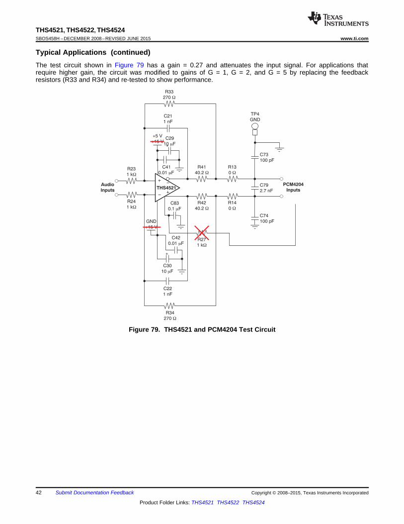
THS4521C79
2.7 nF
C74
100 pF
C73
100 pF
R42
40.2 W
R34
270 W
R24
1 kW
R23
1 kW
R27
1 kW
R41
40.2 W
R33
270 W
C29
10 Fm
C41
0.01 Fm
C42
0.01 Fm
C30
10 Fm
C83
0.1 Fm
R13
0 W
R14
0 W
Audio
Inputs
PCM4204
Inputs
+
C21
1 nF
+
C22
1 nF
TP4
GND
GND
+15 V
+5 V
+15 V
THS4521, THS4522, THS4524SBOS458H –DECEMBER 2008–REVISED JUNE 2015 www.ti.com
Typical Applications (continued)The test circuit shown in Figure 79 has a gain = 0.27 and attenuates the input signal. For applications thatrequire higher gain, the circuit was modified to gains of G = 1, G = 2, and G = 5 by replacing the feedbackresistors (R33 and R34) and re-tested to show performance.
Figure 79. THS4521 and PCM4204 Test Circuit
42 Submit Documentation Feedback Copyright © 2008–2015, Texas Instruments Incorporated
Product Folder Links: THS4521 THS4522 THS4524

THS4521, THS4522, THS4524www.ti.com SBOS458H –DECEMBER 2008–REVISED JUNE 2015
Typical Applications (continued)Figure 84 shows the THS4521 and PCM4204 THD+N versus frequency with no weighting at higher gains.
9.2.1.1 Design Requirements
Table 8. 1-kHz AC Analysis: Test Circuit Versus PCM4204 Data Sheet Typical Specifications(FS = 48 kSPS)
Configuration Tone THD+N Dynamic RangeTHS4521 and PCM4204 1 kHz –106 dBc 117 dB
PCM4204 Data sheet (typ) 1 kHz –105 dBc 118 dB
9.2.1.2 Detailed Design Procedure
Table 9. THS4521EVM Parts ListREFERENCE MANUFACTURER
ITEM DESCRIPTION SMD SIZE DESIGNATOR QTY PART NUMBER1 Capacitor, 10.0 μF, ceramic, X5R, 6.3 V 0805 C7, C8, C9, C10 4 (AVX) 08056D106KAT2A2 Capacitor, 0.1 μF, ceramic, X7R, 16 V 0603 C3, C5, C11, C12 4 (AVX) 0603YC104KAT2A3 Capacitor, 0.22 μF, ceramic, X7R, 10 V 0603 C1, C4, C6 3 (AVX) 0603ZC224KAT2A4 Open 0603 C2, C13, C14, C15, C16 55 Open 0603 R1, R2, R3, R7, R8, R9, R18, 12
R19, R21, R22, R23, R266 Resistor, 0 Ω 0603 R24, R25 2 (ROHM) MCR03EZPJ0007 Resistor, 49.9 Ω, 1/10W, 1% 0603 R6 1 (ROHM) MCR03EZPFX49R98 Resistor, 52.3 Ω, 1/10W, 1% 0603 R10, R11, R20 3 (ROHM) MCR03EZPFX52R39 Resistor, 487 Ω, 1/10W, 1% 0603 R16, R17 2 (ROHM) MCR03EZPFX487010 Resistor, 1k Ω, 1/10W, 1% 0603 R12, R13, R14, R15 4 (ROHM) MCR03EZPFX100111 Resistor, 0 Ω 0805 R4, R5 2 (ROHM) MCR10EZPJ00012 Open T1 113 Transformer, RF T2 1 (MINI-CIRCUITS) ADT1-1WT14 Jack, Banana receptance, 0.25-in dia. J4, J5, J8 3 (SPC) 813
hole15 Open J1, J3, J6, J7, J10, J11 616 Connector, edge, SMA PCB jack J2, J9 2 (JOHNSON) 142-0701-80117 Header, 0.1 in CTRS, 0.025-in sq. pins 2 POS. JP1 1 (SULLINS) PBC36SAAN18 Shunts JP1 1 (SULLINS) SSC02SYAN19 Test point, Red TP1 1 (KEYSTONE) 500020 Test point, Black TP2, TP3 2 (KEYSTONE) 500121 IC, THS4521 U1 1 (TI) THS4521D22 Standoff, 4-40 hex, 0.625 in length 4 (KEYSTONE) 180823 Screw, Phillips, 4-40, .250 in 4 SHR-0440-016-SN24 Board, printed circuit 1 (TI) EDGE# 6494532
Copyright © 2008–2015, Texas Instruments Incorporated Submit Documentation Feedback 43
Product Folder Links: THS4521 THS4522 THS4524
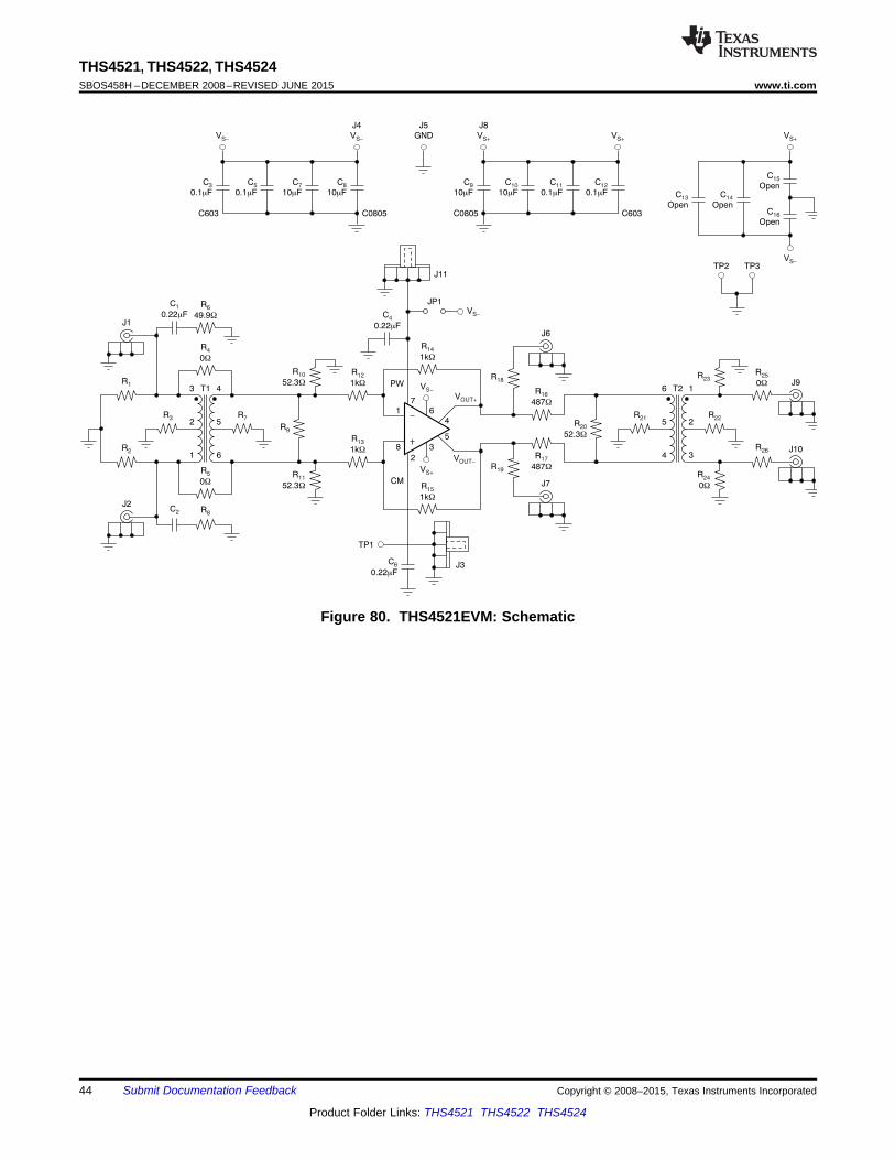
TP2 TP3
C3
0.1 Fm
C603 C0805
C5
0.1 Fm
C8
10 Fm
C7
10 Fm
VS-
J4
VS-
C12
0.1 Fm
C603C0805
C11
0.1 Fm
C9
10 Fm
C10
10 Fm
VS+ VS+
J8
VS+
C15
Open
C16
Open
C13
Open
C14
Open
VS-
J5
GND
R1
R2
R12
1kW
R13
1kW
R14
1kW
R15
1kW
R25
0W J9
J10R26
R16
487W
R20
52.3W
R17
487W
R222
1
3
5
6
4
R21R75
4
6
2
3
1
R3
R4
0W
R6
49.9W
C1
0.22 Fm
R8C2
C4
0.22 Fm
VS-
VS-
VS+
R23R18
R24
0W
R9
R5
0W
R10
52.3W
R11
52.3W
J6
R19
J7
J1
J2
T2T1
TP1
VOUT+
VOUT-
4
5
6
3
1
8
7
2
PW
CM
J11
JP1
J3C6
0.22 Fm
THS4521, THS4522, THS4524SBOS458H –DECEMBER 2008–REVISED JUNE 2015 www.ti.com
Figure 80. THS4521EVM: Schematic
44 Submit Documentation Feedback Copyright © 2008–2015, Texas Instruments Incorporated
Product Folder Links: THS4521 THS4522 THS4524

10
Frequency (Hz)
-80
82
84
86
88
-
-
-
-
-
-
-
-
-
-
90
92
94
96
98
100
TH
D+
N (
dB
)
100 1 k 10 k 20 k
THS4521 and PCM3168 THD+N vs FREQUENCY
(No Weighting)
THS4521, THS4522, THS4524www.ti.com SBOS458H –DECEMBER 2008–REVISED JUNE 2015
9.2.1.2.1 Audio ADC Driver Performance: THS4521 and PCM3168 Combined Performance
The THS4521 is also tested as the drive amplifier for the PCM3168A ADC input. The PCM3168A is a high-performance, single-chip, 24-bit, 6-in/8-out, audio coder/decoder (codec) with single-ended and differentialselectable analog inputs and differential outputs. The six-channel, 24-bit ADC employs a ΔΣ modulator andsupports 8-kHz to 96-kHz sampling rates and a 16-bit/24-bit width digital audio output word on the audiointerface. The eight-channel, 24-bit digital-to-analog converter (DAC) employs a ΔΣ modulator and supports 8-kHz to 192-kHz sampling rates and a 16-bit/24-bit width digital audio input word on the audio interface. Eachaudio interface supports I2S™, left-/right-justified, and DSP formats with 16-bit/24-bit word width. In addition, thePCM3168A supports the time-division-multiplexed (TDM) format.. The PCM3168A provides flexible serial portinterface and many other advanced features. Refer to the PCM3168A product data sheet for more information.
The PCM3168A EVM is used to test the audio performance of the THS4521 as a drive amplifier. The standardPCM3168A EVM is provided with OPA2134 operational amplifiers that are used to convert single-ended inputs todifferential to drive the ADC. For testing, the operational amplifier output series resistors are removed from one ofthe channels and a THS4521, mounted on its standard EVM, is connected to the ADC inputs via short coaxialcables. The THS4521 EVM is configured for both differential inputs as shown in Figure 91 and for single-endedinput as shown in Figure 92 with 1-kΩ resistors for RF and RG, and 24.9-Ω resistors in series with each output toisolate the outputs from the reactive load of the coaxial cables. To limit the noise from the external EVM andcables, a 2.7-nF capacitor is placed differentially across the PCM3168A inputs. The THS4521 is operated with asingle-supply +5-V supply so the output common-mode of the THS4521 defaults to +2.5 V as required at theinput of the PCM3168A. The PCM3168A EVM is configured and operated as described in the PCM3168AEVMUser's Guide. The ADC was tested with an external THS4521 EVM with both single-ended input and differentialinputs. In both configurations, the results are the same. Figure 81 shows the THD+N versus frequency andTable 10 compares the result to the PCM3168 data sheet typical specification at 1 kHz. Both graphs show that itmakes an excellent drive amplifier for this ADC. Note: a 2700 series Audio Analyzer from Audio Precision isused to generate the input signals to the THS4521 and to analyze the digital data from the PCM3168.
Figure 81. THS4521 and PCM3168: Thd+N Versus Frequency With No Weighting
Table 10. 1-kHz AC Analysis: Test Circuit vs PCM3168 Data Sheet Typical Specifications (FS = 48 kSPS)Configuration Tone THD+N
THS4521 and PCM3168 1 kHz –92.6 dBcPCM3168A Data sheet (typ) 1 kHz –93 dBc
Copyright © 2008–2015, Texas Instruments Incorporated Submit Documentation Feedback 45
Product Folder Links: THS4521 THS4522 THS4524

0
Frequency (Hz)
-95
97
99
101
103
-
-
-
-
-
-
-
-
-
-
105
107
109
111
113
115
TH
D+
N (
dB
)
100 1 k 10 k 20 k
G = 5
G = 1
G = 2
THS4521 and PCM4204 THD+N
vs FREQUENCY (No Weighting, at Higher Gains)
0
Frequency (Hz)
-95
97
99
101
103
-
-
-
-
-
-
-
-
-
-
105
107
109
111
113
115
TH
D+
N (
dB
)
100 1 k 10 k 20 k
THS4521 and PCM4204 THD+N
vs FREQUENCY (No Weighting)
0
Frequency (Hz)
0
10
20
30
40
50
-
-
-
-
-
-
-
-
-
-
-
-
-
-
-
60
70
80
90
100
110
120
130
140
150
FF
T (
dB
FS
)
100 1 k 10 k 20 k
THS4521 and PCM4204
1-kHz FFT
THS4521, THS4522, THS4524SBOS458H –DECEMBER 2008–REVISED JUNE 2015 www.ti.com
9.2.1.3 Application Curves
Figure 83. THS4521 and PCM4204 1-kHz FFTFigure 82. THS4521 and PCM4204: Thd+N VersusFrequency With No Weighting
Figure 84. THS4521 and PCM4204: Thd+N Versus Frequency With No Weighting at Higher Gains
46 Submit Documentation Feedback Copyright © 2008–2015, Texas Instruments Incorporated
Product Folder Links: THS4521 THS4522 THS4524
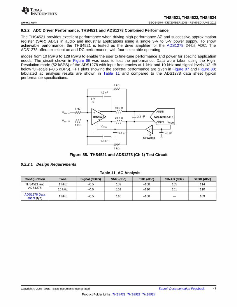
THS4521 ADS1278 (CH 1)
VOCM
5 V
VCOM
2.2 nF
AINN1
AINP1
x1
1/2
OPA2350
1.5 nF
1.5 nF
VIN+
VIN-
1 kW
1 kW
1 kW
49.9 W
49.9 W
0.1 Fm 0.1 Fm
1 kW
THS4521, THS4522, THS4524www.ti.com SBOS458H –DECEMBER 2008–REVISED JUNE 2015
9.2.2 ADC Driver Performance: THS4521 and ADS1278 Combined PerformanceThe THS4521 provides excellent performance when driving high-performance ΔΣ and successive approximationregister (SAR) ADCs in audio and industrial applications using a single 3-V to 5-V power supply. To showachievable performance, the THS4521 is tested as the drive amplifier for the ADS1278 24-bit ADC. TheADS1278 offers excellent ac and DC performance, with four selectable operating
modes from 10 kSPS to 128 kSPS to enable the user to fine-tune performance and power for specific applicationneeds. The circuit shown in Figure 85 was used to test the performance. Data were taken using the High-Resolution mode (52 kSPS) of the ADS1278 with input frequencies at 1 kHz and 10 kHz and signal levels 1/2 dBbelow full-scale (–0.5 dBFS). FFT plots showing the spectral performance are given in Figure 87 and Figure 88;tabulated ac analysis results are shown in Table 11 and compared to the ADS1278 data sheet typicalperformance specifications.
Figure 85. THS4521 and ADS1278 (Ch 1) Test Circuit
9.2.2.1 Design Requirements
Table 11. AC AnalysisConfiguration Tone Signal (dBFS) SNR (dBc) THD (dBc) SINAD (dBc) SFDR (dBc)THS4521 and 1 kHz –0.5 109 –108 105 114
ADS1278 10 kHz –0.5 102 –110 101 110ADS1278 Data 1 kHz –0.5 110 –108 — 109sheet (typ)
Copyright © 2008–2015, Texas Instruments Incorporated Submit Documentation Feedback 47
Product Folder Links: THS4521 THS4522 THS4524
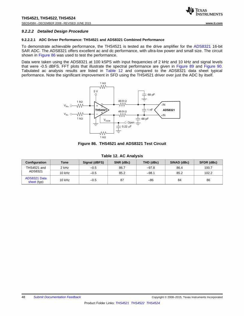
THS4521 ADS8321
VOCM
5 V
1 nF
-IN
+IN
VIN+
VIN-
1 kW
1 kW
1 kW
49.9 W
49.9 W
0.22 Fm
68 pF
68 pF
1 kW
Open
THS4521, THS4522, THS4524SBOS458H –DECEMBER 2008–REVISED JUNE 2015 www.ti.com
9.2.2.2 Detailed Design Procedure
9.2.2.2.1 ADC Driver Performance: THS4521 and ADS8321 Combined Performance
To demonstrate achievable performance, the THS4521 is tested as the drive amplifier for the ADS8321 16-bitSAR ADC. The ADS8321 offers excellent ac and dc performance, with ultra-low power and small size. The circuitshown in Figure 86 was used to test the performance.
Data were taken using the ADS8321 at 100 kSPS with input frequencies of 2 kHz and 10 kHz and signal levelsthat were -0.5 dBFS. FFT plots that illustrate the spectral performance are given in Figure 89 and Figure 90.Tabulated ac analysis results are listed in Table 12 and compared to the ADS8321 data sheet typicalperformance. Note the significant improvement in SFD using the THS4521 driver over just the ADC by itself.
Figure 86. THS4521 and ADS8321 Test Circuit
Table 12. AC AnalysisConfiguration Tone Signal (dBFS) SNR (dBc) THD (dBc) SINAD (dBc) SFDR (dBc)THS4521 and 2 kHz –0.5 86.7 –97.8 86.4 100.7
ADS8321 10 kHz –0.5 85.2 –98.1 85.2 102.2ADS8321 Data 10 kHz –0.5 87 –86 84 86sheet (typ)
48 Submit Documentation Feedback Copyright © 2008–2015, Texas Instruments Incorporated
Product Folder Links: THS4521 THS4522 THS4524

0
20
40
60
80
100
120
140
-
-
-
-
-
-
-
-160
Ma
gn
itu
de
(d
BF
S)
0 10 k 20 k 30 k 40 k 50 k
Frequency (Hz)
V = 5.0 V
G = 1 V/V
R = 1 k
S
F R =
Load = 2 x 49.9 + 2 pFG W
W
10-kHz FFT
0
20
40
60
80
100
120
140
160
-
-
-
-
-
-
-
-
Ma
gn
itud
e (
dB
FS
)
0 4 8 12 16 20 24 26
Frequency (kHz)
10-kHz FFT
G = 1
R = R = 1 k
C = 1.5 nF
V = 5 V
Load = 2 x 49.9 + 2.2 nF
F G
F
S
W
W
0
20
40
60
80
100
120
140
160
-
-
-
-
-
-
-
-
Ma
gnitud
e (
dB
FS
)
0 4 8 12 16 20 24 26
Frequency (kHz)
1-kHz FFT
G = 1
R = R = 1 k
C = 1.5 nF
V = 5 V
Load = 2 x 49.9 + 2.2 nF
F G
F
S
W
W
0
20
40
60
80
100
120
140
160
-
-
-
-
-
-
-
-
Ma
gnitud
e (
dB
FS
)
0 4 8 12 16 20 24 26
Frequency (kHz)
10-kHz FFT
G = 1
R = R = 1 k
C = 1.5 nF
V = 5 V
Load = 2 x 49.9 + 2.2 nF
F G
F
S
W
W
THS4521, THS4522, THS4524www.ti.com SBOS458H –DECEMBER 2008–REVISED JUNE 2015
9.2.2.3 Application CurvesThe application curves below apply to the ADS14278 test.
Figure 88. 10-kHz FFTFigure 87. 1-kHz FFT
The application curves below apply to the ADS8321 test.
Figure 89. 2-kHZ FFT Figure 90. 10-kHz FFT
Copyright © 2008–2015, Texas Instruments Incorporated Submit Documentation Feedback 49
Product Folder Links: THS4521 THS4522 THS4524
THS452x
VOUT-
VOUT+
RF
RF
RG
RGSingle-Ended
Input
Differential
Output
VS+
VS-
THS452x
VOUT-
VIN- VOUT+
VIN+
RF
RF
RG
RG
Differential
Input
Differential
Output
VS+
VS-
THS4521, THS4522, THS4524SBOS458H –DECEMBER 2008–REVISED JUNE 2015 www.ti.com
9.2.3 Differential Input to Differential Output AmplifierThe THS4521, THS4522, and THS4524 family are fully-differential operational amplifiers that can be used toamplify differential input signals to differential output signals. Figure 91 shows a basic block diagram of the circuit(VOCM and PD inputs not shown). The gain of the circuit is set by RF divided by RG.
Figure 91. Differential Input to Differential Output Amplifier
9.2.4 Single-Ended Input to Differential Output AmplifierThe THS4521, THS4522, and THS4524 family can also amplify and convert single-ended input signals todifferential output signals. Figure 92 illustrates a basic block diagram of the circuit (VOCM and PD inputs notshown). The gain of the circuit is again set by RF divided by RG.
Figure 92. Single-Ended Input to Differential Output Amplifier
50 Submit Documentation Feedback Copyright © 2008–2015, Texas Instruments Incorporated
Product Folder Links: THS4521 THS4522 THS4524

THS4521, THS4522, THS4524www.ti.com SBOS458H –DECEMBER 2008–REVISED JUNE 2015
10 Power Supply RecommendationsThe THS452x family is principally intended to operate with a nominal single-supply voltage of +3 V to +5 V.Supply-voltage tolerances are supported with the specified operating range of 2.5 V (10% low on a 3-V nominalsupply) and 5.5 V (8% high on a 5-V nominal supply). Supply decoupling is required, as described in theApplication and Implementation. Split (or bipolar) supplies can be used with the THS452x family, as long as thetotal value across the device remains less than 5.5 V (absolute maximum).
Using a negative supply to deliver a true swing to ground output in driving SAR ADCs may be desired. While theTHS452x family quotes a rail-to-rail output, linear operation requires approximately a 200-mV headroom to thesupply rails. One easy option for extending the linear output swing to ground is to provide the small negativesupply voltage required using the LM7705 fixed –230-mV, negative-supply generator. This low-cost, fixednegative-supply generator accepts the 3- to 5-V positive supply input used by the THS452x and provides a –230-mV supply for the negative rail. Using the LM7705 provides an effective solution, as shown in the TI DesignsTIDU187, Extending Rail-to-Rail Output Range for Fully Differential Amplifiers to Include True Zero Volts.
11 Layout
11.1 Layout GuidelinesFigure 80 shows the THS4521EVM schematic. PCB layers 1 through 4 are shown in Figure 93; Table 9 lists thebill of materials for the THS4521EVM as supplied from TI. It is recommended to follow the layout of the externalcomponents near to the amplifier, ground plane construction, and power routing as closely as possible. Followthese general guidelines:• Signal routing should be direct and as short as possible into and out of the amplifier circuit.• The feedback path should be short and direct.• Ground or power planes should be removed from directly under the amplifier input and output pins.• An output resistor is recommended in each output lead, placed as near to the output pins as possible.• Two 0.1-μF power-supply decoupling capacitors should be placed as near to the power-supply pins as
possible.• Two 10-μF power-supply decoupling capacitors should be placed within 1 inch of the device and can be
shared among multiple analog devices.• A 0.22-μF capacitor should be placed between the VOCM input pin and ground near to the pin. This capacitor
limits noise coupled into the pin.• The PD pin uses TTL logic levels; a bypass capacitor is not necessary if actively driven, but can be used for
robustness in noisy environments whether driven or not.• If input termination resistors R10 and R11 are used, a single point connection to ground on L2 is
recommended.
Copyright © 2008–2015, Texas Instruments Incorporated Submit Documentation Feedback 51
Product Folder Links: THS4521 THS4522 THS4524

THS4521, THS4522, THS4524SBOS458H –DECEMBER 2008–REVISED JUNE 2015 www.ti.com
11.2 Layout Example
Figure 93. THS4521EVM: Layer 1 to Layer 4 Images
52 Submit Documentation Feedback Copyright © 2008–2015, Texas Instruments Incorporated
Product Folder Links: THS4521 THS4522 THS4524
THS4521, THS4522, THS4524www.ti.com SBOS458H –DECEMBER 2008–REVISED JUNE 2015
12 Device and Documentation Support
12.1 Device Support
12.1.1 Third-Party Products DisclaimerTI'S PUBLICATION OF INFORMATION REGARDING THIRD-PARTY PRODUCTS OR SERVICES DOES NOTCONSTITUTE AN ENDORSEMENT REGARDING THE SUITABILITY OF SUCH PRODUCTS OR SERVICESOR A WARRANTY, REPRESENTATION OR ENDORSEMENT OF SUCH PRODUCTS OR SERVICES, EITHERALONE OR IN COMBINATION WITH ANY TI PRODUCT OR SERVICE.
12.2 Related LinksTable 13 lists quick access links. Categories include technical documents, support and community resources,tools and software, and quick access to sample or buy.
Table 13. Related LinksTECHNICAL TOOLS & SUPPORT &PARTS PRODUCT FOLDER SAMPLE & BUY DOCUMENTS SOFTWARE COMMUNITY
THS4521 Click here Click here Click here Click here Click hereTHS4522 Click here Click here Click here Click here Click hereTHS4524 Click here Click here Click here Click here Click here
12.3 Community ResourcesThe following links connect to TI community resources. Linked contents are provided "AS IS" by the respectivecontributors. They do not constitute TI specifications and do not necessarily reflect TI's views; see TI's Terms ofUse.
TI E2E™ Online Community TI's Engineer-to-Engineer (E2E) Community. Created to foster collaborationamong engineers. At e2e.ti.com, you can ask questions, share knowledge, explore ideas and helpsolve problems with fellow engineers.
Design Support TI's Design Support Quickly find helpful E2E forums along with design support tools andcontact information for technical support.
12.4 TrademarksE2E is a trademark of Texas Instruments.I2S is a trademark of NXP Semiconductor.All other trademarks are the property of their respective owners.
12.5 Electrostatic Discharge CautionThis integrated circuit can be damaged by ESD. Texas Instruments recommends that all integrated circuits be handled withappropriate precautions. Failure to observe proper handling and installation procedures can cause damage.
ESD damage can range from subtle performance degradation to complete device failure. Precision integrated circuits may be moresusceptible to damage because very small parametric changes could cause the device not to meet its published specifications.
12.6 GlossarySLYZ022 — TI Glossary.
This glossary lists and explains terms, acronyms, and definitions.
13 Mechanical, Packaging, and Orderable InformationThe following pages include mechanical, packaging, and orderable information. This information is the mostcurrent data available for the designated devices. This data is subject to change without notice and revision ofthis document. For browser-based versions of this data sheet, refer to the left-hand navigation.
Copyright © 2008–2015, Texas Instruments Incorporated Submit Documentation Feedback 53
Product Folder Links: THS4521 THS4522 THS4524
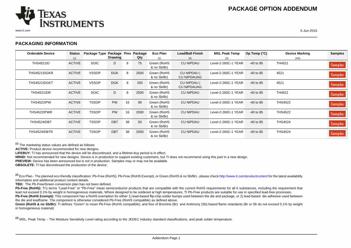
PACKAGE OPTION ADDENDUM
www.ti.com 5-Jun-2015
Addendum-Page 1
PACKAGING INFORMATION
Orderable Device Status(1)
Package Type PackageDrawing
Pins PackageQty
Eco Plan(2)
Lead/Ball Finish(6)
MSL Peak Temp(3)
Op Temp (°C) Device Marking(4/5)
Samples
THS4521ID ACTIVE SOIC D 8 75 Green (RoHS& no Sb/Br)
CU NIPDAU Level-2-260C-1 YEAR -40 to 85 TH4521
THS4521IDGKR ACTIVE VSSOP DGK 8 2500 Green (RoHS& no Sb/Br)
CU NIPDAU |CU NIPDAUAG
Level-2-260C-1 YEAR -40 to 85 4521
THS4521IDGKT ACTIVE VSSOP DGK 8 250 Green (RoHS& no Sb/Br)
CU NIPDAU |CU NIPDAUAG
Level-2-260C-1 YEAR -40 to 85 4521
THS4521IDR ACTIVE SOIC D 8 2500 Green (RoHS& no Sb/Br)
CU NIPDAU Level-2-260C-1 YEAR -40 to 85 TH4521
THS4522IPW ACTIVE TSSOP PW 16 90 Green (RoHS& no Sb/Br)
CU NIPDAU Level-2-260C-1 YEAR -40 to 85 THS4522
THS4522IPWR ACTIVE TSSOP PW 16 2000 Green (RoHS& no Sb/Br)
CU NIPDAU Level-2-260C-1 YEAR -40 to 85 THS4522
THS4524IDBT ACTIVE TSSOP DBT 38 50 Green (RoHS& no Sb/Br)
CU NIPDAU Level-2-260C-1 YEAR -40 to 85 THS4524
THS4524IDBTR ACTIVE TSSOP DBT 38 2000 Green (RoHS& no Sb/Br)
CU NIPDAU Level-2-260C-1 YEAR -40 to 85 THS4524
(1) The marketing status values are defined as follows:ACTIVE: Product device recommended for new designs.LIFEBUY: TI has announced that the device will be discontinued, and a lifetime-buy period is in effect.NRND: Not recommended for new designs. Device is in production to support existing customers, but TI does not recommend using this part in a new design.PREVIEW: Device has been announced but is not in production. Samples may or may not be available.OBSOLETE: TI has discontinued the production of the device.
(2) Eco Plan - The planned eco-friendly classification: Pb-Free (RoHS), Pb-Free (RoHS Exempt), or Green (RoHS & no Sb/Br) - please check http://www.ti.com/productcontent for the latest availabilityinformation and additional product content details.TBD: The Pb-Free/Green conversion plan has not been defined.Pb-Free (RoHS): TI's terms "Lead-Free" or "Pb-Free" mean semiconductor products that are compatible with the current RoHS requirements for all 6 substances, including the requirement thatlead not exceed 0.1% by weight in homogeneous materials. Where designed to be soldered at high temperatures, TI Pb-Free products are suitable for use in specified lead-free processes.Pb-Free (RoHS Exempt): This component has a RoHS exemption for either 1) lead-based flip-chip solder bumps used between the die and package, or 2) lead-based die adhesive used betweenthe die and leadframe. The component is otherwise considered Pb-Free (RoHS compatible) as defined above.Green (RoHS & no Sb/Br): TI defines "Green" to mean Pb-Free (RoHS compatible), and free of Bromine (Br) and Antimony (Sb) based flame retardants (Br or Sb do not exceed 0.1% by weightin homogeneous material)
(3) MSL, Peak Temp. - The Moisture Sensitivity Level rating according to the JEDEC industry standard classifications, and peak solder temperature.

PACKAGE OPTION ADDENDUM
www.ti.com 5-Jun-2015
Addendum-Page 2
(4) There may be additional marking, which relates to the logo, the lot trace code information, or the environmental category on the device.
(5) Multiple Device Markings will be inside parentheses. Only one Device Marking contained in parentheses and separated by a "~" will appear on a device. If a line is indented then it is a continuationof the previous line and the two combined represent the entire Device Marking for that device.
(6) Lead/Ball Finish - Orderable Devices may have multiple material finish options. Finish options are separated by a vertical ruled line. Lead/Ball Finish values may wrap to two lines if the finishvalue exceeds the maximum column width.
Important Information and Disclaimer:The information provided on this page represents TI's knowledge and belief as of the date that it is provided. TI bases its knowledge and belief on informationprovided by third parties, and makes no representation or warranty as to the accuracy of such information. Efforts are underway to better integrate information from third parties. TI has taken andcontinues to take reasonable steps to provide representative and accurate information but may not have conducted destructive testing or chemical analysis on incoming materials and chemicals.TI and TI suppliers consider certain information to be proprietary, and thus CAS numbers and other limited information may not be available for release.
In no event shall TI's liability arising out of such information exceed the total purchase price of the TI part(s) at issue in this document sold by TI to Customer on an annual basis.
OTHER QUALIFIED VERSIONS OF THS4521, THS4524 :
• Enhanced Product: THS4524-EP
NOTE: Qualified Version Definitions:
• Enhanced Product - Supports Defense, Aerospace and Medical Applications

TAPE AND REEL INFORMATION
*All dimensions are nominal
Device PackageType
PackageDrawing
Pins SPQ ReelDiameter
(mm)
ReelWidth
W1 (mm)
A0(mm)
B0(mm)
K0(mm)
P1(mm)
W(mm)
Pin1Quadrant
THS4521IDGKR VSSOP DGK 8 2500 330.0 12.4 5.3 3.4 1.4 8.0 12.0 Q1
THS4521IDGKT VSSOP DGK 8 250 180.0 12.4 5.3 3.4 1.4 8.0 12.0 Q1
THS4521IDR SOIC D 8 2500 330.0 12.4 6.4 5.2 2.1 8.0 12.0 Q1
THS4522IPWR TSSOP PW 16 2000 330.0 12.4 6.9 5.6 1.6 8.0 12.0 Q1
THS4524IDBTR TSSOP DBT 38 2000 330.0 16.4 6.9 10.2 1.8 12.0 16.0 Q1
PACKAGE MATERIALS INFORMATION
www.ti.com 16-Jan-2018
Pack Materials-Page 1

*All dimensions are nominal
Device Package Type Package Drawing Pins SPQ Length (mm) Width (mm) Height (mm)
THS4521IDGKR VSSOP DGK 8 2500 367.0 367.0 35.0
THS4521IDGKT VSSOP DGK 8 250 210.0 185.0 35.0
THS4521IDR SOIC D 8 2500 367.0 367.0 35.0
THS4522IPWR TSSOP PW 16 2000 367.0 367.0 35.0
THS4524IDBTR TSSOP DBT 38 2000 367.0 367.0 38.0
PACKAGE MATERIALS INFORMATION
www.ti.com 16-Jan-2018
Pack Materials-Page 2
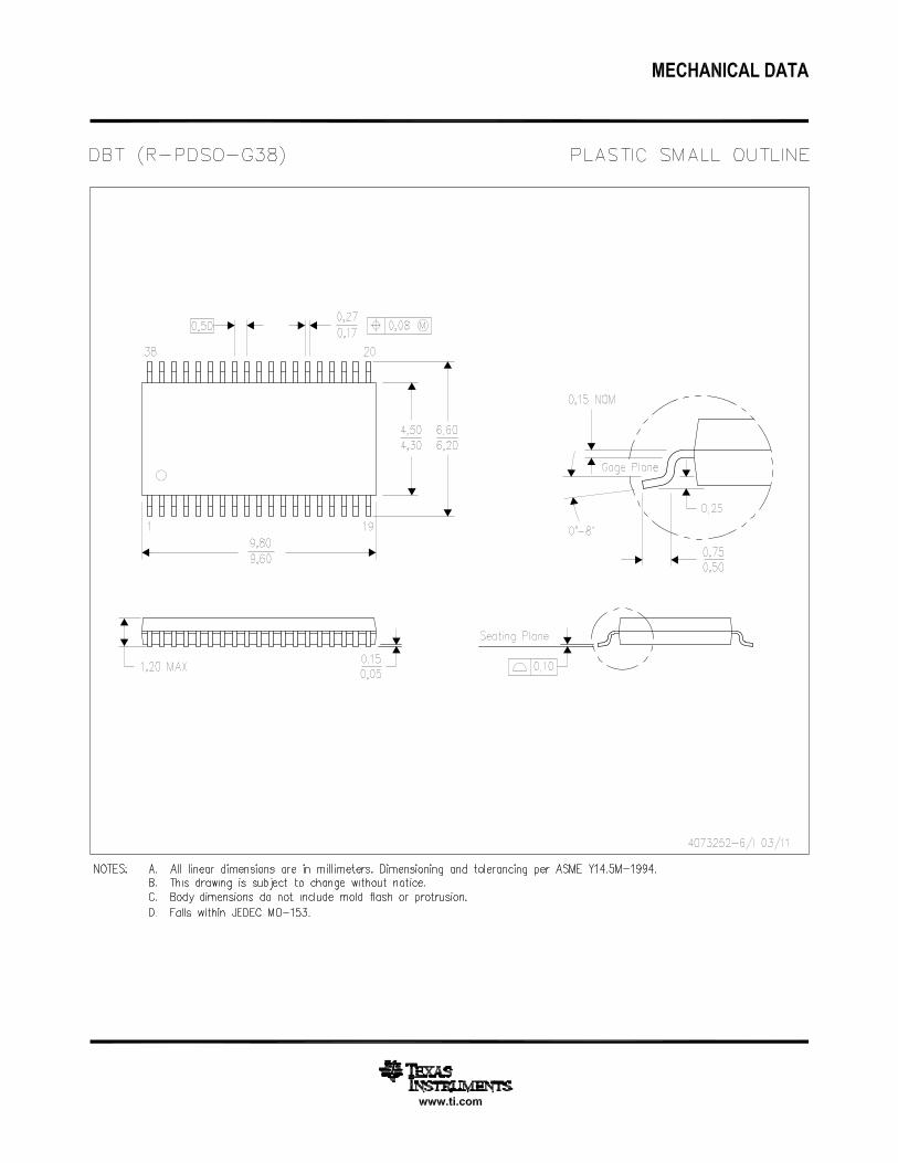


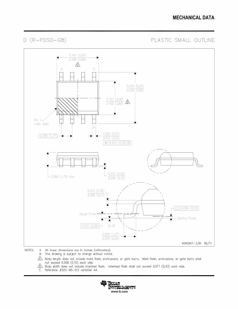

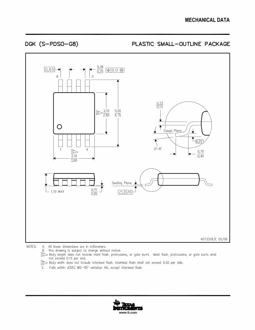


IMPORTANT NOTICE
Texas Instruments Incorporated (TI) reserves the right to make corrections, enhancements, improvements and other changes to itssemiconductor products and services per JESD46, latest issue, and to discontinue any product or service per JESD48, latest issue. Buyersshould obtain the latest relevant information before placing orders and should verify that such information is current and complete.TI’s published terms of sale for semiconductor products (http://www.ti.com/sc/docs/stdterms.htm) apply to the sale of packaged integratedcircuit products that TI has qualified and released to market. Additional terms may apply to the use or sale of other types of TI products andservices.Reproduction of significant portions of TI information in TI data sheets is permissible only if reproduction is without alteration and isaccompanied by all associated warranties, conditions, limitations, and notices. TI is not responsible or liable for such reproduceddocumentation. Information of third parties may be subject to additional restrictions. Resale of TI products or services with statementsdifferent from or beyond the parameters stated by TI for that product or service voids all express and any implied warranties for theassociated TI product or service and is an unfair and deceptive business practice. TI is not responsible or liable for any such statements.Buyers and others who are developing systems that incorporate TI products (collectively, “Designers”) understand and agree that Designersremain responsible for using their independent analysis, evaluation and judgment in designing their applications and that Designers havefull and exclusive responsibility to assure the safety of Designers' applications and compliance of their applications (and of all TI productsused in or for Designers’ applications) with all applicable regulations, laws and other applicable requirements. Designer represents that, withrespect to their applications, Designer has all the necessary expertise to create and implement safeguards that (1) anticipate dangerousconsequences of failures, (2) monitor failures and their consequences, and (3) lessen the likelihood of failures that might cause harm andtake appropriate actions. Designer agrees that prior to using or distributing any applications that include TI products, Designer willthoroughly test such applications and the functionality of such TI products as used in such applications.TI’s provision of technical, application or other design advice, quality characterization, reliability data or other services or information,including, but not limited to, reference designs and materials relating to evaluation modules, (collectively, “TI Resources”) are intended toassist designers who are developing applications that incorporate TI products; by downloading, accessing or using TI Resources in anyway, Designer (individually or, if Designer is acting on behalf of a company, Designer’s company) agrees to use any particular TI Resourcesolely for this purpose and subject to the terms of this Notice.TI’s provision of TI Resources does not expand or otherwise alter TI’s applicable published warranties or warranty disclaimers for TIproducts, and no additional obligations or liabilities arise from TI providing such TI Resources. TI reserves the right to make corrections,enhancements, improvements and other changes to its TI Resources. TI has not conducted any testing other than that specificallydescribed in the published documentation for a particular TI Resource.Designer is authorized to use, copy and modify any individual TI Resource only in connection with the development of applications thatinclude the TI product(s) identified in such TI Resource. NO OTHER LICENSE, EXPRESS OR IMPLIED, BY ESTOPPEL OR OTHERWISETO ANY OTHER TI INTELLECTUAL PROPERTY RIGHT, AND NO LICENSE TO ANY TECHNOLOGY OR INTELLECTUAL PROPERTYRIGHT OF TI OR ANY THIRD PARTY IS GRANTED HEREIN, including but not limited to any patent right, copyright, mask work right, orother intellectual property right relating to any combination, machine, or process in which TI products or services are used. Informationregarding or referencing third-party products or services does not constitute a license to use such products or services, or a warranty orendorsement thereof. Use of TI Resources may require a license from a third party under the patents or other intellectual property of thethird party, or a license from TI under the patents or other intellectual property of TI.TI RESOURCES ARE PROVIDED “AS IS” AND WITH ALL FAULTS. TI DISCLAIMS ALL OTHER WARRANTIES ORREPRESENTATIONS, EXPRESS OR IMPLIED, REGARDING RESOURCES OR USE THEREOF, INCLUDING BUT NOT LIMITED TOACCURACY OR COMPLETENESS, TITLE, ANY EPIDEMIC FAILURE WARRANTY AND ANY IMPLIED WARRANTIES OFMERCHANTABILITY, FITNESS FOR A PARTICULAR PURPOSE, AND NON-INFRINGEMENT OF ANY THIRD PARTY INTELLECTUALPROPERTY RIGHTS. TI SHALL NOT BE LIABLE FOR AND SHALL NOT DEFEND OR INDEMNIFY DESIGNER AGAINST ANY CLAIM,INCLUDING BUT NOT LIMITED TO ANY INFRINGEMENT CLAIM THAT RELATES TO OR IS BASED ON ANY COMBINATION OFPRODUCTS EVEN IF DESCRIBED IN TI RESOURCES OR OTHERWISE. IN NO EVENT SHALL TI BE LIABLE FOR ANY ACTUAL,DIRECT, SPECIAL, COLLATERAL, INDIRECT, PUNITIVE, INCIDENTAL, CONSEQUENTIAL OR EXEMPLARY DAMAGES INCONNECTION WITH OR ARISING OUT OF TI RESOURCES OR USE THEREOF, AND REGARDLESS OF WHETHER TI HAS BEENADVISED OF THE POSSIBILITY OF SUCH DAMAGES.Unless TI has explicitly designated an individual product as meeting the requirements of a particular industry standard (e.g., ISO/TS 16949and ISO 26262), TI is not responsible for any failure to meet such industry standard requirements.Where TI specifically promotes products as facilitating functional safety or as compliant with industry functional safety standards, suchproducts are intended to help enable customers to design and create their own applications that meet applicable functional safety standardsand requirements. Using products in an application does not by itself establish any safety features in the application. Designers mustensure compliance with safety-related requirements and standards applicable to their applications. Designer may not use any TI products inlife-critical medical equipment unless authorized officers of the parties have executed a special contract specifically governing such use.Life-critical medical equipment is medical equipment where failure of such equipment would cause serious bodily injury or death (e.g., lifesupport, pacemakers, defibrillators, heart pumps, neurostimulators, and implantables). Such equipment includes, without limitation, allmedical devices identified by the U.S. Food and Drug Administration as Class III devices and equivalent classifications outside the U.S.TI may expressly designate certain products as completing a particular qualification (e.g., Q100, Military Grade, or Enhanced Product).Designers agree that it has the necessary expertise to select the product with the appropriate qualification designation for their applicationsand that proper product selection is at Designers’ own risk. Designers are solely responsible for compliance with all legal and regulatoryrequirements in connection with such selection.Designer will fully indemnify TI and its representatives against any damages, costs, losses, and/or liabilities arising out of Designer’s non-compliance with the terms and provisions of this Notice.
Mailing Address: Texas Instruments, Post Office Box 655303, Dallas, Texas 75265Copyright © 2018, Texas Instruments Incorporated