Embed Size (px)
Citation preview

1
CAD for VLSI 1
VERILOGHardware Description Language
CAD for VLSI 2
About Verilog
• Along with VHDL, Verilog is among the most widely used HDLs.
• Main differences:
– VHDL was designed to support system-level design and specification.
– Verilog was designed primarily for digital hardware designers developing FPGAs and ASICs.

2
CAD for VLSI 3
Concept of Verilog “Module”
• In Verilog, the basic unit of hardware is called a module.
– Modules cannot contain definitions of other modules.
– A module can, however, be instantiated within another module.
– Allows the creation of a hierarchy in a Verilog description.
CAD for VLSI 4
Basic Syntax of Module Definition
module module_name (list_of_ports);
input/output declarations;
local net declarations;
parallel statements;
endmodule
3
CAD for VLSI 5
Example 1 :: simple AND gate
module simpleand (f, x, y);
input x, y;
output f;
assign f = x & y;
endmodule
CAD for VLSI 6
Example 2 :: two-level circuit
module two_level (a, b, c, d, f);input a, b, c, d;output f;wire t1, t2;assign t1 = a & b;assign t2 = ~ (c | d);assign f = t1 ^ t2;
endmodule

4
CAD for VLSI 7
Variable Data Types
• A variable belongs to one of two data types:– Net
• Must be continuously driven
• Used to model connections between continuous assignments & instantiations
– Register
• Retains the last value assigned to it
• Often used to represent storage elements
CAD for VLSI 8
Net data type– Different ‘net’ types supported for
synthesis:
• wire, wor, wand, tri, supply0, supply1
– ‘wire’ and ‘tri’ are equivalent; when there are multiple drivers driving them, the outputs of the drivers are shorted together.
– ‘wor’ / ‘wand’ inserts an OR / AND gate at the connection.
– ‘supply0’ / ‘supply1’ model power supply connections.
5
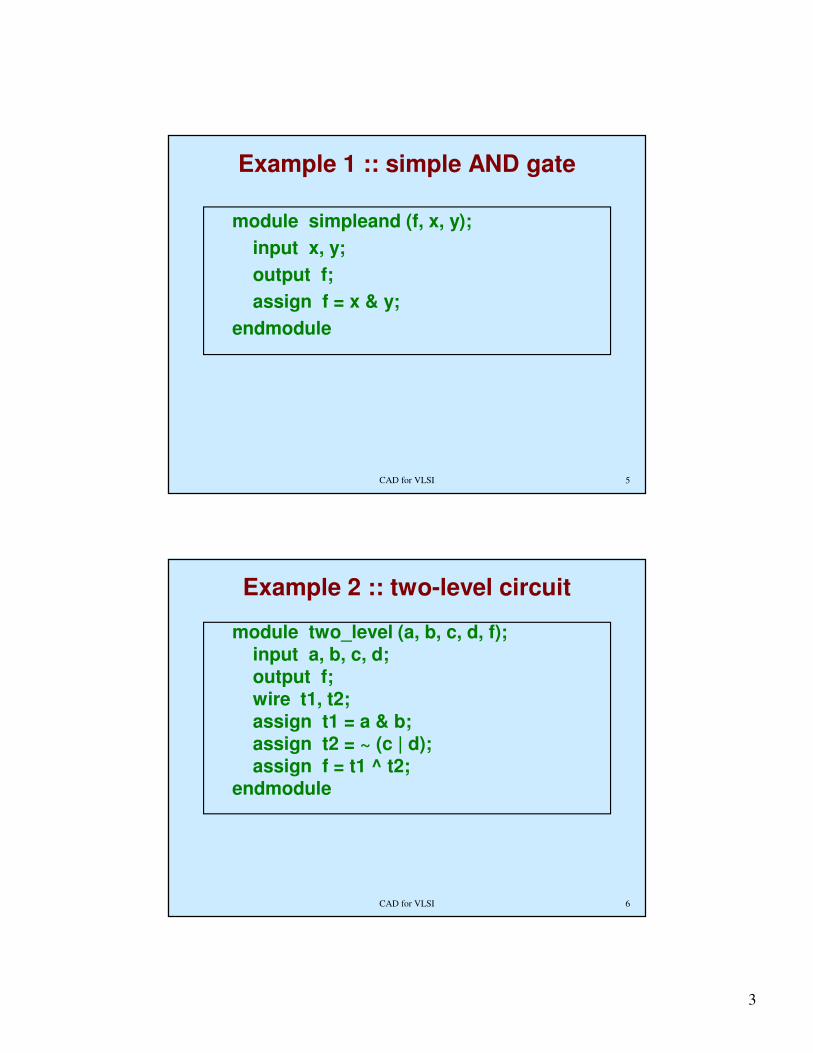
CAD for VLSI 9
module using_wired_and (A, B, C, D, f);input A, B, C, D;output f;wand f; // net f declared as ‘wand’
assign f = A & B;assign f = C | D;
endmodule
CAD for VLSI 10
module using_supply_wire (A, B, C, f);
input A, B, C;
output f;
supply0 gnd;
supply1 vdd;
nand G1 (t1, vdd, A, B);
xor G2 (t2, C, gnd);
and G3 (f, t1, t2);
endmodule

6
CAD for VLSI 11
Register data type
– Different ‘register’ types supported for synthesis:
• reg, integer
– The ‘reg’ declaration explicitly specifies the size.
reg x, y; // single-bit register variables
reg [15:0] bus; // 16-bit bus, bus[15] MSB
– For ‘integer’, it takes the default size, usually 32-bits.
• Synthesizer tries to determine the size.
CAD for VLSI 12
Other differences:– In arithmetic expressions,
• An ‘integer’ is treated as a 2’s complement signed integer.
• A ‘reg’ is treated as an unsigned quantity.
– General rule of thumb
• ‘reg’ used to model actual hardware registers such as counters, accumulator, etc.
• ‘integer’ used for situations like loop counting.

7
CAD for VLSI 13
module simple_counter (clk, rst, count);input clk, rst;output count;reg [31:0] count;
always @(posedge clk)begin
if (rst)count = 32’b0;
elsecount = count + 1;
endendmodule
CAD for VLSI 14
• When ‘integer’ is used, the synthesis system often carries out a data flow analysis of the model to determine its actual size.
• Example:
wire [1:10] A, B;
integer C;
C = A + B;
�The size of C can be determined to be
equal to 11 (ten bits plus a carry).

8
CAD for VLSI 15
Specifying Constant Values
• A value may be specified in either the ‘sized’ or the ‘un-sized’ form.
– Syntax for ‘sized’ form:
<size>’<base><number>
• Examples:8’b01110011 // 8-bit binary number
12’hA2D // 1010 0010 1101 in binary
12’hCx5 // 1100 xxxx 0101 in binary
25 // signed number, 32 bits
1’b0 // logic 0
1’b1 // logic 1
CAD for VLSI 16
Parameters
• A parameter is a constant with a name.
• No size is allowed to be specified for a parameter.
– The size gets decided from the constant itself (32-bits if nothing is specified).
• Examples:
parameter HI = 25, LO = 5;
parameter up = 2b’00, down = 2b’01,
steady = 2b’10;

9
CAD for VLSI 17
Logic Values
• The common values used in modeling hardware are:
0 :: Logic-0 or FALSE
1 :: Logic-1 or TRUE
x :: Unknown (or don’t care)
z :: High impedance
• Initialization:
– All unconnected nets set to ‘z’
– All register variables set to ‘x’
CAD for VLSI 18
• Verilog provides a set of predefined logic gates.
– They respond to inputs (0, 1, x, or z) in a logical way.
– Example :: AND
0 & 0 ���� 0 0 & x ���� 0
0 & 1 ���� 0 1 & z ���� x
1 & 1 ���� 1 z & x ���� x
1 & x ���� x

10
CAD for VLSI 19
Primitive Gates
• Primitive logic gates (instantiations):
and G (out, in1, in2);
nand G (out, in1, in2);
or G (out, in1, in2);
nor G (out, in1, in2);
xor G (out, in1, in2);
xnor G (out, in1, in2);
not G (out1, in);
buf G (out1, in);
CAD for VLSI 20
• Primitive Tri-State gates (instantiation)
bufif1 G (out, in, ctrl);
bufif0 G (out, in, ctrl);
notif1 G (out, in, ctrl);
notif0 G (out, in, ctrl);

11
CAD for VLSI 21
Some Points to Note
• For all primitive gates,
– The output port must be connected to a net (a wire).
– The input ports may be connected to nets or register type variables.
– They can have a single output but any number of inputs.
– An optional delay may be specified.
• Logic synthesis tools ignore time delays.
CAD for VLSI 22
`timescale 1 ns / 1ns
module exclusive_or (f, a, b);
input a, b;
output f;
wire t1, t2, t3;
nand #5 m1 (t1, a, b);
and #5 m2 (t2, a, t1);
and #5 m3 (t3, t1, b);
or #5 m4 (f, t2, t3);
endmodule

12
CAD for VLSI 23
Hardware Modeling Issues
• The values computed can be held in
– A ‘wire’
– A ‘flip-flop’ (edge-triggered storage cell)
– A ‘latch’ (level-sensitive storage cell)
• A variable in Verilog can be of
– ‘net data type
• Maps to a ‘wire’ during synthesis
– ‘register’ data type
• Maps either to a ‘wire’ or to a ‘storage cell’ depending on the context under which a value is assigned.
CAD for VLSI 24
module reg_maps_to_wire (A, B, C, f1, f2);input A, B, C;output f1, f2;wire A, B, C;reg f1, f2;always @(A or B or C)begin
f1 = ~(A & B);f2 = f1 ^ C;
endendmodule
The synthesis systemwill generate a wire for f1

13
CAD for VLSI 25
module a_problem_case (A, B, C, f1, f2);input A, B, C;output f1, f2;wire A, B, C;reg f1, f2;always @(A or B or C)begin
f2 = f1 ^ f2;f1 = ~(A & B);
endendmodule
The synthesis systemwill not generate a storage cell for f1
CAD for VLSI 26
// A latch gets inferred heremodule simple_latch (data, load, d_out);
input data, load;output d_out;
always @(load or data)begin
if (!load)t = data;
d_out = !t;end
endmodule
Else part missing; solatch is inferred.

14
CAD for VLSI 27
Verilog Operators
• Arithmetic operators
*, /, +, -, %
• Logical operators
! ���� logical negation
&& ���� logical AND
| | ���� logical OR
• Relational operators
>, <, >=, <=, ==, !=
• Bitwise operators~, &, |, ^, ~^
CAD for VLSI 28
• Reduction operators (operate on all the bits within a word)
&, ~&, |, ~|, ^, ~^
���� accepts a single word operand and
produces a single bit as output
• Shift operators
>>, <<
• Concatenation { }
• Replication { n { } }
• Conditional
<condition> ? <expression1> : <expression2>

15
CAD for VLSI 29
// An 8-bit adder description
module parallel_adder (sum, cout, in1, in2, cin);
input [7:0] in1, in2; input cin;
output [7:0] sum; output cout;
assign #20 {cout, sum} = in1 + in2 + cin;
endmodule
CAD for VLSI 30
Some Points
• The presence of a ‘z’ or ‘x’ in a reg or wirebeing used in an arithmetic expression results in the whole expression being unknown (‘x’).
• The logical operators (!, &&, | |) all evaluate to a 1-bit result (0, 1 or x).
• The relational operators (>, <, <=, >=, ~=, ==) also evaluate to a 1-bit result (0 or 1).
• Boolean false is equivalent to 1’b0
Boolean true is equivalent to 1’b1.

16
CAD for VLSI 31
Some Valid Statements
assign outp = (p == 4’b1111);
if (load && (select == 2’b01)) …….
assign a = b >> 1;
assign a = b << 3;
assign f = {a, b};
assign f = {a, 3’b101, b};
assign f = {x[2], y[0], a};
assign f = { 4{a} }; // replicate four times
assign f = {2’b10, 3{2’b01}, x};
CAD for VLSI 32
Description Styles in Verilog
• Two different styles of description:
1. Data flow
• Continuous assignment
2. Behavioral
• Procedural assignment
� Blocking
� Non-blocking

17
CAD for VLSI 33
Data-flow Style: Continuous Assignment
• Identified by the keyword “assign”.
assign a = b & c;
assign f[2] = c[0];
• Forms a static binding between
– The ‘net’ being assigned on the LHS,
– The expression on the RHS.
• The assignment is continuously active.
• Almost exclusively used to model combinational logic.
CAD for VLSI 34
• A Verilog module can contain any number of continuous assignment statements.
• For an “assign” statement,
– The expression on RHS may contain both “register” or “net” type variables.
– The LHS must be of “net” type, typically a “wire”.
• Several examples of “assign” illustrated already.
18
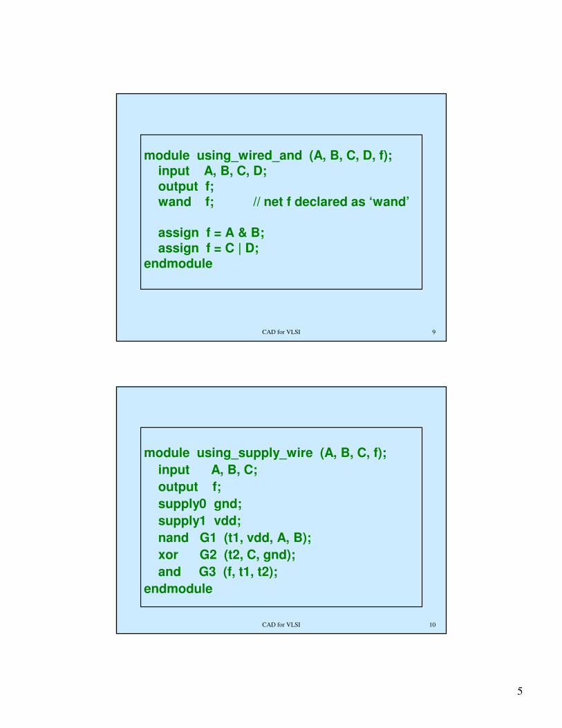
CAD for VLSI 35
module generate_mux (data, select, out);
input [0:7] data;
input [0:2] select;
output out;
assign out = data [select];
endmodule
Non-constant index in expression on RHS generates a MUX
CAD for VLSI 36
module generate_decoder (out, in, select);
input in;
input [0:1] select;
output [0:3] out;
assign out [select] = in;
endmodule
Non-constant index in expression on LHS generates a decoder

19
CAD for VLSI 37
module generate_set_of_MUX (a, b, f, sel);
input [0:3] a, b;
input sel;
output [0:3] f;
assign f = sel ? a : b;
endmodule
Conditional operatorgenerates a MUX
CAD for VLSI 38
module level_sensitive_latch (D, Q, En);
input D, En;
output Q;
assign Q = en ? D : Q;
endmodule
Using “assign” to describesequential logic

20
CAD for VLSI 39
Behavioral Style: Procedural Assignment
• The procedural block defines– A region of code containing sequential
statements.
– The statements execute in the order they are written.
• Two types of procedural blocks in Verilog– The “always” block
• A continuous loop that never terminates.
– The “initial” block
• Executed once at the beginning of simulation (used in Test-benches).
CAD for VLSI 40
• A module can contain any number of “always” blocks, all of which execute concurrently.
• Basic syntax of “always” block:
always @ (event_expression)begin
statement;
statement;end
• The @(event_expression) is required for both combinational and sequential logic descriptions.
Sequentialstatements

21
CAD for VLSI 41
• Only “reg” type variables can be assigned within an “always” block.
CAD for VLSI 42
Sequential Statements in Verilog1. begin
sequential_statementsend
2. if (expression)sequential_statement
[elsesequential_statement]
3. case (expression)expr: sequential_statement…….default: sequential_statement
endcase
begin...end not required
if there is only 1 stmt.

22
CAD for VLSI 43
4. forever
sequential_statement
5. repeat (expression)
sequential_statement
6. while (expression)
sequential_statement
7. for (expr1; expr2; expr3)
sequential_statement
CAD for VLSI 44
8. # (time_value)
• Makes a block suspend for “time_value” time units.
9. @ (event_expression)
• Makes a block suspend until event_expression triggers.

23
CAD for VLSI 45
// A combinational logic example
module mux21 (in1, in0, s, f);input in1, in0, s;output f;reg f;
always @ (in1 or in0 or s)if (s)
f = in1;else
f = in0;endmodule
CAD for VLSI 46
// A sequential logic example
module dff_negedge (D, clock, Q, Qbar);
input D, clock;
output Q, Qbar;
reg Q, Qbar;
always @ (negedge clock)
begin
Q = D;
Qbar = ~D;
end
endmodule
24
CAD for VLSI 47
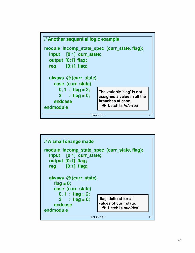
// Another sequential logic example
module incomp_state_spec (curr_state, flag);
input [0:1] curr_state;
output [0:1] flag;
reg [0:1] flag;
always @ (curr_state)
case (curr_state)
0, 1 : flag = 2;
3 : flag = 0;
endcase
endmodule
The variable ‘flag’ is not assigned a value in all thebranches of case.���� Latch is inferred
CAD for VLSI 48
// A small change made
module incomp_state_spec (curr_state, flag);input [0:1] curr_state;output [0:1] flag;reg [0:1] flag;
always @ (curr_state)flag = 0;case (curr_state)
0, 1 : flag = 2;3 : flag = 0;
endcaseendmodule
‘flag’ defined for allvalues of curr_state.���� Latch is avoided
25
CAD for VLSI 49
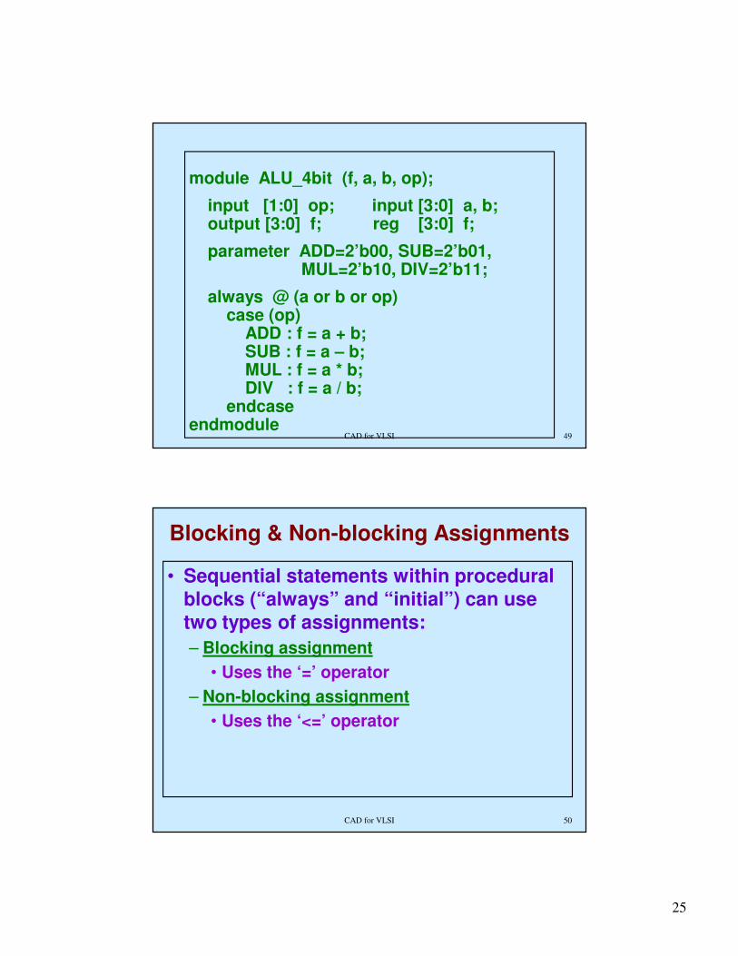
module ALU_4bit (f, a, b, op);
input [1:0] op; input [3:0] a, b;output [3:0] f; reg [3:0] f;
parameter ADD=2’b00, SUB=2’b01,MUL=2’b10, DIV=2’b11;
always @ (a or b or op)case (op)
ADD : f = a + b;SUB : f = a – b;MUL : f = a * b;DIV : f = a / b;
endcaseendmodule
CAD for VLSI 50
Blocking & Non-blocking Assignments
• Sequential statements within procedural blocks (“always” and “initial”) can use two types of assignments:
– Blocking assignment
• Uses the ‘=’ operator
– Non-blocking assignment
• Uses the ‘<=’ operator

26
CAD for VLSI 51
Blocking Assignment (using ‘=’)
• Most commonly used type.
• The target of assignment gets updated before the next sequential statement in the procedural block is executed.
• A statement using blocking assignment blocks the execution of the statements following it, until it gets completed.
• Recommended style for modeling combinational logic.
CAD for VLSI 52
Non-Blocking Assignment (using ‘<=’)
• The assignment to the target gets scheduled for the end of the simulation cycle.
– Normally occurs at the end of the sequential block.
– Statements subsequent to the instruction under consideration are not blocked by the assignment.
• Recommended style for modeling sequential logic.
– Can be used to assign several ‘reg’ type variables synchronously, under the control of a common clock.

27
CAD for VLSI 53
Some Rules to be Followed
• Verilog synthesizer ignores the delays specified in a procedural assignment statement.
• A variable cannot appear as the target of both a blocking and a non-blocking assignment.
– Following is not permissible:
value = value + 1;
value <= init;
CAD for VLSI 54
// Up-down counter (synchronous clear)
module counter (mode, clr, ld, d_in, clk, count);input mode, clr, ld, clk; input [0:7] d_in;output [0:7] count; reg [0:7] count;always @ (posedge clk)
if (ld)count <= d_in;
else if (clr)count <= 0;
else if (mode)count <= count + 1;
elsecount <= count + 1;
endmodule

28
CAD for VLSI 55
// Parameterized design:: an N-bit counter
module counter (clear, clock, count);parameter N = 7;input clear, clock; output [0:N] count; reg [0:N] count;
always @ (negedge clock)if (clear)
count <= 0;else
count <= count + 1;endmodule
CAD for VLSI 56
// Using more than one clocks in a module
module multiple_clk (clk1, clk2, a, b, c, f1, f2);
input clk1, clk2, a, b, c;
output f1, f2;
reg f1, f2;
always @ (posedge clk1)
f1 <= a & b;
always @ (negedge clk2)
f2 <= b ^ c;
endmodule

29
CAD for VLSI 57
// Using multiple edges of the same clock
module multi_phase_clk (a, b, f, clk);
input a, b, clk;
output f;
reg f, t;
always @ (posedge clk)
f <= t & b;
always @ (negedge clk)
t <= a | b;
endmodule
CAD for VLSI 58
A Ring Counter Example
module ring_counter (clk, init, count);input clk, init; output [7:0] count;reg [7:0] count;always @ (posedge clk)begin
if (init)count = 8’b10000000;
else begincount = count << 1;count[0] = count[7];
endend
endmodule
×

30
CAD for VLSI 59
A Ring Counter Example (Modified)
module ring_counter_modi1 (clk, init, count);input clk, init; output [7:0] count;reg [7:0] count;always @ (posedge clk)begin
if (init)count = 8’b10000000;
else begincount <= count << 1;count[0] <= count[7];
endend
endmodule
CAD for VLSI 60
About “Loop” Statements
• Verilog supports four types of loops:
– ‘while’ loop
– ‘for’ loop
– ‘forever’ loop
– ‘repeat’ loop
• Many Verilog synthesizers supports only ‘for’ loop for synthesis:
– Loop bound must evaluate to a constant.
– Implemented by unrolling the ‘for’ loop, and replicating the statements.
31
CAD for VLSI 61
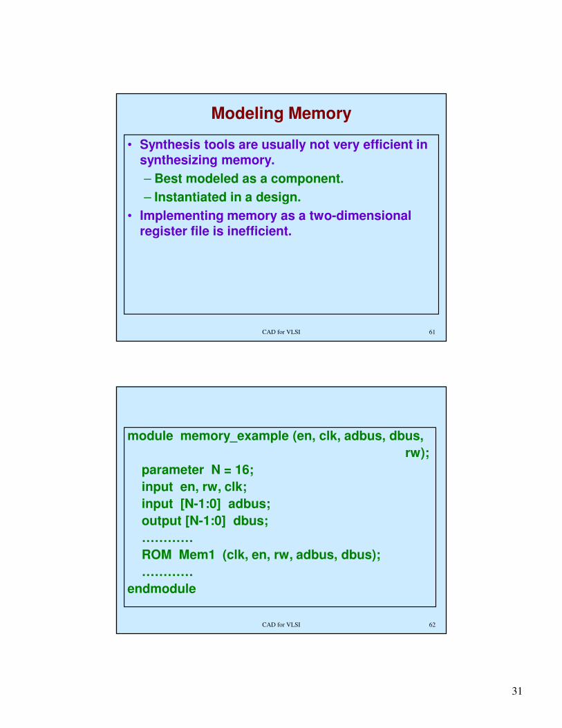
Modeling Memory
• Synthesis tools are usually not very efficient in synthesizing memory.
– Best modeled as a component.
– Instantiated in a design.
• Implementing memory as a two-dimensional register file is inefficient.
CAD for VLSI 62
module memory_example (en, clk, adbus, dbus,
rw);
parameter N = 16;
input en, rw, clk;
input [N-1:0] adbus;
output [N-1:0] dbus;
…………
ROM Mem1 (clk, en, rw, adbus, dbus);
…………
endmodule

32
CAD for VLSI 63
Modeling Tri-state Gates
module bus_driver (in, out, enable);
input enable; input [0:7] in;
output [0:7] out; reg [0:7] out;
always @ (enable or in)
if (enable)
out = in;
else
out = 8’bz;
endmodule;
CAD for VLSI 64
• Two types of FSMs
– Moore Machine
– Mealy Machine
Modeling Finite State Machines
NSLogic
F/FO/p
Logic
PSNS
NSLogic
F/FO/p
LogicPS
NS

33
CAD for VLSI 65
Moore Machine : Example 1
• Traffic Light Controller
– Simplifying assumptions made
– Three lights only (RED, GREEN, YELLOW)
– The lights glow cyclically at a fixed rate
• Say, 10 seconds each
• The circuit will be driven by a clock of appropriate frequency
clkRED
GREEN
YELLOW
CAD for VLSI 66
module traffic_light (clk, light);
input clk;
output [0:2] light; reg [0:2] light;
parameter S0=0, S1=1, S2=2;
parameter RED=3’b100, GREEN=3’b010,
YELLOW=3’b001;
reg [0:1] state;
always @ (posedge clk)
case (state)
S0: begin // S0 means RED
light <= YELLOW;
state <= S1;
end

34
CAD for VLSI 67
S1: begin // S1 means YELLOWlight <= GREEN;state <= S2;
endS2: begin // S2 means GREEN
light <= RED;state <= S0;
enddefault: begin
light <= RED;state <= S0;
endendcase
endmodule
CAD for VLSI 68
• Comment on the solution
– Five flip-flops are synthesized
• Two for ‘state’
• Three for ‘light’ (outputs are also latched into flip-flops)
– If we want non-latched outputs, we have to modify the Verilog code.
• Assignment to ‘light’ made in a separate ‘always’ block.
• Use blocking assignment.

35
CAD for VLSI 69
module traffic_light_nonlatched_op (clk, light);input clk;output [0:2] light; reg [0:2] light;parameter S0=0, S1=1, S2=2;parameter RED=3’b100, GREEN=3’b010,
YELLOW=3’b001;reg [0:1] state;always @ (posedge clk)
case (state)S0: state <= S1;S1: state <= S2;S2: state <= S0;default: state <= S0;
endcase
CAD for VLSI 70
always @ (state)
case (state)
S0: light = RED;
S1: light = YELLOW;
S2: light = GREEN;
default: light = RED;
endcase
endmodule

36
CAD for VLSI 71
Moore Machine: Example 2
• Serial parity detector
x
clkz
EVEN ODD
x=1x=0 x=0
x=1
= 0, for even
1, for odd
CAD for VLSI 72
module parity_gen (x, clk, z);
input x, clk;
output z; reg z;
reg even_odd; // The machine state
parameter EVEN=0, ODD=1;
always @ (posedge clk)
case (even_odd)
EVEN: begin
z <= x ? 1 : 0;
even_odd <= x ? ODD : EVEN;
end
37
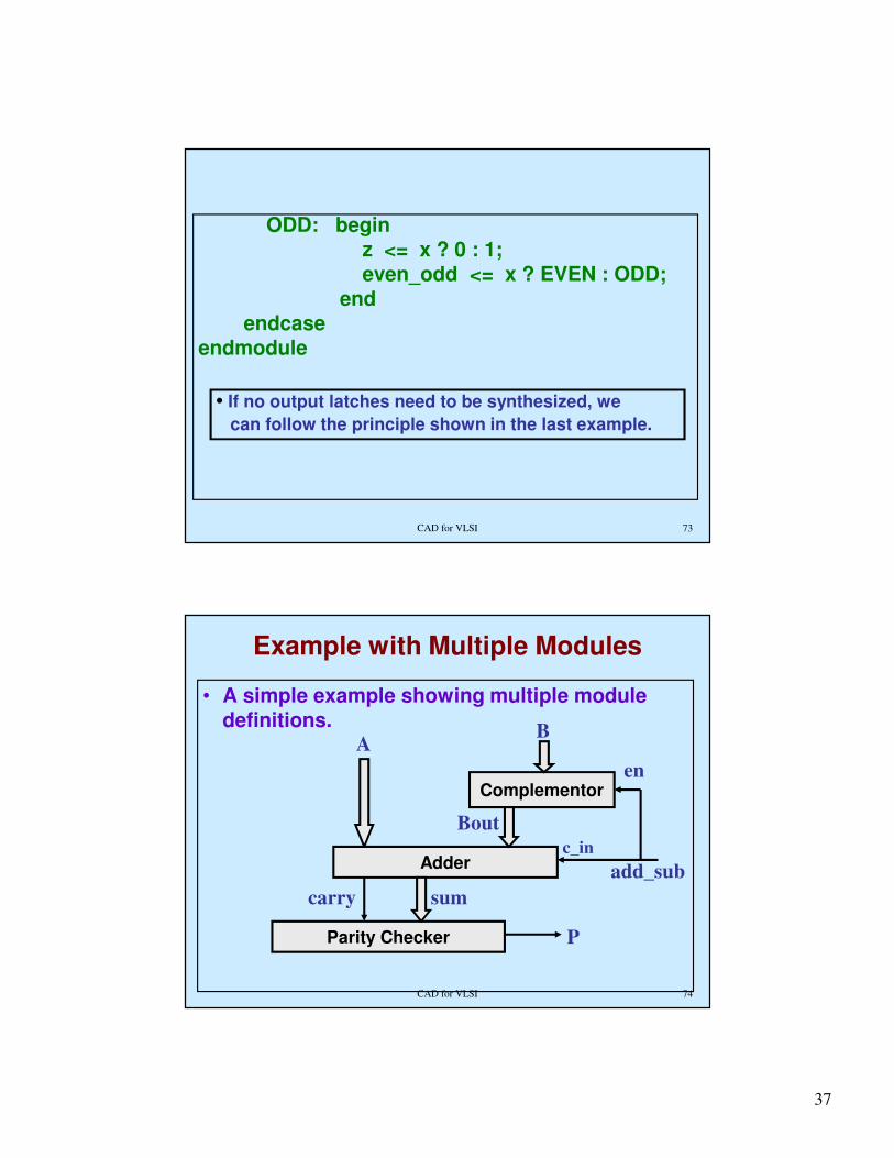
CAD for VLSI 73
ODD: beginz <= x ? 0 : 1;even_odd <= x ? EVEN : ODD;
endendcase
endmodule
• If no output latches need to be synthesized, we
can follow the principle shown in the last example.
CAD for VLSI 74
Example with Multiple Modules
• A simple example showing multiple module definitions.
Complementor
Adder
Parity Checker P
AB
add_sub
Bout
sumcarry
en
c_in
38
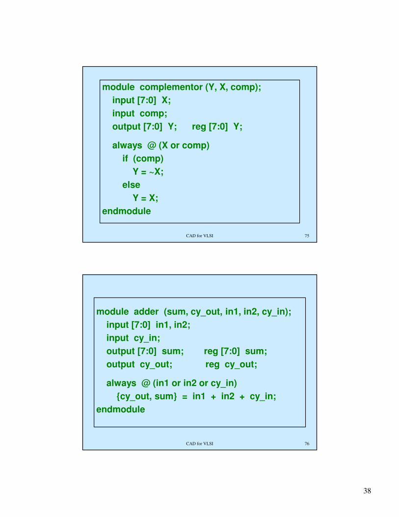
CAD for VLSI 75
module complementor (Y, X, comp);
input [7:0] X;
input comp;
output [7:0] Y; reg [7:0] Y;
always @ (X or comp)
if (comp)
Y = ~X;
else
Y = X;
endmodule
CAD for VLSI 76
module adder (sum, cy_out, in1, in2, cy_in);
input [7:0] in1, in2;
input cy_in;
output [7:0] sum; reg [7:0] sum;
output cy_out; reg cy_out;
always @ (in1 or in2 or cy_in)
{cy_out, sum} = in1 + in2 + cy_in;
endmodule

39
CAD for VLSI 77
module parity_checker (out_par, in_word);
input [8:0] in_word;
output out_par;
always @ (in_word)
out_par = ^ (in_word);
endmodule
CAD for VLSI 78
// Top level module
module add_sub_parity (p, a, b, add_sub);
input [7:0] a, b;
input add_sub; // 0 for add, 1 for subtract
output p; // parity of the result
wire [7:0] Bout, sum; wire carry;
complementor M1 (Bout, B, add_sub);
adder M2 (sum, carry, A, Bout, add_sub);
parity_checker M3 (p, {carry, sum});
endmodule

40
CAD for VLSI 79
Verilog Test Bench
CAD for VLSI 80
Introduction
• What is test bench?
– A Verilog procedural block which executes only once.
– Used for simulation.
– Testbench generates clock, reset, and the required test vectors.

41
CAD for VLSI 81
ModuleUnderTest
Test Bench
Comparelogic
Stimulus
CAD for VLSI 82
How to Write Testbench?
• Create a dummy template– Declare inputs to the module-under-test (MUT)
as “reg”, and the outputs as “wire”.
– Instantiate the MUT.
• Initialization– Assign some known values to the MUT inputs.
• Clock generation logic– Various ways to do so.
• May include several simulator directives– Like $display, $monitor, $dumpfile,
$dumpvars, $finish.

42
CAD for VLSI 83
• $display– Prints text or variables to stdout.
– Syntax same as “printf”.
• $monitor– Similar to $display, but prints the value whenever
the value of some variable in the given list changes.
• $finish– Terminates the simulation process.
• $dumpfile– Specify the file that will be used for storing the
waveform.
• $dumpvars– Starts dumping all the signals to the specified file.
CAD for VLSI 84
Example Test Bench
module shifter_toplevel;
reg clk, clear, shift;
wire [7:0] data;
shift_register S1 (clk, clear, shift, data);
initial
begin
clk = 0; clear = 0; shift = 0;
end
always
#10 clk = !clk;
endmodule

43
CAD for VLSI 85
Test Bench: More Complete Version
module shifter_toplevel;
reg clk, clear, shift;
wire [7:0] data;
shift_register S1 (clk, clear, shift, data);
initial
begin
clk = 0; clear = 0; shift = 0;
end
always
#10 clk = !clk;
contd..
CAD for VLSI 86
initial
begin
$dumpfile (“shifter.vcd”);
$dumpvars;
end
initial
begin
$display (“\ttime, \tclk, \tclr, \tsft, \tdata);
$monitor (“%d, %d, %d, %d, %d”, $time,
clk, reset, clear, shift, data);
end
initial
#400 $finish;
***** REMAINING CODE HERE ******
endmodule

44
CAD for VLSI 87
A Complete Example
module testbench;
wire w1, w2, w3;
xyz m1 (w1, w2, w3);
test_xyz m2 (w1, w2, w3);
endmodule
module xyz (f, A, B);
input A, B; output f;
nor #1 (f, A, B);
endmodule
contd..
CAD for VLSI 88
module test_xyz (f, A, B);
input f;
output A, B;
reg A, B;
initial
begin
$monitor ($time, “A=%b”, “B=%b”, f=%b”,
A, B, f);
#10 A = 0; B = 0;
#10 A = 1; B = 0;
#10 A = 1; B = 1;
#10 $finish;
end
endmodule

45
CAD for VLSI 89
Pipelining Example
• Consider the following arithmetic computation:
X = (A + B) * (B – C + D)
Y = (B – C + D)
• Suppose we break into three stages:
– S1: S1_T1 = A+B; S1_T2 = B-C; S1_T3 = D;
– S2: S2_T1 = S1_T1; S2_T4 = S1_T2 + S1_T3;
– S3: S3_X = S2_T1 * S2_T4; S3_Y = S2_T4;
CAD for VLSI 90
module pipeline_example (A, B, C, D, X, Y, clk);
input [0:7] A, B, C, D, clk;
output X, Y;
wire [0:18] X; wire [0:9] Y;
reg [0:8] S1_T1, S2_T1, S1_T2;
reg [0:7] S1_T3; reg [0:9] S2_T4, S3_Y; reg [0:18] S3_X;
assign X = S3_X; assign Y = S3_Y;
always @(posedge clk)
begin
S1_T1 <= A + B; S1_T2 <= B – C; S1_T3 <= D;
S2_T1 <= S1_T1; S2_T4 <= S1_T2 + S1_T3;
S3_X <= S2_T1 * S2_T4; S3_Y <= S2_T4;
end;
endmodule