Embed Size (px)
Citation preview

Verilog HDL Implementation of a Universal
Synchronous Asynchronous Receiver Transmitter
Jefferson Hora, Meriam Gay Bautista, Kramer C. Chua, and Demie Mae V. Dajao Microelectronics Lab, EECE Department MSU-Iligan Institute of Technology, Iligan City, Philippines
Email: [email protected],edu.ph, [email protected], [email protected],
Abstract—This paper presents the Verilog HDL
implementation of a Universal Synchronous/ Asynchronous
Receiver/Transmitter (USART). The proposed design
exhibits enhance power efficiency compared to the standard
USART 8251a, which dissipates 48.2462 μW. To make the
USART more power efficient, the basic block and pins for
mode and control instructions had been modified so that the
individual blocks were only activated when each had a
certain function to execute. The standard function of a
USART is implemented in the researcher’s design, being
able to do Serial-to-Parallel and Parallel-to-Serial data
conversion and have both synchronous and asynchronous
modes. The total chip area is 2046.05682µm2.
Index Terms—asynchronous communication, data
transmission, parallel communication, peripheral, RS 232,
serial communication, synchronous communication, verilog
HDL
I. INTRODUCTION
For many years, serial port has been an integral part of
most computer operating systems in use today and has
been considered to be one of the most basic external
connections in the computer. [1]
Basically, serial ports provide a standard connector and
protocol to let you attach devices, such as modems in the
computer. The advantage of using a serial port is that it
needs only one wire to transmit the 8 bits of the byte
compared to a parallel port which needs 8 wires. In
addition, serial ports have less cable components thus it
has lower cost.
Serial ports rely on a special controller chip called
Universal Asynchronous Receiver/Transmitter (UART).
UART is responsible for performing the main task in
serial communications in computers. It is an integrated
circuit, which is used for transmitting and receiving data
asynchronously via the serial port on the computer. It
contains a parallel-to-serial converter for data transmitted
from the computer and a serial-to-parallel converter for
data coming in via the serial line. [2]
The same way with UART, a Universal Synchronous
Asynchronous Receiver Transmitter (USART) provides
the computer with the interface necessary for
Manuscript received December 5, 2013; accepted March 1, 2014. This research is under the support of Engineering Research
Development and Technology, Department of Science and Technology.
communication with modems and other serial devices.
However, a USART offers the option of synchronous
mode. The USART even though with all of its
capabilities should also be able to perform with high
efficiently especially when using it on real world
applications. [3]
One of the things to consider on microelectronic when
it comes to performance and longevity of the device is its
power consumption. Bigger power consumption results
on higher operating temperature which would result on
faster degradation of our components.
This paper presents the design and implementation of a
low power Universal Synchronous Asynchronous
Receiver Transmitter (USART). By modifying the basic
block and pins for mode and control instructions so that
the individual blocks were only activated when each had
a certain function to fulfill. Major considerations in the
design and implementation of this USART will be to
obtain its desired ability to transmit and received data
both through asynchronous and synchronous transmission
all the while with lower power consumption.
II. ARCHITECTURE
A. Standard USART Block Module
A standard USART is usually composed of 26 I/O pins,
shown in Fig. 1. A set of mode instructions must be sent
out by the CPU and received through the 8251A Data
Bus that initializes the 8251A to support the desired
communications format.
Figure 1. Standard USART block module
International Journal of Electronics and Electrical Engineering Vol. 2, No. 4, December, 2014
©2014 Engineering and Technology Publishing 264doi: 10.12720/ijeee.2.4.264-269

The 8251A also has a set of modem control inputs and
outputs that can be used to simplify the interface to
almost any modem. For transmission, the parallel data
enters to the USART through the Data Bus, converted to
serial data and then shifted out to the TxD pin. For
reception, the serial data enters to the USART through
the RxD pin, converted to parallel data and then shifted
out to the Data Bus. [4]
B. Proposed USART Block Module
Fig. 2 and Table I shows the proposed USART block
module and its pins description. It is consist of 24 I/O
pins.
Figure 2. Block module of the proposed USART
TABLE I. PROPOSED USART PIN NAMES AND DESCRIPTION
C. Flow of Operation
Fig. 3 shows the overall system diagram of the
USART. The Data Bus is responsible for receiving and
transmitting data straight from the CPU.
Figure 3. USART overall system diagram
The Tx block manages all activities associated with the
transmission of serial data. It also accepts parallel data
from the Data Bus, converts it to a serial bit stream and
outputs a composite serial stream of data on to the
modem.
The Rx block manages all receiver-related activities. It
also accepts serial data, converts this serial input to
parallel format, and sends this assembled character to the
CPU through the Data Bus.
Fig. 4 and Fig. 5 shows the blocks that were activated
during reception and transmission of data. To minimize
power, the Tx block and Rx blocks were not activated
when not used, they remain in the idle state when they
don’t have to transmit and receive respectively. The Tx
block and Rx block were both separated, which means
that the Rx block is only activated when data was
received and the Tx Block was only activated when data
was transmitted.
Figure 4. Blocks activated when receiving data
Figure 5. Blocks activated when transmitting data
Fig. 6 shows the flow of operation of the USART.
Prior to start data transmission or reception, the USART
International Journal of Electronics and Electrical Engineering Vol. 2, No. 4, December, 2014
©2014 Engineering and Technology Publishing 265

was loaded with a set of control wordsgenerated by the
CPU.These control signals define the complete functional
definition of the USART. The control words were
referred to as the Mode.
Figure 6. Flow of operation
Once the Mode Instruction has been written into the
USART by the CPU, SYNC character/s (for synchronous
mode only) or data (8-bit) has been written. To return to
the Mode Instruction format (to switch from
asynchronous mode to synchronous mode, vice versa),
the Reset pin can be set to initiate a reset operation which
will automatically places USART back into the Mode
Instruction Format. The second sync character was
skipped when the mode instruction has programmed the
USART to single character sync mode. Both sync
characters were skipped when the mode instruction has
programmed the USART to async mode.
D. Mode of Instruction
The USART was used for either Asynchronous or
Synchronous data communication. The CPU sent the
USART Mode Instructions and determined the kind of
data communication used by the USART. The Mode
Instruction consisted of two input pins namely,
comm_type pin and sync_type pin. These two pins
indicated if the USART used Asynchronous or
Synchronous mode and how many sync characters to be
used for Synchronous Mode. Table II shows the different
Mode Instruction for different input of comm_type pin
and sync_type pins.
Modifying the mode of instructions was used also
contributed to the reduction of power consumption.
Instead of the conventional way of using 8 data bits of
character to load onto the USART, three pins were
dedicated into determining what mode the USART
should be used
TABLE II. MODE OF INSTRUCTIONS
Comm_type Sync_type ModeInstruction
0 -- Async mode
1 0 Sync mode
1 1 Sync mode
(2 sync char)
III. SIMULATION RESULTS
Simulation results and chip implementation of this
design is carried out by Xilinx Design Tool and Synopsys
Digital Platform.
A. Transmitter Asynchronousand Synchronous
Fig. 7 below shows the simulation waveform of the
USART’s Transmitter Asynchronous function. Prior to
the starting data transmission, the reset pin was set to its
negative edge which activated the USART. Once the
USART was activated, the transmitter asynchronous
mode was set by providing a low input comm_type pin. A
“high” on the “wr (write)” input pin on every positive
edge of the clock indicated that the CPU was writing data
into the USART which will be transmitted into the
modem.
The CPU then wrote the parallel data into the USART
through the Data_Bus and that parallel data was then
converted into serial data before being shifted out in the
TxD pin to the modem. In this transmission, the data in
by the CPU was 01010101. A “high” in Byte_ready
informed the USART that the data was ready to be
transmitted. Then the USART started transmitting data
into the modem when the Tx_start pin was set to high.
The data 01010101 was then shifted out to the TxD pin to
the modem starting with the Start bit, then LSB, to MSB,
of the data, and lastly the Stop bit. When there are no data
characters to be transmitted, the TxD output remains
“high” unless there were new data to be sent. Clear to
send (CTS), DSR and Data Terminal Ready (DTR) pins,
are for modem control of USART.
Figure 7. Transmitter asynchronous
Fig. 8 shows the simulation result for Transmitter
Synchronous function of the USART. Prior to starting
data transmission, reset_ pin was set to negative edge
which activated the USART. The comm_type pin was set
to high to achieve synchronous mode. In this synchronous
transmission sync_type was “low” which meant that 1
sync character will be used. Next, a “high” of wr input
pin every positive edge indicated that the CPU was
writing data into the USART and this data was set to be
transmitted into the modem. After the mode was set, 1
synchronous character was sent by the CPU through the
Data_Bus and was stored in one of the registers inside the
USART. For this transmission, the synchronous character
was 10101010.
After synchronous character has been written, the CPU
then wrote the parallel data into the USART through the
Data_Bus. The parallel data was converted to serial data
before being shifted out in the TxD pin then into the
International Journal of Electronics and Electrical Engineering Vol. 2, No. 4, December, 2014
©2014 Engineering and Technology Publishing 266
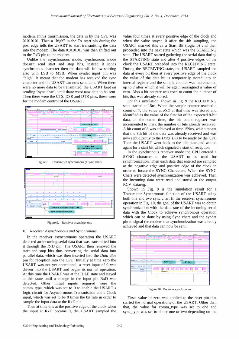
modem. Inthis transmission, the data in by the CPU was
01010101. Then a “high” in the Tx_start pin during the
pos. edge tells the USART to start transmitting the data
into the modem. The data 01010101 was then shifted out
to the TxD pin to the modem.
Unlike the asynchronous mode, synchronous mode
doesn’t send start and stop bits, instead it sends
synchronous character then the data will follow starting
also with LSB to MSB. When syndet input pin was
“high”, it meant that the modem has received the sync
character and the USART can now send data. When there
were no more data to be transmitted, the USART kept on
sending “sync char”, until there were new data to be sent.
Then there were the CTS, DSR and DTR pins, these were
for the modem control of the USART.
Figure 8. Transmitter synchronous (1 sync char)
Figure 9. Receiver asynchronous
B. Receiver Asynchronous and Synchronous
In the receiver asynchronous operation the USART
detected an incoming serial data that was transmitted into
it through the RxD pin. The USART then removed the
start and stop bits thus converting the serial data into
parallel data, which was then inserted into the Data_Bus
pin for reception into the CPU. Initially at time zero the
USART was not yet operational, a reset input of 0 was
driven into the USART and began its normal operation.
At this time the USART was at the IDLE state and stayed
at this state until a change in the input pin RxD was
detected. Other initial inputs required were the
comm_type, which was set to 0 to enable the USART’s
logic circuit for Asynchronous Transmission and a Clock
input, which was set to be 8 times the bit rate in order to
sample the input data at the RxD pin.
Then at time 6ns at the positive edge of the clock when
the input at RxD became 0, the USART sampled the
value four times at every positive edge of the clock and
when the value stayed 0 after the 4th sampling, the
USART marked this as a Start Bit (logic 0) and then
proceeded into the next state which was the STARTING
state. The USART started gathering the serial data during
the STARTING state and after 4 positive edges of the
clock the USART preceded into the RECEIVING state.
During the RECEIVING state, the USART sampled the
data at every bit then at every positive edge of the clock
the value of the data bit is temporarily stored into an
internal register and the sample counter was incremented
up to 7 after which it will be again reassigned a value of
zero. Also a bit counter was used to count the number of
bits that was already stored.
For this simulation, shown in Fig. 9 the RECEIVING
state started at 15ns. When the sample counter reached a
count of 7, the value at RxD at that time was stored and
identified as the value of the first bit of the expected 8-bit
data, at the same time, the bit count register was
incremented to mark the number of bits already received.
A bit count of 8 was achieved at time 159ns, which meant
that the 8th bit of the data was already received and was
now sent directly to the Data_Bus to be ready by the CPU.
Then the USART went back to the idle state and waited
again for a start bit which signaled a start of reception.
In the synchronous receiver mode the CPU entered a
SYNC character to the USART to be used for
synchronization. Then each data that entered are sampled
at the negative edge and positive edge of the clock in
order to locate the SYNC Characters. When the SYNC
Chars were detected synchronization was achieved. Then
the incoming data were read and stored at the output
RCV_datareg.
Shown in Fig. 8 is the simulation result for a
Transmitter Synchronous function of the USART using
both one and two sync char. In the receiver synchronous
operation in Fig. 10, the goal of the USART was to obtain
synchronization with the data rate of the incoming serial
data with the Clock to achieve synchronous operation
which can be done by using Sync chars and the syndet
pin to signal the modem that synchronization was already
achieved and that data can now be sent.
Figure 10. Receiver synchronous
Firsta value of zero was applied to the reset pin that
started the normal operations of the USART. Other than
that, the value for comm_type was set to one and
sync_type was set to either one or two depending on the
International Journal of Electronics and Electrical Engineering Vol. 2, No. 4, December, 2014
©2014 Engineering and Technology Publishing 267

desired number of sync characters to use. Simultaneously
the CTS modem control output signaled the modem to
start its transmission of data into the USART.
The USART would require the CPU to determine what
the value of the SYNC character to use; this was done by
using the wr command
Every neg. edge of the clock and the value of the wr
command was zero, the data inputs on the Data_Bus was
used as the Sync Character. After the Sync Characters
were determined, the USART proceeded into the
HUNT_SYNC state where it searched for Sync
Characters until it achieved synchronization. Before
being able to hunt for these characters, a signal was
asserted to the hunt_sync pin of the USART after that, it
started to hunt for sync characters. At the test bench, it
shows that the hunt_sync was asserted during time 100ns.
Then, the USART sampled the values during the
negative edge and positive edge of the clock and checked
if they were equal and compared it to the LSB of the
chosen sync character. When both values were the same
the USART then proceeded with the next negative edge
and positive edge of the clock and saw that the values
were still the same and compared them again if it had the
same value with the next bit of the chosen sync char. This
went on until the time came that the USART had detected
an input with the same value with the Sync char and
synchronized with the clock.
After this, the USART was at the RECEIVING state.
And a syndet signal wasasserted and sent into the Modem
to signal it that Synchronization was achieved and that it
could send data into the USART. During this stage the
data was sampled during each positive edge of the clock
and this value was stored to a registered until 8bits were
compiled before being sent to the Data_Bus for the CPU
to read.
IV. IC COMPILER RESULT
Table III shows the power consumption of the USART.
The total dynamic power of the integrated circuit was
48.2462 uW. The cell internal power and net switching
power were 25.9006 uW and 22.3456 uW. Since the
dynamic power was small, once the device operated, it
consumed less power and it did not heat up easily. It
wasalso showed that the cell leakage power wass 9.7455
uW, it was the power consumed by a gate when it is not
switched, as well as the glitches in the system.
TABLE III. POWER CONSUMPTION OF USART
Report: Power Analysis
Design USART
Global Operating Voltage 1.08 V
Power Specific Unit Information
Voltage units 1 V
Capacitance Unit 1.00000pf
Time Units 1 ns
Dynamic Power Units 1 mW
Leakage Power Units 1 pW
Cell Internal power 25.9006 uW (54%)
Net Switching Power 22.3456 uW (46%)
Total Dynamic Power 4802462 uW (100%)
Table IV shows that the total area of the integrated
circuit of USART was 2046.056820um2 while the total
cell area of the integrated circuit of LDPC decoder was
1769.750000um2.
TABLE IV. AREA PARAMETERS FOR THE USART
Report: Area Analysis
Design USART
No. of ports 27
No. of nets 48
No. of combinational cells 20
No. of buf/inv 12
No. of reference 8
Combinational Area 899.0 µm2
Noncombinational Area 870.75 µm2
Net Interconnect area 276.306820 µm2
Total cell area 1769.75 µm2
Total area 2046.056820 µm2
Figure 11. Chip level layout
Figure 12. Block level layout
Fig. 12 shows the BLOCK level layout for the USART.
Based on the figure shown, the integrated circuit had no
issue regarding congestion since it was well distributed
and only contained a low possibility of congestion which
means it did not heat up easily.
TABLE V. SUMMARY OF DESIGN SPECIFICATION
Parameters Design Specifications
Area 2046.0582 mm2
Power Dissipation 48.2462 uW
International Journal of Electronics and Electrical Engineering Vol. 2, No. 4, December, 2014
©2014 Engineering and Technology Publishing 268

V. CONCLUSION
A Universal Synchronous/Asynchronous
Receiver/Transmitter design with a lower power
consumption than the standard 1W voltage dissipation
has been presented in this paper. The fundamentals of
USART blocks and their operations were discussed on
the chapters of this paper. Thus, the conclusion and
analysis of this research were summarized as follows:
For USART reception process, the digital serial data
signal from the MODEM was first converted to parallel
data and was then shifted out at the positive edge of the
internal clock of the USART and was then received by
the CPU. As for the USART transmission process, the
parallel data from the CPU was converted into serial data
and was transmitted to the modem. The simulation results
show that the USART in this special project was working
properly on both receiver and transmitter functions since
the data was clearly seen to have been converted from
serial to parallel for the reception process and from
parallel to serial for the transmission process.
The simulation results also show that the synchronous
function of this paper’s USART has been working
properly since it was able to achieve synchronization with
the use of sync characters and at the same time, the
USART was still able to perform its other basic functions.
Also, this paper’s USART was able to achieve lower
power dissipation compared to other commercial ADCs
existing in the market. Hence, the researchers conclude
that the primary objectives of this paper have been
considerately met.
ACKNOWLEDGMENT
The authors wish to thank DOST-ERDT Eye-C
Program for the research grant in providing the industry
standard IC design tools. Special thanks to Synopsys
engineers for the technical support.
REFERENCES
[1] Y. Jinhong and H. Yongqiang, “Design of UART based on
ARM+DSP distributed data acquisition system,” in Proc. 8th
International Conference on Electronic Measurement and Instruments, 2007, pp. 4-813-4-815.
[2] L. Dris and M. Y. Idna, “A VHDL implementation of BIST
technique in UART,” in Proc. Conference on Convergent Technologies for the Asia-Pacific Region, TENCON, vol. 4, 2003,
pp. 1450–1454.
[3] K. Joshi, D. Patel, C. Patel, and R. Kuhel, “Design and simulation of UART IP core for FPGA implementation,” in Proc. National
Conference on Recent Trends in Engineering & Technology, BVM
Engineering College, V.V. Nagar, Gujarat, India, May 2011. [4] J. Norhuzaimin and H. H. Maimum, “The design of high speed
UART,” in Proc. Asia-Pacific Conference on Applied
Electromagnetics, 2005.
Jefferson A. Hora received his bachelor degree in Electronics and Communications
Engineering from the Mindanao State
University-Iligan Institute of Technology (MSU-IIT), Philippines, in 2002 and his M.S. in
Electrical Engineering major in IC Design from
National Taipei University, Taiwan, in 2009. He has been an IC Design Engineer in Service
& Quality Technology Co.,Ltd, Taipei, Taiwan
from 2009-2010. Recently, a faculty member as Asst. Professor of MSU-IIT since 2010, and is a faculty affiliate and adviser of the
Microelectronics Laboratory. His research interest focuses in power
management IC, RF-DC converter, analog IC, FPGA design and prototype.
Meriam Gay Bautista received her bachelor degree in Electronics and Communications
Engineering from the Mindanao Sta te University-Iligan Institute of Technology
(MSU-IIT), Philippines, in 2008 and her M.S.
in Electrical Engineering major in IC Design from National Taipei University, Taiwan, in
2013. Recently, she is an Asst. Professor in the
Department of Electrical, Electronics and Computer Engineering in MSU-IIT. Her research interest includes
power electronics design, power management IC, DC-DC converter,
analog IC, LED Driver and FPGA design and Implementation.
Kramer C. Chua received her bachelor degree
in Electronics and Communications
Engineering from the Mindanao State University-Iligan Institute of Technology
(MSU-IIT), Philippines, in 2013
Demie Mae V. Dajao received her bachelor degree in Electronics and Communications
Engineering from the Mindanao State
University-Iligan Institute of Technology
(MSU-IIT), Philippines, in 2013
International Journal of Electronics and Electrical Engineering Vol. 2, No. 4, December, 2014
©2014 Engineering and Technology Publishing 269