Embed Size (px)
Citation preview

Verification of HBM through Direct Probing on MicroBumps
Marc LorangerFormFactor
Sung Wook MoonSK hynix
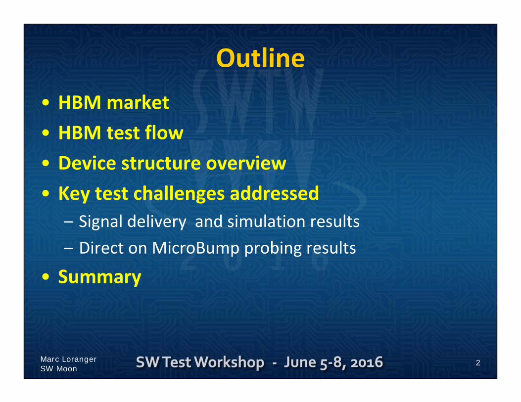
Outline• HBM market• HBM test flow • Device structure overview • Key test challenges addressed
– Signal delivery and simulation results– Direct on MicroBump probing results
• Summary
2Marc Loranger SW Moon
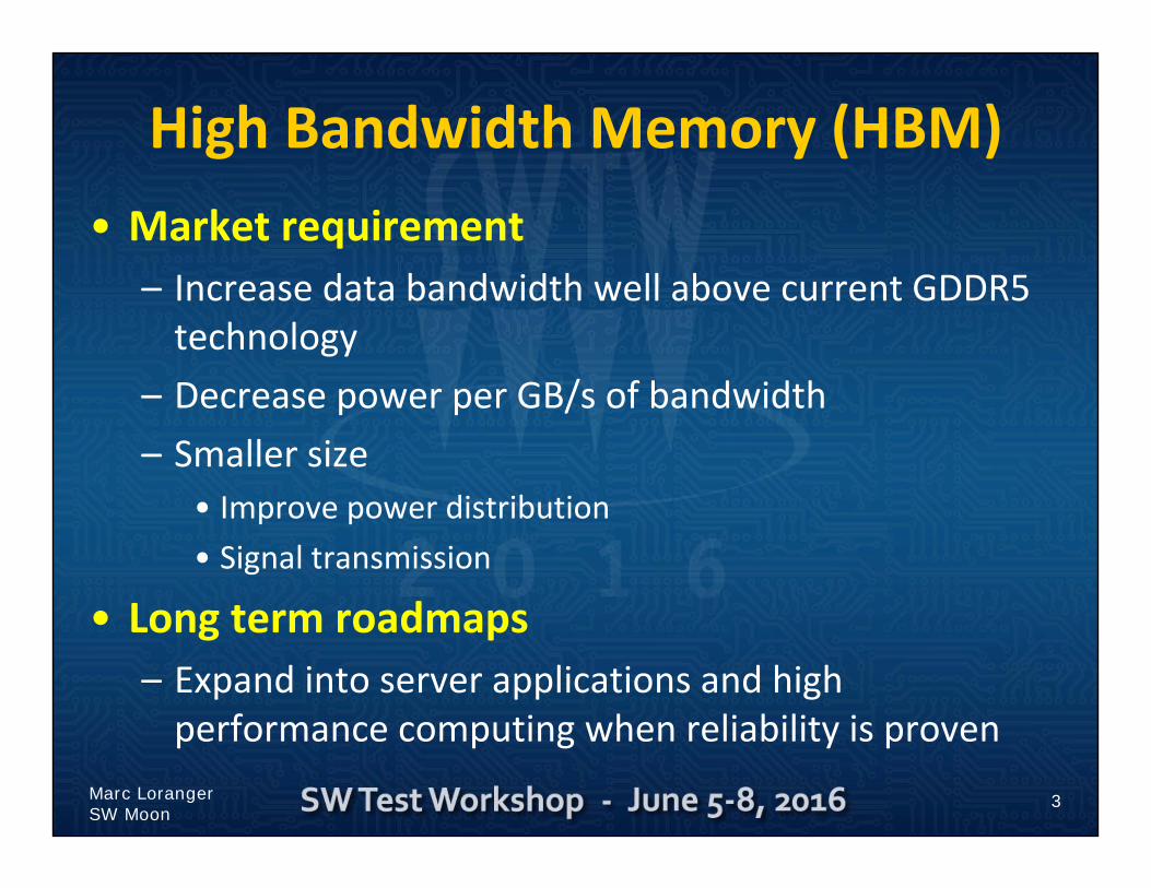
High Bandwidth Memory (HBM)• Market requirement
– Increase data bandwidth well above current GDDR5 technology
– Decrease power per GB/s of bandwidth– Smaller size
• Improve power distribution • Signal transmission
• Long term roadmaps– Expand into server applications and high performance computing when reliability is proven
3Marc Loranger SW Moon
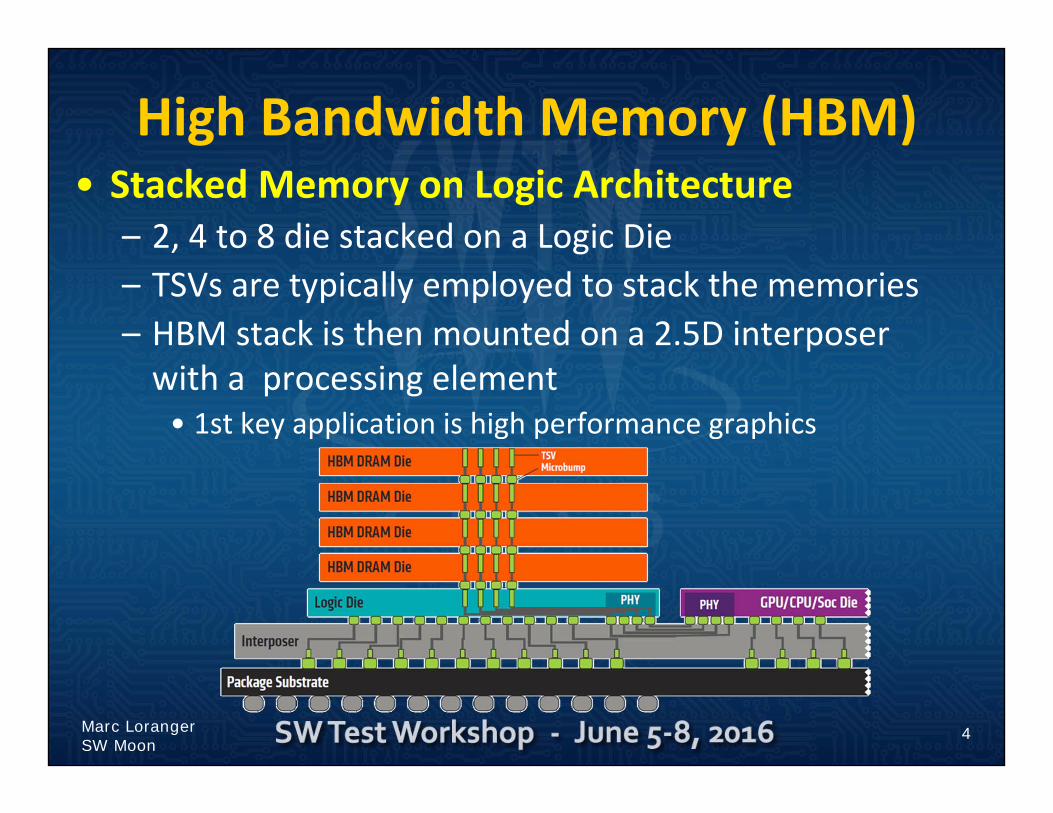
High Bandwidth Memory (HBM)• Stacked Memory on Logic Architecture
– 2, 4 to 8 die stacked on a Logic Die– TSVs are typically employed to stack the memories– HBM stack is then mounted on a 2.5D interposer with a processing element • 1st key application is high performance graphics
4Marc Loranger SW Moon
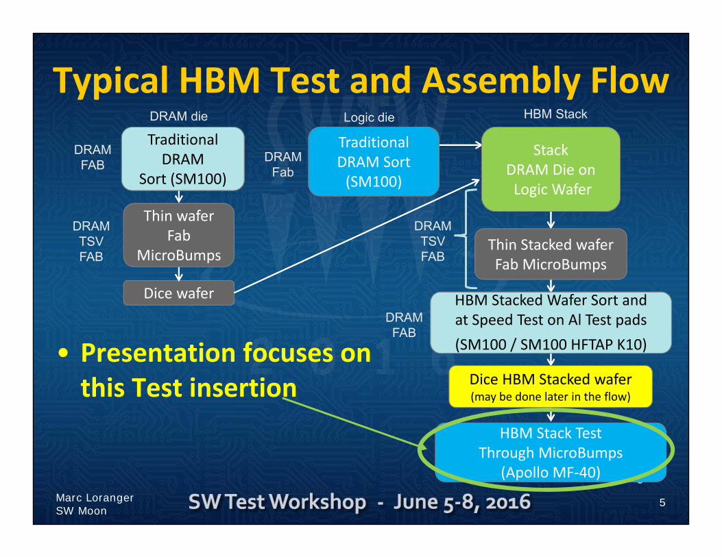
Typical HBM Test and Assembly Flow
5
DRAM die Logic die HBM Stack
DRAMFAB
DRAMTSVFAB
Dice wafer
Traditional DRAM Sort(SM100)
DRAMFab
DRAMTSVFAB
DRAMFAB
TraditionalDRAM
Sort (SM100)
Thin waferFab
MicroBumpsThin Stacked waferFab MicroBumps
StackDRAM Die on Logic Wafer
HBM Stacked Wafer Sort and at Speed Test on Al Test pads(SM100 / SM100 HFTAP K10)
Dice HBM Stacked wafer (may be done later in the flow)
HBM Stack TestThrough MicroBumps
(Apollo MF‐40)
• Presentation focuses on this Test insertion
Marc Loranger SW Moon
5

HBM 2 Direct Probe on Micro Bumps Requirement
• Array size– 6022µm x 2832µm
• Test requirement– 2.133 Gb/s Functional test of the stack
– All 8 device channels
• HBM Array Structure– Total TSV Micro Bumps: 3990
• 55µm Micro Bump Pitch– Total IO Micro Bumps: 1728– Direct access micro bumps 176– Total Power Supplies: 3 – 1056 – Total ground Micro Bumps: 1030
55µm Pitch
Marc Loranger SW Moon
I/O P
WR
PWR
Dire
ctA
cces
s
6
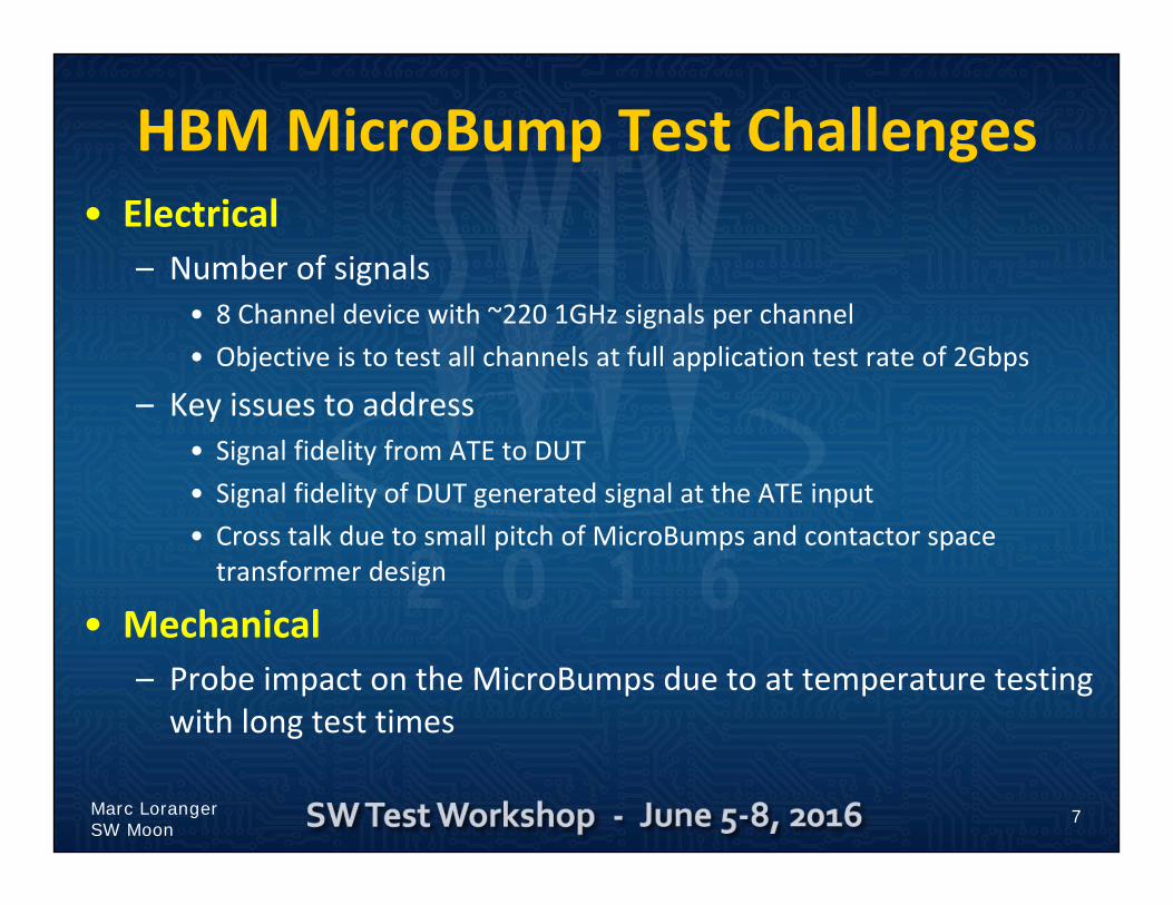
HBM MicroBump Test Challenges• Electrical
– Number of signals• 8 Channel device with ~220 1GHz signals per channel• Objective is to test all channels at full application test rate of 2Gbps
– Key issues to address• Signal fidelity from ATE to DUT• Signal fidelity of DUT generated signal at the ATE input• Cross talk due to small pitch of MicroBumps and contactor space transformer design
• Mechanical– Probe impact on the MicroBumps due to at temperature testing with long test times
7Marc Loranger SW Moon
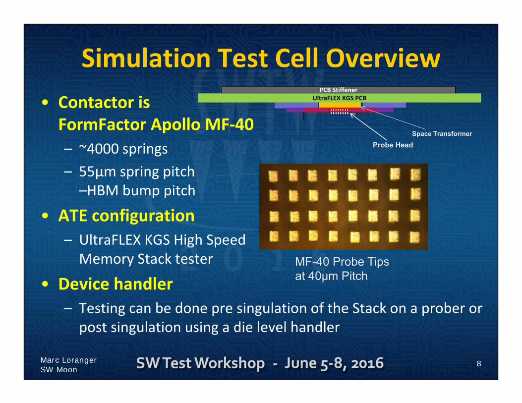
Simulation Test Cell Overview• Contactor is FormFactor Apollo MF‐40– ~4000 springs– 55µm spring pitch –HBM bump pitch
• ATE configuration– UltraFLEX KGS High SpeedMemory Stack tester
• Device handler– Testing can be done pre singulation of the Stack on a prober orpost singulation using a die level handler
8Marc Loranger SW Moon
PCB Stiffener
Space TransformerProbe Head
UltraFLEX KGS PCB
MF-40 Probe Tipsat 40µm Pitch
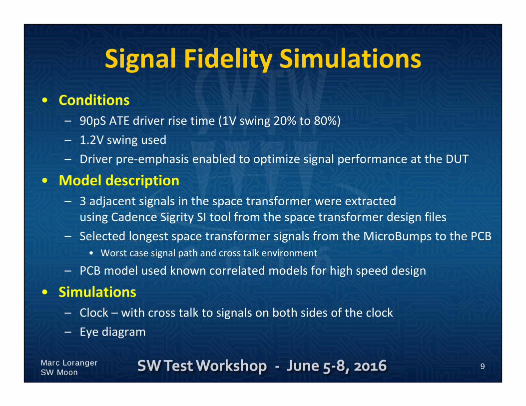
Signal Fidelity Simulations• Conditions
– 90pS ATE driver rise time (1V swing 20% to 80%)– 1.2V swing used– Driver pre‐emphasis enabled to optimize signal performance at the DUT
• Model description– 3 adjacent signals in the space transformer were extracted
using Cadence Sigrity SI tool from the space transformer design files– Selected longest space transformer signals from the MicroBumps to the PCB
• Worst case signal path and cross talk environment
– PCB model used known correlated models for high speed design
• Simulations – Clock – with cross talk to signals on both sides of the clock – Eye diagram
9Marc Loranger SW Moon
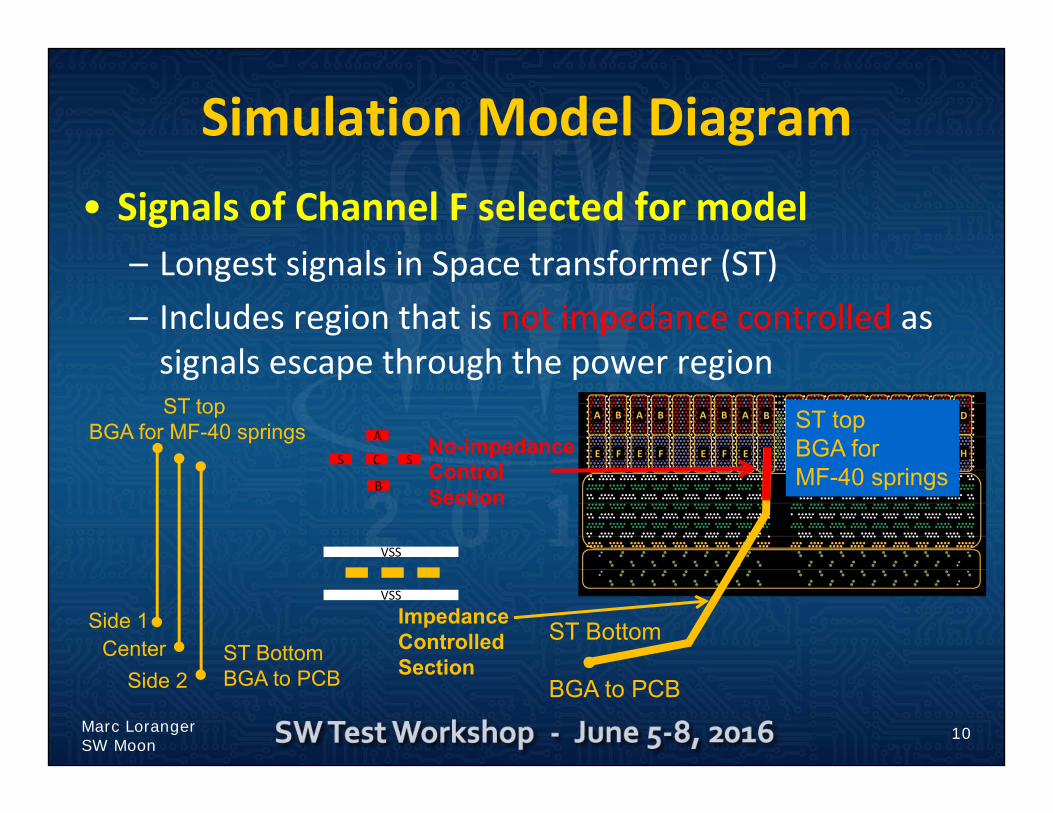
Simulation Model Diagram• Signals of Channel F selected for model
– Longest signals in Space transformer (ST)– Includes region that is not impedance controlled as signals escape through the power region
10Marc Loranger SW Moon
ST Bottom
BGA to PCB
ST top BGA for MF-40 springs
ST top BGA for MF-40 springs
ST BottomBGA to PCB
CenterSide 1
Side 2
S C
VSS
VSS
S
B
A No-impedanceControlSection
ImpedanceControlledSection
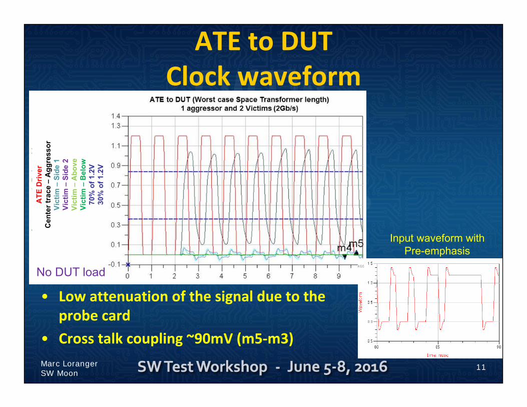
ATE to DUTClock waveform
• Low attenuation of the signal due to the probe card
• Cross talk coupling ~90mV (m5‐m3)
11
Input waveform with Pre-emphasis
Marc Loranger SW Moon
No DUT load
ATE
Driv
er
Cen
ter t
race
–A
ggre
ssor
Vict
im –
Side
1Vi
ctim
–Si
de 2
Vict
im –
Abo
veVi
ctim
–B
elow
70%
of 1
.2V
30%
of 1
.2V
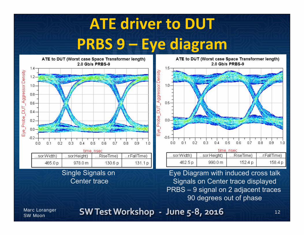
ATE driver to DUT PRBS 9 – Eye diagram
12
Single Signals on Center trace
Eye Diagram with induced cross talkSignals on Center trace displayed
PRBS – 9 signal on 2 adjacent traces 90 degrees out of phase
Marc Loranger SW Moon
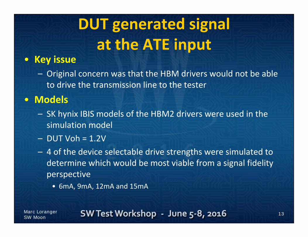
DUT generated signal at the ATE input
• Key issue– Original concern was that the HBM drivers would not be able to drive the transmission line to the tester
• Models– SK hynix IBIS models of the HBM2 drivers were used in the simulation model
– DUT Voh = 1.2V– 4 of the device selectable drive strengths were simulated to determine which would be most viable from a signal fidelity perspective• 6mA, 9mA, 12mA and 15mA
13Marc Loranger SW Moon
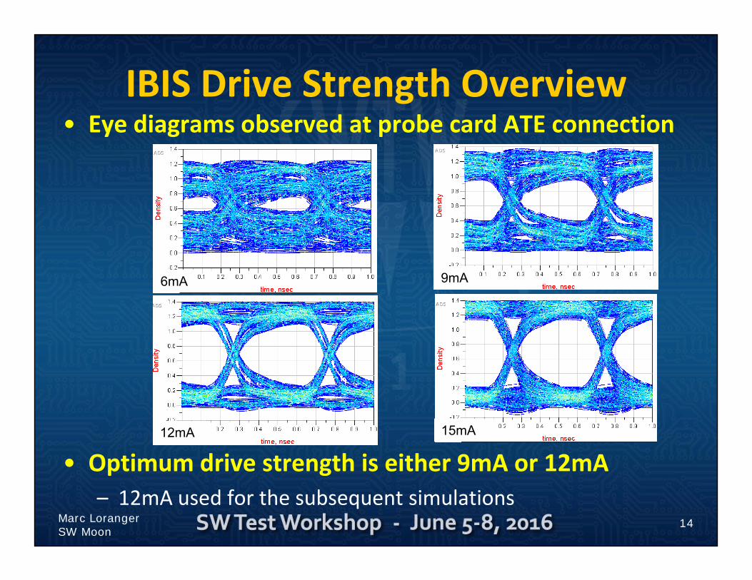
IBIS Drive Strength Overview• Eye diagrams observed at probe card ATE connection
• Optimum drive strength is either 9mA or 12mA– 12mA used for the subsequent simulations
14
6mA 9mA
12mA 15mA
Marc Loranger SW Moon
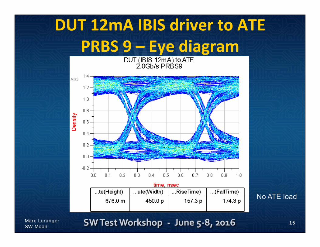
DUT 12mA IBIS driver to ATEPRBS 9 – Eye diagram
15
No ATE load
Marc Loranger SW Moon
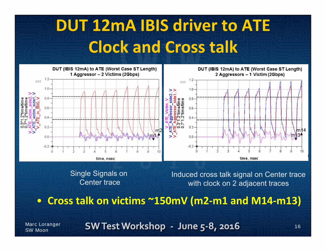
DUT 12mA IBIS driver to ATEClock and Cross talk
16Marc Loranger SW Moon
Single Signals on Center trace
Induced cross talk signal on Center trace with clock on 2 adjacent traces
• Cross talk on victims ~150mV (m2‐m1 and M14‐m13)
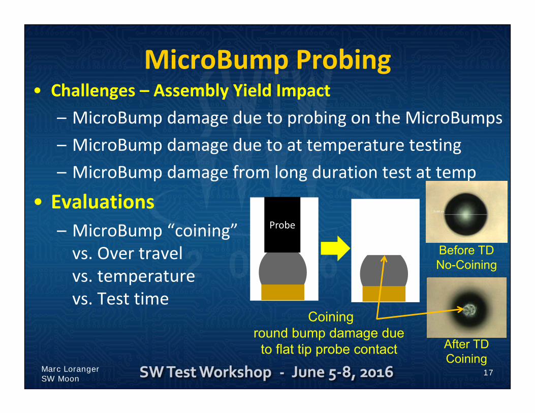
MicroBump Probing• Challenges – Assembly Yield Impact
– MicroBump damage due to probing on the MicroBumps– MicroBump damage due to at temperature testing– MicroBump damage from long duration test at temp
• Evaluations– MicroBump “coining” vs. Over travelvs. temperature vs. Test time
17Marc Loranger SW Moon
Coininground bump damage due to flat tip probe contact
Probe
Before TDNo-Coining
After TDCoining
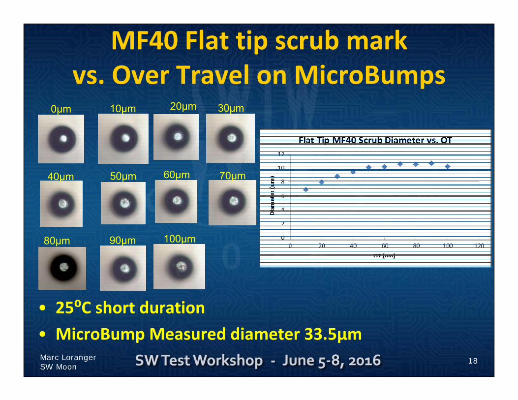
MF40 Flat tip scrub mark vs. Over Travel on MicroBumps
• 25⁰C short duration• MicroBump Measured diameter 33.5µm
18
0µm 10µm 20µm 30µm
40µm 50µm 60µm 70µm
80µm OD
90µm OD
100µm OD
Marc Loranger SW Moon
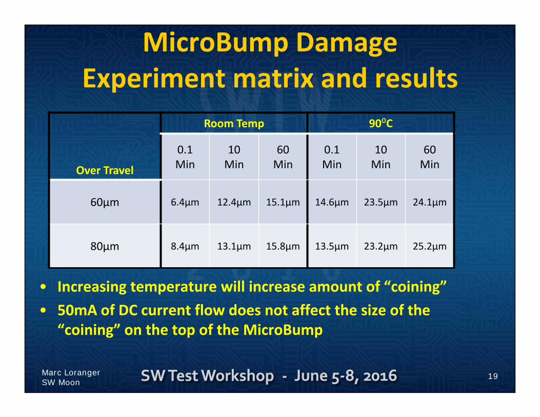
MicroBump Damage Experiment matrix and results
• Increasing temperature will increase amount of “coining”• 50mA of DC current flow does not affect the size of the
“coining” on the top of the MicroBump
19Marc Loranger SW Moon
Over Travel
Room Temp 90⁰C
0.1Min
10Min
60Min
0.1Min
10Min
60Min
60µm 6.4µm 12.4µm 15.1µm 14.6µm 23.5µm 24.1µm
80µm 8.4µm 13.1µm 15.8µm 13.5µm 23.2µm 25.2µm
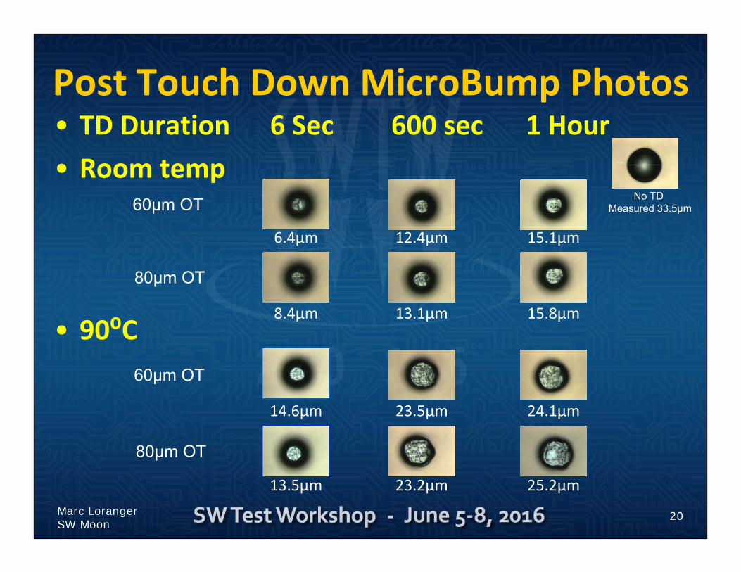
Post Touch Down MicroBump Photos• TD Duration 6 Sec 600 sec 1 Hour• Room temp
• 90⁰C
20Marc Loranger SW Moon
60µm OT
80µm OT
60µm OT
80µm OT
No TD Measured 33.5µm
6.4µm 12.4µm 15.1µm
8.4µm 13.1µm 15.8µm
14.6µm 23.5µm 24.1µm
13.5µm 23.2µm 25.2µm
Direct on MicroBump Probing Summary
• Electrical Test – Signals paths– Simulation models of the DUT and of the Space Transformer show testing can be done at the device specified operating rate of 2Gb/s on the full 8 channels of the HBM Stack
• MicroBump Probing– Using fine pitch FormFactor MF‐40 probes at the 55µm HBM bump pitch shows increasing MicroBump coining when probing at 90⁰C for > 10 min
• Future work– Evaluation of MicroBump probing on singulated stacks
21Marc Loranger SW Moon
We thank the following for providing support to the development of this material
Kelvin ChingClarence GapayUyen NguyenDoug OndricekTodd Swart
22Marc Loranger SW Moon