Embed Size (px)
Citation preview
Ž .Diamond and Related Materials 9 2000 1979]1983
UV Raman characteristics of nanocrystalline diamond filmswith different grain size
Z. SunU, J.R. Shi, B.K. Tay, S.P. LauSchool of Electrical & Electronic Engineering, Nanyang Technological Uni ersity, Singapore 639798, Singapore
Received 14 February 2000; accepted 5 July 2000
Abstract
Ž . Ž .Nanocrystalline diamond films with different size were characterized by ultraviolet UV 244 nm Raman spectroscopy. It wasfound that a diamond peak at 1333 cmy1 was enhanced, while the D and G peak of graphite as well as photoluminescence was
Ž .suppressed, compared with that measured by visible 514.5 nm Raman. With decreasing the particle size from 120 to 28 nm, thediamond peak shifts from 1332.8 to 1329.6 cmy1, the line width of the peak becomes broader, the intensity ratio of diamond andG peak decreases. The down shift and broadening of the diamond peak depending on the particle size by UV Ramanmeasurements are consistent with the phonon confinement model. Q 2000 Published by Elsevier Science S.A.
PACS: 82.80.Ch; 81.10.Bk; 81.15.Gh; 68.55.Jk
Keywords: Diamond film; Raman spectroscopy; Chemical vapor deposition; Grain size
1. Introduction
Ž .Nanocrystalline diamond films NDFs that possesssmooth surfaces are optically transparent, display a lowcoefficient of friction and low electron emission thresh-old voltage. These properties promise a wide range ofapplications in optics, tribology and in field emission
w xdisplay 1,2 . Generally, diamond films are character-ized by Raman spectroscopy in which a visible laserŽ .514.5 nm is used for excitation, and a sharp peak at1333 cmy1 appears in the spectrum. For NDFs, withdecreasing the grain size, the grain surface area andgrain boundary that mainly consists of amorphous sp2
C phases will increase. Raman spectroscopy of NDF,obtained with photons in the visible range, does notappear to provide a good representation of diamondphase in the film. In the Raman spectrum, a broad D
U Corresponding author. Tel.: q65-790-5454; fax: q65-791-2687.Ž .E-mail address: [email protected] Z. Sun .
Ž . y1peak disorder-induced mode at 1350 cm will ap-pear and possibly overlap the diamond peak at 1333cmy1 with increasing sp2 C bonding. The high fre-quency stretch modes of sp2 C atoms are overempha-
U w xsized due to the p]p transition resonance effect 3 ,and the sp2 C network exhibits resonance enhance-ment in the Raman cross-section since the local sp2 Cenergy gap of approximately 2 eV is comparable withthe energy of the incident photons. The sp3 C atoms donot exhibit such a resonance effect because of thehigher local gap of approximately 5.5 eV. Hence theRaman spectra obtained with visible excitation are
2 w xcompletely dominated by the sp C atoms 4 . RamanŽ .scattering in the ultraviolet UV region is promising
3 w xfor vibrational studies of sp -bonded C phase 5 . Ad-vantages of using UV over visible photons include thesuppression of the dominant resonance Raman scatter-ing from sp2 C atoms and the possible increase in theintensity from sp3 C bonding, for which the resonance
w xis expected to be attained 6 . In addition, due to the
0925-9635r00r$ - see front matter Q 2000 Published by Elsevier Science B.V.Ž .PII: S 0 9 2 5 - 9 6 3 5 0 0 0 0 3 4 9 - 6
( )Z. Sun et al. r Diamond and Related Materials 9 2000 1979]19831980
w xhigh concentration of defects in NDFs 7 , the pho-toluminescence effect which has a high intensity back-ground for fine grains of diamond in visible Ramanspectrum will be suppressed. However, the characteri-
Ž .zation of NDFs by UV 244 nm Raman spectroscopy isnot well established. In this paper, the results of UVRaman measurements are compared with those of visi-
Ž .ble 514.5 nm Raman spectra, as well as the phononconfinement model.
2. Experiment details
The NDFs were prepared by a conventional hot-Ž . Ž .filament HF chemical vapor deposition CVD system
Ž .in a CH rH mixture. A polymer, poly phenylcarbyne ,4 2was coated on polished Si substrates for enhancing
w xdiamond nucleation in the initial process 8,9 . Thenthe diamond films were deposited by a two-step method.First, the samples were treated at high CH rH ratio4 2of 10% at a temperature of 6008C for 10 min, thendeposited at a temperature of 6508C with variousCH rH ratios for 4 h. The deposition conditions of4 2NDFs is listed in Table 1. The structures of the NDFsat various CH rH ratios were investigated by X-ray4 2
Ž . Ž .diffraction XRD , visible 514.5 nm and UV RamanŽspectroscopy Renishaw, argon ion laser emitting 10
mW at the 244-nm wavelength was used for the analy-sis, the focus laser power on the samples is less than 1
. y1mW . The diamond Raman peak at 1333 cm withline width of 9.4 cmy1 was calibrated by measuring anatural single crystal diamond. The film morphology
Ž .was measured by an atomic force microscopy AFMŽ .Tapping mode .
3. Results and discussion
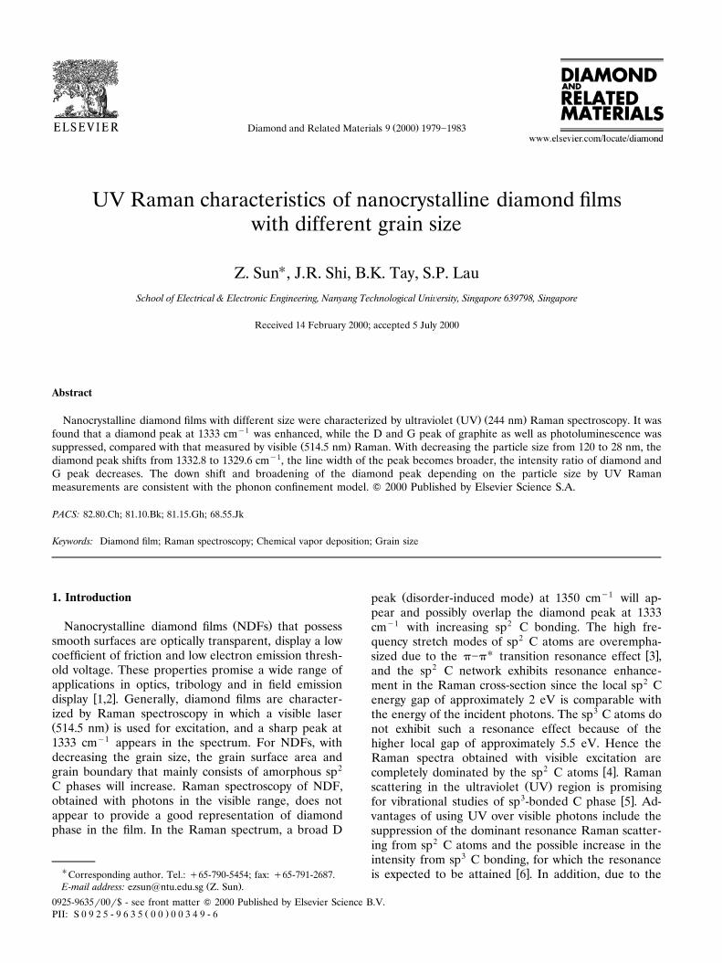
The deposited films are smooth, colorless and trans-parent. XRD analysis of the films indicates onlydiffraction peaks of cubic diamond and silicon. TheŽ .111 peaks of XRD spectra of NDFs grown at various
Ž .CH rH ratios 1%, 2%, 4%, 8% are shown in Fig. 1.4 2Ž .When the CH rH ratio increases, the 111 peak of4 2
XRD spectra of NDF becomes broad, due to decreas-
Table 1NDFs deposition conditions
Step 1 2Ž .H flow rate sccm 100 1002Ž .CH flow rate sccm 10 1]84Ž .Gas pressure kPa 10 10
Ž .Filament temperature 8C 2000 2300Ž .Substrate temperature 8C 600 650
Distance between filament 8 8Ž .and substrate mm
Fig. 1. XRD spectra of the NDFs on polymer coated Si substratesdeposited with different CH rH ratios.4 2
ing crystal size. The estimated grain size of NDFs fromŽ . Žthe line width of the 111 peak using the Scherrer
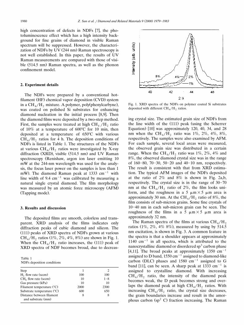
. w xEquation 10 was approximately 120, 40, 34, and 28nm when the CH rH ratio was 1%, 2%, 4%, 8%,4 2respectively. The samples were also examined by AFM.For each sample, several local areas were measured,the observed grain size was distributed in a certainrange. When the CH rH ratio was 1%, 2%, 4% and4 28%, the observed diamond crystal size was in the rangeof 160]80, 70]30, 50]20 and 40]10 nm, respectively.The result is consistent with that from XRD estima-tion. The typical AFM images of the NDFs depositedat the ratio of 2% and 8% is shown in Fig. 2a,b,respectively. The crystal size is in the range of 30]70nm at the CH rH ratio of 2%, the film looks uni-4 2form, and the roughness in a 5 mm=5 mm area isapproximately 30 nm. At the CH rH ratio of 8%, the4 2film consists of sub-micron grains. Some fine crystals of10]40 nm in each sub-micron grain can be seen. Theroughness of the films in a 5 mm=5 mm area isapproximately 32 nm.
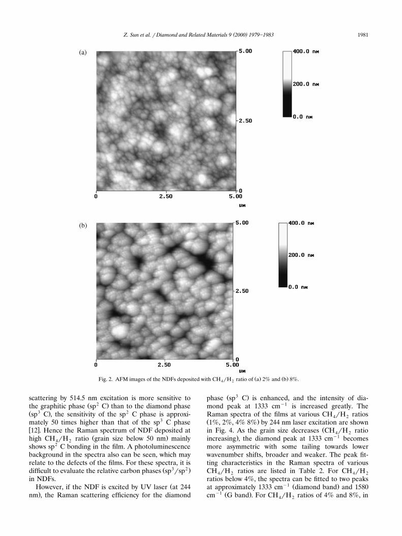
The Raman spectra of the films at various CH rH4 2Ž .ratios 1%, 2%, 4% 8% , measured by using by 514.5
nm excitation, is shown in Fig. 3. A common feature inthe spectra is that a shoulder appears at approximately1140 cmy1 in all spectra, which is attributed to thenanocrystalline diamond or disordered sp3 carbon phasew x y14,11 . The broad peaks at approximately 1350 cmassigned to D band, 1550 cmy1 assigned to diamond-like
Ž . y1carbon DLC phases and 1580 cm assigned to Gw x y1band 11 , can be seen. A sharp peak at 1333 cm is
assigned to crystalline diamond. With increasingCH rH ratio, the intensity of the diamond peak4 2becomes weak, the D peak becomes strong and over-laps the diamond peak at high CH rH ratios. With4 2increasing CH rH ratio, the crystal size decreases,4 2the grain boundaries increase and result in the amor-
Ž 2 .phous carbon sp C fraction increasing. The Raman
( )Z. Sun et al. r Diamond and Related Materials 9 2000 1979]1983 1981
Ž . Ž .Fig. 2. AFM images of the NDFs deposited with CH rH ratio of a 2% and b 8%.4 2
scattering by 514.5 nm excitation is more sensitive toŽ 2 .the graphitic phase sp C than to the diamond phase
Ž 3 . 2sp C , the sensitivity of the sp C phase is approxi-mately 50 times higher than that of the sp3 C phasew x12 . Hence the Raman spectrum of NDF deposited at
Ž .high CH rH ratio grain size below 50 nm mainly4 2shows sp2 C bonding in the film. A photoluminescencebackground in the spectra also can be seen, which mayrelate to the defects of the films. For these spectra, it is
Ž 3 2 .difficult to evaluate the relative carbon phases sp rspin NDFs.
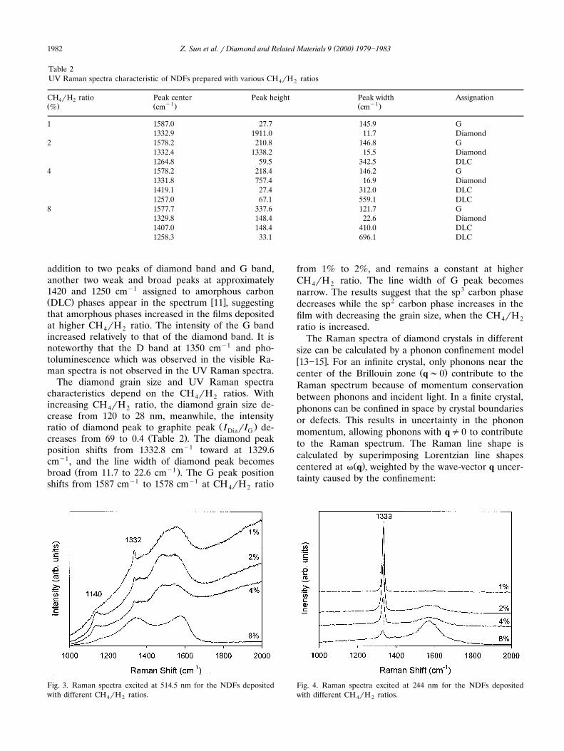
ŽHowever, if the NDF is excited by UV laser at 244.nm , the Raman scattering efficiency for the diamond
Ž 3 .phase sp C is enhanced, and the intensity of dia-mond peak at 1333 cmy1 is increased greatly. TheRaman spectra of the films at various CH rH ratios4 2Ž .1%, 2%, 4% 8% by 244 nm laser excitation are shown
Žin Fig. 4. As the grain size decreases CH rH ratio4 2. y1increasing , the diamond peak at 1333 cm becomes
more asymmetric with some tailing towards lowerwavenumber shifts, broader and weaker. The peak fit-ting characteristics in the Raman spectra of variousCH rH ratios are listed in Table 2. For CH rH4 2 4 2ratios below 4%, the spectra can be fitted to two peaks
y1 Ž .at approximately 1333 cm diamond band and 1580y1 Ž .cm G band . For CH rH ratios of 4% and 8%, in4 2
( )Z. Sun et al. r Diamond and Related Materials 9 2000 1979]19831982
Table 2UV Raman spectra characteristic of NDFs prepared with various CH rH ratios4 2
CH rH ratio Peak center Peak height Peak width Assignation4 2y1 y1Ž . Ž . Ž .% cm cm
1 1587.0 27.7 145.9 G1332.9 1911.0 11.7 Diamond
2 1578.2 210.8 146.8 G1332.4 1338.2 15.5 Diamond1264.8 59.5 342.5 DLC
4 1578.2 218.4 146.2 G1331.8 757.4 16.9 Diamond1419.1 27.4 312.0 DLC1257.0 67.1 559.1 DLC
8 1577.7 337.6 121.7 G1329.8 148.4 22.6 Diamond1407.0 148.4 410.0 DLC1258.3 33.1 696.1 DLC
addition to two peaks of diamond band and G band,another two weak and broad peaks at approximately1420 and 1250 cmy1 assigned to amorphous carbonŽ . w xDLC phases appear in the spectrum 11 , suggestingthat amorphous phases increased in the films depositedat higher CH rH ratio. The intensity of the G band4 2increased relatively to that of the diamond band. It isnoteworthy that the D band at 1350 cmy1 and pho-toluminescence which was observed in the visible Ra-man spectra is not observed in the UV Raman spectra.
The diamond grain size and UV Raman spectracharacteristics depend on the CH rH ratios. With4 2increasing CH rH ratio, the diamond grain size de-4 2crease from 120 to 28 nm, meanwhile, the intensity
Ž .ratio of diamond peak to graphite peak I rI de-Dia GŽ .creases from 69 to 0.4 Table 2 . The diamond peak
position shifts from 1332.8 cmy1 toward at 1329.6cmy1, and the line width of diamond peak becomes
Ž y1 .broad from 11.7 to 22.6 cm . The G peak positionshifts from 1587 cmy1 to 1578 cmy1 at CH rH ratio4 2
Fig. 3. Raman spectra excited at 514.5 nm for the NDFs depositedwith different CH rH ratios.4 2
from 1% to 2%, and remains a constant at higherCH rH ratio. The line width of G peak becomes4 2narrow. The results suggest that the sp3 carbon phasedecreases while the sp2 carbon phase increases in thefilm with decreasing the grain size, when the CH rH4 2ratio is increased.
The Raman spectra of diamond crystals in differentsize can be calculated by a phonon confinement modelw x13]15 . For an infinite crystal, only phonons near the
Ž .center of the Brillouin zone q;0 contribute to theRaman spectrum because of momentum conservationbetween phonons and incident light. In a finite crystal,phonons can be confined in space by crystal boundariesor defects. This results in uncertainty in the phononmomentum, allowing phonons with q/0 to contributeto the Raman spectrum. The Raman line shape iscalculated by superimposing Lorentzian line shapes
Ž .centered at v q , weighted by the wave-vector q uncer-tainty caused by the confinement:
Fig. 4. Raman spectra excited at 244 nm for the NDFs depositedwith different CH rH ratios.4 2
( )Z. Sun et al. r Diamond and Related Materials 9 2000 1979]1983 1983
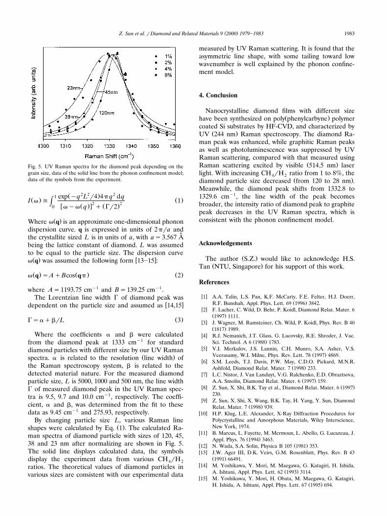
Fig. 5. UV Raman spectra for the diamond peak depending on thegrain size, data of the solid line from the phonon confinement model;data of the symbols from the experiment.
Ž 2 2 . 21 exp yq L r4 4p q dqŽ . Ž .I v ( 1H 2 2w Ž .x Ž .0 vyv q q Gr2
Ž .Where v q is an approximate one-dimensional phonondispersion curve. q is expressed in units of 2pra and
˚the crystallite sized L is in units of a, with as3.567 Abeing the lattice constant of diamond. L was assumedto be equal to the particle size. The dispersion curveŽ . w xv q was assumed the following form 13]15 :
Ž . Ž . Ž .v q sAqBcos qp 2
where As1193.75 cmy1 and Bs139.25 cmy1.The Lorentzian line width G of diamond peak was
w xdependent on the particle size and assumed as 14,15
Ž .GsaqbrL 3
Where the coefficients a and b were calculatedfrom the diamond peak at 1333 cmy1 for standarddiamond particles with different size by our UV Raman
Ž .spectra. a is related to the resolution line width ofthe Raman spectroscopy system, b is related to thedetected material nature. For the measured diamondparticle size, L is 5000, 1000 and 500 nm, the line widthG of measured diamond peak in the UV Raman spec-tra is 9.5, 9.7 and 10.0 cmy1, respectively. The coeffi-cient, a and b, was determined from the fit to thesedata as 9.45 cmy1 and 275.93, respectively.
By changing particle size L, various Raman lineŽ .shapes were calculated by Eq. 1 . The calculated Ra-
man spectra of diamond particle with sizes of 120, 45,38 and 23 nm after normalizing are shown in Fig. 5.The solid line displays calculated data, the symbolsdisplay the experiment data from various CH rH4 2ratios. The theoretical values of diamond particles invarious sizes are consistent with our experimental data
measured by UV Raman scattering. It is found that theasymmetric line shape, with some tailing toward lowwavenumber is well explained by the phonon confine-ment model.
4. Conclusion
Nanocrystalline diamond films with different sizeŽ .have been synthesized on poly phenylcarbyne polymer
coated Si substrates by HF-CVD, and characterized byŽ .UV 244 nm Raman spectroscopy. The diamond Ra-
man peak was enhanced, while graphitic Raman peaksas well as photoluminescence was suppressed by UVRaman scattering, compared with that measured using
Ž .Raman scattering excited by visible 514.5 nm laserlight. With increasing CH rH ratio from 1 to 8%, the4 2
Ž .diamond particle size decreased from 120 to 28 nm .Meanwhile, the diamond peak shifts from 1332.8 to1329.6 cmy1, the line width of the peak becomesbroader, the intensity ratio of diamond peak to graphitepeak decreases in the UV Raman spectra, which isconsistent with the phonon confinement model.
Acknowledgements
Ž .The author S.Z. would like to acknowledge H.S.Ž .Tan NTU, Singapore for his support of this work.
References
w x1 A.A. Talin, L.S. Pan, K.F. McCarty, F.E. Felter, H.J. Doerr,Ž .R.F. Bunshah, Appl. Phys. Lett. 69 1996 3842.
w x2 F. Lacher, C. Wild, D. Behr, P. Koidl, Diamond Relat. Mater. 6Ž .1997 1111.
w x3 J. Wagner, M. Ramsteiner, Ch. Wild, P. Koidl, Phys. Rev. B 40Ž .1817 1989.
w x4 R.J. Nemanich, J.T. Glass, G. Lucovsky, R.E. Shroder, J. Vac.Ž .Sci. Technol. A 6 1988 1783.
w x5 V.I. Merkulov, J.S. Lannin, C.H. Munro, S.A. Asher, V.S.Ž .Veerasamy, W.I. Milne, Phys. Rev. Lett. 78 1997 4869.
w x6 S.M. Leeds, T.J. Davis, P.W. May, C.D.O. Pickard, M.N.R.Ž .Ashfold, Diamond Relat. Mater. 7 1998 233.
w x7 L.C. Nistor, J. Van Landuyt, V.G. Ralchenko, E.D. Obraztsova,Ž .A.A. Smolin, Diamond Relat. Mater. 6 1997 159.
w x Ž .8 Z. Sun, X. Shi, B.K. Tay et al., Diamond Relat. Mater. 6 1997230.
w x9 Z. Sun, X. Shi, X. Wang, B.K. Tay, H. Yang, Y. Sun, DiamondŽ .Relat. Mater. 7 1998 939.
w x10 H.P. Klug, L.E. Alexander, X-Ray Diffraction Procedures forPolycrystalline and Amorphous Materials, Wiley Interscience,New York, 1974.
w x11 B. Marcus, L. Fayette, M. Mermoux, L. Abello, G. Lucazeau, J.Ž .Appl. Phys. 76 1994 3463.
w x Ž .12 N. Wada, S.A. Solin, Physica B 105 1981 353.w x13 J.W. Ager III, D.K. Veirs, G.M. Rosenblatt, Phys. Rev. B 43
Ž .1991 66491.w x14 M. Yoshikawa, Y. Mori, M. Maegawa, G. Katagiri, H. Ishida,
Ž .A. Ishtani, Appl. Phys. Lett. 62 1993 3114.w x15 M. Yoshikawa, Y. Mori, H. Obata, M. Maegawa, G. Katagiri,
Ž .H. Ishida, A. Ishtani, Appl. Phys. Lett. 67 1995 694.