Embed Size (px)
Citation preview
Using the TASKING PinMapper for AURIX
MA160-870 (v1.0) February 12, 2016

Copyright © 2016 Altium BV.
All rights reserved.You are permitted to print this document provided that (1) the use of such is for personal use onlyand will not be copied or posted on any network computer or broadcast in any media, and (2) no modifications of thedocument is made. Unauthorized duplication, in whole or part, of this document by any means, mechanical or electronic,including translation into another language, except for brief excerpts in published reviews, is prohibited without theexpress written permission of Altium BV. Unauthorized duplication of this work may also be prohibited by local statute.Violators may be subject to both criminal and civil penalties, including fines and/or imprisonment. Altium, TASKING,and their respective logos are trademarks or registered trademarks of Altium Limited or its subsidiaries. All otherregistered or unregistered trademarks referenced herein are the property of their respective owners and no trademarkrights to the same are claimed.
Table of Contents1. Introduction .................................................................................................................. 1
1.1. Port Pin ............................................................................................................. 11.2. Peripheral .......................................................................................................... 11.3. Connection ........................................................................................................ 11.4. Package ............................................................................................................ 2
2. Getting Started with the TASKING Pin Mapper ..................................................................... 32.1. Adding a Pin Mapper Document to an Existing Project ................................................ 32.2. TASKING Pin Mapper Perspective .......................................................................... 4
2.2.1. TASKING Pin Mapper Editor View ................................................................ 52.2.2. Package View .......................................................................................... 92.2.3. Pin Conflicts View .................................................................................... 12
2.3. Configuring the Pins ........................................................................................... 132.4. Solving Pin Conflicts ........................................................................................... 142.5. Generating and Using the Source Code ................................................................. 162.6. Generate CSV File ............................................................................................. 172.7. Launch Altium Designer ...................................................................................... 182.8. Pin Mapper Preferences ...................................................................................... 182.9. Errors and Warnings ........................................................................................... 18
iii

iv
Using the TASKING Pin Mapper for AURIX
Chapter 1. IntroductionNowadays many microcontrollers are equipped with a large number of on-chip peripheral modules.Thesemicrocontrollers are made available in surface mount packages with various numbers of physical pins.The number of pins usually does not allow all peripheral modules to be used simultaneously. Hardwareregisters on the microcontroller allow for configurable assignment of peripheral module signals to physicalpins. This means that you have to select the proper device for your application and properly initializehardware registers from software.The purpose of the TASKING Pin Mapper is to assist you in performingthose tasks.
1.1. Port Pin
The basic entity of the TASKING Pin Mapper is the port pin. Port pins are physical pins of the chip. A portpin name typically consists of a port identifier and, if the port identifier is shared by multiple pins, asequential pin number, for example TMS, AN4 or P10_2. A port pin name is not package specific. Eachpackage has its own specific assignment of port pin names to package pin numbers.
The basic configuration item of a port pin is its function (which in most cases is determined by the signalassigned to it). Some ports have dedicated functions, mostly related to power supply or chip infrastructure.Other ports have configurable functionality (ultimately defined by run-time register settings).The requiredfunction is application specific.
A port function definition consists of a symbolic name, a direction and a description. The TASKING PinMapper distinguishes between input functions and output functions. Functions are listed by their symbolicnames (which are mostly signal names, for example ASCLK3).
Port pins can have a number of other chip specific properties. Such properties can be fixed (for examplethe type of pad the port is connected to) or configurable (for example the pad state). Port pins are visiblein the Package view.You can assign a user-defined symbol name to the port pin and you can make thesymbol names visible in the Package view.You can use filters in pin selection views or you can useproperty values as background color codes in the Package view.You can change the configurable propertyvalues.
1.2. Peripheral
AURIX devices, such as the TC27xC, have support for several on-chip peripherals, such as serialcontrollers, timer units, and analog-to-digital converters.
1.3. Connection
The TASKING Pin Mapper allows you to define connections between modules, where a module is eithera port pin or a peripheral.
You can connect port pin modules to peripheral modules by selecting the pin's Direction and its Chipinput function or its Chip output function. The peripheral module side of a connection is referred to as avirtual pin. Some peripheral modules can also be connected to other peripheral modules. Such a connection
1
is made between two virtual pins. Virtual pins are internal to the chip and are not visible in the Packageview. However, virtual pin conflicts are reported in the Pin Conflicts view, for example when you try toconnect a GTM virtual output pin to a physical port pin and at the same time to a virtual input pin of anADC peripheral module.
If you have defined a connection (either valid or invalid) the "follow the connection" button ( ) becomesavailable and you can navigate from one side of the connection to the other side. This applies to virtualpins as well as physical pins. Virtual pins usually do not have a configurable direction. They are eitherInput or Output (and some virtual pins are bidirectional).
See Section 2.3, Configuring the Pins for a step-by-step example.
1.4. Package
When you create a new pin mapper document, as explained in Section 2.1, Adding a Pin Mapper Documentto an Existing Project, you first select a processor (family), for example TC27XC, and a package, forexample BGA292. This selection defines the package pin numbers and the linking of package pins toport pins. It is possible that a port pin is linked to a single package pin multiple times by means of portpin aliases, for example AN39 and P40_9.
For QFP (Quad Flat Package) type packages the pin number consists of the package identifier and asequential pin number. For BGA (Ball Grid Array) type packages the pin number consists of the packageidentifier and a matrix cell number.
2
Using the TASKING Pin Mapper for AURIX
Chapter 2. Getting Started with the TASKINGPin MapperThe TASKING Pin Mapper is the graphical interface to configure the pins and modules in a package.
2.1. Adding a Pin Mapper Document to an Existing Project
To configure the pins and modules of a package you need to create a project and add a Pin Mapperdocument.
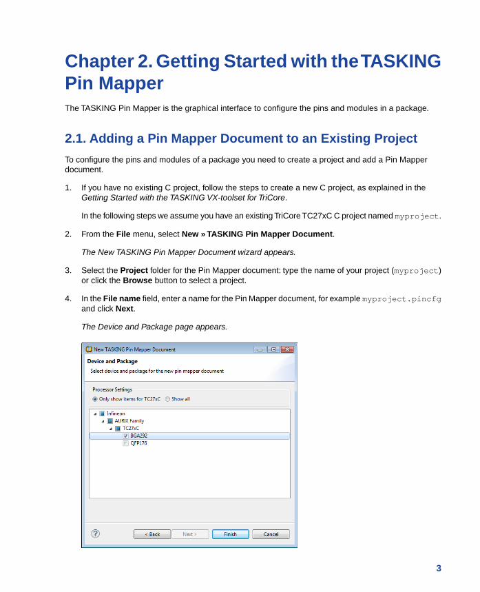
1. If you have no existing C project, follow the steps to create a new C project, as explained in theGetting Started with the TASKING VX-toolset for TriCore.
In the following steps we assume you have an existing TriCore TC27xC C project named myproject.
2. From the File menu, select New » TASKING Pin Mapper Document.
The New TASKING Pin Mapper Document wizard appears.
3. Select the Project folder for the Pin Mapper document: type the name of your project (myproject)or click the Browse button to select a project.
4. In the File name field, enter a name for the Pin Mapper document, for example myproject.pincfgand click Next.
The Device and Package page appears.
3
5. Select the processor, for example TC27xC, and package, for example BGA292, for which you wantto make a pin configuration and click Finish.
A pin configuration file with extension .pincfg is added to the existing project. Because the TASKINGC/C++ perspective is still active, Eclipse asks to open the TASKING Pin Mapper perspective.
6. Optionally, enable the option Remember my decision and click Yes.
The TASKING Pin Mapper perspective is opened.
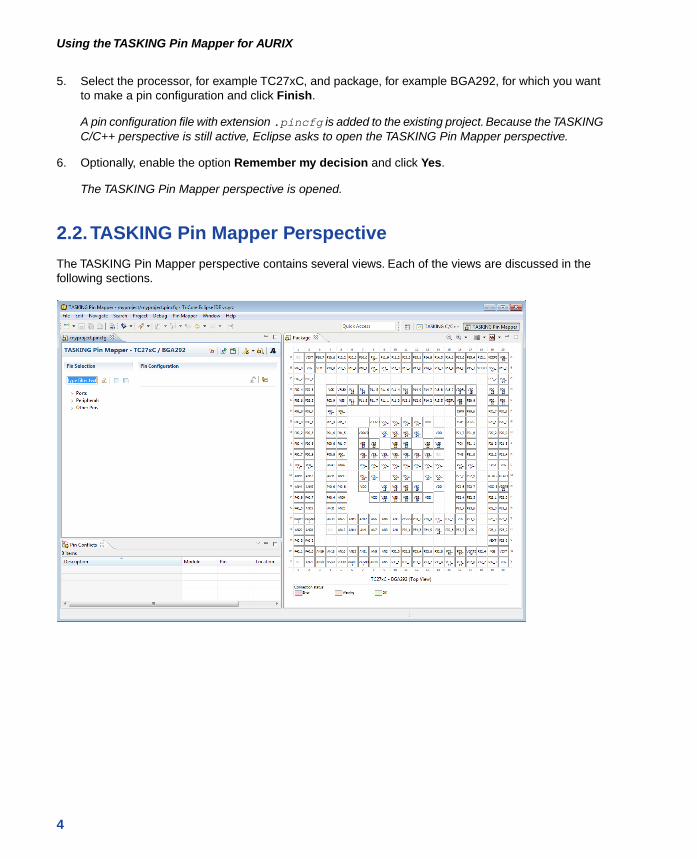
2.2.TASKING Pin Mapper Perspective
The TASKING Pin Mapper perspective contains several views. Each of the views are discussed in thefollowing sections.
4
Using the TASKING Pin Mapper for AURIX
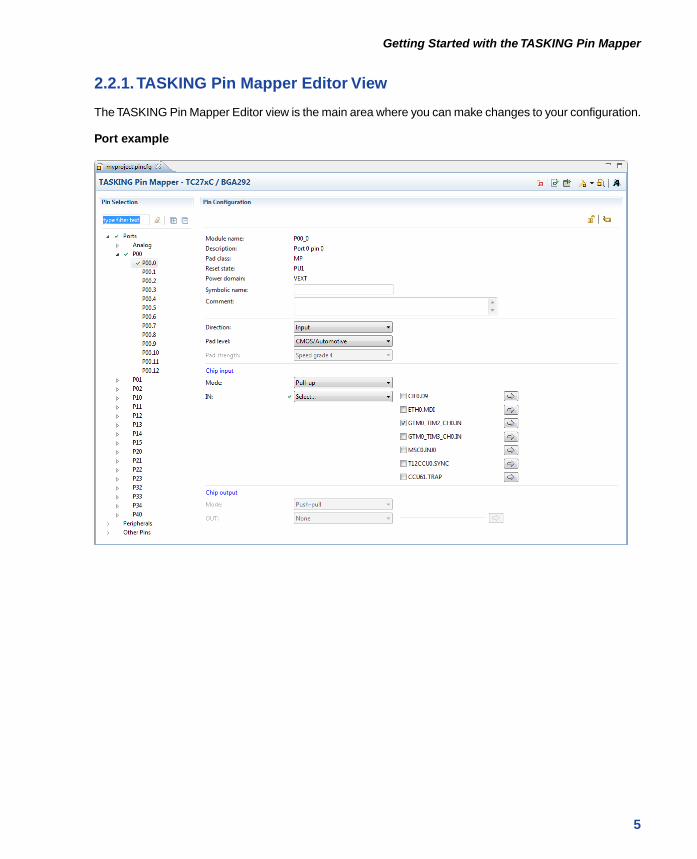
2.2.1.TASKING Pin Mapper Editor View
The TASKING Pin Mapper Editor view is the main area where you can make changes to your configuration.
Port example
5
Getting Started with the TASKING Pin Mapper
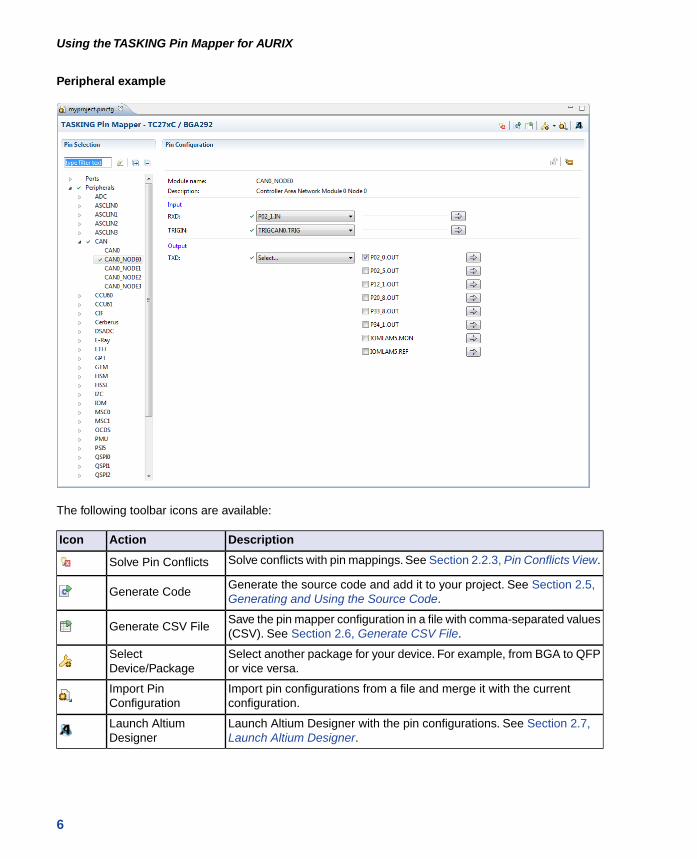
Peripheral example
The following toolbar icons are available:
DescriptionActionIcon
Solve conflicts with pin mappings. See Section 2.2.3, Pin Conflicts View.Solve Pin Conflicts
Generate the source code and add it to your project. See Section 2.5,Generating and Using the Source Code.
Generate Code
Save the pin mapper configuration in a file with comma-separated values(CSV). See Section 2.6, Generate CSV File.
Generate CSV File
Select another package for your device. For example, from BGA to QFPor vice versa.
SelectDevice/Package
Import pin configurations from a file and merge it with the currentconfiguration.
Import PinConfiguration
Launch Altium Designer with the pin configurations. See Section 2.7,Launch Altium Designer.
Launch AltiumDesigner
6
Using the TASKING Pin Mapper for AURIX
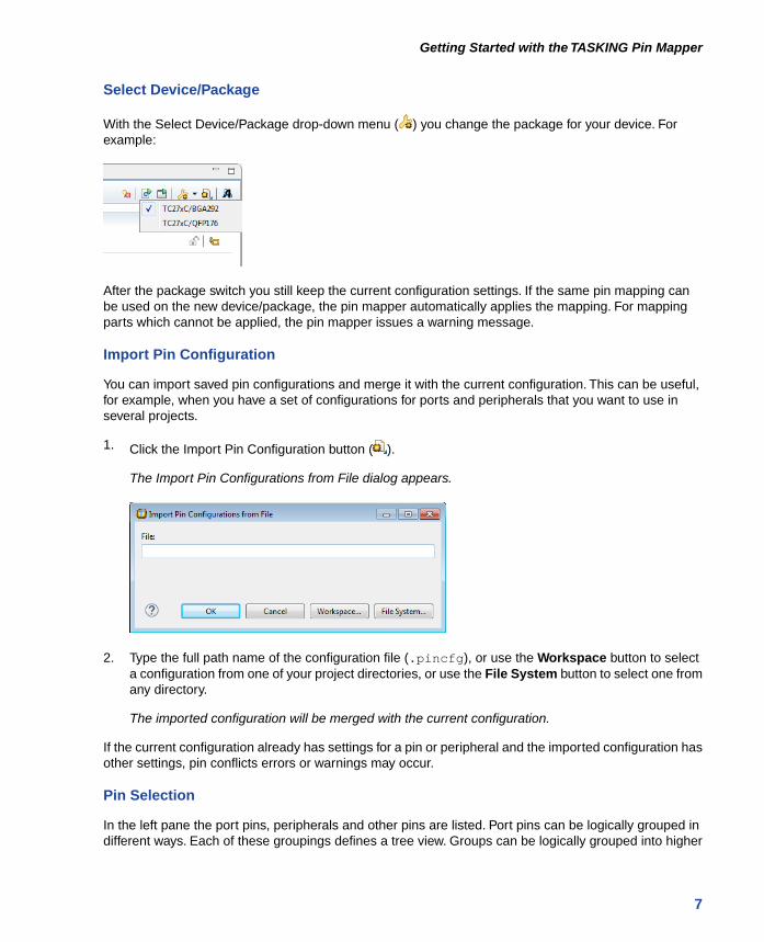
Select Device/Package
With the Select Device/Package drop-down menu ( ) you change the package for your device. Forexample:
After the package switch you still keep the current configuration settings. If the same pin mapping canbe used on the new device/package, the pin mapper automatically applies the mapping. For mappingparts which cannot be applied, the pin mapper issues a warning message.
Import Pin Configuration
You can import saved pin configurations and merge it with the current configuration. This can be useful,for example, when you have a set of configurations for ports and peripherals that you want to use inseveral projects.
1. Click the Import Pin Configuration button ( ).
The Import Pin Configurations from File dialog appears.
2. Type the full path name of the configuration file (.pincfg), or use the Workspace button to selecta configuration from one of your project directories, or use the File System button to select one fromany directory.
The imported configuration will be merged with the current configuration.
If the current configuration already has settings for a pin or peripheral and the imported configuration hasother settings, pin conflicts errors or warnings may occur.
Pin Selection
In the left pane the port pins, peripherals and other pins are listed. Port pins can be logically grouped indifferent ways. Each of these groupings defines a tree view. Groups can be logically grouped into higher
7
Getting Started with the TASKING Pin Mapper
level groups as long as the overall structure can be represented as a mathematical tree. The leafs of thetree are references to port pins, peripherals or peripheral sub-modules.
The tree structure of the grouping allows you to expand and collapse the view.
In the type filter text edit field, you can add a port pin selection filter in order to reduce the numberof visible port pins. The filter is case insensitive. For example, type an to only show pins that have "an"in their name. Wildcards are allowed.
Pin Configuration
When you click on a port or module in the left pane, the configuration appears in the right pane. Thefollowing information can be present:
• Module name - The name of the selected module or port pin.
• Alias - An alias for the module name.
• Description - The description of the selected module or port pin.
• Pad class - The assignment of a port pin to one of the pad classes.
• Reset state - The state of the pin after reset. For example, PU (Pull-up) or PD (Pull-down).
• Power domain - The power domain the pin uses.
• Symbolic name - You can assign a user-defined symbol name to the port pin.You can make thesymbol names visible in the Package view.
• Comment - Any user comments you can add here.
• Pin function - You can configure some pins as digital or analog.
• Direction - You can specify if a pin must be configured as an input pin or an output pin.
• Pad level - Here you can select CMOS/Automotive or TTL.
• Pad strength - For an output pin you can specify the Speed grade.
• Mode - The chip input or output mode. For chip input this can be Pull-up, Pull-down or Tri-state. Forchip output this can be Push-pull or Open drain.
• Other properties allow you to make a pin connection. See Section 2.3, Configuring the Pins for moreinformation.
When you make a selection a '*' can appear in front of other selectable pin names. When you select apin name with a '*', this results in an error.
Lock/Unlock
When you want to be certain that the port settings cannot be changed anymore, you can click the button to lock the current settings.You can always click the button to unlock the settings again.
8
Using the TASKING Pin Mapper for AURIX
Tags
You can assign a tag name to a connection. When you click the (Edit tags) button, you can edit the
tag field to the right of the (Follow connection) button.You can use it the way you want. For example,to tag connections of the same type.
Undo/Redo
You can undo (Ctrl+Z) or redo (Ctrl+Y) one or more actions.
Back/Forward
With the (Back) and (Forward) buttons you can navigate to a previously opened pin configuration.
Save
From the File menu, select Save (Ctrl+S) or click to save the configuration.
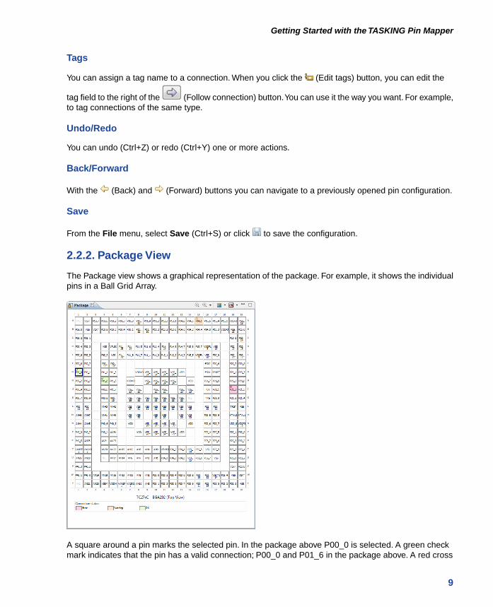
2.2.2. Package View
The Package view shows a graphical representation of the package. For example, it shows the individualpins in a Ball Grid Array.
A square around a pin marks the selected pin. In the package above P00_0 is selected. A green checkmark indicates that the pin has a valid connection; P00_0 and P01_6 in the package above. A red cross
9
Getting Started with the TASKING Pin Mapper
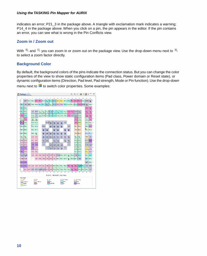
indicates an error; P21_3 in the package above. A triangle with exclamation mark indicates a warning;P14_4 in the package above. When you click on a pin, the pin appears in the editor. If the pin containsan error, you can see what is wrong in the Pin Conflicts view.
Zoom in / Zoom out
With and you can zoom in or zoom out on the package view. Use the drop-down menu next to to select a zoom factor directly.
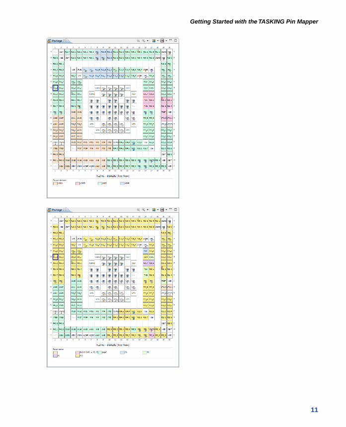
Background Color
By default, the background colors of the pins indicate the connection status. But you can change the colorproperties of the view to show static configuration items (Pad class, Power domain or Reset state), ordynamic configuration items (Direction, Pad level, Pad strength, Mode or Pin function). Use the drop-down
menu next to to switch color properties. Some examples:
10
Using the TASKING Pin Mapper for AURIX
11
Getting Started with the TASKING Pin Mapper
Labels
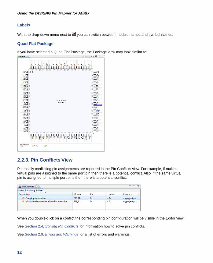
With the drop-down menu next to you can switch between module names and symbol names.
Quad Flat Package
If you have selected a Quad Flat Package, the Package view may look similar to:
2.2.3. Pin Conflicts View
Potentially conflicting pin assignments are reported in the Pin Conflicts view. For example, if multiplevirtual pins are assigned to the same port pin then there is a potential conflict. Also, if the same virtualpin is assigned to multiple port pins then there is a potential conflict.
When you double-click on a conflict the corresponding pin configuration will be visible in the Editor view.
See Section 2.4, Solving Pin Conflicts for information how to solve pin conflicts.
See Section 2.9, Errors and Warnings for a list of errors and warnings.
12
Using the TASKING Pin Mapper for AURIX
2.3. Configuring the Pins
Basically you can connect pins in two different ways. The first way is to select a port pin and then assigna peripheral virtual pin (function) to it. The second way is to select a peripheral virtual pin (function) andthen assign a port pin to it.
You can choose between input or output mode. If an application is going to use a port pin in both directionsthen you should select the initial run-time direction of the port.This is necessary because the pin mapperwill generate port pin initialization code and needs to know whether to configure for input or for output.
To connect pins from the port pin side
1. In the Project Explorer view double-click on a configuration file (myproject.pincfg) to view itscontents.
2. In the Pin selection pane, select a port pin. For example, Ports » P00 » P00_0.
3. In the Pin configuration pane select the Direction: Input or Output. In this example we select Input.
4. Select the pin Mode.
5. Connect the input pin to a peripheral virtual pin:
• From the IN drop-down box choose GPIO or Select...
With Select... a virtual pin appears, or with a 1-to-N connection (one source, many destinations)a list of virtual pins appears.
• Select one (or more) pins.
A green check mark appears if the connection is successful.
6. (Optional) When you want to prevent that these settings can be changed, click to lock the settings.
A little lock appears next to the port pin.
7. From the File menu, select Save (Ctrl+S) or click to save the configuration.
When you click you follow the connection from source to destination or vice versa.The correspondingselection is shown in a light blue color.
To connect pins from the peripheral side
1. In the Project Explorer view double-click on a configuration file (myproject.pincfg) to view itscontents.
2. In the Pin selection pane, select a module. For example, Peripherals » ETH » ETH_0.
3. In the Pin configuration pane select the pin you want to assign to the virtual pin.
13
Getting Started with the TASKING Pin Mapper
A green check mark appears if the connection is successful.
4.Click to follow the connection to the port pin side. The corresponding selection is shown in alight blue color.
5. (Optional) When you want to prevent that these settings can be changed, click to lock the settings.
A little lock appears next to the port pin.
6. From the File menu, select Save (Ctrl+S) or click to save the configuration.
2.4. Solving Pin Conflicts
It is your responsibility to solve any pin conflicts. It is important that there are no conflicts when you usethe tools to generate the code.You can solve the conflicts by hand by making other connections, butwhen there are many conflicts or in situations where most port pins are in use, it can be quite cumbersomeand complex to solve conflicts.The Pin Conflicts Solver can automate this process and solve most conflictsfor you.
To solve pin conflicts
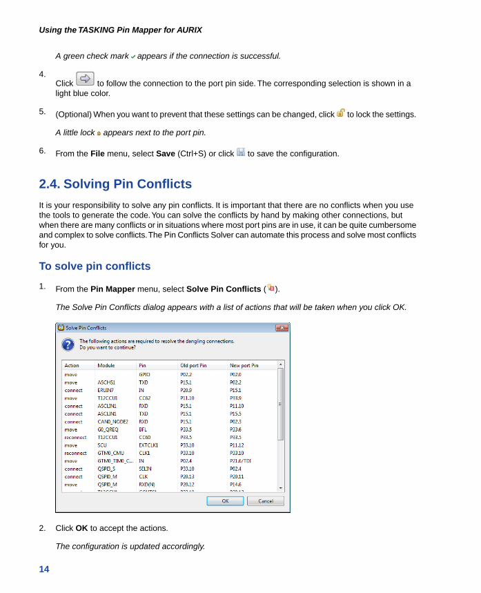
1. From the Pin Mapper menu, select Solve Pin Conflicts ( ).
The Solve Pin Conflicts dialog appears with a list of actions that will be taken when you click OK.
2. Click OK to accept the actions.
The configuration is updated accordingly.
14
Using the TASKING Pin Mapper for AURIX
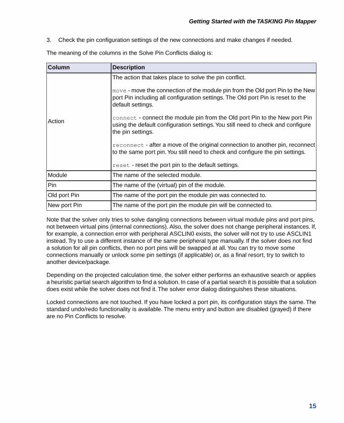
3. Check the pin configuration settings of the new connections and make changes if needed.
The meaning of the columns in the Solve Pin Conflicts dialog is:
DescriptionColumn
The action that takes place to solve the pin conflict.
move - move the connection of the module pin from the Old port Pin to the Newport Pin including all configuration settings. The Old port Pin is reset to thedefault settings.
connect - connect the module pin from the Old port Pin to the New port Pinusing the default configuration settings.You still need to check and configurethe pin settings.
reconnect - after a move of the original connection to another pin, reconnectto the same port pin.You still need to check and configure the pin settings.
reset - reset the port pin to the default settings.
Action
The name of the selected module.Module
The name of the (virtual) pin of the module.Pin
The name of the port pin the module pin was connected to.Old port Pin
The name of the port pin the module pin will be connected to.New port Pin
Note that the solver only tries to solve dangling connections between virtual module pins and port pins,not between virtual pins (internal connections). Also, the solver does not change peripheral instances. If,for example, a connection error with peripheral ASCLIN0 exists, the solver will not try to use ASCLIN1instead. Try to use a different instance of the same peripheral type manually. If the solver does not finda solution for all pin conflicts, then no port pins will be swapped at all.You can try to move someconnections manually or unlock some pin settings (if applicable) or, as a final resort, try to switch toanother device/package.
Depending on the projected calculation time, the solver either performs an exhaustive search or appliesa heuristic partial search algorithm to find a solution. In case of a partial search it is possible that a solutiondoes exist while the solver does not find it. The solver error dialog distinguishes these situations.
Locked connections are not touched. If you have locked a port pin, its configuration stays the same. Thestandard undo/redo functionality is available. The menu entry and button are disabled (grayed) if thereare no Pin Conflicts to resolve.
15
Getting Started with the TASKING Pin Mapper
2.5. Generating and Using the Source Code
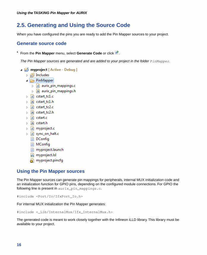
When you have configured the pins you are ready to add the Pin Mapper sources to your project.
Generate source code
• From the Pin Mapper menu, select Generate Code or click .
The Pin Mapper sources are generated and are added to your project in the folder PinMapper.
Using the Pin Mapper sources
The Pin Mapper sources can generate pin mappings for peripherals, internal MUX initialization code andan initialization function for GPIO pins, depending on the configured module connections. For GPIO thefollowing line is present in aurix_pin_mappings.c.
#include <Port/Io/IfxPort_Io.h>
For internal MUX initialization the Pin Mapper generates:
#include <_Lib/InternalMux/Ifx_InternalMux.h>
The generated code is meant to work closely together with the Infineon iLLD library. This library must beavailable to your project.
16
Using the TASKING Pin Mapper for AURIX
You can easily add the Infineon iLLD library to your project by adding a TASKING SoftwarePlatform document and generate the code.
The Software Platform sources are generated in the SoftwarePlatform folder of your project. To usethe generated files, you must add a #include statement into your top-level source file (typically main.c):
#include "swplatform.h"
You can access the Pin Mapper sources from your application. To use the generated files, you must adda #include statement into your top-level source file (typically main.c):
#include "PinMapper/aurix_pin_mappings.h"
You can now use the functions of the Pin Mapper in your sources. For initialization of the GPIO pins orinternal MUX settings, use the initialization functions from the Pin Mapper sources. For initialization ofthe peripherals and other pins use the initialization functions from the iLLD library. For example,
#include "PinMapper/aurix_pin_mappings.h"#include "swplatform.h"
IfxEth *drv;
int main( void ){ /* initialize GPIO */ gpio_init_pins();
/* initialize internal MUX settings */ internal_mux_init();
/* initialize ETH0 */ drv = IfxEth_Phy_Pef7071_ActInit(IFXETH_PHY_PEF7071_1); ...
return 0;}
2.6. Generate CSV File
You can save the pin mapper configuration in a file with comma-separated values (CSV).
• From the Pin Mapper menu, select Generate CSV File ( ).
The CSV file (pincfg_*.csv) is generated in the folder PinMapper of your project.
The following is an example of such a file:
17
Getting Started with the TASKING Pin Mapper
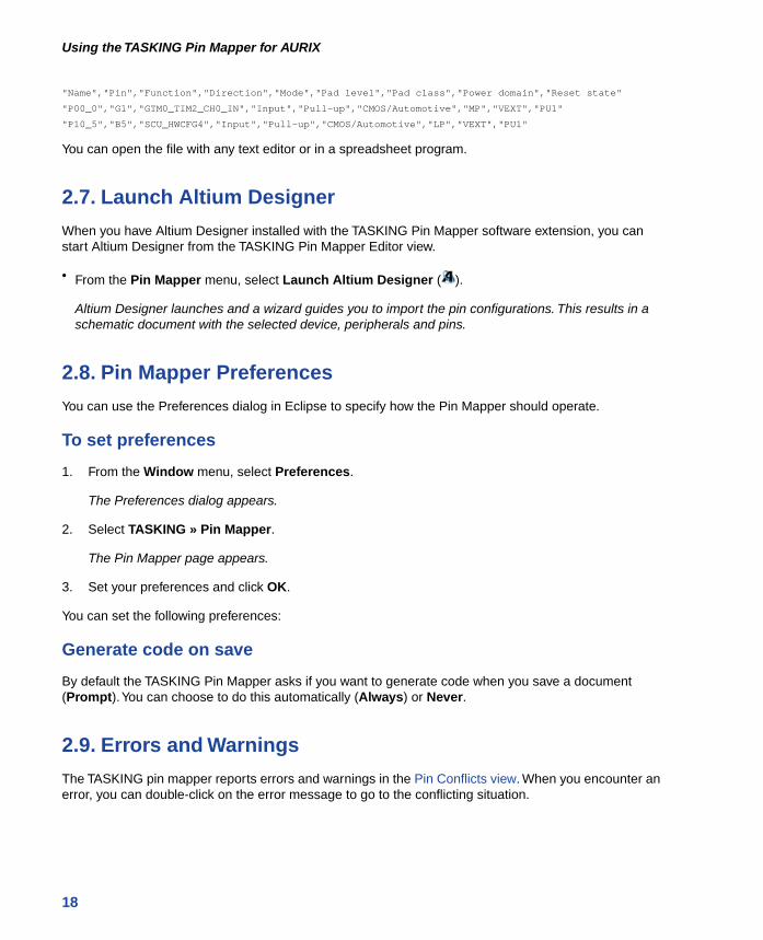
"Name","Pin","Function","Direction","Mode","Pad level","Pad class","Power domain","Reset state"
"P00_0","G1","GTM0_TIM2_CH0_IN","Input","Pull-up","CMOS/Automotive","MP","VEXT","PU1"
"P10_5","B5","SCU_HWCFG4","Input","Pull-up","CMOS/Automotive","LP","VEXT","PU1"
You can open the file with any text editor or in a spreadsheet program.
2.7. Launch Altium Designer
When you have Altium Designer installed with the TASKING Pin Mapper software extension, you canstart Altium Designer from the TASKING Pin Mapper Editor view.
• From the Pin Mapper menu, select Launch Altium Designer ( ).
Altium Designer launches and a wizard guides you to import the pin configurations. This results in aschematic document with the selected device, peripherals and pins.
2.8. Pin Mapper Preferences
You can use the Preferences dialog in Eclipse to specify how the Pin Mapper should operate.
To set preferences
1. From the Window menu, select Preferences.
The Preferences dialog appears.
2. Select TASKING » Pin Mapper.
The Pin Mapper page appears.
3. Set your preferences and click OK.
You can set the following preferences:
Generate code on save
By default the TASKING Pin Mapper asks if you want to generate code when you save a document(Prompt).You can choose to do this automatically (Always) or Never.
2.9. Errors and Warnings
The TASKING pin mapper reports errors and warnings in the Pin Conflicts view. When you encounter anerror, you can double-click on the error message to go to the conflicting situation.
18
Using the TASKING Pin Mapper for AURIX
Error: Dangling connection
A connection consists of two ends; a source and a destination. If the source is connected to a destinationwhile the destination is not connected to the source then the connection is reported to be dangling.Thereare two situations in which this error can appear.
• Situation 1. When dealing with a 1-to-N connection (one source, many destinations), on the right-handside of the drop-down box a list of destinations is shown. Each destination has a check box and youcan make one or more selections. Initially nothing is selected and at that point the error appears.
For example, select Ports » P00 » P00_0 and change the Chip input configuration IN from None toSelect. Several destinations appear, all unselected.The error appears to notify you to make a selection.Once you made a selection, the error disappears.
• Situation 2. When you attempt to connect a source to a destination that already has a connection. Inthis case the source is connected to the destination, while the destination keeps its old connection. Forexample,
1. Select Ports » P00 » P00_0 and change the Direction configuration from Input to Output
2. Change the configuration OUT from None to GPIO.
3. Select Peripherals » GTM » TOUT9 and change the output OUT from None to P00_0.OUT.
The error appears since TOUT9.OUT is now connected to P00_0.OUT, while P00_0.OUT is stillconnected to GPIO.
Error: Incorrect settings for name, expected pins name1 and name2 to beconnected
This error appears when you connect one pin, where multiple pins need to be connected.
For example,
1. Select Ports » P21 » P21_3 and change the Direction configuration from Input to Output.
2. Change the configuration OUT from None to ETH0.MDO3.
The error will disappear when you follow the connection and also connect input MDI from ETH0 toP21_3.IN.
Error: Modules name1 and name2 cannot be used at the same time, sincethey are mutually exclusive
This error appears when you try two use two modules of which only one module can be used at a time.
For example,
1. Select Peripherals » ASCLIN0 » SPI3W0 and change the input RXD(N) from None to P14_1.IN.
19
Getting Started with the TASKING Pin Mapper
2. Select Peripherals » ASCLIN0 » SPI4W0 and change the output TXD from None to P14_1.OUT.
Modules SPI4W0 and SPI3W0 cannot be used at the same time.
Warning: Multiple selections for a 1-to-N connection
This warning appears when you make more than one selection for a 1-to-N connection.
For example, select Ports » P00 » P00_0 and change the Chip input configuration IN from None toSelect. Several destinations appear, all unselected. Now select more than one destination. The warningdisappears if you only select one destination.
20
Using the TASKING Pin Mapper for AURIX
![Triple Mapper™ Triple Mapper ™ - [겜맥] 게임을 더욱 재미있게- · 2012-12-13 · Triple MapperTriple Mapper™ ™는는키보드에서사용되는키값을다른개체로옮기는키보드에서사용되는키값을다른개체로옮기는](https://img.dokumen.tips/doc/110x75/5d2afecc88c993140a8d0fdb/triple-mapper-triple-mapper-.jpg)