Embed Size (px)
Citation preview

University of Groningen
Field effect controlled magnetism and magnetotransport in low dimensionsLiang, Lei
IMPORTANT NOTE: You are advised to consult the publisher's version (publisher's PDF) if you wish to cite fromit. Please check the document version below.
Document VersionPublisher's PDF, also known as Version of record
Publication date:2017
Link to publication in University of Groningen/UMCG research database
Citation for published version (APA):Liang, L. (2017). Field effect controlled magnetism and magnetotransport in low dimensions. [Groningen]:Rijksuniversiteit Groningen.
CopyrightOther than for strictly personal use, it is not permitted to download or to forward/distribute the text or part of it without the consent of theauthor(s) and/or copyright holder(s), unless the work is under an open content license (like Creative Commons).
Take-down policyIf you believe that this document breaches copyright please contact us providing details, and we will remove access to the work immediatelyand investigate your claim.
Downloaded from the University of Groningen/UMCG research database (Pure): http://www.rug.nl/research/portal. For technical reasons thenumber of authors shown on this cover page is limited to 10 maximum.
Download date: 21-07-2019

Dedicated to my families and friends

The work described in this thesis was performed in the research group Device Physics and Complex Materials of the Zernike Institute for Advanced Materials at the University of Groningen, the Netherlands. The thesis proposal was awarded an Ubbo Emmius scholarship funded by the University of Groningen and the research was supported by the European Research Council (consolidator grant no. 648855 Ig-QPD) and Dutch national facility NanoLabNL.
© Lei Liang All rights reserved. Figures, images, illustrations of this publication are original unless further noted. No part may be reproduced, stored in a retrieval system, or transmitted, in any form or by any means, without the prior permission of the author before being published on scientific journals. Zernike Institute PhD thesis series 2017-23 ISSN: 1570-1530 ISBN: 978-94-034-0290-1 (hardcopy version) ISBN: 978-94-034-0289-5 (electronic version) Cover design: Lei Liang Printed by: Gildeprint, Enschede Page number: 264 Print date: November 7, 2017

Field Effect Controlled Magnetism and Magnetotransport in Low Dimensions
Proefschrift
ter verkrijging van de graad van doctor aan de Rijksuniversiteit Groningen
op gezag van de Rector Magnificus prof. dr. E. Sterken
en volgens besluit van het College voor Promoties.
De openbare verdediging zal plaatsvinden op
vrijdag 17 november 2017 om 12.45 uur
door
Lei Liang
geboren op 4 augustus 1987 te Shanxi, China
Promotores Prof. dr. J. T. Ye Prof. dr. T. T. M. Palstra Copromotor Dr. G. R. Blake Beoordelingscommissie Prof. dr. B. Koopmans Prof. dr. A. A. Khajetoorians Prof. dr. M. V. Mostovoy

Table of Contents
Preface .................................................................................................................... 1 Emergent Electrical Transport and Magnetism at Low Dimensionality ................. 2 Motivation and Outline of this Thesis .................................................................... 2 How to read this dissertation .................................................................................. 5
1 Ionic Gating Techniques and Magnetic Ionic Liquids .......................................... 8 1.1 Ionic Gating Technique ........................................................................................... 8
1.1.1 Electric double layer transistor ................................................................. 8 1.1.2 Ionic liquid/solid interfacial structure ..................................................... 11 1.1.3 Transfer curve ......................................................................................... 12 1.1.4 Carrier accumulation dynamic ................................................................ 13 1.1.5 Leak current ............................................................................................ 14 1.1.6 Temperature dependence of the ionic mobility ........................................ 16
1.2 Paramagnetic Ionic Liquids ................................................................................... 19 1.2.1 Synthesis ................................................................................................. 19 1.2.2 Differential scanning calorimetry ............................................................. 21 1.2.3 Thermogravimetric analysis .................................................................... 23 1.2.4 X-ray diffraction measurement ................................................................ 24 1.2.5 X-ray photoelectron spectroscopy ........................................................... 24 1.2.6 Magnetic properties ................................................................................. 25
1.3 Summary ............................................................................................................... 27 1.4 References ............................................................................................................. 28
2 Inducing Ferromagnetism in Platinum by Paramagnetic Ionic Gating ............... 33 2.1 Introduction .......................................................................................................... 32
2.1.1 Electrical control of magnetism ............................................................... 32 2.1.2 Magnetism at molecule/metal interface .................................................. 32
2.2 Concept ................................................................................................................. 33 2.2.1 Two-dimensional ferromagnetism ............................................................ 33 2.2.2 Stoner criterion of band ferromagnetism ................................................. 33 2.2.3 Hall effect family and anomalous Hall effect ........................................... 34
2.3 Experiment ............................................................................................................ 37 2.3.1 Device fabrication and transport measurement ....................................... 37 2.3.2 Paramagnetic ionic liquid ........................................................................ 38 2.3.3 Magnetic property ................................................................................... 39 2.3.4 Paramagnetic ionic gating and temperature dependence of resistance .... 40
2.4 Results and Discussion .......................................................................................... 42 2.4.1 Band structure of the ionic gated Pt ....................................................... 42 2.4.2 Perpendicular magnetic anisotropy ......................................................... 43 2.4.3 Temperature-dependent anomalous Hall effect ....................................... 45 2.4.4 Gate-dependent anomalous Hall effect .................................................... 46 2.4.5 Thickness-dependent anomalous Hall effect ............................................ 47 2.4.6 Strong spin-orbit interaction ................................................................... 48

ii Contents
2.4.7 Crossover between weak localization and weak anti-localization ............. 50 2.4.8 Scaling relationship of AHE in PIL-gated Pt and various other systems. 53 2.4.9 Magnetic phase diagram of PIL gated Pt ................................................ 55
2.5 Supplementary information ................................................................................... 57 2.5.1 Transport properties under negative ionic gate bias ................................ 57 2.5.2 Transport properties of PIL-gated gold thin film .................................... 58 2.5.3 Transport properties of PIL-gated palladium film ................................... 59 2.5.4 Transport properties of Pt thin film doped with Fe impurity ................. 60 2.5.5 Gating cycles with sequential switch between PIL and conventional IL . 61 2.5.6 Optical and atomic force microscopy of Pt film before and after gating . 63
2.6 Summary ............................................................................................................... 64 2.7 References ............................................................................................................. 65
3 Discovery of the Kondo Effect in Molecular Spin Doped Platinum Thin Films .. 71 3.1 Introduction .......................................................................................................... 72
3.1.1 Electron transport of metal at low temperature ...................................... 72 3.1.2 Discovery and interpretation of the Kondo effect .................................... 73
3.2 Concepts ................................................................................................................ 74 3.2.1 Ruderman-Kittel-Kasuya-Yosida interaction .......................................... 74 3.2.2 Quantum dots as artificial magnetic impurities ...................................... 75 3.2.3 Doniach diagram and the interplay between Kondo effect and the RKKY interaction .... 75
3.3 Experiments .......................................................................................................... 76 3.3.1 Sample preparation ................................................................................. 76 3.3.2 Paramagnetic ionic gating ....................................................................... 77
3.4 Results and Discussion .......................................................................................... 78 3.4.1 Thickness dependence of transfer curves ................................................. 78 3.4.2 Two-channel model for calculating in Kondo effect measurement ................ 79 3.4.3 Temperature dependence of Rs for a series of film thicknesses ................ 80 3.4.4 The Kondo length scale and gated ion distribution ................................. 81 3.4.5 Analysis of the Kondo parameters with numerical renormalization group method ... 82 3.4.6 Correlation between the Kondo effect and paramagnetic ionic gating ..... 85 3.4.7 Interpretation of the Kondo state in presence of ferromagnetism ............ 86
3.5 Supplementary information ................................................................................... 86 3.5.1 Possible origins account for the low temperature transport other than Kondo effect .... 86 3.5.2 Field dependence of the low temperature behavior ................................. 88
3.6 Summary ............................................................................................................... 91 3.7 References ............................................................................................................. 92
4 Gate-Controlled Spin-Dependent Magnetoresistance of a Platinum|Paramagnetic Insulator Interface ............................................................................................ 95 4.1 Introduction .......................................................................................................... 96
4.1.1 Spintronics .............................................................................................. 96 4.1.2 Molecular spintronics .............................................................................. 97 4.1.3 Paramagnetic ionic gating induced magnetoresistance ............................ 97
4.2 Concepts ................................................................................................................ 98 4.2.1 A brief history of the magnetoresistance ................................................. 98 4.2.2 Anisotropic magnetoresistance .............................................................. 102 4.2.3 Spin-Hall magnetoresistance .................................................................. 102

Contents iii
4.3 Experiments ........................................................................................................ 104 4.3.1 Sample preparation ............................................................................... 104 4.3.2 Electrical measurement method ............................................................ 105 4.3.3 Paramagnetic ionic gating ..................................................................... 106 4.3.4 Magnetic characterization of the PIL .................................................... 107
4.4 Results and Discussion ........................................................................................ 110 4.4.1 Temperature dependence of longitudinal resistance .............................. 110 4.4.2 Modulation of the resistivities ............................................................... 112 4.4.3 Angle dependence of magnetoresistivity ................................................ 112 4.4.4 Field dependence of magnetoresistivity ................................................. 116 4.4.5 Temperature-dependent in-plane magnetoresistivity ............................. 119 4.4.6 Temperature-dependent out-of-plane magnetoresistivity .......................... 122 4.4.7 Temperature-dependent anomalous Hall effect ..................................... 123 4.4.8 Magnetic phase diagram ........................................................................ 125 4.4.9 Theory of spin-dependent magnetoresistance at Pt/paramagnetic insulator interface . 126
4.5 Supplementary Information ................................................................................. 128 4.5.1 Two-channel model of electrical transport with out-of-plane geometry . 128 4.5.2 Comparison of the in-plane magnetoresistance of PIL gated Pt with other systems ... 130 4.5.3 Finite element modeling of the electrical transport ............................... 132
4.6 Summary ............................................................................................................. 134 4.7 References ........................................................................................................... 135
5 Giant Magnetic Anisotropy in Layered Manganese Intercalated Tantalum Disulfide Thin Flake ........................................................................................ 141 5.1 Introduction ........................................................................................................ 142
5.1.1 Layered materials .................................................................................. 142 5.1.2 Transition metal dichalcogenide ............................................................ 144 5.1.3 Types of magnetic anisotropy ............................................................... 145
5.2 Concepts .............................................................................................................. 147 5.2.1 Magnetocrystalline anisotropy ............................................................... 147 5.2.2 SQUID Magnetometry .......................................................................... 150
5.3 Experiments ........................................................................................................ 151 5.3.1 Crystal growth ...................................................................................... 151 5.3.2 X-ray diffraction .................................................................................... 152 5.3.3 Electron diffraction ............................................................................... 154
5.4 Results and discussion ......................................................................................... 154 5.4.1 Magnetic susceptibility measurement .................................................... 154 5.4.2 Determination of the phase transition temperature from Arrott plot .... 154 5.4.3 Field dependence of magnetization ........................................................ 158 5.4.4 Temperature dependence of magnetization ........................................... 159 5.4.5 Magnetic phase diagram ........................................................................ 160 5.4.6 The appearance of spin-flop phase at low temperature ......................... 161 5.4.7 Spin structures of the Mn1/4TaS2 .......................................................... 162
5.5 Supplementary information ................................................................................. 163 5.5.1 Temperature dependence of magnetization ........................................... 163 5.5.2 Field dependence of magnetization with perpendicular magnetic field .. 164 5.5.3 Field-dependent magnetization as a function of temperature ................ 165

iv Contents
5.6 Summary ............................................................................................................. 166 5.7 References ........................................................................................................... 167
6 Spin-Dependent Magnetotransport in Layered Magnetic Mn1/4TaS2 Thin Film ..... 171 6.1 Introduction ........................................................................................................ 172
6.1.1 Physical properties of TaS2 ................................................................... 172 6.1.2 Magnetism of transitional metal intercalated TaS2 ............................... 173
6.2 Concepts .............................................................................................................. 174 6.2.1 Giant magnetoresistance ....................................................................... 174 6.2.2 Band structure of the intercalated transitional metal dichalcogenide .... 176
6.3 Experiments ........................................................................................................ 177 6.3.1 Mechanical cleavage of atomically thin films ........................................ 177 6.3.2 Device fabrication ................................................................................. 179
6.4 Results and discussion ......................................................................................... 179 6.4.1 Temperature dependence of longitudinal resistance .............................. 179 6.4.2 Field-dependent anisotropic magnetoresistance with perpendicular field .... 181 6.4.3 Temperature-dependent magnetoresistance .................................................. 182 6.4.4 Theory of the spin-dependent magnetoresistance .................................. 185 6.4.5 Angle-dependent magnetoresistance ...................................................... 187
6.5 Supplementary information ................................................................................. 188 6.5.1 Determination of the spin-dependent longitudinal resistance ................ 188 6.5.2 Band structure of the Mn intercalated TaS2 ......................................... 189 6.5.3 Anomalous Hall effect of Mn1/4TaS2 ..................................................... 190
6.6 Summary ............................................................................................................. 191 6.7 References ........................................................................................................... 192
7 A magnetically responsive one-dimensional mesoporous material functionalized with paramagnetic ionic liquid ......................................................................... 195 7.1 Introduction ........................................................................................................ 196
7.1.1 Porous material ..................................................................................... 196 7.1.2 Synthesis of mesoporous material using block-copolymer ...................... 197
7.2 Concepts .............................................................................................................. 197 7.2.1 Phase transition of ionic liquid .............................................................. 197 7.2.2 Synthesis of SiO2-based mesoporous template ....................................... 198
7.3 Experiments ........................................................................................................ 200 7.3.1 Synthesis of SBA-15 mesoporous silica .................................................. 200 7.3.2 Encapsulation of paramagnetic ionic liquid ........................................... 200 7.3.3 Synthesis of SiO2 nanospheres as comparison ........................................ 201 7.3.4 Transmission electron microscopy ......................................................... 202 7.3.5 Raman spectra of PIL and the PIL@SBA-15 ........................................ 202
7.4 Results and discussion ......................................................................................... 204 7.4.1 Magnetic susceptibility measurement .................................................... 204 7.4.2 Magnetization curve of PIL@SBA-15 .................................................... 204 7.4.3 Magnetization curve of the precursors ................................................... 205 7.4.4 Low temperature differential scanning calorimetry ............................... 206 7.4.5 Raman spectrum of PIL@SBA-15 ......................................................... 206 7.4.6 Plausible explanation of one-dimensional ferromagnetism ..................... 207
7.5 Conclusion ........................................................................................................... 208

Contents v
7.6 References ........................................................................................................... 209
A Appendix ......................................................................................................... 211
A.1 Micro-fabrication ................................................................................................. 212 A.1.1 Electron-beam lithography .................................................................... 212 A.1.2 Deep-UV optical lithography ................................................................. 215 A.1.3 Magnetron sputtering ............................................................................ 218 A.1.4 Electron beam evaporation ........................................................................ 220 A.1.5 Exfoliation of layered materials ............................................................. 222
A.2 Transport Measurement ...................................................................................... 223 A.2.1 Lock-in technique .................................................................................. 223 A.2.2 Physical property measurement system ................................................ 226 A.2.3 Cryogen free measurement system ........................................................ 227 A.2.3 Magnetic property measurement system ............................................... 228
Summary .............................................................................................................. 231
Samenvatting ....................................................................................................... 237
Acknowledgement ................................................................................................. 243
Index .................................................................................................................... 249


Submitted to Science Advance: Lei Liang, Qihong Chen, Jianming Lu, Wytse Talsma, Juan Shan, Graeme R. Blake, Thomas T. M. Palstra, Jianting Ye– “Inducing ferromagnetism and Kondo effect in platinum by paramagnetic ionic gating”, 2016 (in review)
Preface
here is plenty of room at the bottom” was a famous
lecture given by physicist Richard Feynman in 1959. He
was fascinated by many interesting phenomena at small
scales and was particularly interested in seeing things small. It
turns out to be a great perspective to the recent tremendous
success of nanoscience. Magnetism, on the other hand, is a
quite early discovery in the human history back to ancient
time, when people noticed that lodestones can attract iron
and made them into compass to show directions. Magnetism
is mainly caused by spinning electrons. This spontaneous
effect influences the behavior of other electrons in an
interacting manner. In low dimensions, how do the electron
transport and magnetism differ from the current
understanding is a question that this thesis will try to answer.
“T

2 Preface
P
Emergent Electrical Transport and Magnetism at Low Dimensionality
Lev Landau unveils the profound essence of phase transitions, which is the change of symmetries. For example, the ferromagnetic ordering is due to the breaking of the time-reversal symmetry. Ferroelectricity, on the other hand, is because of the breaking of the spatial inversion symmetry. In low dimensionality, because of the reduced coordination number of the nearest neighboring atoms, the correlation of the electron wavefunctions differ significantly from the bulk, resulting in a strong perturbation of the band structure. Many exotic physical phenomena may stem from it.
The burgeoning opportunities in spintronics benefit a lot from the growing knowledge of the magnetism at nanoscales. Throughout the evolution history of electronic devices, a deeper understanding of magnetism always accompanies with the development of newer techniques. These include the enormous successes of fabricating nanostructures with high-resolution electron-beam/photo lithography as well as the focused ion beam technologies. The breakthrough of the graphene research revitalizes the study of layered materials and successfully drives the limit of devices down to the two-dimensionality. Besides the aforementioned top-down approach, nanodevices can also be constructed bottom-up ascribing to the self-assembly polymer chemistry. This method has become an important supplement to the physics-oriented methods.
Magnetism originates from spinning electrons and orbital motions. Taming spins would require concerted manner of magnetic field, electric field, crystal structure and temperature. The responses of these parameters vary for different materials, which forms the beauty of the physics.
Motivation and Outline of this Thesis
The main objective of this thesis is to explore and understand the electrical transport and magnetism in low-dimensional systems. Instead of complicated preparation of ultrathin films or heterojunctions, ionic gating provides a unique approach to access two-dimensional systems at channel/ionic liquid interface through fabricating an electric double layer transistor. In addition, the vast interests in layered materials since the experimental discovery of graphene boosts the development of new applications based on two-dimensional materials, including their magnetic properties. The outlines of each chapter of this thesis are addressed as follows.
Chapter 1 first presents a general introduction to the ionic gating technique that is widely used in this thesis. The transfer curve of the ionic-gated field effect transistor as well as the kinetic of the involved electrochemistry will be

Preface 3
P
discussed. Later, comprehensive characterizations of the magnetic ionic liquids will be shown.
Chapter 2 starts to explore the possibility of controlling magnetism with electrical means. Ferromagnetism has been successfully switched ON and OFF in platinum (Pt) thin film transistor by paramagnetic ionic gating. In ON state, anomalous Hall effect is used to characterize the magnetic parameters of ferromagnetic Pt. It shows coercivity as large as 1.5 T and a perpendicular magnetic anisotropy that is potentially important for developing new type of spintronics devices. The modification of surface carrier density is analyzed with respect to the band structure of Pt. Large spin-orbit interaction of Pt and its interaction with the magnetic ions are attributed to the emergence of ferromagnetism. In the longitudinal transport, magnetoresistance changing from negative to positive with increasing temperatures is interpreted as crossover between weak localization and weak anti-localization. Besides, clear thickness dependence is found in this system, which displays not only a decline of the ferromagnetism with the increase of film thicknesses but also a sign reversal of the normal Hall coefficient. In the end, a comprehensive phase diagram is constructed for the paramagnetic ionic gated-Pt thin film system.
Chapter 3 focuses on the influence of local magnetic moments on electrical transport of Pt at low temperature from another point of view that is the Kondo effect. Molecular spins have been proved to be effective dopants in inducing complex transport phenomena at metal surfaces. They form mutual interaction with itinerant conduction electrons in a metal at a high concentration without aggregating, which is difficult to reach with other methods. The Kondo effect is investigated with the numerical renormalization group method, from which the Kondo parameters are derived. Normally, the Kondo correlation will be destructed with the presence of ferromagnetism. There are, however, several exceptions that the Kondo effect and magnetic ordering can be coexisting, which originate from the low-dimensionality. Moreover, our results shed light on understanding the itinerant-localized duality of electron transport.
Chapter 4 is devoted to the investigation of the newly found spin-dependent
magnetoresistance at the metal/paramagnetic insulator interface. Magnetoresistance is the core of data storage, sensors and logic devices. Each breakthrough of discovering new types of magnetoresistance in history will lead to a dramatic progress of electronic devices, such as the anisotropic magnetoresistance in sensors and giant magnetoresistance in high capacity data storages. Both of which, however, require the usage of ferromagnets that cause energy loss due to their stray field. We present the experimental results that support the availability of electrical manipulated magnetoresistance based

4 Preface
P
on interaction between conduction electrons in metal and local magnetic moments from a paramagnetic insulator. By virtue of the ionic gating technique, the magnitude of this interaction is determined by the number of ions at the metal surface and their types, which makes it gate controllable. The physics of this unique transport phenomenon is explained by the recently reported spin-Hall magnetoresistance theory that is spin-dependent. Our results demonstrate the opportunity to electrically control the magnetism in low dimension by gating and pave the way of developing new type of spintronic devices.
Chapter 5 moves to the study of transition metal dichalcogenide (TMD). Ever since the experimental discovery of graphene, many layered materials have been studied in terms of their electrical and photonic properties, particularly the large family of TMDs. However, the magnetic properties of these materials are comparably less studied, mostly because pristine TMDs are diamagnetic, which makes them less interesting. By intercalating magnetic ions into the crystal lattice of TMDs, it is possible to introduce fascinating magnetic properties. In this chapter, we will focus on the magnetic measurement of the layered manganese doped tantalum disulfide (Mn1/4TaS2). This material shows extremely large magnetocrystalline anisotropy, which favors ferromagnetic ordering within the layers and antiferromagnetic ordering between the layers. Temperature and angle dependent magnetization and susceptibility measurement are performed to characterize this material. In the end, a magnetic phase diagram is presented as an overview of these unique properties.
Chapter 6 will continue the study of Mn1/4TaS2 from the electrical transport
point of view. Because of the aforementioned large magnetic anisotropy, the atomic thin film of this material exhibits peculiar magnetoresistance. The transport properties are characterized by angular, temperature and field dependent measurements. The simultaneously detected anomalous Hall effect offers further information about the electron conduction mechanism and influence from the intercalated magnetic ions. A spin-dependent giant magnetoresistance type of mechanism is proposed to explain the observed phenomena.
Chapter 7 presents an application in functionalizing nanoporous material
through encapsulation of magnetic ionic liquid (PIL). Strong magnetic response of diamagnetic nanoporous silica is observed after encapsulating PIL molecules into their nanopores. In addition, the phase transition temperature of the PIL is shifted to higher temperature after encapsulation, which is due to stronger correlation between molecules inside the pores. The experiment

Preface 5
P
demonstrates that the PIL is universal besides gating purpose. Considering the large variety of PILs, more applications are expected to be discovered.
Appendix lists the auxiliary means used in this thesis, including the device
fabrication techniques, the preparation of the low-dimensional materials and the measurement methods.
How to read this thesis
This thesis is written in a way that each chapter is independent from each other. You could jump to any chapter that you find interesting and start reading. On the other hand, we try to build up inter-chapter connection in order to unify all chapters into one thesis. If you would like to know more about the related works, you could refer to the Index of the key words. The content was conceived around the same topic: magnetism in low dimensions. Each chapter comprises of seven sections (maybe less), which are:
1. Introduction,
2. Concepts,
3. Experiments,
4. Results and Discussion,
5. Supplementary information,
6. Summary,
7. References.
Start from Introduction, I first brief the audiences the background of the following research. Then, some relevant basic Concepts that will be used later to analyze the data or be helpful to understand the analysis will be presented. Next, I will move to the Experiments: the detail of device fabrication, material synthesis and measurement method will be mentioned. Afterward, the main dish will be served that is the Results and Discussion. In this thesis, electrical and magnetic measurements are the major means of studying samples' physical properties. For big size (in the order of millimeter) or large amount (in the order of milligram) of samples, direct characterization of the magnetization changes can be realized with magnetometry. However, it is not always possible to achieve especially in the case of interfacial effect that accompany with large background signals. In contrast, confining the electric current in low dimensions is much easier, which allows us to investigate the surface and interface behaviors. In some chapters, I split the secondary results into the Supplementary Information, such as many control experiments that increase the credibility of the explanation to our observation,

6 Preface
P
which avoids the redundancy of including everything in the Results and Discussion section. In the end, we will put the main discovery and claims of this chapter in Summary. The References cited in the main text with numbers in square brackets will be listed in the end of each chapter.

In preparation: Lei Liang, Qihong Chen, Wytse Talsma, Graeme R. Blake, Thomas T. M. Palstra, Jianting Ye– “Paramagnetic ionic liquids: a new type of gating media for electric double layer transistor”
Chapter 1
Ionic Gating Techniques and Magnetic Ionic Liquids
agnetic ionic liquid, as its name implies, is a type of
molten salt that reacts to magnetic field. This magneto-
active functional ionic liquid has attracted growing interests in
the field of catalysis, pharmacy and energy application and
studies from electrical and magnetic transport points of view
have not been reported yet. In this chapter, the
paramagnetic ionic gating technique that is widely used in
the following chapters will be explained. We initialize this
technique in an attempt to achieve electrical manipulation of
magnetism. For this purpose, a family of novel functional ionic
liquids that possess magnetic moments will be introduced,
including the synthesis, characterization of physiochemical
properties and applications.
M

8 Chapter1
1
1.1 Ionic Gating Technique
1.1.1 Electric double layer transistor
Before introducing the ionic gating technique, let us first get known what an electric double layer transistor (EDLT) is. EDLT belongs to a kind of field effect transistor (FET), which is a device that uses an electric field to control the electrical conductivity of a channel (Fig. 1.1).
FET consists of three terminals, which are source, drain, and gate electrodes. They can roughly correspond to the emitter, collector and base of the bipolar junction transistor. The names of the terminals refer to their functions. The gate is used to control the current open and close between the source and the drain. Electric current (IDS) flows from the source (S) towards the drain (D) driven by the applied drain-source voltage (VDS) and is influenced by the gate voltage. In our geometry, the source has the lowest potential and is connected with the gate low (VG-) to the ground, while the drain has the highest potential.
The channel of EDLT is normally made of semiconducting materials, where large ON/OFF ratio can be achieved [1]. However, intrinsically metallic materials can also be gated [2-5]. Moreover, even the seemingly insulating material, such as SrTiO3, can be gated to superconducting [6, 7], demonstrating the universality of ionic gating technique as a powerful to induced exotic electronic state in common materials.
Figure. 1.1 Schematic diagram of electric double layer transistor. The D, S, G denote the drain, source and side gate electrode. VDS, VLG, VSG mean the drain-source voltage, liquid gate voltage and solid gate voltage. The liquid gating is performed by formation of electric double layer at channel surface with applying VLG between the side gate electrode and source electrode. The solid gate is carried out with applying VSG between SiO2/Si substrate and source electrode. The source electrode is connected to the ground.

1.1Ionicgatingtechnique 9
1
Compared to the metal–oxide–semiconductor FET, where the gate electrode is deposited on top of the channel; in EDLT, the gate electrode is placed on the side of the channel with a size at least 102 times larger than the size of the channel. Electrolyte-like gating medium is dropped on top of the wafer to fully cover the channel and at least most of the gate electrode. During gating, a high potential (VG+) is applied to the gate electrode. Similar to the electrochemical capacitor, anions with negative charge are attracted to the gate electrode, while cations with positive charge are driven to the surface of the channel. Because of the aspect ratio > 102, the density of ions at the surface of the channel is much larger than the gate electrode. This will allow an effective control of the induced carrier density beneath.
The first reported EDLT is based on ZnO, using polymer electrolyte KClO4/polyethylene oxide (PEO) (molecular weight ≈ 1000) as the gating medium [8]. This electrolyte has been widely used in lithium ion battery [9] and proves itself to be with wide electrochemical window and high ionic mobility. The gating ability as mentioned above, is related with the capacitance the ions formed with the induced carriers. The induced carrier density (n2D) can be directly measured from the Hall effect and the capacitance of the electric double layer (EDL) can be derived by
, (1.1)
where e is the elementary charge of electron, n2D the induced surface carrier density and VG the liquid gate voltage. For example, the cEDL value for KClO4/PEO gated ZnO at VG = 3 V is 7.4 μF/cm2 [8].
Figure. 1.2 Schematic diagram of an electric double layer. Green and orange circles denote the solvated anions and cations. The black arrows present the direction of the induced electric field. The hexagons refer to the induced carriers. In the presented case that the anions are accumulated on the surface, holes are induced in the electrode. The red line shows the decay of the electrical potential. (Picture taken from Wikipedia [10]).

10 Chapter1
1
A dilute electrolyte based EDL consists of two layers, namely a surface charge layer (Helmholtz layer) and a diffusive layer (Fig. 1.2). The first inner layer is made of ions absorbed at the surface of gated material. The second outer layer composes of free ions attracted to the surface due to the influence of electric field and thermal motion; in turn, it screens the surface charge. The aforementioned polymer electrolyte with alkali ions as solute is also regarded as this type.
Although the polymer electrolyte has achieved tremendous success in fabricating EDLT that is feasible to induce large amount of carriers in an insulator, due to related charge accumulation, the capacitance of the EDL remains not very high. Therefore, new types of gating media that have high gating capability are greatly demanded. The introduction of ionic liquid stimulates the academic field and upgrades the EDLT with even higher capability of tuning carrier density.
Ionic liquids (ILs) are simply liquids that are comprised entirely of ions, which can be regarded as molten NaCl (Fig. 1.3c) at low temperature [11]. In contrast to NaCl solution, where NaCl (Fig. 1.3a) is first solvated by H2O and then Na+ and Cl- are disassociated (Fig. 1.3b); ILs are pure substances and the mobility of the ions comes from themselves. The reason why it can remain liquid phase at relative low temperature is because of the charges are distributed evenly within the large molecular ions (Fig. 1.3d), different from the localized charge distribution in common ionic salts. Therefore, the Coulomb interactions between the cations and anions with positive and negative charges are comparably weak, which may increase the density of the ion concentration in surface charge layer that determines the induced carrier density. Indeed, the capacitance of the EDL is increased to 34 μF/cm2 for ZnO [12] when ILs have been used.
Interestingly, the dielectric constant (κ) of ILs (κ ~10) comparing to the high- materials, such as HfO2 (κ = 24) [13], is relatively low. Thanks to the unique ionic gating technique, ILs become the most powerful gating media available. In the ancient China, there is a famous philosopher called Lao-Tze (老子, 5th BCE). He proposed that idea that “things will develop in the opposite direction when they become extreme” (物极必反). The ionic gating technique coincides with the spirit of Taoism in some aspect.
Figure. 1.3 Illustration of the different ionic structure. (a) NaCl solid formed in ionic crystal. (b) H2O dissociates NaCl into ions, forming aqueous solution. (c) Above the melting temperature of NaCl, Na and Cl atoms dissociate themselves into ions. (d) A commonly used ionic liquid DEME[TFSI].

1.1Ionicgatingtechnique 11
1
1.1.2 Ionic liquid/solid interfacial structure
IL has first been noticed by the field of energy storage, such as lithium ion batteries and supercapacitors for its promising properties. It has negligible vapor pressure, wide electrochemical window and high ionic conductivity, all of which makes the manufacturing and usage of the energy storage devices safer and better. All of these make magnetic ionic liquids (PIL) the next generation gating media of EDLT.
On the other hand, IL based electrochemical research is hindered by the absence of comprehensive model for the structure of the IL/solid interface. Because of the existing potential difference between the electrode surface and the bulk IL, a capacitive electric double layer forms. However, in contrast to the aqueous/polymer electrolyte (ion gel) that consist of neutral solvent molecules with some dissolved ions, IL is composed entirely of charged species, meaning the concentration of charged species at the interface C0 is extremely high (~1014 cm2) and will not differ greatly from the bulk. Furthermore, the charge carrier’s net electrostatic effect in solution is measured in Debye length:
2
, (1.2)
where ε0 is the permittivity of the vacuum, εr the dielectric constant, T the temperature, R and F the ideal gas and Faraday constant, respectively.
By taking into account the interface concentration C0, the Debye length λD (~ 10-4 nm) of the ILs is substantially shorter than the ion pair dimension (~ 1 nm), which means the electrostatic interactions are appreciable only within the distance of ion pair. This implies that the surface structure of ionic liquid under electric field might be very different from the standard double layer model.
Figure 1.4 Ionic gating configurations and the formation of the surface electric double layer of OFF state (a) and ON state (b).

12 Chapter1
1
Because of rigid chemical and physical constraints that solid surface imposes to the ions close by, interfacial ILs have been demonstrated to form pronounced structures by electrochemical impedance spectroscopy [14], atomic force microscopy [15], scanning tunneling microscopy [16] as well as theoretical studies [17, 18] and molecular dynamic simulation modeling [19].
1.1.3 Transfer curve
The transfer characteristic for the FET is useful for visualizing the gain from the device. Experimentally, for semiconducting channel, the transfer curve is measured by keeping drain-source voltage VDS constant and determining the drain-source current IDS while applying an external gate voltage VG. For measuring the metallic device, we applied a constant drain-source current IDS while probing a pair of sense connections (voltage leads) using four-terminal method.
A common transfer figure of a semiconducting material is shown in Figure 1.5. In case of MoS2, ambipolar behavior can be noticed in thin flake directly from the transfer curve, which implies possibilities for realizing new devices, such as p-n junction and light emitting.
It is worth noting that ambipolar transistor operation is only observed in thin flake devices, showing an increase in the channel current with an increase in the gate voltage |VG| for both hole and electron conductivities. Large conductivity in bulk device is mainly ascribed to the small bulk resistance that is parallel to the surface channel. The differences between thin and thick metallic films also exist, which will be discussed in next chapters.
For semiconducting devices, large contact resistance is an issue limiting the IDS (hence ON/OFF ratio), whereas it is much smaller in metallic films, although ∆Rs/Rs is smaller as well due to intrinsically large conductance.
Figure 1.5 Transfer curve of bulk and thin flake MoS2 EDLT. (a) Change in the channel current IDS as a function of gate voltage VG. VDS is 0.2 V for both samples. (b) Change of sheet conductivity σ2D (4-probe) as a function of gate voltage VG [1].

1.1Ionicgatingtechnique 13
1
1.1.4 Carrier accumulation dynamic
The nature of gating can be examined by chronoamperometry measurement, where the response of the sheet resistance Rs to the gate voltage VG is studied in a way of carrier relaxation profile.
The carrier accumulation and relaxation dynamic of ionic gating is different from the conventional electrochemical cell (EC), where the current response between the working and counter electrodes is measured at a non-zero constant voltage potential and can be described with Cottrell equation:
FA
√, (1.3)
where n is the number of electrons per molecule of analyte j, F the Faraday constant (96485 C mol-1), A the area of the working electrode in cm2, the initial concentration of the analyte j in mol cm3, Dj the diffusion coefficient of j in cm2 s-1 and t the time in s. So it is clear to see that this current is “diffusion controlled” and follows the Fick second law of diffusion.
The dynamics of the movement of ions is closely correlated to the Rs change of the gated materials. In our experiment, the gating was performed at 220 K. We gradually increased VG up to 4 V before switching it off in one shot (Fig. 1.6a). The dynamics of relaxation were subsequently monitored as a function of time (Fig. 1.6b). Within finite time, the sheet resistance Rs relaxed towards its pristine value as a result of the redistribution of ions accumulated at the surface of Pt by physisorption.
There are several differences between an EC and an EDLT. First, in EC, the electrolyte contains salts that can react with both working and counter electrodes. Here, we use IL itself without adding any redox species, which is similar to a electrochemical supercapacitor. Therefore, there should be trivial current measured directly between the working electrode (the channel) and the counter electrode (the side gate), which is called the leak current in transistor device. Second, the pulsed voltage potential in EC is in a step form, meaning periodic application of two non-zero potentials with different bias. In EDLT, a cycle of period contains two parts, one is the charge accumulation part that is driven by a gradually increased (or constant) VG and the second part is the relaxation of the ions under VG = 0 V.
In the meantime, instead of monitoring the change of leak current between working and counter electrode, we record the Rs response of channel. Because the Rs change is directly related with the electrical conductivity and is proportional to the carrier density and mobility, the increase of carrier density with gating will lead to a decrease of Rs if we assume no significant mobility loss happens. So the study of the ions accumulation will offer great help for understanding the nature of the phenomena happening at the channel.

14 Chapter1
1
Figure 1.6 Chronoamperometry measurement of PIL gating. By applying a positive VG, cations are driven onto the surface of Pt, which enhances the conductivity of Pt. Once the VG is switched off, the cations accumulated at the interface are relaxed, which releases the gating effect. The relaxation of the cations is monitored as a function of time for the recovery of Rs, accompanying the disappearance of gating effect.
1.1.5 Leak current
In general, the leak current of EDLTs comprises of three contributions: the system leak from measurement circuit, the electrostatic capacitive charging of the channel as well as other conducting parts (exposed electrodes) and the irreversible redox reaction. Experimentally, the total leak current (containing all aforementioned contributions) is proportional to the carriers passing though the source electrode at zero source drain bias, namely:
. (1.4)
The total quantity of electric charge can be estimated by , (1.5)
where n is the carrier density (m-2), e the elementary charge (1.6×10⁻¹⁹ C) and A the area exposed to the PIL (m2), including the channel and the other conducting parts, e.g. Au contacts.
Taking Eq. 1.5 into Eq. 1.4, we have
. (1.6)

1.1Ionicgatingtechnique 15
1
For the electric double layer capacitor contribution, the total number of induced carriers N is proportional to the concentration of accumulated ions, which can be calculated by
, (1.7) where v is the drift velocity of ions, t the time, A the surface area and c the concentration of ions.
Quantitatively, the drift velocity v of ions under electric field is proportional to the ionic mobility μ and the magnitude of the field E:
. (1.8) Taking Eq. 1.8 into Eq. 1.7, we have
. (1.9)
During gating, the force on the ions by electric field E is: , (1.10)
where z is the ionic charges (z = 1 in most cases). On the other hand, moving ions suffer from the retardation force, given by
the Stokes’ law: 6 , (1.11)
At equilibrium, F = F'. So that we have
6
. (1.12)
Taking Eq. 1.9, Eq. 1.12 into Eq. 1.6, we have the expression of I without the irreversible redox contribution:
6
, (1.13)
where d is the distance of the electric double layer (~1 nm) and the temperature dependent η will be discussed extensively in the following section.
Therefore, I is proportional to the gate sweep rate, the temperature, the area of the gated size and inverse proportional to the ionic radius and the viscosity of the ionic liquid.
In principle, by integrating the leak current with time, we can derive the accumulated charge number, i.e. the carrier density of the channel. However, it is not experimentally feasible for the following reason.
For electrostatic charge accumulation, the time constant of applying each bias step (∆VG = 50 mV) is in the order of one second, which is due to the slow ionic mobility of the PIL at 220 K. By taking into account of the experimental values, A ~102 μm2 and ∆n/∆t ~1014 cm-2/100s [20], we obtained that the leak current originating from the electrostatic charge accumulation is in the order of 10-
12 A. This current level is smaller than the system noise level of around 10-10 A in present measurement, however. Therefore, by simply integrating up the apparent leak current cannot represent the actual change of carriers induced by the gating process.

16 Chapter1
1
This method can be used if we increase the temperature of ionic gating so that ions can move faster. If n~1014 cm-2, for one gating cycle, could be accumulated within ~1 ms (possible at room temperature), the gating current could be enhanced to the ~nA level. However, high temperature and fast gating is detrimental to the measurement because of the enhanced possibility of chemical reaction, which is the reason we choose 220 K as the optimum gating temperature.
On the other hand, since electrochemical reaction process is typically much faster (<1 ms), if this were the reason causing Rs change, we would expect to observe a detectable current response. It is worth noting that during the gating process, we didn’t observe any sign of suspicious redox peak in the leak current. Therefore, compare to the electrostatic charging, the electrochemical reaction cannot be the major effect to induced carriers.
1.1.6 Temperature dependence of the ionic mobility
Large ions in viscous liquids can be expected to be drifting slowly and have low ionic conductivities. The drift velocity s is expressed as
, (1.14) where μ is the ionic mobility and E is the electric field.
The movement of ions is determined by two forces: the electric field force and the retardation force due to the viscosity of ions. The former one is described as
, (1.15)
where z and e are the number of ion charges and the elementary charge, respectively, while the later force is in a form of Stokes’ law
6 , (1.16)
Figure 1.7 Systematic presentations of typical temperature dependence of viscosity evolution for three types of ILs according to different models.

1.1Ionicgatingtechnique 17
1
which is proportional to the viscosity η, the ionic radius r and the drift velocity s. When the ion reaches its drift velocity, FE = FS, therefore we have the description of ionic mobility μ:
6
. (1.17)
Therefore, μ is high for IL that consists of highly charged ions, smaller radius and low viscosity. In reality, the size of the ions is contradicted to the viscosity, and in general the cation of ILs is monovalent, which leaves the freedom of controlling μ to be η that is a function of temperature T.
The temperature dependence of η for a non-associating electrolyte follows the Arrhenius equation that the logarithmic form of η increases linearly with temperature:
ln ln . (1.18)
The activation energy Eη is the barrier that ions must overcome to pass each other and is correlated with structural information about the ions. This model applies to ILs with symmetric anions and high molar mass cations (>100), which have better crystallinity (green curve in Fig. 1.7). On the other hand, ILs with small and symmetric cations, or larger but with short alkyl as well as aromatic groups, form amorphous structure, which is better fitted to Vogel-Tamman-Fulcher (VTF) equation (red curve in Fig. 1.7):
√ , (1.19)
where A, and B are constant, Tg is the glass transition temperature and kB is the Boltzmann constant. There is a third group of ILs that fulfills neither of models. They are composed of cations less symmetric and often with functional groups thus of high molar mass (>135) (blue curve in Fig. 1.7).
Viscosities are higher for those ILs with high molar mass cations containing alkyl chains or functional groups, whereas are lower in terms of small and symmetrical cations or with short alkyl chains. In general, large cations bearing polarizable groups or ring structures also have lower viscosities. In contrast, the viscosities are higher for those with polar functional group, such as C=O, OH. An empirical order or the viscosities descending is:
[phosphonium] > [ammonium] > [benzimidate] > [pyridinium] > [pyrrolidinium] > [imidazolium]
The structural effect of the anion was also evident for those ILs based on methylimidazolium cation with short side chain, where the viscosities decreased in the order:
[PF6] > [SbF6] > [BF4] > [CF3SO3] > [imide] Besides the structural effect of the ions, the valence state of the metal
element in the anions is also crucial. Electrical neutrality requires the ratio of the charges in cations and anions to be equal, so that lower valence state of the metal elements will lead to higher charge for the anions resulting in a higher potion of

18 Chapter1
1
cations. For example, the ratio of cation/anion in BMIM[FeCl4] is 1, where as in BMIM2[MnCl4] becomes 2 and leads to a higher Tg for the latter. The explicit dependence of the viscosities and glass transition temperature for each IL is studied by low temperature differential scanning calorimetry in the following section (Fig. 1.10).
It is acceptable that the equilibrium state of the electrolyte is dominated by the Coulomb interaction among the ionic species originated from the solute and solvent salts. In case of the ILs, there is no solvent species; therefore the interaction is merely from the cations and anions. Applying an electric field in turns changes the ionic situation of the charged ions. As a result, ionic mobility under the electric field may be different from the expected values from the diffusion controlled condition, which reflects the random movement of the ions due to a concentration gradient without external forces. In order to study the dynamic of the temperature dependent surface ion accumulation and the resulting resistance change of the gated-Pt film, we performed the gating experiment on the same device at different temperatures from 220 K to 210 K.
All gating procedure was taken at the same condition with a VG sweep rate of 50 mV s-1. From Figure 1.8, it has been shown that each transfer curve exhibits identical shape with a drop of resistance in the positive side of gating and slowly recovers when VG scans back to the negative side. However, there is a big difference in terms of the width of hysteresis. The hysteresis in transfer curve is due to the low mobility of the ions at low temperature close to the Tg of the IL. When VG is applied between the side Au gate electrode and the channel material’s source (or drain) electrode, the ions of IL are driven to opposite side. In all of our devices, the high voltage is connected to the positive VG results in the cations moving to the channel, which will induce excess electron at the surface of the channel materials.
Figure 1.8 Temperature dependence of transfer curves. The change of sheet resistance increases with decreasing temperature, while the hysteresis of the gating increases as well.

1.2Paramagneticionicliquids 19
1
1.2 Paramagnetic Ionic Liquids
1.2.1 Synthesis
Paramagnetic ionic liquid (PIL), as its name suggests, is a kind of ionic liquid that possesses magnetic moments under magnetic fields. At room temperature or in general higher than liquid helium temperature, PIL is paramagnetic, which infers that the magnetic moments in it are not ordered.
The magnetic moments come from either cations or anions. Most of PILs are formed with magneto-active anions that are readily easy to obtain. The anion is metal complex that contains a transition metal center ion with four or six coordinated ligands depending on the valence state of the metal center ion. For example, Fe3+ forms complex with halogen ions Cl- (Br-, etc.), resulting into FeCl4
- that is paramagnetic. Other magnetic elements, such as Co, Mn, Gd, Dy, can also form corresponding metal complex anions.
IL containing magneto-active cation exists, but is very rare, in which chiral pyrrolidin-1-yloxyl radical moiety is one example that is metal-free. Ferrocenium ([Fe(C5H5)2]
+) is another example that negatively charged cyclopentadienyl rings would inhibit the attractive Coulomb interactions between the positively charged central iron and counter anions.
Figure 1.9 (a) Various kinds of paramagnetic ionic liquids (PILs) developed from the first discovered PIL [21] for paramagnetic ionic gating. (b) BMIM[FeCl4] (the PIL used in the following study) is dispersed in isopropanol (IPA) and attracted by a NdFeB magnet.

20 Chapter1
1
Table 1.1 Selection of cations for paramagnetic ionic liquids for the purpose of lowing the melting temperature.
Various Organic Cation Molecules with Functional Groups
Cation
pyrrolidinium pyridinium imidazolium ammonium phosphonium
R-group R(R2, R3, R4) = methyl, ethyl,
propyl, buthyl, etc. R1=
oxyethyl R1= tetradecyl
In general, cations are responsible for reducing the melting point, so that
cations with well-delocalized charge are favorable, such as low-symmetrical heterocations or cations containing long alky groups. The selection of anions is based on the desired functionalities to be introduced.
Many of the paramagnetic ionic liquids (PILs) can be formed by simply mixing organic halide salts and their corresponding neutral metal halides. However, most metal halides are stable in the ambient condition with crystal water. So before mixing the precursors, pre-drying in vacuum or inert atmosphere are needed to remove the absorbed or structural water. Later, the salts are transferred into an N2 filled glove box. Stoichiometric components were synthesized by mixing stoichiometric amounts of solid organic based halides and anhydrous transition metal halides (Sigma-Aldrich) inside an N2-filled glove box.
The ratios of the two components were calculated based on the selection of the corresponding metal chlorides, taking into account the oxidation states of the metal ions (e.g. 3+, 2+) and the coordination number of the corresponding metal complex (e.g. MR4, MR6). For example, in order to synthesize butylmethylimidazolium tetrachloroferrate (BMIM[FeCl4]), which was later used in our transport measurement, a molar ratio of 1.05/1 of BMIM[Cl]/anhydrous FeCl3 precursors was chosen to ensure that all Fe elements contained in the PIL was in the form of FeCl4
-. The mixture was dispersed in dichloromethane by stirring overnight at room
temperature to form a PIL. The dichloromethane solvent and any residual volatile impurities in the PIL were removed by a rotary vacuum evaporator (p < 10-3 mbar). For the divalent anions such as [Co2+Cl4]
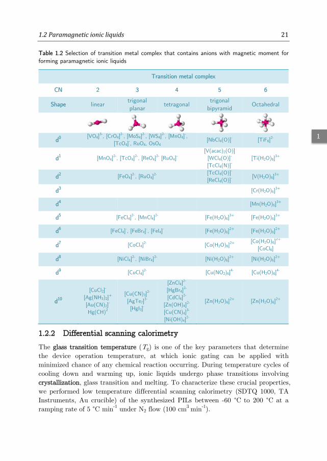
2-, two times molar amount of bulky organic based monovalent halide salts are necessary to realize the designed PIL. Because of the large variety of cations and anions, there is a large group of PILs available as possible gating media. The choice of organic cations includes pyrrolidinium, pyridinium, imidazolium, ammonium, and phosphonium (Tab. 1.1). The anionic metal complex can incorporate all transition metals and some main group metals (e.g. Al, Pb, etc.) and all members of the halogen group (F, Cl, Br, and. I) can compose the metal complex (Tab. 1.2).
1.2Paramagneticionicliquids 21
1
Table 1.2 Selection of transition metal complex that contains anions with magnetic moment for forming paramagnetic ionic liquids
Transition metal complex
CN 2 3 4 5 6
Shape linear trigonal planar
tetragonal trigonal
bipyramid Octahedral
d0 [VO4]3-, [CrO4]2-, [MoS4]2-, [WS4]2-, [MnO4]-,
[TcO4]-, RuO4, OsO4 [NbCl4(O)]- [TiF6]2-
d1 [MnO4]2-, [TcO4]2-, [ReO4]2- [RuO4]- [V(acac)2(O)] [WCl4(O)]- [TcCl4(N)]-
[Ti(H2O)6]3+
d2 [FeO4]2-, [RuO4]2- [TcCl4(O)]- [ReCl4(O)]-
[V(H2O)6]3+
d3 [Cr(H2O)6]3+
d4 [Mn(H2O)6]3+
d5 [FeCl4]2-, [MnCl4]2- [Fe(H2O)6]3+ [Fe(H2O)6]3+
d6 [FeCl4]-, [FeBr4]-, [FeI4]- [Fe(H2O)6]2+ [Fe(H2O)6]2+
d7 [CoCl4]2- [Co(H2O)6]2+ [Co(H2O)6]2+
[CoCl6]
d8 [NiCl4]2-, [NiBr4]2- [Ni(H2O)6]2+ [Ni(H2O)6]2+
d9 [CuCl4]2- [Cu(NO2)6]4- [Cu(H2O)6]4-
d10
[CuCl2]- [Ag(NH3)2]+ [Au(CN)2]- Hg(CH)2
[Cu(CN)3]2- [AgTe7]3- [HgI3]-
[ZnCl4]2-
[HgBr4]2-
[CdCl4]2-
[Zn(OH)4]2-
[Cu(CN)4]3-
[Ni(OH)4]2-
[Zn(H2O)6]2+ [Zn(H2O)6]2+
1.2.2 Differential scanning calorimetry
The glass transition temperature (Tg) is one of the key parameters that determine the device operation temperature, at which ionic gating can be applied with minimized chance of any chemical reaction occurring. During temperature cycles of cooling down and warming up, ionic liquids undergo phase transitions involving crystallization, glass transition and melting. To characterize these crucial properties, we performed low temperature differential scanning calorimetry (SDTQ 1000, TA Instruments, Au crucible) of the synthesized PILs between -60 °C to 200 °C at a ramping rate of 5 °C min-1 under N2 flow (100 cm3 min-1).

22 Chapter1
1
Figure 1.10 shows the distinct behavior found in different PILs depending on their physiochemical properties (melting point, viscosity, coordination number of metal complex, etc.). At room temperature, PILs can exist in liquid, paste, crystal and glass forms. For all measurements, the sample was first cooled down to -60 °C (the lower temperature limit of the instrument) before heating up to 200 °C, where all the PILs were in the liquid form. Melting was observed for those PILs with Tm > -60 °C. The PILs such as BMIM[FeCl4] and P14,6,6,6[FeCl4] show featureless DSC curves indicating that the Tm is below -60 °C, which is suitable for ionic gating at lower temperature.
Figure 1.10 Differential scanning calorimetry (DSC) measurement. Melting temperature (Tm) and glass transition temperature (Tg) are two critical parameters for ionic gating. In order to achieve proper ionic mobility, the gating process is performed slightly above the Tm (Tg) of the ionic liquids. On the other hands, ionic liquids with lower Tm (Tg) are preferred gating media to decrease the kinetics of possible chemical reactions. In our arsenal of PILs, BMIM[FeCl4] and P14,6,6,6[FeCl4] are two candidates with suitable properties.

1.2Paramagneticionicliquids 23
1
1.2.3 Thermogravimetric analysis
Thermogravimetric analysis was used to characterize the high temperature stability of paramagnetic ionic liquids, which is crucial because the gating media are dehydrated by subjecting to heat treatment prior to the gating. We measured the thermal stability up to 500 °C (SDT 2960, TA Instruments) in an Ar protective gas atmosphere (flow rate = 100 cm3 min-1).
Figure 1.11 shows the decomposition of two PILs. Because of the non-boiling character of ILs, the upper temperature limit for applications is given by its thermal decomposition point. The black curve is from a Co2+ based PIL BMIM2[CoCl4], where the ratio between the cation and anion is two. It is clearly seen that two decomposition processes occur above 250 °C.
For the Fe3+ based PIL BMIM[FeCl4], since the ratio of cation/anion is one, there is only one step of decomposition, which occurs at higher temperature (315 °C) than that for PILs with more organic constituents. Organic based cations decompose into small molecules (e.g. CO, H2O, CO2, NOx). Before being applied to the devices for gating, the ionic liquids were typically dried under vacuum at 60 °C for half an hour in order to remove residual H2O. The results of themorgravimetric analysis demonstrate that at this temperature, all the PILs are stable with no concerns regarding the issue of decomposition.
Figure 1.11 Thermogravimetric analysis performed on two different PILs. The black curve corresponds to a Co2+ based PIL where the ratio between cation and anion is two. Consistently, two features corresponding to decomposition appeared above 250 °C. For the Fe2+ based PIL, since the ratio of cation/anion is one, only one decomposition step was observed at a higher onset temperature. All our PILs are stable to at least 200 °C.

24 Chapter1
1
1.2.4 X-ray diffraction measurement
At low temperature, the PILs applied at the interface freeze and crystallize. To estimate the density of molecules at the interface, we determined the unit cell parameters and atomic positions in order to obtain the inter-ionic distances. For PILs with low Tm, in-situ crystallization must be used, simply because the temperature gradient of cooling down is two large and the PILs will form glass instead of crystallizing. Small amount of PIL was introduced under inert gas atmosphere into a fused silica capillary (0.3 mm in diameter), sealed and mounted vertically on a diffractometer. The rest is similar to the Bridgman method; instead, a laser is used for melting the solid locally. Moving laser slowly along the whole capillary from bottom to top for several cycles will turn PIL from glass into single crystal, which is necessary for x-ray diffraction measurement.
The data were collected using a Bruker D8 Venture diffractometer equipped with a monochromator (Triumph) and an area detector (Photon 100). We used Mo Kα radiation and carried out the measurements at 100 K in order to minimize the thermal vibrations. The PILs crystals were picked up using nylon loop with cryo-oil and cooled using a nitrogen flow (Oxford Cryosystems, Cryostream Plus). The diffraction data were processed using the Bruker Apex II software. The crystal structures, as summarized in Tab. 1.3, were solved and refined using the SHELXTL software.
Table 1.3 Unit cell parameters of four typical paramagnetic ionic liquids. The unit cell volume is twice larger of the first three than the last one due to more cations.
Name Space Group
a b c V
(Å) (°) (Å3)
BMIM2[MnCl4] Cc 14.42 9.73 16.95 90 107.59 90 2267.66
BMIM2[MnBr4] C2/c 15.03 9.40 18.71 90 112.36 90 2445.26
BMIM2[CoCl4] Cc 14.39 9.71 16.86 90 107.73 90 2244.06
CMIM[FeCl4] [22] P21/c 9.41 14.65 12.44 90 129.84 90 1317.16
1.2.5 X-ray photoelectron spectroscopy
The oxidation state of the Fe in the PILs was probed by XPS using a Surface Science SSX-100 ESCA instrument equipped with a monochromatic Al Kα radiation (hυ = 1486.6 eV) with 600 μm spot diameter. The spectra were recorded in a vacuum of less than 1×10⁻⁹ mbar with an electron take-off angle of 37° with respect to the sample surface. The energy resolution was 1 eV and 0.2 eV for full and local element spectra, respectively. Binding energies were plotted with respect to the carbon 1s photoemission peak centered at 285.0 eV.

1.2Paramagneticionicliquids 25
1 Figure 1.12 X-ray photoelectron spectroscopy (XPS) of PILs. (a) Full spectrum scanned between binding energies of 1000 eV to 0 eV, indicating the existence of Fe and Cl from paramagnetic FeCl4
- anions. (b) Local spectrum of binding energies from 700 to 740 eV, indicating that the oxidation state of Fe is 3+ (high spin).
Figure 1.12a shows the full spectra of BMIM[FeCl4] on SiO2/Si substrates containing spectral features of all elements composing the PILs. As shown in Figure 1.12b, the chemical environment of Fe is characterized by the Fe 2p1/2 and 2p3/2 peaks of Fe3+ In addition, the pronounced satellite peaks are consistent with the presence of high-spin ferrous species. The high spin state is a prerequisite to enhance the paramagnetic gating with PILs.
1.2.6 Magnetic properties
The magnetic properties of the PILs were measured using a superconducting quantum interference device (SQUID) magnetometer (MPMS XL-7, Quantum Design) in applied fields up to 7 T and at temperature from 2 to 350 K. The temperature dependence of the magnetic susceptibility was measured using zero-field cooling (ZFC) and field cooling (FC) methods. In the ZFC method, the sample was first cooled down to 2 K in zero field and measured in a field of 1000 Oe (or 100 Oe) while warming up. In the FC method, the measurement procedure was identical except that the PILs were first cooled down in a magnetic field of 2 T.
The magnetic susceptibility of each PIL was calculated using Curie’s law. For small magnetic field χ ≪1, where B ≈ μ0H, we have, in CGS units,
3
, (1.20)
where kB = 1.38×10⁻¹⁶ erg K-1, n is the number of magnetic atoms, and χ has in units of emu mol-1 Oe-1.
Theoretically, the effective magnetic moment of the anion is given by 1 , (1.21)
where g is the Landé g-factor, J the total angular momentum, and μB the Bohr magneton, respectively. For 3d metal ion complex, the crystal field is much stronger

26 Chapter1
1
than the spin-orbit coupling; hence the μeff depends only on spin (L = 0, J = S, g = 2).
As shown in Fig. 1.13, the effective magnetic moment per anion of each PIL is calculated from the susceptibility measurements. According to Eq. 1.20, the effective moment obtained from the measurement is μeff ≈ 5.87μB, which agrees well with the theoretical value 5.92 μB calculated from Eq. 1.21. The magnetization is close to the spin-only contribution due to orbital quenching. It is worth noting that both Fe3+ and Mn2+ show high spin states in the magnetic complex anions in PILs, whereas Co2+ is in the low spin state. Despite the Curie behavior for all studied PILs, in each case there are weak antiferromagnetic interactions at low temperature with various strengths.
Below 100 K, signatures of weak antiferromagnetic interactions were observed (Fig. 1.13f) [23]. However, no long range magnetic ordering was established down to 2 K, the lowest temperature accessed in our measurements.
Figure 1.13 Temperature dependence of the magnetic susceptibility of various paramagnetic ionic liquids: [BMIM]2CoCl4 (a), [BMIM]FeCl4 (b), P14,6,6,6FeCl4 (c), [BMIM]2MnCl4 (d), [BMIM]2MnBr4 (e). (f) Summary of temperature dependence of effective magnetic moment per anion for different PILs.

1.3Summary 27
1
1.3 Summary In this chapter, we first introduced the concept of ionic gating technique. In contrast to the conventional solid state gating, ionic gating involves electrochemistry, electric transistor and low-temperature physics, which merge into a unified elegant technique that can modulate the surface state of the gated-materials.
In the second part, we synthesized a group of ionic liquids that possess large magnetic moment. They comprise of large organic cations and complex anions that contains transition metal element. The net unpaired spins of the anion give paramagnetic characteristics of these ionic liquids. We tested the thermal stability of them with DSC and TG measurement. The chemical compositions were characterized via XPS. Moreover, the magnetic properties were measured by MPMS.
In the following chapter 2, 3 and 4, we will apply our synthesized paramagnetic ionic liquids as gating media and utilize the ionic gating technique to study magnetism in low dimension systems.

28 Chapter1
1
1.4 References [1] Zhang Y, Ye J, Matsuhashi Y, Iwasa Y, "Ambipolar MoS2 thin flake
transistors", Nano Lett 12, 1136-40 (2012). [2] Ye J, Craciun MF, Koshino M, Russo S, Inoue S, Yuan H, et al., "Accessing
the transport properties of graphene and its multilayers at high carrier density", Proc Natl Acad Sci 108, 13002-6 (2011).
[3] Nakayama H, Ye J, Ohtani T, Fujikawa Y, Ando K, Iwasa Y, et al., "Electroresistance effect in gold thin film induced by ionic-liquid-gated electric double layer", Appl Phys Express 5, 023002 (2012).
[4] Shimizu S, Takahashi KS, Hatano T, Kawasaki M, Tokura Y, Iwasa Y, "Electrically tunable anomalous Hall effect in Pt thin films", Phys Rev Lett 111, 216803 (2013).
[5] Shimizu S, Takahashi KS, Kubota M, Kawasaki M, Tokura Y, Iwasa Y, "Gate tuning of anomalous Hall effect in ferromagnetic metal SrRuO3", Appl Phys Lett 105, 163509 (2014).
[6] Nakano M, Shibuya K, Okuyama D, Hatano T, Ono S, Kawasaki M, et al., "Collective bulk carrier delocalization driven by electrostatic surface charge accumulation", Nature 487, 459-62 (2012).
[7] Ueno K, Nakamura S, Shimotani H, Yuan HT, Kimura N, Nojima T, et al., "Discovery of superconductivity in KTaO3 by electrostatic carrier doping", Nat Nanotechnol 6, 408-12 (2011).
[8] Shimotani H, Asanuma H, Tsukazaki A, Ohtomo A, Kawasaki M, Iwasa Y, "Insulator-to-metal transition in ZnO by electric double layer gating", Appl Phys Lett 91, 082106 (2007).
[9] Scrosati B, Croce F, Appetecchi GB, Persi L, "Nanocomposite polymer electrolytes for lithium batteries", Nature 394, 456-8 (1998).
[10] https://en.wikipedia.org/wiki/Double_layer_(surface_science) [11] Rogers RD, "Chemistry: Ionic liquids–solvents of the future?", Science 302,
792-3 (2003). [12] Yuan H, Shimotani H, Tsukazaki A, Ohtomo A, Kawasaki M, Iwasa Y,
"High‐density carrier accumulation in ZnO field‐effect transistors gated by electric double layers of ionic liquids", Adv Funct Mater 19, 1046-53 (2009).
[13] Wilk GD, Wallace RM, Anthony JM, "High-k gate dielectrics: current status and materials properties considerations", J Appl Phys 89, 5243-75 (2001).
[14] Miller JR, Outlaw RA, Holloway BC, "Graphene double-layer capacitor with ac line-filtering performance", Science 329, 1637-9 (2010).
[15] Hayes R, Borisenko N, Tam MK, Howlett PC, Endres F, Atkin R, "Double layer structure of ionic liquids at the Au(111) electrode interface: an atomic force microscopy investigation", J Phys Chem C 115, 6855-63 (2011).

1.4References 29
1
[16] Su YZ, Fu YC, Yan JW, Chen ZB, Mao BW, "Double layer of Au(100)/ionic liquid interface and its stability in imidazolium‐based ionic liquids", Angew Chem 121, 5250-3 (2009).
[17] Islam MM, Alam MT, Ohsaka T, "Electrical double-layer structure in ionic liquids: a corroboration of the theoretical model by experimental results", J Phys Chem C 112, 16568-74 (2008).
[18] Bazant MZ, Storey BD, Kornyshev AA, "Double layer in ionic liquids: overscreening versus crowding", Phys Rev Lett 106, 046102 (2011).
[19] Kirchner K, Kirchner T, Ivaništšev V, Fedorov MV, "Electrical double layer in ionic liquids: Structural transitions from multilayer to monolayer structure at the interface", Electrochim Acta 110, 762-71 (2013).
[20] Ye JT, Inoue S, Kobayashi K, Kasahara Y, Yuan HT, Shimotani H, et al., "Liquid-gated interface superconductivity on an atomically flat film", Nat Mater 9, 125-8 (2009).
[21] Hayashi S, Hamaguchi H, "Discovery of a magnetic ionic liquid [Bmim]FeCl4", Chem Lett 33, 1590-1 (2004).
[22] Backer T, Breunig O, Valldor M, Merz K, Vasylyeva V, Mudring A-V, "In-situ crystal growth and properties of the magnetic ionic liquid [C2mim][FeCl4]", Cryst Growth Des 11, 2564-71 (2011).
[23] Del Sesto RE, McCleskey TM, Burrell AK, Baker GA, Thompson JD, Scott BL, et al., "Structure and magnetic behavior of transition metal based ionic liquids", Chem Commun 0, 447-9 (2008).


Submitted to Science Advance: Lei Liang, Qihong Chen, Jianming Lu, Wytse Talsma, Juan Shan, Graeme R. Blake, Thomas T. M. Palstra, Jianting Ye– “Inducing ferromagnetism and Kondo effect in platinum by paramagnetic ionic gating”, 2016 (in review)
Chapter 2
Inducing Ferromagnetism in Platinum by Paramagnetic Ionic Gating
lectrically controllable magnetism, which requires the
field-effect manipulation of both charge and spin degrees
of freedom, has attracted growing interest since the
emergence of spintronics. In this chapter, I will report the
reversible electrical switching of ferromagnetic (FM) states in
platinum (Pt) thin films by introducing paramagnetic ionic
liquids (PILs) as the gating media. Gating using PILs controls
the movement of ions in the presence of adjacent magnetic
moments, which induces itinerant ferromagnetism in Pt films
with large coercivity and perpendicular anisotropy. The field
induced FM state in a non-magnetic metal indicates that
paramagnetic ionic gating can control electric and magnetic
properties simultaneously, which could serve as a versatile tool
to induce transport phenomena contributed by mixed degree
of freedoms at PIL/solid interfaces.
E

32 Chapter2
2
2.1 Introduction
2.1.1 Electrical control of magnetism
It is often accepted that the properties of magnetic materials are settled after been prepared and are not able to be altered afterward. Although enormous successes have been achieved in information technology, such as the discovery of giant magnetoresistance that boosts the development of data storage devices with large capacity, it is mostly based on magnetization reversal while the magnetic medium itself remains unchanged. On the other hand, the ability of externally controlling the properties of magnetic materials would be highly desirable in view of the next generation spintronic devices. Among all possible approaches, electric field control is the simplest and most straightforward approach.
The ongoing quest to control magnetism by electric field has attracted growing interest in both fundamental sciences and technological applications [1-5]. In diluted magnetic semiconductors, switching magnetization can be achieved by modifying the density and type of carriers with external electric field [5-7]. In multiferroic materials, the electric polarization can couple with the magnetization due to exchange striction effects [8-10]. However, both aforementioned approaches require strong electric field and usually reach magnetic ordering below room temperature making them less feasible for applications. The materials showing high Curie temperatures (TC) are generally metallic, which is difficult to manipulate by the field effect due to their intrinsically large carrier densities and consequently short Thomas-Fermi screening lengths. The application of ionic liquids (ILs) on gating (Fig. 1.1) has achieved inducing quantum phase transitions in many insulator [11-13] and semiconductors [14, 15]. Large amount of carriers accumulated by ionic gating can even tune the metallic devices [16-19]. However, so far ionic gating can only gradually vary the metallic FM materials [2, 3, 17], without realizing dramatic changes such as ON/OFF switching of FM states.
2.1.2 Magnetism at molecule/metal interface
The research field of organic spintronics flourishes after the success of fabricating an organic spin-valve [20]. The experiment is based on an organic spacer layer made of π-conjugated organic semiconductor Alq3, which is sandwiched between two ferromagnetic electrodes Co and La0.67Sr0.33MnO3. The results demonstrate that the injection, transport and detection of spin-polarized carrier, which are main ingredients of spintronics, can be achieved through molecular interfaces.
It has been demonstrated as well that the electronic states of non-magnetic materials, such as diamagnetic copper or paramagnetic manganese, is possible to be altered via charge transfer at the metal/C60 interface [21]. Low-energy muon spin spectroscopy indicates localized spin-ordered states at the metal-molecule interface.

2.1Introduction 33
2
Density functional theory further suggests the mechanism to be magnetic hardening of the metal atoms due to electron transfer.
There is also report on forming an antiferromagnetic coupling between paramagnetic Fe-porphyrin molecules and ultrathin ferromagnetic Co and Ni magnetic films on a Cu substrate [22]. This study unveils the possibilities of switching metal-ion spin from antiparallel to parallel respective to the substrate magnetization by spin-polarized current.
Perpendicular magnetic anisotropy of Co is of interest for not only fundamental science but also technological applications. Besides the common method of fabricating Pt/Co bilayer causing interface hybridization of normal metal layer 5d orbital with Co 3d orbitals, organic molecules with π-bond (Pentacene, Alq3, C60) can also react with 3d electrons of Co [23]. The study suggests that this process is governed by the nature of the chemical bonds between the organic molecules and the magnetic electrodes at the interface.
Tunneling magnetoresistance effect has been observed in devices based on molecules, such as zinc methyl phenalenyl that has no net spin. The asymmetric magnetoresistance arises from the independent magnetization switching of the magnetic molecular dimer with respect to the hybridized surface Co layer [24].
To sum up, the formation of chemical bonding at the molecule/metal interface via orbital hybridization between d electrons in metal and molecular π-bonded p electrons serves as an alternative and effective approach to change the electronic and magnetic state of metals once they have been made.
2.2 Concept
2.2.1 Two-dimensional ferromagnetism Magnetism at low dimensionality has been studied extensively and continues to be a subject for its importance in both fundamental and technological interest. Theoretically, a two-dimensional magnet with isotropic short-range interaction does not exist according to the Mermin-Wagner-Berezinskii theorem, which demonstrates that in dimensions d ≤ 2, thermal fluctuations prohibit the long range magnetic ordering at finite temperature in an isotropic system. However, there are a few exceptions of (quasi-) two-dimensional magnets discovered, due to particular parameters.
2.2.2 Stoner criterion of band ferromagnetism Ferromagnetism ultimately stems from the Coulomb interaction. Physically, the Stoner model of band ferromagnets explains spontaneous spin splitting in FM metals such as Fe, Co and Ni, and can be formulated in terms of dispersion relations for spin up and down electrons:
↑↑ ↓, (2.1)
↓↑ ↓. (2.2)

34 Chapter2
2
Figure 2.1 (a) The dispersion relation of a 5d metal showing density of state close to Fermi level. The dash lines denote the Fermi level prior to (brown) and after (black) gating. (b) Density of states showing spontaneous splitting of energy bands without an applied magnetic field. The blue and green colors illuminate the up (↑) and down (↓) spin electrons.
Here, the second term accounts for the exchange energy, where I is the exchange integral, ↑ and ↓ the number of up and down spin electrons, which are given by ↑ ∆ and ↓ ∆ , where N, ρF and ∆EF represent the total number of electron, the density of states at Fermi level and the change of the Fermi energy by electric field, respectively. The situation is illustrated in Figure 2.1.
When gating lifts the Fermi energy from EF to EF*, the kinetic energy gained
is
∆ . (2.3)
However, this process also costs potential energy due to the interaction of the magnetization with the molecular field, given by
12
, (2.4)
in which ↑ ↓ , μ0 and λ are the permittivity and molecular field, respectively. The exchange integral I is a measure of the Coulomb energy, linked to λ by I = μ0μB
2λ. Hence, the total energy change will be
∆ 1 . (2.5)
For spontaneous spin polarization to occur, δE < 0, which requires the product of and I larger than unity:
1. (2.6)
This is called the Stoner criterion.
2.2.3 Hall effect family and anomalous Hall effect
Anomalous Hall effect (AHE) is a member of the Hall effect family. Let us briefly review the history of the discovery of the Hall family members. Edwin H. Hall

2.2Concept 35
2
discovered the ordinary Hall effect in 1879 [25], which he stated when a current-carrying conductor was placed in a magnetic field, the Lorentz force “pressed” its electrons against one side of the conductor. Two years later, he reported that this effect was ten times larger in ferromagnetic iron [26], which was the main character of this thesis: the AHE. Since then, the Hall effect becomes a simple elegant tool to measure carrier type, density and mobility of materials and the AHE is widely used to demonstrate the existence of ferromagnetism. So far, the Hall effects mentioned above require two types of external conditions, which are magnetic field B and magnetization M. Can electric current flow perpendicularly to the electric potential gradient without any external forces? The answer is yes when strong spin orbit interaction is presence.
Spin Hall effect (SHE) refers to such an effect that the spin-up and spin-down carriers accumulate at the opposite edges of the sample without external B field. It was first predicted by Dyakonov in 1971 [27] and was experimentally proved until 2004 [28]. SHE can be regarded as two copies of AHE for carriers with different spin, where both effects are related with the spin-orbit interaction.
Another branch of the Hall family is the quantized version of the Hall effect. In 1980, the integer quantum Hall effect (QHE) was first observed by von Klitzing with strong external magnetic field [29]. The well-defined Hall plateaus manifest the formation of Landau levels caused by B field. When the Fermi level of the systems lies between two neighboring Landau levels, the bulk carriers are localized, while the electron can propagate along the edge of the sample, which is dissipationless and might be useful for fabricating low energy consumption devices.
Figure 2.2 The family tree of the current known Hall effect and the corresponding discovering time.

36 Chapter2
2
Two years later, when the device of two-dimensional electron gas with even higher mobility and at lower temperature down to 0.5 K, the fractional plateaus were found by Daniel Tsui and Horst Störmer [30]. This was interpreted by Robert Laughlin as a new quasiparticle state formed by electrons binding magnetic flux [31].
When the quantized version of Hall effect gets married with its relatives with strong spin-orbit interaction, new offsprings will be generated. The first breakthrough was the discovery of quantum spin Hall effect by Zhang [32] and Molenkamp in 2007 [33], although the concept had been proposed by Kane in 2005 [34] in graphene.
The coming of the last one of the quantized Hall effect trio, the quantum anomalous Hall effect, was a bit late. Previous work focused on the pioneering Haldane model of graphene in a periodic magnetic field with zero net magnetic flux. However, this is too weak to be observed in practical system. In 2013, the emergence of topological insulator opened a new avenue to realize it and eventually it was observed by Que, et al [35].
Among all of the aforementioned members of Hall effect, the understanding of the AHE takes the longest period of time. The reason behind is that the AHE problem involves concepts based on topology and geometry that have been recently formulated. Another reason is that experimentally, the variety of AHE systems is rich and complex.
Figure 2.3 Members of the Hall family. Red and green balls with small arrows denote the electrons with up and down spins. The blue and purple arrows show the direction of the magnetization and external magnetic field directions. The big arrows represent the electron current direction of up and down spins.

2.2Concept 37
2
Reviewing the history of the theoretical studies of AHE, three main mechanisms have been proposed. The first one is the intrinsic mechanism. Initially proposed by Karplus and Luttinger (KL) as the electrons acquire an additional anomalous velocity perpendicular to the electric field [36] and recently formulated by Chang and Niu as the Berry curvature [37].
The KL theory centered on the perfect crystal, whereas another two mechanisms focused on the influence of disorder scattering. In 1955, Smit proposed a theory that ascribed origin of the AHE to the asymmetric scattering from impurities due to spin-orbit interaction [38]. Berger, on the other hand, argued that the electrons experienced opposite electric fields approaching and leaving an impurity [39]. The AHE has become an attractive topic ever since and been reported in numerous systems despite that its physics remains an enigmatic problem until now.
Empirically, the AHE can be described by , (2.7)
where B is the magnetic field, M the magnetization and R0, RA the ordinary and anomalous Hall coefficients, respectively. The first term denotes the ordinary Hall effect and the second term represents the AHE. We will utilize this equation frequently in the following sections and chapters.
2.3 Experiment
2.3.1 Device fabrication and transport measurement
Transistor devices used for PIL gating were all fabricated by standard micro-fabrication. Using electron beam lithography (EBL), we defined a Hall bar of 3×7 μm2. All metal channels (Pt, Pd, and Au) were prepared by DC magnetron sputtering (Kurt J. Lesker) after pumping the chamber below 1.0×10⁻⁸ mbar. Sputtering powers (50 to 200 W) and duration (2 to 12 s) were optimized for preparing films of different thicknesses.
Separately, contact electrodes comprising bilayer Ti/Au (5/70 nm) were deposited onto the patterned Hall bars using e-beam evaporation (Temescal FC-2000) below 1.0×10⁻⁶ mbar. Afterwards, an Al2O3 isolation layer (30 nm) was deposited to cover all contact electrodes, limiting the gating effect only to the exposed channel surface.
Low temperature electrical transports were measured in a helium cryostat (PPMS, Quantum Design) under out-of-plane magnetic fields up to 6 T. All transport properties were measured by two lock-in amplifiers (SR830, Stanford Research) using a constant AC current excitation of 50 μA at 13.367 Hz. The voltage bias on BMIM[FeCl4] (the PIL used in all gating experiments) was applied by a source measure unit (Model 2450, Keithley).

38 Chapter2
2
2.3.2 Paramagnetic ionic liquid
We have introduced the ionic gating technique in chapter 1. Despite the fact that ionic gating is capable of tuning large amount of carriers, it is highly demanding to realize the field-effect control of the spin degree of freedom.
In this chapter, paramagnetic ionic liquids (PILs), composed of anions containing transition metal with unpaired d-orbitals, are introduced as gating media to induce magnetic interactions at the gated channel surface (Fig. 2.4). Therefore, it extends the conventional ionic gating to the spin tunability: the second intrinsic characteristic of the electron.
Replacing the organic anions with metal complexes maintains the general physicochemical properties of ILs, such as low melting temperature (Tm < 200 K), negligible vapor pressure, and large electrochemical window, which are prerequisites for ionic gating. Guided by these crucial requirements, butylmethylimidazolium tetrachloroferrate (BMIM[FeCl4]) was synthesized for all experiments discussed afterwards (Fig. 2.5).
Figure 2.4 Schematic diagram of ionic gating with PIL and transport measurement setup.
Figure 2.5 Composition of PILs: BMIM (cation) and FeCl (anion). The dimensions here were determined from single crystal X-ray diffraction data at 100 K.

2.3Experiments 39
2
2.3.3 Magnetic property
In BMIM[FeCl4], all five 3d orbitals of Fe3+ in the anions are unpaired giving a total spin quantum number of S = 5/2 (high spin state). The temperature dependence of magnetization of BMIM[FeCl4] between 2 to 350 K was measured in a SQUID magnetometer (MPMS XL-7, Quantum Design) up to 7 T. The curves show no hysteresis loop and follow the Langevin equation, indicating paramagnetic nature (Fig. 2.6a). This PIL with considerable large moment (~5.9 μB/Fe3+) responds actively to external magnetic field even at room temperature (Fig. 1.9b).
The temperature dependent magnetic susceptibility (χ-T) measurement was performed after zero-field cooling down to 2 K and the data were taken at B = 0.1 T during warming up. BMIM[FeCl4] shows paramagnetic with large effective moment μeff = 5.87 μB following Curie’s law down to 2 K (Fig. 2.6b).
Below 100 K, signatures of weak antiferromagnetic interactions were observed (Fig. 2.6c) [40]. However, no long range magnetic ordering was established down to 2 K, the lowest temperature accessed in our measurements.
Figure 2.6 (a) Temperature dependence of the magnetization curves for BMIM[FeCl4]. (b) Temperature dependence of the magnetic susceptibility χ. (c) Temperature dependence of the product (χT) of magnetic susceptibility and temperature.

40 Chapter2
2
2.3.4 Paramagnetic ionic gating and temperature dependence resistance
Figure 2.7 shows the transfer curve of the PIL-gated Pt. The gate voltage VG dependence of the sheet resistance Rs (device A, thickness t = 8 nm) shows that the Rs can be reversibly controlled by sweeping VG with negligible leak current IG (Fig. 2.7 bottom panel). The reversible gating response of the sheet resistance Rs is consistent with the linear leak current IG indicating no signature of redox reaction. The electrostatic nature of gating was further confirmed by chronoamperometry experiment (Fig. 1.6) and subsequent control experiments in the supplementary information of this chapter.
Figure 2.7 Typical transfer curve of Pt film (device A, t = 8 nm) with a full gating cycle from -3 to 4 V at a sweeping rate of 50 mV s-1.
Figure 2.8 Cations are driven towards the surface of Pt forming ordered domain patterns after applying positive VG, which leaves the domain interstitials filled with anions [41]. The purple and green arrows denote the spin configuration of the surface and bulk Pt after PIL gating.

2.3Experiments 41
2
After applying positive VG until Rs saturates, cations are driven towards the surface of Pt and form patterns leaving interstitials filled with anions [41] (Fig. 2.8). This surface morphology has a close relation with the formation of magnetic domains in the later sections.
Figure 2.9 shows the five consecutive procedures as a correlation between emergence of ferromagnetism and Rs as a function of temperature. We first applied VG = 4V at 220 K, which is slightly above the frozen temperature of PIL enabling the ionic mobility of ions as well as minimizing the kinetic of side reactions. After observing a prominent Rs drop, device A was cooled down to 2 K at 2 K min-1 followed by the Hall resistance Rxy measurement (showing FM ON state in Fig. 2.9a).
After retracting VG, device A was warmed up to 260 K and Rs coincided with that measured on cooling down until 200 K. With further increasing temperature, the PIL started to melt and Rs gradually increased as the gating effect diminishes with redistribution of the ions. At 220 K, Rs (in red) had exactly the same value as that before gating (in black); this indicates that the whole gating process is non-faradaic. Finally, after fully relaxation of the PIL at 260 K, the device was cooled down back to 2 K without VG and the Hall resistance Rxy was measured (indicating as FM OFF state in Fig. 2.9a).
The emergence of the ferromagnetism is demonstrated by the appearance of hysteresis loop in the AHE at 2 K and will be further discussed in the following sections.
Figure 2.9 (a) Correlation between ferromagnetism and Rs as a function of temperature for five consecutive procedures. (b) Hall resistance Rxy at 2 K with/without applying VG by the procedures described in (a). The FM ON and FM OFF denote Rxy with a hysteresis loop for the FM state and a linear dependence for the PM state.

42 Chapter2
2
2.4 Results and Discussion
2.4.1 Band structure of the ionic gated Pt
Platinum (Pt) is normally regarded as an exchange-enhanced paramagnetic (PM) metal on the verge of FM instability. Hence, applying electric field could induce the FM state in Pt if the enhanced product I satisfies the Stoner criterion, which might subsequently evokes dramatic changes in both magnetism and electrical transport. Meanwhile, decreasing the coordination number of nearest neighboring atoms at the surface results in reduced electronic bandwidth. Consequently, ferromagnetism can be induced when the product of I and is strongly enhanced by reducing dimensionality [42]. For example, although not electrically controllable, the isolated Pt nanoparticles show ferromagnetism if their surfaces are perturbed by chemisorption [43].
According to ab initio calculation, the DOS peak of Pt lies slightly below the Fermi level (EF) [44]. Therefore, it is expected that depleting carriers with negative VG by driving the magnetic anions towards the Pt surface might satisfy the Stoner criterion by increase both and I because of the possible d–d interaction between Pt and FeCl4
-. However, the negatively gated Pt maintains the PM state despite the increase of |Rxy/B| (Fig. S2.1). In contrast, FM states can be induced when the transfer curve shows an obvious drop at VG > 0 (Fig. 2.7), evidenced by the anomalous Hall effect (AHE) with clear hysteresis (Fig. 2.9b). This finding is consistent with other reports of the electric-field tuning of magnetic moments in systems with Stoner enhancement, where a positive VG increases magnetic parameters such as saturation magnetization (Ms), coercivity (Hc) and Curie temperature (TC) [3, 19].
As reported in many other material systems [11, 12], ionic gating can cause significant change of carrier density due to its strong field effect. Here, the apparent carrier density measured by the Hall effect nHall (e.g. extrapolated from Rxy/B) at 5 K significantly increases from 1.68 to 3.24 × 1017 cm-2 upon applying VG = 4 V. Since the actual change of carrier density is caused by the formation of electric double layer, the upper bound of the doping concentration can be simply determined by counting the number of ions accumulated at the channel surface. Direct imaging of ion-gated gold (Au) surface by scanning tunneling microscopy [41] shows that the maximum induced carrier density is limited to ~5 × 1014 cm-2 (Fig. 2.8). Therefore, the large discrepancy between the carrier density estimated from the surface ion concentration and Hall effect indicates that nHall may not be a suitable indicator to quantify the actual change of carriers.

2.4Resultsanddiscussion 43
2
Figure 2.10 Field-effect tuning of EF in the simplified band structure of Pt, where the Fermi surface of pristine Pt is composed of 5d-states at Χ points and the 6s-state near the Γ point in the Brillouin zone. Applying a positive VG lifts the Fermi level (to EF
*) and fills the 5d-band, which changes the conductivity ratio σh/σe significantly.
Despite the quantitative difference, large ∆nHall implies substantial change of EF, which is comprised by the 6s electron-like and 5d hole-like pockets in open and nearly closed Fermi surfaces, respectively [45-47] (Fig. 2.10). Positive VG lifts EF accompanying with the increase of 6s electrons (ne) and decrease of 5d holes (nh). Because of their opposite Hall coefficients, changes of ne and nh contribute destructively to the transverse resistance Rxy [48] causing seemingly large ∆nHall. Because of the elevated EF at VG > 0, the conductivity enhances by having more 6s electrons with higher mobility. More importantly, the increase of EF also reduces the available empty 5d states, causing less s-d scattering [49].
Considering the intrinsically large carrier density in Pt and comparably small change of carriers caused by the field effect, observing large ∆Rs reflects the influence mainly by the reduced ratio of nh/ne. The FM state can be switch ON and OFF by following different sequences of PIL gating as shown in Figure 2.9. The coincidence between the appearance of AHE (Fig. 2.9) and decrease of Rs (Fig. 2.8) indicates a close relationship between the emergence of ferromagnetism and PIL gating.
2.4.2 Perpendicular magnetic anisotropy
Devices that show a perpendicular magnetic anisotropy (PMA) hold promising application in data storage. In metallic thin films, many recipes have been developed. For example, the cobalt film with in-plane easy axis can be converted to PMA when is contacted to platinum [50, 51] or is capped by molecules [23]. Other

44 Chapter2
2
examples include strain-induced PMA in Tm3Fe5O12/Pt bilayer [52] and new materials Mn3Ge [53], CoCrPt [54], etc.
Regarding the determination of magnetic anisotropy of ion-gated Pt thin film, i.e. determining the easy-axis of the magnetization, traditionally, the measurement is based on the magnetization curve from magnetometry (such as SQUID). Sample was measured two times with the basal plane parallel and perpendicular to the magnetic field. Along its hard axis, magnetization of the sample is saturated slowly (Fig. 2.11a); whereas is rapidly along its easy axis (Fig. 2.11b).
However, this type of measurement is limited by the device configuration for PIL-gated systems. In order to measure the perpendicular anisotropy electrically from AHE, a pair of top and bottom electrodes should be attached to measure the Hall effect from in-plane B field (Fig. 2.11c). However, in this case, the top electrode will block the direct contact between PIL and Pt channel. Therefore, no field effect could be applied to the covered surface.
Nevertheless, the square shape of the hysteresis loop with the device geometry shown in Figure 2.11d indicates strong PMA (Fig. 2.9b). Because of the strong screening in Pt, the field-induced modulation is confined beneath the surface within a-few-Å depth. Together with the aforementioned PMA, the induce FM state mimics the ideal two-dimensional (2D) itinerant Ising ferromagnetism.
Figure 2.11 The corresponding hysteresis loops in the Stoner-Wohlfarth model for hard axis (a) and easy axis ∥ (b). Device measurement geometry under in-plane B field (c) and
out-of-plane B field (d).

2.4Resultsanddiscussion 45
2
Magnetic films with PMA are highly pursued in spintronics acting as the exchange bias layers in giant magnetoresistance devices [55], magnetic tunnel junctions [56] and logic devices [57], etc. The gate accessible PMA in PIL-gated Pt is technically favorable because of its electrical tunability.
2.4.3 Temperature-dependent anomalous Hall effect
The temperature dependences of the AHE for PIL-gated Pt films with two thicknesses of t = 8.0 nm (device A) and 2.7 nm (device B) are shown in Figure 2.12. The occurrence of ferromagnetism is manifested as AHE with clear hysteresis loops.
Empirically, the Hall resistivity in ferromagnets can be described by two terms: the ordinary Hall effect and the anomalous part . For the thinner device B, we observed that is one order of magnitude larger than that in device A, indicating a stronger Ms in thinner films. On the other hand, the hysteresis loop of device B is smaller than thicker device A.
Figure 2.12 Temperature-dependent Hall resistivity in FM Pt after PIL gating. Both device A with t = 8.0 nm (a) and device B with t = 2.7 nm (b) show a deceasing and with increasing temperature, while are different in the amplitude of and the slope of the linear part of .

46 Chapter2
2
The coercive force disappears rapidly for both samples while the saturation magnetization maintains up to quite high temperature (>160 K). In addition, the magnetization direction is the same for both samples while the slope of the linear part of the Hall effect is opposite for each sample. The sign of the ordinary Hall coefficient indicates the difference of the Fermi surface topology, which remains to be understood with further experimental and theoretical studies.
2.4.4 Gate-dependent anomalous Hall effect
It is worth noting that the strength of the induced FM states are closely linked to the VG (Fig. 2.13). As shown in Figure 2.13b, the AHE measured for the same device at 5 K shows gradual decrease of the and Hc after being cooled down with different VG biases reduced from VG = 4 V, which is consistent with the increase of ordinary Hall coefficient R0 demonstrated in 3.4.1.
The electrostatic nature of the gating is further validated by measuring the AHE at 5 K for the same device cooled down with different VG (Fig. 2.13a). The change of Rs with respect to VG is defined as
Δ 0 , (2.8)
where Rs(VG) and Rs(0) are the Rs at finite and zero VG, respectively. Figure 2.13a shows a typical VG dependence of Rs at 220 K with a full bias sweep from -3 to 4 V. Clear resistance drop appears under positive gating, which is consistent with other reports [58, 59].
We performed the Hall measurement at different VG in a typical film (t = 16.0 nm) under out-of-plane magnetic field at 5 K. For achieving each electronic state, the device was first gated to 4 V at 220 K when the Rs approaching saturation. Afterwards, we gradually decreased VG to the desired values by monitoring the change of Rs. The low ionic mobility at 220 K leads to a hysteretic VG dependent Rs (Fig. 2.13a). Therefore by decreasing VG, we can realize better control to reach the desired electronic state by minimizing the change of Rs before actually frozen of PIL.
To measure the Hall effect at five different VG as shown in Figure 2.13b, we first gated sample to VG = 4.0 V, which induced the hysteresis loop in AHE at 5 K indicating the existence of ferromagnetism. The sample was then warmed up to 260 K with VG = 0 V and cooled down to 220 K for repeating identical gating process. With the decrease of VG, the hysteresis loop in (at 5 K) gradual diminished and evolved into a linear dependence of B, indicating the switching off of the FM state. This order of measurement sequences excludes the possibility of forming impurities by the previous gating. Following the continuous tuning of the FM states, the slope of the linear part of the Hall signal observed at high B field increase with the decrease of VG suggesting a continuous tuning of carriers. On the other hand, the gradual evolution and repeatable access of FM state strongly suggest that the FM state depends on the applied VG, which is free from magnetic impurities accumulated or reversible, formed by all prior gating procedures.

2.4Resultsanddiscussion 47
2
Figure. 2.13 Gate-dependent Hall resistivity in FM Pt after PIL gating. (a) The transfer curve with red dots showing the gated states that have been cooled down. (b) The corresponding AHE effect measured at 5 K for each gated states. (c) The correlation between the VG, that represents the saturation magnetization and the slope of ordinary Hall effect 1/RH that stands for the change of the carrier number.
2.4.5 Thickness-dependent anomalous Hall effect
As shown in Figure 2.14, the film thickness dependence of indicates that the increases with the decrease of t. For films with t > 24.0 nm, the AHE signal
cannot be distinguished from the linear because the short screening length isolates the gating effect from affecting the bulk of gated Pt films, which remains PM with linear Hall response. With the increase of t, the enlarging bulk contribution acts as a short circuit channel bypassing the top-most FM layer resulting the reduction of .
Figure 2.14 The thickness-dependent Hall resistivity as a function of B for several Pt films.

48 Chapter2
2
Despite the larger in thinner films, the largest Hc was observed for t = 8.0 nm. Since the Hc is closely related to the formation of magnetic domains in different film morphologies, the optimization of the density and rigidity of domain walls at this intermediate thickness might give rise to the largest Hc.
In addition, the ordinary Hall coefficient changes sign at t = 2.7 nm. These observations indicate a modification of the band structure with decreasing thickness, which enhances the Stoner instability in Pt (Pd) films [60].
2.4.6 Strong spin-orbit interaction
Since Pt is a heavy metal, besides the Stoner criterion, we should also take into account the effect of the spin-orbit interaction (SOI). The SOI in an atom arises as follows. Consider an electron orbiting a nucleus; from the electron point of view, the orbiting nucleus constitutes a current that gives rise to a magnetic field (from Biot-Savart law) equal to
4
, (2.9)
where Z is the atomic number, e the elementary charge, μ0 the vacuum permeability, m0 the elementary mass of electron, r the radius of the orbit.
In addition, the magnetic moment by electron spin is given by
2
, (2.10)
where g is the Landé g-factor. Therefore, the spin-orbit energy can be represented as
12 ∙
8∙ . (2.11)
On the other hand, the total angular momentum operator is given by . (2.12)
Taking the dot product of with itself, we have 2 ∙ . (2.13)
So the total angular momentum can be described in terms of quantum numbers:
∙12
∙ ∙ ∙2
1 1 1 , (2.14)
where s, l, j are the spin, orbital and total angular quantum number, respectively. Taking Eq. 2.14 back to Eq. 2.11, we get
1 1 1 , (2.15)
where the spin-orbit interaction constant a is defined as
16
, (2.16)
Substituting ⟨ ⟩ , ,∗
, , from the expectation value of hydrogen wave function, we derive
∝1 2⁄ 1
, (2.17)

2.4Resultsanddiscussion 49
2
Figure 2.15 (a) Longitudinal magnetoresistance of device B with (red) and without (blue) . (b) Corresponding transverse (Hall) resistance of the same device B in PM (OFF) and FM (ON) states at 5 K.
which implies that the strength of SOI: is proportional to the fourth power of atomic number; decreases with increasing quantum number n and l.
Pt is widely used in spintronic devices due to its strong intrinsic SOI and resulting large spin Hall angle θSH. Although AHE was discovered prior to SHE, the former can actually be regarded as two copies of the later, where relativistic spin-orbit coupling generated an asymmetric deflection of the charge carrier depending on their spin direction [61]. The pristine Pt films show weak anti-localization (WAL) due to the intrinsically large SOI, resulting in the positive magnetoresistance (blue curve in Fig. 2.15a) [62]. When the FM state is switched ON, a negative magnetoresistance appears at low temperature because applying B field in FM state increases the degree of spin polarization hence reduces s-d scattering (red curve in Fig. 2.15a). This significant change of the longitudinal transport after gating accompanies with the appearance of the AHE in the transverse measurement (Fig. 2.15b).
Figure 2.16 Low temperature (T < 40 K) magnetoresistance of (a) pristine, (b) IL-gated (DEME-TFSI), and (c) PIL-gated (BMIM[FeCl4]) Pt films (t = 4.0 nm).

50 Chapter2
2
DFT calculation reveals that the Rashba splitting in the heavy metal surface states can be effectively manipulated by shifting the d-orbital potential energy by physical implementation [63]. Although compared to the Coulomb field inside the atom, the electric field generated by the electric double layer is weak. However, due to the large SOI of Pt, Rashba effect is another factor to be considered.
To show the different electronic states, we measured the MR below 40 K for pristine, IL-gated, and PIL-gated devices that are all made from a single Pt film (t = 4.0 nm). As shown in Figure 2.16a, the pristine Pt film shows positive MR, which is originated from the WAL due to the strong spin-orbit interaction in Pt. Almost identical MR (Fig. 2.16b) was observed after gating the same Pt film with a typical non-magnetic ionic liquid (N,N-diethyl-N-(2-methoxyethyl)-N-methylammonium bis(trifluoromethylsulphonyl-imide (DEME-TSFI, widely used for ionic gating) in absence of FM state. In contrast, the PIL-gated Pt film shows negative MR in same temperate range (Fig. 2.16c). We ascribe the negative MR to the induced interface ferromagnetism. The intrinsic WAL in Pt and WL caused by interface magnetization causes the WAL to WL crossover as a function of temperature.
2.4.7 Crossover between weak localization and weak anti-localization
Inducing FM states naturally affects other transport properties of Pt, such as the magnetoresistance. The conductivity of conduction electrons σ is determined by the scattering rate, given by
∗ , (2.18)
where n and m* are the electron density and effective mass, respectively; τ is the relaxation time of electron and links the electron mean free path λ with λ = kFτ (kF is the Fermi wave vector), which is influenced by impurity scattering, electron-phonon and electron-electron (Coulomb) interaction.
However, the above semi-classic quasi-particle model ignores the interference of the electron waves. The impurity scattering strength is independent of temperature and screening effect of conduction electron compensates the Coulomb interaction. At low temperature, therefore, when the phonon contribution is minimized, interference effect of the electron wave also plays important role and have a quantum correction yielding the conductivity
11
ln ln , (2.19)
where τ0 and τi are the elastic and inelastic scattering time, respectively; and σ00 = e2 / (πh).
Applying magnetic field B will induce a magnetic flux ΦB. When B > ΦB, those quantum interference will be destroyed, resulting a negative magnetoresistance (hence positive magnetoconductance). This is called weak-localization (WL) effect. The weak anti-localization (WAL) originates from the

2.4Resultsanddiscussion 51
2
strong SOI, which randomizes the electron spins, resulting in a positive magnetoresistance (hence negative magnetoconductance).
The aforementioned electron localization behavior can be well reproduced by the Hikami-Larkin-Nagaoka (HLN) equation [64]. In the low field regime, the conductance variation is given by
Δ 01 1
0
(2.20)
2ln
12
ln12
32
ln4 3⁄ 1
2
4 3⁄
where ψ is the digamma function, Bϕ, BSO and Be are the characteristic field Bi linked to characteristic lengths li (distances) of phase coherence, electron traveled before being disturbed by spin-orbit interaction and elastic mean free path, respectively, by /4 .
In the limit of strong SOC, Eq. 2.20 reduces to
Δ2
ln12
(2.21)
where α is a coefficient indicating the type of localization, namely α < 0 for weak localization and α > 0 for weak anti-localization [64]. For the thinnest film (t = 2.7 nm, device B) in which the surface contributes the most, we analyzed the effect of FM states on the longitudinal magnetoconductance (MC). The temperature variation of ∆G(B)=G(B)-G(0T), exhibits a crossover between WAL and WL at low B field region due to the competition between thermal fluctuations kBT and spontaneous magnetizations that randomize and align the orientation of magnetic moments, respectively (Fig. 2.17a).
Figure 2.17 (a) Fitting the temperature dependence of the magnetoconductance of device B by the Hikami-Larkin-Nagaoka (HLN) equation. (b) Correlation between the α prefactor (black) used in the HLN equation and saturation magnetization Ms (red) derived from the AHE.

52 Chapter2
2
Table 2.1 Fitting parameters with HLN equation of the low field magnetoconductance data at various temperatures
T (K) 5 10 20 40 80 120 160
α 0.085 0.085 0.078 0.047 -0.006 -0.050 -0.089
Bϕ (T) 0.051 0.051 0.052 0.053 0.028 0.055 0.064
lϕ (nm) 56.85 56.85 56.30 55.77 76.32 54.87 50.89
We next turn to a more quantitative analysis of the observed MC crossover
phenomena. Considering our gating effect is a surface effect, hence the induced ferromagnetism as well as other transport phenomena should be confined within two dimensions. Applying HLN equation to analyze this crossover behavior, we derived that the temperature dependence of the fitting coefficient α scales linearly with the anomalous Hall resistance , demonstrating a close correlation between the electrical transport and the magnetization M at the surface of Pt films (Fig. 2.17b). This crossover resembles the behavior observed in magnetically doped topological insulators, where the surface states are also affected by the magnetization [65]. Consistently, the phase coherence length (lϕ ~50 nm) extracted from the HLN fitting (Tab. 2.1) is comparable with other surface magnetization systems [62, 65, 66].
Having a closer look at MC data in the full B field range (Fig. 2.18a), we notice that the profile of the B dependence is highly nonlinear. At low field range (|B| < 2 T), it shows crossover of MC, from positive MC at low temperature to negative MC at high temperature. At high field range (|B| > 4 T), the MC shows linear dependence on B field. At low temperature, the MC at high field shows positive slope. With the increase of temperature, this high field slope gradually decreases and becomes almost flat. For both variations in high and low field features, there is a transitional region between 2 T < |B| < 4 T.
Figure 2.18 (a) The longitudinal transport data of Pt thin film of t = 2.7 nm. (b) Schematic illustration of the PIL-gated Pt device. It contains two interfaces, which are the PIL/topmost ferromagnetic (FM) Pt interface and the topmost FM Pt/bulk paramagnetic (PM) Pt interface.

2.4Resultsanddiscussion 53
2
The reason of complex transport data in our system is mainly due to mixture of localization with other transport phenomena. The system contains electronically dissimilar topmost layer gated by PIL and bottom unperturbed film that maintains the intrinsic bulk properties of Pt. Moreover, it is worth noting that the transport might also be affected by the interfacial behavior between these two layers (Fig. 2.18b). Due to the strong screening effect in intrinsic metal, the bulk Pt beneath the topmost layer behaves as pristine Pt, showing the same positive MR (negative MC) as shown in Figure 2.17a. A very important point here is the temperature range. The MR of pristine Pt only persists up to 40 K, from which the MR becomes featureless. Therefore, large MR response even at 160 K is due to the surface state.
The top-most Pt becomes FM after being gated with PIL, showing a positive linear MC at large field. With increasing of temperature, the ferromagnetism gets weaker and this positive MC diminishes as well. The same behavior happens for thicker film as well, despite that at low temperature the negative MR is less observable, due to larger mixing of the positive MR from the bulk Pt (intrinsic WAL). However, at higher temperature, the positive MR is purely due to the surface Pt because the bulk shows nearly zero MR (Fig. 2.16a).
2.4.8 Scaling relationship of anomalous Hall effect in PIL-gated Pt and various other systems.
Quantitatively, the origin of the AHE can be analyzed by the scaling relationship between anomalous transverse resistivity (conductivity) ρAH (σAH) and longitudinal resistivity (conductivity) ρxx (σxx) in a power law form ρAH ∝ ρxx
γ [67]. The components of the conductivity tensor were derived by inversion of the resistivity tensor. For cubic symmetry, which is valid for the face-centered cubic structure of Pt and B ∥ c, we get , 2.22)
and , (2.23)
Here, ρAH is determined by extrapolating ρxy in the linear regime to zero field. Figure 2.19 shows the scaling diagram of anomalous Hall effect in PIL-gated
Pt compared to various other systems. Different kinds of markers denote the σxx and σAH for distinct systems while each marker of the same kind represents the value at various temperature. When γ = 1, i.e. ρAH ∝ ρxx (σAH ∝ σxx), the skew scattering mechanism dominates [38]; whereas the case of γ = 2, i.e. ρAH ∝ ρxx
2 (σAH ∝ const.), corresponds to the side jump mechanism [39]. The γ components in both of these extrinsic origins are temperature dependent.
Our PIL-gated Pt, however, displays a scaling relation σAH ∝ σxxγ (γ ≫ 1)
that is different from any other system (Fig. 2.19). One reason is because Pt is a

54 Chapter2
2
metal so that the electrical conductivity σxx does not change too much with temperature. On the other hand, the amplitude of the anomalous Hall effect that corresponds to the strength of the ferromagnetism changes rapidly with varying the temperature, which causes a significant variation of σAH. With increasing temperature, σAH decreases significantly, which is distinct from the situation in conventional band ferromagnets [68].
Figure 2.19 Scaling diagram of AHE for various magnetic systems. The AHE measured in PIL-gated Pt samples (shaded by yellow) are plotted together with many magentic systems reported previously [73-76]. The measured for the FM state of Pt shows weak dependence on the .

2.4Resultsanddiscussion 55
2
In addition, the behavior of with respect to temperature strongly relies on the gating level VG, which affects not only the change of σxx, but also σAH. The fact that σAH appears to be independent of σxx indicates that the induced ferromagnetism in Pt is intrinsic [69, 70]. When Pt is in the vicinity of a FM insulator, yttrium iron garnet (YIG), the AHE induced by the magnetic proximity effect (MPE) shows the opposite B field dependence, because the induced magnetic moments are anti-parallel to the magnetization of YIG [71, 72]. In contrast, the magnetization direction of the present system follows the B field. Both systems show the reversal of the ordinary Hall coefficient for ultrathin Pt films (t < 3.0 nm), which is consistent with the significant change of the band structure at reduced-dimensionality. In contrast to YIG, the strong Coulomb repulsion between anions in PIL sets large interionic distance, which prohibits FM exchange interaction. Hence, BMIM[FeCl4] remains PM down to 2 K (Fig. 2.6b), which firmly excludes the MPE as the origin of the reported phenomena.
2.4.9 Magnetic phase diagram of PIL gated Pt
We determine the saturation magnetization of the PIL-gated Pt by extrapolating the linear part of Rxy under high B fields, where the anomalous Hall resistance Rxy
A that represents the Ms can be extracted (Fig. 2.20). The temperature dependence of Ms can be described by the Bloch equation
0 1 , (2.24)
where Ms(0) is the spontaneous magnetization at T = 0 K and β is the Bloch constant [77]. Fitting Ms for the film with t = 2.7 nm and thicker films (t = 8.0, 12.0, 16.0 nm) yielding β = 1.3 and 1.8, respectively. The similar β and resembling behavior of Rxy
A indicate that all FM samples of different thicknesses are likely originated from the same type of magnetization.
In general, Tc decreases with the increase of t. For sample A (t = 8.0 nm) optimized for the largest Hc, the extrapolated Tc is even above room temperature (300 K). In fact, the Tm of BMIM[FeCl4] limits the upper-bound temperature of the induced FM state. Alternatively, choosing PILs with higher Tm might enable room temperature FM switching.
Interestingly, at low temperature (< 40 K), the Ms deviates from the Bloch equation, exhibiting an up-turn in accordance with the 1/T dependence. This behavior signals an effective field between the FM Pt layer and the paramagnetic FeCl4
- anions within the mean field theory, whose PM magnetization significantly increases at low temperature obeying Curie’s law. It is worth noting that applying the same gating protocol to the identical Pt films using a conventional IL shows no ferromagnetism despite of the increased electrical conductivity (Fig. 2.16, Fig. S2.5) [58]. This clear difference indicates the importance of PIL in inducing the FM state in Pt.

56 Chapter2
2
Figure 2.20 Magnetic phase diagram of Ms versus T jointed for gated Pt films of different thicknesses. The left panel indicates the ultrathin Pt film (t = 2.7 nm) with a positive ordinary Hall coefficient R0. The right panel shows data from four individual thicknesses (8-24 nm), which all have a negative R0. Gating effect becomes vague for films thicker than 16 nm. Ms of most temperature range follows the Bloch Law. At T < 40 K, Ms with R0 < 0 displays an anomaly that can be fitted by Curie’s law.

2.5Supplementaryinformation 57
2
2.5 Supplementary information
2.5.1 Transport properties under negative ionic gate bias
We also measured the transport properties induced by negative VG (Fig. S2.1). Negative gating accumulated magnetic anions on the surface of Pt film. Due to the strong screening of a typical metal, the accumulated anions deplete electrons at the top-most layer of Pt film. If AHE was mainly induced by exchange interaction between the carrier and the local moment of magnetic anion, the negative gating should induce even more pronounced FM state.
Conversely, negative gating only changes the slope |Rxy/B| of linear Hall effect without inducing AHE (Fig. S2.1a). Moreover, the positive MR measured for negative VG (Fig. S2.1b) is similar to that observed for pristine Pt (Fig. S2.1a), which is consistent with the absence of FM states.
Figure S2.1 (a) Negative VG decreases EF, which increases the number of empty states in the 5d-band. In the transfer curve, the conductivity decreases due to more s-d scattering. Because of the opposite sign of nh, the Hall conductivity Rxy changes consistently with different VG. The Hall coefficients at 5 K change oppositely for positive VG (brown) and negative VG (orange) with respect to the pristine state (black). (b) In contrast to the negative MR in the positively gated state, the MR of the negatively gated sample behaves similar to its pristine state: positive MR at low temperature, which diminishes rapidly with increasing temperature. No ferromagnetism can be induced with negative VG.

58 Chapter2
2
2.5.2 Transport properties of PIL-gated gold thin film
Gold (Au) is the element next to Pt with one more 5d-electron, which fully fills the 5d-band. Identical PIL gating was applied on Au film with t = 8.0 nm (Fig. S2.2a). The temperature dependence of Rs in five consecutive procedures was shown in Figure S2.2c: (1) Apply VG at 220 K. (2) Cool device down to 2 K at 2 K min-1 and measure Rxy (state I ). (3) Warm device up to 260 K at VG = 0; the Rs coincided with the cooling down curve at VG = 3 V until the ions become mobile again. At 220 K, the Rs (in red) has exactly the same value as that before gating (in black), indicating that the whole gating process is non-faradaic. (5) After fully relaxing the PIL at 260 K, the device was cooled down to 2 K without VG. The Rxy was again measured at 2 K (state II).
Compared with Pt film of similar thickness, significant decrease of Rs at VG > 0 was also observed. In spite of the similar VG dependence of Rs, neither AHE (Fig. S2.2d) nor Kondo effect (chapter 3) (Fig. S2.2b) was observed in PIL-gated Au down to 2 K. The absence of FM state in Au after PIL gating is consistent with its fully filled 5d-band and the band-filling scheme mentioned in Fig. 2.10.
Figure S2.2 (a) Transfer curve of Au gated with a VG sweep rate of 50 mV s-1 between 4 and -3 V. (b) Normalized sheet resistance Rs in the low temperature range shows no Kondo signature. (c) Temperature dependence of Rs in five consecutive procedures. (d) The Hall effects measured at state I and state II reveals that Au film does not show any clear AHE feature regardless of applying the VG.

2.5Supplementaryinformation 59
2
2.5.3 Transport properties of PIL-gated palladium film
Beside Pt and Au, the identical PIL gating was also applied to palladium (Pd), another typical exchange-enhanced metal. As shown in Fig. S2.3, the PIL gating of a Pd film (t = 5.0 nm) can also induce FM state. Comparing with the Pt film of similar thickness, we briefly summarize the major consistent behaviors as follows: 1) At low temperature (5 K), the pristine or unbiased (VG = 0) Pd film shows
positive MR (Fig. S2.3a) and ordinary Hall effect (Fig. S2.3c). 2) PIL gating switches the MR from positive to overall negative MR after the
emergence of AHE (Fig. 2.3b). 3) The PIL gating induces FM state with clear coercive loop in AHE (Fig. 2.3d).
In spite of the similarities, quantitatively, the MR of PIL-gated Pd shows much more pronounced hysteresis in the low field regime (Fig. 2.3c), where the AHE effect also shows hysteresis loop (Fig. S2.3d).
Figure S2.3 Low temperature (T = 5 K) electrical transport of pristine and PIL-gated Pd thin films. (a) Pristine Pd film shows a weak anti-localization in MR. (b) Pristine Pd shows ordinary Hall effect. (c) Longitudinal MR shows butterfly-shaped hysteresis due to FM state. (d) The Hall effect measurement shows AHE with a hysteresis loop within ±2 T, in consistent with the size of hysteresis found longitudinal MR.

60 Chapter2
2
The clear butterfly shape in MR indicates the randomization of magnetic domains close to the switching of the magnetization direction. On the other hand, the hysteresis loop in AHE (Fig. S2.3d) is smaller compared to Pt. The strength of spin-orbit interaction (Eq. 2.17) in Pd is ~4.78 time smaller than Pt, which might play a role in the different AHE behavior [78, 79].
Nevertheless, inducing FM state also in Pd indicates the universality of the PIL gating technique as an effective methodology for inducing FM states. The full results will be detailed in an independent paper. Despite the quantitative differences, the highly consistent FM state suggests that our proposed physical picture might be universal to Stoner enhanced elements.
2.5.4 Transport properties of Pt thin film doped with Fe impurity
Figure S2.4 Comparison between Fe impurity-doped and PIL-gated Pt thin films. (a) Temperature dependence of sheet resistance at low temperature on a linear scale. (b) Temperature dependence of sheet resistance at low temperature on a logarithmic scale. The Pt sample with Fe impurities does not show a Kondo effect, which is in sharp contrast with both gated counterparts. (c) The anomalous Hall signal observed in the sample with Fe impurities is negligibly small compared with the PIL-gated systems. (d) The MR of the sample with Fe impurities is also distinct from those measured for PIL-gated Pt films, in which the former shows a positive MR with weak localization behavior in small fields, while the latter shows negative MR.

2.5Supplementaryinformation 61
2
To firmly remove the possibility of having trace of Fe impurities after PIL gating, we prepared a Pt film with Fe impurities (0.2 nm nominal thickness) intentionally evaporated in-situ prior to the deposition of Pt film. Compare to the PIL-gated Pt film of identical thickness (8.0 nm), the Pt film with Fe contamination shows negligibly weak ferromagnetism (Fig. S2.4a).
The Fe/Pt film shows negative MR at small B field (|B| < 1 T), indicating typical weak localization behavior. This is consistent with the presence of Fe impurities (red curve in Fig. S2.4b). Under larger field (|B| > 1 T), the positive MR is consistent with the conventional dependence of Rs ∝ μB2. In contrast, the MR of PIL-gated Pt film shows distinct behaviors. There is a clear crossover from positive to negative MR with the decrease of film thickness. The very thin film (t = 2.7 nm) shows negative MR (blue curve in Fig. S2.4b), while the thicker Pt films (t > 8 nm) show positive MR. Since the PIL gating only affects the surface of the Pt films, the MR of the bulk remains positive regardless of the film thickness. Therefore, thinner film has less contribution from the bulk positive MR. The featureless MR observed for film of t = 8.0 nm might come from the compensation between these two opposite MR dependences (green curve in Fig. S2.4b).
In addition to the contrasting magnetization and MR dependence, the Fe doped Pt film shows no Kondo effect at low temperature (Fig. S2.4c,d). We will discuss more about the Kondo effect in chapter 3.
In summary, contaminating the Pt film by introducing Fe impurities cannot reproduce the effect of PIL gating, which suggest that the gate induced FM state cannot be ascribed to Fe contamination.
2.5.5 Gating cycles with sequential switch between PIL and conventional IL
As a control experiment for clarifying what are the essential ingredients for inducing FM state, we performed gating cycles by switching the gating media between conventional IL that contains non-magnetic ions (DEME-TFSI) and PIL (BMIM[FeCl4]) on the same Pt film (t = 12.0 nm). As shown in Fig. S2.5, a series of measurements shown in panel A to E is grouped in different step 1 and 2 for gating with IL and PIL, respectively. Therefore, each measurement on the sequential change of sample status can be easily tracked by labeling cycle/step/panel in the matrix (Fig. S2.5).
For gating with both IL (C1/S1/B) and PIL (C1/S2/B), although the VG dependence of the Rs show similar substantial decrease with the increase of VG, the AHE from FM state was induced only by the PIL gating (red line, C1/S2/D) in contrast to the ordinary Hall effect (C1/S1/D) observed by IL gating. To confirm that this FM state exists only after gating, we warmed the sample gated by PIL (C1/S2/D) up to the melting temperature of the PIL with VG = 0 V (following the red line of C1/S2/C) to release the gating effect. Then the device was cooled down to 5 K again with VG = 0 V (following the blue line of C1/S2/C). The Hall effect

62 Chapter2
2
measured thereafter shows linear field dependence without AHE (blue line, C1/S2/D). To remove the concern about the possible FM impurities produced by the PIL gating, we repeated IL gating on the same device immediately after washing away the PIL by acetone (C1/S2/E). The Hall signal (C2/S1/D) resumed the linear field dependence without AHE feature in consistent with the status access by the identical gating conditions using IL (C1/S1/D). By switching back to PIL, the FM state can be repeatedly induced as shown by the clear AHE signal (red curve, C2/S2/D). Again, melting the PIL can restore the linear Hall response (blue curve, C2/S2/D).
Figure S2.5 Diary of gating cycles by switching the gating media between non-magnetic IL and PIL on the same Pt film (t = 12.0 nm). (a) Schematic molecular structures of used ILs. (b) The VG dependence of Rs for each gating procedure. (c) Temperature dependence of the Rs measured after each gating. (d) The Hall effect measured at 5 K after each cooling down, where the different color matches the color of temperature dependence of Rs of the cooling procedure (red for VG > 0, blue for VG = 0). (e) Optical images taken after each measurement. The ionic liquid was washed away by acetone and the device was cleaned by isopropanol.

2.5Supplementaryinformation 63
2
In conclusion, the reversible behavior observed in consecutive gating cycles using different liquids not only clearly shows the indispensable role of PIL gating but also excludes Fe contamination as the possible origin of the induced FM state.
2.5.6 Optical and atomic force microscopy of Pt film before and after gating
The sample status at each step of the gating cycles is closely monitored by optical and atomic force microscopy (AFM) as shown in Figure S2.5e and Figure S2.6a, b. The AFM images are all measured in tapping mode (Bruker Nano MultiMode 8-HR) for characterizing the surface morphology and sample thickness.
Figure S2.6 Surface morphology of Pt film before and after PIL gating. Optical images of the Pt sample before applying the PIL (a) and after gating with the PIL (b). In both panels (a) and (b), the scale bars correspond to a length of 5 μm. AFM imaging of the Pt film surface were performed within the areas marked by red dots. Along the yellow line in panel (c), the height profile (white) of the film shows that the thickness of the film is 12.0 nm. The surface morphology is shown for the areas within green rectangles in panel (c) and (d) for the sample before (e) and after (f) PIL gating. Corresponding bird’s eye views of the surface morphology are also shown before (g) and after (h) PIL gating. It is worth noting that most of the fine details of the sample remains identical before and after gating.

64 Chapter2
2
For the Pt sample of t = 12.0 nm (Fig. S2.6c), the root mean square (Rms) of the surface roughness from 1×1 μm2 scanned area was 1.7 nm (Fig. S2.6e, f). The surface roughness is closely related to the deposition technique and the flux rate. In general, magnetron sputtering produces films with better crystallinity but rougher surface compared to the film prepared by e-beam evaporation [80]. For all Pt films measured before and after gating, no clear difference could be resolved for the morphology of Pt surface (Fig. S2.6e, f, g, h).
2.6 Summary In this chapter, we study the paramagnetic ionic gating induced ferromagnetism in Pt thin film comprehensively, revealed as anomalous Hall effect (AHE). By introducing the paramagnetic ionic liquids as gating media, we demonstrated that ferromagnetic state can be reversibly switched ON and OFF in Stoner enhanced element, such as Pt and Pd.
The induced ferromagnetic state has been proven to be two-dimensional (2D), evidenced by the crossover behavior of the electron localization in the magnetoconductance measurement for the thinnest film.
With increase of the film thickness, the enlarged bulk conduction acts as short circuit bypassing the surface channel, which diminishes the ferromagnetic signal, such as anomalous Hall effect and negative magnetoresistance.
A series of control experiments have firmly confirmed the electrostatic nature of the gating, in which magnetic impurities should not be the reason causing the emergent surface spontaneous magnetization.
The magnitude of induced FM state depends on the gate voltage as well as temperature. From the fitting of the temperature dependence of saturation magnetization, the Curie temperature can exceed the room temperature.
Although an explicit fundamental theory remains an open issue, phenomenologically, the emergence of the 2D ferromagnetism in Stoner exchange metal thin film requires the combination of large charge accumulation in presence of paramagnetic moments. Scaling analysis of the AHE proves the intrinsic origin of the FM state.

2.7References 65
2
2.7 References [1] Ohno H, Chiba D, Matsukura F, Omiya T, Abe E, Dietl T, "Electric-field
control of ferromagnetism", Nature 408, 944 (2000). [2] Weisheit M, Fahler S, Marty A, Souche Y, Poinsignon C, Givord D,
"Electric field-Induced modification of magnetism in thin-film ferromagnets", Science 315, 349-51 (2007).
[3] Chiba D, Fukami S, Shimamura K, Ishiwata N, Kobayashi K, Ono T, "Electrical control of the ferromagnetic phase transition in cobalt at room temperature", Nat Mater 10, 853-6 (2011).
[4] Matsukura F, Tokura Y, Ohno H, "Control of magnetism by electric fields", Nat Nanotechnol 10, 209-20 (2015).
[5] Chiba D, Yamanouchi M, Matsukura F, Ohno H, "Electrical manipulation of magnetization reversal in a ferromagnetic semiconductor", Science 301, 943 (2003).
[6] Dietl T, "A ten-year perspective on dilute magnetic semiconductors and oxides", Nat Mater 9, 965-74 (2010).
[7] Yamada Y, Ueno K, Fukumura T, Yuan HT, Shimotani H, Iwasa Y, Gu L, Tsukimoto S, Ikuhara Y, Kawasaki M, "Electrically induced ferromagnetism at room temperature in cobalt-doped titanium dioxide", Science 332, 1065-7 (2011).
[8] Kimura T, Goto T, Shintani H, Ishizaka K, Arima T, Tokura Y, "Magnetic control of ferroelectric polarization", Nature 426, 55-8 (2003).
[9] Eerenstein W, Mathur ND, Scott JF, "Multiferroic and magnetoelectric materials", Nature 442, 759-65 (2006).
[10] Cheong S-W, Mostovoy M, "Multiferroics: a magnetic twist for ferroelectricity", Nat Mater 6, 13-20 (2007).
[11] Ye JT, Inoue S, Kobayashi K, Kasahara Y, Yuan HT, Shimotani H, Iwasa Y, "Liquid-gated interface superconductivity on an atomically flat film", Nat Mater 9, 125-8 (2009).
[12] Ye JT, Zhang YJ, Akashi R, Bahramy MS, Arita R, Iwasa Y, "Superconducting dome in a gate-tuned band insulator", Science 338, 1193-6 (2012).
[13] Lu JM, Zheliuk O, Leermakers I, Zeitler U, Yuan N, Ye JT, "Evidence for two-dimensional Ising superconductivity in gated MoS2", Science 350, 1353 (2015).
[14] Zhang YJ, Oka T, Suzuki R, Ye JT, Iwasa Y, "Electrically switchable chiral light-emitting transistor", Science 344, 725-8 (2014).
[15] Wang QH, Kalantar-Zadeh K, Kis A, Coleman JN, Strano MS, "Electronics and optoelectronics of two-dimensional transition metal dichalcogenides", Nat Nanotechnol 7, 699-712 (2012).

66 Chapter2
2
[16] Maruyama T, Shiota Y, Nozaki T, Ohta K, Toda N, Mizuguchi M, Tulapurkar AA, Shinjo T, Shiraishi M, Mizukami S, Ando Y, Suzuki Y, "Large voltage-induced magnetic anisotropy change in a few atomic layers of iron", Nat Nanotechnol 4, 158-61 (2009).
[17] Shimamura K, Chiba D, Ono S, Fukami S, Ishiwata N, Kawaguchi M, Kobayashi K, Ono T, "Electrical control of Curie temperature in cobalt using an ionic liquid film", Appl Phys Lett 100, 122402 (2012).
[18] Petach TA, Lee M, Davis RC, Mehta A, Goldhaber-Gordon D, "Mechanism for the large conductance modulation in electrolyte-gated thin gold films", Phys Rev B 90, 081108 (2014).
[19] Obinata A, Hibino Y, Hayakawa D, Koyama T, Miwa K, Ono S, Chiba D, "Electric-field control of magnetic moment in Pd", Sci Rep 5, 14303 (2015).
[20] Xiong ZH, Wu D, Vardeny ZV, Shi J, "Giant magnetoresistance in organic spin-valves", Nature 427, 821-4 (2004).
[21] Ma’Mari FA, Moorsom T, Teobaldi G, Deacon W, Prokscha T, Luetkens H, Lee S, Sterbinsky GE, Arena DA, MacLaren DA, Flokstra M, Ali M, Wheeler MC, Burnell G, Hickey BJ, Cespedes O, "Beating the Stoner criterion using molecular interfaces", Nature 524, 69-73 (2015).
[22] Bernien M, Miguel J, Weis C, Ali ME, Kurde J, Krumme B, Panchmatia PM, Sanyal B, Piantek M, Srivastava P, Baberschke K, Oppeneer PM, Eriksson O, Kuch W, Wende H, "Tailoring the nature of magnetic coupling of Fe-porphyrin molecules to ferromagnetic substrates", Phys Rev Lett 102, 047202 (2009).
[23] Zhang X, Mizukami S, Kubota T, Oogane M, Naganuma H, Ando Y, Miyazaki T, "Interface effects on perpendicular magnetic anisotropy for molecular-capped cobalt ultrathin films", Appl Phys Lett 99, 162509-4 (2011).
[24] Raman KV, Kamerbeek AM, Mukherjee A, Atodiresei N, Sen TK, Lazić P, Caciuc V, Michel R, Stalke D, Mandal SK, Blügel S, Münzenberg M, Moodera JS, "Interface-engineered templates for molecular spin memory devices", Nature 493, 509-13 (2013).
[25] Hall EH, "On a new action of the magnet on electric currents", Am J Math 2, 287 (1879).
[26] Hall EH, "XVIII. On the “Rotational Coefficient” in nickel and cobalt", Philos Mag 12, 157-72 (1881).
[27] Dyakonov MI, Perel VI, "Current-induced spin orientation of electrons in semiconductors", Phys Lett A 35, 459-60 (1971).
[28] Kato YK, Myers RC, Gossard AC, Awschalom DD, "Observation of the spin Hall effect in semiconductors", Science 306, 1910-3 (2004).
[29] von Klitzing K, Dorda G, Pepper M, "New method for high-accuracy determination of the fine-structure constant based on quantized Hall resistance", Phys Rev Lett 45, 494 (1980).

2.7References 67
2
[30] Willett R, Eisenstein JP, Stormer HL, Tsui DC, Gossard AC, English JH, "Observation of an even-denominator quantum number in the fractional quantum Hall effect", Phys Rev Lett 59, 1776 (1987).
[31] Kalmeyer V, Laughlin RB, "Equivalence of the resonating-valence-bond and fractional quantum Hall states", Phys Rev Lett 59, 2095 (1987).
[32] Bernevig BA, Zhang S-C, "Quantum spin Hall effect", Phys Rev Lett 96, 106802 (2006).
[33] König M, Wiedmann S, Brüne C, Roth A, Buhmann H, Molenkamp LW, Qi X-L, Zhang S-C, "Quantum spin Hall insulator state in HgTe quantum wells", Science 318, 766-70 (2007).
[34] Kane CL, Mele EJ, "Quantum spin Hall effect in graphene", Phys Rev Lett 95, 226801-4 (2005).
[35] Chang CZ, Zhang J, Feng X, Shen J, Zhang Z, Guo M, Li K, Ou Y, Wei P, Wang LL, Ji ZQ, Feng Y, Ji S, Chen X, Jia J, Dai X, Fang Z, Zhang SC, He K, Wang Y, Lu L, Ma XC, Xue QK, "Experimental observation of the quantum anomalous Hall effect in a magnetic topological insulator", Science 340, 167-70 (2013).
[36] Karplus R, Luttinger JM, "Hall effect in ferromagnetics", Phys Rev 95, 1154-60 (1954).
[37] Chang M-C, Niu Q, "Berry phase, hyperorbits, and the Hofstadter spectrum: semiclassical dynamics in magnetic Bloch bands", Phys Rev B 53, 7010 (1996).
[38] Smit J, "The spontaneous Hall effect in ferromagnetics I", Physica 21, 877-87 (1955).
[39] Berger L, "Side-jump mechanism for the Hall effect of ferromagnets", Phys Rev B 2, 4559-66 (1970).
[40] Del Sesto RE, McCleskey TM, Burrell AK, Baker GA, Thompson JD, Scott BL, Wilkes JS, Williams P, "Structure and magnetic behavior of transition metal based ionic liquids", Chem Commun 0, 447-9 (2008).
[41] Su YZ, Fu YC, Yan JW, Chen ZB, Mao BW, "Double layer of Au(100)/ionic liquid interface and its stability in imidazolium‐based ionic liquids", Angew Chem 121, 5250-3 (2009).
[42] Sakuragi S, Sakai T, Urata S, Aihara S, Shinto A, Kageshima H, Sawada M, Namatame H, Taniguchi M, Sato T, "Thickness-dependent appearance of ferromagnetism in Pd(100) ultrathin films", Phys Rev B 90, 054411-5 (2014).
[43] Sakamoto Y, Oba Y, Maki H, Suda M, Einaga Y, Sato T, Mizumaki M, Kawamura N, Suzuki M, "Ferromagnetism of Pt nanoparticles induced by surface chemisorption", Phys Rev B 83, 104420-13 (2011).
[44] MacDonald AH, Daams JM, Vosko SH, Koelling DD, "Influence of relativistic contributions to the effective potential on the electronic structure of Pd and Pt", Phys Rev B 23, 6377-98 (1981).

68 Chapter2
2
[45] Windmiller LR, "Experimental determination of the Fermi radius, velocity, and g factor in Pd and Pt", J Appl Phys 40, 1291 (1969).
[46] Andersen OK, "Electronic Structure of the fcc Transition Metals Ir, Rh, Pt, and Pd", Phys Rev B 2, 883-906 (1970).
[47] Fischer G, Hoffmann H, Vancea J, "Mean free path and density of conductance electrons in platinum determined by the size effect in extremely thin films", Phys Rev B 22, 6065-73 (1980).
[48] Moruzzi VL, Janak JF, Williams AR, "Calculated Electronic Properties of Metals", Pergamon, New York (2013)
[49] Sagmeister M, Brossmann U, Landgraf S, Würschum R, "Electrically tunable resistance of a metal", Phys Rev Lett 96, 156601 (2006).
[50] Carcia PF, "Perpendicular magnetic anisotropy in Pd/Co and Pt/Co thin-film layered structures", J Appl Phys 63, 5066-9 (1988).
[51] Nakajima N, Koide T, Shidara T, Miyauchi H, "Perpendicular magnetic anisotropy caused by interfacial hybridization via enhanced orbital moment in Co/Pt multilayers: magnetic circular x-ray dichroism study", Phys Rev 81, 5229 (1998).
[52] Tang C, Sellappan P, Liu Y, Xu Y, Garay JE, Shi J, "Anomalous Hall hysteresis in Tm3Fe5O12/Pt with strain-induced perpendicular magnetic anisotropy", Phys Rev B 94, 140403 (2016).
[53] Jeong J, Ferrante Y, Faleev SV, Samant MG, Felser C, Parkin SSP, "Termination layer compensated tunnelling magnetoresistance in ferrimagnetic Heusler compounds with high perpendicular magnetic anisotropy", Nat Commun 7, 10276 (2016).
[54] Navas D, Redondo C, Badini Confalonieri GA, Batallan F, Devishvili A, Iglesias-Freire Ó, Asenjo A, Ross CA, Toperverg BP, "Domain-wall structure in thin films with perpendicular anisotropy: Magnetic force microscopy and polarized neutron reflectometry study", Phys Rev B 90, 054425-12 (2014).
[55] Maat S, Takano K, Parkin S, Fullerton EE, "Perpendicular exchange bias of Co/Pt multilayers", Phys Rev Lett 87, 087202 (2001).
[56] Ikeda S, Miura K, Yamamoto H, Mizunuma K, Gan HD, Endo M, Kanai S, Hayakawa J, Matsukura F, Ohno H, "A perpendicular-anisotropy CoFeB--MgO magnetic tunnel junction", Nat Mater 9, 721-4 (2010).
[57] Franken JH, Swagten HJM, Koopmans B, "Shift registers based on magnetic domain wall ratchets with perpendicular anisotropy", Nat Nanotechnol 7, 499 (2012).
[58] Shimizu S, Takahashi KS, Hatano T, Kawasaki M, Tokura Y, Iwasa Y, "Electrically tunable anomalous Hall effect in Pt thin films", Phys Rev Lett 111, 216803 (2013).

2.7References 69
2
[59] Nakayama H, Ye J, Ohtani T, Fujikawa Y, Ando K, Iwasa Y, Saitoh E, "Electroresistance effect in gold thin film induced by ionic-liquid-gated electric double layer", Appl Phys Express 5, 023002 (2012).
[60] Hong SC, Lee JI, Wu R, "Ferromagnetism in Pd thin films induced by quantum well states", Phys Rev B 75, 172402-4 (2007).
[61] Nagaosa N, Sinova J, Onoda S, MacDonald AH, Ong NP, "Anomalous Hall effect", Rev Mod Phys 82, 1539-92 (2010).
[62] Shiomi Y, Ohtani T, Iguchi S, Sasaki T, Qiu Z, Nakayama H, Uchida K, Saitoh E, "Interface-dependent magnetotransport properties for thin Pt films on ferrimagnetic Y3Fe5O12", Appl Phys Lett 104, 242406-6 (2014).
[63] Gong S-J, Cai J, Yao Q-F, Tong W-Y, Wan X, Duan C-G, Chu JH, "Orbital control of Rashba spin orbit coupling in noble metal surfaces", J Appl Phys 119, 125310 (2016).
[64] Hikami S, Larkin AI, Nagaoka Y, "Spin-orbit interaction and magnetoresistance in the two dimensional random system", Prog Theor Phys 63, 707-10 (1980).
[65] Liu M, Zhang J, Chang C-Z, Zhang Z, Feng X, Li K, He K, Wang L-L, Chen X, Dai X, Fang Z, Xue Q-K, Ma X, Wang Y, "Crossover between weak antilocalization and weak localization in a magnetically doped topological insulator", Phys Rev Lett 108, 036805 (2012).
[66] Gang T, Yilmaz MD, Ataç D, Bose SK, Strambini E, Velders AH, de Jong MP, Huskens J, van der Wiel WG, "Tunable doping of a metal with molecular spins", Nat Nanotechnol 7, 232-6 (2012).
[67] Tian Y, Ye L, Jin X, "Proper Scaling of the Anomalous Hall Effect", Phys Rev Lett 103, 087206 (2009).
[68] Miyasato T, Abe N, Fujii T, Asamitsu A, Onoda S, Onose Y, Nagaosa N, Tokura Y, "Crossover behavior of the anomalous Hall effect and anomalous Nernst effect in itinerant ferromagnets", Phys Rev Lett 99, 086602 (2007).
[69] Luttinger JM, "Theory of the Hall effect in ferromagnetic substances", Phys Rev 112, 739-51 (1958).
[70] Nagaosa N, "Anomalous Hall effect–a new perspective–", J Phys Soc Jpn 75, 042001 (2006).
[71] Meyer S, Schlitz R, Geprägs S, Opel M, Huebl H, Gross R, Goennenwein STB, "Anomalous Hall effect in YIG|Pt bilayers", Appl Phys Lett 106, 132402-5 (2015).
[72] Lu YM, Choi Y, Ortega CM, Cheng XM, Cai JW, Huang SY, Sun L, Chien CL, "Pt magnetic polarization on Y3Fe5O12 and magnetotransport characteristics", Phys Rev Lett 110, 147207 (2013).
[73] Toyosaki H, Fukumura T, Yamada Y, Nakajima K, Chikyow T, Hasegawa T, Koinuma H, Kawasaki M, "Anomalous Hall effect governed by electron doping in a room-temperature transparent ferromagnetic semiconductor", Nat Mater 3, 221-4 (2004).

70 Chapter2
2
[74] Manyala N, Sidis Y, DiTusa JF, Aeppli G, Young DP, Fisk Z, "Large anomalous Hall effect in a silicon-based magnetic semiconductor", Nat Mater 3, 255-62 (2004).
[75] Fukumura T, Toyosaki H, Ueno K, Nakano M, Yamasaki T, Kawasaki M, "A scaling relation of anomalous Hall effect in ferromagnetic semiconductors and metals", Jpn J Appl Phys 46, L642 (2007).
[76] Chiba D, Werpachowska A, Endo M, Nishitani Y, Matsukura F, Dietl T, Ohno H, "Anomalous Hall effect in field-effect structures of (Ga,Mn)As", Phys Rev Lett 104, 106601 (2010).
[77] Blundell S, "Magnetism in condensed matter", Oxford University Press Inc., New York (2001)
[78] Guo GY, Murakami S, Chen TW, Nagaosa N, "Intrinsic spin Hall effect in platinum: first-principles calculations", Phys Rev Lett 100, 096401 (2008).
[79] Guo GY, Niu Q, Nagaosa N, "Anomalous Nernst and Hall effects in magnetized platinum and palladium", Phys Rev B 89, 214406 (2014).
[80] Vlietstra N, Shan J, Castel V, van Wees BJ, Ben Youssef J, "Spin-Hall magnetoresistance in platinum on yttrium iron garnet: Dependence on platinum thickness and in-plane/out-of-plane magnetization", Phys Rev B 87, 184421 (2013).

Submitted to Science Advance: Lei Liang, Qihong Chen, Jianming Lu, Wytse Talsma, Juan Shan, Graeme R. Blake, Thomas T. M. Palstra, Jianting Ye– “Inducing ferromagnetism and Kondo effect in platinum by paramagnetic ionic gating”, 2016 (in review)
Chapter 3
Discovery of the Kondo Effect in Molecular Spin Doped Platinum Thin Film
he Kondo effect arises from the coupling between
localized spins and conduction electrons at low
temperatures. It leads to a resistance up-turn anomaly through
scattering or resonance effects. The standard model includes
diluted magnetic alloys, where magnetic impurities are
permanently introduced into the crystal lattices. In this chapter,
we show that the Kondo effect can be induced into non-
magnetic metallic film via paramagnetic ionic gating. The
Kondo parameters extracted from the numerical
renormalization group (NRG) analysis correlate well with the
film thicknesses indicating that the Kondo cloud extends from
the surface.
T

72 Chapter3
3
3.1 Introduction
3.1.1 Electron transport of metal at low temperature
The electrical resistance of a pure metal usually decreases with cooling down. The resistance of metals at high temperature is caused by the electron-phonon interaction that electrons suffer impedances when travelling through the vibrating crystal lattices. As the vibrations of the atoms become smaller with decreasing temperature, the resistance drops. However, the resistance saturates as the temperature is lowered below ~10 K due to static defects in the material (Fig. 3.1).
Some metals, however, exhibit a sudden dump of the resistance to zero when cooled below a characteristic critical temperature Tc. It is called superconductivity. The mechanism involves the pairing of electrons and formation of an energy gap, which is beyond the discussion of the present thesis.
An interesting effect was first observed in 1930s, when people measured temperature dependence of the resistances of gold [1], where the resistance increased with the decreasing of temperature. It was later found due to tiny amount of magnetic impurities in gold. This is contradicted to the general understanding of the metallic materials.
Figure 3.1 Low-temperature resistance behaviors of the Kondo effect (red), normal metal (green) and superconductivity (blue).

3.1Introduction 73
3
3.1.2 Discovery and interpretation of the Kondo effect
The puzzle was explained in the 1964 by Jun Kondo [2]. He applied the third-order perturbation theory to the problem, which predicted that the scattering rate of conduction electrons of the magnetic impurities should diverge as the temperature approaches 0 K. The success of Kondo’s model motivated the research field later on and naturally this effect was named after Kondo. The Kondo effect refers to a minimum in the temperature dependence of resistivity of a metal. At sufficiently low temperature, the spin of the localized moment (magnetic impurity) will be totally screened by the spin of a cloud of the conduction electrons that are polarized in the vicinity of the impurity atom. When the conduction electron moves near the impurity, its wavefunction is altered slightly according to the polarization direction of the localized magnetic moment. These antiferromagnetic interaction (J < 0) between a localized spin and the conduction electron cloud results in an overall non-magnetic (zero-spin) bound state.
Below a characteristic temperature TK, this non-magnetic singlet ground state becomes invisible to the conduction electron and impurity scattering recovers as the constraint of “same spin avoids each other” given by the Pauli Exclusion Principle is broken. Since the condensation of the localized impurities in real space involves a small number of degrees of freedom during the transition, such a “phase transition” is not shape and all physical quantities exhibit smooth variations through the temperature region. However, despite that the initial Kondo model successfully explains the logarithmic divergence at T < TK, it fails to answer the Rs saturating behavior at very low temperature T ≪TK. The introduction of the numerical renormalization group (NRG) method by Wilson [3] develops the spin scattering model proposed by Friedel et al. [4] and eventually solves the Kondo problem satisfactorily.
Figure 3.2 Schematic diagram of the Kondo bound state. (a) At high temperature, the coupling between conduction electrons and the magnetic impurity is weak. The electron-impurity scattering gets weaker with decreased temperature resulting in the decrease of resistance. (b) Below a characteristic critical Kondo temperature , the spins of conduction electrons bound with the magnetic moment from impurities antiferromagnetically, forming a non-magnetic bounded state.

74 Chapter3
3
3.2 Concepts
3.2.1 Ruderman-Kittel-Kasuya-Yosida interaction
The Kondo effect originates from the antiferromagnetically coupling between the spins of conduction electrons and the localized magnetic moments. In metals, another type of interaction between the magnetic ions can be mediated by the conduction electrons, which is known as Ruderman-Kittel-Kasuya-Yosida (RKKY) interaction .
This interaction indicates that a localized magnetic moment can spin-polarize the conduction electrons in a way that this polarization in turns couples to a neighboring localized magnetic moment a distance r away, forming a magnetic long range ordering. Depend on the value of r, the exchange interaction JRKKY(r) can be either positive (ferromagnetic) or negative (antiferromagnetic); and the susceptibility χ as a function of the distance r is given by
22 , (3.1)
where kF is the Fermi surface radius assuming a spherical Fermi surface and the function F(x) is given by
cos sin. (3.2)
Therefore, the susceptibility (magnetization) due to a delta function
perturbation is proportional to the exchange integral ∝ at large distances r ≫ kF
-1 and is oscillatory (Fig. 3.3).
Figure 3.3 The function of F(x) describing the real space magnetization produced by a delta function field.

3.2Concepts 75
3
3.2.2 Quantum dots as artificial magnetic impurities
Besides the great advancement of electronics, the vast development of nanotechnology benefits the study of fundamental physics as well. A tunable Kondo effect has been realized in small quantum dots [5, 6], where the isolated islands of electrons created in nanostructures that behave as artificial magnetic atoms.
The Kondo temperature can be tuned by means of a gate voltage as a single-particle energy state near the Fermi energy (EF). For T > TK, when there is an unpaired electron well below the EF and an empty state far above the EF, the possibility that this electron can pass through the dot is very low [7]. This is known as the Coulomb blockade regime.
For T ≪TK, there is a build-up of the Kondo resonance states at the EF, arising from the interaction of the unpaired dot electron with the electrons in the lead and reservoirs, as the spin of the odd electron on the dot is screened by the coupling through leads to the electrons in the reservoirs. These states will form a narrow resonance at the EF that facilitates the charge transfer through the dot with an applied bias voltage.
The study provided a direct method of investigating the Kondo resonance and inspired other fields of many body physics.
3.2.3 Doniach diagram and the interplay between the Kondo effect and the RKKY interaction
Quantum phase transition arises in matter at absolute zero temperature owing to competing interactions. Contrary to classical phase transitions, in order to access the quantum phase transition, one can only tune with physical parameters such as pressure, magnetic field and chemical composition, instead of varying the temperature. How do the ground states of quantum matter transform from one to another represents deep insights of the mechanisms stabilizing them. For example,
Heavy fermion materials are metals that contain a lattice of magnetic moment-bearing atoms, often to be the rare earth or actinide elements, which contain f-shell. Because of the highly correlated, high effective mass f-electrons (m* ~102 me), it is termed “heavy fermion”, and discovers to exhibit many interesting phenomena.
More than dozens heavy fermion systems are known to date, including some superconductors, ferromagnets, and compounds in which the Kondo correlation is observed. These systems are of great interest showing possible p-wave pairing of the superconducting electrons (rather than BCS s-wave) and co-existence of magnetic ordering and the Kondo effect.

76 Chapter3
3
Figure 3.4 Phase diagram of the Kondo lattice showing the Fermi liquid coherence line and the non-Fermi liquid trajectory. Plot of the Néel (TN), Kondo (TK) and RKKY (TRKkY) temperatures as a function of J.
Microscopically, electrons in partially filled f-shells behave as localized magnetic moments. These electrons interact with the conduction electrons close to the Fermi surface through the Kondo effect while forming a RKKY exchange interaction themselves [8, 9]. The Kondo effect has a tendency to screen the moments and form a non-magnetic ground state while the RKKY interaction favors long range magnetic ordering. The interplay result of these two competitions can be summarized in the Doniach phase diagram, where many exotic physics phenomena happen close to the quantum critical point (QCP) at a critical value of the ratio J/W, where J stands for the exchange interaction among the localized and itinerant electrons and W is the bandwidth of the conduction electrons [10, 11].
3.3 Experiments
3.3.1 Sample preparation
Pt films with Hall-bar geometry were patterned first using e-beam lithography. Various nominal thicknesses (from 2.7 nm to 8 nm) were deposited on SiO2 (270 nm)/Si substrate by dc magnetron sputtering techniques in Kurt J. Lesker system. The base pressure of the sputtering chamber is below 1×10⁻⁷ mbar.
The deposition procedure was carried out in argon (Ar) atmosphere with the pressure in the order of 10-3 mbar. The deposition was initialized after 30 seconds pre-sputtering in order to stabilize the plasma and homogeneity of the material flux yield.

3.3Experiments 77
3
Figure 3.5 Atomic force microscope images of Pt films with several preparation conditions. Sputtering pressure and power are two decisive parameters that influence the quality and morphology of the films. (a)-(c) were prepared under the same pressure. (c)-(d) were prepared at same power. (e), (f) correspond to the sample with t = 2.7 and (g), (h) correspond to the sample with t = 12.0 nm, respectively, which show the measured thicknesses.
The thickness of films was controlled by adjusting the power and opening time of the shutter. After many trials, the optimum power was found to be 50 W for depositing Pt. Below this value, the Pt yield is not homogeneous as twinkling of the Ar plasma can be seen. Above this value, the yield of the material is too high to obtain ultra-thin thickness with acceptable surface smoothness.
Figure 3.5 summarizes the surface morphologies of the film under different preparation conditions. With increase of the sputtering power from 50 W to 200 W while keeping the same sputtering pressure, the root mean square Rms of the film surface roughness increases from 0.59 nm to 1.18 nm (Fig. 3.5a to c).
3.3.2 Paramagnetic ionic gating
The Kondo effect was induced in Pt films by applying positive VG until Rs approaches saturation (Fig. 3.6). Regarding the term saturation, technically it involves the experimental details as follows.
The selection of a proper gating temperature requires: first, time for freezing the PIL to be as short as possible; second, sufficient ionic mobility maintained for generating the field effect. Lowering the gating temperature reduces the ionic mobility causing larger gating hysteresis and less control on reaching the desired gating state (Fig. 1.8). In our case, gating was performed at 220 K and it took several minutes to completely solidify the IL, i.e. cooling from 220 to 190 K (the freezing temperature of the PIL). During this time, although slowly, the ions keep moving driven by the fixed VG. Practically, we always cool down right after the VG

78 Chapter3
3
reaches the set value, which is slightly earlier than Rs reaches the fully saturated value because of the slow motion of the ions.
3.4 Results and Discussion
3.4.1 Thickness dependence of transfer curves
Figure 3.6 shows the thickness dependence of sheet resistance changes ∆Rs/Rs as a function of VG. It is clear that with decrease of the film thickness, the gating effect becomes stronger revealed as larger ∆Rs/Rs. The maximum ∆Rs/Rs can be as much as 20%, which indicates significant modification of the electronic state in Pt.
It is seemingly very counter-intuitive to understand the ~20% gate induced change of sheet resistance for a metallic film [12]. One of the important factors to consider this puzzle is that Pt film is not a “good” metal when the thickness is close to the mean free path of the conduction electron. Due to the increase of surface scattering, in fact, the resistivity of Pt increases exponentially when the film thickness is below 10 nm [13-15]. As discussed by other researchers, the long-range (much longer than the screening length) field effect control of the magnetotransport in metallic film can be originated from the VG dependence of the mobility of bulk electrons and holes caused by surface scattering [16]. Therefore, the VG tuning of mobility instead of carrier density plays a more crucial role in thin metallic films.
All films were gated to roughly the same VG, implying similar surface ion accumulation. However, the value of ∆Rs/Rs is not proportional to the thickness. With increase of film thickness, ∆Rs/Rs rapidly decreases, which is due to the increasing portion of the bulk conducting channel. We will discuss this in the next section.
Figure 3.6 Gate-induced Kondo effect in Pt films with different thicknesses. The VG dependence of the Rs (T = 220 K) for a series of Pt films with different thicknesses (proportional to the sputtering time) showing the bias regime where the Rs rapidly decreases.

3.4Resultsanddiscussion 79
3
3.4.2 Two-channel model for calculating in Kondo effect measurement
Once the Pt films are thicker than the screening length (a few angstroms), the sheet resistance Rs would include the parallel contributions from both surface and bulk conduction. Using the simplest model, the Rs can be estimated as
1 1 1
, (3.3)
where Rtp and Rb are the contributions from the top-most layer (gate tuned) and bulk (pristine) part of the Pt films, respectively.
Since the change of resistance by gating is confined at the surface, we define the ratio of the change of surface resistance as ∆ = R’
tp/Rtp representing the gating capability of the PIL, where Rtp and R’tp are the topmost layer resistance before and after gating, respectively. We define κ as the ratio between the thicknesses of the topmost layer (ttp) and the whole film (t). Therefore, Rtp = Rs/κ and Rb = Rs/(1-κ).
Based on the fact that all samples were gated to VG = 4 V, when the Rs approaches saturation, the decreasing ratio γ = R’
s/Rs of the change in the whole film resistance after gating with increasing film thickness can be naturally attributed to the enlarged portion of the bulk conductivity. Given a particular film thickness t, κ can be derived from the total resistance change according to
1 1
⁄ Δ11 ⁄
, (3.4)
which can be simplified to
Δ 11 Δ
. (3.5)
Table 3.1 Fitting parameters of the transfer curves for films of different thickness
t (nm) ∆ κ γ ttp (nm)
2.7
0.25
0.089 0.789 0.239
3.3 0.049 0.872 0.163
4.0 0.045 0.881 0.180
4.7 0.035 0.904 0.165
5.3 0.038 0.898 0.202
6.7 0.024 0.933 0.160
8.0 0.020 0.944 0.160

80 Chapter3
3
Analyzing the VG dependence of Rs using this two-channel model, the best fitting yields ∆ = 0.25, which is consistent with the limited change of resistance achieved by PIL gating because the strong screening tightly confines the field effect at the channel surface. Consequently, κ, γ and ttp of each film can be calculated according to Eq. 3.5. From the fitting, we derived the gate-effective surface thickness is ~ 0.2 nm, which is about one atom thin. This agrees well with our proposed two-dimensional ferromagnetism discussed in chapter 3.
3.4.3 Temperature dependence of Rs for a series of film thicknesses
The temperature dependent Rs for films of individual thickness were normalized to Rs measured at T = 150 K, according to
min
150 min150K , (3.6)
where Rs(min) is the minimum sheet resistance of each curve. All measured films show metallic behaviors, which are indicated by the
decrease of Rs with decreasing temperature. It is worth noting that the reduction rate of the sheet resistance (RRR) changes with the thickness. Experimentally, it is defined as
. (3.7)
where R0, T0 are the reference resistance and temperature, and α is defined as the temperature coefficient of resistance.
When we normalized the RRR with the film thickness, we noticed that with decrease of film thickness, RRR increases dramatically. This is in consistent with the increased gating effect for thinner films (Fig. 3.6), which is due to stronger scattering when the film thickness approaches the carrier mean free path.
Figure 3.7 (a) Temperature dependent Rs showing the Kondo effect for each sample. (b) The zoom-in of the low temperature region, where Rs
nm increases logarithmically with decreasing T before saturating.

3.4Resultsanddiscussion 81
3
Microscopically, the sheet resistance is inversely proportional to the mean free path λ of the collision. Above certain temperature (~20 K), λ is limited by the thermal vibration of atoms (phonon) that is proportional to the temperature. Hence, the resistance shows linear behavior.
For non-magnetic system, at very low temperature, impurity scattering dominates the conductivity; therefore, sheet resistance remains constant respect to temperature change. In our system, at low temperature, all films show Rs rise-up with decreasing temperature.
In Figure 3.7b, we plot Rs with respect to T in logarithmic scale. We find that Rs of all samples increase linearly with ln(T) before saturating at very low temperature. This behavior implies the phenomena are of the origin of the Kondo effect [17].
3.4.4 The Kondo length scale and gated ion distribution
Observing the Kondo effect requires the concentration of the dopants not to be very high, so that the magnetic impurities can be introduced to the metal host homogeneously without forming clusters and segregates.
Initially, after applying the PIL on top of the Pt surface, the concentration of the molecular dopant FeCl4
- is far beyond the requirement. This is due to the nature of the ionic liquid. It should be regarded as a salt of solid NaCl with the interionic distance of sub-nanometers rather than its aqueous solution that is normally in the order of tens of nanometers. From the single crystal diffraction measurement, we extract the interionic distance to be ~1 nm. In other words, the ratio between the dopant and host Pt atom is almost to be 1, yielding a concentration of 106 ppm. Under this pristine condition, the conduction electrons provided by the host Pt film cannot preserve any quasi-bound state with the magnetic ions without being interrupted by the adjacent magnetic ions.
In order to achieve proper dopant concentration, applying a gate voltage VG between the Pt film and the side gate electrode with electrochemical means will modify the ionic configuration at the Pt surface, where a positive VG will drive the magnetic anions away from the Pt surface so that lowering the impurity concentration.
The Kondo diffusion length-scale lK measures the extension of the Kondo cloud [18, 19]:
∼ , (3.8)
where ħ and kB are the reduced Planck and Boltzmann constant, TK is the Kondo temperature and D is the diffusion coefficient that is given as
13
, (3.9)
where υF is the Fermi velocity and le is the elastic mean free path.

82 Chapter3
3
Figure 3.8 Sequence of STM images of Au(100) in [BMIM]BF4 showing the Au(100)-hex reconstruction at -1.25 V for 5 min (a), 8 min (b), and 40 min (c) and at -2.3 V (d). Scan size: (a, b): 100×100 nm2, (c, d): 150×150 nm2. Arrows indicate the reconstruction rows [20].
By taking into account the corresponding parameters of Pt, we calculated the Kondo cloud length is ~5 nm. Figure 3.8 shows the STM image of the IL-gated Au surface. The bright region denotes the cation BMIM+, which is the identical cation used in our experiment. The dark region shows the position of anions. Applying bias voltage modifies the surface ionic construction. Higher positive gate voltage accumulate more cations to the Au surface, however, there is always some anions left for balancing the electro-neutrality due to the Coulomb interaction. Without bias, the surface magnetic anion concentration is characterized by the size of the cation, which is less than 1 nm. By positive gating, we gradually decrease the density of the anions at surface. By taking into account the ionic size of the cation (8 Å) and anion (5 Å) we obtained from X-ray diffraction, we can roughly estimate that the surface anion (magnetic) density after applying VG is ~10% of the equilibrium condition. This estimation is in good agreement with the scanning tunneling microscopy study [20].
3.4.5 Analysis of the Kondo parameters with numerical renormalization group method
The theoretical model based on the perturbation theory indicates the logarithmically dependence of the thermodynamic and transport properties as ln(T/TK) [2]. However, it was not clear for explaining the divergence at T TK and the behavior at T ≪TK.

3.4Resultsanddiscussion 83
3
Figure 3.9 A typical curve of the Rs measured from 2 to 35 K. The red line is the fitting from the NRG equation Eq. 3.11.
These two puzzles were not answered until 1974, when Kenneth Wilson (Nobel laureate in Physics 1982) applied the numerical renormalization group (NRG) theory that successfully explained the Kondo problem for all temperature ranges [3].
According to the NRG method, for analyzing the Kondo effect, we fit the low temperature data with expression:
Rs(K) = R0 +aTb +RK(T/TK), (3.10)
where R0 is the residual resistance, and a, b are temperature independent coefficients.
The empirical function RK(T/TK) can be further expanded into:
⁄ 0K , (3.11)
where RK(0K) is the Kondo resistance at zero temperature, TK’ = TK/(21/s – 1)1/2,
and the parameter is fixed at 0.225 for S = 1/2 systems [3, 21]. Overall, we have the following expression:
0K2 ⁄ 1 ⁄
2 ⁄ 1 ⁄
. (3.12)
Figure 3.9 shows a fitting to the Rs for the Pt film of t = 2.7 nm in the temperature range from 2 K to 40 K. Identical fitting procedures were performed for all measured films. The fitting results were summarized in Table 3.2.

84 Chapter3
3
Table 3.2 Fitting parameters of the Kondo effect for films of different thickness.
t (nm) R0(Ω) a b RK(0) (Ω) TK (K) s
2.7 354.84 3.51E-3 2.00 9.10 65.97
0.225
3.3 158.88 2.20E-3 2.00 3.18 39.88
4.0 120.16 7.95E-5 2.78 0.68 28.54
4.7 72.70 9.21E-5 2.67 0.50 23.61
5.3 59.93 3.85E-5 2.88 0.28 21.47
6.7 44.91 2.28E-5 2.97 0.16 20.14
8.0 35.43 1.76E-5 3.00 0.09 19.88
The temperature coefficient b that is ascribed to high temperature
contribution terms varies between 2 and 3, where b = 2 implies that the resistance is due to electron–electron interaction and b = 3 implies that the resistance is due to s-d electron scattering.
Two other more important parameters are the Kondo resistance at zero temperature RK(0K) and the Kondo temperature TK. We find that both RK(0K) and TK decreases significantly with increase of Pt film thickness. We summarized the Kondo behavior of all films in the scaling diagram. Figure 3.10 shows the plot of RK(T)/RK(0) versus T/TK, where the black line shows the universal Kondo behavior obtained from Eq. 3.11 of the NRG method.
Figure 3.10 Universal Kondo behavior of the normalized Kondo resistance RK(T)/RK(0K) versus the reduced temperature T/TK for Pt films of different thicknesses. The black line illustrates the universal Kondo curve from the numerical renormalization group (NRG) method.

3.4Resultsanddiscussion 85
3
It is clear to see that the RK(T)/RK(0) dependences obtained for all measured films collapse into a single fitting curve as a function of T/TK, which firmly verifies the Kondo effect as the origin of the low temperature Rs up-turns [22, 23]. The high temperature deviation (T/TK > 1) was attributed to the enhanced phonon scattering.
3.4.6 Correlation between the Kondo effect and paramagnetic ionic gating
We summarize of the Kondo parameters RK, TK and effective gating effect thickness κ (Tab. 3.1) as a function of film thickness t in Figure 3.11. All parameters decay exponentially with increase of film thickness. The dashed lines indicate the fits to the exponential decay function, given by
, (3.13) where y0 is the offset, x0 is the center, A is the amplitude and c0 is the decay constant.
The decay constant c0 represents degree of magnitude that how fast the parameters decay with the increase of t, which describes the profile of the fitting lines. The fact that all parameters can be fitted with the same decay constant c0 = 0.8 indicates the consistence of our measurement. It also demonstrates the close correlation between the paramagnetic ionic gating and the induced Kondo effect.
Figure 3.11 The thickness dependence of Kondo parameters RK, TK and effective thickness ratioκ. The dashed lines represent the exponential decay as a function of the film thickness t, where the decay constant c0 = 0.8 is the same for all fittings.

86 Chapter3
3
3.4.7 Interpretation of the Kondo state in presence of ferromagnetism
Itinerant ferromagnetism is generally considered to be detrimental to the Kondo effect, whereas coexistence of FM and Kondo states has been observed in atomic contacts of pure itinerant ferromagnets [24] and heavy-fermion metals [25], where the coexistence is due to the local moments formed in a reduced coordination environment and the itinerant-localized duality of f-electrons, respectively.
Magnetic ordering in itinerant ferromagnets (Fe. Co, Ni) is related to electron correlation in narrow 3d band, which only weakly hybridize with 4s and 4p bands. Because of the strong spatial confinement of d-orbitals, the spin-polarized s electrons due to exchange interaction with uncompensated magnetic moments of the completely localized d electrons therefore contributes mostly for the transport [26].
Recently, spatially separated Kondo scattering and ferromagnetism was reported in Ta doped TiO2 thin films prepared on SrTiO3 substrate, where the physical phenomena are related to the cationic defects [27]. The defect density decreases from the substrate interface towards the surface, allowing the ferromagnetism region to stay close to substrate/film interface; while the Kondo scattering dominants at the surface. Our present system is similar in terms of the spatial separation.
The emerging ferromagnetism at PIL/Pt interface originates from the d-d interaction between the 5d-electrons perturbed by the field effect and the local magnetic moments of the magnetic anions [28]. While the FM state is confined at the PIL/Pt interface due to the strong screening, the Kondo scattering extends deeper into the film causing coexistence as two parallel channels. The simultaneous increase in the number of 6s-electrons is most likely the source of the accompanying Kondo effect due to their coupling with the magnetic anions at low temperature [29].
3.5 Supplementary information 3.5.1 Possible origins account for the low temperature transport other than the Kondo effect
The resistivity of most metallic materials decreases with cooling. At low temperature regime, the electrical conductivity of metallic films may deviate from the classic Drude model. Several origins can be attributed to this. Besides the Kondo effect, there are two mechanisms lead to the quantum corrections to the Drude conductivity at low temperature that can be expressed as:
∆ ln 134
ln , (3.14)

3.5Supplementaryinformation 87
3
where the first term describes the weak localization (WL) [30] and the second terms for the electron-electron interaction [31]. In either mechanism, the resistivity shows logarithmic dependence on temperature; therefore can be simplified to
ln , (3.15)
where a and c are fitting parameters, and T2 term is included in addition to quantum corrections to account for high temperature scattering contribution.
On the other hand, in terms of the Kondo scenario, the low temperature Rs can be described by Eq. 3.12.
The comparison between the Kondo effect and quantum corrections is shown in Figure S3.1. By fitting the high temperature part where both Kondo effect and quantum correction are weak, we are able to extrapolate the low temperature behavior. It is clear that the low temperature up-turn feature lends the credibility to the Kondo effect, which saturates at low temperature approaching 0 K corresponding to the finite Kondo resistance at zero temperature RK(0K). In contrast, in case of WL, Rs will increase linearly as a function of ln(T) until zero temperature.
In chapter 2, we discussed the paramagnetic ionic gating induced surface ferromagnetism in Pt and analyzed the temperature-dependent magnetoresistance crossover under small B field with the weak localization /weak anti-localization theory. The full-temperature crossover was observed only for the thinnest film, whereas the reentrant positive magnetoresistance at high temperature was observed for all samples.
Figure S3.1 Temperature dependence of zero-field resistivity. The black circles show the experiment data. The blue fitting is by WL theory, and the red fitting is by the Kondo effect.

88 Chapter3
3
Table 3.3 Fitting parameters of low temperature Rs for Pt thin film (t = 2.7 nm) with weak-localization mechanism
WL R0(Ω) a c
Fit 368.287 0.004 2.116
Standard error 0.013 0.000 0.004
Table 3.4 Fitting parameters of low temperature Rs for Pt thin film (t = 2.7 nm) with Kondo mechanism by NRG analysis
Kondo R0(Ω) a RK(0)(Ω) TK(K) s
Fit 354.836 0.004 9.100 66.005 0.225
Standard error 0.074 1.095E-5 0.072 0.000 0.411
However, the low temperature Rs up-turn anomaly persists for thicker films,
despite that the field scan measurement does not show any sign of the weak-localization type of negative magnetoresistance.
In summary, the Kondo effect is prominent at low temperature, especially for thicker films; while the high-temperature transport data is dominated by the surface effect. For the general interest of readers, fitting parameters are listed in Table 3.3 and Table 3.4, in which the high temperature part is given by aT2 in both cases, and we fix a = 0.0035 for both fittings.
3.5.2 Field dependence of the low temperature behavior
Within the weak localization theorem, it is the conductance rather than the resistance increases with ln(T), therefore we would expect that by applying magnetic field, the WL effect should be suppressed.
We performed an additional control experiment for the temperature dependence of the Rs under difference magnetic fields. The pristine Pt film clearly shows WAL showing resistance saturation at zero-field, while magnetic field raises the resistance and shifts the resistance minima to the high temperature (Fig. S3.2a). On the other hand, in case of WL, Rs should shift downward with the increase of magnetic field accompanied with the shift of minima to lower temperature [32].
However, the PIL-gated Pt film shows parallel shifting in the temperature dependence of Rs at different magnetic fields (Fig. S3.2b). This parallel shifting of R-T curves at different fields is in consistent with other Kondo systems [33]. In addition, due to the contribution of positive MR from the bulk pristine Pt, the Rs increase with the increasing B field in accordance with weak anti-localization.
Overall, the existence of the Kondo effect has been validated for all measured films even much thicker than the screening length. The WL, however, dominates the low temperature transport properties only for very thin gated-film (t

3.5Supplementaryinformation 89
3
= 2.7 nm). From the fitting of thicker films, the Kondo effect is less affected by the surface WL effect since the bulk Pt shows WAL. This issue has also been discussed in section 3.4.5.
The WL localization alone is not able to explain the saturation of Rs towards low temperature (Fig. 3.7b) and the magnetic field variation of the temperature dependence of Rs (Fig. S3.2b). Admittedly, attributing the low temperature behavior to any one of these two effects (WL or Kondo) will overestimate the contribution, since both of these two effects give negative MR.
In section 3.4.6, the analysis of the MR data from the thinnest sample for WL/WAL is for the purpose of demonstrating that the induced FM is a surface effect. Both WL and the Kondo effect can contribute to the zero field resistivity up-turn at low temperature. Admittedly, there is a mixing of the Kondo contribution when we analyze the MR data with HLN equation. However, since we only applied the analysis on the localization to the thinnest sample, it is still valid for the following reasons.
There are several criteria for distinguishing the WL from the Kondo effect (Tab. 3.5). First, because the WL is originated from the surface ferromagnetism, in
principle, it exists for all PIL gated-films. However, due to the mixing of the bulk signal (pristine bulk part of Pt film that is not affected by the field effect), it is only prominent in the thinnest sample, while diminishes rapidly with the increase of sample thickness.
Second, the Kondo effect is present at low temperature (TK < 40 K), while any MR higher than TK should be ascribed to different origins. Here the WL/WAL crossover appears at around ~80 K (Fig. S3.2a).
Third, at low temperature, the Kondo effect was observed for all films studied, while clear WL only exist in the thinnest film (2.7 nm).
Last, the bulk of the Pt shows an intrinsic WAL at low temperature (Fig. 2.16), which is different from the surface WAL at high temperature (Fig. 2.18a). In summary, the analyses of WL and the Kondo effect do not contradict
with each other. We focus on the full temperature range for the WL/WAL crossover of the topmost layer to demonstrate the surface ferromagnetism; while discuss the Kondo effect with respect to a series of film thickness to present the simultaneous existing of both ferromagnetism and the Kondo effect. From the thinnest Pt (t = 2.7 nm) to thicker films (t = 8.0 nm), as shown in Figure S2.4, the low temperature negative MR due to WL is compensated by the parallel bulk channel, which shows the positive MR due to intrinsic WAL. Therefore, except for the thinnest sample, the mixing of WL to the Kondo analysis is very small. Since our thickness-dependent Kondo analysis using NRG method gives satisfying consistency with the observed data, we conclude the validity of the co-existing Kondo effect in presence of the surface ferromagnetism.

90 Chapter3
3
Figure S3.2 Comparison between field dependent WAL in pristine Pt (a) and induced Kondo effect in PIL-gated Pt (b). The black arrow indicates the minima of the sheet resistances in the PIL-gated Pt.
We analyze these two effects independently for different thickness and temperature regimes. The HLN analysis of WL is performed for the thinnest sample over a very wide temperature range (2 to 160 K), where we observed not only the low temperature negative MR, but also the crossover from WL to WAL. In addition, for thicker film, it is important to distinguish the WAL from intrinsic bulk and surface effect induced by the field effect. As shown in Fig. 2.16A, intrinsic WAL becomes very weak at T > 40 K, while the surface WAL remains strong up to 160 K. (Fig. 2.18a). It is worth noting at T > 40 K, neither the Kondo effect nor the intrinsic bulk WAL effect contributes to the longitudinal transport, which firmly leave the major contribution to the surface effect.
Table 3.5 Comparison between the WL and Kondo effect in PIL gated Pt film with different thickness as well as the bulk (un-gated) Pt
Low temperature High temperature
Thinnest film (2.7 nm) WL (surface) WAL (surface)
Thicker film > 4.0 nm Kondo WAL (surface)
Bulk (Pristine Pt) WAL No strong MR

3.6Summary 91
3
3.6 Summary With paramagnetic ionic gating technique, we are able to dope metallic films with molecular spins. These spins possess localized magnetic moments that can be screened by the conduction electrons, forming the Kondo coherence states. The NRG analysis firmly verifies the validity of the Kondo scenario. From fitting to the NRG equation, we are able to extract the Kondo parameters, such as the Kondo resistance at zero temperature RK(0K) and Kondo temperature TK. Both of them decay exponentially with the increase of the film thickness. In particular, we found that the decay profile is identical to the paramagnetic ionic gating level, which is reflected as the effective surface thickness ratio.
Although ferromagnetism is in general regarded as detrimental to the formation of a Kondo coherence state, in the PIL gated Pt film system, we clearly observe the coexistence of two physical phenomena simultaneously. The exact mechanism explaining this coexisting state remains an open issue at this moment. We tentatively ascribe it to the spatial separated two channels acting in parallel. A comprehensive physical picture of the reported phenomena requires further study.

92 Chapter3
3
3.7 References [1] De Haas WJ, De Boer J, Van den Berg GJ, "The electrical resistance of gold,
copper and lead at low temperatures", Physica 1, 1115-24 (1934). [2] Kondo J, "Resistance minimum in dilute magnetic alloys", Prog Theor Phys
32, 37-49 (1964). [3] Wilson KG, "The renormalization group: Critical phenomena and the Kondo
problem", Rev Mod Phys 47, 773 (1975). [4] Friedel J, Leman G, Olszewski S, "On the nature of the magnetic couplings
in transitional metals", J Appl Phys 32, S325 (1961). [5] Cronenwett SM, Oosterkamp TH, Kouwenhoven LP, "A tunable Kondo
effect in quantum dots", Science 281, 540-4 (1998). [6] van der Wiel WG, De Franceschi S, Fujisawa T, Elzerman JM, Tarucha S,
Kouwenhoven LP, "The Kondo effect in the unitary limit", Science 289, 2105-8 (2000).
[7] Goldhaber-Gordon D, Göres J, Kastner MA, Shtrikman H, Mahalu D, Meirav U, "From the Kondo regime to the mixed-valence regime in a single-electron transistor", Phys Rev Lett 81, 5225 (1998).
[8] Prüser H, Dargel PE, Bouhassoune M, Ulbrich RG, Pruschke T, Lounis S, Wenderoth M, "Interplay between the Kondo effect and the Ruderman-Kittel-Kasuya-Yosida interaction", Nat Commun 5, 1-7 (2014).
[9] Allerdt A, Feiguin AE, Sarma SD, "Competition between Kondo effect and RKKY physics in graphene magnetism", Phys Rev B 95, 104402 (2016).
[10] Coqblin B, Iglesias JR, Perkins NB, Magalhães SG, Zimmer FM, "Doniach diagram for ordered, disordered and underscreened Kondo lattices", J Magn Magn Mater 320, 1989-94 (2008).
[11] Iglesias JR, Lacroix C, Coqblin B, "Revisited Doniach diagram: Influence of short-range antiferromagnetic correlations in the Kondo lattice", Phys Rev B 56, 11820-6 (1997).
[12] Petach TA, Lee M, Davis RC, Mehta A, Goldhaber-Gordon D, "Mechanism for the large conductance modulation in electrolyte-gated thin gold films", Phys Rev B 90, 081108 (2014).
[13] Agustsson JS, Arnalds UB, Ingason AS, Gylfason KB, Johnsen K, Olafsson S, Gudmundsson JT, "Electrical resistivity and morphology of ultra thin Pt films grown by dc magnetron sputtering on SiO2", J Phys Conf Ser 100, 082006 (2008).
[14] Lacy F, "Developing a theoretical relationship between electrical resistivity, temperature, and film thickness for conductors", Nanoscale Res Lett 6, 636 (2011).
[15] Dutta S, Sankaran K, Moors K, Pourtois G, Van Elshocht S, Bommels J, Vandervorst W, Tokei Z, Adelmann C, "Thickness dependence of the

3.7References 93
3
resistivity of platinum-group metal thin films", J Appl Phys 122, 025107 (2017).
[16] Wang L, Gutiérrez Lezama I, Barreteau C, Ki D-K, Giannini E, Morpurgo AF, "Direct observation of a long-range field effect from gate tuning of nonlocal conductivity", Phys Rev Lett 117, 176601 (2016).
[17] Gang T, Yilmaz MD, Ataç D, Bose SK, Strambini E, Velders AH, de Jong MP, Huskens J, van der Wiel WG, "Tunable doping of a metal with molecular spins", Nat Nanotechnol 7, 232-6 (2012).
[18] Park J, Lee SSB, Oreg Y, Sim HS, "How to directly measure a Kondo cloud’s length", Phys Rev Lett 110, 246603-5 (2013).
[19] Chandrasekhar V, Van Haesendonck C, Zawadowski A, "Kondo effect and dephasing in low-dimensional metallic systems", Springer Science & Business Media, (2001)
[20] Su YZ, Fu YC, Yan JW, Chen ZB, Mao BW, "Double layer of Au(100)/ionic liquid interface and its stability in imidazolium‐based ionic liquids", Angew Chem 121, 5250-3 (2009).
[21] Costi TA, Hewson AC, Zlatic V, "Transport coefficients of the Anderson model via the numerical renormalization group", J Phys: Condens Matter 6, 2519-58 (1994).
[22] Lee M, Williams JR, Zhang S, Frisbie CD, Goldhaber-Gordon D, "Electrolyte gate-controlled Kondo effect in SrTiO3", Phys Rev Lett 107, 256601-5 (2011).
[23] Li Y, Deng R, Lin W, Tian Y, Peng H, Yi J, Yao B, Wu T, "Electrostatic tuning of Kondo effect in a rare-earth-doped wide-band-gap oxide", Phys Rev B 87, 155151-7 (2013).
[24] Calvo MR, Fernández-Rossier J, Palacios JJ, Jacob D, Natelson D, Untiedt C, "The Kondo effect in ferromagnetic atomic contacts", Nature 458, 1150-3 (2009).
[25] Steglich F, Arndt J, Stockert O, Friedemann S, Brando M, Klingner C, Krellner C, Geibel C, Wirth S, Kirchner S, Si Q, "Magnetism, f-electron localization and superconductivity in 122-type heavy-fermion metals", J Phys: Condens Matter 24, 294201-7 (2012).
[26] Martinek J, Sindel M, Borda L, Barnaś J, König J, Schön G, von Delft J, "Kondo effect in the presence of itinerant-electron ferromagnetism studied with the numerical renormalization group method", Phys Rev Lett 91, 247202-4 (2003).
[27] Sarkar TP, Gopinadhan K, Motapothula M, Saha S, Huang Z, Dhar S, Patra A, Lu WM, Telesio F, Pallecchi I, Ariando, Marre D, Venkatesan T, "Unexpected observation of spatially separated Kondo scattering and ferromagnetism in Ta alloyed anatase TiO2 thin films", Sci Rep 5, 13011 (2015).

94 Chapter3
3
[28] Matsukura F, Ohno H, Shen A, Sugawara Y, "Transport properties and origin of ferromagnetism in (Ga,Mn)As", Phys Rev B 57, R2037 (1998).
[29] Ramaneti R, Lodder JC, Jansen R, "Kondo effect and impurity band conduction in Co:TiO2 magnetic semiconductor", Phys Rev B 76, 195207 (2007).
[30] Anderson PW, "Localized magnetic states in metals", Phys Rev 124, 41-53 (1961).
[31] Minkov GM, Rut OE, Germanenko AV, Sherstobitov AA, Shashkin VI, Khrykin OI, Daniltsev VM, "Quantum corrections to the conductivity in two-dimensional systems: Agreement between theory and experiment", Phys Rev B 64, 235327-7 (2001).
[32] Niu W, Gao M, Wang X, Song F, Du J, Wang X, Xu Y, Zhang R, "Evidence of weak localization in quantum interference effects observed in epitaxial La0.7Sr0.3MnO3 ultrathin films", Sci Rep 6, 26081-1 (2016).
[33] Zhu LJ, Nie SH, Xiong P, Schlottmann P, Zhao JH, "Orbital two-channel Kondo effect in epitaxial ferromagnetic L10-MnAl films", Nat Commun 7, 1-7 (2016).

Submitted to Nature Communication: Lei Liang, Juan Shan, Qihong Chen, Jianming Lu, Graeme R. Blake, Thomas T. M. Palstra, Gerrit E. W. Bauer, Bart J. van Wees, Jianting Ye– “Gate-controlled spin-dependent magnetoresistance of a platinum/paramagnetic insulator interface”, 2017
Chapter 4
Gate‐Controlled Spin‐Dependent Magnetoresistance of a Platinum|Paramagnetic Insulator Interface
agnetoresistance (MR), the change of electrical
resistance in response to an applied magnetic field,
plays an indispensable role in developing data storage
devices. A new type of MR is reported in this letter. We
induced an atomic thin ferromagnetic layer on the surface of
platinum (Pt) with an easy axis normal to the film plane by
ionic gating. Both longitudinal and transverse transports can
be modulated magnetically showing non-saturating
characteristics. This phenomenon is ascribed to the
paramagnetic nature of the ionic liquid being used and has
been interpreted successfully by applying the spin-Hall
magnetoresistance theory with perpendicular magnetic
anisotropy. The present results indicate that paramagnetic
ionic gating can serve as a versatile tool to control the
magnetic properties of spintronics devices by electrical means.
M

96 Chapter4
4
4.1 Introduction
4.1.1 Spintronics
Spintronics, namely the electronics based on spin, emerged from a series of discoveries in 1980s. It studies the subject that how to inject, transport and detect the spins. In addition to charge, which is the primary characteristic of electrons, manipulating spin is of great interest for the reason that the spin transport is a non-volatile process with advantages in the data transfer efficiency and energy consumption.
The spin refers to the angular momentum (S) that is separated from the orbital motion (L) of an electron. The magnitude of the projection of the spin along an arbitrary axis is quantized as ħ/2. There is an associated magnetic moment, with its magnitude of
√32
, (4.1)
where e is the elementary charge of electrons, me is the effective mass of electrons. A wide variety of magnetic phenomena as well as other intriguing transport effects originate from the spin. The phase transition that many spins align with one another forms the ground state of ferromagnetism, whereas once two electrons with up and down spins form pairs, the coherent state of superconductivity emerges. In non-magnetic materials, the electrons are equally presented in the system with up and down spins. In ferromagnetic material, the chemical potential of spin up and spin down are shifted, leading to a net spin polarization and can be quantized as
↑ ↓
↑ ↓, (4.2)
where N↑ and N↓ represent the number of spin up and spin down electrons at EF. The net spin polarization can be converted into a current through several approaches. If it is carried by a charge current, such as in a diffusive conductor, then we call it spin current. In another case, if the spin angular momentum propagates through an insulator, then we term this quasi-particle as magnon hence the flow of magnon is a spin wave.
Spin (or magnon) transports through media in a diffusive way. The period of time that such a non-equilibrium population can last without fully relaxed is known as spin (magnon) lifetime τ. Accordingly, the distance that spin population can propagate is defined as spin (magnon) diffusion length λ. The decay mechanisms of spin (magnon) current are mainly due to spin-flip scattering and spin dephasing. In metals, especially heavy element with strong spin-orbit interaction (SOI), λ is very short and we call it spin sink. In light materials and semi-metals, e.g. graphene, λ can be as long as one hundred microns, which partly contributes to the enormous interests and vigorous researches on graphene recently.

4.1Introduction 97
4
4.1.2 Molecular spintronics
The use of molecular spin state as a carrier for quantum information storage and computing has attracted growing interest in developing next generation spintronics devices. Molecules can respond actively to the external stimuli, such as light, electric bias voltage and magnetic field. So far, molecules have been used as magnets [1-3], spin filters [4], electric conductors [5, 6], electric switches [7] and spin valves [8]. For example, when a neutral planar molecule, zinc methyl phenalenyl are grown on ferromagnetic cobalt surface, interfacial charge transfer generates a hybridized organometallic supramolecular layer, which shows large magnetic anisotropy with spin filter properties. In turns, this layer creates a spin dependent resistance and causes an interface magnetoresistance effect [9].
The idea that using organic molecules as gating media dates back to 2004, when the group led by Yoshihiro Iwasa invented a method of controlling the surface carrier density by organic molecules in certain devices called electric double layer transistors (EDLT). Later, the gating media develop into organic electrolyte, e.g. KClO4 dissolved in polyethylene oxide. The introduction of ionic liquids to the EDLT is a big step forward. Because of the wide chemical window and low melting temperature, the gating can be performed at lower temperature and higher voltage. Under these conditions, the chemical side-reaction is suppressed and induced carrier density can as high as triggering superconductivity in some band insulators [10].
The ionic gating technique offers a new scheme for controlling the electronic state of materials. However, so far it has not been developed into the field of spintronics. Adding the spin degree of freedom for controlling the electron/spin transport would be of great interests. With this regard, ionic liquids that contain transition metal elements with unpaired spins promise to serve as effective dopant that would be able to form considerable interaction with the channel materials via gating.
The flexible composition and diverse functionality of paramagnetic ionic liquids have enriched ample space to design proper systems for applications in spintronics. In chapter 2 and chapter 3, we have demonstrated how to induce novel ferromagnetic and Kondo states in normal metal films, respectively. In this chapter, we will mainly focus on the interfacial transport phenomenon from spin point of view.
4.1.3 Paramagnetic ionic gating induced magnetoresistance
Magnetoresistance (MR) of metals, the change of the resistivity tensor caused by application of external magnetic field B, is the key of developing data storage [11, 12], sensors [13] and logic devices [14]. The rapid advancement in information technology relies on the discovery of novel types of MR. For example, the discovery of giant magnetoresistance that is a breakthrough in the field of spintronics triggers the revolution of many applications [11, 12]. In general, magnetoresistive devices

98 Chapter4
4
require the usage of ferromagnets, where the magnetization direction is crucial to the electrical transport. Paramagnets have often been regarded less interesting to new MR effect for lacking spontaneous magnetization and long range magnetic ordering. On the other hand, it is highly desirable to control the magnetization electrically from both fundamental and technological points of view [15-17]. Due to intrinsically large carrier densities and consequently short Thomas-Fermi screening lengths, metals are difficult to be manipulated electrically. Ionic gating, however, offers a unique approach that is able to alter the electronic state of the channel surface significantly by applying only a few volts [18-20]. In this chapter, we will discuss the observation of a new type of MR in a non-magnetic metal/paramagnetic insulator system with in-plane B field that is gate-controllable. The magnitude of the induced MR is observed to be proportional to the magnetization of the proximate paramagnetic insulator. Contrary to the anisotropic magnetoresistance of ferromagnets that saturates after magnetization are fully aligned, the observed MR can be well described with the Langevin function of paramagnetism, which gives rise to a non-saturating spin-dependent characteristic.
4.2 Concepts
4.2.1 A brief history of the magnetoresistance
Magnetoresistance is the key of developing a variety of electronic and spintronic devices. Before we start exploring a new MR effect in the present system, let us first have a brief review on the history of the discovery of various kinds of MR.
Figure 4.1 The family tree of the current known magnetroresistance and the corresponding discovering time.

4.2Concepts 99
4
Magnetoresistance was first discovered by William Thomson (Lord Kelvin) in 1856. He noticed that the resistance of ferromagnets decreased with magnetic field normal to the current direction and increased when they were in parallel. The difference ∆ = || – is the anisotropic magnetoresistivity (AMR) and the
normalized quantity Δ ∥ is called the anisotropic magnetoresistivity ratio [21].
For non-magnetic metals (NMs), the ordinary magnetoresistance (OMR) is in general very small at low fields. In metals with closed Fermi surfaces, electrons are constrained to their orbit
in k space. Magnetic field H increases the cyclotron frequency of the electrons, given by
2
, (4.3)
where e and me are the elementary charge and mass of the electrons. For small H, ωcτ ≪ 1, and MR increases with H quadratically; whereas for large H, ωcτ ≫ 1, MR will saturate.
For NMs with equal numbers of electrons and holes, such as semi-metals bismuth or some Dirac metal graphene, MR increases with H linearly up to highest field measured.
NMs that contain Fermi surface with open orbits show very large MR in these crystallographic directions while saturates quickly in other directions that orbits are closed. The giant magnetoresistance (GMR) was discovered in 1988, first in
Fe/Cr/Fe multilayer system [11, 22]. It was found that depending on the magnetization direction of the two ferromagnetic layers, the resistance difference ∆R = (RAP – RP)/RP can be as large as 80%. It has a great impact on the information industry. The data storage capacity increases dramatically afterwards and the dispute between the disk and the hard drive finally ended with triumph of the later.
The magnitude of GMR can even increase when exchanging the non-magnetic layer from conducting materials to insulating materials. This breakthrough was ascribed to the great advancement on the molecular beam epitaxial (MBE) technique, which was invented in 1960s. Thanks to MBE, the growth of ultra-thin insulating layer becomes possible, and electrons can tunnel through two ferromagnetic layers. It is much easier for electron with parallel magnetization to find free states to tunnel. Nowadays, this tunneling magnetoresistance (TMR) replaces GMR to be the most commonly used technique in industry and the related device is called magnetic tunneling junction (MTJ).

100 Chapter4
4
Figure 4.2 Schematic diagram of the various types of magnetoresistance. (a) Anisotropic magnetoresistance depends on the relative direction between magnetization M and electrical current Ie. (b) Anisotropic interface magnetoresistance relies on the ultra-thin systems with perpenducular magnetic anisotropy. (c) Giant (tunneling) magnetoresistance requests a non-magnetic (insulating) layer sandwiched between two ferromagnetic layers. Depending on the relative magnetization direction of two ferromagnetic layers for anti-parallel and parallel structures, the perpendicular resistance reaches high and low states, respectively. (d) The spin-Hall magnetoresistance is an interface effect that requires a heavy metal with strong SHE and a ferromagnetic insulator. (e) THe Hanle magnetoresistance depends on the external B field direction instead of M. (f) The magnetic proximity effect is an alternative explaination of the resistance modulation of the non-magnetic conductor/ferromagnetic insulator interface, which assumes the non-magnetic conductor is magnetized by the proximite ferromagnet. The color code: green for the ferromagnetic conductor (FMC), blue for the paramagnetic conductor (PMC), orange for the ferromagnetic insulator (FMI). Red, green purple and dark blue arrows denote the electric current, spin current, magnetic field and magnetization directions, respectively.
The aforementioned two effects are related with magnetic multilayers. Colossal magnetoresistance (CMR), on the other hand, is an extremely large resistivity change in a single material with the active ions having mixed-valence state. The first reported system is Sr-doped LaMnO3 in 1994 [23]. The matrix material is antiferromagnetic and insulating. By doping 0.2-0.4 Sr, the donor electrons become delocalized and the matrix materials become conducting and ferromagnetic. The conducting mechanism is presumed to be hopping through two adjacent Mn ions, which have valence states 3+ and 4+ alternatively. Applying external magnetic field facilities the alignment of the spins the hopping, hence increases the conductivity.
Another approach without involving magnetic materials is geometric magnetoresistance. In general, from application point of view, applying magnetic

4.2Concepts 101
4
field results in low resistance state. Corbino, however, proposed a device that magnetic field could increase the MR significantly. The so-called Corbino disc comprises of a conducting annulus with the inner and outer rims connected to the power supplier. Without magnetic field, a radial current flows. When applying a magnetic field parallel to the axis of the annulus, due to the Lorentz force, a circular component of the current flows as well. This will lead to a change of the carrier velocity υ that is inverse proportional to B, hence the resistance will decrease. The higher the mobility of the disc material is, the larger this effect will be.
Ideal magnetic field sensor would require large dynamic range. Most of the commercial magnetic field sensors use Hall effect to correlate the B with responding signal Vxy. For accuracy concern, the larger the value of |Vxy/B|, the better the accuracy. This would require the use of materials with high mobility, such as two-dimensional electron gas. However, a drawback of this type of sensors is that at very large B field, it will show quantum Hall effect, when B is no longer proportional to the Vxy. Therefore, materials with linear magnetoresistance without saturating would be of great interests in this application. So far, several families of materials have been discovered, such as doped silver chalcogenide [24-26] and tungsten ditelluride [27].
The rise of the spintronics after the discovery of GMR motivates the science community to look for new type of MR based on spin reorientation. Magnetic domain walls may cause an additional MR that can be moved by electrical current. When ultrathin ferromagnetic metal is sandwiched between two layers of heavy metal with strong SOI, such as Pt, perpendicular magnetic anisotropy is induced for the FM/Pt layer. Depending on the thickness of the FM layer, an additional interface MR contribution is generated in the same order of magnitude as the AMR, which is termed as anisotropic interface magnetoresistance [28].
The strong SOI in Pt also allows us to create and detect spin current in a way called spin-Hall magnetoresistance (SMR). It was first discovered in non-magnetic metal (NM)/ferromagnetic insulator (FMI) bilayer system [29]. We will explicitly discuss this MR effect later.
SMR refers to the effect with a geometry that external magnetic field B aligns the magnetization direction in the plane. For applying B out of the plane, another MR effect emerges, which is called Hanle magnetoresistance. The Hanle effect is due the spin dephasing arising from the simultaneous spin precession and diffusion. The spin accumulation at the interface is suppressed under B field, which will lead to a correction to the resistance.
Besides the strong SOI, Pt is also on the verge of the ferromagnetic excitation. When Pt is close to a ferromagnetic material, ferromagnetism may be induced. The magnetic proximity effect (MPE) is proposed to account for the induced AMR in Pt.

102 Chapter4
4
4.2.2 Anisotropic magnetoresistance
In chapter 2, we discussed the family of Hall effect, including the anomalous Hall effect (AHE) for the ferromagnetic materials. Besides AHE, another intrinsic effect found in ferromagnets is the anisotropic magnetoresistance (AMR), which depends on the orientation of the magnetization M with respect to the electric current direction I.
The electric transport is described by the Ohm's law that the electric field is proportional to the electric current density with the resistivity tensor :
∙ (4.4)
The electric field due to spontaneous magnetization is given by [30]
∥ ∙ , (4.5)
where m is the unit vector along M, ρ||, ρ are the resistivities parallel and perpendicular to m, ρH the Hall resistivity. Eq. 4.5 can be further expanded into
, ∆ ∆ ∆
∆ ∆ ∆∆ ∆ ∆
, (4.6)
where ∆ρ = ρ|| – ρ , mx sinθ cosϕ,my sinθ sinϕ,mz cosθ. The θ defines the angle between the vector normal to the film plane and the M and ϕ is the azimuthal angle between the projection of M in the film plane and the J.
In Eq. 4.6, the AMR refers to the diagonal terms [30], the AHE corresponds to the first non-diagonal matrix elements (in blue), and the planar Hall effect (PHE) is attributed to the second terms of the non-diagonal matrix (in red) [31, 32].
If we apply a current along the x-axis, magnetization is forced to be lied within xy plane, then θ = 90°, Jy = Jz = 0. The expressions of AMR, PHE and AHE in Eq. 4.7 can be simplified to
∥ ∆ cos , (4.7)
∆ sin cos , (4.8)
sin . (4.9)
4.2.3 Spin-Hall magnetoresistance
In spintronics, electric transport and spin transport are often correlated in a way called spin Hall effect (SHE) that a flow of longitudinal charge current I generates into a transverse spin current Is due to the spin-orbit interaction (SOI), where the directions of I, Is and spin polarization σ are normal to each other.
In analog to the power supply in electronics, a spin source is indispensable in the spintronic field as well. Spin pumping is the technique that can generate the spin current. It relies on the microwave ferromagnetic resonance, or other optical

4.2Concepts 103
4
and electrical methods to cause magnetization motion that will induce a flow of spin, similar to that electric fan generate wind.
The reciprocal effect of spin pumping would be that spin currents cause magnetization motion, resulting in the spin-transfer torque τ [33]. The interaction between the spins and the magnetic layer is governed by the spin-mixing conductance, which describes how many spin transfer momentum can be transferred into the magnetic layer.
When an electric current I flows in a heavy metal with strong SOI, such as Pt in our case, a spin accumulation μ transverse to the direction of I will be generated towards the Pt/PIL interface. The generated μ can be absorbed or reflected depending on the relative angle ϕ between the direction of the magnetization M and the spin polarization σ. When M is perpendicular to σ, Is will be absorbed by M as a spin-transfer torque. In contrast, when M is parallel to σ, Is will be reflected by the M, and converted back into I via inverse spin Hall effect (ISHE). This concerted manner between SHE and ISHE has been well established in a paradigm namely spin-Hall magnetoresistance (SMR) [29].
SMR was discovered in Pt/yttrium iron garnet (YIG) system. Later it was found to be an universal effect in other magnetic insulators, such as CoFe2O4 [34], CoCr2O4 [35] and Fe3O4 [36]; and the spin injector/detector has also been extended to Ta, W [37], Rh [38] for being used as to other systems.
The effects of SMR are present in both longitudinal and transverse transport, given by the following equation [39]:
Δ Δ 1 (4.10)
Δ Δ (4.11)
where ρ is the measured electrical resistivity, ρL, ρT the longitudinal and transverse resistivities, respectively; mx, my and mz the components of the magnetization in the x, y, z directions, respectively. ∆ρ0,∆ρ1,∆ρ2are change of resistivity described as follows:
tanh2, (4.12)
Re2 ↑↓ tanh 2
2 ↑↓ cosh 2
, (4.13)
Im2 ↑↓ tanh 2
2 ↑↓ cosh 2
, (4.14)
where and σ are the intrinsic electric resistivity and conductivity of the bulk normal metal, θSH is the spin Hall angle, λ is the spin diffusion length, tN is the Pt thickness, G↑↓ is the spin mixing conductance at the NM/FM interface, given by
G↑↓ = Gr + iGi (4.15)

104 Chapter4
4
Figure 4.3 Schematic diagram of the spin-Hall magnetoresistance. (a) The high resistance state when the magnetization direction is perpendicular to the spin polarization. (b) The low resistance state when the magnetization direction is parallel to the spin polarization. The black, red, green, blue and purple arrows denote the direction of spin polarization, electrical current, spin current, magnetization and magnetic field, respectively.
4.3 Experiments
4.3.1 Sample preparation
The fabrication of the heavy metal/magnetic material heterostructure requires the use of physical deposition techniques, such as pulsed laser deposition, atomic layer deposition and magnetron sputtering, etc. Applying the paramagnetic ionic liquid on top of metal film, however, provides another simple method of fabricating metal/insulator interface.
Electric double layer transistor devices used for PIL gating were all fabricated by standard micro-fabrication. Using electron beam lithography (EBL), we defined the Hall-bar with length l = 7 μm, w = 3.5 μm. All metal channels (Pt, Pd, and Au) were prepared by DC magnetron sputtering (Kurt J. Lesker) after pumping the chamber below 1.0×10⁻⁸ mbar. Sputtering powers (50 to 200 W) and duration time (2 to 12 s) were optimized for preparing films with various thicknesses.
Separately, contact electrodes comprising bilayer Ti/Au (5/45 nm) were deposited onto the patterned Hall bars using e-beam evaporation (Temescal FC-2000) below 1.0×10⁻⁶ mbar. Afterwards, an Al2O3 isolation layer (30 nm) was deposited to cover all contact electrodes, limiting the gating effect only to the exposed channel surface. Figure 4.4 shows a typical device gemoetry and morphology measured by atomic force microscope.

4.3Experiments 105
4
Figure 4.4 Bird-eye view of the surface morphology of the Pt thin film (t = 12 nm). The yellow dash line indicates the place where the measurement of the film thickness was performed. The scale bar represents the height of the film.
4.3.2 Electrical measurement method
Low temperature electrical transports were measured in a helium cryostat (PPMS, Quantum Design) under out-of-plane magnetic fields up to 6 T. All transport properties were measured by two lock-in amplifiers (SR830, Stanford Research) using a constant AC current excitation of 50 μA at 13.367 Hz. The voltage bias on BMIM[FeCl4] (the PIL used in all gating experiments) was applied by a source measure unit (Model 2450, Keithley).
To characterize the magnetic and electrical properties of the devices, we investigated the magnetotransport of PIL-gated Pt with respect to different angle ϕ between the applied magnetic field B and the electrical current I.
For applied in-plane magnetic field B, we performed angular dependent magnetoresistance (ADMR) and field dependent magnetoresistance (FDMR) measurements, where longitudinal and transverse voltages (VL, VT) were monitored simultaneously by passing a constant drain-source current IDS = 50 μA.
In ADMR experiment, the device was rotated continuously within the xy plane under a constant B field, where the changes of longitudinal and transverse resistances were measured as a function of azimuthal angle ϕ between B and I (Fig. 4.5a). In FDMR experiment, the device was fixed at a particular ϕ and resistances were measured with sweeping the magnetic field. The corresponding resistivities were normalized to the dimensions according to:
, (4.16)
and
. (4.17)

106 Chapter4
4
Figure 4.5 (a) The in-plane measurement with B field rotating with sample xy plane. The out-of-plane measurement with B field parallel (b) and normal (c) to the current direction I. The angles between the B field and I are defined as ϕ and θ for in-plane and out-of-plane measurements, respectively.
For out-of-plane measurement, there are two ways to rotate B field respect to sample xy plane, which are by fixing the B field parallel or normal to the current direction (Fig. 4.5 b, c).
4.3.3 Paramagnetic ionic gating
For inducing the magnetic interaction at the metal/insulator interface, we first need to perform the paramagnetic ionic gating. Platinum (Pt) was studied in this chapter for the reason that it is the most commonly used materials in insulator spintronics as spin injector and detector.
The devices consist of a Pt Hall bar, which is covered by paramagnetic ionic liquid (PIL) as gate (Fig. 4.6). The low end of gate is connected to the source electrode and to the ground. During the gating, electrons were attracted from or depleted to the ground.
Figure 4.7 shows the transfer curve of PIL-gated Pt indicating that the longitudinal sheet resistance RL can be reversibly controlled by sweeping VG. The red region illustrates the electron accumulation process that is induced by the absorption of cation on the Pt surface, driven by the positive VG.
Figure 4.6 The device configuration for magnetoresistance measurement with paramagnetic ionic liquid as gate.

4.3Experiments 107
4
Figure 4.7 Transfer curve of the paramagnetic ionic-gated Pt thin film (t = 12 nm) sample.
4.3.4 Magnetic characterization of the PIL
We measured the magnetic properties of the PILs using a SQUID magnetometer (MPMS XL-7, Quantum Design), where the applied magnetic field ranges from -7 T to 7 T and the temperature from 2 to 350 K.
We measured the magnetization curve of the PIL used for gating at 5 K, namely butylmethylimidazolium tetrachloroferrate (BMIM[FeCl4]). All five d-orbitals of Fe3+ in the anions are unpaired and in high-spin state, giving a total spin quantum number of S = 5/2.
The effective magnetic moment of the anion can be calculated by 1 , (4.18)
where g is the Landé g-factor, J is the total angular momentum, and μB is the Bohr magneton, respectively. For 3d metal ions, the crystal field is much stronger than the spin-orbit coupling, leading to so-called orbital quenching effect. Therefore, μB depends only on spin (L = 0, J = S, g = 2), which gives μeff = 5.92 μB. The crystal field of the magnetic FeCl4
- anion is shown in Figure 4.8. Figure 4.9 shows the magnetization curve (M-B) of BMIM[FeCl4] up to 7 T
at 5 K. No hysteresis loop was observed, indicating there is no long range ferromagnetic ordering within PIL. M-B curves show linear dependence despite the slight curvature, implying the paramagnetic (PM) nature. With the increase of the B filed, the magnitude of the magnetization increases, as illustrated by the red fitting line (Fig. 4.9). For small y, L(y) = y, as indicated by the dash line which is tangential to the curve near the origin.

108 Chapter4
4
Figure 4.8 The angular distribution of the d orbitals crystal field of FeCl4-.
We analyze the magnetization curve at 5 K with the Langevin function [40],
coth1, (4.19)
where y is defined as
, (4.20)
in which μeff is the effective magnetic moments and B the external magnetic field, T the temperature and kB Boltzmann constant.
By fitting the M-B curve with the Langevin function, we can derive the saturation magnetization Ms and effective magnetic moment μeff per anion based on:
coth, (4.21)
in which, μeff = n · μB. (4.22)
In GCS unit, μB = 9.274×10⁻²¹ erg Gs-1, kB = 1.38×10⁻¹⁶ erg K-1. In order to confirm the paramagnetic nature of PIL, we performed
temperature dependent magnetic susceptibility χ measurement. The measurement was carried out with H = 100 Oe.
For small B field, applying Taylor expansion to Eq. 4.19, we have
coth1
3, (4.23)
so that Eq. 4.21 can be approximated to
3 3
. (4.24)

4.3Experiments 109
4
Figure 4.9 Magnetization curve of classical paramagnetic PIL measured at 5 K. The red line is the fitting described by the Langevin function. The black dash line is tangential to the curve near the origin.
At small B field, χ ≪ 1, so that
1 , (4.25) and
, (4.26)
By taking Eq. 4.26 into Eq. 4.24., we have
3
. (4.27)
This means the magnetic susceptibility is inversely proportional to the temperature, which is known as the Curie’s law.
For a particular material, the product of χ and T is a constant, which is known as Curie constant:
3
. (4.28)
In CGS unit, μ0 = 1. Therefore, the effective magnetic moment can be derived according to
3
2.828 , (4.29)
in which
, (4.30)
where m = 3.4 mg, Mmol(BMIM[FeCl4]) = 336.87 g mol-1, μB = 9.724×10⁻²¹ ergG-1, NA = 6.02×10²³.

110 Chapter4
4
Figure 4.10 Magnetization curve of classical paramagnetic PIL measured at 5 K. The red line is the fitting described by the Langevin function. The black dash line is tangential to the curve near the origin.
The measured magnetic susceptibilities identify BMIM[FeCl4] as a paramagnet with a large effective magnetic moment of μeff = 5.77 μB (Fig. 4.10a), which agrees well with the theoretical value of μeff = 5.92 μB. The PIL remains paramagnetic down to 2 K, the lowest temperature considered. The weak antiferromagnetic interaction observed in terms of χT that deviated from Eq. 4.27 (Fig. 4.10b) is consistent with other reports [41, 42].
Similarly, in Figure 4.9, we fit the magnetization data at 5 K by Eq. 4.24 and extract Ms to be 5.82 μB. At 6 T, magnetic moments are not fully aligned and M is equal to 3.62 μB, slightly lower than the theoretical value, which agrees with the suppressed Fe moments at the lowest temperatures from susceptibility measurement (Fig. 4.10b).
In contrast to the ferromagnetic insulator Y3Fe5O12 (YIG), which is a ferrimagnetic insulator that possesses long-range magnetic ordering3,4; our results prove that PIL is paramagnetic. Hence, we may exclude a ferromagnetic proximity effect5,6 at the Pt|PIL interface.
4.4 Results and Discussion 4.4.1 Temperature dependence of longitudinal resistance
A whole cycle of electrical transport measurement normally consists of five consequent steps (Fig. 4.11). The details of each step will be explained as follows.
Step 1: The paramagnetic ionic gating was performed at 220 K, which is slightly higher than the frozen temperature Tm of BMIM[FeCl4]. The temperature was chosen based on two considerations. First, the temperature should be as low as possible in order to minimize possible chemical reaction. Second, the ionic mobility

4.4Resultsanddiscussion 111
4
of the PIL should be high enough so that it is possible to move the ions with electric bias voltage VG.
Step 2: After observing an apparent Rs drop (Fig. 4.11), the device was immediately cooled down rapidly to 180 K while keeping VG. This is for the purpose of freezing the PIL as well as the gate induced electronics state of Pt. Afterward, the device was cooled down to 5 K at 2 K min-1.
Step 3: The PIL-gated state of Pt is ferromagnetically polarized at surface. In chapter 2, we have discussed extensively the measurement of PIL gating induced two-dimensional ferromagnetic state, which we denote as ON in Figure 4.11. After the measurements, the sample was warmed up to 260 K with VG = 0 V. In principle, VG can be retracted anytime below Tm, because once the ions are frozen, VG plays no role in terms of forming electric double layer.
Step 4: Above 200 K, Rs slowly recovered revealing the retraction of the
gating effect, which is due to PIL melting above its Tm. Those ions that were driven to the Pt surface by VG were relaxed back to their equilibrium position. This process was finished above ~230 K, as the slope of the Rs -T curve became the same as the part below 200 K.
Step 5: After reaching 250 K for fully ionic relaxation, the sample was cooled down to 5 K again. The Rs at 220 K had exact the same value as the one before gating, suggesting that there was no sample deterioration and the Pt film had an identical electronic state. Consequently, there is no effect at low temperature, denoted as OFF state in Figure 4.11.
Figure 4.11 Temperature dependence of sheet resistance Rs for five consecutive sequences: gating (1), first cooling down with VG (2), warming up without VG (3), melting of PIL (4) and second cooling down without VG (5). The ON and OFF states correlate with the transfer curve as well as the ADMR measurements.

112 Chapter4
4
4.4.2 Modulation of the resistivities
With in-plane B field geometry, we analyzed the states with and without VG at low temperature by performing the ADMR measurement.
The ADMR measurements were carried out at 5 K after temperature was stable. When the sample was cooled down with VG as indicated as step 2 in Figure 4.11, we found that both longitudinal and transverse resistivities ( L and T, respectively) showed modulations depending on ϕ, denoted as ON state (Fig. 4.12). This implies an anisotropy effect that external magnetic field acting on the current, resulting differences in the probed voltages. When we released the gated state by warming up the sample up to PIL melting temperature and cooled down again without VG, the modulation of resistivities vanished, showing no ϕ dependence on the transport and denoted as OFF state.
The direct correlation between the magnetoresistivities with the ON and OFF states in the transfer curve indicates that the observed effect is induced by paramagnetic ionic gating.
Figure 4.12 Longitudinal (a) and transverse (b) resistance changes as a function of the angle ϕ between the current and magnetic field direction. The red and green curves represent the gate ON and OFF state.
4.4.3 Angle dependence of magnetoresistivity
To further investigate the observed magnetoresistivity modulation, we performed the field-dependent ADMR measurements at 5 K, where the longitudinal and transverse voltages (VL and VT, respectively) were measured simultaneously by rotating the angle ϕ at various fixed B from 0.5 T to 6 T.
Figure 4.13a shows the results of L under various B fields. All measurements display similar resistivity modulations in a cos2ϕ dependence with a period of π, where the maximum and minimum values are observed for B || I and B
I, denoted as || and ⊥, respectively. In the meantime, a sin2ϕ dependence with a period of π was observed for the transverse resistivity T, where the maximum

4.4Resultsanddiscussion 113
4
and minimum appear at ϕ = 45° and ϕ = 135°, respectively (Fig. 4.13b). At ϕ = 0, || remains the same for all measured B field. The amplitude of ∆ L is determined
by the difference of L between ϕ = 0° and ϕ = 90°, while the amplitude of ∆ T is determined by the difference of T between ϕ = 45° and ϕ = 135°.
This behaves similar to the AMR effect and the corresponding PHE of ferromagnets, where L and off-diagonal terms in the resistivity tensor T are modulated by the angle ϕ between I and M, given by
∆ cos (4.31) ∆ sin cos , (4.32)
where ∆ L = || – and ∆ T = (ϕ=45°) – (ϕ=135°). Compared with AMR, despite of the similarity in shape, the amplitudes of
present system differ significantly from AMR as a function of B field. In the AMR system, ∆ L (∆ T) becomes a constant after M saturates at B larger than coercivity Hc and shows a nonzero value at B = 0 T due to the finite remanence; while in the present system, ∆ L (∆ T) is zero without B and the value increases with enlarging B, showing no hint of saturation.
Figure 4.13 In-plane magnetic field dependence of the evolution of the longitudinal resistivity L (a) and transverse resistivity T (b) as a function of angle , where is the angle between
magnetic field and current direction I. All measurements were performed at 5 K.

114 Chapter4
4
Figure 4.14 Correlation between the magnetization of the BMIM[FeCl4] and in-plane magnetoresistivity of the Pt thin film at = 5 K. The magnetization curve of the BMIM[FeCl4] (in blue) was measured by SQUID magnetometer.
Because of the highly insulating nature of the PIL, we can safely exclude any charge transfer contribution that comes from the PIL. In addition, the strong screening of the induced carrier by ionic gating confines the effect at the Pt/PIL interface. This raises the question: what is the reason causing this peculiar effect?
In section 4.3.4, we have studied the magnetic properties of the ionic gating medium we use in this paper. It is a low-melting-temperature ionic liquid butylmethylimidazolium tetrachloroferrate (BMIM[FeCl4]), where all five d-orbitals of the Fe3+ in the anions are unpaired, giving high-spin state with total spin quantum number S = 5/2. Magnetic susceptibility measurement shows that BMIM[FeCl4] is paramagnetic with an effective magnetic moment μeff = 5.77 μB derived from fitting to Curie’s law, which agrees well with the theoretical effective magnetic moment μeff = 5.92 μB. The PM nature of the BMIM[FeCl4] is further demonstrated by magnetization measurement at 5 K and is described with the Langevin function
coth , (4.33)
where Ms is the saturation magnetization, μeff the effective magnetic moments and B the external magnetic field, T the temperature and kB Boltzmann constant.
Notably, the observed non-saturating behaviors for both L (green) and T (red) from ADMR measurement scale nicely with the measured magnetization curve of BMIM[FeCl4] (blue) (Fig. 4.14). This correlation suggests that the paramagnetic ionic liquid is responsible for the observed non-saturating MR.
An alternative explanation can be given by adapting the Stoner-Wohlfarth model (which we will discuss explicitly in the chapter 5) to the present system with a fixed in-plane magnetic field. In Figure 4.15a , we show the schematic diagram

4.4Resultsanddiscussion 115
4
illustrating directions of current I, magnetic field H, magnetization M and magnetic easy axis with respect to the Pt film. We consider the magnetocrystalline anisotropy term Ksin2θ, where K is the anisotropy constant; and the Zeeman energy, given by MsHcos(γ– θ), in which θ (γ) are the angles between M (H) and the magnetic easy axis, respectively.
Applying an in-plane H field to the gated film will gradually pull down the magnetization into the plane. For thin films, there is addition shape anisotropy leads to an energetic saving for keeping the magnetization in the plane of the film, which can be described by cos , where β is the angle between the film normal and M, μ0 the vacuum permeability. Therefore, the total energy E to be considered is as follow:
Figure 4.15 Numerical modeling of the magnetic field dependence of the in-plane magnetization based on the Stoner-Wohlfarth model. (a) Schematic illustration of angles with respect to the film plane. H, M denote the external magnetic field and magnetization directions. a, b, c are the three axes of the Cartesian coordinate system. γ, θ and ϕ are the angle between H and easy axis, M and easy axis, current I and H, respectively. (b) The angle θ dependent in-plane magnetization M|| as a function of H. (c) The correlation between M|| and the in-plane magnetoresistivities ρL and ρT. (d) The influence of the shape anisotropy on M|| for θ=75°, where x represents the ratio of the shape anisotropy compared to the magnetocrystalline anisotropy.

116 Chapter4
4
sin cos
12
cos 90° , (4.34)
where the first term denotes the magnetocrystalline anisotropic energy and the second term refers to the magnetostatic potential (Zeeman) energy, and the last term indicates the shape anisotropy energy.
The angle θ is determined by magnetocrystalline anisotropy energy of the FM Pt layer under equilibrium states, where:
0, (4.35)
and
0. (4.36)
By taking into account
, (4.37)
and 2
, (4.38)
Then, Eq. 4.35 can be simplified to
212sin cos
4cos 90° , (4.39)
where we define
4, (4.40)
which represents the degree of magnitude that in-plane shape anisotropy has on the out-of-plane magnetocrystalline anisotropy.
Figure 4.15 b and d show the numerical modeling results using Matlab. Without shape anisotropy (x = 0), the dependence of possible directions of easy axis with respect to the in-plane H is shown in Figure 4.15b. The in-plane projection of the magnetization has a finite value when the magnetocrystalline anisotropy of system is not perfectly perpendicular. On the other hand, including the effect of shape anisotropy further shifts the saturation field Hs to lower bound (Fig. 4.15d).
4.4.4 Field dependence of magnetoresistivity
In order to confirm the correlation between ∆ L (∆ T) and M of PIL, we performed the FDMR measurements at the same temperature (T = 5 K) at various angle ϕ. At ϕ = 90°, where B is applied within the sample xy plane and perpendicular to the direction of I, we observe a negative non-saturating MR with increase of B (Fig. 4.15). At ϕ = 0°, i.e. B is parallel to the direction of I, however, we observed no change of MR with increasing B (Fig. 4.16).

4.4Resultsanddiscussion 117
4
Figure 4.16 In-plane field dependent magnetoresistivity for different ϕ measured at 5 K. (a) Longitudinal MR shows negative ∆ L for ϕ = 90° and no significant change for ϕ = 0°. (b) Transverse MR shows negative for ϕ ⊂ (0, 90°) and positive for ϕ ⊂ (-90°, 0°). The black dash lines indicate the references at B = 0 T, which are the same for all measurements. The color dot lines show the theoretical values of ∆ L and ∆ T, which are close to the L and T at B = 6 T,demonstrating the consistency with the ADMR measurement.
Figure 4.17 Reconstructed angular dependent magnetoresistance from the FDMR measurement.
By extracting the values of L and T for each ϕ at various B and summarizing them as a function ϕ in the same figure, we are able to fully reconstruct the profile of ADMR measurement, where cos2ϕ and sin2ϕ dependence with a period of π are shown in Figure 4.17a and Figure 4.17b, respectively. It further demonstrates the consistency of these two independent experiments.
Table 4.1 Longitudinal saturation resistances L derived from the fitting to Langevin function at each ϕ (unit: μΩ cm)
ϕ (°) 90 60 45 30 0
Experimental 22.81 17.96 12.86 7.16 -2.5
Theoretical 23.16 17.74 13.28 7.92 -4.02

118 Chapter4
4
Figure 4.18 Longitudinal magnetoresistivity at 5 K fitted by Langevin equation.
For further demonstration of the paramagnetism related MR in PIL-gated Pt, we fitted the FDMR data for each individual angle ϕ from 90° to 0° with the Langevin function (Eq. 4.33), shown as Figure 4.18. The prefactor μeff/kBT was fixed the same 0.468 as the result from fitting of magnetization curve for PIL, and longitudinal saturation resistances L at each ϕ can be derived hereafter.
Figure 4.19 Schematic in-plane MR of the Pt|PIL interface. (a) Angular-dependent longitudinal MR with perpendicular magnetic anisotropy for various B fields. (b) Field-dependent longitudinal MR for ϕ = 0° and 90°. (c) Angular-dependent transverse MR (planar Hall effect) with perpendicular magnetic anisotropy for various B fields. (d) Field-dependent transverse MR for ϕ = 45°, 90° and 135°.

4.4Resultsanddiscussion 119
4
Considering there is a little error of measured angle from the real value causing by the backlash, we vary the nominal (read out from the rotator) by 10°, which is a reasonable approximation that is often seen from the ADMR measurement, and calculate the theoretical values comparing with the experimental values. The result is summarized in Table 4.1.
In literatures, a negative non-saturating MR has been reported in granular ferromagnets [43, 44], which is caused by spin-dependent scattering at the boundaries of nonaligned magnetic grains. Depending on either metallic or dielectric matrices, the resulted decrease of MR with increasing B can be interpreted as GMR or TMR mechanism due to the alignment of magnetic moments. Below its percolation threshold, the granular ferromagnet is isotropic regardless of the direction of I to B. However, the present system shows a significant difference between B || I and B I. Therefore, further investigation is necessary for understanding the mechanism behind. Overall, the effects are summarized in Figure 4.19.
4.4.5 Temperature-dependent in-plane magnetoresistivity
The influence of thermal energy is studied by performing the temperature-evolved FDMR experiment at ϕ = 45°. We chose this angle on purpose, because at this ϕ both longitudinal (ρL) and transverse magnetoresistivity (ρT) show considerable large non-zero field dependence (Fig. 4.13).
The magnitude of δ L = ρL(B) – ρL(B=0) at ϕ = 45° is √2/2 time of δρL at ϕ = 90° that is equal to the amplitude of ∆ρL = ρ|| – ρ in ADMR measurement. δρT = ρT(B) – ρT(B=0) at ϕ = 45° is the same as ∆ρT from ADMR measurement.
The signs of both L and T at 5 K were consistent with the AMR, which is negative for L and positive for T. In order to understand the physical origin of the observed effect and its relation with AMR, we performed the identical FDMR experiment at various temperatures upwards. The angle ϕ was fixed at 45° during all the measurements for the reason that at this angle both L and T have.
The results are shown in Figure 4.20. We noticed that the sign of T remained positive and the amplitude was roughly the same. In contrast, the amplitude of L first decreased with increasing temperature, and continued to increase after sign reversal at ~40 K. This is quite extraordinary because it implies that the high temperature behavior is not consistent with AMR theorem anymore and even the low temperature behavior is of the other origin.

120 Chapter4
4
Figure 4.20 Temperature-dependent magnetoresistivites as a function of in-plane B. (a) Longitudinal magnetoresistivity L shows a sign-reversal at ~40 K. (b) The sign of the transverse magnetoresistivity remains the same for all tempeartures.
The absolute amplitude of L and T was equivalent at their maximum value, which was 5 K and 120 K. We did not measure at temperature higher than 160 K for the reason that the PIL-gated state can only exist below the melting temperature of the PIL.
In contrast to the pristine state of Pt, a positive MR with similar magnitude as the low temperature negative MR burgeons at T > 40 K for both in-plane and out-of-plane B configurations (Fig. 4.20a, Fig. 4.23a). At this moment, we do not fully understand its origin. We temporarily refer it as unidentified magnetoresistance (UIMR) in the following paragraphs.

4.4Resultsanddiscussion 121
4
Figure 4.21 Schematic illustrations of the temperature-dependent in-plane MR. (a)–(c) and (d)–(f) represent the longitudinal and transverse MR, respectively. (a)–(d), (b)–(e) and (c)–(f) are at low, intermediate and high temperature, respectively. The changes of the measured MR are illustrated by the blue arrows. The magnitudes of the UPMR and SMR are indicated by green and red bars.
Now we try to explain the sign reversal phenomena in the present system. For the in-plane configuration at ϕ = 45°, the measured MR (blue arrows or dots in Fig. 4.21) is comprised of two contributions: the UIMR and the interface SMR. At low temperatures, the strong PMA dominates and causes the negative MR (Fig. 4.21a). With increasing temperature, both the weakening PMA and the additional UIMR shift the ADMR modulation to higher values. At ∼40 K, the in-plane transport properties resembles the conventional AMR or SMR type of behavior with vanishing MR at ϕ = 45° (Fig. 4.21b). Further increasing the temperature, the UIMR eventually dominates the ADMR modulation, and we measure a positive MR (Fig. 4.21c). The UIMR also participates in transverse transport. Since the δ T at ϕ = 45° is already positive at low temperatures (Fig. 4.21d), its increase does not change the sign. Moreover, the magnitude of the interface SMR decreases at higher temperatures, which partly compensates the UIMR, resulting in a roughly temperature-dependent result with relative similar magnitudes (Fig. 4.21e,f).

122 Chapter4
4
4.4.6 Temperature-dependent out-of-plane magnetoresistivity
For the reason of figuring out the mechanism of sign reversal observed for in-plane measurement δρL, control experiment with out-of-plane geometry has been carried out, in which B is applied perpendicular to the sample xy plane and normal to the direction of I.
Pt device with t = 16 nm was gated positively to the same state when Rs saturates. FDMR measurement shows the magnitude of a longitudinal magnetoresistance with perpendicular B field growing δρp with the increase of temperature (Fig. 4.22a). This seems not to be consistent with the in-plane longitudinal results. However, it is noteworthy to mention that in different from in-plane FDMR measurements that δρL and δρT were zero at OFF state, pristine non-gated Pt film under out-of-plane B field also showed positive MR especially at low temperature (Fig. 4.22b). Considering the fact that gating effect only happens at PIL/Pt interface, while the bulk of Pt film is screened out, additional data processing is necessary in order to obtain the absolute interface contribution.
Pt is a heavy metal with strong SOI, so quantum corrections to the electrical conductivity result in weak anti-localization and a positive MR [45]. On the other hand, the FM surface of Pt causes a negative MR due to the s-d scattering [46]. Assuming that the MR is caused by the sum of the interface and the bulk scatterings (Matthiessen’s rule) 1/τ = 1/τin + 1/τb, the interface contribution ρP (Fig. 4.22c) can be qualitatively extracted by subtracting the MR data measured for the gated state (Fig. 4.22b) from ones under the pristine state (Fig. 4.22a), in which the bulk Pt remains unchanged by PIL gating. On the other hand, for the transverse resistivity, the bulk contribution will not affect the AHE part, so that we show the ρH as measured (Fig. 4.23b).
We found that the net surface contribution under out-of-plane geometry after extracting the bulk contribution looks similar to the in-plane magnetoresistivity results (Fig. 4.20a). It showed a sign-reversal at roughly the same temperature (~40 K) and the magnitude of the δρp at 5 K and 120 K were also close in absolute value. This observation indicates that for longitudinal transport, as long as B I, whatever B is in the sample xy plane or normal to it, the transport behaviors follow the same rules.
The sign-reversal in δρL with out-of-plane B fields cannot be explained so easily. First, the interface and bulk contributions to the observed signals MR = MRin + MRb must be disentangled. In Figure 4.22c the bulk contribution has been subtracted, which leaves three effects affecting the interface MR, i.e. the FM top-most Pt layer (FTMR), the interface SMR and the UIMR. Assuming that the FM Pt layer is a granular, multi-domain ferromagnet [43, 44], the negative MR can be interpreted by spin-dependent scattering at the boundaries of nonaligned magnetic grains, which is isotropic and independent of the relative directions of I and B [43].
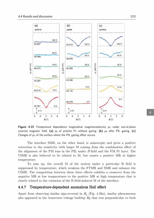
4.4Resultsanddiscussion 123
4
Figure 4.22 Temperature dependence longitudinal magnetoresistivity ρP under out-of-plane external magnetic field. (a) ρP of pristine Pt without gating. (b) ρP after PIL gating. (c) Changes of ρP of the surface where the PIL gating effect occurs.
The interface SMR, on the other hand, is anisotropic and gives a positive correction to the resistivity with larger M coming from the combination effect of the alignment of the PM ions in the PIL under B field and the FM Pt layer. The UIMR is also believed to be related to M, but causes a positive MR at higher temperature.
To sum up, the overall M of the system under a particular B field is suppressed by temperature, which weakens the FTMR and SMR and enhance the UIMR. The competition between these three effects exhibits a crossover from the negative MR at low temperatures to the positive MR at high temperature that is closely related to the variation of the B field-induced M of the interface.
4.4.7 Temperature-dependent anomalous Hall effect
Apart from observing similar sign-reversal in Rp (Fig. 4.23a), similar phenomenon also appeared in the transverse voltage buildup RH that was perpendicular to both

124 Chapter4
4
B and I, namely the anomalous Hall effect (AHE). RH displays clear hysteresis loop at 5 K (Fig. 4.23b), indicating the emergence of a ferromagnetic (FM) state, which shows a perpendicular magnetic anisotropy (Section 3.4.2).
The AHE can be described by [47] , (4.41)
where R0 and RA are the ordinary and anomalous Hall coefficient, respectively. For the whole temperature range from 5 K to 120 K, the hysteresis diminished rapidly, and the sign of the second term in Eq. 4.41 changed at ~60 K (Fig. 4.22), which can be caused by either RA or M.
The theory of AHE sign-reversal is profound despite that it has been observed in many materials experimentally [48-50]. In the present system, since the ordinal Hall effect remains electron-like, the sign reversal of the AHE cannot be ascribed to the global change of the Fermi surface topology.
Skew scattering [51] and side jump [52] are two mechanisms proposed to explain AHE. The former one dominates in the good-metal regime with low resistivity (< 1 μΩ cm) [53], while the later one is sensitive to the impurity type and concentration. In contrast, we obtained ρL as high as 102 μΩ cm, which excludes skew scattering as the origin accounting for AHE sign reversal [53].
Figure 4.23 Temperature-dependent longitudinal magnetoresistance Rp (a) and transverse Hall resistance RH (b) with out-of-plane B field. It is worth noting that RH shows the emergence of anomalous Hall effect and hysteresis loop at 5 K, indicating the existence of ferromagnetic state.

4.4Resultsanddiscussion 125
4
Furthermore, in our experiment, we use the same PIL with Fe3+ as spin dopants and control the concentration by gating to roughly the same voltage when Rs saturates [54]. The sign of AHE reverses only at Pt films above certain thicknesses, which is difficult to reconcile with the side-jump mechanisms. It is worth noting that the AHE sign-reversal temperature is close to those found in longitudinal transport δρL and δρp, implying a common physics background.
4.4.8 Magnetic phase diagram
We summarized all transport results of the PIL-gated Pt system in a magnetic phase diagram shown in Figure 4.24. For thinner films with t = 8 nm and t = 12 nm, δρH remains positive for all the measured temperature range. Because we found that PIL-gated Pt shows FM state at low temperature (in chapter 2), the saturation magnetization was determined by extrapolating the linear part of ρxy at large B field (ρ0 in Eq. 4.41) and fitted the high temperature data (T ≥ 40 K) with the Bloch equation [55]:
1 , (4.42) where δρH
0 is the spontaneous magnetization at T = 0 K and β, the Bloch constant, equals 3/2 for three-dimensional (3D) system.
Figure 4.24 Phase diagram of the PIL-gated Pt films. The red squares, green triangles, blue triangles and purple diamonds denote the in-plane longitudinal (δρL), transverse magnetoresistivity (δρT), and perpendicular magnetoresistivity (δρP) and Hall resistivity (δρH) of 16 nm Pt film, respectively, where δρi = ρi(6T) – ρi(0T). The orange circles and brown hexagons represent the Hall resistivities of 8 nm and 12 nm Pt samples. A sign reversal was observed in 16 nm sample for δρL, δρp and δρH at roughly 40 K, while the sign of δρT remains the same. In thinner samples, a prominent up-turn feature was observed at low temperature. This deviation from the Bloch law suggests the onset of a paramagnetic contribution to the overall magnetization.

126 Chapter4
4
Interestingly, the observed ρH deviates from T3/2 dependence at low temperature. Instead, it increases with 1/T, which belongs to the Curie law for paramagnetism. This low temperature anomaly suggests that the PM contribution of the PIL becomes comparably large at low temperature on top of the FM interaction revealed by AHE. In addition, the temperature dependence of ρH reveals the nature of the paramagnetism correlated MR from another point of view.
For thicker sample (t = 16 nm), besides the low temperature Curie type of up-turn feature, we observed the reversal behavior of the magnetoresistivity sign. For the longitudinal transport with B I, both in-plane (δρL) and out-of-plane (δρP) geometry shows a similar sign-reversal temperature ~40 K, while the transverse behavior is more complicated. In contrast to thinner films, the sign of AHE (δρH) reverses at ~60 K and magnitude continues to grow with increasing temperature.
In addition, in terms of the in-plane transverse magnetoresistivity (δρT), both sign and magnitude hold for all the measured temperature range. This inconsistency implies there might be two mechanisms affecting the transverse transport [56]. We tentatively assign the AHE to the FM contribution of FM Pt layer and the low temperature PHE-like MR to the PM contribution of PIL.
4.4.9 Theory of spin-dependent magnetoresistance at Pt/paramagnetic insulator interface
Because of the highly insulating nature of the PIL that no electrical current can pass through (IG < 10-12 A at 5 K), resistivity mixing of PIL contribution is safely excluded. In addition, the formation of electric double layer under bias VG generates an extremely large electric potential (E = V/d) due to the very short capacitive distance, which is equal to the radius of PIL ions. The electric field attenuates rapidly with deep into the bulk of the channel, limiting the gating effect to the top-most layer of the Pt [57, 58]. Together with strong screening, paramagnetic ionic gating forms an interface with property distinct from the rest of the Pt. We have discussed this induced interface ferromagnetism with perpendicular magnetic anisotropy in chapter 3.
Moreover, since Pt is a heavy metal with strong spin-orbit interaction, large spin Hall effect (SHE) is expected that converts electrical current I to a spin current Is, leading to a spin accumulation μs towards the Pt/PIL interface with its direction normal to both I and Is. Depending on the magnetization direction, μs will be absorbed by the magnetization forming spin-transfer torque; or reflected back to the Pt channel. Because of the inverse spin Hall effect (ISHE), these reflected spins will convert into an electrical current again. Therefore, we attempt to interpret the observed phenomenon by the well-established spin-Hall magnetoresistance (SMR) theory with intrinsic perpendicular magnetization [29, 39].
In Figure 4.25b, when B = 0 T, the direction of M at the FM Pt top-layer is out-of-plane and normal to the spin polarization σ direction of Is coming from bulk

4.4Resultsanddiscussion 127
4
PM Pt. The absorption of μs by M is therefore the strongest, leading to the high resistance state of ρL. Increasing B field gradually pulls down M to the in-plane direction. At ϕ = 0°, σ keeps normal to M, so that the absorption of μ by M remains constant, keeping ρL at high resistance state (Fig. 4.25c).
At ϕ = 90°, however, the angle between M and σ changes from 90° to 0° with increasing B. This will drive the influence of M on μ from maximum absorption to effective reflection, resulting in the decrease of the ρL (Fig. 4.25d). We expect the hybridization of the magnetization from the PIL molecules and the FM Pt top-layer, which forms localized spin-ordered states at the Pt/PIL interface [9, 59-61]. Therefore, with further increase of B field after magnetic moments of FM Pt have been fully aligned, ρL continues to grow because of the PM contribution of PIL.
In contrast, for systems with spontaneous in-plane M, such as Pt/yttrium iron garnet (YIG) bilayer structure, decreasing B to the amount that cannot hold the direction of M will trigger the in-plane precession with a finite remanence through all angle ϕ, which results in ρL changing from the maximum to the minimum and back (Fig. S4.3c) [62]. In addition, due to the finite coercivity of YIG, ρL becomes constant after M is fully aligned to the direction of B, which is significantly different from the non-saturating PM feature of PIL.
Figure 4.25 Theory of the spin-Hall magnetoresistance at Pt/PIL interface with paramagnetic ionic gating. (a) Without PIL gating, Pt shows no resistivity modulation with respect to in-plane B field. (b) After gated with PIL, surface Pt becomes ferromagnetic with perpendicular anisotropy. With applying an in-plane B field, the system is in high (c) and low (d) resistance state with respect to ϕ = 0° and ϕ = 90°, respectively.

128 Chapter4
4
4.5 Supplementary Information
4.5.1 Two-channel model of electrical transport with out-of-plane geometry
The short Thomas-Fermi screening length due to the intrinsically large carrier density in Pt limits the gating effect on to the top-most atomic layer [63], which leaves the bulk remain pristine.
In chapter 3, we discussed the coexistence of the Kondo effect in the presence of the ferromagnetism with the two-channel model. In this chapter, we observed the sign reversal signature of the Hall coefficient at ~60 K. However, the apparent longitudinal transport shows no sign reversal, presumably because of the mixing of the bulk-conducting channel. To find out the correlation between the transverse Hall signal and the surface contribution of the longitudinal magnetoresistance, we apply the two-channel model to separate the surface contribution from the overall experimental results.
Consider a two-channel in parallel model consisting of a surface gated layer that is more conducting and a bulk non-gated layer that has the normal resistance, we have
1 1 1
. (4.43)
Take ρ = Rt into equation (14), we have
, (4.44)
where ts, tb are the effective thickness of the surface gated Pt layer and the bulk non-gated layer, respectively. ρs, ρb and ρ are the surface, bulk and overall resistivities of the channels while ρb and ρ are obtained from the measurements without (Fig. 4.22a) and with PIL gating (Fig. 4.22b), respectively. Eq. 4.44 can be further converted to
. (4.45)
We investigate δρp = ρs(6T) – ρs(0T) and plot the evolution of δρp with temperature T in Figure S4.1. The temperature dependent ρs(0T) can be drawn from analyzing the data from Figure 4.22 into Eq. 4.45. By plotting ρs(0T) versus T, we are able to reconstruct the temperature dependence of sheet resistivity curve of Figure 4.11.

4.5Supplementaryinformation 129
4
Figure S4.1 Simulation of the sign reversal of the longitudinal magnetoresistivity δρp, given by δρp = ρs(6T) – ρs(0T). The legend represents the nominal surface thickness (ts) of the effective gated Pt layer. It is clearly seen that the sign of δρp changes at 25 K, which is close to the experimental value 30 K.
Figure S4.2 Simulated temperature dependent resistivity curves for various surface layer thicknesses (labeled on the right). The black one indicates the R-T curve of pristine non-gated Pt film, which is consistent with Figure 4.11. The blue one with a resistivity change of ~4% is correlated with the gating effect observed in transfer curve (Fig. 4.7) and the R-T curve of gated Pt film (Fig. 4.11).
In Figure S4.2, the nominal thickness of the surface gated layer ts is labeled on the right of the figure. The black line is identical to the green line in Figure 4.11, which refers to the non-gated state. ρs(0T) decreases with increasing gate voltage VG (Fig. S4.2). It is experimentally difficult to determine precisely the effective thickness of the gated layer. However, it is clearly that the thinner the sample is,

130 Chapter4
4
the larger the gating effect, which is reflected as a greater decrease of the sheet resistance Rs (Fig. 4.7).
4.5.2 Comparison of the in-plane magnetoresistance of PIL gated Pt with other systems
In our case of applying an in-plane B field to a material with spontaneous out-of-plane M, sweeping B in principle only affects the in-plane component of M, so that the time reversal symmetry (TRS) will be preserved, where the profile of FDMR is symmetric with B = 0 T (Fig. S4.3a, d).
To demonstrate the significant difference from the AMR of ferromagnet, we fabricated Co thin film sample with thickness of 10 nm that is covered by Al2O3 capping layer to prevent Co from oxidization. The results of magnetoresistance measurement with in-plane B field are shown in Figure S4.3b, d. A prominent ρL drop at low field was observed for B || I, while ρL increase for B I. At ϕ = 45° or 135°, ρL has no change at low field. For the transverse transport measurement, from Eq. 4.7 and Eq. 4.8, we know that the changes of ρT is shifted by 45° from ρL. At ϕ = 45° or 135°, ρT increases and decreases with increase of B, while at ϕ = 0°, 90°, 180°, ρT shows no significant change at low temperature. All data has the same value at B = 0 T.
For the standard SMR system with an in-plane magnetization, such as Pt/YIG, the magnetization direction of the ferromagnetic insulator can be probed with electrical means, referred as the magnitude of the resistance of the proximate Pt layer (Fig. S4.3c, f). For each measurement, we first applied a B field as large as saturating the magnetization of YIG. At ϕ = 0° or 180°, with decreasing B field and eventually reversing the direction of B field, ρL first decreases and then increases at low B field range. At ϕ = 45° or 135°, the behavior of ρL is more complicated. ρL changes first to the lowest value and then increases to the highest value. The observed feature may come from the subtle domain structure, which is interpreted as the in-plane procession of the YIG magnetization that experiences all angle ϕ between B and I, resulting in the full-scale change of ρL. Similar to the AMR of Co, ρT shifts 45° from ρL. Nevertheless, despite the subtle details at low field, the sign of the resistivity changes with respect to ϕ is consistent in both AMR and SMR mechanisms, while in different from the reported PIL-gated Pt system.
In contrast to AMR or conventional SMR, the present non-saturating MR shows a difference in ϕ dependent symmetry. The formers show 4 symmetries for both ρL and ρT, where ρL(ϕ) = –ρL(ϕ+90°) and ρT(ϕ) = –ρT(ϕ+90°); while the later has a 2-fold symmetry for ρL but a 4 symmetry for ρT, where ρL(ϕ) = –ρL(ϕ+180°) and ρT(ϕ) = –ρT(ϕ+90°).

4.5Supplementaryinformation 131
4
Figure S4.3 Comparison of the in-plane magnetoresistance of PIL gated Pt with other systems. (a), (b), (c) Longitudinal magnetoresistivities of Pt/PIL, cobalt thin film and Pt/YIG systems. (d), (e), (f) Transverse magnetoresistivities of Pt/PIL, cobalt thin film and Pt/YIG systems.
At small B field, there is TRS breaking for AMR or SMR due to the M switching or precession. However, as mentioned before, TRS is protected in the presented system, which leads to the magnitude of ∆ρT in FDMR half of the amplitude of ∆ρT in ADMR.
On the other hand, the TRS will be broken with sweeping B perpendicular to the sample xy plane (Fig. 4.23). Magnetization reversal process with finite coercivity can be illustrated by AHE with hysteresis of Hall resistivity ρH at ϕ = 90°, where ϕ is the angle between the B and film xy plane.
4.5.3 Finite element modeling of the electrical transport
At low temperature, where the positive shift of ADMR modulation due to UPMR is minimized, the system can be simply described by the SMR theory with the PMA. In order to confirm the validity, we carried out finite element model calculations to identify the ratio of Rxx/Rxy based on the sample geometry measured from by atomic force microscopy (AFM) (Fig. 4.4). Ideally, the ratio between ∆Rxx and ∆Rxy is given by the ratio between the separation of two Hall-bar electrodes (l) and the width of the Pt channel (w), assuming that the width of the Hall-bar (wbar) leads are negligibly small. Experimentally, however, the Hall leads are often of certain finite widths. In this case, the exact ratio ∆Rxx/∆Rxy may not equal to the dimension of the channel l/w. whereas finite widths (wbar) of the Hall electrodes will cause deviations. For ρxx = ρxy, where
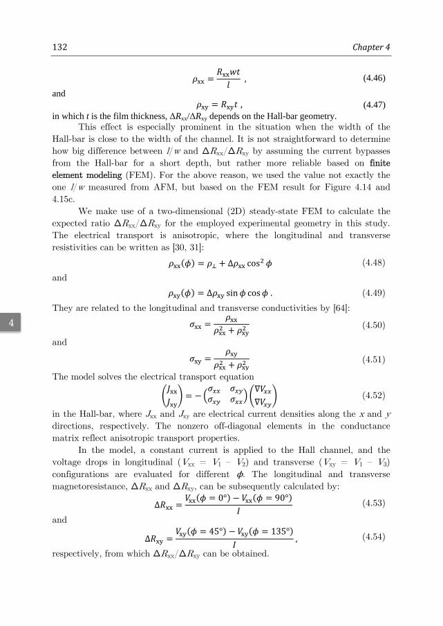
132 Chapter4
4
, (4.46)
and , (4.47)
in which t is the film thickness, ΔRxx/ΔRxy depends on the Hall-bar geometry. This effect is especially prominent in the situation when the width of the
Hall-bar is close to the width of the channel. It is not straightforward to determine how big difference between l/w and ∆Rxx/∆Rxy by assuming the current bypasses from the Hall-bar for a short depth, but rather more reliable based on finite element modeling (FEM). For the above reason, we used the value not exactly the one l/w measured from AFM, but based on the FEM result for Figure 4.14 and 4.15c.
We make use of a two-dimensional (2D) steady-state FEM to calculate the expected ratio ∆Rxx/∆Rxy for the employed experimental geometry in this study. The electrical transport is anisotropic, where the longitudinal and transverse resistivities can be written as [30, 31]:
∆ cos (4.48)
and
∆ sin cos . (4.49)
They are related to the longitudinal and transverse conductivities by [64]:
(4.50)
and
(4.51)
The model solves the electrical transport equation
(4.52)
in the Hall-bar, where Jxx and Jxy are electrical current densities along the x and y directions, respectively. The nonzero off-diagonal elements in the conductance matrix reflect anisotropic transport properties.
In the model, a constant current is applied to the Hall channel, and the voltage drops in longitudinal (Vxx = V1 – V2) and transverse (Vxy = V1 – V3) configurations are evaluated for different ϕ. The longitudinal and transverse magnetoresistance, ∆Rxx and ∆Rxy, can be subsequently calculated by:
∆0° 90°
(4.53)
and
∆45° 135°
, (4.54)
respectively, from which ∆Rxx/∆Rxy can be obtained.

4.5Supplementaryinformation 133
4
Figure S4.4 Finite element model results for anisotropic electrical transport in a Hall-bar geometry. (a) The 2D Hall bar geometry used in this study. Color represents the voltage profile when sourcing a current through the Hall bar. Voltages are probed through V1, V2 and V3 terminals. (b) The ratio ∆Rxx/∆Rxy calculated as a function of the width of Hall-bar (wbar).
Therefore, increasing the width of the Hall-bar will decrease the ratio ∆Rxx/∆Rxy. The reason that we designed a relatively wide Hall-bar was because it was more robust and made the device less likely to be burnt during measurements.
On the other hand, even though at 5 K ∆ xx/∆ xy ≈ 1 indicates the resistivity modulation is of the same origin for both longitudinal and transverse transports, the temperature-dependent sign reversal happens for xx, not xy implies that the observed phenomena have more mechanism working simultaneous rather than a simple AMR type of behavior.

134 Chapter4
4
4.6 Summary To sum up, magnetoresistive devices in general require the usage of ferromagnets, where the magnetization direction is crucial to the electrical transport. Paramagnets have often been regarded less interesting to new MR effect for lacking spontaneous magnetization and long range magnetic ordering. On the other hand, it is highly desirable to control the magnetization electrically from both fundamental and technological points of view. Due to intrinsically large carrier densities and consequently short Thomas-Fermi screening lengths, metals are difficult to manipulate electrically by gating.
Ionic gating, however, offers a unique approach that is able to alter the electronic state of the channel surface significantly by applying only a few volts. Our reported paramagnetic ionic gating technique combines the advantage of ionic gating with magnetic moments, which imparts a new degree of freedom to the controllable transport properties of electron: the spin.
In this chapter, we report the observation of a new type of MR in the non-magnetic metal (NM)/paramagnetic insulator (PMI) system by an in-plane B field. The magnitude of this new MR is proportional to the magnetization built-up of the proximate paramagnetic insulator under B. Contrary to the AMR of ferromagnets that saturates after magnetization are fully aligned, the observed MR can be well described with Langevin function of paramagnetism, which gives rise to the non-saturating contribution to both the longitudinal and transverse MR.
Our experiment extends the concept and application of the SMR mechanism in a Pt/paramagnet insulator system with spontaneous perpendicular magnetization. The observed Langevin type of MR serves as an evidence of paramagnetism induced electrical transport. The emergent phenomena are gate tunable, which paves the path of developing new type of spintronic devices.

4.7References 135
4
4.7 References [1] Bogani L, Wernsdorfer W, "Molecular spintronics using single-molecule
magnets", Nat Mater 7, 179-86 (2008). [2] Mossin S, Tran BL, Adhikari D, Pink M, Heinemann FW, Sutter J, Szilagyi
RK, Meyer K, Mindiola DJ, "A mononuclear Fe(III) single molecule magnet with a 3/2↔5/2 spin crossover", J Am Chem Soc 134, 13651-61 (2012).
[3] Mannini M, Pineider F, Sainctavit P, Danieli C, Otero E, Sciancalepore C, Talarico AM, Arrio M-A, Cornia A, Gatteschi D, Sessoli R, "Magnetic memory of a single-molecule quantum magnet wired to a gold surface", Nat Mater 8, 194-7 (2009).
[4] Herrmann C, Solomon GC, Ratner MA, "Organic Radicals As Spin Filters", J Am Chem Soc 132, 3682-4 (2010).
[5] Coronado E, Martí Gastaldo C, Navarro-Moratalla E, Burzurí E, Camón A, Luis F, "Hybrid magnetic/superconducting materials obtained by insertion of a single‐molecule magnet into TaS2 layers", Adv Mater 23, 5021-6 (2011).
[6] Porath D, Bezryadin A, de Vries S, Dekker C, "Direct measurement of electrical transport through DNA molecules", Nature 403, 635-8 (2000).
[7] Komeda T, Isshiki H, Liu J, Zhang Y-F, Lorente N, Katoh K, Breedlove BK, Yamashita M, "Observation and electric current control of a local spin in a single-molecule magnet", Nat Commun 2, 217 (2011).
[8] Xiong ZH, Wu D, Vardeny ZV, Shi J, "Giant magnetoresistance in organic spin-valves", Nature 427, 821-4 (2004).
[9] Raman KV, Kamerbeek AM, Mukherjee A, Atodiresei N, Sen TK, Lazić P, Caciuc V, Michel R, Stalke D, Mandal SK, Blügel S, Münzenberg M, Moodera JS, "Interface-engineered templates for molecular spin memory devices", Nature 493, 509-13 (2013).
[10] Ye JT, Zhang YJ, Akashi R, Bahramy MS, Arita R, Iwasa Y, "Superconducting dome in a gate-tuned band insulator", Science 338, 1193-6 (2012).
[11] Baibich MN, Broto JM, Fert A, Van Dau FN, Petroff F, Etienne P, Creuzet G, Friederich A, Chazelas J, "Giant magnetoresistance of (001)Fe/(001)Cr magnetic superlattices", Phys Rev Lett 61, 2472-5 (1988).
[12] Binasch G, Grünberg P, Saurenbach F, Zinn W, "Enhanced magnetoresistance in layered magnetic structures with antiferromagnetic interlayer exchange", Phys Rev B 39, 4828 (1989).
[13] Pannetier M, Fermon C, Le Goff G, Simola J, Kerr E, "Femtotesla magnetic field measurement with magnetoresistive sensors", Science 304, 1648-50 (2004).
[14] Dery H, Dalal P, Cywiński Ł, Sham LJ, "Spin-based logic in semiconductors for reconfigurable large-scale circuits", Nature 447, 573-6 (2007).

136 Chapter4
4
[15] Ohno H, Chiba D, Matsukura F, Omiya T, Abe E, Dietl T, "Electric-field control of ferromagnetism", Nature 408, 944 (2000).
[16] Chiba D, "Electrical Manipulation of Magnetization Reversal in a Ferromagnetic Semiconductor", Science 301, 943-5 (2003).
[17] Yamanouchi M, Chiba D, Matsukura F, Ohno H, "Current-induced domain-wall switching in a ferromagnetic semiconductor structure", Nature 428, 539-42 (2004).
[18] Hirai T, Koyama T, Obinata A, Hibino Y, Miwa K, Ono S, Kohda M, Chiba D, "Control of magnetic anisotropy in Pt/Co system using ionic liquid gating", Appl Phys Express 9, 063007-5 (2016).
[19] Shimamura K, Chiba D, Ono S, Fukami S, Ishiwata N, Kawaguchi M, Kobayashi K, Ono T, "Electrical control of Curie temperature in cobalt using an ionic liquid film", Appl Phys Lett 100, 122402 (2012).
[20] Obinata A, Hibino Y, Hayakawa D, Koyama T, Miwa K, Ono S, Chiba D, "Electric-field control of magnetic moment in Pd", Sci Rep 5, 14303 (2015).
[21] Potter RI, "Magnetoresistance anisotropy in ferromagnetic NiCu alloys", Phys Rev B 10, 4626 (1974).
[22] Grünberg P, Schreiber R, Pang Y, Brodsky MB, Sowers H, "Layered magnetic structures: evidence for antiferromagnetic coupling of Fe layers across Cr interlayers", Phys Rev Lett 57, 2442-5 (1986).
[23] Tokura Y, Tomioka Y, "Colossal magnetoresistive manganites", J Magn Magn Mater 200, 1-23 (1999).
[24] Xu R, Husmann A, Rosenbaum TF, Saboungi ML, Enderby JE, Littlewood PB, "Large magnetoresistance in non-magnetic silver chalcogenides", Nature 390, 57-60 (1997).
[25] Husmann A, Betts JB, Boebinger GS, Migliori A, Rosenbaum TF, Saboungi ML, "Megagauss sensors", Nature 417, 421-4 (2002).
[26] Parish MM, Littlewood PB, "Non-saturating magnetoresistance in heavily disordered semiconductors", Nature 426, 162-5 (2003).
[27] Ali MN, Xiong J, Flynn S, Tao J, Gibson QD, Schoop LM, Liang T, Haldolaarachchige N, Hirschberger M, Ong NP, Cava RJ, "Large, non-saturating magnetoresistance in WTe2", Nature 514, 205–8 (2014).
[28] Kobs A, Heße S, Kreuzpaintner W, Winkler G, Lott D, Weinberger P, Schreyer A, Oepen HP, "Anisotropic interface magnetoresistance in Pt/Co/Pt sandwiches", Phys Rev Lett 106, 217207 (2011).
[29] Nakayama H, Althammer M, Chen YT, Uchida K, Kajiwara Y, Kikuchi D, Ohtani T, Geprägs S, Opel M, Takahashi S, Gross R, Bauer GEW, Goennenwein STB, Saitoh E, "Spin-Hall magnetoresistance induced by a nonequilibrium proximity effect", Phys Rev Lett 110, 206601 (2013).
[30] McGuire TR, Potter RI, "Anisotropic magnetoresistance in ferromagnetic 3d alloys", IEEE Trans Magn 11, 1018-38 (1975).

4.7References 137
4
[31] Ky VD, "Planar Hall effect in ferromagnetic films", Phys Status Solidi B 26, 565-9 (1968).
[32] Ky VD, "Planar Hall and Nernst effect in ferromagnetic metals", Phys Status Solidi B 22, 729-36 (1967).
[33] Ralph DC, Stiles MD, "Spin transfer torques", J Magn Magn Mater 320, 1190-216 (2008).
[34] Isasa M, Bedoya-Pinto A, Vélez S, Golmar F, Sánchez F, Hueso LE, Fontcuberta J, Casanova F, "Spin Hall magnetoresistance at Pt/CoFe2O4 interfaces and texture effects", Appl Phys Lett 105, 142402 (2014).
[35] Aqeel A, Vlietstra N, Heuver JA, Bauer GEW, Noheda B, van Wees BJ, Palstra TTM, "Spin-Hall magnetoresistance and spin Seebeck effect in spin-spiral and paramagnetic phases of multiferroic CoCr2O4films", Phys Rev B 92, 224410 (2015).
[36] Ding Z, Chen BL, Liang JH, Zhu J, Li JX, Wu YZ, "Spin Hall magnetoresistance in Pt/Fe3O4 thin films at room temperature", Phys Rev B 90, 134424-4 (2014).
[37] Kim J, Sheng P, Takahashi S, Mitani S, Hayashi M, "Spin Hall magnetoresistance in metallic bilayers", Phys Rev Lett 116, 097201-5 (2016).
[38] Shang T, Zhan QF, Ma L, Yang HL, Zuo ZH, Xie YL, Li HH, Liu LP, Wang BM, Wu YH, Zhang S, Li R-W, "Pure spin-Hall magnetoresistance in Rh/Y3Fe5O12 hybrid", Sci Rep 5, 17734 (2015).
[39] Chen Y-T, Takahashi S, Nakayama H, Althammer M, Goennenwein STB, Saitoh E, Bauer GEW, "Theory of spin Hall magnetoresistance", Phys Rev B 87, 144411 (2013).
[40] Blundell S, "Magnetism in condensed matter", Oxford University Press Inc., New York (2001)
[41] de Pedro I, Rojas DP, Albo J, Luis P, Irabien A, Blanco JA, Rodríguez Fernández J, "Long-range magnetic ordering in magnetic ionic liquid: Emim[FeCl4]", J Phys: Condens Matter 22, 296006 (2010).
[42] Joseph A, Żyła G, Thomas VI, Nair PR, Padmanabhan AS, Mathew S, "Paramagnetic ionic liquids for advanced applications: A review", J Mol Liq 218, 319-31 (2016).
[43] Milner A, Gerber A, Groisman B, Karpovsky M, Gladkikh A, "Spin-dependent electronic transport in granular ferromagnets", Phys Rev Lett 76, 475-8 (1996).
[44] Gerber A, Milner A, Groisman B, Karpovsky M, "Magnetoresistance of granular ferromagnets", Phys Rev B 55, 6446-52 (1997).
[45] Sacharoff AC, Westervelt RM, Bevk J, "Magnetoresistance of disordered ultrathin Pt wires", Phys Rev B 29, 1647-52 (1984).
[46] Mott NF, "The electrical conductivity of transition metals", Proc R Soc A 153, 699 (1936).

138 Chapter4
4
[47] Pugh EM, Rostoker N, "Hall effect in ferromagnetic materials", Rev Mod Phys 25, 151 (1953).
[48] Coles BR, Taylor JC, "Sign reversal of the Hall effect in Rhodium", J Phys Chem Solids 1, 270-4 (1957).
[49] Lindqvist P, Berger C, Klein T, Lanco P, Cyrot-Lackmann F, Calvayrac Y, "Role of Fe and sign reversal of the Hall coefficient in quasicrystalline Al-Cu-Fe", Phys Rev B 48, 630-3 (1993).
[50] Gausepohl SC, Lee M, Rao RA, Eom CB, "Hall-effect sign reversal in CaRuO3 and SrRuO3 thin films", Phys Rev B 54, 8996-9 (1996).
[51] Smit J, "The spontaneous Hall effect in ferromagnetics I", Physica 21, 877-87 (1955).
[52] Berger L, "Side-jump mechanism for the Hall effect of ferromagnets", Phys Rev B 2, 4559-66 (1970).
[53] Nagaosa N, Sinova J, Onoda S, MacDonald AH, Ong NP, "Anomalous Hall effect", Rev Mod Phys 82, 1539-92 (2010).
[54] Su YZ, Fu YC, Yan JW, Chen ZB, Mao BW, "Double layer of Au(100)/ionic liquid interface and its stability in imidazolium‐based ionic liquids", Angew Chem 121, 5250-3 (2009).
[55] Klein MJ, Smith RS, "Thin ferromagnetic films", Phys Rev 81, 378 (1951). [56] Shimizu S, Takahashi KS, Hatano T, Kawasaki M, Tokura Y, Iwasa Y,
"Electrically tunable anomalous Hall effect in Pt thin films", Phys Rev Lett 111, 216803 (2013).
[57] Ye JT, Inoue S, Kobayashi K, Kasahara Y, Yuan HT, Shimotani H, Iwasa Y, "Liquid-gated interface superconductivity on an atomically flat film", Nat Mater 9, 125-8 (2009).
[58] Lu JM, Zheliuk O, Leermakers I, Zeitler U, Yuan N, Ye JT, "Evidence for two-dimensional Ising superconductivity in gated MoS2", Science 350, 1353 (2015).
[59] Bernien M, Miguel J, Weis C, Ali ME, Kurde J, Krumme B, Panchmatia PM, Sanyal B, Piantek M, Srivastava P, Baberschke K, Oppeneer PM, Eriksson O, Kuch W, Wende H, "Tailoring the nature of magnetic coupling of Fe-porphyrin molecules to ferromagnetic substrates", Phys Rev Lett 102, 047202 (2009).
[60] Zhang X, Mizukami S, Kubota T, Oogane M, Naganuma H, Ando Y, Miyazaki T, "Interface effects on perpendicular magnetic anisotropy for molecular-capped cobalt ultrathin films", Appl Phys Lett 99, 162509-4 (2011).
[61] Ma’Mari FA, Moorsom T, Teobaldi G, Deacon W, Prokscha T, Luetkens H, Lee S, Sterbinsky GE, Arena DA, MacLaren DA, Flokstra M, Ali M, Wheeler MC, Burnell G, Hickey BJ, Cespedes O, "Beating the Stoner criterion using molecular interfaces", Nature 524, 69-73 (2015).
[62] Vlietstra N, Shan J, Castel V, van Wees BJ, Ben Youssef J, "Spin-Hall magnetoresistance in platinum on yttrium iron garnet: Dependence on

4.7References 139
4
platinum thickness and in-plane/out-of-plane magnetization", Phys Rev B 87, 184421 (2013).
[63] Comtet J, Nigu s A, Kaiser V, Coasne B, Bocquet Lr, Siria A, "Nanoscale capillary freezing of ionic liquids confined between metallic interfaces and the role of electronic screening", Nat Mater 16, 634-9 (2017).
[64] Singleton J, "Band Theory and Electronic Properties of Solids", Oxford University Press Inc., New York (2001)


In preparation: Lei Liang, Qihong Chen, Graeme R. Blake, Thomas T. M. Palstra, Jianting Ye– “Giant magnetic anisotropy in layered manganese intercalated tantalum disulfide thin flake”
Chapter 5
Giant Magnetic Anisotropy in Layered Manganese Intercalated Tantalum Disulfide Thin Flake
agnetic anisotropy is an intrinsic property of magnetic
materials. The magnetization of a ferromagnet tends to
align with certain preferential direction. Magnetic ion
intercalated transition metal dichalcogenide is a family of
layered materials that exhibits extremely large magnetic
anisotropy. Depending on the element of intercalants, the
resulting magnetic anisotropy can favor either the direction
perpendicular to the lattice plane or within the lattice plane.
In this chapter, we will focus on the magnetic measurement of
the Mn intercalated tantalum disulfide with a stoichiometric
ratio of Mn1/4TaS2. This material shows a giant magnetic
anisotropy with an easy plane.
M

142 Chapter5
5
5.1 Introduction
5.1.1 Layered materials
Since the discovery of new physics on graphene and topological insulators, systems with hexagonal layers bound by van der Waals bonding have been refocused in the condensed matter physics society. Among them, the most well-known members are Xenes, carbides, nitrides, oxides, halides and transitional metal dichalcogenide.
Xenes refers to the monolayer of IVA group elements. The most famous one is the monolayer carbon, namely graphene. Ultrahigh mobility was achieved in graphene field-effect transistors (FET), which is of promise to be a good candidate of the next generation electronics [1]. Ever since that, monolayers of other elements in the IVA group have been discovered. A Silicene FET was prepared by depositing on Ag (111) film on mica substrate. Later the film was detached and flipped back to the top of SiO2/Si wafer [2]. Germanene film was grown via molecular beam epitaxy on gold surface and then mechanically exfoliated [3]. Single layer of tin (stanene) was grown by molecular beam epitaxial (MBE) on Bi2Te3 (111) substrate [4]. Monolayer lead film was also been reported and the superconducting gap was measured [5].
One large group of the layered carbide (nitride) is called MAXene. It refers to a ternary system with a combination of transitional metal element (M), carbon or nitrogen (X) and a third element (A) in some specific compositions (M2AX, M3AX2, M4AX3). It is useful in terms of energy storage [6]. The most widely used nitride is the hexagonal boron nitride (h-BN). Because of its highly insulating nature and easily cleavable characteristic, it has been used as insulating layer for fabricating nano-heterostructure [7, 8],
Layered oxides have been studied for decades in terms of their importance in energy storage. Lithium cobalt oxide is probably the material that is relevant to everyone because it is the cathode material for the battery inside our mobile phone and other portable devices [9]. In addition, hydrated sodium intercalated cobalt oxide is found to be superconducting [10].
Halogen elements can bond with oxygen or nitrogen atom and form covalent compound with transition metal elements, namely oxychloride and chlorine nitride. Intercalating alkali metal or applying ionic liquid gating can tune these materials into superconducting [11, 12]. Halogen elements can also form ionic compound directly with transition metal elements. For example, CrI3 is a layered ferromagnetic insulator and when it is down to the monolayer limit, itinerant ferromagnetism emerges for monolayer while the magnetization is suppressed for bilayer film [13, 14].

5.1Introduction 143
5
Figure 5.1 Summary of layered materials. Different colors illustrate different material groups and are labelled with corresponding color in the legend.
Recently, transitional metal dichalcogenide (TMD) attracts growing interests for their fascinating properties. TMD refers to a large family of compounds with formula MX2, where M is transition metal atom (Mo, W, Ta, Nb, etc.) and X is chalcogen atom (S, Se or Te). Because of the large variation of the element selection, the electronic properties can vary from semiconducting (e.g. MoS2 [15]), to semi-metal (e.g. WTe2 [16]) till metallic (e.g. NbSe2 [17]). They are also interesting in terms of optical properties. Because of the peculiar band structure that two minima at equal energies but different in momentum positions, different polarization will excite different valleys [18, 19].
Besides TMD, chalcogen elements also participate in forming topological insulators (M2X3) and thiophosphate (MPS3). The former one has been widely studied since the emergence of the Dirac materials [20, 21] and the later one starts to be restudied for its interesting magnetic properties [22].
The quest of novel physics and promising application in “ultimate flatland” [23] has just started. Many more layered materials are ready to be discovered and new physical properties are also expected.

144 Chapter5
5
5.1.2 Transition metal dichalcogenide
The study of TMDs has been carried on for decades. A wide range of interesting electronic, optical and mechanical properties has been discovered by researchers [24-26]. The isolation of monolayer graphene from bulk graphite [27] has opened up new opportunities for applications of atomically thin two dimensional (2D) materials. Although graphene has ultrahigh mobility up to 106 cm-2 V-1 s-1, the linear dispersion relation near the Dirac point limits it as a semimetal with zero band gap. Therefore, the field effect transistor made by graphene has a very low on/off ratio. New materials with high mobility and energy gap are eager to be discovered. The large variety of TMD makes it a very interesting candidate.
Bulk TMDs, like graphite, can be regarded as stacking of monolayers with van der Waals attraction. It has been proved that they can be easily exfoliated into individual atomically thin layers due to weak interlayer coupling. As analogue of graphene, many monolayer TMDs have moderate band gaps of 1 to 2 eV, where the carrier density can be effectively tuned by the field effect [28, 29]. Monolayer TMDs can be directly grown by chemical vapor deposition method.
The structures of TMDs are shown in Figure 5.2. Each plane of transition metal atoms is sandwiched between two chalcogen atom planes (Fig. 5.2a), forming a hexagonal structure (Fig. 5.2b). Two type of polyhedrons are formed, which are hexagonal and trigonal prismatic coordination, respectively (Fig. 5.2c,d).
Depending on the stacking orders and metal atom coordination, TMD has three different polytypes: 1T, 2H and 3R as shown in Figure 5.3a. The repeating unit of each polytypes is one, two and three layers, respectively. The stacking geometry is better illustrated from the top view (Fig. 5.3b). The lattice constants are in the range of 3.1 to 3.7 Å for different materials and the interlayer spacing is around 6.5 Å. Because of its weak interlayer coupling, other intercalants can be inserted in between the layers. In this chapter, we will study the magnetism of manganese intercalated TaS2 thin flake.
Figure 5.2 (a) Side view of TMD layered structure (2-H), each transition metal layer (blue sphere) is sandwiched between two chalcogen layers (green sphere)

5.1Introduction 145
5
Figure 5.3 (a) Schematic diagrams of three structural polytypes: 1T (tetragonal symmetry), same layer (in grey) repeats each other, M-X forms octahedral coordination; 2H (hexagonal symmetry) two unit layers (in grey and yellow) repeat one another, M-X forms trigonal prismatic coordination; 3R (rhombohedral symmetry), three different layers (in grey, yellow and cyan) repeat one another, M-X forms trigonal prismatic coordination. (b) Top views of layered TMD structure in one unit cell. For each repeating layer, one M plane (in big blue sphere) is sandwiched between two X planes (in small green sphere).
5.1.3 Types of magnetic anisotropy
There are several origins causing magnetic anisotropy. The first one is due to the crystal structure, hence is named magnetocrystalline anisotropy. If a ferromagnet takes more energy to be magnetized in certain directions, which is of the principal axes of its crystal lattice, then these axes are called hard axes, which means they are hard the be magnetized. At the same time, once they are magnetized, it is also difficult to be demagnetized that results in high coercivity. As a matter of fact, this type of ferromagnets is often be used as permanent magnets in applications, such as magnetic cores for transformers and inductors. To further strengthen the large anisotropy, rare earth elements are used for synthesizing the permanent magnets for the reasons that they possess large magnetic moments and strong spin-orbit interactions (SOC).
The microscopic origin of the magnetocrystalline anisotropy arises from the SOC. Although compared to the exchange interaction that causes the spontaneous

146 Chapter5
5
magnetization, SOC is a relatively weak effect; it does have significant impacts on the determination of magnetization direction. The spin of electrons interacts with the atoms of crystal via SOC, so that different atomic orbitals related to the particular crystal structure lead to different orientation of the spins. As a result, the magnetic moments from the spins are energetically favorable towards some directions: the easy axes.
Magnetic anisotropy is a prerequisite for hysteresis in ferromagnets. For magnetic isotropic materials, there are no preferential directions for the magnetic moment to lie on unless there is external magnetic field to do so, such as paramagnetic materials. If the crystal size is smaller than the magnetic domain, magnetic anisotropy energy (KV) can be relatively smaller than the influence of temperature (kBT). Once the time interval (τN) between two spin flips is shorter than the time of measurement (τm), the magnetization behaves like a paramagnet, and the state is termed superparamagnetism although the magnetic susceptibility is much larger than the paramagnets. On the other hand, if τm ≪ τN, during the measurement, the magnetization will not flip and appear to be blocked in its initial state. The temperature at which τm =τN is called blocking temperature:
ln
(5.1)
where K is the magnetic anisotropy density, V the volume, kB the Boltzmann constant, τ0 the characteristic attempt time period of a material that spin flip takes.
When a ferromagnet is not perfectly spherical, the demagnetizing field that is created by the edge magnetic poles will be not equivalent, resulting in another type of magnetic anisotropy called shape anisotropy. In general, for thin film ferromagnet, the shape anisotropy will lead to an in-plane magnetization.
There is a presence of a symmetry breaking at material surface or interface. Hence, the orbital motion of electrons is affected and creates a surface anisotropy. The surface anisotropy is given by the sum of two terms, namely the surface contribution Ks/t and the volume contribution Kv. If the film is very thin, the surface term dominates. Due to the perpendicular surface anisotropy, all magnetic moments point out of plane, leading to the perpendicular spontaneous magnetization.
Besides magnetic field, other external factor may cause change of magnetic susceptibility, such as mechanical stress. This effect is opposite of the magnetostrictive effect, so that the resulted magnetic anisotropy is called magnetoelastic anisotropy. In ferromagnets, applying a mechanical stress to the body will cause reorientation of the magnetization through magnetostrictive effect. The associated energy is proportional to the magnitude of magnetic moment polarization σ and a material dependent magnetostriction constant λ that represents the maximum response of the strain to the magnetic field, which is described as

5.1Introduction 147
5
32
cos , (5.2)
where θ is the angle between magnetization and the stress direction. The last but not least type of anisotropy occurs in the bilayer interface
between a ferromagnetic and an antiferromagnetic thin film. The antiferromagnetic film is hard to be magnetized, while for the ferromagnetic film is comparably easy. The magnetization curve of the ferromagnetic film will be shifted due to the exchange anisotropy. Microscopically, this is because the spin of the ferromagnet is strongly exchange-coupled to the proximate antiferromagnet. Since the antiferromagnet has little magnetization response to the external magnetic field, the spin in the ferromagnet is pinned to the direction of the spin in the antiferromagnet. Therefore, an extra energy cost is necessary for reversing the magnetization of the ferromagnetic film. The difference (in magnetic field) between the centers of the hysteresis loop for the ferromagnetic film before and after attached to the antiferromagnetic film is called the exchange bias.
5.2 Concepts 5.2.1 Magnetocrystalline anisotropy
Ferromagnets contain magnetic domains that within each small region, the magnetization direction is the same, while may not be identical to other regions. This is why it is only necessary to apply a weak magnetic field to fully magnetize a ferromagnet. In contrast to paramagnets, where magnetic field is for aligning all magnetic moments, the effect of magnetic field on ferromagnets is to rotate the magnetization direction of individual domains.
Between two domains with different magnetization direction, there is a symmetry breaking in the domain wall. Considering two spins at the interface lie at an angle α with respect to each other. This will produce an energy cost (for small α) α . (5.3)
Figure 5.4 The relative directions of the material easy axis with respect to magnetization and external magnetic field. The angles are denoted as ϑ and ϕ,respectively.

148 Chapter5
5
It seems unlikely that domains can exist. However, there is some other interaction that prohibits the spins from aligning to each other, which is called the magnetocrystalline anisotropy.
Originated from the crystal structure, it is in general easy to magnetize the crystal along certain axis that is termed as magnetic easy axis. In case of hexagonal system (Mn1/4TaS2) that is uniaxial with a six-fold rotation symmetry c-axis, the associated anisotropy energy can be written as
sin sin sin ⋯ sin , (5.4)
which the lowest order terms are given by sin sin , (5.5)
where K1, K2, are anisotropy constants and ϑ is the angle between magnetization M and easy axis (Fig. 5.4).
The minima in the energy with respect to ϑ satisfy
0, (5.6)
and
0. (5.7)
Therefore, we could map the phase diagram of the easy magnetized directions as a function of K1 and K2, shown in Figure 5.5.
In addition, the magnetostatic potential energy (Zeeman energy) of a ferromagnet under magnetic field H is given by cos (5.8)
where ϕ is the angle between external magnetic field H and easy axis.
Figure 5.5 Basic phase diagram based on the calculation from K1 and K2 values of an uniaxial ferromagnet.

5.2Concepts 149
5
For a simple single-domain ferromagnet, the energy of the system with respect to an external magnetic field is a sum of these two terms . (5.9)
Substituting Eq. 5.9 by Eq. 5.5 and Eq. 5.8, we have the expression of the energy in the system sin cos . (5.10)
Eq. 5.10 can be normalized to
214
14cos 2
2cos . (5.11)
By defining
2
. (5.12)
Eq. 5.11 can be rewritten to 1
414cos 2 cos . (5.13)
For each ϑ, we can plot the h-dependent of the E as a function of ϕ. The results are summarized in Figure 5.6a. Applying Eq. 5.6 and Eq. 5.7, we can find out the energy minima point. Consequently, we have the corresponding values of (ϕ – ϑ). Then M/Ms can be derived from
cos – . (5.14)
Since h is proportional to external magnetic field H, by plotting M/Ms vs. h, the angle dependence of magnetization is illustrated in Figure. 5.6b.
It is clear to see how hysteresis loop and the coercivity evolve. This model is called the Stoner-Wohlfarth model. It implies that even without domain wall motion, single domain magnet can have hysteresis in the magnetization curve due to domain rotation.
Figure 5.6 Stoner-Wohlfarth model of the numerically simulated ferromagentic magnetization curves. (a) The 3-D wire surface plot of the relations between η, ϕ and h for several characteristic angles between M and H direction. (b) The derived M/Ms vs. h shows hyteresis loops because there are two energy minima at each h (H) value.

150 Chapter5
5
The anisotropy constant is related to three terms: the surface, volume and shape anisotropy: 2
. (5.15)
The surface term is proportional to 1/t, indicating that it can dominate in ultrathin film. The volume term is only obvious in strained or uniaxial single crystals. The shape anisotropy term is from the contribution of the dipolar energy, normally dominating for thick films and leads to the in-plane magnetization. Therefore, the magnetic properties of a monolayer film are expected to be different from the bulk.
From the itinerant ferromagnetism point of view, the atoms at the surface have smaller numbers of nearest neighbors compared with those in bulk. The reduction of the coordination number leads to the narrowing of the bandwidth and increases the density of states at the Fermi level, hence the opportunity that Stoner criterion being satisfied, which enhances the propensity of long range magnetic ordering.
5.2.2 SQUID Magnetometry
Superconducting quantum interference device (SQUID) magnetometry is one of the most effective and sensitive ways of measuring magnetic properties. In particular, it is the only method that allows direct determination of the overall magnetic moment of a sample in absolute units.
Figure 5.7 Systematic diagram of the mechanism that how does the SQUID work. The left panel shows the schematic illustration of the SQUID pick-up coil as well as the sample. The right panel displays the signal corresponding to the movement of the sample straw.

5.2Concepts 151
5
The working mechanism is based on the Josephson effect that was established by Brian David Josephson in 1962, which the electrical current density through a weak electric contact between two superconductors depends on the phase difference ∆φ between two superconducting wave functions. The time derivative of ∆φ is correlated with the voltage across the weak contact.
The magnetic results in this chapter were measured from a commercial SQUID magnetometer system produced by Quantum Design, San Diego. The equipment type is Magnetic Properties Measurement System (MPMS) XL-7. The image and basic sample preparation procedures will be discussed in Appendix. Here, we will focus on the principle of the SQUID.
Figure 5.7 shows the schematic diagram of the working principle of SQUID. The magnetic signal of the sample is obtained via a superconducting pick-up coil with 4 circles (in red). Sample straw was moving up and down along the magnetic field direction alternatively by a step-motor. The changing of the position in turn causes a change of the magnetic flux. A screening current hence generates in the pick-up coil to cancel the external flux. This will transfer the magnetic flux of the sample into a radio frequency voltage signal (in green). With the movement of the sample, the voltage response to the full measurement range can be extracted. Therefore the center of the sample and the amplitude of the magnetic flux can be calculated by fitting the curve (in blue). The core of the SQUID system is the pick-up coil, which is made of some superconducting metals, such as niobium (Nb). In order to maintain the superconductivity, the pick-up coil is located outside of the sample chamber and is placed in the liquid helium bath at constant 4.2 K.
The sample is located in the center of a superconducting solenoid (in different from the pick-up coil) producing magnetic fields up to 7 Tesla. The sample space is filled with helium at low pressure at temperatures ranging from 2 to 400 K. The sensitivity is up to 10-8 emu in reciprocating sample oscillation (RSO) mode, which is equivalent to the saturation magnetization of six billionth mm3 of iron. The whole system is program and can be continuously operated.
5.3 Experiments 5.3.1 Crystal growth
A systematic crystal growth procedure was carried out to obtain large single crystal. First, the stoichiometric Mn1/4TaS2 powder was obtained by heat treatment of Mn, Ta and S powders in an evacuated quartz tube at 900 °C. The tube was open in glove box and the obtained powder was ground in agate mortar. The powder was sealed in quartz tube under vacuum again and heated at 900 °C for another 5 days. As a result, the pure Mn1/4TaS2 powder was synthesized and characterized by powder X-ray diffraction.

152 Chapter5
5
Figure 5.8 Optical microscope image of Mn1/4TaS2 single crystal with various size and thickness. Flat terraces (cleavage surfaces) can be recogenized.
The single crystal Mn1/4TaS2 was grown using chemical vapor transport (CVT) with iodine as transport agent. The ratio between the iodine and the polycrystalline Mn1/4TaS2 powder is 10:1. Same to the synthesis of powder sample, 1 gram of as-prepared powder and 0.1 gram iodine were mixed and sealed in an evacuated quartz tube with a length of ~20 cm. The tube was placed in a two-zone tube furnace with the hot zone at ~1000 °C and the growth zone at ~900 °C. Depending on the growth time, the single crystal shape can vary from large-flat thin flake to small-thick crystals with clear edge and corner. Because MnxTaS2 exists in many phases, in reality, small amounts of impurity phases may exist. So small adjustment of the stoichiometry is necessary, namely 0.25×N (0.96<N<1.15).
5.3.2 X-ray diffraction
In order to confirm the crystallinity of the measured sample, x-ray diffraction experiment was performed. The data were collected using a Bruker D8 advance powder diffractometer. It employs Cu target as anti-cathode.
Figure 5.9 Principle of x-ray diffraction. (a) The diffraction measurement setup. (Bruker©) (b) Multiple reflections of a wave of an angle of incidence that equals the Bragg condition of constructive interference for a set of lattice planes.

5.3Experiments 153
5
The x-ray is generated with the following process. First the K-shell electrons are knocked out with the incident high-energy electron. The maximum accelerating voltage is 40 kV and the electron probe current range is up to 40 mA. The vacancies can be filled by electrons from the L-shell (or M-shell), radiating x-ray with a wavelength of 1.54 Å for the characteristic Kα spectrum. According to the Bragg’s law:
2 sin . (5.16)
where λ is the wavelength of the incident light and θ is the angle between the incident light and the direction normal to sample plane. The lattice distance d can be calculated accordingly (Fig. 5.9).
From the x-ray diffraction spectrum, we can read out the information about the crystal, such as the crystal plane direction. With further refinement, we can even derive the precise lattice parameters and atomic positions. Figure 5.10a shows the full-range XRD spectrum from a single flake of Mn1/4TaS2 sample. The sample was placed on top of a suspended kapton tape in order to minimize the signal background from the substrate. The data was collected with an angle step size of 0.02° from 10° to 90° and interval during time of 0.1 s.
The inset of Figure 5.10a shows the zoom-in of the spectrum at the main peak position θ ≈ 13°. The data was re-collected with an angle step size of 0.001° (highest resolution) from 13.4° to 14.0°. We noticed that there are a number of fringes close to the main peak position. This is due to the highly crystalline and ordered structure that lead to interference of x-ray. The interlayer spacing can be calculated from the interference fringe period by
2 cos (5.17)
where ω is the full width half maximum (FWHM) (in radian), λ wavelength of the incident light, d the interlayer distance, θBragg the angle of the Bragg peak that the analysis is taken place. The above equation is similar to the Scherrer formula.
Figure 5.10 (a) Full spectra of the x-ray diffraction of Mn1/4TaS2 single crystal, where (002) and (004) crystal planes are resolved clearly as peaks at 13.7° and 28.0°. The inset shows the zoom-in of the 2θ range for the (002) plane, where fringe

154 Chapter5
5
In Figure 5.10b, we analyze the fringe peak at the main peak position corresponding to the (002) plane. The FWHM at θBragg = 13.722° and ω = 0.00408° (in degree). So by taking into account the wavelength λ = 1.542 Å of the Cu Kα ray, we can calculate the interlayer spacing between two TaS2 layer is ~3.29 Å.
5.3.3 Electron diffraction
In order to study the atomic position of the intercalated Mn atoms and the crystallinity of the Mn1/4TaS2 samples, we performed the selected area electron diffraction (SAED) measurement in a transmission electron microscope (TEM). Figure 5.11 shows the SAED image recorded at incident electron energy of 200 keV.
For TEM measurement, a thin edge region was required for witnessing the transmitted or diffracted electrons. Large Mn1/4TaS2 single crystal was peered off till thin flake and placed on top of a copper grid. The diffraction pattern exhibits the expected superlattice reflections midway between the structural reflections of the host lattice, indicative of the 2 × 2 ordering of the intercalated atoms.
Figure 5.11 The selected area electron diffraction (SAED) pattern of the thin Mn1/4TaS2. The color circles guide the position of the diffraction dots for particular planes. White and yellow line illustrate the 2 × 2 superlattices. (The data from [30] was reanalyzed.)
5.4 Results and discussion
5.4.1 Magnetic susceptibility measurement
For ferromagnets and antiferromagnets, Curie-Weiss law describes the temperature dependence of susceptibility as
. (5.18)
C is the Curie constant and is described in a form of (in CGS unit)
3. (5.19)

5.4Resultsanddiscussion 155
5
where N is the number of atoms per unit volume, kB the Boltzmann’s constant, μ0 the vacuum magnetic permeability, μeff the effective magnetic that is related to the Bohr magnetron μB by 1 (g the Landé g-factor, J the angular momentum quantum number).
The Curie-Weiss law is valid for describing susceptibility for T ≫ TC. However, because this theory is based on mean-field approximation, just like the Kondo theory (in chapter 3), the linear dependence is diverted in the vicinity of TC. By plotting 1/χ vs. T, we are able to fitting the high temperature with a linear dependence, and derive the phase transition temperature according to: 1
(5.20)
where θ is called the Weiss constant.
We measured χ of the ferromagnetic state for B ⊥ c at 0.01 T (Fig. 5.12a) and the Weiss temperature was fitted to be θ ≈ 105 K (Fig. 5.12b). Interestingly, for B || c, the exchange interaction of Mn1/4TaS2 changes to antiferromagnetic, shown as the turning point of χ at 85 K measured at 3 T (Fig. 5.12c) and anomaly of 1/χ diverted from linear dependence at similar temperature. The Weiss constant
θ ≈ 105 K was the same as B ⊥ c, implying the same paramagnetic state above its critical temperature.
Figure 5.12 Temperature-dependent magnetic susceptibility for in-plane (a) and out-of-plane magnetic field (c). The plot of inverse magnetic susceptibility vs. temperature for in-plane (b) and out-of-plane magnetic field (d). The linear fits of the high temperature part from the Curie-Weiss law showing the critical temperature θ (Weiss temperature).

156 Chapter5
5
5.4.2 Determination of the phase transition temperature from Arrott plot
The critical phase transition temperature can also be determined from another approach. According to the Ginzburg-Landau mean field theory of magnetism, the free energy of a ferromagnetic material close to a phase transition can be written as
, (5.21)
where magnetization M is the order parameter, H the applied magnetic field, TC the critical temperature and a, b material constants. When T is close to the phase transition temperature TC, Eq. 5.21 can be rewritten as 1
4
2. (5.22)
Therefore, by plotting M2 vs. H/M, we get a series lines for different T. The one without an intercept corresponds to the dependence that T = TC. This method of deriving the phase transition temperature is called Arrott plot.
Figure 5.13a shows the temperature-dependent magnetization curve of the
Mn1/4TaS2 with in-plane magnetic field (B ⊥ c). The saturation magnetization decreases with decreasing temperature and the saturation magnetic field H decreases as well. The corresponding Arrott plot was shown in Figure 5.13b. It is clear to see that intercept of the H/M vs. M2 becomes zero at temperature between 100 K to 105 K, which is referred as the Curie temperature.
Similar analysis of magnetization curve can be performed in the case of under out-of-plane magnetic field (B || c), when Mn1/4TaS2 sample orders antiferromagnetically (Fig. 5.14). We extracted the phase transition temperature to be between 100 K and 120 K, which is the same as ferromagnetically order situation.
Figure 5.13 (a) The field dependence of magnetization with in-plane magnetic field at various temperatures for Mn1/4TaS2. (b) The Arrott plot (M2
vs. H/M) of the measured data. It is clear to see that Curie temperature is between 100 K to 105 K.

5.4Resultsanddiscussion 157
5
Figure 5.14 (a) The field dependence of magnetization with out-of-plane magnetic field at various temperatures for Mn1/4TaS2. (b) The Arrott plot (M2
vs. H/M) of the measured data. It is clear to see that Curie temperature is between 100 K to 120 K.
We further studied the magnetization curve carefully (Fig. 5.15a). In the
ferromagnetically ordered state (B ⊥ c), we observe a very small coercivity at low temperature, which is roughly only 100 Oe at 5 K (Fig. 5.15b). This indicates that the ferromagnetic state is magnetically very soft.
Soft magnet means that it is easy to be magnetized and also demagnetized. In general, soft materials have broad domain walls with small anisotropy energy K, which are easy to move.
Figure 5.15 (a) The temperature-dependent magnetization curve for in-plane magnetic field (B ⊥ c). (b) The zoom-in of the low magnetic field region. (c) The field dependence of magnetization under large magentic field. The measured magnetization at each field M is normalized to the saturation magnetization Ms.

158 Chapter5
5
There are two types of domain walls: the Bloch wall and the Neél wall. The former one refers to the situation that magnetization rotates in the plane parallel to each other, like a stack of clocks with hands indicating different orientations. Considering Mn1/4TaS2 has layered structure with easy plane, we presumably ascribe it to the Neél type of domain wall, where the domain boundaries lie between each layer. Based on this assumption, the observed magnetic anisotropy may be thickness dependent.
5.4.3 Field dependence of magnetization
In order to understand the change of M with respect to the different angles between the external B field and sample easy plane, we performed field dependent magnetization measurements at different θ.
Figure 5.16 shows the magnetization curve of Mn1/4TaS2 sample under a
series of θ. At θ = 0° (B ⊥ c), we have the ferromagnetic state, where M saturates rapidly due to the alignment of the Mn dopant ions. Afterward, M decreases slightly with further increasing B field due to the diamagnetic contribution from the non-magnetic TaS2 layers and little contribution from the attached kapton tape and plastic straw. At θ = 90° (B || c), Mn1/4TaS2 enters the antiferromagnetic state, where M grows linearly with the increase of B.
This might looks similar to the temperature-dependent of magnetization
curve for B ⊥ c (Fig. 5.15a). However, there are several differences. First, the slope of M vs. B curve changes significantly for each angle, because the response of the magnetic moments of Mn to the effect of B varies a lot for each θ. In contrast, Figure 5.15a shows the decrease of the M due to the influence of temperature, while the sample remains ferromagnetic ordered. As a result, the slope of M vs. B curve is more or less the same for each θ after M saturates.
Figure 5.16 Field dependence of magnetization at 5 K respect to each angle between B and sample ab plane (easy plane). The M-H curves measured at each angle θ are illustrated with different markers and colors, where 0° and 90° denote B || ab and B ab plane, respectively.

5.4Resultsanddiscussion 159
5
5.4.4 Temperature dependence of magnetization
The aforementioned angle-dependent magnetic anisotropy can also be illustrated in the following phase diagram. Figure 5.17 shows the field-dependent magnetization behavior of Mn1/4TaS2 as a function of temperature and angle in a polar configuration.
M is in general larger at low temperature (red) than high temperature (blue) because thermal vibration will cancel out the effect from the B field for the alignment of the magnetic moments. The M shows symmetry of π that the behavior is identical for θ = 0° and 180° (90° and 270° as well).
Figure 5.17 Phase diagram (in polar plot) of the temperature and angle dependence of magnetization at different magnetic fields: 7 T (a), 5 T (b), 3 T (c), 1 T (d), 0.5 T (e), 0.2 T (f), 0.02 T (g) and 0.01 T (h). The absolute magnetization scale is the same for all measurements, normalized to the maximium measured value and illustrated as a color bar from 0 to 1.

160 Chapter5
5
When the external B field is strong enough (B = 7 T), magnetic moments will be aligned to the field direction anyway, so there is no difference in M among each angle θ, i.e. M(θ=0°) ≈ M(θ=90°). We slowly decreased the magnitude of B, at low temperature, the difference in M between θ = 0° and θ = 90° started to emerge, indicating as the color separation. This is due to the magnetic anisotropy energy that overcomes the Zeeman energy, giving M a preferential direction.
The magnetic anisotropy is mainly from the magnetocrystalline anisotropy because of the high-ordered layer structure and the strong spin-orbit interaction in Mn1/4TaS2. The magnetic anisotropy reached maximum at B = 0.02 T, demonstrating the intrinsic magnetic property of Mn1/4TaS2 with easy plane.
5.4.5 Magnetic phase diagram
To virtualize the evolution of the magnetic phase in Mn1/4TaS2, we plotted the normalized magnetization in a contour figure as a function of temperature and magnetic field for four θ angles.
Figure 5.18 shows the resulted magnetic phase diagrams. At θ = 0°, the maximum of M appears at the top-right corner, which implies the emerging AFM phase. With further decrease of temperature, the gain of Zeeman energy cannot compensate the cost of anisotropy energy. Magnetic moments are difficult to be aligned out-of-plane due to strong in-plane anisotropy exchange interaction, referring as the decrease of M (Fig. 5.18a).
Figure 5.18 Phase diagrams of the temperature and magnetic field dependence of magnetization at four θ angles: 0° (a), 5° (b), 30° (c) and 90° (d). The absolute magnetization scale is the same for all measurements, normalized to the maximium measured value and illustrated as a color bar from 0 to 1.

5.4Resultsanddiscussion 161
5
The effect that M decreases with decreasing temperature becomes weaker with the increase of θ. From 0° to 90°, we can see that the B field needed to fully align magnetic moments decrease, indicating the spins become less robust and easier to rotate. The emerging AFM phase quickly vanishes with a slightly increase of θ, for the reason that a small in-plane component of B is enough to fix the magnetization within the lattice plane.
5.4.6 The appearance of spin-flop phase at low temperature
One interesting phenomenon we encountered occasionally is the appearance of spin-flop behavior below 30 K. When the sample was placed slightly away from θ = 0°, at temperature, the sample shows time reversal symmetry broken. The sample exhibits one metastable saturated magnetic state before a spin-flip transition occurs and reaches to the stabilized magnetic state.
Figure 5.19 The field dependence of magnetization of swith out-of-plane magnetic field at various temperatures. The measured magnetization at each field M is normalized to the saturation magnetization Ms.
Figure 5.20 Illustration of the spin-flip transition of the process from B to C in Figure 5.19.

162 Chapter5
5
In Figure 5.19, from A to B, spins of layer X (in Fig. 5.20) are aligned to the B field, while spins of the adjacent layer Y rotate accordingly and are coupled to antiferromagnetically to the neighboring interlayer spins. This weak AFM coupling will be destroyed by further applying strong B field. From B to C, those spins in layer Y that are antiferromagnetically coupled to spins in layer X flip 180° to the B field direction, resulting in a jump of the M. Consistently, the magnitude of M increases doubly. From C to D, spin structure of ferromagnetically aligned spins in both X and Y layers are stable and M does not change too much until B becomes not large enough to fix spin direction of both layers the same. From D to E, spins start to randomize within each layer and M decreases significantly.
When temperature further increases, this metastable state becomes unstable and spins are aligned to the field direction directly. As we see from Figure 5.19b, no intermediate state is seen and sample behaves like a normal ferromagnet with easy plane.
5.4.7 Spin structures of the Mn1/4TaS2
The aforementioned metamagnetism has also been reported in Cr1/3NbS2 [31] and Mn1/4NbSe2 [32]. From the single crystal X-ray diffraction data, the distance between the nearest Mn ions is almost the same between the two along c-axis and in the same plane, which are 6.27 Å and 6.66 Å, respectively. It is reasonable to assume that the TaS2 layer reduces the direct exchange interaction between Mn ions in the c-axis direction. Therefore, Mn ions in the van der Waals gap sites form ferromagnetically ordered planes that develop into helical spin structure along the c-axis.
Figure 5.21 Schematic illustration showing evolution of spin structure in Mn1/4TaS2 with in-plane magnetic field.

5.4Resultsanddiscussion 163
5
Figure 5.22 Schematic illustration showing evolution of spin structure in Mn1/4TaS2 with out-of-plane magnetic field.
When in-plane external B field is applied, the helical structure is gradually destroyed and finally evolves into a field-induced ferromagnetic state (Fig. 5.21). On the other hand, out-of-plane B field first changes the spin structure from helical to conical. With further increasing B field, eventually it reaches the field-induced ferromagnetic state (Fig. 5.22).
5.5 Supplementary information 5.5.1 Temperature dependence of magnetization
The temperature dependence of the magnetization can be reviewed in another perspective. Figure S5.1 shows the contour plot of field-induced magnetization under various B fields with respect to different angles.
In general, the magnetization is quite low below 100 K, because the material is in the paramagnetic phase. Above 100 K, when θ is close to 90° the material is in the ferromagnetic phase as indicated by the growing large magnetization. When θ is close to 0°, the magnetization behavior is much complex. At large field, the magnetization first increases with decreasing temperature, and then slightly decreases due to antiferromagnetic interaction (Fig. S5.1a-d).

164 Chapter5
5
Figure S5.1 Phase diagram of the temperature and angle dependence of magnetization at different magnetic fields: 7 T (a), 5 T (b), 3 T (c), 1 T (d), 0.5 T (e), 0.2 T (f), 0.02 T (g) and 0.01 T (h). The absolute magnetization scale is the same for all measurements, normalized to the maximium measured value and illustrated as a color bar from 0 to 1.
5.5.2 Field dependence of magnetization with perpendicular magnetic field
Figure S5.2 shows the magnetization curve of Mn1/4TaS2 under out-of-plane magnetic field at different temperature. The linear M vs. B behaviors below 60 K indicate that the magnetic moments of Mn are antiferromagnetic ordered.
Considering the saturation field is very small with respect to the in-plane B field (Fig. 5.15), magnetic moments are lay within the lattice planes. Due to the thermal fluctuation, initially the spins are oriented randomly within the ab plane. Applying external B field will rotate the spin towards the same direction. The layered crystal structure leads to the helical spin structure and it is in analogous to the Bloch type of domain wall. In this sense, the thicker the film is, the less robust the domain wall will be. Therefore, the coercivity force should be smaller. In chapter 6, we will study the electrical transport properties of Mn1/4TaS2 approaching the two-dimensionality limit.

5.5Supplementaryinformation 165
5
Figure S5.2 The field dependence of magnetization with out-of-plane magnetic field at various temperatures. The measured magnetization at each field M is normalized to the saturation magnetization Ms.
5.5.3 Field-dependent magnetization as a function of temperature
Figure S5.3 shows the temperature dependence of magnetization under various B field. The magnetic ordered state is highly anisotropic as evidenced by comparing
the data of B ⊥ c and B || c. A sharp increase of M is observed at B ⊥ c. Instead, cusp-like transitions occur for B || c below certain temperature. Rounding of the transitions near the ordering temperature is observed upon increasing B field for both cases as expected for ferromagnets due to spin fluctuations close to TC.
M saturates much easier with B ⊥ c than B || c. A rather smaller M is seen for the lowest applied B = 0.01 T, because from Figure 5.15b, we know the finite coercivity field Hc = 200 Oe is necessary to fully saturate the M. In addition, M decreases slightly for B > 0.2 T for the diamagnetic contribution of the TaS2 layers. This is in consistent with the field dependence measurement (Figure 5.15c)

166 Chapter5
5
Figure S5.3 The field dependence of magnetization with out-of-plane magnetic field at various temperatures. The measured magnetization at each field M is normalized to the saturation magnetization Ms.
5.6 Summary Magnetic elements intercalated transition metal dichalcogenides are of great interests in application of spintronics. Because their layered structure, it is possible to access atomically thin film that shows new physics and technological potential. In this chapter, we investigate Mn intercalated TaS2 with 25% doping concentration. It shows 2 × 2 superlattice, with Mn ions intercalated between two TaS2 lattices. The material exhibits magnetic ordering below 100 K with the resulted magnetization highly anisotropic. Under perpendicular magnetic field, the exchange interaction between two adjacent Mn ions favors antiferromagnetic ordering, while in-plane field can easily align the magnetic moment within the lattice plane. On the other hand, there is a narrow region on the phase diagram where θ is close to 90°, the material shows a spin-flop transition, inferring a helical spin structure along the c-axis.

5.7References 167
5
5.7 References [1] Novoselov KS, Jiang Z, Zhang Y, Morozov SV, Stormer HL, Zeitler U, Maan
JC, Boebinger GS, Kim P, Geim AK, "Room-temperature quantum Hall effect in graphene", Science 315, 1379- (2007).
[2] Tao L, Cinquanta E, Chiappe D, Grazianetti C, Fanciulli M, Dubey M, Molle A, Akinwande D, "Silicene field-effect transistors operating at room temperature", Nat Nanotechnol 10, 227-31 (2015).
[3] Acun A, Zhang L, Bampoulis P, Farmanbar M, van Houselt A, Rudenko AN, Lingenfelder M, Brocks G, Poelsema B, Katsnelson MI, Zandvliet HJW, "Germanene: the germanium analogue of graphene", J Phys: Condens Matter 27, 443002-11 (2015).
[4] Zhu FF, Chen WJ, Xu Y, Gao CL, Guan DD, Liu CH, Qian D, Zhang SC, Jia JF, "Epitaxial growth of two-dimensional stanene", Nat Mater 14, 1020-5 (2015).
[5] Ji SH, Zhang T, Fu YS, Chen X, Ma XC, Li J, Duan WH, Jia JF, Xue QK, "High-resolution scanning tunneling spectroscopy of magnetic impurity induced bound states in the superconducting gap of Pb thin films", Phys Rev Lett 100, 75 (2008).
[6] Anasori B, Lukatskaya MR, Gogotsi Y, "2D metal carbides and nitrides (MXenes) for energy storage", Nat Rev Mater 2, 16098 (2017).
[7] Wang J, Yang Y, Chen YA, Watanabe K, "Electronic transport of encapsulated graphene and WSe2 devices fabricated by pick-up of prepatterned hBN", Nano Lett 12, 4674-80 (2015).
[8] Wang S, Wang X, Warner JH, "All chemical vapor deposition growth of MoS2:h-BN vertical van der Waals heterostructures", ACS Nano 9, 5246-54 (2015).
[9] Mizushima K, Jones PC, Wiseman PJ, Goodenough JB, "LixCoO2 (0<x<1): A new cathode material for batteries of high energy density", Mater Res Bull 15, 783-9 (1980).
[10] Badding JV, "Superconducting materials: Cobalt oxide layers", Nat Mater 2, 208-10 (2003).
[11] Ye JT, Inoue S, Kobayashi K, Kasahara Y, Yuan HT, Shimotani H, Iwasa Y, "Liquid-gated interface superconductivity on an atomically flat film", Nat Mater 9, 125-8 (2009).
[12] Muechler L, Schoop LM, Felser C, "On the superconductivity of TiNCl and ZrNCl: A local bonding perspective", arXiv:1408.3099 [cond-mat.supr-con] (2014).
[13] Huang B, Clark G, Navarro-Moratalla E, Klein DR, Cheng R, Seyler KL, Zhong D, Schmidgall E, McGuire MA, Cobden DH, Yao W, Xiao D, Jarillo-Herrero P, Xu X, "Layer-dependent ferromagnetism in a van der Waals crystal down to the monolayer limit", Nature 546, 270-3 (2017).

168 Chapter5
5
[14] Zhong D, Seyler KL, Linpeng X, Cheng R, Sivadas N, Huang B, Schmidgall E, Taniguchi T, Watanabe K, McGuire MA, Yao W, Xiao D, Fu K-MC, Xu X, "van der Waals engineering of ferromagnetic semiconductor heterostructures for spin and valleytronics", Sci adv 3, e1603113 (2017).
[15] Radisavljevic B, Radenovic A, Brivio J, Giacometti V, Kis A, "Single-layer MoS2 transistors", Nat Nanotechnol 6, 147-50 (2011).
[16] Ali MN, Xiong J, Flynn S, Tao J, Gibson QD, Schoop LM, Liang T, Haldolaarachchige N, Hirschberger M, Ong NP, Cava RJ, "Large, non-saturating magnetoresistance in WTe2", Nature 514, 205–8 (2014).
[17] Ugeda MM, Bradley AJ, Zhang Y, Onishi S, Chen Y, Ruan W, Ojeda-Aristizabal C, Ryu H, Edmonds MT, Tsai H-Z, Riss A, Mo S-K, Lee D, Zettl A, Hussain Z, Shen Z-X, Crommie MF, "Characterization of collective ground states in single-layer NbSe2", Nat Phys 12, 92-7 (2016).
[18] Zeng H, Dai J, Yao W, Xiao D, Cui X, "Valley polarization in MoS2 monolayers by optical pumping", Nat Nanotechnol 7, 490-3 (2012).
[19] Mak KF, He K, Shan J, Heinz TF, "Control of valley polarization in monolayer MoS2 by optical helicity", Nat Nanotechnol 7, 494-8 (2012).
[20] Kim D, Cho S, Butch NP, Syers P, Kirshenbaum K, Adam S, Paglione J, Fuhrer MS, "Surface conduction of topological Dirac electrons in bulk insulating Bi2Se3", Nat Phys 8, 460-4 (2012).
[21] Kondou K, Yoshimi R, Tsukazaki A, Fukuma Y, Matsuno J, Takahashi KS, Kawasaki M, Tokura Y, Otani Y, "Fermi-level-dependent charge-to-spin current conversion by Dirac surface states of topological insulators", Nat Phys 12, 1027-31 (2016).
[22] Evain M, Brec R, Whangbo MH, "Structural and electronic properties of transition metal thiophosphates", J Solid State Chem 71, 244-62 (1987).
[23] Geim A, "Graphene: exploring carbon flatland", Physics today 60, 35 (2007). [24] Shi W, Ye J, Zhang Y, Suzuki R, Yoshida M, Miyazaki J, Inoue N, Saito Y,
Iwasa Y, "Superconductivity series in transition metal dichalcogenides by ionic gating", Sci Rep 5, 12534 (2015).
[25] Pospischil A, Mueller T, "Optoelectronic devices based on atomically thin transition metal dichalcogenides", Applied Sciences 6, 78-19 (2016).
[26] Yun WS, Han SW, Hong SC, Kim IG, Lee JD, "Thickness and strain effects on electronic structures of transition metal dichalcogenides: 2H-MX2 semiconductors (M=Mo, W; X=S, Se, Te)", Phys Rev B 85, 033305 (2012).
[27] Novoselov KS, Geim AK, Morozov SV, Jiang D, Zhang Y, Dubonos SV, Grigorieva IV, Firsov AA, "Electric field effect in atomically thin carbon films", Science 306, 666-9 (2004).
[28] Kim S, Konar A, Hwang W-S, Lee JH, Lee J, Yang J, Jung C, Kim H, Yoo J-B, Choi J-Y, Jin YW, Lee SY, Jena D, Choi W, Kim K, "High-mobility and low-power thin-film transistors based on multilayer MoS2 crystals", Nat Commun 3, 1011 (2012).

5.7References 169
5
[29] Zhang Y, Ye J, Matsuhashi Y, Iwasa Y, "Ambipolar MoS2 thin flake transistors", Nano Lett 12, 1136-40 (2012).
[30] Danz T, Liu Q, Zhu XD, Wang LH, Cheong SW, Radu I, Ropers C, Tobey RI, "Structural and magnetic characterization of large area, free-standing thin films of magnetic ion intercalated dichalcogenides Mn0.25TaS2 and Fe0.25TaS2", J Phys: Condens Matter 28, 356002 (2016).
[31] Tomonao M, Katsuya K, Hiromitsu K, Shuzo S, Masatoshi A, Yoshikazu I, "Magnetic Properties of Cr1/3NbS2", J Phys Soc Jpn 52, 1394-401 (2013).
[32] Yoshichika Ō, Katsuyoshi I, Toshiyuki H, Takemi K, "Magnetic properties of intercalation compound: Mn1/4MX2", J Phys Soc Jpn 55, 347-56 (1986).


In preparation: Lei Liang, Qihong Chen, Ali. A. El Yumin, Juan Shan, Jianming Lu, Graeme R. Blake, Thomas T. M. Palstra, Jianting Ye – “Spin-dependent magnetotransport in layered magnetic Mn1/4TaS2 thin film”
Chapter 6
Spin‐Dependent Magnetotransport in Layered Magnetic Mn1/4TaS2 Thin Film
n ferromagnetic materials, the electrical transport properties
depend on both itinerant electron and localized magnetic
moments. Mn1/4TaS2 displays a variety of intriguing magnetic
properties, such as giant magnetocrystalline anisotropy,
anisotropic magnetoresistance and anomalous Hall effect. In
this chapter, atomically thin Mn1/4TaS2 film was achieved by
mechanical exfoliation of bulk single crystal. Electrical
transport experiments show spin-dependent magnetoresistance
and anomalous Hall effect. Negative magnetoresistance was
observed due to spin-alignment with external B field while a
parabolic increased magnetoresistance is observed after M
saturates. A giant magnetoresistance-like theory was
proposed to interpret the observed phenomena.
I

172 Chapter6
6
6.1 Introduction
6.1.1 Physical properties of TaS2
Since the emergency of the new physics on graphene, layered materials have attracted enormous interests in the condensed matter physics society. One of the most studied groups of materials is the transition metal dichalcogenide (TMD), with the chemical formula MX2 (M = transition metal and X = S, Se, Te). The layered structure allows the intercalation of ions and molecules in between the lattices, which is accompany with significant changes in physical properties.
The search for the coexistence of two distinct physical phenomena promoted the discovery of novel states of matter in many instances. Among all TMDs, TaS2 is regarded as an interesting material mainly from two perspectives. One of the most striking features is that 1T-TaS2 is known to be the only one to develop the Mott phase. With increasing of carrier density [1] or under higher pressure [2], the Mott phase melts into a textured charge density wave (CDW) phase and eventually develops into the superconductivity phase.
Another interesting aspect is its intercalation properties. Because of the weak interlayer bonding is of the van der Waals interaction, ions and molecules are capable chemically to wedge the layers apart and eventually reside between each layer in an ordered manner. It has been known that only those strong electron donors with very small electronegativity, such as alkali metals, can be intercalated into VIB group TMD (e.g. MoS2 and WS2), whereas a large variety of transitional metal element as well as organic molecules can in fact intercalated into VB group TMD (e.g. NbS2 and TaS2), indicating that the oxidation states of the M elements have a significant influence on their electronic structure and physical properties.
Figure 6.1 Work functions Φ of possible intercalated elements and the band diagram of the transitional metal dichalcogenide-vacuum interface showing electron affinity EEA defined as the difference between near-surface vacuum energy Evac and near-surface conduction band edge Ec. The Fermi level and valence band edge are denoted as EF, EV, respectively.

6.1Introduction 173
6
Figure 6.1 illustrates the selection rule of the intercalation elements. The left panel shows the work function of intercalation-possible metals. Two dash lines denote the electron affinity (EEA) of two transitional metal dichalcogenides TaS2 and MoS2 from the photoemission measurement and calculated band structures. The estimated EEA of TaS2 dz2-band is 4.8 eV, which is larger than the work function of most of metals. Therefore, TaS2 (as well as V, Nb dichalcogenides) can be the matrix used for intercalation of magnetic elements. In contrast, in terms of VIB group, such as MoS2, the EEA of TaS2 dz2-band is only 3.4 eV since it is fully occupied. This would only allow alkali metals that have work functions lower than that to be intercalated. EEA varies periodically with the transition metal elements from IVB to VIIB groups.
6.1.2 Magnetism of transitional metal intercalated TaS2
Transition metal (M) intercalated tantalum disulfide MxTaS2 is a unique system exhibiting rich electrical and magnetic phenomena that attracts many interests. The host TaS2 matrix exists in 2H phase. Depending on the intercalant element, the resulted materials can be ferromagnetic with in-plane magnetization such as MnxTaS2 [3, 4] and CrxTaS2 [5]; and also ferromagnetic with out-of-plane magnetization, such as FexTaS2 [6-10]. It can also be superconducting (diamagnetic) when small amounts of Ni [11, 12] or Cu [13] are intercalated into TaS2. In case of FexTaS2, with increasing of intercalation concentration x, the material becomes ferromagnetic and TC reaches to maximum value of 160 K at x = 1/4 and decrease to 35 K at x = 1/3. A ferromagnetic to antiferromagnetic transition happens at x > 0.4.
The mechanism causing the ferromagnetism in Fe1/4TaS2 has not reached agreement yet. Ising-type of RKKY interaction was proposed for explaining the large unquenched magnetic moment (~1.0 μB) in vicinity of the Fe2+ intercalant that is responsible for the gigantic magnetocrystalline anisotropy (HA=60 T). This mechanism is strongly supported by the observation that the measured saturation magnetic moment of Mn (~4.0 μB) is 20% smaller than the expected value based on spin-only localized magnetic moment calculation [14]. This statement is supported by the fact that TC of Mn1/4TaS2 is higher than Mn1/3TaS2. Because the Fermi level in the host TaS2 lies in the middle of the dz2 band, charge transfer from Mn into TaS2 leads to higher carrier concentration for the former one due to the half-filled dz2 sub-band of TaS2.
On the other hand, the estimation of RKKY mechanism is questioned by the inelastic neutron scattering measurement, which shows the magnon dispersion along the c-axis is much stronger than that in the ab-plane. Despite the magnetization density distribution is mainly localized on the Mn sites, there is significant spin polarization on the Ta sites. Band calculation reveals that the Mn 3d electron should be treated as itinerant rather than localized [4].

174 Chapter6
6
6.2 Concepts
6.2.1 Giant magnetoresistance
In chapter 4, we reviewed the history of the discovery of different magnetoresistances. Among them, we mentioned the giant magnetoresistance (GMR) that electrical resistance changes significantly in magnetic superlattice comprise of a non-magnetic (NM) layer sandwiched by two ferromagnetic (FM) layers. For its great impact on the information storage technology, Albert Fert and Peter Grünberg were awarded Nobel Prize in physics in 2007 for their discovery of GMR.
There are two geometries for electric current to pass through the magnetic superlattices, which are current in plane (CIP) and current perpendicular to plane (CPP). In CIP case, electric current flows along the layers, where electrical leads are placed on the same side of the superlattice, separated by a distance (Fig. 6.2a). In the CPP case, electric current is passed through the layers with electrodes locates on the opposite sides of the superlattice (Fig. 6.2b).
A theory to explain the experiment result of GMR came in 1993 by Thierry Valet and Albert Fert, which was later called as the two-channel model. This model is based on diffusive picture, where the electrical transport of the majority and minority spins (referred as spin-up and spin-down, respectively) are treated independently.
The classical diffusion equation was first proposed by Adolf Fick in 1855. Fick's first law relates the diffusive flux to the concentration under the steady state, where the magnitude of the flux is proportional to the concentration gradient: – (6.1)
where J is the diffusion flux that measures the amount of substance flowing through a unit area during a unit time interval. D is the diffusion coefficient and Φ is the concentration of the substance per unit volume. The change of concentration with time can be further described by Fick's second law, which is
. (6.2)
Figure 6.2 (a) and (b) represent the current in plane (CIP) and current perpendicular to plane (CPP) geometry. FM, NM stand for ferromagnetic and non-magnetic layers. CPP results in larger GMR signal, but is more difficult to realize in practice than the CIP configuration.

6.2Concept 175
6
Transforming the Ohm's law in a diffusive form based on Eq. 6.1, we will have
↑,↓↑,↓ ↑,↓, (6.3)
where J↑,↓ is the current density, σ↑,↓ the spin-dependent conductivity and μ↑,↓ the electrochemical potential for spin-up and spin-down, respectively.
Considering a parallel electric circuit with up and down spins, the overall conductivity is defined as ↑ ↓, (6.4)
and the difference between spin-up and spin-down electrons defined as spin polarization is given by ↑ ↓
↑ ↓, (6.5)
so that
↑,↓ 21 . (6.6)
Now if we send an electrical current through the FM/NM/FM stack, two states with high and low resistances can be reached by simply tuning the magnetization direction of the two FM layers with external B field (Fig. 6.3a,b).
The mechanism is as following. Because of the difference in conductivity for spin-up and spin-down electrons in ferromagnet layer, when they reach the FM/NM interface, there will be more spin-up electrons than spin-down. However, the non-magnetic layer only allows non-polarized current to pass through (otherwise they are not non-magnetic anymore), there will be excess numbers of spin-up electrons at the interface, waiting for spin-down electrons to come and converted back to non-polarized current in order to pass through the non-magnetic layer.
Figure 6.3 FM, NM represent ferromagnetic and non-magnetic layers. Electrons with spin-up and spin-down scatter differently

176 Chapter6
6
Therefore, the excess spin-up electrons are accumulated at the interface and the process is called spin accumulation. This is equal to a higher resistance of the spin-up electrons at the FM/NM interface.
If the magnetization directions of the two FM layers are in parallel, then the spin-up electrons have to wait two times at the FM/NM interfaces for the spin-down electrons, which results in a high-resistance channel. On the other hands, the spin-down electrons travel with no delay, leading to a low-resistance channel. Overall, the FM/NM/FM superlattice is in the low-resistance state (Fig. 6.3c).
In contrast, if the magnetization directions of the two FM layers are opposite, either spin-up electrons or spin-down electrons will encounter the same conditions, which are one higher resistance in series with one lower resistance state. It forms two identical conducting channels, where no low-resistance channel exists. Therefore, the whole superlattice is in the high-resistance state (Fig. 6.3d).
6.2.2 Band structure of the intercalated transitional metal dichalcogenide
As we have discussed in chapter 5, TMDs exhibit two polymorphs for the transition metal and chalcogen elements, which are trigonal prismatic and octahedral phases (Fig. 5.3b). The electronic structure of TMDs strongly depends on the coordination environment and this gives rise to distinct electronic and magnetic properties between different groups of elements. The diversity of the electronic properties of TMDs arises from progressive filling of the non-bonding d bands from IVB to VIIB groups (Fig. 6.4).
When the d band is partially filled, such as VB, the materials exhibit metallic conduction. However, when the d band is fully filled or non-filled, depending on the position of the Fermi energy with respect to the band gap, the materials can be either insulating or semiconducting.
Figure 6.4 Schematic diagram of the band-filling picture of d-band in transition metal dichalcogenides (TMDs). (a)-(d) show the transition metal element IVB to VIIB group. Based on the number of valence electron i.e. oxidation state of the formed covalent compounds, the corresponding TMDs vary from insulator to metal till semiconductor and metal again. The bands that are occupied by electrons are illustrated in dart color. Fermi energy is denoted as EF.

6.2Concept 177
6
In addition, the polytypes of the coordination also plays a role in the conductivity of TMDs. Octahedrally coordinated transition metal centers of TMDs form degenerate eg (dz2, dx2-y2) and t2g (dxy, dyz, dxz) orbitals that accommodate the d band; whereas trigonal prismatic coordinated d orbitals split into three groups a1 (dz2), e (dx2-y2, dxy) and e' (dxz, dyz) with energy gap (1 eV) between first two [15]. For example, although 2H-MoS2 is semiconducting with Eg = 1.5 eV, the 1T-MoS2 shows metallic behavior.
6.3 Experiments 6.3.1 Mechanical cleavage of atomically thin films
It has been a long history before people can really enter two-dimensional world [16]. The tremendous success of the so-called “Scotch tape” method has allowed people, for the first time, to eventually separate a monolayer of atoms with the crystal lattices preserved from their bulk structures.
Figure 6.5 Thin films of Mn1/4TaS2 obtained by mechanical cleavage. (a)-(c) Optical microscope images of three typical flakes with various dimensionality. (d)-(f) Atomic force microscope images of the corresponding flakes. (g)-(i). The height profiles of the films where the yellow lines indicate.

178 Chapter6
6
The first triumph was graphene. Although monolayer graphite was proposed by theoretician half century ago [17, 18], experimentally, it was not long time believed to be unstable and does not exist in nature. The “re-discovery” of graphene, namely by mechanical cleavage method is a perfect combination of inspiration, experience, luck and hard working. K. S. Novoselov, Andrei K. Geim and co-workers were the first group succeeded in isolating a monolayer of carbon atoms.
The initial success was based on the usage of Scotch tape (not necessary this brand, other tapes work as well). Starting with 1-mm-thick platelets of highly oriented pyrolytic graphite (HOPG), the surface was cleaned by dry oxygen plasma etching. The structured surface was then pressed against a 1-μm-thick layer of a fresh wet photoresist spun over a glass substrate. After baking, the mesas became attached to the photoresist layer, which allowed them to cleave them off the rest of the HOPG sample. Then, using scotch tape we started repeatedly peeling flakes of graphite off the mesas. Thin flakes left in the photoresist were released in acetone. When a Si wafer was dipped in the solution and then washed in plenty of water and propanol, some flakes became captured on the wafer’s surface.
This method was later developed into another way without involving solution treatment. The bulk crystal was directly attached to the scotch tape and peeled off many times. Later, the tape with relatively thin flakes was pressed on a substrate and there is a chance that some very thin films even monolayer will be left on the substrate, which are later made into devices.
The single crystal of Mn1/4TaS2 prepared by chemical vapor transport growth is generally in a size of 0.2 mm2 with hexagonal shape (see chapter 5). We first attach the crystal in the quarter of the tape stripe, fold the tape and press gently. After separating the tape, there will be some thin sheets glued on the other side of the crystal. However, up to now these sheets are in the order of 100 μm thick and not thin enough. We repeat this fold-separate step several times. In principle, after each step, the thickness of the sheets will be decreased by half. Most of the time, the sheets are separated unbalanced, ended up with one half thinner. This will accelerate this step. Eventually, on the tape, there will be some sheets thinner than 1 μm, even 100 nm. Afterward comes the trickiest step. We press the tape with thin sheets on top of the pre-marked substrate. Due to the van der Waals force between the wafer is stronger than the inter-layer van der Waals force, the top-most few layers of the Mn1/4TaS2 will be isolated from the bulk.
Figure 6.5 shows the microscope, atomic force microscope images and height profiles of several cleaved thin films. The thickness of the films is normally proportional to their sizes, which means the thinnest samples close to the two-dimensional limit are relatively smaller. This increases difficulty to device fabrication.

6.3Experiments 179
6
6.3.2 Device fabrication
Atomically flat Mn1/4TaS2 film with thickness of ~10 nm was cleaved on pre-marked SiO2/Si substrate (see Appendix for details). We used AutoCAD software to design the electrical circuit structure. Afterwards, the structure was exposed with electron beam lithography technique. Later, electrical contacts comprising bilayer Ti/Au (5/45 nm) were deposited using e-beam evaporation (Temescal FC-2000) below 1.0×10⁻⁶ mbar. Figure 6.6 shows electrical measurement configuration of the device.
Figure 6.6 Optical microscope image of the Mn1/4TaS2 thin film device. I-, I+ denote the current low and high terminals. V-, V+, VH-, VH+ are the voltage probes for measuring the four terminal longitudinal resistance and Hall signal.
6.4 Results and discussion 6.4.1 Temperature dependence of longitudinal resistance
Figure 6.7 shows the temperature dependence of the longitudinal resistance of the device (Fig. 6.6) without and with out-of-plane B field, respectively. It is clear to see that above the Curie temperature of this material TC = 100 K, there is a shift of the Rxx slope respect to T. The similar derivative dR/dT has also been observed in Fe1/4TaS2, which is attributed to the large magnetic anisotropy.
The diversion in the resistivity naturally reflects the change of magnetization. For ferromagnets that comprise of both s and d conduction electrons, the conductivity is given by
∗ ∗ , (6.7)
where ns (nd), τs (τd) and ms (md) are the number of conduction electrons, scattering time and effective mass of the electrons in s (d) band, respectively. The d band of ferromagnets is much narrower than s band satisfying the Stoner criterion, hence md
* ≫ ms*. Therefore, the electrical conduction is mainly carried
out by the s-electrons. Nevill Mott explained the conductivity of ferromagnets with two-current model (note: not the same as two-channel model). The resistance is contributed by the transitions of s-electron to the d-shell.

180 Chapter6
6
Below TC, all spins in d-orbitals are self-aligned and those unoccupied d-orbitals (holes) are anti-parallel to the spontaneous magnetization direction. Therefore, only half of s-electrons with spin direction the same as those holes can fulfill the transition criteria. Above TC, all spins are randomly distributed, so that holes with both spin directions are present. This will lead to double the number of modes for s-d transitions [19]. By decreasing temperature or applying B field, degree of the spontaneous magnetization increases, which results in lower resistance.
Figure 6.7 Longitudinal resistances of Mn1/4TaS2 as a function of temperature with out-of-plane B field at B = 0 (a) and B = 5 T (b). The differential resistance dR/dT shows discontinuity at magnetic phase transition temperature TC = 100 K and TN = 75 K. The right axes show the scale of the normalized magnetization.
Figure 6.8 (a) Temperature dependence of longitudinal resistances under various B fields. (b) The evolution of the field-dependent longitudinal resistance changes compared to the value without B field as a function of temperature: ∆Rxx = Rxx(B) – Rxx(0). The reduction of the ∆Rxx corresponds to the ferromagnetic ordering and the increases of ∆Rxx for the field-induced antiferromagnetic ordering. The black lines are imaginary blend lines between two adjacent measurements (in color) for better illustration.

6.4Resultsanddiscussion 181
6
To further study the magnetic phase transition in Mn1/4TaS2, especially the transition temperature, we performed the temperature dependence of resistance measurement under various B fields. In Figure 6.8a, we overplot the R-T curves in the same figure. It can be seen that the resistance shifts downwards with increase of B. We took Rxx at B = 0 T as reference and subtracted Rxx at other B fields with Rxx(0). The resulted differences are shown in Figure 6.8b.
We noted that there are two features. At T = 100 K, we observed a valley indicating the ferromagnetic transition causing by the alignment of the spins. Another ridge-like feature shifts from 100 K to lower temperature with increasing B field. In chapter 5, we have discussed the magnetic field-induced antiferromagnetic transition with out-of-plane B field in Mn1/4TaS2. Usually positive magnetoresistance originates from the Lorentz contribution that leads to more scatterings. In antiferromagnetic metals with oscillatory spin orderings, B field can act as external force to enhance and suppress spin fluctuation in one of the magnetic sublattices, which may result in overall positive magnetoresistance [20].
6.4.2 Field-dependent anisotropic magnetoresistance with perpendicular B field
We analyze the magnetic anisotropy of the Mn1/4TaS2 thin film at 20 K as a function of the angle θ between the B field and the crystal ab-plane, i.e. θ= 90° for B and θ = 180° for B || c.
Figure 6.9 maps the change of Rxx as a function of θ from 12 T to -12 T, where the red and blue color represent increase and decrease of the Rxx respect to the value at θ = 0° and/or 180°. Mn1/4TaS2 has magnetic easy plane (we discussed in chapter 5), so that it is much easier to fully saturate the magnetization for θ = 180° than θ = 90°. Consistently, the change of Rxx at θ = 180° with increasing B cannot represent the spin-dependent magnetoresistance because all spins have already been aligned with small B. We marked the reference resistance value at each B field on the left side of the figure.
However, it is much more complicated for B acting on spins at θ = 90°. Very little change is observed for small B field. When |B| > 2 T, ∆Rxx = Rxx(θ) – Rxx(180°) starts to increase. While ∆Rxx keeps increasing, a small feature with opposite trend emerges from the center of the red domains. The effect grows even larger at higher |B| and eventually ∆Rxx becomes negative at |B| > 9 T. In the same time, the red region shrinks accompanying with enhancement of the blue region.

182 Chapter6
6
Figure 6.9 The Field-dependent magnetoresistance as a function of angle θ. The scale bar denotes the differences between Rxx at each field compared to Rxx(180°).
6.4.3 Temperature-dependent magnetoresistance
At T = 160 K, comparing to the value at B = 0 T, almost no change was observed for B || c and B c. With decreasing of T, the anisotropy in Rxx between B || c and B c starts appearing, which is due to the enhanced paramagnetic susceptibility. Below critical temperature TN = 100 K (Fig. 5.14), we saw the appearance of the splitting of Rxx peak at small B field into two bombs for B || c. The splitting field increases with decreasing temperature. However, for B c, we

6.4Resultsanddiscussion 183
6
did not see the similar spitting. This effect is related to the change of spin configuration, where the interplay between the exchange energy and Zeeman energy leads to two distinct situations.
According to the Sommerfeld model of metals, the magnetoresistance is determined by scattering,
∗
1, (6.8)
where n, e, τ, m* denote the number of electrons, elementary charge, scattering time and effective mass of electrons. σ0, ρ0 represent the zero-field conductivity and resistivity, respectively.
The Fermi surface of Mn1/4TaS2 has several parts, which are the spin-dependent d band comprise of hybrid orbitals of Ta and Mn, as well as sp band of S.
Figure 6.10 The temperature-dependent magnetoresistance as a function of magnetic field. The red and blue lines show the behaviors with B || c and B c, respectively.

184 Chapter6
6
We assume that the conduction electrons have different scattering possibilities in the presence of magnetic moments from Mn. So that the scattering rate become the sum of the normal cyclotron frequency related plus the spin-dependent terms, . (6.9)
where n and s denote the normal and spin-dependent contributions, respectively. Before the tipping point of a sudden decrease at higher B, Rxx increases
quadratically, which reconciles with the magnetoresistance behavior of metals with closed Fermi surfaces (section 4.2.1). We fitted the low B field region where the increases of Rxx is proportional to the B2, described by a b, (6.10)
where a and b are some temperature-dependent fitting parameters.
Figure 6.11 (a) The field dependence of magnetoresistance at several temperatures. The black and red lines represent the raw and fitted data, respectively. (b) The data after extrapolation, where light black lines are imaginary blend lines between two adjacent measurements (in dark black) for better illustration. The red, green lines are the linear fits to two regions of Rxx. The blue line is the reference line indicating Rxx(0T).
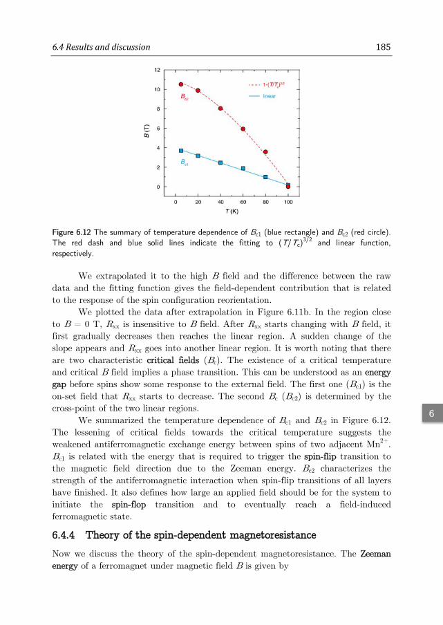
6.4Resultsanddiscussion 185
6
Figure 6.12 The summary of temperature dependence of Bc1 (blue rectangle) and Bc2 (red circle). The red dash and blue solid lines indicate the fitting to (T/Tc)
3/2 and linear function, respectively.
We extrapolated it to the high B field and the difference between the raw data and the fitting function gives the field-dependent contribution that is related to the response of the spin configuration reorientation.
We plotted the data after extrapolation in Figure 6.11b. In the region close to B = 0 T, Rxx is insensitive to B field. After Rxx starts changing with B field, it first gradually decreases then reaches the linear region. A sudden change of the slope appears and Rxx goes into another linear region. It is worth noting that there are two characteristic critical fields (Bc). The existence of a critical temperature and critical B field implies a phase transition. This can be understood as an energy gap before spins show some response to the external field. The first one (Bc1) is the on-set field that Rxx starts to decrease. The second Bc (Bc2) is determined by the cross-point of the two linear regions.
We summarized the temperature dependence of Bc1 and Bc2 in Figure 6.12. The lessening of critical fields towards the critical temperature suggests the weakened antiferromagnetic exchange energy between spins of two adjacent Mn2+. Bc1 is related with the energy that is required to trigger the spin-flip transition to the magnetic field direction due to the Zeeman energy. Bc2 characterizes the strength of the antiferromagnetic interaction when spin-flip transitions of all layers have finished. It also defines how large an applied field should be for the system to initiate the spin-flop transition and to eventually reach a field-induced ferromagnetic state.
6.4.4 Theory of the spin-dependent magnetoresistance
Now we discuss the theory of the spin-dependent magnetoresistance. The Zeeman energy of a ferromagnet under magnetic field B is given by

186 Chapter6
6
cos (6.11) where φ is the angle between external magnetic field B and magnetization M.
Below TC, Mn1/4TaS2 becomes ferromagnetic with easy plane normal to the direction of B. Thanks to its layered structure; the magnetization is mostly confined to the intercalated Mn layer. Initially, the magnetic moments of two adjacent planes are slightly canted, resulting in zero magnetization along the field direction (Fig. 6.13a). With an out-of-plane B field, because of large in-plane anisotropy, the spin cannot be aligned immediately to the field direction. Instead, spins with the magnetic moments direction that are energetically unfavorable will flip 180° in the plane and couple antiparallel to the spins of neighboring Mn plane (Fig. 6.13b).
With elevated temperature, the thermal fluctuation (kBT) perturbs the spin-flip transition, which is proportional to T. Therefore; we observed the linear dependence of the critical field Bc1 as a function of temperature.
Bc2 characterizes the energy barrier for phase transition from a spontaneous in-plane ferromagnetic phase into a field-induced out-of-plane spin-flop phase. From the magnetic susceptibility measurement (Fig. 5.12a), the magnetization increases rapidly close to TC, implying the spontaneous breaking of the global symmetry. Below TC, the increase of magnetization can be formulated by the Bloch 3/2 law, where describes the excitation of the spin waves at higher temperature. For a second-order phase transition between ferromagnetic state to antiferromagnetic state happens, we have
0 1 ⁄ / , (6.12) where Bc2(0) is the critical field for the antiferromagnetic ground state.
Figure 6.13 Schematic illustrations for initial state with spin canting (a) and after spin flip transition (b). The schemes are analogous to the giant magnetoresistance current in the plane geometry with low (c) and high (d) resistances.

6.4Resultsanddiscussion 187
6
From the fitting, we derived that the ground state critical field Bc2(0) for this intercalation concentration (x = 0.25) is 10.8 T and the critical temperature Tc is 101 K, which is almost identical to the Curie temperature we measured from the magnetic susceptibility measurement.
6.4.5 Angle-dependent magnetoresistance
To illustrate the energy gap of Bc1 is a temperature-dependent parameter that does not depend on the angle between the external magnetic field and magnetization, we performed the angle-dependent longitudinal magnetoresistance measurement.
Figure 6.14a summarizes the Rxx data for a series of angles θ between B and sample ab plane. It clearly shows that there is a significant anisotropy in terms of Rxx response to the field. For θ = 90°, with increasing B field, Rxx increases parabolically before decreasing dramatically. Changing θ gradually from 90° to 75° weakens this effect. For θ < 70°, the negative MR at large B diminishes, while a little decrease at small field emerges. This weak-localization-like MR behavior is linked to the alignment of spins. As we discussed before, there are excitation of spin waves at finite temperature that can be treated as spin canting off the field direction. Increasing B field, in turns, diminishes the spin waves as the canted angle approaching to zero.
We applied the same method to extract the spin-dependent signals from the raw data (Fig. S6.1). The results are shown in Figure 6.14b. We find that the energy gap corresponding to the Bc1 is angle dependent. With increase of θ, ∆Rxx first decreases then increases. This is because of the competition between the exchange interaction of two spins and the Zeeman energy of each spin.
Consider the energy of the whole system,
∙ ∙ 2 ∙
cos2
cos2
2 cos , (6.13)
where ϑ and ϕ are the angle between B and ab-plane and angle between two spins, respectively. When the free energy is minimized, we have
sin2
2sin
2. (6.14)
Clearly, θ depends on both ϕ and B. Therefore, it further demonstrates that the energy gap related to Bc1 is due to the spin-flip transition as a function of temperature and spin canting angle ϕ.
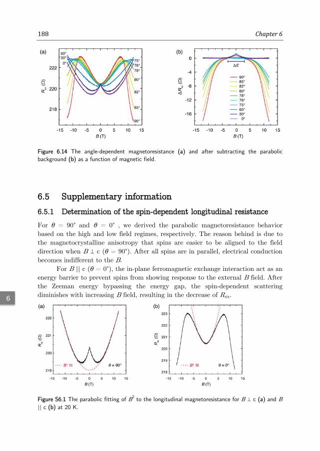
188 Chapter6
6
Figure 6.14 The angle-dependent magnetoresistance (a) and after subtracting the parabolic background (b) as a function of magnetic field.
6.5 Supplementary information
6.5.1 Determination of the spin-dependent longitudinal resistance
For θ = 90° and θ = 0° , we derived the parabolic magnetoresistance behavior based on the high and low field regimes, respectively. The reason behind is due to the magnetocrystalline anisotropy that spins are easier to be aligned to the field direction when B c (θ = 90°). After all spins are in parallel, electrical conduction becomes indifferent to the B.
For B || c (θ = 0°), the in-plane ferromagnetic exchange interaction act as an energy barrier to prevent spins from showing response to the external B field. After the Zeeman energy bypassing the energy gap, the spin-dependent scattering diminishes with increasing B field, resulting in the decrease of Rxx.
Figure S6.1 The parabolic fitting of B2 to the longitudinal magnetoresistance for B c (a) and B || c (b) at 20 K.

6.5Supplementaryinformation 189
6
6.5.2 Band structure of the Mn intercalated TaS2
In transition metal intercalated complexes, there has been ample evidence for charge transfer from the intercalated metal atoms to the matrix element (Nb, Ta), resulting in the change of oxidation state to +2 (or +3) for the intercalants. For example, when V or Cr is used as intercalant, the associated electrostatic coupling with the layers leads to a change in valence state of +3; whereas +2 for other elements, such as Mn and Fe. The remarkable difference between the magnetocrystalline anisotropy between Fe and Mn intercalated TaS2 is a result of orbital contributions.
Figure S6.2 Band structure of the manganese intercalated TaS2. (a) The 3d-band of Mn is overlapped with the 5d-band of Ta. The hybridized new d-band initiates the itinerant ferromagnetism in this material.
Mn1/4TaS2 originates from the 2H-TaS2 matrix, where the Ta atoms form trigonal prismatic with S atoms, resulting in a crystal field splitting of the Ta d-orbitals. Band calculation shows that only the lowest Ta d-band crosses the Fermi energy, providing metallic conductivity. For example, a unit cell of 2H-TaS2 has been known to exhibit charge-density-wave (CDW) phase [1]. The 5d-conduction band of TaS2 is half full and can accept maximum one more electron per Ta atom. The intercalated Mn atoms donate electrons to the TaS2 dz2 band, which is formed by the hybridization of dz2 and dx2-y2 [21] (Fig. S6.2).
There has been a long-lasting discussion about the magnetism mechanism of transition metal intercalated TMDs. X-ray circular dichoism (XMCD) and angle resolved photoemission spectroscopy (ARPES) measurement reveal that the magnetism of sister material Fe1/4TaS2 is due to the RKKY interaction [22]. There are also ample evidences from inelastic neutron scattering measurements showing that the magnon dispersion along the c-axis is much stronger than in the ab-plane, which contradicts the estimation based on RKKY assumption [23]. The present study successfully formulates the observed spin-dependent magnetoresistance with GMR-like theory, which implies that Mn 3d electrons should be treated as itinerant electrons.

190 Chapter6
6
6.5.3 Anomalous Hall effect of Mn1/4TaS2
Measurement of the transverse signal shows the anomalous Hall effect (AHE) below the critical temperature (160 K), which is a non-linear function of the applied B field. Empirically, AHE can be described by the formula:
, (6.15)
where B is the magnetic field, M the magnetization and R0, RA the ordinary and anomalous Hall coefficients, respectively. The first term denotes the ordinary Hall effect, the second term represents the effect from the magnetization and the third term considers the influence of the spin-texture.
From 160 K to 100 K (that is the TC of the material), the anomalous part increases with decreasing temperature, which is caused by the increase of paramagnetic magnetization. Below 100 K, the AHE becomes even more complicated. The influence of the M is not monotonic and there are two effects acting on Rxy with opposite signs (Fig. S6.3). On the other hand, no signal could be obtained for B c. This is because the sample was placed with the current direction I || B, so that no planar Hall effect could be measured (see chapter 4).
.
Figure S6.3 The temperature-dependent anomalous Hall effect as a function of magnetic field. The red and blue lines show the behaviors with B || c and B c, respectively.

6.6Summary 191
6
6.6 Summary Mn1/4TaS2 has a magnetic easy plane, where magnetic moments of Mn form ordered state parallel to the crystal layer simultaneously. When an out-of-plane magnetic field is applied, the spins are difficult to be aligned to the field direction directly. Instead, two spin-dependent processes happen with increase of field. From the temperature-dependent magnetoresistance measurement, we derived two critical fields that correspond to spin-flip (Bc1) and spin-flop (Bc2) transitions. This significantly spin-dependent process is due to the magnetocrystalline anisotropy. From the angle-dependent magnetoresistance measurement, we found that the Bc1
is a function of both B and spin canting angle ϕ. The appearance of anomalous Hall effect further demonstrates the emergence of magnetic ordering.

192 Chapter6
6
6.7 References [1] Yu Y, Yang F, Lu XF, Yan YJ, Cho Y-H, Ma L, Niu X, Kim S, Son Y-W,
Feng D, Li S, Cheong S-W, Chen XH, Zhang Y, "Gate-tunable phase transitions in thin flakes of 1T-TaS2", Nat Nanotechnol 10, 270-6 (2015).
[2] Sipos B, Kusmartseva AF, Akrap A, Berger H, Forró L, Tutiš E, "From Mott state to superconductivity in 1T-TaS2", Nat Mater 7, 960-5 (2008).
[3] Parkin S, Marseglia EA, Brown PJ, "Magnetisation density distribution in Mn1/4TaS2: observation of conduction electron spin polarisation", Journal of Physics C: Solid State Physics 16, 2749-64 (1983).
[4] Motizuki K, Suzuki N, Tomishima S, "Itinerant magnetism of Mn-intercalated compounds of 2H-type TaS2", J Magn Magn Mater 104-107, 681-2 (1992).
[5] Dijkstratg J, Zijlemat PJ, van Bruggent CF, de Haas C, de Groot RA, "Band-structure calculations of Fe1/3TaS, and Mn1/3TaS, and transport and magnetic properties of Fe0.28TaS2", J Phys: Condens Matter 1, 6363-79 (1989).
[6] Choi YJ, Kim SB, Asada T, Park S, Wu W, Horibe Y, Cheong S-W, "Giant magnetic coercivity and ionic superlattice nano-domains in Fe0.25TaS2", EPL 86, 37012 (2009).
[7] Vannette MD, Yeninas S, Morosan E, Cava RJ, Prozorov R, "Local-moment ferromagnetism and unusual magnetic domains in Fe1/4TaS2 crystals", Phys Rev B 80, 024421 (2009).
[8] Morosan E, Zandbergen HW, Li L, Lee M, Checkelsky JG, Heinrich M, Siegrist T, Ong NP, Cava RJ, "Sharp switching of the magnetization in Fe1/4TaS2", Phys Rev B 75, 104401 (2007).
[9] Sun C, Kono J, Imambekov A, Morosan E, "Anomalous magneto-optical Kerr hysteresis loops in Fe0.25TaS2", Phys Rev B 84, 224402 (2011).
[10] Checkelsky JG, Lee M, Morosan E, Cava RJ, Ong NP, "Anomalous Hall effect and magnetoresistance in the layered ferromagnet Fe1/4TaS2: The inelastic regime", Phys Rev B 77, 014433 (2008).
[11] Zhu XD, Sun YP, Zhang SB, Lei HC, Li LJ, Zhu XB, Yang ZR, Song WH, Dai JM, "Superconductivity and single crystal growth of Ni0.05TaS2", Solid State Commun 149, 1296-9 (2009).
[12] Li LJ, Zhu XD, Sun YP, Lei HC, Wang BS, Zhang SB, Zhu XB, Yang ZR, Song WH, "Superconductivity of Ni-doping 2H–TaS2", Physica C: Superconductivity 470, 313-7 (2010).
[13] Wagner K, Morosan E, Hor Y, Tao J, Zhu Y, Sanders T, McQueen T, Zandbergen H, Williams A, West D, Cava R, "Tuning the charge density wave and superconductivity in CuxTaS2", Phys Rev B 78, 104520 (2008).

6.7References 193
6
[14] Parkin SSP, Friend RH, "3d transition-metal intercalates of the niobium and tantalum dichalcogenides. I. Magnetic properties", Philosophical Magazine B 41, 65-93 (1980).
[15] Chhowalla M, Shin HS, Eda G, Li LJ, Loh KP, Zhang H, "The chemistry of two-dimensional layered transition metal dichalcogenide nanosheets", Nat Chem 5, 263–75 (2013).
[16] Geim A, "Graphene: exploring carbon flatland", Physics today 60, 35 (2007). [17] Wallace PR, "The band theory of graphite", Phys Rev 71, 622 (1947). [18] Slonczewski JC, Weiss PR, "Band structure of graphite", Phys Rev 109, 272
(1958). [19] Mott NF, "The electrical conductivity of transition metals", Proc R Soc A
153, 699 (1936). [20] Hiroshi Y, Satoshi T, "Magnetoresistance of antiferromagnetic metals Due to
s-d Interaction", J Phys Soc Jpn 34, 51-7 (1973). [21] Di Salvo FJ, Hull Jr GW, Schwartz LH, Voorhoeve JM, Waszczak JV,
"Metal intercalation compounds of TaS2: preparation and properties", J Chem Phys 59, 1922-9 (1973).
[22] Ko KT, Kim K, Kim SB, Kim HD, Kim JY, Min BI, Park JH, Chang FH, Lin H, Tanaka A, Cheong SW, "RKKY ferromagnetism with Ising-like spin states in intercalated Fe1/4TaS2", Phys Rev Lett 107, 247201 (2011).
[23] Cussen LD, Marseglia EA, Paul DM, Rainford BD, "Magnon dispersion in Mn1/4TaS2", Physica B 156-157, 712-4 (1989).


In preparation: Lei Liang, Qihong Chen, Graeme R. Blake, Thomas T. M. Palstra, Jianting Ye – “A magnetically responsive one-dimensional mesoporous material functionalized with paramagnetic ionic liquid”
Chapter 7
A magnetically responsive one‐dimensional mesoporous material functionalized with paramagnetic ionic liquid
agnetism is generally regarded as intrinsic property of
materials and cannot be changed when the material
has been synthesized. Magnetic phase transition occurs only
when the ordering temperature has been reached by
competing with the thermal energy. In this chapter, we show
that paramagnetic to ferromagnetic phase transition can be
achieved by mesoscopic structural confinement. The
imidazolium-based ionic liquids that contain transition metal
complex as anions show paramagnetism at room temperature.
However, when this kind of paramagnetic ionic liquids are
confined into the mesoporous silica template by
ultrasonication under vacuum, they become ferromagnetic.
This transition was demonstrated by the elevated glass
transition temperature and hysteresis in the magnetization
curve.
M

196 Chapter7
7
7.1 Introduction
7.1.1 Porous material
Porous materials are of great interests in many applications. A porous medium contains pores with various sizes. According to IUPAC notation, three categories of porous materials can be named based on their pore diameters (Tab. 7.1).
There are many macroporous materials exist in nature with pore size bigger than 50 nm. Many biological reaction and processes rely on these pores because the pore diameter is comparable to the wavelength of the visible light. For example, diatom is one of the largest species around the world (Fig. 7.1a). It is particular important for the ocean, which contributes more than 45% of the primary production of organic materials. Once they become dead, after millions of years, the silica based cell wall (frustule) turns into an important mineral, the diatomaceous earth, which preserves the shape of the diatom cell (Fig. 7.1b). In recent years, diatomaceous earth receives enormous interests for its significant importance in oil industry, chemical engineering, civil engineering and so on, such as catalytic medium [1], purification filter [2]and even energy storage materials [3].
Microporous materials contain pores with diameters less than 2 nm. Than are often used in laboratory for the purpose of trapping, such as ions, gas molecules and bacteria. The common examples include zeolites [4] and metal-organic frameworks [5]. Mesoporous materials are those contain There are many ordered silicon based minerals exist in nature.
Table 7.1 Classification of porous materials based on pore diameters (IUPAC notation).
Materials Macroporous Mesoporous Microporous
Pore size (nm) > 50 2-50 < 2
Figure 7.1 (a) Optical microscopic image of a diatom cell. (b) Scanning electron microscopic image of diatomaceous earth. (Images are taken from Internet individually)

7.1Introduction 197
7
Figure 7.2 Mean-field prediction of the thermodynamic equilibrium phase structures for conformationally symmetric block-copolymer melts. Phases are labeled as: S (body-centered cubic spheres), C (hexagonal cylinders), G (bicontinuous cubic), L (lamellae). fA is the volume fraction of component A. (Figure was modified from ref. [6])
7.1.2 Synthesis of mesoporous material using block-copolymer
Copolymer is a kind of polymer that is polymerized with more than two kinds of monomers. The monomers have double-bond or triple-bond that allow cross-linking reaction with one another to form large network. It has of great interest in using as template for fabricating structures in nanoscale.
The packing of molecules follows the thermodynamics, where the energy in the mixing state of block-copolymer is determined by the enthalpy gain and entropy cost. Practically, the molecular weight, volume fraction of the component and the degree of segment incompatibility are three independent parameters that relevant to the final thermodynamically stable morphologies. Figure 7.2 illustrates the transition of the formed nanostructures by mixing polymer A and B as a function of the volume fraction of component A (fA). With increase of fA, a variety of morphologies can be formed, which are body-centered cubic spheres, hexagonal cylinders, bicontinuous cubic and lamellae.
7.2 Concepts 7.2.1 Phase transition of ionic liquid
Ionic liquids receive much attention recently due to their unique properties of strongly polarized charge separation under room temperature. In chapter 1, we have introduced the main difference between ionic liquid and the conventional molten salts, where the former one are composed of large asymmetrical ions that are bonded loosely with each other. Because of that, many ionic liquids are difficult to crystallize simply by cooling, while they form glass instead. In order to obtain their crystal structure, particular technique such as in-situ crystallization method is proposed [7].

198 Chapter7
7
Figure 7.3 Characterization of the phase transition process in polymers with differential scanning calorimetry. During warming up, the frozen polymer experiences a sequence of processes. First the chain of polymer starts to be mobile again and glass transition happens. The polymer changes from glass-like solid to rubber-like soft form. Then it might crystallize or directly melting at higher temperature.
In this method, a Bridgeman type of geometry has been used. Ionic liquid is sealed in a glass tube and frozen by cryogen gas initially. A laser is installed to heat the sample locally. The laser spot melts a small domain and the temperature gradient creates a solid/liquid interface so that the crystal can grow starting there. Laser is moving downward slowly in order to crystalize the ionic liquid of the whole tube. In this way, the glass formation process can be bypassed and single crystal X-ray diffraction measurement can be performed thereafter.
The thermal history also influences the phase transition of ionic liquid. As shown in Figure 1.10 and also reported by others [7], some ionic liquids crystalize during warming up before melting at higher temperature; whereas others experience a glass transition into some rubber-like high viscosity state.
7.2.2 Synthesis of SiO2-based mesoporous template
Prior to the present used mesoporous silica template SBA-15 (Santa Barbara Amorphous No.15) [8], MCM-41 (Mobil Composition of Matter No. 41) was the most famous hexagonally ordered molecular sieve discovered by Mobil Oil Corporation in 1992 . The synthesis is based on cetyltrimethylammonium bromide (CTAB) as surfactant template. Due to its smaller size, the pore dimension of the MCM-41 is normally only 2-3 nm. In order to increase the pore size, amphiphilic polymers with larger molecular weight are expected to extend the mesoporous length scale.
The template agent we used for the following synthesis involves using a symmetric triblock copolymer constitutes of poly(ethylene oxide)(PEO) and poly

7.3Experiments 199
7
(propylene oxide) (PPO), namely pluronic P-123. The nominal chemical formula is HO(CH2CH2O)20(CH2CH(CH3)O)70(CH2CH2O)20H, which corresponds to a molecular weight of around 5800 g/mol. The silica precursor is tetraethyl orthosilicate (TEOS) with the formula Si(OC2H5)4, which is the ethyl ester of orthosilicic acid Si(OH)4.
P-123 has the behavior similar to those hydrocarbon surfactants, which will form micelles when is placed in polar solvent such as water. Depending on the concentration, they are capable of forming spherical or cylindrical micelles. These micelles are used as the backbone to synthesize structured mesoporous materials.
TEOS is the most commonly used crosslinking agent for synthesis of silicon dioxide based on the hydrolysis reaction. When TEOS is reacted with water, the O-R bond in Si(O-R)4 is attacked by H-OH and converted into Si(OH)4 and RH. Si(OH)4 is not stable and will further change to SiO2. Depending on the reaction rate and condition, the resulted SiO2 can be powder, thin film, gel and even highly porous aerogel. This hydrolysis reaction is also called sol-gel reaction.
Figure 7.4 Constitutions of chemical compounds for the synthesis: P-123 and TEOS.
Figure 7.5 Schematic illustration of the polymerization process where P-123 block-copolymer aggregates into cylinder morphology at acidic condition.
Figure 7.6 Sol-gel reaction of silica porous material based on hydrolysis of TEOS.

200 Chapter7
7
7.3 Experiments
7.3.1 Synthesis of SBA-15 mesoporous silica
In order to acquire silica gel without aggregating into condensed powder, acidic condition is necessary. The precursors we used are P-123, TEOS, hydrochloric acid (HCl, 37 wt%), and deionized water (DI H2O). The sequences and speed of adding ingredients are the key for successful synthesis. We first dissolved 4 g P-123 into 15 ml HCl and 85 mL DI H2O, forming 1.5 mol/L of solution A.
Afterward, 8.5 g TEOS (98 wt%) was slowly added (drop by drop) to the solution A under vigorous stirring at 2000 rpm. White gel started to form when TEOS was contacted with acidic solution A.
Later on, the as-prepared white gel (with solution) was transferred to a Teflon autoclave and sealed with steal kettle for aging. The kettle was put into oven with the hydrothermal condition at 110 °C for 24 h.
Once the aging was finished, the product was collected by centrifuge. The product was further washed with DI H2O and dried at 60 °C in a form of white powder. At this moment, surfactant P-123 still remained in the product and needed to be removed.
We put the white powder in an Al2O3 crucible and calcinated in a muffle oven in the air at 550 °C for 6 h. The resulted final product was SBA-15 template.
Figure 7.7 Schematic illustration of the synthesis of SBA-15 silica template based on P-123 surfactants.
7.3.2 Encapsulation of paramagnetic ionic liquid
One gram of SiO2 nanosphere was placed in a two-neck round bottom flask with one neck sealed by rubber cork and the other neck connected to a mechanical pump. The powder was later vacuumed carefully without being blown away.
Figure 7.8 Illustration of the vacuum encapsulation process, where paramagnetic ionic liquid molecules are absorbed within the pores of the SBA-15 silica template.

7.3Experiments 201
7
Then, about 20 ml of BMIM[FeCl4] paramagnetic ionic liquid (PIL) was syringe-injected into the flask to fully immerse the powder. In this step, it is better to avoid direct drop of PIL on the powder in order to prevent splashing powder everywhere on the wall of flask.
Afterwards, the flask was put in an ultrasonic bath and heated in silicone oil at 120-170 °C for 12-48 h. Ultrasonication was maintained during the heating process to facilitate the diffusion of PIL molecule into the pore of SBA-15.
The encapsulation process was terminated by stopping ultrasonication and heating. After the flask was cooled down back to room temperature,
7.3.3 Synthesis of SiO2 nanospheres as comparison
SiO2 nanospheres were synthesized for comparison purpose. Basic environment (pH > 12) was required for the deposition of SiO2 nanosphere. We prepared the medium with ammonia (NH3·H2O), ethanol (EtOH) and DI H2O. To aim particle size of 80 nm, the molar ratio between TEOS and DI H2O is 1 : 2, so that the usage of TEOS, NH3·H2O and DI H2O respect to 60 mL EtOH were 12 mmol , 60 mmol and 120 mmol, respectively. Since all precursors are in liquid form at room temperature, the volumes for TEOS and NH3·H2O (25 wt%) were 1 mL, 4 mL, respectively.
The mixture was sealed in a 100 ml round bottom flask with rubber cork and magnetic stirred at room temperature for 96 h at 600 rpm. Afterward, the stirring was stopped and the deposition was further grown with Ostwald ripening process for 30 h. Later, the white deposition was separated by centrifuge and dried in the oven. In the end, the powder was calcined in the air at 550 °C for 12 h.
Identical method was used for encapsulation attempt. In the end, the obtained sample was collected for the magnetic measurement.
7.3.4 Transmission electron microscopy
Transmission electron microscope (TEM) was used to characterize the morphology and pore size of the calcined SBA-15 including different sample orientations. TEM specimens were prepared as follows. SBA-15 powders were first dispersed in absolute ethanol, followed by dropping one droplet onto a piece of TEM copper grid and naturally dried. Specimens were analyzed using JEOL JEM2010 microscopes with LaB6 filament at 200 kV. The images were collected by Gatan Erlangshen CCD camera.
Figure 7.9a shows well-ordered hexagonal arrays of mesopores. We analyzed the TEM image with the Digital Micrograph software and it shows that the distance between mesopores is estimated to be 5 nm (Fig. 7.9b).

202 Chapter7
7
Figure 7.9 (a) Transmission electron microscopic image of calcinated SBA-15 mesoporous silica with cylinder structure. Yellow line indicates the part where the pore size was determined. (b) The pore size profile of the sample shown in the TEM image. The average pore size is around 5 nm. (c) TEM images of overlapped two particles, showing hexagonal pore configuration. (d) Low resolution TEM image shows the size of a single particle. (Images was taken by Dr. Bin Chen from University of Groningen.)
7.3.5 Raman spectra of PIL and PIL@SBA-15
To study the mechanism of magnetic interaction between neighbouring magnetic centers, we performed the Raman spectroscopy measurement. The Raman signal was excited by a Cobolt Samba 25 diode pumped solid-state green lasers with wavelength of 532 nm. The laser light was passed through two pinholes and a line filter. Then, the light was focused on sample carried by a silicon wafer through a microscope with maximum ×100 objective lens. The laser power at the sample was about 0.4 mW.
Scattered light was collected at about 30° from the excitation beam, collimated, passed through a superholographic notch filter, and sent into a spectrometer (ANDOR, model: SR-500i-D1-R). The light was dispersed via 600 to 1800 lines/mm grating and detected via a Peltier-cooled CCD (ANDOR, model: DV420A-OE). Spectral positions and intensity were calibrated referring to the spectrum of Si before the measurement of ionic liquid samples. The signal was

7.3Experiments 203
7
subtracted from the background. Sometimes there will be some spike peak due to “cosmic rays”. We repeatedly took the background until there were no spikes. The collection time was 30 s.
Figure 7.10 shows the Raman spectra of difference polarization angles. We noticed that there were two characteristic peaks at wavenumber around 150 cm-1
and 350 cm-1. They belong to the vibrational modes of FeCl4- ion. The high
wavenumber peaks are due to the stretching modes, with symmetric and asymmetric vibration modes at 331 cm-1 and 390 cm-1, respectively. The peaks at 116 cm-1 and 166 cm-1 are related to the bending mode of the Fe-Cl bond [9].
Interestingly, the relative intensity between bending and stretching modes changes with respect to the linear polarization angle. When the analyzer is aligned with the laser polarization, the maximum Raman scattering is observed for stretching mode. Rotating the polarizer leads to the ratio between the crossed intensity over aligned intensity (depolarization ratio) approaches zero. However, while intensity of the peaks corresponding to the stretching mode extinguishes, the intensity of the bending mode peaks enhances.
For isotropic samples, the Raman spectra are not sensitive to the orientation of the polarized light. Normally, liquids are regarded as isotropic, hence should be weak polarization dependence. However, here we found that paramagnetic ionic liquids are very sensitive to the polarized light, with depolarization ratio almost equals to zero. This discovery indicates that ionic liquids show some properties that only crystals have even with quite low viscosity.
Figure 7.10 Raman spectra taken with linear polarized incident light. The crossed angles between the analyzer and the Raman scattered light are labeled on the right. Peaks corresponding to different vibration modes are indicated with dash lines.

204 Chapter7
7
7.4 Results and discussion
7.4.1 Magnetic susceptibility measurement
In chapter 1 and 4, we have discussed the paramagnetic nature of PIL. Magnetic susceptibility of pristine BMIM[FeCl4] follows Curie’s law with weak antiferromagnetic interaction below 80 K (Fig. 4.10b). However, BMIM[FeCl4]@SBA-15 sample reveals evidences of magnetic ordering. The inverse magnetic susceptibility shows deviation downwards from the Curie-Weiss law (Fig. 7.11b), which is indicative of the onset of a net magnetic moment below some critical temperatures [10].
Figure 7.11 (a) Normal and (b) Inverted magnetic susceptibility of BMIM[FeCl4]. The purple line shows the linear fitting to the high temperature region.
7.4.2 Magnetization curve of PIL@SBA-15
In order to confirm the emergence of ferromagnetic state at low temperature, we measured the magnetization curve of PIL@SBA-15 at 20 K. Over the applied magnetic field range from -2 T to 2 T, it shows a non-linear field dependency, which is significantly different from the pristine PIL (Fig. 7.12a).
We further demonstrated the emergence of ferromagnetism was due to SBA-15 mesoporous, rather than side reaction with SiO2. By applying the identical method of encapsulation to SiO2 nanosphere, we are not able to repeat the observation of hysteresis at same temperature (Fig. 7.12b). This control experiment strongly confirmed the indispensable prerequisite of SBA-15 in inducing ferromagnetism in BMIM[FeCl4].

7.4Resultsanddiscussion 205
7
Figure 7.12 The magnetization curve of PIL@SBA-15 (a) and PIL+SiO2 nanosphere (b), where the former one shows non-linear field dependence of the magnetization. The inset shows the hysteresis loop after subtracting the linear paramagnetic background at high B field.
7.4.3 Magnetization curve of the precursors
To exclude the possible reason that ferromagnetic impurities cause the magnetic response after encapsulation, we measured the magnetization curves of the precursors prior to the encapsulation process. Figure 7.13 shows three magnetization curves measured at 20 K. The ones of FeCl3 and BMIM[FeCl4] are almost identical to each other, demonstrating that the paramagnetic nature of ionic liquid is conveyed by Fe3+ in FeCl4
- anion. In addition, no hysteresis was found to the best of experiment resolution, which eliminated the possibility of ferromagnetic impurity contamination from the results. On the other hand, SBA-15 silica template shows weaker diamagnetic behavior that cannot contribute much to the magnetization of encapsulated product.
To exclude the possibility of BMIM[FeCl4] degradation during heating and form ferromagnetic impurity, we measured the PIL heated in the air at 120 °C and sample showed identical behavior as Figure 7.13b.
Figure 7.13 Magnetization curve of anhydrous FeCl3 (a), as-synthesized BMIM[FeCl4] (b) and SBA-15 silica template (c) at 20 K.

206 Chapter7
7
7.4.4 Low temperature differential scanning calorimetry
Phase transitions of PIL after encapsulated in SBA-15 nanopores can be reflected in the differential scanning calorimetry measurement. We determined that the melting temperature Tm of pure BMIM[FeBr4] is about 0 °C. After encapsulation, Tm of the composite material PIL@SBA-15 increases to 35 °C. This indicates that the new form of PIL possesses a much better thermal stability (Fig. 7.14).
The melting temperature of ionic liquids is the combination effect of the electrostatic Coulomb interaction, hydrogen bonding and van der Waals forces. SBA-15 templates offer atomically thin one-dimensional channels that restrict the ionic orientation [11]. The enhancement of the inter-molecular interaction increases the stability of the encapsulated PIL.
Figure 7.14 Low temperature differential scanning calorimetry curve for BMIM[FeCl4] before (in blue) and after (in red) encapsulated into SBA-15 template.
7.4.5 Raman spectrum of PIL@SBA-15
Figure 7.15 Raman spectrum of PIL@SBA-15 taken without polarizer. The sample shows strong photoluminescence and the fringes at low wavenumbers are due to the interference of light.

7.4Resultsanddiscussion 207
7
We attempted to resolve the change of molecular vibrations after encapsulated in SBA-15, however, due to the strong photoluminescence (PL) of mesoporous SiO2, we are not able to recognize the peaks of PIL from the strongly enhanced background. The PL signal of SiO2 nanotubes has been reported by others [12, 13].
7.4.6 Plausible explanation of one-dimensional ferromagnetism
Because of high uniaxial magnetic anisotropy, one-dimensional (1D) magnets are attracted growing interests in information storage area. 1D magnets are often based on organic molecules [14, 15]. Single chain magnets of inorganic compounds promise to have stronger exchange interaction. However, The inorganic supramolecules are easily aggregated and form 3D structure.
Considering the distances between two nearest magnetic centers (Fe3+) are in the order of 10 Å, pristine BMIM[FeCl4] show no magnetic exchange interaction and behaves as paramagnet. However, a similar molecule 1-ethyl-3-methylimidazolium tetrachloroferrate (EMIM[FeCl4]) shows antiferromagnetism below 4 K, which is due to the Fe-Cl−Cl-Fe super-exchange pathway [16]. Because of the smaller chain length of the organic cation (from butyl- to ethyl-), the antiferromagnetic interaction is stronger in EMIM[FeCl4] and can be measured at relatively high temperature. There has been study of pressure-induced three-dimensional long-range magnetic ordering in EMIM[FeCl4] under high pressure. It was found that under intermediate pressure (0.3 GPa < P < 1 GPa), the sample showed ferromagnetism; while above or below the pressure, the sample showed antiferromagnetism [9].
It is worth noting that the surface of SiO2 is terminated by -OH group, which could react with FeCl4
-. In the end, FeCl4- will be reduced to Fe2+Cl3
- (Fig. 7.16a). However, Fe2+Cl3
- is not stable and behaves as a Lewis base. It is very likely that Fe2+Cl3
- will bond with Fe3+Cl4- to form a dimer in order to lower the
negative charge (Fig. 7.16b). Formation of dimer Fe2Cl72-, a discrete form of FexCly,
with both Fe3+ and Fe2+ is the building block of the 1D ferromagnetic chain. To our knowledge, same single chain ferromagnetism has also been reported for (H2melamine)2[FeCl5]Cl [17].
Fe3+ has the high-spin state, with the crystal field of both t2g and eg orbitals half-occupied. Mediated by the Cl-, the electron of Fe3+ can hop to Fe2+ with the spin direction preserved. This is due to the Hund rule (first), and Pauling exclusion principle. This indirect exchange interaction is called double-exchange mechanism and couples the spin of two Fe ions with different valence states (Fig. 7.16c).

208 Chapter7
7
Figure 7.16 (a) Reduction reaction of FeCl4- at SiO2 surface, producing unstable Fe2+Cl3
-. (b) Mechanism of double-exchange interaction between Fe3+ and Fe2+. (c) Molecular structure of the dimer product. (d) Formation of one-dimensional ferromagnetic chain.
Thanks to the channel structure of SBA-15 and particular pore diameter; only Fe contained ions are capable of encapsulation. Due to the structural constrain, the bonding between Fe2+ and Fe3+ complexes cannot be relaxed in all directions, instead, they have to be elongated along the channel direction. Therefore, the observed phenomenon seems to suggest that the double-exchange pathways mediated through Fe3+–Cl–Fe2+ are responsible for the appearance of magnetic ordering (Fig. 7.16d).
7.5 Summary Encapsulation of paramagnetic ions inside nanostructures is capable of inducing long range magnetic ordering. The BMIM[FeCl4] encapsulated SBA-15 silica template with pore size of 5 nm shows hints of ferromagnetic ordering at low temperature. The ferromagnetic state has been evidenced by the magnetic susceptibility measurement, which shows deviation from the Curie’s law for paramagnetism. Magnetization curve at 20 K shows hysteresis loop after subtracting the paramagnetic background. Low temperature DSC measurement further supports the enhanced inter-molecular interaction with increased melting temperature. Possibilities of ferromagnetic impurity contamination are excluded, where precursors show no divergence from the linear field dependence of magnetization. We ascribed the emergent magnetic ordering as a result of double-exchange mediated through Fe3+–Cl–Fe2+, resulted in one-dimensional ferromagnetic chain.

7.6References 209
7
7.6 References [1] Bao Z, Weatherspoon MR, Shian S, Cai Y, Graham PD, Allan SM, et al.,
"Chemical reduction of three-dimensional silica micro-assemblies into microporous silicon replicas", Nature 446, 172-5 (2007).
[2] Sermwittayawong D, Jakkawanpitak C, Waji N, Hutadilok-Towatana N, "Economical method for midiprep plasmid DNA purification using diatomaceous earth", ScienceAsia 39, 631-5 (2013).
[3] Shen L, Guo X, Fang X, Wang Z, Chen L, "Magnesiothermically reduced diatomaceous earth as a porous silicon anode material for lithium ion batteries", J Power Sources 213, 229-32 (2012).
[4] Davis ME, Lobo RF, "Zeolite and molecular sieve synthesis", Chem Mater (1992).
[5] Li H, Eddaoudi M, O'Keeffe M, Yaghi OM, "Design and synthesis of an exceptionally stable and highly porous metal-organic framework", Nature 402, 276-9 (1999).
[6] Li M, Ober CK, "Block copolymer patterns and templates", Materials Today 9, 30-9 (2006).
[7] Choudhury AR, Winterton N, Steiner A, Cooper AI, Johnson KA, "In-situ crystallization of low-melting ionic liquids", J Am Chem Soc 127, 16792-3 (2005).
[8] Zhao D, Feng J, Huo Q, Melosh N, Fredrickson GH, Chmelka BF, et al., "Triblock copolymer syntheses of mesoporous silica with periodic 50 to 300 angstrom pores", Science 279, 548-52 (1998).
[9] García-Saiz A, de Pedro I, Blanco JA, González J, Fernández JR, "Pressure effects on Emim[FeCl4], a magnetic ionic liquid with three-dimensional magnetic ordering", The Journal of Physical Chemistry B 117, 3198-206 (2013).
[10] Farokhipoor S, Magén C, Venkatesan S, Íñiguez J, Daumont CJM, Rubi D, et al., "Artificial chemical and magnetic structure at the domain walls of an epitaxial oxide", Nature 515, 379-83 (2014).
[11] Chen S, Wu G, Sha M, Huang S, "Transition of ionic liquid [Bmim][PF6] from liquid to high-melting-point crystal when confined in multiwalled carbon nanotubes", J Am Chem Soc 129, 2416-7 (2007).
[12] Li GH, Ding K, Chen Y, Han HX, Wang ZP, "Photoluminescence and Raman scattering of silicon nanocrystals prepared by silicon ion implantion into SiO2 films", J Appl Phys (2000).
[13] Chang HJ, Chen YF, Lin HP, Mou CY, "Strong visible photoluminescence from SiO2 nanotubes at room temperature", Appl Phys Lett (2001).
[14] Hirjibehedin CF, Lin CY, Otte AF, Ternes M, Lutz CP, Jones BA, et al., "Large magnetic anisotropy of a single atomic spin embedded in a surface molecular network", Science 317, 1199-203 (2007).

210 Chapter7
7
[15] Miller JS, "Magnetically ordered molecule-based materials", Chem Soc Rev 40, 3266-32 (2011).
[16] de Pedro I, Rojas DP, Albo J, Luis P, Irabien A, Blanco JA, et al., "Long-range magnetic ordering in magnetic ionic liquid: Emim[FeCl4]", J Phys: Condens Matter 22, 296006 (2010).
[17] Weng D-F, Wang B-W, Wang Z-M, Gao S, "(H2mela)2[FeCl5]Cl (mela=melamine): A Cl-bridged single-chain magnet based on weak ferromagnetism", Coord Chem Rev 257, 2484-90 (2013).

Submitted to Nature Communication: Lei Liang, Juan Shan, Qihong Chen, Jianming Lu, Graeme R. Blake, Thomas T. M. Palstra, Gerrit E. W. Bauer, Bart J. van Wees, Jianting Ye– “Gate-controlled spin-dependent magnetoresistance of a platinum/paramagnetic insulator interface”, 2017
Appendix
Device Fabrication Techniques and Transport Measurement Facilities
hysics in low dimensions often exhibits exotic
phenomenon that is different from the large scale. To
study how the magnetism in condensed matters behaves
when confined in two-dimensional system is the motivation of
this thesis. The devices studied in this thesis were all fabricated
in sub-micron scale. Because of the small size of the device,
the absolute value of the signal is often smaller compared to
bulky samples. Therefore, it also requires sensitive electrical
measurement technique in order to detect the subtle
changes when some effects occur. Here, I will mainly focus on
the basic steps of micro-fabrication techniques and the
principle of lock-in detection.
P

212 Appendix
A
A.1 Micro-fabrication
A.1.1 Electron beam lithography
Electron beam lithography, often abbreviated as EBL, is a high versatile technique for designing the electric circuit at nanoscale. It sits at the center of the modern micro-fabrication process, where many other relevant steps require successful EBL writing with as much as high resolution.
The EBL system contains two parts: one imaging system and one patterning system. The imaging system is a standard scanning electron microscope, which has an acceleration voltage up to 30 kV. The patterning system relies on the precise movement of the sample stage. During exposure, the electron-beam is fixed in one direction, and the sample moves with stage to the desired position. There are several useful concepts used in EBL and will be explained briefly as follows. UV coordinates. It is important to let the system know the correlation
relation between the stage position (XY coordinate) and the sample design (UV coordinate). Under two dimensions, three points will determine a plane. So in this step, we consequently look for three characteristic positions in the imaging system with their relative distances known. Normally, these positions will be three big makers in our pre-defined coordinating system. After locating one position, we adjust the UV coordinates to this position.
Write-field alignment. In order to let the system knows exactly where should the electron beam go, it is necessary to calibrate the beam with the marker on the wafer. We do two steps alignment. First, before we start setting the 3 points for building up the UV coordinate, we align roughly at a “dummy wafer” with some patterns on it far away from the as-exposed wafer. The purpose is to limit the chance of exposure of the device by mistake. The reason is that for each alignment, the imaging system has to peep the actually spotted position the electron beam locates. Although it is not a really high dose exposure, the resist can still react with the electron. Sometimes when the alignment of the beam is really poor, the adjustment distance of can be very large, which will cause the unexpected exposure. Second, we use the local marker close to the desired exposure position to do a fine alignment again to make sure the accuracy of the following writing.
Working area. It defines the area that will be exposed in one step. Normally, the size should be equal to or smaller than the write-field. There will be problem if the size is bigger than the write-field, because then the working area will be divided into several small pieces according to the size of the write-field and the center of the first piece will be away from the desired position, causing shift of the whole structure.
Stitching. It is not always feasible to put all structures in one working area without sacrificing the accuracy. Because in this case, we are forced to use

A.1Micro‐fabrication 213
A
large write-field in order to fit the working area without position shift. However, large write-field means the beam will be diverted by the electromagnetic field to reach the outskirt of the write-field, which will cause the misalignment to the design. In order to solve this problem, we use stitching technique. The idea is to divide large structure into smaller working areas manually and overlap each one a little bit with its adjacent neighbor. For example, in Figure A.2a, we show the design of our Pt EDLT. The electrical contacts are divided into a small and big structure, respectively (Fig. A.2b, c). For the small (big) structure, the working area (and equals to the write-field) is 120 μm (600 μm) and the stage movement is 115 μm (580 μm), which leads to 5 μm (20 μm) stitching area. This technique will prevent the contact discontinuity caused by inaccurate writing when two working areas are placed next to each other. The time to expose a given area for a given dose is given by the following
formula:
D × A = t × I (A.1)
where D is the dose, A the exposed area, t the time and I the beam current. For minimizing the exposure time, we use as large current as possible. However, larger current causes more serious proximity effect that will broaden the structure. Since current is proportional to the aperture size, in addition, larger aperture will also lead to bigger exposure variation.
Another factor determining the time is the dose. The dose reflects the electron interaction strength with the resists. Depending on the acceleration voltage, electrons interact stronger or less with the resist. This can be in analog to the bullets. High acceleration voltage leads to electrons with high kinetic energy that as well as the Different resists or substrates require different recipes. Before writing structures of new system, dose test is always recommended. The recipes of various resists used in this thesis are listed as follows.
In our institute, a Raith eLiNE lithography system is used for writing features with accuracy as high as 20 nm using small aperture (10 μm) and write field as large as 2.4 mm.
Before loading the wafer into the system chamber and exposing with electron beam (e-beam), we must design the structures first. Our group developed a technique using AutoCAD software to design the EBL structure. This software especially benefits the electrode design of layered material microflakes. By aligning the photos of flakes on marked wafer taken under microscope with the pre-defined coordinate system we input into AutoCAD, we can easily draw the electrical leads and bonding pads without interfering with dirts and other impurities en route. At last, we converted the file format from .dwg into .dxf and upload it to the eLiNE software.

214 Appendix
A
Figure A.1 The outlook of the Raith e-LiNE lithography system. Two monitors are necessary for viewing the imaging and patterning systems at the same time.
In order to save exposure time, we normally divide the whole structures into a small one and a big one with roughly 600 μm2 and 1800 μm2 in size, respectively (Fig. A.2a). For the small structure, we use 120 μm2 write field, 20 μm aperture and stitch 5 μm (Fig. A.2b). For the big structure, we use 600 μm2 write field, 120 μm aperture and stitch 20 μm (Fig. A.2c).
In addition, because the dose is proportional to the acceleration voltage of electron gun, we use 10 kV for the big structure and decrease the dose to 1/3 of the one for small structure with 30 kV (Tab. A.1), which also saves time of exposure.
Table A.1 The parameters of microfabrication with various e-beam resists.
Resist PMMA ZEP-520A ma-N 2401
Spin coat (rpm|s) 4000|60 6000|30 6000|30
Bake (°C|s) 180|90 150|180 100|30
Voltage (kV) 30 10 10 30
Dose (μC/cm2) 500 180 16 240
Developer MIBK:IPA=1:3 n-Amyl acetate ma-D 532
Develop (s) 45 40 240
Stopper IPA MIBK:IPA=1:3 DI H2O
Lift-off solvent Acetone NMP PRS
Lift-off T (°C) 50 80 80

A.1Micro‐fabrication 215
A
Figure A.2 (a) AutoCAD design of the Pt electric double layer transistor. (b) The small structure for higher resolution with small write-field (120 μm). (c) The big structure for lower resolution with big write-field (600 μm).
A.1.2 Deep-UV optical lithography
The most common way to prepare high quality layered materials so far remains mechanical cleavage with scotch-tape method. After cleavage, the substrate is full of small flakes with various thickness and size. Because the position of the desired flake is uncertain, it is required to distinguish roughly the quality of the flakes under microscope. Later, for depositing the electrical contacts, it is necessary to locate the position of the flake.
For the convenience of patterning, pre-marked substrates are used for studying cleaving layered materials. The markers are made with deep-UV optical lithography with the EVG-620 Deep-UV Mask Aligner system (Fig. A.3) following the recipe described below (Fig. A.4). The general procedure of the photolithography is listed as follow.

216 Appendix
A
Substrate cleaning: The Si wafer with 300 nm oxidization layer (SiO2) is blown with dry N2 gas and O2 plasma successively. In extreme case, piranha solution (H2O2 (25%):H2SO4 (97%) = 1:2) is used for thorough cleaning of organic residues. For pristine Si wafer, to remove the intrinsic surface oxidization, HF solution (1-5%) followed by RCA solution (H2O2 (25%):NH4OH (25%):H2O = 1:1:5) are used.
Spin-coating: The cleaned wafer is then baked on a hot plate at 180 °C for 120 seconds to remove absorbed water molecules. Immediately after baking, the wafer is transferred to the spin-coater. Primer 1,1,1,3,3,3-hexamethyldisilazane (HMDS) can also be coated prior to resists. The -CH3 groups will bond to the Si atoms, forming a hydrophobic surface that is good for metal wetting. Afterward, the photoresist OiR 906-12 in EEP/MMP solvent is dropped in the center of the wafer followed by spinning at 5000 rpm for 60 seconds to reach a thickness of ~1 μm. The wafer is then baked on the hot plate for 60 seconds at 95 °C.
Alignment: The Cr-coated glass shadow mask is placed on top of the wafer for partially blocks the light from reaching the wafer, creating a pattern. After sliding both into the system, we align the shadow mask with the marker on wafer through a microscope. For preparing the pre-defined markers, it is not necessary to align precisely as long as the structure is in the center of the wafer. The distance between the mask and the resist plays a role to the resolution. In alignment mode, the mask is not contact with the wafer to prevent scratch. After alignment, the mask will be pressed hard on the resist layer by vacuum in order to increases the resolution.
Deep-UV exposure: In modern lithography, light is used for decomposing the polymer chain. The shorter the wavelength of the incident light, the higher the resolution is. When the feature size of the pattern is close to the wavelength, interference effects may lead to blurry details, such as rounded edges of the pattern. Depends on the resists being used, the exposure time varies from few minutes to hours based on doses. The deep-UV light (240-350 nm) in this system is generated by Hg-Lamp that needs to be cooled for 30 min after using.

A.1Micro‐fabrication 217
A
Figure A.3 The outlook of the EVG-620 deep-UV mask aligner system for photolithography produced by EV group.
Figure A.4 The schematic flow chart of the UV lithography procedures for making pre-defined markers.

218 Appendix
A
A.1.3 Magnetron sputtering
Magnetron sputtering belongs to a kind of physical vapor deposition technology. During the deposition process, the target material is ejected to the substrate due to bombardment of the ions that are ignited in the form of plasma.
The platform we used in this thesis is a magneton sputtering system produced by Kurt J. Lesker company (Fig. A.5). This system comprises of a process chamber and a load lock. The load lock integrates an ion etching system for surface cleaning. The process chamber is connected with the load lock with a gate valve, which is able to maintain a high vacuum during leisure time. There are in total six target pockets, including one RF target (normally for dielectric materials).
We use the magnetron sputtering system mainly for fabricating the metal channel of EDLT. Because the metal flux produced by sputtering contains higher energy, the film quality in terms of signal magnitude is higher. The procedures are shown as flow chart in Figure A.6.
The substrate is first cleaned by oxygen plasma, mainly for removing the organic contaminants. Later, the substrate is spin-coated with PMMA resist at a speed of 4000 rpm for 60 s. After the e-beam writing and development as mentioned before, the substrate is loaded into the load-lock chamber, where the pressure is pumped down from ambient to below 3×10⁻⁵ mbar through turbo pump. Later, the substrate is transferred into the process chamber through a gate valve and waits until the pressure keeps decreasing till 4×10⁻⁷ mbar by a cryopump.
The sputtering is initiated by Ar flow at a pressure of 3×10⁻³ mbar. The Ar plasma is accelerated through the electric field with power ~100 W and attacks the target. For acquiring homogeneous film, we stabilize the metal flux for 15 s before opening the shutter that blocks the flux from reaching the substrate. The sputtering time varies between materials and Ar pressure/power depends on the requirement of the film thickness and surface morphology.

A.1Micro‐fabrication 219
A
Figure A.5 The outlook of the Kurt J. Lesker company produced magneton sputtering system.
Figure A.6 The schematic flow chart of the fabrication procedures for making the Hall-bar metal channel (e.g. Pt) by magnetron sputtering.

220 Appendix
A
A.1.4 Electron beam evaporation
The next step is for fabricating the electrical contact, normally made of Ti/Au (5/45 nm). For semiconducting sample, the high contact resistance is a big issue because the Schottky instead of Ohm contact.
Electrical transport measurement relies on good contact between the leads and the sample. One way to improve the contact is to make large contact area. However, limited by the size of the cleaved or CVD grown flake, it is not always feasible, which is why we have to be extremely careful in this step. The equipment we used in this thesis is a Temescal FC/BJD2000 bell jar deposition system produced by Ferrotec company (Fig. A.7).
In vacuum systems, moisture and some organic molecules are detrimental to reaching low pressure. The lower the base pressure is, the cleaner the substrate surface becomes. However, to reach better vacuum also takes longer time for pumping. In practice, two methods are used to balance the consumed time and better film quality. The first one is to load the substrate into the process chamber beforehand. For example, the deposition is scheduled 8:00 in the morning, then substrate will be loaded the end of previous day before the laboratory closes, so that the process chamber can take the entire night for pumping. Another way is to evaporate trace Ti before depositing the desired material. Ti can absorb the moisture and organic molecule, and significantly decrease the pressure. It is worth noting that the substrate should be covered with manual shelter during the Ti cleaning process in order to prevent unplanned amount of Ti deposits on the substrate.
For successful lift-off, several details need to be concerned. First, soak the sample in hot solution for enough time (>5 min). When the resist is dissolved and metal film is loosen from the substrate, keep bubbling the solution with a dropper or blow the wafer with liquid spray bottle. If this step is not continuous, the as-lifted pieces may attach back to the wafer. It is very difficult to remove because the wafer is very clean after lift-off, so the adhesion can be very strong. Unless it is really not possible to remove some connected part (otherwise causing short-circuit), do not use ultrasonic bath or tape to help lift-off (despite they work) for the concern that this may be also detrimental to the channel/substrate interfacial contact.

A.1Micro‐fabrication 221
A
Figure A.7 The outlook of the Temescal FC/BJD2000 bell jar deposition system produced by Ferrotec company.
Figure A.8 The schematic flow chart of the e-beam lithography procedures for making the electrical contact (e.g. Au).

222 Appendix
A
A.1.5 Exfoliation of layered materials
In the past, it is generally believed that monolayer of atoms are not stable. On the other hand, the physics at two dimensions is of great interest, which stimulates scientists to come up with some techniques to obtain ultra-thin materials. In 2004, Andre Geim, Konstantin Novoselov and co-workers from University of Manchester, invented a method that is extremely simple. They proved (with observing the quantum Hall effect) that they obtained for the first time the isolated single layer carbon sheet, the graphene.
The idea is just to peel the bulk graphite crystal layer by layer with Scotch tape. In the end, press the thin enough flakes onto a SiO2/Si substrate and there is a chance that single layer of carbon atoms can adhere to the substrate stronger than the flake because of the van der Waals force. In this way, the monolayer of materials can be isolated from the bulk crystal. Later, this method was proven to be universal to many layered materials, such as one of the biggest group transitional metal dichalcogenide. Despite the difficult of getting large flake, mechanical exfoliation remains the most successful method to obtain high quality thin flake of layered materials. In this thesis, we also adopted this Scotch tape method to obtain atomically thin films. For the simplicity of the device structure design, we cleave the flake directly on the pre-marked wafer. One extra step of EBL was performed to design a well-defined Hall-bar structure by etching away the un-necessary part with ion-milling (Fig. A.9).
Figure A.9 The schematic flow chart of the procedures of defining Hall-bar of the exfoliated flake from layered materials.

A.2Transportmeasurement 223
A
A.2 Transport Measurement
A.2.1 Lock-in technique
The measurement technique depends on the device dimension and the signal/noise ratio. In our system, the sample size is in the order of a few square micrometers; the signal is normally in the order 0.1% of the measured voltage that is related to the maximum current sent to the system. For metallic system, the maximum current density is in the order of 109 A/m2, whereas is much smaller for semiconducting sample. This limits the signal to the order of nanovolts. To increase the data quality, we use the Lock-in detection technique, and the principle will be explained in the following.
Lock-in technique is a kind of phase-sensitive detection (PSD) method. During the measurement, one Lock-in amplifier (Fig. A.10) is used as a signal generator with a particular excitation frequency (better to be a prime number, e.g. 13 Hz), and the other Lock-in amplifiers are used as detectors to measure the response to the input current/voltage.
In general, any generated voltage can be written as a sum of the products of multiple orders of resistance and current:
, (A.2)
where Ri is the i-th order response of the measurement to the applied current √2 sin . The output signal is referred to the input signal with a
particular frequency ω. The system noise Vs can be described by √∆ (A.3)
where Vin is the noise from the meter, N is the gain. If we do not limit any frequency range, the noise can be in the same order or even larger than the signal. The tremendous increase of the signal/noise ratio is ascribed to the application of band filter, which allows only a particular frequency to pass, and then the noise will be significantly reduced. The smaller the bandwidth ∆ω, the higher the resolution will be.
Figure A.10 The illustration of the MODEL SR830 DSP Lock-In Amplifier produced by Stanford Research Systems.

224 Appendix
A
The working mechanism of the phase-sensitive detection is as follow. The sample is excited (with constant current or voltage) at a fixed frequency by one Lock-in amplifier (from an oscillator or function generator), and the ac response signal after sample is sent back to the Lock-in amplifier for analysis. The signal from sample is
sin (A.4)
Lock-in amplifier also generates its own internal signal locked to the external reference, and is given by
sin (A.5)
The signal processing operation is simply by multiplying these two signals, so that
sin sin
12
cos
12
cos .
(A.6)
Because the difference between ωsig and ωref is really small, so VPSD is equal to sum of an AC signal with frequency of ωsig + ωref and a DC signal, which has the amplitude equal to ½VsigVref. If the PSD output is passed through a low pass filter, then in principle we only measured the sample signal. For the case that θ = θsig – θsig = 0° (or ±180°), we measure a good resistive signal. If θ = ±90°, then we measure a perfect capacitor.
Figure A.11 The schematic illustration of the electrical measurement setup of the ionic-gated transistor with constant drain-source voltage mode.

A.2Transportmeasurement 225
A
The measurements were performed with two Stanford SR830 Lock-in amplifiers using excitation frequency ~13 Hz, where longitudinal and transverse voltages (VL, VT) were monitored simultaneously. Electrical current I = 50 μA was sent to the devices through a custom-built I-V meetkast, which converts the AC voltage input into a constant current source. Longitudinal and transverse resistivities can be calculated according to:
(A.7)
and
, (A.8)
where l, w, t are the length, width and thickness of the Pt Hall bar. During ionic gating process, a DC gate voltage VG was applied between the
channel and gate electrode through a Keithley 2450 source meter. Depending on the polarization of voltage bias, either cations or anions were driven towards the surface of channel. The gating experiment was performed at 220 K (slightly above the frozen temperature Tm of PIL) with VG scan rate of 50 mV s-1.
To characterize the magnetic and electrical properties of the PIL-gated devices, we performed angular dependent magnetoresistance (ADMR) and field dependent magnetoresistance (FDMR) experiments. In ADMR experiment, the device was rotated continuously within sample xy plane with an angle ϕ between B and I while ρL and ρT were measured under a constant applied B field. In FDMR experiment, the device was fixed at a particular ϕ and resistivities were measured during sweeping the applied B field.
Figure A.12 The schematic illustration of the electrical measurement setup of the ionic-gated transistor with constant drain-source current mode.

226 Appendix
A
A.2.2 Physical property measurement system
The physical property measurement system (PPMS) is a product of Quantum Design. PPMS is designed to perform a variety of automated measurements. It represents the highest standard in the low temperature physics field. The system used in this thesis is an old type PPMS Model 6000 (Fig. A.13) with temperature sweep range from 1.8 K to 400 K at an user-defined rate 0.01‐20 K/min and a magnetic field scan range up to ±9 T, however, due to the problem of the power supply, the reliable range is limited to ±6 T in our experiments.
The sample space is purged with static He gas, which is particular good for the ionic gating experiment for the following reason. A technical problem we suffered during the experiment is the crack of the PIL at low temperature. Because of different thermal expansion coefficient between Pt film and glass-like PIL (after frozen), rapidly cooling applied in our experiment (in order to fix the gate-induced state as quick as possible) often builds up mechanical stress causing PIL to break at ~60 K. Associated with this pure mechanical process, electrically, the cracking of PIL manifests as a jump of the Rs due to the sudden removal of the gating effect (Fig. A.14). After cracking, the anomalous Hall effect can no longer been observed if we nevertheless cooled the system down to low temperature. The aforementioned crack problem is especially serious when there is a flow of cryogen gas blowing the sample space, which is the working mechanism of the Cryogenic Limited product introduced later.
Figure A.13 The outlook of a Quantum Design physics property measurement system (maximum magnetic field 9 T, lowest temperature 1.8 K).

A.2Transportmeasurement 227
A
Figure A.14 A typical mechanical cracking of PIL in a failed device. The cracking results into a jump in the temperature dependence of Rs at ~60 K. The inset shows the image of cracked glassy ionic liquid taken in-situ.
A.2.3 Cryogen free measurement system
The cryogen free measurement system (CFMS) from Cryogenic Ltd is a physical property measurement setup that is equipped with a cryogen free superconducting magnet with an integrated Variable Temperature Sample (VTI) space (Fig. A. 15). The working temperature range is 1.6 K – 320 K and the magnetic field range is ±12 T. Because of a limited He pot (~1 L liquid He4), the field ramp rate and magnetic field sweep rate are slower than the PPMS. The maximum field sweep rate is limited to 0.3 T/min and the continuous temperature ramp rate is 0.7 K/min for cooling.
The For the sake of ionic gating purpose, after applying gate voltage to the desired value, ionic liquid should be frozen as fast as possible. This will require a faster cooling rate. To achieve this goal, the needle valve is manually tuned to a larger opening and the pressure in the chamber increases to 30 mbar, so that the liquid He in the He pot is evaporating rapidly. However, due to the limited amount of reservoir, this process cannot last long. After the temperature on the sample position decreases by ~50 K (enough to freeze the ionic liquid), we turn down the opening of the needle valve to normal value depending on the desired temperature to be reached. Afterwards, the sample temperature will be increased a bit and the VTI temperature keeps decreasing. Eventually two temperatures will reach the same value and the PID-controlled program can take over the cooling process and maintains the set cooling rate automatically.

228 Appendix
A
Figure A.15 The outlook of a Cryogenic Limited produced cryogen free measurement system (maximum magnetic field 12 T, lowest temperature 1.6 K).
During the magnetic field scan, especially at lowest temperature we can reach with this setup (~2 K), the cooling power may not be enough to maintain a stable temperature while ramps the magnetic field at relatively fast rate. In this case, special care should be taken on the adjustment of the needle valve opening in order to increase the cooling power. However, this will affect the heat dissipation from the magnetic field scan, especially frequently passing the B = 0 T when the current switches the sign.
A.2.3 Magnetic property measurement system
The magnetic properties of the studied materials in this thesis were measured by the most sensitive type of magnetometer called superconducting quantum interference device (SQUID) MPMS XL-7, Quantum Design (Fig. A. 16). The sample was prepared as follow.
For liquid sample, such as ionic liquids, first put a piece of diamagnetic cotton inside half of the sample capsule (normally the longer half). Then, put the capsule on a balance with accuracy of 0.1 mg and zero the weight. Later, soak the PIL into it and weight the sample carefully. At last, close the capsule with the other half and inset the closed capsule into a plastic straw. The straw is connected to the probe stick with kapton tape and is ready for measurement.
For powder sample, similar to the liquid sample, cotton is used to fix the powder stable during applying magnetic field. Instead, the powder sample is first put in half of the capsule and is shaked to be compact. A small piece of cotton is press on top of the powder sample to further prevent the sample from moving.
For thin film sample, the sample is directly attached to the plastic straw with kapton tape. If the film is grown on some wafers (silicon, sapphire, etc.), we

A.2Transportmeasurement 229
A
put the side with film next to the straw and glue the back side with tape, in order to prevent sample contamination for further measurement. For layered single crystal sample, we mimic the scotch tape method and isolate a small piece of thin layer material from the bulk single crystal and stick to the tape to the straw.
For achieving good measurement, sample should be placed evenly along the straw direction, either in mass quantity or the shape of the sample. This is because a voltage signal coming from the pick-up coil detection of a magnetic flux change when the sample is moving up and down along the magnetic field direction. Later this voltage is converted to magnetic moment through fitting. Any asymmetry will lead to poor fitting and has influence on the results. The detail of the pick-up process is illustrated in chapter 6.
Figure A.16 The outlook of a Quantum Design magnetic property measurement system (maximum magnetic field 7 T, lowest temperature 1.8 K, sensitivity 5 x 10⁻⁸ emu).

Summary
Magnetism, the intrinsic property of materials, originates from the motion of electric charges. There are two sources that can generate magnetism: the electric current and magnetic moments of spin. Magnetic materials have non-zero spin polarization. It comes from orbital motion of electrons outside the atomic nuclear and the intrinsic spin of the electron. Comparably, the nuclear magnetic moments is very weak, despite that they have very important application in studying material properties, e.g. the nuclear magnetic resonance and the magnetic resonance imaging.
There are much more “non-magnetic” materials existing in nature. This is because for a multi-electron atom, the ground state of the electronic configuration follows the Hund’s rules. In simple expressions, the first rule considers the Pauli exclusion principle and indicates that electrons tend to occupy different orbitals before pairing. The second rule implies that electrons prefer to orbit in the same direction in order to reduce the repulsion energy. The third rule considers the energy shift due to spin-orbit coupling where the filling of shells favor full or half full. In the end, the paired electrons will have opposite magnetic moments and the fully filled orbitals will have zero orbital angular momenta, both lead to the absence of magnetism. Even through in some materials, there are unpaired electrons or unfilled shells, resulting in net magnetic moments; however, the directions of these magnetic moments are random, so that they still show no magnetism.
Things change when materials are under external magnetic fields. The unpaired electrons can point their magnetic moments to any direction, where the magnetic field tends to align them to the same direction. Therefore, these materials will show response to the magnetic field, i.e. be attracted, behaving as magnets. However, when the field is retracted, magnetic moments lose the directionality instantly. We call this type of materials paramagnets and the associated magnetism: the paramagnetism. Because the thermal vibration generates collisions, at higher temperature, magnetic moments are less aligned and the paramagnetism becomes weaker. The magnetic susceptibility, the physical parameter that determines the strength of the magnetization with respect to the external magnetic field, is inversely proportional to temperature. At low temperature, paramagnets can have relatively large magnetizations under a certain magnetic field. Because of the exchange interaction, some materials show spontaneous magnetization below a critical temperature even in the absence of an applied field. These materials are called ferromagnets and the associated magnetisms is termed ferromagnetism. Heisenberg first includes the quantum mechanics into interpreting the origin of ferromagnetism. He pointed out that it is the exchange interaction that drives the

232 Summary
spontaneous alignment of spins. When the exchange integral J is positive, the molecular field is oriented in a way that the nearest neighboring magnetic moments lie parallel to one another; whereas they lie antiparallel to each other when J < 0. The latter case is called antiferromagnetism.
In general, magnetism is an intrinsic property that belongs to a material once being prepared. At a certain temperature, magnetic behaviors are stable but changeless. From either scientific or application points of view, it would be highly interesting and useful to be able to control the magnetism with electrical means. Magnetic semiconductors, e.g. (Ga,Mn)As, used to be the most promising materials because they exhibit both ferromagnetism and semiconducting properties. However, so far none of discovered materials show Curie temperature close to the room temperature, which motivates the society to find some other systems.
The most commonly known and available ferromagnets are metals, e.g. Fe, Co and Ni. They have been widely used in our daily life, from fridge stickers to the Hi-Fi audio system. On the other hand, because their magnetic properties are so robust, it is very difficult to alter their magnetic parameters, such as saturation magnetization, coercivity and Curie temperature. Moreover, metals have large carrier densities and consequently short Thomas-Fermi screening lengths, which further increases the difficulty of being controlled by the field effect.
Electric double layer transistor, which has been developed for the purpose of wide range modulation of the electronic properties of channel material, merges the solid state physics device with electrochemistry. It utilizes the fact that the electric double layer possesses extremely small space charge layer thickness (~1 nm) to generate enormous electric potential at the channel surface. Therefore, ionic gating can provide much larger capability to induce and deplete carriers on the surface of the channel. Currently, the ionic gating technique has succeeded particularly in tuning the electronic properties of semiconductors. Ambipolar field effect transistors have been developed in a variety of wide band two-dimensional semiconductors. The channel can be switched ON to the metallic ground state and even to the superconducting state. Combining with the solid state dielectric gate beneath the channel that finely controls the carrier density, this dual-gate field effect device becomes a powerful tool to construct the phase diagram of quantum phase transitions.
The electron has two intrinsic properties: the charge and the spin. So far, electric double layer transistor has shown its unique advantage in studying the charge property of electrons. It would be of great interest if one can also control the spin degree of freedom. In this thesis, I have developed the ionic gating technique by applying a novel kind of magnetic ionic liquids as gate. These magnetic ionic liquids possess all physicochemical properties of normal ionic liquids, while including transition metal elements into the anion composition further adds large magnetic moments into them. The large carrier density modulation of the

Summary 233
channel in the proximity of large magnetic moments promises to control the magnetic properties besides the electronic properties.
Magnetic ionic liquids are in general paramagnetic because the inter-ionic distance between magnetic anions are too far to form exchange interaction and long range magnetic ordering. The melting temperatures vary with chemical compositions and can be as low as 200 K, which are suitable for ionic gating. The electrochemical windows are as large as ±4 V before decomposition. The viscosities at gating temperature 220 K are also reasonably high to have sufficient ionic mobility. All of these properties make magnetic ionic liquids ideal gating media for electric double layer transistor. (chapter 1)
The first triumph attributes to the platinum. Because of its density of states at the Fermi energy is large, close to the Stoner criterion for the ferromagnetic phase transition, small perturbation of the Fermi level will trigger the Stoner instability and induce the spontaneous magnetization. Because the ionic gating induced ferromagnetic state is confined only at the surface of the platinum, direct magnetometry measurement of the magnetization curve is not feasible, I turn to the electrical measurement with the help of the anomalous Hall effect, which probes the anomalous transverse voltage build-up due to the internal magnetization of the platinum. The hysteretic transverse Hall voltages clearly show evidences of the emergence of the ferromagnetic state in the platinum. The induced ferromagnetic state has been proven to be two-dimensional, evidenced by the crossover behavior of the electron localization in the magnetoconductance measurement for the thinnest film and the ionic gating characteristics that only affect the top layer of the channel. (chapter 2)
I further investigate the gate voltage dependence to demonstrate the induced ferromagnetism is gate controllable and is purely related to the electrostatic gating. The magnetic field dependence of Hall effect measurements for films with various thicknesses confirm our explanation with the rigid band model based on the band structure of platinum. I also plot the phase diagram of the induced magnetization as a function of the temperature for several Pt thicknesses and extrapolate the magnetic parameters (e.g. Curie temperature) out of it. In order to exclude other factors as main reasons causing the effects, such as contamination by ferromagnetic impurities, I perform a series of control experiments. The paramagnetic ionic gating induced ferromagnetic state can be repeated in the palladium film with electronic structure very similar to the platinum, whereas vanish for gold films that have fully filled 5d shell. The reversible behavior observed in consecutive gating cycles using different liquids not only clearly shows the indispensable role of magnetic ionic liquid. In fact, even with directly evaporated Fe impurities before sputtering Pt film, one cannot reach the same state as gated sample, which firmly excludes contamination as a possible origin of the induced ferromagnetism. (chapter 2)
Depositing magnetic molecules on a metal film provides the ingredients essential to induce the Kondo effect, which has been observed in systems where a

234 Summary
monolayer of metal complexes with unpaired spins are deposited on Au films. Besides, the ionic gating has also been applied to study the Kondo effect, which motivates me to study the Kondo coherence state in the magnetic ionic liquid doped platinum system. I find that the coherence length of the Kondo effect is longer than the screening length of the gated layer, which explains the coexistence of the itinerant ferromagnetism and the Kondo effect. I apply the numerical renormalization group method that normalizes the Kondo contribution to the transport by a universal parameter T/TK (TK the Kondo temperature) to analyze the temperature dependence of sheet resistance Rs. The fitting shows that the RK(T)/RK(0) (RK the Kondo resistance) dependences obtained for all measured films collapse into a single fitting curve as a function of T/TK, which verifies the Kondo effect as the origin of the observed low temperature Rs up-turns. (chapter 3)
Magnetoresistance, the change of the electrical resistance by an external magnetic field, is a key functionality of data storage, sensors and logic devices. The evolution of information technology relies on the discovery of new types of magnetoresistance. For example, the discovery of the giant magnetoresistance and tunnel magnetoresistance in magnetic multilayers has been a breakthrough in the field of spintronics that triggered a technological revolution. Magnetoresistive devices are controlled by the magnetization direction and therefore require the use of ferromagnets with magnetic ordering. Paramagnets lack spontaneous magnetization and therefore play only passive roles, e.g. as spacer layers. However, the magnetization of ferromagnets and the associated stray fields cannot be simply switched off and will affect the neighboring devices that causes energy loss. Therefore, it is highly desirable to find a way that controls the magnetization electrically. In chapter 2, I have demonstrated the field effect controlled ferromagnetism in platinum thin films. Moreover, platinum is an essential material for spintronics. It is widely employed as spin injector and detector due to its strong spin-orbit interaction and hence large spin Hall angle. In addition, at low temperature, magnetic ionic liquids become solid state and conduct no electric current. Compared to the conventional physical deposition method of fabricating thin film multilayers, applying the magnetic ionic liquid on top of metal films provides the simplest way to achieve atomically flat interface with unique flexibility of tuning magnetic interactions. By applying an in-plane magnetic field, we observe a spin dependent magnetoresistance effect at low temperatures. The mechanism has been successfully explained by extending the concept and application of spin Hall magnetoresistance theory to a Pt|paramagnetic insulator interface with perpendicular magnetic anisotropy. The rich temperature dependence reveal more physics in this systems. These emergent phenomena are fully gate tunable, which paves the path of developing new types of spintronic devices. (chapter 4)
Like graphene, the ultimate two dimensional monolayer honeycomb lattice of carbon atoms, transitional metal dichalcogenides gain tremendous interests due to

Summary 235
their unique electronic, optical and valleytronic properties. These materials are often comprise of “non-magnetic” elements, which are diamagnetic or paramagnetic, making them less interesting for magnetic applications. However, because of their layered structures, magnetic ions can be intercalated between lattices, charging the electronic structure dramatically in accompany with emergence of novel magnetic properties. In this thesis, I investigate a particular material Mn1/4TaS2: Mn intercalated TaS2 with 25% doping concentration. It shows 2 × 2 superlattice, with Mn ions intercalated between two TaS2 lattices. The material exhibits magnetic ordering below 100 K with the resulted magnetization highly anisotropic. Under perpendicular magnetic field, the exchange interaction between two adjacent Mn ions favors antiferromagnetic ordering, while in-plane field can easily align the magnetic moment within the lattice plane. On the other hand, there is a narrow region on the phase diagram where θ is close to 90°, the material shows a spin-flop transition, inferring a helical spin structure along the c-axis. (chapter 5)
Mn1/4TaS2 has a magnetic easy plane, where magnetic moments of Mn form ordering state parallel to the crystal layer simultaneously. When an out-of-plane magnetic field is applied, the spins are reluctant to be aligned to the field direction directly. Instead, two spin-dependent processes happen with increase of field. From the temperature-dependent magnetoresistance measurement, I derive two critical fields that correspond to spin-flip (Bc1) and spin-flop (Bc2) transitions. This significant spin-dependent process is due to the magnetocrystalline anisotropy and is interpreted by the giant magnetoresistance theory. From the angle-dependent magnetoresistance measurement, we found that the Bc1 is a function of both B and spin canting angle ϕ. The appearance of anomalous Hall effect further demonstrates the emergence of magnetic ordering. (chapter 6)
I have also tried to access the quasi-one dimensional magnetism by studying the magnetic ionic liquids encapsulated SBA-15 silica template with pore size of 5 nm. It has been demonstrated in the literature that encapsulation of magnetic ions inside nanostructures is capable of inducing long range magnetic ordering. The ferromagnetic state has been evidenced by the magnetic susceptibility measurement, which shows deviation from the Curie’s law for paramagnetism. Magnetization curve at 20 K shows hysteresis loop after subtracting the paramagnetic background. Low temperature DSC measurement further supports the enhanced inter-molecular interaction with increased melting temperature. Possibilities of ferromagnetic impurity contamination are excluded, where precursors show no divergence from the linear field dependence of magnetization. We presumably ascribed the emergent magnetic ordering as a result of double-exchange mediated through Fe3+–Cl–Fe2+, resulted in one-dimensional ferromagnetic chain. (chapter 7)
Considering the isotropic Heisenberg ferromagnetism model, in low (one or two) dimensions, the number of spin waves generated at finite temperature diverges from the Bloch 3/2 law and hence spontaneous magnetization is not possible to exist. The absence of the long range magnetic ordering in two-

236 Summary
dimensional systems with a continuous symmetry was proved by Mermin, Wagner and Berezinskii. The validity applies to an isotropic Heisenberg ferromagnet with rotational symmetry. Any long wavelength excitations in which spin states deviate from their ground states cost almost no energy and even very little spin fluctuation (e.g. by heat) will destroy the long range ordering in the one and two dimensional systems. However, when there is a presence of anisotropy, the energy cost associated with rotating spins from their ground state will suppress all but the smallest fluctuations. The fields causing symmetry-breakings can therefore stabilize the long range magnetic ordering in the low dimensions. The electric field induced perpendicular magnetization in the magnetic ionic liquid gated platinum thin film is one example that the spins favors energetically out of plane due to the perpendicular anisotropy. The manganese doped tantalum disulfide is another example that due to the large crystalline anisotropy field, magnetic ordering can exist even down to few nanometers film thickness.
In this thesis, I explicitly show the magnetic behaviors of low dimensional systems with concrete experimental evidences. The application of the electric double layer field effect transistor provides the essential basement for studying the metallic systems with intrinsically high carrier densities. The utilization of magnetic ionic liquids extend the control of the electronic properties of materials with the spin functionality. I sincerely believe that all the presented results will deepen the understanding of magnetism in low dimensions and benefit the development of the next generation spintronic devices.

Samenvatting
Magnetisme, de intrinsieke eigenschap van materialen die zijn oorsprong vind in de beweging van elektrische lading. Er zijn twee bronnen welke magnetisme genereren: elektrische stroom en het magnetische moment van spin. Magnetische materialen hebben een spin polariteit ongelijk aan nul. Het komt van de baanbeweging van elektronen om een nucleus van een atoom en de intrinsieke spin van het elektron. Het nucleair magnetisch moment is erg zwak, ondanks dat zij een erg belangrijke toepassing in de studie van materiaal eigenschappen hebben, bijvoorbeeld de nuclear magnetic resonance en de magnetic resonance imaging.
Er bestaan veel meer “niet-magnetische” materialen in de natuur. Dit is omdat bij een meer-elektronen atoom de basistoestand van de elektronische configuratie Hund’s rules volgt. Vereenvoudigd weergegeven bevat de eerste regel het Pauli exclusion principle en stelt dat elektronen verschillende orbitalen bezetten alvorens te pairen. De tweede regel stelt dat elektronen in verschillende orbitalen in dezelfde richting prefereren om de afstotelijke energie te minimaliseren. De derde regel houd rekening met de energieverschuiving door spin-orbit coupling waar het vol of half vol vullen van de schillen geprefereerd wordt. Uiteindelijk zullen de gepaarde elektronen tegengestelde magnetische momenten hebben en de vol gevulde orbitalen een orbital angular momenta van nul hebben. Beide leiden tot afwezigheid van magnetisme. Zelfs als in sommige materialen er ongepaarde elektronen of schillen die ongevuld zijn met als resultaat een netto magnetisch moment, hoeft dat nog niet tot magnetisme te leiden omdat de richting van de netto magnetische momenten willekeurig zijn.
Dit veranderd als materialen onder een extern magnetisch veld komen. De ongepaarde elektronen kunnen hun magnetisch moment in elke richting richten, waarbij het magnetisch veld ze in dezelfde richting neigt te richten. Daarom reageren deze materialen op het magnetisch veld, bijvoorbeeld door aantrekking of als magneet gedragen. Echter als het veld wegvalt verliezen de magnetische momenten hun richting direct. We noemen dit type materiaal paramagneten, en het bijbehorende magnetisme: paramagnetisme. Omdat de thermische vibratie botsingen genereert op hogere temperaturen zijn de magnetische momenten minder uitgelijnd en het paramagnetisme zwakt af. De magnetische susceptibiliteit, de fysieke parameter die de sterkte van de magnetisatie als reactie op het externe magnetische veld bepaald, is omgekeerd evenredig aan temperatuur. Op lage temperaturen kunnen paramagneten relatief hoge magnetisaties krijgen onder bepaalde magnetische velden. Door de exchange interaction kunnen sommige materialen spontane magnetisatie krijgen onder een kritieke temperatuur, zelfs als een extern veld afwezig is. Deze materialen worden ferromagneten genoemd, en het bijbehorende magnetisme heet ferromagnetisme. Heisenberg heeft was de eerste die de kwantummechanica introduceerde in het verklaren van de oorsprong van ferromagnetisme. Hij stelde dat

238 Samenvatting
het de exchange interaction is die de spontane uitlijning van spins veroorzaakt. Wanneer de exchange integral J positief is, is het moleculaire veld op zo’n manier georiënteerd dat de dichtstbijzijnde naburige magnetische momenten parallel aan elkaar zijn. Daartegenover liggen ze antiparallel als J < 0. De situatie in dit geval heet antiferromagnetisme.
Over het algemeen is magnetisme een intrinsieke eigenschap welke behoort tot het materiaal als het gemaakt wordt. Op bepaalde temperaturen zijn magnetische gedragingen stabiel maar onveranderbaar. Voor zowel het wetenschappelijke of praktische doel is het erg interessant en bruikbaar om het magnetisme elektrisch te beïnvloeden. Magnetische halfgeleiders, bijvoorbeeld (Ga,Mn)As, waren de meest veelbelovende materialen omdat zij zowel ferromagnetisme als halfgeleidende eigenschappen vertonen. Echter hebben geen van de ontdekte materialen een Curie temperatuur nabij kamertemperatuur, wat de maatschappij motiveert om andere systemen te zoeken.
De bekendste en meest beschikbare ferromagneten zijn metalen, bijvoorbeeld Fe, Co en Ni. Ze worden overal voor gebruikt in ons dagelijks leven, van koelkastmagneten tot het Hifi geluidssysteem. Aan de andere kant zijn hun magnetische eigenschappen zo robuust dat het erg lastig is om hun magnetische parameters aan te passen, zoals de saturatie magnetisatie, coërciviteit en Curie temperatuur. Bovendien hebben metalen een hoge ladingsdichtheid en daardoor korte Thomas-Fermi screening afstanden wat het lastiger maakt om ze te beïnvloeden met het veldeffect.
Electric Double Layer transistoren, welke zijn ontwikkeld met als doel een breed spectrum van elektronische eigenschappen van channel materiaal aan te passen, combineren vaste stof fysica apparaten met elektrochemie. Het principe maakt gebruik van de eigenschap dat electric double layer een extreem kleine ruimte ladingslaag dikte heeft (~1nm) en een enorm elektrisch potentiaal op het channel oppervlak genereert. Daarom is ionische gating een veel meer geschikt om ladingsdragers op het oppervlak van het channel te induceren of verminderen. Op dit moment heeft de ionische gating techniek succes in het tunen van elektronische eigenschappen van halfgeleiders. Ambipolaire veld effect transistoren zijn ontwikkeld in een variëteit van grote bandgap tweedimensionale halfgeleiders. De channel kan ingeschakeld worden tot de metalen grondtoestand en zelfs tot een supergeleidende staat. Gecombineerd met een vaste stof diëlektricum als gate onder de channel dat de ladingsdichtheid tot hoge precisie beïnvloed kan dit dubbel-gate veld effect apparaat een krachtig hulpmiddel worden om de fasediagram van kwantum fase transities te construeren.
Het elektron heeft twee intrinsieke eigenschappen: de lading en de spin. Tot dusver heeft een electric double layer transistor zijn unieke voordeel laten zien in het bestuderen van de ladingseigenschap van elektronen. Het zou erg interessant zijn als ook de graad van vrijheid van de spin bestuurd kan worden. In dit proefschrift heb ik ionische gating techniek ontwikkeld door een nieuw soort magnetisch ionische

Samenvatting 239
vloeistof als gate. Deze magnetisch ionische vloeistoffen bevatten alle fysisch-chemische eigenschapen van normale ionische vloeistoffen, maar ook door transition metal elementen in de anion compositie toe te voegen een groot magnetisch moment. De hoge ladingsdichtheid modulatie van de channel in de nabijheid van grote magnetische momenten belooft controle over de magnetische eigenschappen naast de elektronische eigenschappen.
Magnetisch ionische vloeistoffen zijn generiek paramagnetisch doordat hun inter-ionische afstand tussen de magnetische anionen te groot zijn om exchange interaction en magnetische order over lange afstand te vormen. De smelttemperatuur varieert met de chemische composities en kan wel zo laag zijn als 200K, wat geschikt is voor ionische gating. Elektrochemische openingen zijn tot ±4 V voordat decompositie plaatsvind. De viscositeit tijdens de gating temperaturen van 220K zijn ook redelijk hoog genoeg om voldoende ionische mobiliteit te hebben. Al deze eigenschappen maken magnetisch ionische vloeistoffen ideale gating media voor elektric double layer transistoren. (hoofdstuk 1)
De eerste overwinning is toegewijd aan platina. Omdat de density of states op Fermi energieniveau hoog is, dicht bij de Stoner criteria voor ferromagnetische fasetransitie, zullen kleine perturbaties van het Fermi niveau een Stoner instabiliteit in gang zetten en spontane magnetische induceren. Omdat de door ionische gating geïnduceerde ferromagnetische staat beperkt is tot het oppervlak van het platina is een directe magnetometry meting van de magnetisatiecurve niet uitvoerbaar. Ik richt mij tot de elektrische metingen met behulp van het Anomalous Hall Effect, waarbij de door interne magnetisatie van het platina abnormale transversale voltageopbouw onderzocht wordt. De hysteric transversale Hall voltages laten duidelijk bewijs zien van de verschijning van een ferromagnetische staat in het platina. De geinduceerde ferromagnetische staat is bewezen tweedimensionaal te zijn, blijkend uit het cross-over gedrag van elektronlokalisatie in de magnetoconductance metingen voor de dunste film en ionische gating karakteristieken welke enkel de bovenste laag van het channel beïnvloeden. (hoofdstuk 2)
Verder onderzoek ik de gate voltage afhankelijkheid om te laten zien dat geïnduceerde ferromagnetisme beïnvloedbaar is door de gate, en enkel gerelateerd aan de elektrostatische lading. De magnetische veld afhankelijkheid van Hall effect metingen voor films met verschillende diktes bevestigd onze uitleg met het rigid band model gebaseerd op de band structure van platina. Ik heb ook de fase diagram van de geïnduceerde magnetisatie geplot als functie van de temperatuur voor verscheidene Pt diktes, en magnetische parameters (bijvoorbeeld Curie temperatuur) geëxtrapoleerd. Om andere factoren uit te sluiten als hoofdreden voor deze effecten, zoals contaminatie door ferromagnetische onzuiverheden, heb ik een serie controle experimenten uitgevoerd. De paramagnetisch ionische gating geïnduceerde ferromagnetische staat kan herhaald worden in palladium films van welke de elektronische structuur erg vergelijkbaar is met platina. Dit in tegenstelling tot gouden films met een vol gevulde 5d schil. De omkeerbaarheid van dit gedrag

240 Samenvatting
geobserveerd in opeenvolgende gate-cycli gebruikmakend van verschillende vloeistoffen laat niet alleen de onmisbare rol van magnetisch ionische vloeistof zien. In werkelijkheid zelfs met direct opgedampte Fe onzuiverheden alvorens Pt film te sputteren kan niet dezelfde state bereikt worden als de gegate monsters. Dit sluit contaminatie als mogelijke oorsprong van het geïnduceerde ferromagnetisme stevig uit. (hoofdstuk 2)
Het storten van magnetische moleculen op een metalen film brengt essentiële ingrediënten nodig om het Kondo effect te induceren, welke is geobserveerd in systemen waar een enkele laag van metalen complexen met ongepaarde spins zijn aangebracht op Au films. Daarnaast is ionische gating ook toegepast op de studie van het Kondo effect, wat mij motiveert om de Kondo coherente staat in de magnetisch ionische vloeistof gedoteerde platina systeem te bestuderen. Ik heb ontdekt dat de lengte van het Kondo effect langer is dan de screening length van de gegate laag, wat het gelijktijdig bestaan van rondreizend ferromagnetisme en het Kondo effect verklaard. Ik pas de numerieke her-normalisatie groep methode toe dat de bijdrage van het Kondo effect op het transport normaliseert bij een universele parameter T/TK (TK de Kondo temperatuur) om de temperatuur-afhankelijkheid van de sheet resitance Rs te analyseren. Het fitten laat zien dat RK(T)/RK(0) (RK de Kondo weerstand) afhankelijkheden voor alle gemeten films ineenvallen in een enkele fitting curve als functie van T/TK, wat verifieerd dat het Kondo effect de oorsprong is van de geobserveerde lage-temperatuur Rs oplevingen. (hoofdstuk 3)
Magnetoresistance, de verandering van elektrische weerstand ten gevolg van een extern magnetisch veld, is een sleutelfunctionaliteit van data opslag, sensoren en logica. De evolutie van informatie technologie beroept zich op de ontdekking van nieuwe types magnetoresistance. Bijvoorbeeld de ontdekking van het Giant Magneto Resistance en het Tunnel Magneto Resistance in magnetische multilagen is een doorbraak geweest in het veld van spintronica, wat zich ontaarde in een technologische revolutie. Magnetoresistive apparaten zijn beinvloed door de magnetisatierichting en hebben daarom ferromagneten met magnetische order nodig. Paramagneten hebben geen spontane magnetisatie en hebben daarom inactieve functies, zoals als tussenlaag. Echter, de magnetisatie van ferromagneten en de bijbehorende stray fields kunnen simpelweg niet uitgezet worden en zullen de naburige apparaten beïnvloeden, wat energieverlies oplevert. Daarom is het wenselijk een manier te vinden om de magnetisatie elektronisch te beïnvloeden. In hoofdstuk 2 heb ik de veld effect beïnvloedbaarheid van ferromagnetisme in dunne films platina laten zien. Bovendien is platina een essentieel materiaal voor spintronica. Het is wijdverspreid in gebruik als spin injector en detector door de sterke spin-orbit interactie en dus grote spin Hall hoek. Daarnaast is op lage temperatuur de magnetisch ionische vloeistof een vaste stof geworden, en geleid het geen elektrische lading. Vergelijkbaar met conventionele fysische opdamp methodes bij het fabriceren van dunne film multilagen, is het toepassen van magnetische ionische vloeistoffen bovenop metalen films de meest eenvoudige manier om atomisch vlakke interfaces te

Samenvatting 241
verkrijgen met de unieke flexibiliteit van het tunen van magnetische interacties. Door een in-plane magnetisch veld aan te leggen observeren we een spin afhankelijk magnetoresistance effect op lage temperaturen. Het mechanisme is met succes verklaard door het concept en applicatie van spin Hall magnetoresistance theorie uit te breiden tot een Pt|paramagnetische isolator interface met een loodrechte magnetische anisotropie. De rijke temperatuur afhankelijkheid onthult meer fysica in deze systemen. Deze opkomende fenomenen zijn volledig gate-tunable, wat een pad effent voor de ontwikkeling van nieuwe types spintronische apparaten. (hoofdstuk 4)
Zoals grafeen, het ultieme tweedimensionale enkel laags honingraatstructuur van koolstofatomen, winnen transitional metal dichalcogenides aan enorme interesse door hun unieke elektronische, optische en valleytronic eigenschappen. Deze materialen bestaan vaak uit “niet-magnetische” elementen, welke diamagnetisch of paramagnetisch zijn, wat hen minder interessant maakt voor magnetische toepassingen. Echter, door hun gelaagde structuren kunnen magnetische ionen tussengevoegd worden tussen roosters, wat de elektronische structuur flink laadt, begeleidt met de verschijning van nieuwe magnetische eigenschappen. In dit proefschrift onderzoek ik een bepaald materiaal Mn1/4TaS2 Mn tussengevoegd TaS2 met 25% doping concentratie. Dit resulteert in een 2×2 superlattice met Mn ionen tussengevoegd tussen twee TaS2 roosters. Dit materiaal laat magnetische ordering onder 100K zien met een hoge resulterende magnetische anisotropiteit. Onder bepaalde magnetische velden bevorderd de exchange interaction tussen twee naastliggende Mn ionen een antiferromagnetische ordering terwijl in-plane velden gemakkelijk de magnetische momenten binnen het roostervlak uitlijnen. Aan de andere kant is er een nauwe regio in de fase diagram waar θ dicht bij 90° ligt, het materiaal laat een spin-flop transitie zien wat afleid tot een helische spin structuur over de c-as. (hoofdstuk 5)
Mn1/4TaS2 heeft een magnetisch makkelijk vlak, waar magnetische momenten van Mn simultaan een geordende staat parallel aan het kristal laag vormen. Wanneer een out-of-plane magnetisch veld is toegepast zullen de spins zich niet direct uitlijnen met de richting van het veld. In plaats daarvan gebeuren twee spin-afhankelijke processen bij het opschroeven van het veld. Uit de temperatuur-afhankelijkheidsmeting leid ik twee kritische velden af die corresponderen met spin-flip (Bc1) en spin-flop (Bc2) transities. Dit significante spin-afhankelijke proces komt door de magneto-kristallijne- anisotropie en is geïnterpreteerd door middel van de giant magnetoresistance theorie. Uit de hoek-afhankelijkheid van de magnetoresitance metingen vinden we dat Bc1 een functie is van zowel B als de spin canting angle . De verschijning van het anomalous hall effect demonstreert verder het ontstaan van magnetische ordering. (hoofdstuk 6)
Ik heb ook geprobeerd om toegang te krijgen tot het quasi-eendimensionale magnetisme door bestudering van magnetisch ionische vloeistoffen ingekapseld in SBA-15 silica sjablonen met een porie grootte van 5nm. In de literatuur is gedemonstreerd dat inkapseling van magnetische ionen in Nano structuren het

242 Samenvatting
mogelijk maakt om lange afstand magnetische ordering te induceren. De ferromagnetische staat is bewezen door middel van magnetische susceptibiliteit metingen, welke een afwijking van Curie’s wet voor paramagnetisme tonen. Na het aftrekken van de paramagnetische achtergrond laten magnetisatie curves bij 20K een hysterese lus zien. Lage temperatuur DSC metingen ondersteunen verder de versterkte intermoleculaire interactie met verhoogde smelttemperatuur. Mogelijke contaminatie door ferromagnetische onzuiverheden zijn uitgesloten, waarbij voorlopers geen afwijking van de lineaire veldafhankelijkheid van de magnetisatie laten zien. We vermoeden toeschrijving van de opkomende magnetische ordering als gevolg van dubbel-exchange gemedieerd door Fe3+–Cl–Fe2+, resulterend in eendimensionale ferromagnetische keten. (hoofdstuk 7)
Rekening houdend met het isotropische Heisenberg ferromagnetisme model, in lage (een of twee) dimensies het aantal spin golven gegenereerd op eindige temperatuur divergeert van de Bloch 3/2 wet en daardoor is het bestaan van spontane magnetisatie onmogelijk. De afwezigheid van langeafstand magnetische ordering in tweedimensionale systemen met een continue symmetrie is bewezen door Mermin, Wagner en Berezinskii. De geldigheid is van toepassing op een isotropische Heisenberg ferromagneet met rotationele symmetrie. Elke lange golflengte-excitatie waarbij spintoestanden afwijken van hun grondtoestand kost bijna geen energie en erg weinig spin fluctuatie (bijvoorbeeld door hitte) zal de langeafstand ordering in de een en twee dimensionale systemen vernietigen. Als echter er anisotropie aanwezig is, is de energiekost geassocieerd met roterende spins van hun grondtoestand alle behalve kleinste fluctuaties onderdrukken. De velden die symmetrie breken zullen daardoor de langeafstand magnetische ordering in lage dimensies stabiliseren. Het door elektrisch veld geïnduceerde loodrechte magnetisatie in de magnetisch ionische vloeistof gegate platina dunne film is een voorbeeld dat de spins out-of-plane energetisch bevoordelen door de loodrechte anisotropiteit. De Mangaan gedoteerde Tantalium disulfide is een ander voorbeeld dat door het grote kristallijne anistoptropisch veld magnetische ordering tot zelfs in een paar nanometer filmdikte kan bestaan.
In dit proefschrift laat ik expliciet de magnetische gedragingen zien van laag dimensionale systemen met concreet experimenteel bewijs. De toepassing van de electric double layer field effect transistor biedt een essentiële fundatie voor het bestuderen van metallische systemen met intrinsiek hoge ladingsdichtheden. Het gebruik van magnetisch ionische vloeistoffen breidt de controle over elektronische eigenschappen van materialen uit met spin functionaliteit. Ik geloof oprecht dat alle gepresenteerde resultaten het begrip over magnetisme in lage dimensies verdiepen en dat de ontwikkeling van volgende generatie spintronische apparaten hier voordeel bij heeft.

Acknowledgement
Time flies. Four years of PhD fleet as fast as meteors crossing the sky. I could never obtain my title of doctor without all of the people who contributed during these years. Therefore I would like to take this chance to acknowledge them for all the efforts they did in supporting and encouraging me, so that I could eventually accomplish this extraordinary journey.
Dear Prof. Jianting Ye, the biggest applause should attribute to you. Most of the works in this thesis could not be conceived and finished without your supervision. When I first met you, I was immediately attracted by your kind character and passion of sciences. It was the earliest period since you moved to Groningen and established a new laboratory. Your presentation in the Physics Colloquium on the ionic gating induced effects intrigues me quite a lot. For one reason, it reminded me of my previous research on the energy storage systems, such as supercapacitors and lithium ion batteries. I was so amazed by how elegant and effective this technique can be in the way of studying physical phenomena. On the other hand, many of materials you mentioned in the talk were layered materials, which were mostly known as battery electrode materials to me. I felt that my passion in science was rekindled after struggling for one and half years. I treasure those time very much when we talked about science, life and future. One day, you came to me and asked me whether I could synthesis some magnetic ionic liquids. I have been working with ionic liquids mostly as electrolytes or ionothermal reaction agent, but I never thought about ionic liquids could be magnetic! I read the paper you referred and started preparing one of these amazing “liquids”. The moment when we saw that this liquid could be attracted by a magnet once be frozen in the liquid nitrogen, we knew something good was about to come out of it. Later I joined your group and became your first PhD student in the University of Groningen. You taught me patiently starting from how to perform electrical measurements, silver paste electrodes and solder contacts. It seems that you know everything and there are always some new ideas coming out of your pockets. I enjoy very much working with you and learn a lot from you in the past years. Besides, I am happy to contribute in building the lab and gain some experience. Establishing a new laboratory is just like initializing an enterprise. Your high-standard requirements show how great successes are incubated from details.
Dear Prof. Thom Palstra and Dr. Graeme Blake, thank you very much for bringing me to the University of Groningen. I was looking for some position in The Netherlands back to 2013. Without your offer of the Ubbo Emmuis scholarship, I could not start my PhD in the same city as my girlfriend and probably remain a “bachelor” now. Thom, I benefit a lot from discussing with you. You lead my way in the field of magnetism. Your integrity and bearing as the director of the institute

244 Acknowledgement
also set the best example that deserve to be learnt with my whole life. The BBQ parties at your house were also some of my best memories. Many thanks for your host. Graeme, you are the kindest supervisor one can expect. I learnt a lot of crystallography from you, especially the refinement of single crystal diffraction data. Unfortunately, the superoxide project was not successfully. On the other hand, the magnetism of magnetic ionic liquids originates from the anions, which can be regarded as anionogenic magnetism (your expertise) as well. Nevertheless, I hope you are satisfied with the results I obtained in the last two years of my PhD.
My sincere gratitude goes to two respectful professors, Prof. Bart van Wees and Prof. Gerrit Bauer, for their interests and suggestions in the project of in-plane spin-dependent magnetoresistance. The discussions with you are always fruitful and insightful. I benefited a lot from your comments and the quality of manuscript got significantly improved. Bart, you are one of smartest people I know. Sometimes I feel too slow to follow your thinking but I can always gain some new thoughts after digesting your comments. It is a pleasure to share so many same things with you: beer, coffee, trains, badmintons, physics and birthday. Thank you for trusting my abilities and offering me a postdoctoral position. Your generosity is also highly admirable. I guess I owed you many glasses of beer that I will pay off with hard working and nice results in the future. Gerrit, I heard of you many times before actually met you in person. I somehow imagined you as a stubborn and serious theorist, which is totally wrong. You are much younger in mind than looks like than the number after age. You are also very careful in science and considerable in life. I also appreciate your highly efficient and rigorous way of working. For many times, once I received your revised manuscript after a short period of waiting, I am surprised by how meticulous it is. I am looking forward to your next visit.
I want to deeply acknowledge the assessment committee: Prof. Bert Koopmans, Prof. Alexander Khajetoorians and Prof. Maxim Mostovoy. Thank you for spending your precious time in reading my thesis and scrutinizing grammatical and scientific issues. Your revisions and comments are very important for me to finalize this thesis. Because the days of writing thesis was busy and intensive, I did not pay enough attention to the details of contents. The version you received contains many errors and typos. Thank you for pointing them out and making the final version readable and legible.
I am also very grateful to my defense committee in addition to my supervisors: Prof. Jeroen van den Brink, Prof. Bart van Wees, Prof. Petra Rudolf and Prof. Tamalika Banerjee, as well as Prof. Caspar van der Wal for chairing the defense. Thank you for willing to raise questions and witness the most honorable moment in my life. Especially thanks Prof. Jeroen van den Brink for traveling all the way from Dresden, Germany.
I also want to acknowledge those professors who delivered help during my PhD, especially Prof. Beatriz Noheda and Dr. Ron Tobey.

Acknowledgement 245
My big thanks to all technicians who helped me all these years: Jacob, Jan, Johan, Martijn, Tom, Herman, Henk and many others from the workshop. All discoveries in science cannot be realized without your technical supports.
Dear Ursula and Henriet, the secretaries of my group, your friendly and rapid administrative supports allow me to focus on the science part without worrying about others.
My specially thank to Dr. Qihong Chen, who is one of my best friends in Groningen and the closest colleague. Dear Qihong, I learnt so many things from you, from EBL to LabVIEW. We share the same office for three years. Day and night, we discuss tirelessly about scientific issues, experimental techniques, research topics and daily lives. I feel so lucky to have you when I am baffled, confused and get stuck during studies and experiments, who is always able to resolve my questions. Besides, thanks for being such as trustworthy friend to take care of our house when we are on holiday. I will treasure all of the great moments we spent together: parties, sailing, football, Maastricht, meteor rain, board game, etc. I wish your dream of being a professor come true very soon. Thanks again for being my paranymph. Good luck in your future career and finding your better half.
Dear Wytse, you are my only supervised master student. You have such a passion on science and technology that even build a cleanroom at home. Many thanks for helping me translate the Summary section into Dutch (samenvatting). I can imagine how time-consuming and painstaking this process is. You are very smart and independent. Now you become a PhD student as well. I wish you all the best in your future. Jane Wu, thank you for being the photographer to record this nice moment of my PhD defense. We share so many hobbies. I am honored to be friend with a celebrity of Groningen. I wish you a successfully career.
I would also like to express my sincere gratitude to all my colleagues in Device Physics of Complex Materials group during my PhD. Chunrui and Jianming, the science couple. It is a great pleasure to see Jianming finding a faculty position at Peking University with “thousand talent” title. Your broad knowledge and assiduous attitude are the best example of a successful scientist. Jie and Honghua, another science couple. There are a lot of funs having dinner together. Good luck in your scientific career. Sasha, you are a very ambitious student. Best wishes for your future. Ali, I can understand how difficult for you to balance the roles of a father and a PhD student. You did very well. Puhua, your rapid progress in the research skills can guarantee you a successful PhD. Minpeng, you are a modest student and I am sure you will achieve some great success later. Also thanks exchange students Francesco (lady killer) and Erik (rocker hair) for all the good time together.
In the past five years, I know many new friends that I want to acknowledge here. Jin Xu, the founder of “Chinese pancake Inc.”. There are many unforgettable moments we share together with Qihong and Juan. I wish you graduate smoothly and live a happy life with Zheng Shi. Yingfen and Crystal, you are very nice persons. Thanks for taking care of “little rice ball” when we are on vacation. I wish

246 Acknowledgement
you could take easy and succeed in your PhD studies. Astone and Jiapan, you are a very enthusiastic couple. We had many dinners together and the New Year eve of 2017 with the grape counting activity was unforgettable. I wish Astone’s business get more and more prosper. Wlada and Perry, our closest Dutch friends. We have been known each other for six years. From living in the student apartment to now both move to big houses. It is really nice to see our lives moving forward. I am looking forward to your marriage ceremony. Lin Luo and Yejiang, it is so good to hear that you become parents. Wish your little girl a healthy and happy childhood. Lei Zhang and Gang He, who attended my wedding as the best mans. Yun Liu: we have maintained good friendship for almost 10 years. It is so good to see that you find your best half. Juan Du, attending your wedding in England was something special for me. All the best to you and your newborn.
I also want to thank many other Chinese friends: Jing Liu, Xu Yang, Ping and Gang, Fangfang and Quan Sun, Ya’nan, Guowei, Hong Lian, Silang, Qikai, Bin Chen, Lijuan and Peiliang, Weiteng, Xukai, Tian and Dong, Jiawen and BeiBei, Jiquan and Zhonghong, Kai Liu and JuanJuan, Shuo Yang and Jingyi, Tao Zhang and Wenjun, Qingkai and Yuhan, Qiuyan, Huatang, Liqiang and Yuanyuan, Shuai Feng, Xiaoming, Zhenchen, Li Qiu, Jinfeng, Sheng He, Xuanbo, Xiangyang, Jun Li, Rongjing, Qi Liu and Deli, Chengyong, Bing Jiang.
There are also many colleagues and friends I want to thank: Jasper, Nynke, Fasil, Joost, Ludo, Machteld and Tom, Henrieke and Geert, Eric, Arjan, Alexey, Julian, Malik, Sidd, Kumar, Madhu, Arijit, Carmem, Miren, Stefanie, Jorge, Pep, Christian, Timo, Talieh, Saeedeh, Aisha, Solmaz, Tashfeen, Laaya, Anil, Mart.
My quest on the road of scientific research was never a plain sailing. I want to thank my enlightenment teacher of chemistry, Kefeng Li. He ignited my interests in chemistry, constructed a solid foundation of knowledge for me and taught me the way of thinking, which later facilitate a lot in my future research and study. I also want to thank my bachelor supervisors Prof. Hong Li and Prof. Zhaoxiang Wang from Institute of Physics, Chinese Academy of Science who I keep contact with after 2010. They show not only a wealth of knowledge but also approachable characters that comforted me when I met difficulties during studies later. Furthermore, I wish to express my gratitude to my master supervisor Prof. Jean-Marie Tarascon. The light coming from your office and rustling sound of flipping papers at 10pm is always the lighthouse guiding me sail in the sea of science.
My deepest gratitude to Juan Shan, my wife. Knowing you was probably the most amazing thing happened to me. We studied in two cities more than 2000 km away. Thanks to our common interests in renewable energy, we got introduced to each other and eventually build a family. You are my best friend who share the same culture that we could never finish talking about. You are also my best collaborator with similar academic backgrounds that I could always discuss with. You help me a lot in daily life so as to the scientific research. Many thanks for your

Acknowledgement 247
efforts on modeling and simulations. I wish the god of love could bring our relationship to the end of our lives.
I also want to thank my cat “little rice ball” for accompanying us and sharing so much joys together. I was down to the deepest mood before meeting you at the Lantern Festival in 2015. It was a miracle that everything started to get better after you became a member of our family. I wish you, my furry friend, live long and prosper.
My grandparents, aunties, uncles and cousins, your attentions and cares are the solidest support. All the best to your works, studies and lives.
I was born in an intellectual family. Ever since I started to read books, my mother’s expectation on me was “grow up taller and become a scientist”. It seems that I have failed the first one considering my 175 cm height, which motivates me to not let her down again for the second wish. Hereby, I want to express my deepest gratitude to my parents, who always support me and seize any opportunity to enrich me life. I would not become the same person if I was born in a different family. I hope that you would feel proud of your son for finishing his PhD.


Index
field effect 144 field effect transistor 8, 142 source 8 drain 8 gate 8
electric double layer 9 electric double layer transistor 8, 97 transfer curve 12, 40,
78, 107 leak current 13, 14
ionic liquid 10, 61, 197
paramagnetic ionic liquid 19, 106 ionic mobility 16 chronoamperometry 13, 40 Cottrell equation 13 glass transition temperature 21 melting temperature 21, 206 viscosity 18 Arrhenius equation 17 Vogel–Tammann–Fulcher equation
17
Debye length 11 paramagnetism 19
Langevin function 108, 114 Curie’s law 25, 39,
55, 109 Curie temperature 32, 42 Curie-Weiss law 154, 204 Weiss constant 155
superparamagnetism 146 antiferromagnetism 73, 147,
156 effective magnetic moment 25, 107 Mermin-Wagner-Berezinskii 33
theorem SQUID 25, 39,
107, 150, 238
ferromagnetism 33, 96, 126, 142, 150, 173, 204
Stoner criterion 34, 42 Ising ferromagnetism 44, 179 Bloch equation 55, 125 demagnetizing field 146 coercivity 42, 60,
113 hysteresis loops 41, 45,
59, 60 saturation magnetization 42, 46,
55, 156 Arrott plot 156 Soft magnet 157 time reversal symmetry 130, 161 phase diagram 55, 125,
148, 159, 160, 164
magnetic domains 147 domain walls 157 Bloch wall 158 Neél wall 158
exchange interaction 55, 74, 86, 155, 162, 187
Ruderman-Kittel-Kasuya-Yosida interaction
74, 173, 189
super-exchange 207 double-exchange 207

250 Index
metamagnetism 162 helical structure 163 conical structure 163
magnetic anisotropy 145 magnetocrystalline anisotropy 115, 145 perpendicular magnetic anisotropy
44, 101, 124
shape anisotropy 115, 146, 150
surface anisotropy 146 magnetoelastic anisotropy 146 exchange anisotropy 147 exchange bias 151 Zeeman energy 115, 148,
160, 185 Stoner-Wohlfarth model 114, 149 magnetic easy axis 148
band structure 42, 144, 173, 189
Berry curvature 37 Fermi level 42, 173 mean free path 50, 78,
81 Thomas-Fermi screening lengths 32, 44,
78, 88, 98, 128
Pauli exclusion principle 73 Hund rule 207
Kondo effect 58, 61, 73
Kondo cloud 81 numerical renormalization group
73, 83
quantum dots 75 Coulomb blockade 75 heavy fermion 75 Doniach diagram 75 spatial separation 86
spin 26, 99 spintronics 32, 96 spin polarization 49, 96,
173, 175 spin accumulation 101, 103,
126, 176 spin current 96 magnon 96 spin wave 96 spin diffusion length 96 spin pumping 102 spin-transfer torque 102 spin-mixing conductance 102 spin-flip 161, 185 spin-flop 161, 185
magnetoresistance 49, 97, 174
ordinary magnetoresistance 99 anisotropic magnetoresistance 102, 181 planar Hall effect 102, 190 giant magnetoresistance 99, 174 tunneling magnetoresistance 99 colossal magnetoresistance 100 geometric magnetoresistance 100 linear magnetoresistance 101 anisotropic interface magnetoresistance
101
spin-Hall magnetoresistance 101, 107, 132
Hanle magnetoresistance 101 ADMR 105, 112 FDMR 105, 116 unidentified magnetoresistance 120 magnetic proximity effect 55, 101
yttrium iron garnet 55, 103, 127
Hall effect 9, 34 Hall coefficient 37, 46,
124, 128

Index 251
spin Hall effect 35, 126 spin Hall angle 49, 104 inverse spin Hall effect 103, 126 quantum Hall effect 35 quantum spin Hall effect 36
anomalous Hall effect 34, 123, 196
scaling relationship 53 skew scattering 53, 124 side jump 53, 124 quantum anomalous Hall effect 36
quantum correction 50, 122 magnetoconductance 50 weak localization 50, 61,
81, 88 weak anti-localization 49, 87,
122 phase coherence 51 Hikami-Larkin-Nagaoka equation
51
electron-electron interaction 87 Coulomb interaction 33, 50,
82 spin-orbit interaction 35, 48,
96, 126, 146
Crystal x-ray diffraction 24, 152 Bragg’s law 153 Scherrer formula 153 superlattice 154, 174 sublattice 181 intercalation 142, 172 crystallization 21, 24,
197 polytypes 144, 177
techniques atomic force microscopy 63, 77,
104, 178
scanning tunneling microscopy 42, 82 angle resolved photoemission spectroscopy
189
transmission electron microscope
154, 201
x-ray circular dichoism 189 electron diffraction 154 low-energy muon spin spectroscopy
32
magnetron sputtering 37, 76, 104, 218
molecular beam epitaxial 142 chemical vapor deposition 144 chemical vapor transport 152, 178 electron beam lithography 37, 104,
179, 212 Scotch tape method 177, 222 finite element modeling 131 Raman spectrpscopy 202 depolarization ratio 203 stretching mode 203 bending mode 203
materials platinum 42, 106 gold 42, 58 palladium 59 graphene 142, 172,
178 transitional metal dichalcogenide
143, 172
MAXene 142 Dirac point 144
electrical transport Ohm's law 102, 175 Drude model 86 Sommerfeld model 183 two-channel model 174 two-current model 179 reduction rate of the sheet 80

252 Index
resistance Ginzburg-Landau mean field theory
156
scattering rate 50, 184 charge density wave 172 Matthiessen’s rule 122 electron affinity 173 electronegativity 172 superconductivity 72, 96,
151, 172 critical fields 185 energy gap 72, 177,
185 Fick's law 174
porous material 196 macroporous 196 Mesoporous 196 Microporous 196 Copolymer 197 block-copolymer 197 SBA-15 198 P-123 199 TEOS 199 Ostwald ripening 201

Curriculum Vitae
Lei Liang
4 August 1987 Born in Taiyuan, China
Education
04/2013 – 11/2017 University of Groningen, The Netherlands Ph.D. (Ubbo Emmuis scholarship)
Research in Device Physics of Complex Materials group Supervisors: Prof. Jianting Ye and Prof. Thomas Palstra
09/2010 – 09/2012 University of Picardie Jules Verne, France M.Sc. (Erasmus Mundus scholarship)
Research in Laboratoire de Réactivité et Chimie des Solides Supervisor: Prof. Jean-Marie Tarascon
09/2006 – 07/2010 China University of Geosciences, China B.Eng. (National scholarship)
Research in Nanoionics and Energy Materials group, IOPCAS Supervisor: Prof. Zhaoxiang Wang and Prof. Hong Li
09/2003 – 06/2006 Shanxi Experimental Secondary School


