Embed Size (px)
Citation preview

Application ReportSLVA091 - June 2000
1
Ultralow-Power Supply Voltage Supervisor FamilyTPS383x
Eilhard Haselhoff Power Management Products
ABSTRACT
Supply voltage supervisors have found their solid place in digital systems. They monitor thesystem’s supply voltage and ensure a correct initialization of the circuits connected. The trendwith digital integrated circuits with extremely low current consumption requires an equivalentreduction of the power dissipation of analog circuits. This report describes an advancedsupply voltage supervisor circuit that distinguishes itself by an extremely low supply current,and therefore finds applications in battery-operated systems.
Contents
1 Introduction 3. . . . . . . . . . . . . . . . . . . . . . . . . . . . . . . . . . . . . . . . . . . . . . . . . . . . . . . . . . . . . . . . . . . . . . . . .
2 Circuit Description 4. . . . . . . . . . . . . . . . . . . . . . . . . . . . . . . . . . . . . . . . . . . . . . . . . . . . . . . . . . . . . . . . . . . 2.1 Internal Operation of the Circuit 4. . . . . . . . . . . . . . . . . . . . . . . . . . . . . . . . . . . . . . . . . . . . . . . . . . . . 2.2 Circuit Versions 7. . . . . . . . . . . . . . . . . . . . . . . . . . . . . . . . . . . . . . . . . . . . . . . . . . . . . . . . . . . . . . . . . . 2.3 Function of the Device 7. . . . . . . . . . . . . . . . . . . . . . . . . . . . . . . . . . . . . . . . . . . . . . . . . . . . . . . . . . . . 2.4 Threshold Voltage of the Supply Voltage Supervisor 11. . . . . . . . . . . . . . . . . . . . . . . . . . . . . . . . . . 2.5 Length of the Reset Signals 12. . . . . . . . . . . . . . . . . . . . . . . . . . . . . . . . . . . . . . . . . . . . . . . . . . . . . . .
2.5.1 Supply Voltage Drops Due to Load Variations 12. . . . . . . . . . . . . . . . . . . . . . . . . . . . . . . . . 2.5.2 Influence the Supply Voltage Through External Noise Sources 13. . . . . . . . . . . . . . . . . . 2.5.3 Behavior of the Supply Voltage Supervisor TPS383x 14. . . . . . . . . . . . . . . . . . . . . . . . . .
2.6 Length of the Reset Signals 15. . . . . . . . . . . . . . . . . . . . . . . . . . . . . . . . . . . . . . . . . . . . . . . . . . . . . . .
3 Application Examples 16. . . . . . . . . . . . . . . . . . . . . . . . . . . . . . . . . . . . . . . . . . . . . . . . . . . . . . . . . . . . . . . 3.1 Digital Sensor Signal Processor With One Supply Voltage 16. . . . . . . . . . . . . . . . . . . . . . . . . . . . 3.2 Digital Signal Processor With Two Supply Voltages 17. . . . . . . . . . . . . . . . . . . . . . . . . . . . . . . . . . 3.3 Circuits With Active-High Reset Input 18. . . . . . . . . . . . . . . . . . . . . . . . . . . . . . . . . . . . . . . . . . . . . . 3.4 Microcontrollers With Bidirectional Reset Port 18. . . . . . . . . . . . . . . . . . . . . . . . . . . . . . . . . . . . . . . 3.5 Monitoring of Positive and Negative Supply Voltages 19. . . . . . . . . . . . . . . . . . . . . . . . . . . . . . . . . 3.6 Debouncing of Switches 20. . . . . . . . . . . . . . . . . . . . . . . . . . . . . . . . . . . . . . . . . . . . . . . . . . . . . . . . . .
4 Design Hints 20. . . . . . . . . . . . . . . . . . . . . . . . . . . . . . . . . . . . . . . . . . . . . . . . . . . . . . . . . . . . . . . . . . . . . . . 4.1 Printed-Circuit Board Layout Considerations 20. . . . . . . . . . . . . . . . . . . . . . . . . . . . . . . . . . . . . . . . 4.2 Correct Input Levels 21. . . . . . . . . . . . . . . . . . . . . . . . . . . . . . . . . . . . . . . . . . . . . . . . . . . . . . . . . . . . .
5 Summary 23. . . . . . . . . . . . . . . . . . . . . . . . . . . . . . . . . . . . . . . . . . . . . . . . . . . . . . . . . . . . . . . . . . . . . . . . . . .
6 References 23. . . . . . . . . . . . . . . . . . . . . . . . . . . . . . . . . . . . . . . . . . . . . . . . . . . . . . . . . . . . . . . . . . . . . . . . .
SLVA091
2 Ultralow-Power Supply Voltage Supervisor Family TPS383x
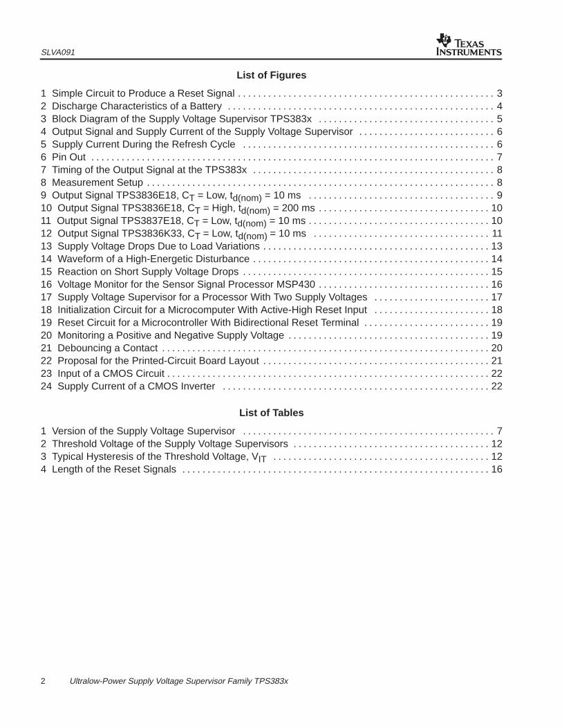
List of Figures
1 Simple Circuit to Produce a Reset Signal 3. . . . . . . . . . . . . . . . . . . . . . . . . . . . . . . . . . . . . . . . . . . . . . . . . . . 2 Discharge Characteristics of a Battery 4. . . . . . . . . . . . . . . . . . . . . . . . . . . . . . . . . . . . . . . . . . . . . . . . . . . . . 3 Block Diagram of the Supply Voltage Supervisor TPS383x 5. . . . . . . . . . . . . . . . . . . . . . . . . . . . . . . . . . . 4 Output Signal and Supply Current of the Supply Voltage Supervisor 6. . . . . . . . . . . . . . . . . . . . . . . . . . . 5 Supply Current During the Refresh Cycle 6. . . . . . . . . . . . . . . . . . . . . . . . . . . . . . . . . . . . . . . . . . . . . . . . . . 6 Pin Out 7. . . . . . . . . . . . . . . . . . . . . . . . . . . . . . . . . . . . . . . . . . . . . . . . . . . . . . . . . . . . . . . . . . . . . . . . . . . . . . . . 7 Timing of the Output Signal at the TPS383x 8. . . . . . . . . . . . . . . . . . . . . . . . . . . . . . . . . . . . . . . . . . . . . . . . 8 Measurement Setup 8. . . . . . . . . . . . . . . . . . . . . . . . . . . . . . . . . . . . . . . . . . . . . . . . . . . . . . . . . . . . . . . . . . . . . 9 Output Signal TPS3836E18, CT = Low, td(nom) = 10 ms 9. . . . . . . . . . . . . . . . . . . . . . . . . . . . . . . . . . . . . 10 Output Signal TPS3836E18, CT = High, td(nom) = 200 ms 10. . . . . . . . . . . . . . . . . . . . . . . . . . . . . . . . . . 11 Output Signal TPS3837E18, CT = Low, td(nom) = 10 ms 10. . . . . . . . . . . . . . . . . . . . . . . . . . . . . . . . . . . . 12 Output Signal TPS3836K33, CT = Low, td(nom) = 10 ms 11. . . . . . . . . . . . . . . . . . . . . . . . . . . . . . . . . . . 13 Supply Voltage Drops Due to Load Variations 13. . . . . . . . . . . . . . . . . . . . . . . . . . . . . . . . . . . . . . . . . . . . . 14 Waveform of a High-Energetic Disturbance 14. . . . . . . . . . . . . . . . . . . . . . . . . . . . . . . . . . . . . . . . . . . . . . . 15 Reaction on Short Supply Voltage Drops 15. . . . . . . . . . . . . . . . . . . . . . . . . . . . . . . . . . . . . . . . . . . . . . . . . 16 Voltage Monitor for the Sensor Signal Processor MSP430 16. . . . . . . . . . . . . . . . . . . . . . . . . . . . . . . . . . 17 Supply Voltage Supervisor for a Processor With Two Supply Voltages 17. . . . . . . . . . . . . . . . . . . . . . . 18 Initialization Circuit for a Microcomputer With Active-High Reset Input 18. . . . . . . . . . . . . . . . . . . . . . . 19 Reset Circuit for a Microcontroller With Bidirectional Reset Terminal 19. . . . . . . . . . . . . . . . . . . . . . . . . 20 Monitoring a Positive and Negative Supply Voltage 19. . . . . . . . . . . . . . . . . . . . . . . . . . . . . . . . . . . . . . . . 21 Debouncing a Contact 20. . . . . . . . . . . . . . . . . . . . . . . . . . . . . . . . . . . . . . . . . . . . . . . . . . . . . . . . . . . . . . . . . 22 Proposal for the Printed-Circuit Board Layout 21. . . . . . . . . . . . . . . . . . . . . . . . . . . . . . . . . . . . . . . . . . . . . 23 Input of a CMOS Circuit 22. . . . . . . . . . . . . . . . . . . . . . . . . . . . . . . . . . . . . . . . . . . . . . . . . . . . . . . . . . . . . . . . 24 Supply Current of a CMOS Inverter 22. . . . . . . . . . . . . . . . . . . . . . . . . . . . . . . . . . . . . . . . . . . . . . . . . . . . .
List of Tables
1 Version of the Supply Voltage Supervisor 7. . . . . . . . . . . . . . . . . . . . . . . . . . . . . . . . . . . . . . . . . . . . . . . . . . 2 Threshold Voltage of the Supply Voltage Supervisors 12. . . . . . . . . . . . . . . . . . . . . . . . . . . . . . . . . . . . . . . 3 Typical Hysteresis of the Threshold Voltage, VIT 12. . . . . . . . . . . . . . . . . . . . . . . . . . . . . . . . . . . . . . . . . . . 4 Length of the Reset Signals 16. . . . . . . . . . . . . . . . . . . . . . . . . . . . . . . . . . . . . . . . . . . . . . . . . . . . . . . . . . . . .
SLVA091
3 Ultralow-Power Supply Voltage Supervisor Family TPS383x
1 Introduction
Continuous advances in semiconductor-technology have led to more efficient integrated circuits.This is combined with a constant reduction of the circuit’s power dissipation, resulting in thedesign of equipment, that can be operated economically from a battery over a long period. Inmany cases, the designer only requests a function of the circuit if executing a current task, e.g.in a measurement recording system to sample and store a new date. Until a new measurementcan be taken, a certain time elapses in which the circuit can fall into a sleeping mode. In thismode, only basic functions are active, e.g. the clock generator, while the remaining parts of thesystem are placed in a low-power idle state. This technique is allowed in systems where theaverage current consumption is in the range of few microamperes only. Such an applicationdemands an extreme low-power dissipation of all integrated circuits in the system.
The supply voltage monitoring circuits that initialize the system also belong to the circuits. Thesedevices must be constantly active and are therefore highly responsible for a considerable part ofthe supply current.
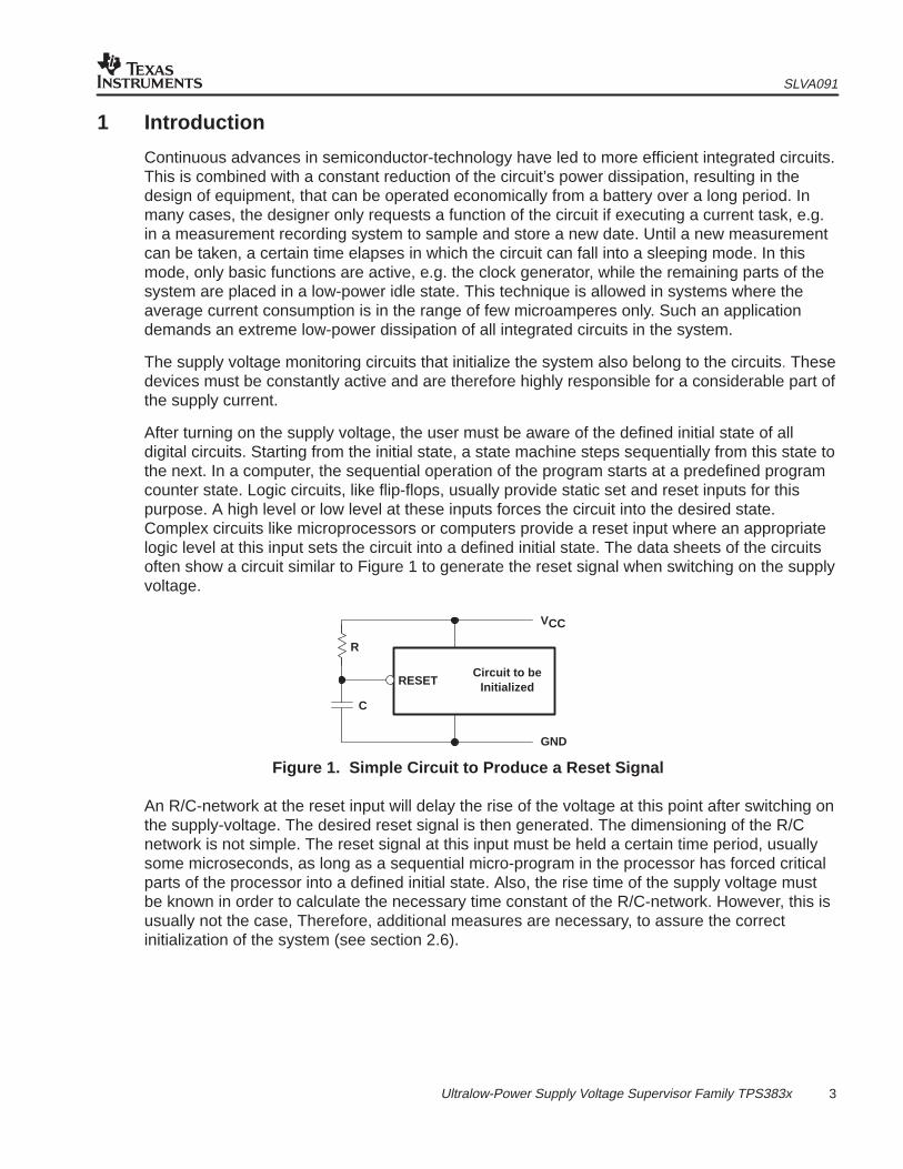
After turning on the supply voltage, the user must be aware of the defined initial state of alldigital circuits. Starting from the initial state, a state machine steps sequentially from this state tothe next. In a computer, the sequential operation of the program starts at a predefined programcounter state. Logic circuits, like flip-flops, usually provide static set and reset inputs for thispurpose. A high level or low level at these inputs forces the circuit into the desired state.Complex circuits like microprocessors or computers provide a reset input where an appropriatelogic level at this input sets the circuit into a defined initial state. The data sheets of the circuitsoften show a circuit similar to Figure 1 to generate the reset signal when switching on the supplyvoltage.
RESETCircuit to be
Initialized
R
C
VCC
GND
Figure 1. Simple Circuit to Produce a Reset Signal
An R/C-network at the reset input will delay the rise of the voltage at this point after switching onthe supply-voltage. The desired reset signal is then generated. The dimensioning of the R/Cnetwork is not simple. The reset signal at this input must be held a certain time period, usuallysome microseconds, as long as a sequential micro-program in the processor has forced criticalparts of the processor into a defined initial state. Also, the rise time of the supply voltage mustbe known in order to calculate the necessary time constant of the R/C-network. However, this isusually not the case, Therefore, additional measures are necessary, to assure the correctinitialization of the system (see section 2.6).
SLVA091
4 Ultralow-Power Supply Voltage Supervisor Family TPS383x
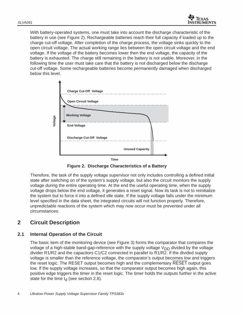
With battery-operated systems, one must take into account the discharge characteristic of thebattery in use (see Figure 2). Rechargeable batteries reach their full capacity if loaded up to thecharge cut-off voltage. After completion of the charge process, the voltage sinks quickly to theopen circuit voltage. The actual working range lies between the open circuit voltage and the endvoltage. If the voltage of the battery becomes lower then the end voltage, the capacity of thebattery is exhausted. The charge still remaining in the battery is not usable. Moreover, in thefollowing time the user must take care that the battery is not discharged below the dischargecut-off voltage. Some rechargeable batteries become permanently damaged when dischargedbelow this level.
Working Voltage
Vol
tage
Open Circuit Voltage
End Voltage
Discharge Cut-Off Voltage
Unused Capacity
Time
Charge Cut-Off Voltage
Figure 2. Discharge Characteristics of a Battery
Therefore, the task of the supply voltage supervisor not only includes controlling a defined initialstate after switching on of the system’s supply voltage, but also the circuit monitors the supplyvoltage during the entire operating time. At the end the useful operating time, when the supplyvoltage drops below the end voltage, it generates a reset signal. Now its task is not to reinitializethe system but to force it into a defined idle state. If the supply voltage falls under the minimumlevel specified in the data sheet, the integrated circuits will not function properly. Therefore,unpredictable reactions of the system which may now occur must be prevented under allcircumstances.
2 Circuit Description
2.1 Internal Operation of the Circuit
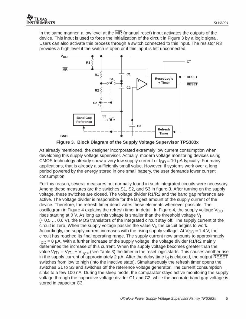
The basic item of the monitoring device (see Figure 3) forms the comparator that compares thevoltage of a high-stable band-gap-reference with the supply voltage VDD divided by the voltagedivider R1/R2 and the capacitors C1/C2 connected in parallel to R1/R2. If the divided supplyvoltage is smaller than the reference voltage, the comparator’s output becomes low and triggersthe reset logic. The RESET output becomes high and the complementary RESET output goeslow. If the supply voltage increases, so that the comparator output becomes high again, thispositive edge triggers the timer in the reset logic. The timer holds the outputs further in the activestate for the time td (see section 2.6).
SLVA091
5 Ultralow-Power Supply Voltage Supervisor Family TPS383x
In the same manner, a low level at the MR (manual reset) input activates the outputs of thedevice. This input is used to force the initialization of the circuit in Figure 3 by a logic signal.Users can also activate this process through a switch connected to this input. The resistor R3provides a high level if the switch is open or if this input is left unconnected.
_+
Reset Logic+ Timer
C1
C2
R1S1
R2
Band GapReference
RefreshTimer
S2
S3
R3 CT
RESET
RESET
C3
VDD
MR
GND
Figure 3. Block Diagram of the Supply Voltage Supervisor TPS383x
As already mentioned, the designer incorporated extremely low current consumption whendeveloping this supply voltage supervisor. Actually, modern voltage monitoring devices usingCMOS technology already show a very low supply current of IDD = 10 µA typically. For manyapplications, that is already a sufficiently small value. However, if systems work over a longperiod powered by the energy stored in one small battery, the user demands lower currentconsumption.
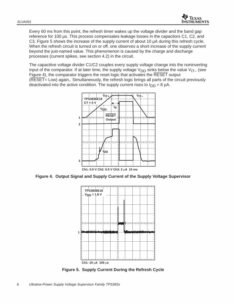
For this reason, several measures not normally found in such integrated circuits were necessary.Among these measures are the switches S1, S2, and S3 in figure 3. After turning on the supplyvoltage, these switches are closed. The voltage divider R1/R2 and the band gap reference areactive. The voltage divider is responsible for the largest amount of the supply current of thedevice. Therefore, the refresh timer deactivates these elements whenever possible. Theoscillogram in Figure 4 explains the refresh timer in detail. In Figure 4, the supply voltage VDDrises starting at 0 V. As long as this voltage is smaller than the threshold voltage Vt(≈ 0.5 … 0.6 V), the MOS transistors of the integrated circuit stay off. The supply current of thecircuit is zero. When the supply voltage passes the value Vt, the circuit begins to work.Accordingly, the supply current increases with the rising supply voltage. At VDD ≈ 1.4 V, thecircuit has reached its final operating range. The supply current now amounts to approximatelyIDD = 8 µA. With a further increase of the supply voltage, the voltage divider R1/R2 mainlydetermines the increase of this current. When the supply voltage becomes greater than thevalue VIT+ = VIT– + Vhys, (see Table 3) the timer in the reset logic starts. This causes another risein the supply current of approximately 2 µA. After the delay time td is elapsed, the output RESETswitches from low to high (into the inactive state). Simultaneously the refresh timer opens theswitches S1 to S3 and switches off the reference voltage generator. The current consumptionsinks to a few 100 nA. During the sleep mode, the comparator stays active monitoring the supplyvoltage through the capacitive voltage divider C1 and C2, while the accurate band gap voltage isstored in capacitor C3.
SLVA091
6 Ultralow-Power Supply Voltage Supervisor Family TPS383x
Every 60 ms from this point, the refresh timer wakes up the voltage divider and the band gapreference for 100 µs. This process compensates leakage losses in the capacitors C1, C2, andC3. Figure 5 shows the increase of the supply current of about 10 µA during this refresh cycle.When the refresh circuit is turned on or off, one observes a short increase of the supply currentbeyond the just-named value. This phenomenon is caused by the charge and dischargeprocesses (current spikes, see section 4.2) in the circuit.
The capacitive voltage divider C1/C2 couples every supply voltage change into the noninvertinginput of the comparator. If at later time, the supply voltage VDD sinks below the value VIT– (seeFigure 4), the comparator triggers the reset logic that activates the RESET output (RESET= Low) again,. Simultaneously, the refresh logic brings all parts of the circuit previouslydeactivated into the active condition. The supply current rises to IDD = 8 µA.
1
3
2
Ch1: 0.5 V Ch2: 0.5 V Ch3: 2 µA 10 ms
TPS3836E18CT = 0 V
VIT+ VIT–
VDD
RESETOutput
IDD
td
Figure 4. Output Signal and Supply Current of the Supply Voltage Supervisor
1
TPS3836E18VDD = 1.8 V
Ch1: 10 µA 100 µs
Figure 5. Supply Current During the Refresh Cycle
SLVA091
7 Ultralow-Power Supply Voltage Supervisor Family TPS383x
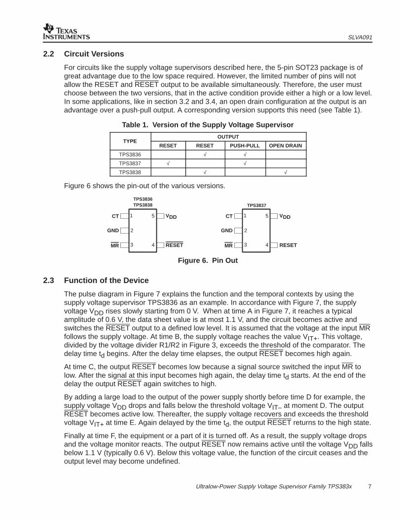
2.2 Circuit Versions
For circuits like the supply voltage supervisors described here, the 5-pin SOT23 package is ofgreat advantage due to the low space required. However, the limited number of pins will notallow the RESET and RESET output to be available simultaneously. Therefore, the user mustchoose between the two versions, that in the active condition provide either a high or a low level.In some applications, like in section 3.2 and 3.4, an open drain configuration at the output is anadvantage over a push-pull output. A corresponding version supports this need (see Table 1).
Table 1. Version of the Supply Voltage Supervisor
TYPEOUTPUT
TYPERESET RESET PUSH-PULL OPEN DRAIN
TPS3836 √ √
TPS3837 √ √
TPS3838 √ √
Figure 6 shows the pin-out of the various versions.
3
2
4
51
TPS3836TPS3838
CT
GND
MR
VDD
RESET 3
2
4
51
TPS3837
CT
GND
MR
VDD
RESET
Figure 6. Pin Out
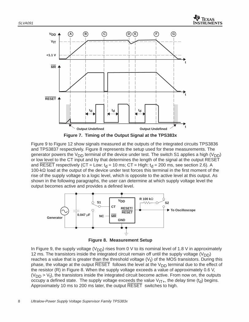
2.3 Function of the Device
The pulse diagram in Figure 7 explains the function and the temporal contexts by using thesupply voltage supervisor TPS3836 as an example. In accordance with Figure 7, the supplyvoltage VDD rises slowly starting from 0 V. When at time A in Figure 7, it reaches a typicalamplitude of 0.6 V, the data sheet value is at most 1.1 V, and the circuit becomes active andswitches the RESET output to a defined low level. It is assumed that the voltage at the input MRfollows the supply voltage. At time B, the supply voltage reaches the value VIT+. This voltage,divided by the voltage divider R1/R2 in Figure 3, exceeds the threshold of the comparator. Thedelay time td begins. After the delay time elapses, the output RESET becomes high again.
At time C, the output RESET becomes low because a signal source switched the input MR tolow. After the signal at this input becomes high again, the delay time td starts. At the end of thedelay the output RESET again switches to high.
By adding a large load to the output of the power supply shortly before time D for example, thesupply voltage VDD drops and falls below the threshold voltage VIT– at moment D. The outputRESET becomes active low. Thereafter, the supply voltage recovers and exceeds the thresholdvoltage VIT+ at time E. Again delayed by the time td, the output RESET returns to the high state.
Finally at time F, the equipment or a part of it is turned off. As a result, the supply voltage dropsand the voltage monitor reacts. The output RESET now remains active until the voltage VDD fallsbelow 1.1 V (typically 0.6 V). Below this voltage value, the function of the circuit ceases and theoutput level may become undefined.
SLVA091
8 Ultralow-Power Supply Voltage Supervisor Family TPS383x
td td td
t
t
t
A B C D E F G
Output Undefined Output Undefined
VDD
VIT
<1.1 V
MR
RESET
Figure 7. Timing of the Output Signal at the TPS383x
Figure 9 to Figure 12 show signals measured at the outputs of the integrated circuits TPS3836and TPS3837 respectively. Figure 8 represents the setup used for these measurements. Thegenerator powers the VDD terminal of the device under test. The switch S1 applies a high (VDD)or low level to the CT input and by that determines the length of the signal at the output RESETand RESET respectively (CT = Low: td = 10 ms; CT = High: td = 200 ms, see section 2.6). A100-kΩ load at the output of the device under test forces this terminal in the first moment of therise of the supply voltage to a logic level, which is opposite to the active level at this output. Asshown in the following paragraphs, the user can determine at which supply voltage level theoutput becomes active and provides a defined level.
VDD
CT
GNDMR
RESET/RESET
0.047 µF
S1
NC
R 100 kΩS2
Generator
To Oscilloscope
Figure 8. Measurement Setup
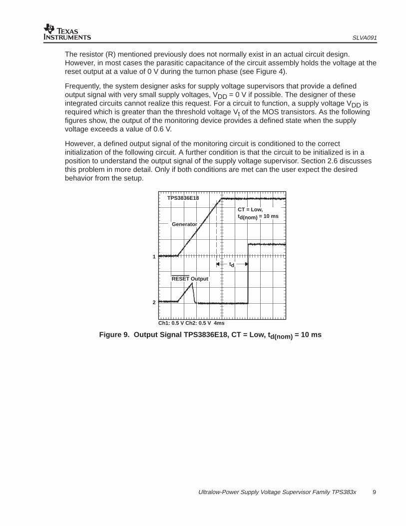
In Figure 9, the supply voltage (VDD) rises from 0 V to its nominal level of 1.8 V in approximately12 ms. The transistors inside the integrated circuit remain off until the supply voltage (VDD)reaches a value that is greater than the threshold voltage (Vt) of the MOS transistors. During thisphase, the voltage at the output RESET follows the level at the VDD terminal due to the effect ofthe resistor (R) in Figure 8. When the supply voltage exceeds a value of approximately 0.6 V,(VDD > Vt), the transistors inside the integrated circuit become active. From now on, the outputsoccupy a defined state. The supply voltage exceeds the value VIT+, the delay time (td) begins.Approximately 10 ms to 200 ms later, the output RESET switches to high.
SLVA091
9 Ultralow-Power Supply Voltage Supervisor Family TPS383x
The resistor (R) mentioned previously does not normally exist in an actual circuit design.However, in most cases the parasitic capacitance of the circuit assembly holds the voltage at thereset output at a value of 0 V during the turnon phase (see Figure 4).
Frequently, the system designer asks for supply voltage supervisors that provide a definedoutput signal with very small supply voltages, VDD = 0 V if possible. The designer of theseintegrated circuits cannot realize this request. For a circuit to function, a supply voltage VDD isrequired which is greater than the threshold voltage Vt of the MOS transistors. As the followingfigures show, the output of the monitoring device provides a defined state when the supplyvoltage exceeds a value of 0.6 V.
However, a defined output signal of the monitoring circuit is conditioned to the correctinitialization of the following circuit. A further condition is that the circuit to be initialized is in aposition to understand the output signal of the supply voltage supervisor. Section 2.6 discussesthis problem in more detail. Only if both conditions are met can the user expect the desiredbehavior from the setup.
1
2
TPS3836E18
Generator
td
RESET Output
Ch1: 0.5 V Ch2: 0.5 V 4ms
CT = Low,td(nom) = 10 ms
Figure 9. Output Signal TPS3836E18, CT = Low, t d(nom) = 10 ms
SLVA091
10 Ultralow-Power Supply Voltage Supervisor Family TPS383x
1
2
TPS3836E18Generator
RESET Output
Ch1: 0.5 V Ch2: 0.5 V 40 ms
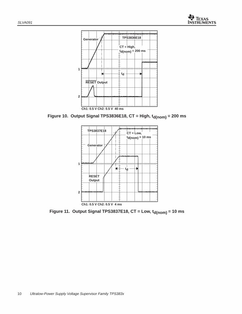
CT = High,td(nom) = 200 ms
td
Figure 10. Output Signal TPS3836E18, CT = High, t d(nom) = 200 ms
2
TPS3837E18
Generator
RESETOutput
Ch1: 0.5 V Ch2: 0.5 V 4 ms
CT = Low,td(nom) = 10 ms
td
1
Figure 11. Output Signal TPS3837E18, CT = Low, t d(nom) = 10 ms

SLVA091
11 Ultralow-Power Supply Voltage Supervisor Family TPS383x
1
2
TPS3836K33
Generator
RESET Output
Ch1: 1 V Ch2: 1 V 4 ms
CT = Low,td(nom) = 10 ms
td
Figure 12. Output Signal TPS3836K33, CT = Low, t d(nom) = 10 ms
2.4 Threshold Voltage of the Supply Voltage Supervisor
The supply voltage supervisors described here display the proper operation of the power supply.Primarily of interest is a drop in this voltage, where the supply voltage falls under the minimumvalue required for a proper operation of the circuit. In the data sheets of the integrated circuits,this minimum value is designated: VCC(min) or VDD(min). This value takes the most unfavorableoperating conditions into account:
• Process related deviations of the transistor parameters to the unfavorable side: with MOStransistors a high on-resistor, with bipolar transistors a low current gain.
• Unfavorable ambient temperature for the respective circuit: with MOS transistors a highvalue, that causes a high on-resistor of the device, with bipolar transistors a lowtemperature, that has a low current gain as the consequence.
• Highest possible clock frequency of the circuit, which presupposes the optimum performanceof the transistors.
Under these conditions, the data sheets specify a minimum operating voltage that, with logiccircuits, lies 10% below the nominal value. Complex MOS circuits, like microprocessors,demand a supply voltage that falls below the nominal value by no more than 5%. However, a10% undervoltage can usually be tolerated in these cases. In rare cases, all of the mentionedoperating parameters are the worst case. Mindful of these considerations, supply voltagesupervisors where the threshold voltage (VIT–) lies 10% below the nominal supply voltage areoffered.
Based on these points of view, the threshold voltages (VIT–) of the integrated circuits of theseries TPS383x were selected (see Table 2).
SLVA091
12 Ultralow-Power Supply Voltage Supervisor Family TPS383x
Table 2. Threshold Voltage of the Supply Voltage Supervisors
TYPENOMINAL SUPPLY
VOLTAGE VDD
THRESHOLD VOLTAGEVIT–
UNDERVOLTAGE %
TPS383xE18 1.8 V 1.71 V 5
TPS383xJ25 2.5 V 2.25 V 10
TPS383xL30 3.0 V 2.64 V 12
TPS383xK33 3.3 V 2.93 V 11
In order to prevent a consecutive and repeated response of the monitor circuit with low periodicfluctuations of the supply voltage (VDD), the comparator has a hysteresis of a few millivolts (seeTable 3). In practice, the low-pass characteristic produced by the delay circuit following thecomparator will probably prevent a repeated reaction of the device under the just-mentionedcircumstances. In this case, the output is held continuously active by the consecutive retrigger ofthe reset timer.
Table 3. Typical Hysteresis of the Threshold Voltage, V IT
NOMINAL THRESHOLDVOLTAGE VIT–
TYPICAL HYSTERESISVhys
1.7 V < VIT– < 2.5 V 30 mV
2.5 V < VIT– < 3.5 V 40 mV
3.5 V < VIT– < 5.0 V 50 mV
2.5 Length of the Reset Signals
The integrated circuits described here will recognize voltage drops of the supply voltage that canendanger the reliable operation of the circuit. To assess the amplitude and duration of thesevoltage drops and to judge the effectiveness of the monitoring device, the user must analyze thecause. Voltage drops of the supply voltage have two essential causes:
• Extreme load variations that cannot be stabilized by the voltage regulator sufficiently orquickly or cannot be stabilized at all.
• Voltages that are coupled from external noise sources into the system. These disturbancescome from electrostatic discharges, arcs, inductive loads, and sometimes lightning impactsduring a thunderstorm. They sometimes distinguish themselves through extremely highenergies.
2.5.1 Supply Voltage Drops Due to Load Variations
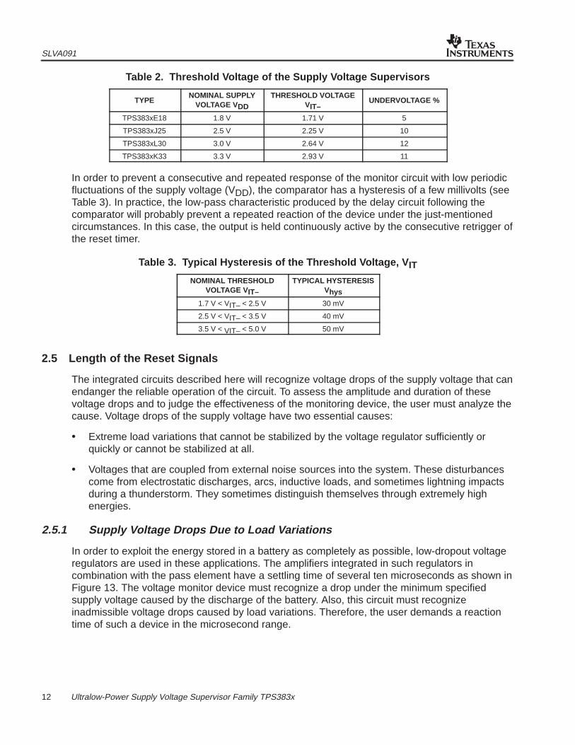
In order to exploit the energy stored in a battery as completely as possible, low-dropout voltageregulators are used in these applications. The amplifiers integrated in such regulators incombination with the pass element have a settling time of several ten microseconds as shown inFigure 13. The voltage monitor device must recognize a drop under the minimum specifiedsupply voltage caused by the discharge of the battery. Also, this circuit must recognizeinadmissible voltage drops caused by load variations. Therefore, the user demands a reactiontime of such a device in the microsecond range.
SLVA091
13 Ultralow-Power Supply Voltage Supervisor Family TPS383x
–100
0.5
0
0 604020 80 100 140120 160 180 200
1
–50
0
50
100TPS76733CL = 100 µFϑA = 25°C
– O
utpu
t Cur
rent
– A
Out
put V
olta
ge –
mV
I O
– V
aria
tion
of th
eV
O∆
t – Time – µs
Figure 13. Supply Voltage Drops Due to Load Variations
2.5.2 Influence the Supply Voltage Through External Noise Sources
The estimation of the consequences of disturbances that comes from external noise sources ismore difficult. Such sources could be:
• Electrostatic discharges have an amplitude of several thousand volts. Due to the limitedamount of energy in the discharge, e.g. the energy stored in a human body, such dischargeslast only a few nanoseconds. Admittedly, the amplitude of the discharge is very high. Theinductance of the interconnects quickly damps the wave propagating from the point ofdischarge. Even if the discharge is very dangerous for the integrated circuits, it isquestionable whether a signal is sufficient enough to appear at the sense input of the supplyvoltage supervisor.
• The user has to consider that the application area of the monitor device described here ismainly in battery-operated equipment. With these applications, the user can assume in manycases that the monitored circuit has no galvanic connection to the outside world. With asufficient isolation of the equipment against an unintentional touch of sensitive components,one can prevent high currents flowing through critical parts of the system.
• Lightning is among the electrostatic discharges. The duration of such discharges is so bigthat monitoring circuits can recognize the resulting supply voltage drops. Experienceteaches, however, that the induced energy may be so high that it probably will destroy thecircuit.
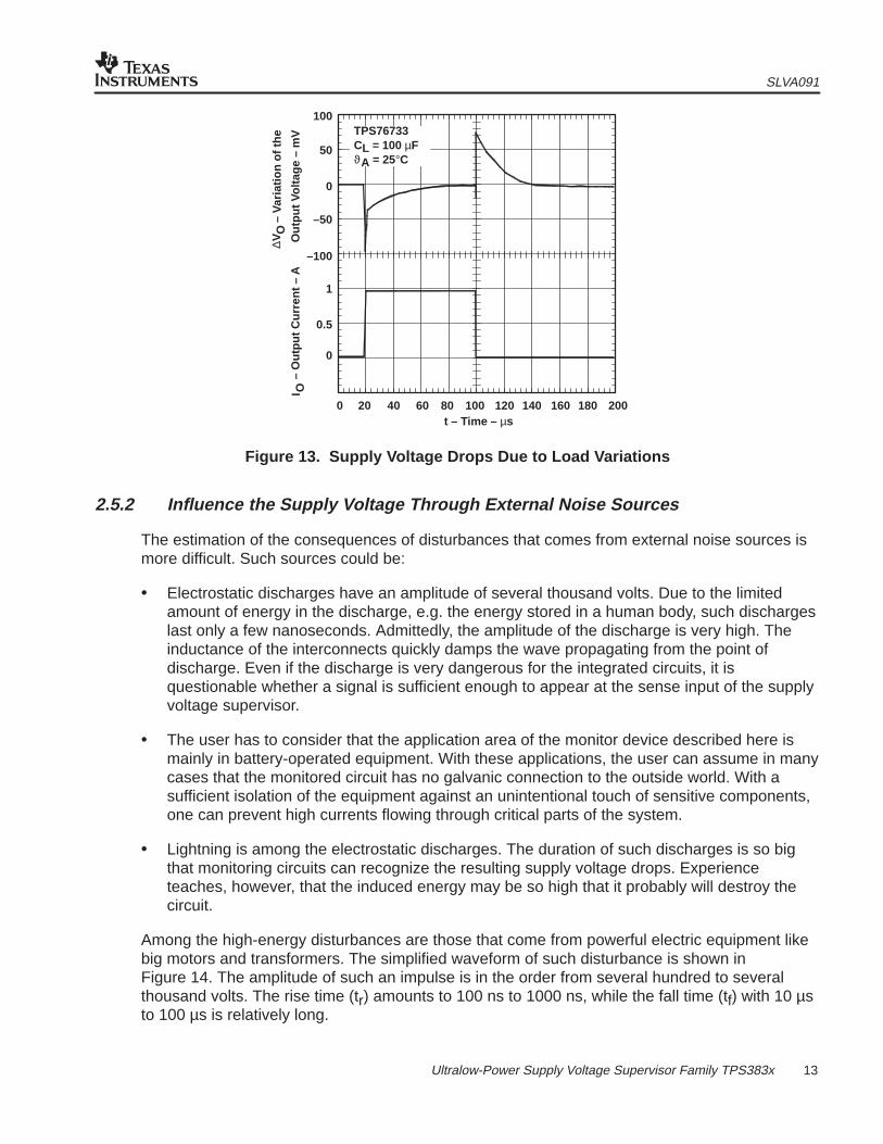
Among the high-energy disturbances are those that come from powerful electric equipment likebig motors and transformers. The simplified waveform of such disturbance is shown in Figure 14. The amplitude of such an impulse is in the order from several hundred to severalthousand volts. The rise time (tr) amounts to 100 ns to 1000 ns, while the fall time (tf) with 10 µsto 100 µs is relatively long.
SLVA091
14 Ultralow-Power Supply Voltage Supervisor Family TPS383x
tf t
V
tr
Figure 14. Waveform of a High-Energetic Disturbance
The coupling path between noise sources and noise destination influences the actual effectiveform and amplitude of the impulse. In practice, the user must calculate a pulse-width in themicrosecond range with insufficient decoupling or poor shielding.
Concerning the possible influence of these disturbances on battery-operated equipment, it isvalid to refer to the preceding text on electrostatic discharges. As long as the circuit does nothave any electric connection to the outside world, the previously mentioned disturbances willhave no influence on the function of the appliance. However, any electric connection to theoutside world represents a probable noise path. This is also valid for galvanic isolatedconnections. The inherent existing stray capacitance of the interface is a possible path for thedisturbing signals.
2.5.3 Behavior of the Supply Voltage Supervisor TPS383x
Supply voltage supervisors will recognize a deviation in the supply voltage from its nominalvalue and generate a signal when the voltage falls below the minimum acceptable value. Theseprocesses take place in the millisecond range. It is also necessary to recognize externaldisturbances, which influence the voltage supply, and to force a reinitialization of the system ifrequired. In this case the monitoring circuit must recognize deviations in the microsecond range.
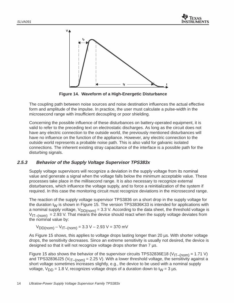
The reaction of the supply voltage supervisor TPS3836 on a short drop in the supply voltage forthe duration tW is shown in Figure 15. The version TPS3836K33 is intended for applications witha nominal supply voltage, VDD(nom) = 3.3 V. According to the data sheet, the threshold voltage isVIT–(nom) = 2.93 V. That means the device should react when the supply voltage deviates fromthe nominal value by:
VDD(nom) – VIT–(nom) = 3.3 V – 2.93 V = 370 mV
As Figure 15 shows, this applies to voltage drops lasting longer than 20 µs. With shorter voltagedrops, the sensitivity decreases. Since an extreme sensitivity is usually not desired, the device isdesigned so that it will not recognize voltage drops shorter than 7 µs.
Figure 15 also shows the behavior of the supervisor circuits TPS32836E18 (VIT–(nom) = 1.71 V)and TPS32836J25 (VIT–(nom) = 2.25 V). With a lower threshold voltage, the sensitivity against ashort voltage sometimes increases slightly, e.g., the device to be used with a nominal supplyvoltage, VDD = 1.8 V, recognizes voltage drops of a duration down to tW = 3 µs.
SLVA091
15 Ultralow-Power Supply Voltage Supervisor Family TPS383x
TPS3836K33
TPS3836J25TPS3836E18
1
0.8
0.4
0
Vol
tage
Dro
p –
1.2
1.4
1.6
0.6
0.2
0 µs 10 µs 20 µs 30 µs 40 µs 50 µsPulse Width – t w
V∆
Figure 15. Reaction on Short Supply Voltage Drops
2.6 Length of the Reset Signals
One of the essential tasks of the supply voltage supervisors is to assure a correct initialization ofthe system. Integrated circuits require a reset signal of a specified length at its reset input. Withlogic circuits, this signal duration is in the range of a few nanoseconds. Complex integratedcircuits like microprocessors execute during the initialization of a microprogram that brings theindividual parts of the circuit sequentially into the desired state. The following conditions must befulfilled in order to assure a correct result:
• The supply voltage must have risen at least to the voltage VDD(min), and VCC(min)respectively to assure the correct function of the total circuit.
• The clock generator (oscillator) of the circuit to be initialized must work correctly in order toassure the execution of the microprogram.
• The reset signal must last until the successful completion of the initialization.
The comparator in the supply voltage supervisor recognizes the achievement of a sufficientsupply voltage, point B in Figure 7. The execution of the microprogram lasts approximately100 ns up to a few microseconds; the exact value is found in the data sheet of thecorresponding circuit. Essentially, it often lasts until the oscillator of the circuit works correctly.Clock generators are usually crystal-controlled. Crystals are components with a very high quality(Q > 104). With the correct dimensioning of this circuit, the settling time of the oscillator lasts upto several ten milliseconds (see section 3.1). For this reason, the delay time (td) of thesupervision circuits normally amounts to approximately 100 ms. With the integrated circuit of theseries TPS383x discussed here, this value amounts to td(typ) = 200 ms.
SLVA091
16 Ultralow-Power Supply Voltage Supervisor Family TPS383x
Many applications ask for a real-time clock that runs in the standby mode. Due to cost andperformance reasons, the frequency of these oscillators is mainly controlled by watch crystals(f = 32.768 kHz). For cost reasons, this signal serves as a time base for the clock generator ofthe processor itself. It is a voltage-controlled ring-oscillator in which frequency is controlled via aphase-lock loop (PLL) to the multiple frequencies of the watch crystal. These ring-oscillatorshave a settling time of a few periods only. After this time the processor is able to function even ifthe frequency is not correct until the final settling of the PLL. Under such circumstances, theuser can shorten the length of the reset signals.
With the supervision circuit of the TPS383x, the user has the ability to select the appropriatedelay time via a corresponding logic level at the CT input (see Table 4).
Table 4. Length of the Reset Signals
INPUT CTLENGTH OF THERESET SIGNALS
High 200 ms
Low 10 ms
3 Application Examples
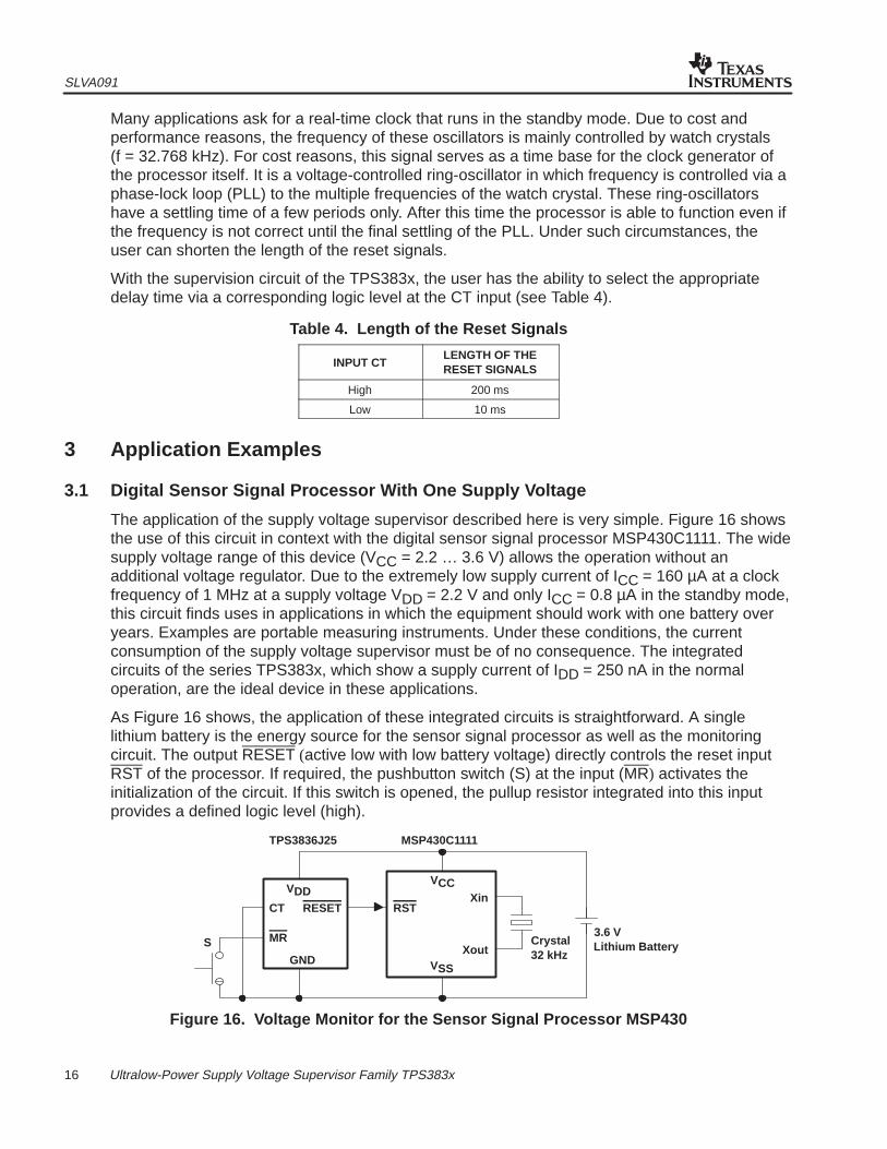
3.1 Digital Sensor Signal Processor With One Supply Voltage
The application of the supply voltage supervisor described here is very simple. Figure 16 showsthe use of this circuit in context with the digital sensor signal processor MSP430C1111. The widesupply voltage range of this device (VCC = 2.2 … 3.6 V) allows the operation without anadditional voltage regulator. Due to the extremely low supply current of ICC = 160 µA at a clockfrequency of 1 MHz at a supply voltage VDD = 2.2 V and only ICC = 0.8 µA in the standby mode,this circuit finds uses in applications in which the equipment should work with one battery overyears. Examples are portable measuring instruments. Under these conditions, the currentconsumption of the supply voltage supervisor must be of no consequence. The integratedcircuits of the series TPS383x, which show a supply current of IDD = 250 nA in the normaloperation, are the ideal device in these applications.
As Figure 16 shows, the application of these integrated circuits is straightforward. A singlelithium battery is the energy source for the sensor signal processor as well as the monitoringcircuit. The output RESET (active low with low battery voltage) directly controls the reset inputRST of the processor. If required, the pushbutton switch (S) at the input (MR) activates theinitialization of the circuit. If this switch is opened, the pullup resistor integrated into this inputprovides a defined logic level (high).
VDDCT
MR
GND
RESET
S
VCC
RST
VSS
Xin
XoutCrystal32 kHz
3.6 VLithium Battery
TPS3836J25 MSP430C1111
Figure 16. Voltage Monitor for the Sensor Signal Processor MSP430
SLVA091
17 Ultralow-Power Supply Voltage Supervisor Family TPS383x
The logic level at the entrance CT of the supply voltage supervisor determines the length of thereset signals. The clock generator of the signal processor consists of a programmable ringoscillator, the frequency of which may be set to f = 1 MHz. The crystal serves as the time basisfor the integrated real-time clock and supports the extremely low current consumption of theprocessor in the standby mode (clock generator turned off). The ring oscillator in the clockgenerator, which controls the operations of the processor, has a settling time that lasts only fewperiods of this oscillator. Accordingly the user can choose the delay time of the supply voltagesupervisor. For this reason, in Figure 16, a low level is applied to the CT input. This yields adelay time td = 10 ms (see Table 4).
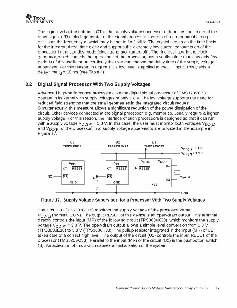
3.2 Digital Signal Processor With Two Supply Voltages
Advanced high-performance processors like the digital signal processor of TMS320VC33operate in its kernel with supply voltages of only 1.8 V. The low voltage supports the need forreduced field strengths that the small geometries in the integrated circuit request.Simultaneously, this measure allows a significant reduction of the power dissipation of thecircuit. Other devices connected at the signal processor, e.g. memories, usually require a highersupply voltage. For this reason, the interface of such processors is designed so that it can runwith a supply voltage VDD(P) = 3.3 V. In this case, the user must monitor both voltages VDD(L)and VDD(P) of the processor. Two supply voltage supervisors are provided in the example inFigure 17.
VDDCT
MR
GND
RESET
NC
VDDL
RESET
VSS
X1
X2Crystal
U1TPS3838E18
VDDCT
MR
GND
RESET
S
VDDP
U2TPS38386K33
U3TMS320VC33
VDD(L) = 1.8 V
VDD(P) = 3.3 V
GND
Figure 17. Supply Voltage Supervisor for a Processor With Two Supply Voltages
The circuit U1 (TPS3838E18) monitors the supply voltage of the processor kernelVDD(L) (nominal 1.8 V). The output RESET of this device is an open-drain output. This terminaldirectly controls the input (MR) of the following circuit (TPS3836K33), which monitors the supplyvoltage VDD(P) = 3.3 V. The open-drain output allows a simple level conversion from 1.8 V(TPS3838E18) to 3.3 V (TPS3836K33). The pullup resistor integrated in the input (MR) of U2takes care of a correct high level. The output of the circuit (U2) controls the input RESET of theprocessor (TMS320VC33). Parallel to the input (MR) of the circuit (U2) is the pushbotton switch(S). An activation of this switch causes an initialization of the system.
SLVA091
18 Ultralow-Power Supply Voltage Supervisor Family TPS383x
Finally, the logic levels at the inputs (CT) have to be determined. The logic levels determine thelength of the reset signals. The processor (TMS320VC33) has an integrated crystal oscillator(terminals X1 and X2). For the correct initialization of the processor, a sufficient amplitude of theoscillator voltage is necessary. As mentioned in section 2.6, the settling time of correctlydimensioned crystal oscillators last several 10 milliseconds. Therefore, the user chooses a valueof 200 ms as the reset time of the circuit, U2 (CT = high). Now the only task of the circuit (U1) isto monitor the supply voltage VDD(L). In principle a simple comparator function would besufficient for this task. A timing extension of the reset signals is not necessary. Therefore, a lowlevel at the input (CT) of this circuit selects the shorter of the two delay times.
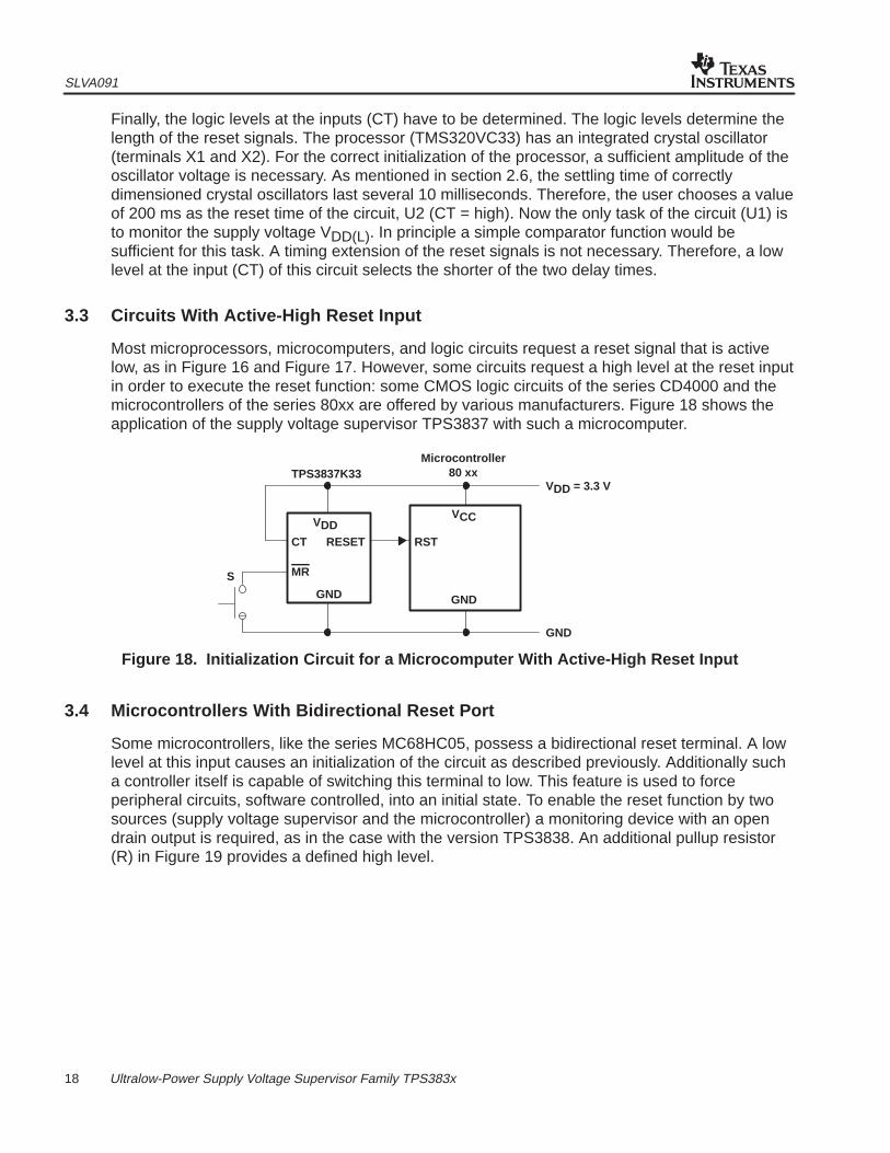
3.3 Circuits With Active-High Reset Input
Most microprocessors, microcomputers, and logic circuits request a reset signal that is activelow, as in Figure 16 and Figure 17. However, some circuits request a high level at the reset inputin order to execute the reset function: some CMOS logic circuits of the series CD4000 and themicrocontrollers of the series 80xx are offered by various manufacturers. Figure 18 shows theapplication of the supply voltage supervisor TPS3837 with such a microcomputer.
VDDCT
MR
GND
RESET
S
VCC
RST
GND
TPS3837K33Microcontroller
80 xxVDD = 3.3 V
GND
Figure 18. Initialization Circuit for a Microcomputer With Active-High Reset Input
3.4 Microcontrollers With Bidirectional Reset Port
Some microcontrollers, like the series MC68HC05, possess a bidirectional reset terminal. A lowlevel at this input causes an initialization of the circuit as described previously. Additionally sucha controller itself is capable of switching this terminal to low. This feature is used to forceperipheral circuits, software controlled, into an initial state. To enable the reset function by twosources (supply voltage supervisor and the microcontroller) a monitoring device with an opendrain output is required, as in the case with the version TPS3838. An additional pullup resistor(R) in Figure 19 provides a defined high level.
SLVA091
19 Ultralow-Power Supply Voltage Supervisor Family TPS383x
VDDCT
MR
GND
RESET
TPS3838K33
S
MicrocontrollerMC68HC05
PeripheralCircuit
VDD = 3.3 V
GND
RESET
GND
VDD
R10 kΩ
RESET
VDD
GND
Figure 19. Reset Circuit for a Microcontroller With Bidirectional Reset Terminal
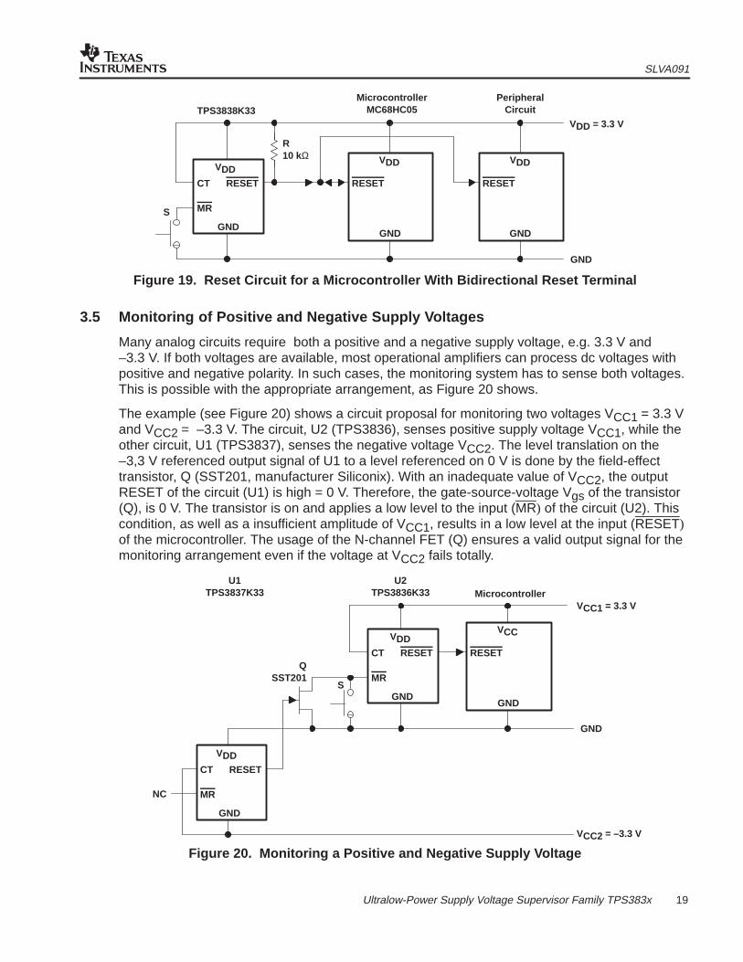
3.5 Monitoring of Positive and Negative Supply Voltages
Many analog circuits require both a positive and a negative supply voltage, e.g. 3.3 V and–3.3 V. If both voltages are available, most operational amplifiers can process dc voltages withpositive and negative polarity. In such cases, the monitoring system has to sense both voltages.This is possible with the appropriate arrangement, as Figure 20 shows.
The example (see Figure 20) shows a circuit proposal for monitoring two voltages VCC1 = 3.3 Vand VCC2 = –3.3 V. The circuit, U2 (TPS3836), senses positive supply voltage VCC1, while theother circuit, U1 (TPS3837), senses the negative voltage VCC2. The level translation on the–3,3 V referenced output signal of U1 to a level referenced on 0 V is done by the field-effecttransistor, Q (SST201, manufacturer Siliconix). With an inadequate value of VCC2, the outputRESET of the circuit (U1) is high = 0 V. Therefore, the gate-source-voltage Vgs of the transistor(Q), is 0 V. The transistor is on and applies a low level to the input (MR) of the circuit (U2). Thiscondition, as well as a insufficient amplitude of VCC1, results in a low level at the input (RESET)of the microcontroller. The usage of the N-channel FET (Q) ensures a valid output signal for themonitoring arrangement even if the voltage at VCC2 fails totally.
VDDCT
MR
GND
RESET
U2TPS3836K33
S
MicrocontrollerVCC1 = 3.3 V
GND
RESET
GND
VCC
VDDCT
MR
GND
RESET
NC
VCC2 = –3.3 V
U1TPS3837K33
QSST201
Figure 20. Monitoring a Positive and Negative Supply Voltage

SLVA091
20 Ultralow-Power Supply Voltage Supervisor Family TPS383x
3.6 Debouncing of Switches
Other applications can use supply voltage supervisors. A frequently occurring problem is thedebouncing of mechanical contacts. If the contact surface clashes with the closing of thecontact, it bounces back several times. A similar effect is observed later when opening thecontact. According to the construction of the contact, this bounce period lasts in the range fromhundreds of microseconds to tens of milliseconds. In the comparison to the reaction speed ofdigital circuits, it is a very long period, so the bouncing of the contact is interpreted as multipleevents.
VDDCT
MR
GND
RESET
S
TPS3836E18
VDD
GND
Contact Bouncingat Opening Switch
Contact Bouncingat Closing Switch
RESETOutput
td
Figure 21. Debouncing a Contact
A known circuit arrangement to debounce a contact consists of a low-pass filter followed by aSchmitt-trigger. These functions comprise the supervisor circuits. When activating thepushbutton switch (S) in Figure 21, the input (MR) becomes low. The output (RESET) followsthis signal. The low level at the input simultaneously activates the reset timer (see Figure 7) thatkeeps the output, an additional 200 ms, in the active mode after a positive edge at the input(MR). This provides the low-pass characteristic that fades multiple pulses caused by thebouncing contact. The same happens when opening the contact. When selecting a suitableintegrated circuit for debounce purposes, the user has to look for a device whose thresholdvoltage (VIT–) is much lower than the minimum supply voltage of the system. Therefore, a circuitwith a threshold voltage of VIT– = 1.71 V is used in this example with a supply voltage ofVDD = 3.3 V. This way, the user prevents small supply voltage drops that may cause anunintended reaction to the debounce circuit.
4 Design Hints
4.1 Printed-Circuit Board Layout Considerations
As the examples in section 3 showed, the use of the supply voltage supervisors is very simple.The different versions of this circuit, which provide either active high or low output, and theadditional input MR support various applications.
Nevertheless, the designer should pay attention to some rules when using these devices inorder to avoid unpleasant surprises. The supply voltage supervisors best suited for usage indigital applications appear at first to be digital circuits. Actually, these modules contain, as shownabove, sensitive analog circuits: the reference voltage source and the comparator. Moreover,these integrated circuits are selected according to their application so that their threshold voltage(VIT–) differs only a few percent from the nominal supply voltage of the system. Their task is torecognize abnormal drops in the supply voltage. The designer must prevent the short termnoise, originated by the operation of the system, that causes a reaction to the circuit.
SLVA091
21 Ultralow-Power Supply Voltage Supervisor Family TPS383x
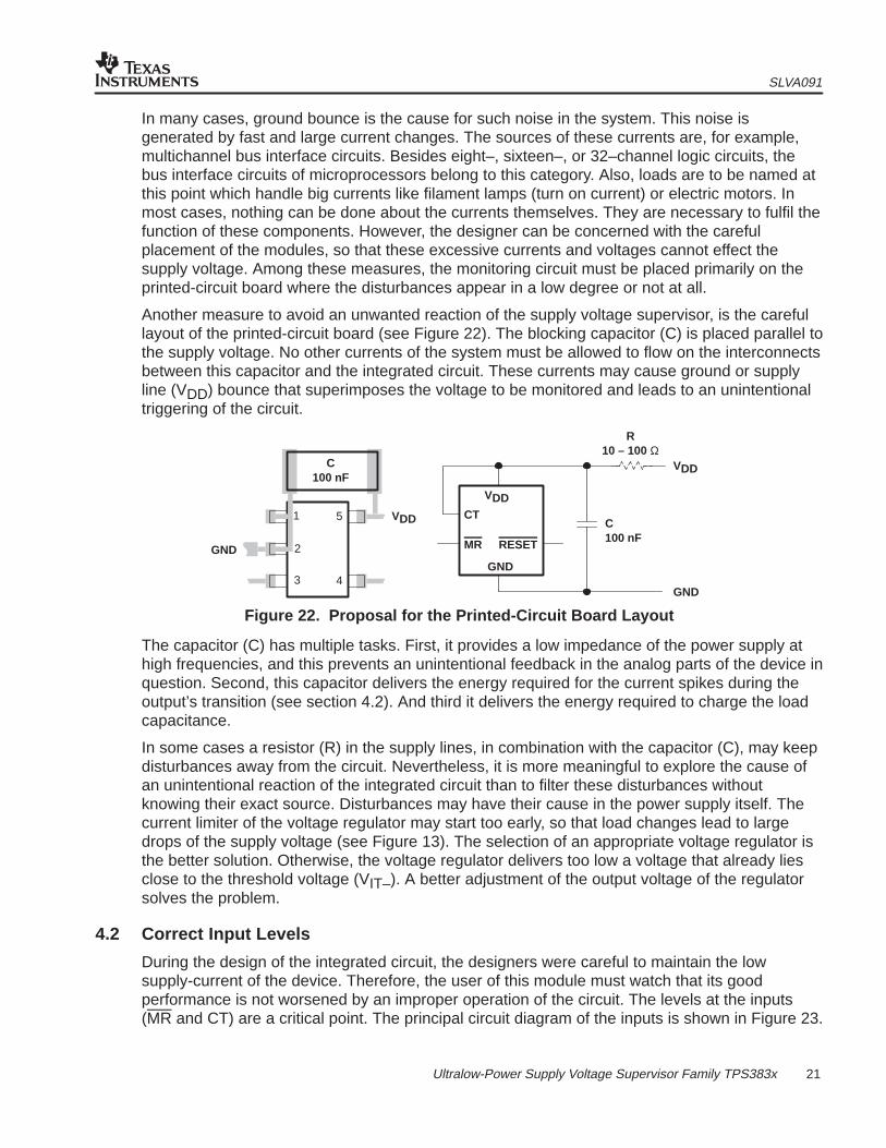
In many cases, ground bounce is the cause for such noise in the system. This noise isgenerated by fast and large current changes. The sources of these currents are, for example,multichannel bus interface circuits. Besides eight–, sixteen–, or 32–channel logic circuits, thebus interface circuits of microprocessors belong to this category. Also, loads are to be named atthis point which handle big currents like filament lamps (turn on current) or electric motors. Inmost cases, nothing can be done about the currents themselves. They are necessary to fulfil thefunction of these components. However, the designer can be concerned with the carefulplacement of the modules, so that these excessive currents and voltages cannot effect thesupply voltage. Among these measures, the monitoring circuit must be placed primarily on theprinted-circuit board where the disturbances appear in a low degree or not at all.
Another measure to avoid an unwanted reaction of the supply voltage supervisor, is the carefullayout of the printed-circuit board (see Figure 22). The blocking capacitor (C) is placed parallel tothe supply voltage. No other currents of the system must be allowed to flow on the interconnectsbetween this capacitor and the integrated circuit. These currents may cause ground or supplyline (VDD) bounce that superimposes the voltage to be monitored and leads to an unintentionaltriggering of the circuit.
3
2
4
51
GND
VDD
C100 nF
VDDCT
MR
GND
RESET
R10 – 100 Ω
C100 nF
VDD
GND
Figure 22. Proposal for the Printed-Circuit Board Layout
The capacitor (C) has multiple tasks. First, it provides a low impedance of the power supply athigh frequencies, and this prevents an unintentional feedback in the analog parts of the device inquestion. Second, this capacitor delivers the energy required for the current spikes during theoutput’s transition (see section 4.2). And third it delivers the energy required to charge the loadcapacitance.
In some cases a resistor (R) in the supply lines, in combination with the capacitor (C), may keepdisturbances away from the circuit. Nevertheless, it is more meaningful to explore the cause ofan unintentional reaction of the integrated circuit than to filter these disturbances withoutknowing their exact source. Disturbances may have their cause in the power supply itself. Thecurrent limiter of the voltage regulator may start too early, so that load changes lead to largedrops of the supply voltage (see Figure 13). The selection of an appropriate voltage regulator isthe better solution. Otherwise, the voltage regulator delivers too low a voltage that already liesclose to the threshold voltage (VIT–). A better adjustment of the output voltage of the regulatorsolves the problem.
4.2 Correct Input Levels
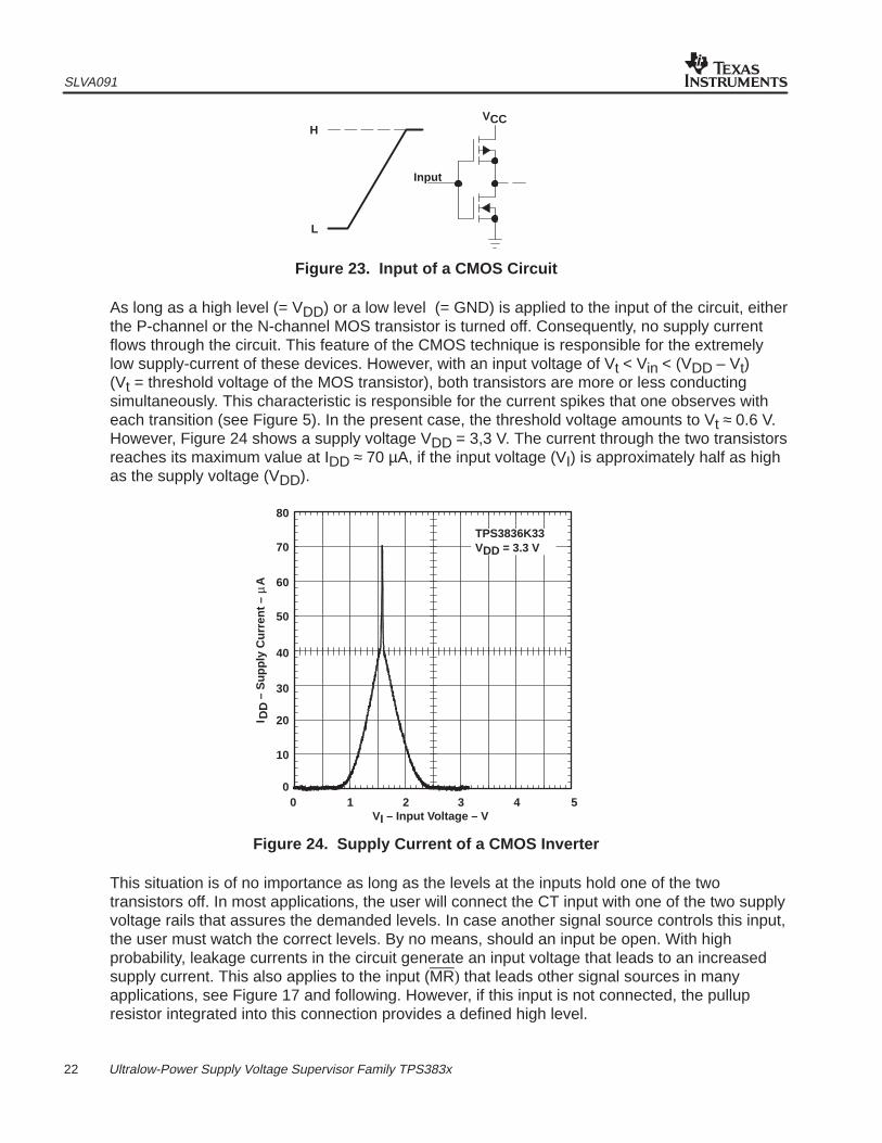
During the design of the integrated circuit, the designers were careful to maintain the lowsupply-current of the device. Therefore, the user of this module must watch that its goodperformance is not worsened by an improper operation of the circuit. The levels at the inputs(MR and CT) are a critical point. The principal circuit diagram of the inputs is shown in Figure 23.
SLVA091
22 Ultralow-Power Supply Voltage Supervisor Family TPS383x
H
L
Input
VCC
Figure 23. Input of a CMOS Circuit
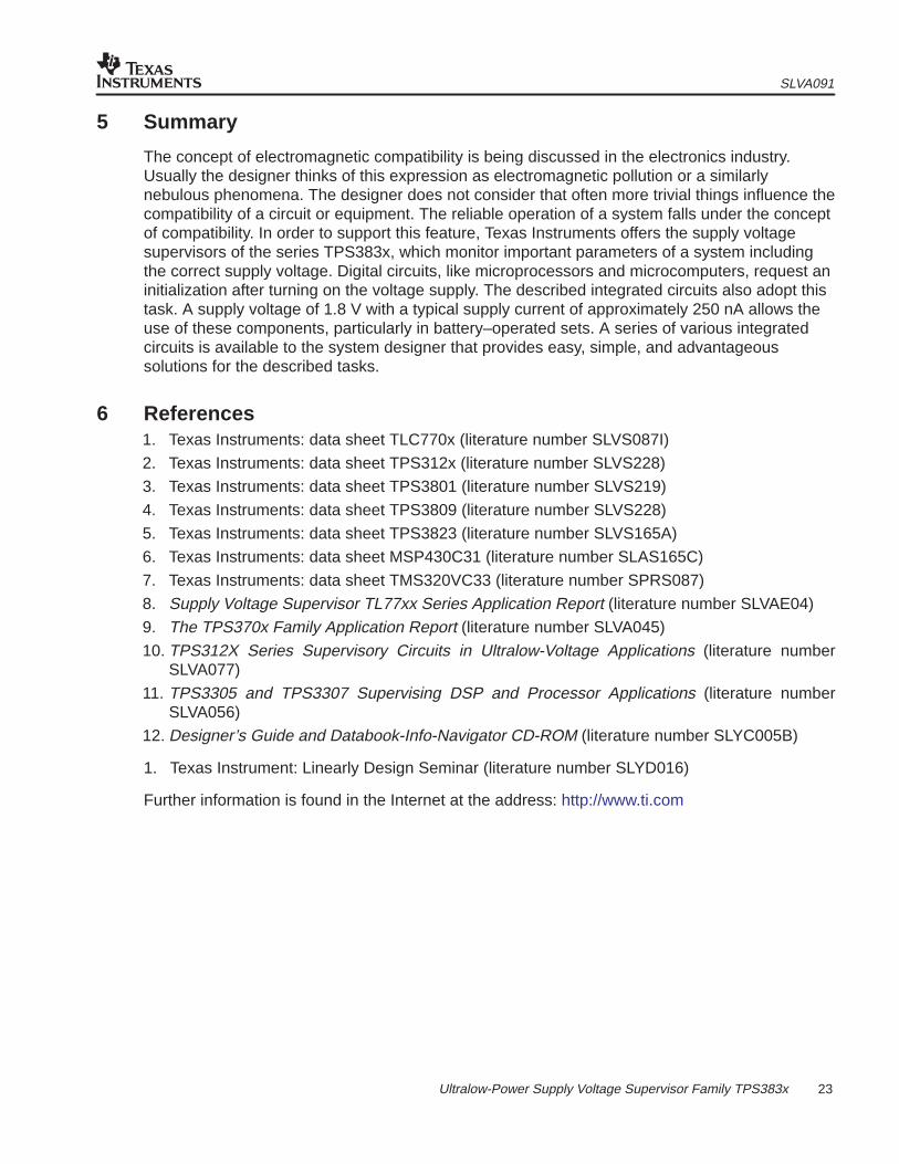
As long as a high level (= VDD) or a low level (= GND) is applied to the input of the circuit, eitherthe P-channel or the N-channel MOS transistor is turned off. Consequently, no supply currentflows through the circuit. This feature of the CMOS technique is responsible for the extremelylow supply-current of these devices. However, with an input voltage of Vt < Vin < (VDD – Vt) (Vt = threshold voltage of the MOS transistor), both transistors are more or less conductingsimultaneously. This characteristic is responsible for the current spikes that one observes witheach transition (see Figure 5). In the present case, the threshold voltage amounts to Vt ≈ 0.6 V.However, Figure 24 shows a supply voltage VDD = 3,3 V. The current through the two transistorsreaches its maximum value at IDD ≈ 70 µA, if the input voltage (VI) is approximately half as highas the supply voltage (VDD).
60
40
10
30
0 1 2 3 4 50
20
50
70
80
TPS3836K33VDD = 3.3 V
– S
uppl
y C
urre
nt –
I DD
Aµ
VI – Input Voltage – V
Figure 24. Supply Current of a CMOS Inverter
This situation is of no importance as long as the levels at the inputs hold one of the twotransistors off. In most applications, the user will connect the CT input with one of the two supplyvoltage rails that assures the demanded levels. In case another signal source controls this input,the user must watch the correct levels. By no means, should an input be open. With highprobability, leakage currents in the circuit generate an input voltage that leads to an increasedsupply current. This also applies to the input (MR) that leads other signal sources in manyapplications, see Figure 17 and following. However, if this input is not connected, the pullupresistor integrated into this connection provides a defined high level.
SLVA091
23 Ultralow-Power Supply Voltage Supervisor Family TPS383x
5 Summary
The concept of electromagnetic compatibility is being discussed in the electronics industry.Usually the designer thinks of this expression as electromagnetic pollution or a similarlynebulous phenomena. The designer does not consider that often more trivial things influence thecompatibility of a circuit or equipment. The reliable operation of a system falls under the conceptof compatibility. In order to support this feature, Texas Instruments offers the supply voltagesupervisors of the series TPS383x, which monitor important parameters of a system includingthe correct supply voltage. Digital circuits, like microprocessors and microcomputers, request aninitialization after turning on the voltage supply. The described integrated circuits also adopt thistask. A supply voltage of 1.8 V with a typical supply current of approximately 250 nA allows theuse of these components, particularly in battery–operated sets. A series of various integratedcircuits is available to the system designer that provides easy, simple, and advantageoussolutions for the described tasks.
6 References1. Texas Instruments: data sheet TLC770x (literature number SLVS087I)
2. Texas Instruments: data sheet TPS312x (literature number SLVS228)
3. Texas Instruments: data sheet TPS3801 (literature number SLVS219)
4. Texas Instruments: data sheet TPS3809 (literature number SLVS228)
5. Texas Instruments: data sheet TPS3823 (literature number SLVS165A)
6. Texas Instruments: data sheet MSP430C31 (literature number SLAS165C)
7. Texas Instruments: data sheet TMS320VC33 (literature number SPRS087)
8. Supply Voltage Supervisor TL77xx Series Application Report (literature number SLVAE04)
9. The TPS370x Family Application Report (literature number SLVA045)
10. TPS312X Series Supervisory Circuits in Ultralow-Voltage Applications (literature numberSLVA077)
11. TPS3305 and TPS3307 Supervising DSP and Processor Applications (literature numberSLVA056)
12. Designer’s Guide and Databook-Info-Navigator CD-ROM (literature number SLYC005B)
1. Texas Instrument: Linearly Design Seminar (literature number SLYD016)
Further information is found in the Internet at the address: http://www.ti.com
IMPORTANT NOTICE
Texas Instruments and its subsidiaries (TI) reserve the right to make changes to their products or to discontinueany product or service without notice, and advise customers to obtain the latest version of relevant informationto verify, before placing orders, that information being relied on is current and complete. All products are soldsubject to the terms and conditions of sale supplied at the time of order acknowledgment, including thosepertaining to warranty, patent infringement, and limitation of liability.
TI warrants performance of its semiconductor products to the specifications applicable at the time of sale inaccordance with TI’s standard warranty. Testing and other quality control techniques are utilized to the extentTI deems necessary to support this warranty. Specific testing of all parameters of each device is not necessarilyperformed, except those mandated by government requirements.
Customers are responsible for their applications using TI components.
In order to minimize risks associated with the customer’s applications, adequate design and operatingsafeguards must be provided by the customer to minimize inherent or procedural hazards.
TI assumes no liability for applications assistance or customer product design. TI does not warrant or representthat any license, either express or implied, is granted under any patent right, copyright, mask work right, or otherintellectual property right of TI covering or relating to any combination, machine, or process in which suchsemiconductor products or services might be or are used. TI’s publication of information regarding any thirdparty’s products or services does not constitute TI’s approval, warranty or endorsement thereof.
Copyright 2000, Texas Instruments Incorporated