Embed Size (px)
Citation preview
1
ULTRAFAST OPTICAL SPECTROSCOPIC STUDY OF SEMICONDUCTORS IN HIGH MAGNETIC FIELDS
By
XIAOMING WANG
A DISSERTATION PRESENTED TO THE GRADUATE SCHOOL OF THE UNIVERSITY OF FLORIDA IN PARTIAL FULFILLMENT
OF THE REQUIREMENTS FOR THE DEGREE OF DOCTOR OF PHILOSOPHY
UNIVERSITY OF FLORIDA
2008

2
© 2008 Xiaoming Wang

3
To my wife and my daughter

4
ACKNOWLEDGMENTS
First of all, I would like to express my deep gratitude to my advisor, Professor David
Reitze, for his supervision, instruction, encouragement, tremendous support and friendship
during my Ph.D. He guided me into a beautiful world of ultrafast optics. His profound
knowledge of ultrafast optics, condensed matter physics and his teaching style always impress
me and will help me all through my life.
I wish to thank my supervisory committee, Prof. Stanton, Prof. Tanner, Prof. Rinzler and
Prof. Kleiman, for their instructions for my thesis and finding errors in my thesis manuscript.
I would like to give my sincere thanks to the visible optics staff scientists at the National
High Magnetic Field Laboratory, Dr. Xing Wei and Dr. Stephen McGill, for their excellent
technical support for our experiments. I learned plenty of knowledge about spectrometers, fibers,
cryogenics, magnets and LabView program from them. Also I give my special thanks to Dr.
Brandt, former director of DC facility at NHMFL, for his great administrative assistance.
I appreciate the experimental and theoretical supervisions we received for our research
projects from Prof. Stanton from University of Florida, Prof. Kono from Rice University and
Prof. Belyanin from Texas A&M University. Special thanks should be given to my research
collaborators, Dr. Young-dahl Cho and Jinho Lee. Our research projects would not be so
successful without their contribution.
This work is supported by National Science Foundation and In House Research Program at
the National High Magnetic Field Laboratory.
Finally I want to send my warmest thanks to my wife and my daughter, my parents and
parents in law for their endless love and support. I could not complete my studies without their
emotional and financial support.
5
TABLE OF CONTENTS page
ACKNOWLEDGMENTS ...............................................................................................................4
LIST OF TABLES...........................................................................................................................8
LIST OF FIGURES .........................................................................................................................9
ABSTRACT...................................................................................................................................14
CHAPTER
1 INTRODUCTION AND OVERVIEW ..................................................................................16
1.1 Semiconductors and Quantum Wells ............................................................................17 1.2 Magneto-spectroscopy in High Magnetic Fields ..........................................................18 1.3 Motivation for Performing Ultrafast Spectroscopy in High Magnetic Fields ..............19
1.3.1 Quantum Optical Processes in Semiconductors--Superfluorescence ................19 1.3.2 Studies of Technologically Interesting Materials ..............................................20
2 HIGH FIELD MAGNETO-OPTICAL TECHNIQUES AND FUNDAMENTALS OF MAGNETO-OPTICAL SPECTROSCOPY...........................................................................24
2.1 Introduction...................................................................................................................24 2.2 Basic Background of Optical Response of Solids.........................................................24 2.3 Magneto-spectroscopy of Semiconductors--Methods...................................................27
2.3.1 Transmission Spectroscopy ...............................................................................27 2.3.2 Reflection Spectroscopy ....................................................................................28 2.3.3 Photoluminescence (PL) Spectroscopy..............................................................29
2.4 Time-resolved Spectroscopy of Semiconductors..........................................................29 2.5 CW Optical Experimental Capabilities at the NHMFL ................................................32 2.6 Development of Ultrafast Magneto-optical Spectroscopy at NHMFL.........................34
2.6.1 Introduction of Ultrafast Optics .........................................................................34 2.6.2 Magnet and Cryogenics for Ultrafast Optics at NHMFL ..................................35 2.6.3 Ultrafast Light Sources ......................................................................................36
2.6.3.1 Ti:Sapphire femtosecond oscillator..........................................................36 2.6.3.2 Chirped pulse amplifier ............................................................................37 2.6.3.3 Optical parametric amplifier ....................................................................38 2.6.3.4 Streak camera ...........................................................................................39
3 ELECTRONIC STATES OF SEMICONDUCTOR QUANTUM WELL IN MAGNETIC FIELD...............................................................................................................57
3.1 Introduction...................................................................................................................57 3.2 Band Structure of Wurzite and Zinc Blend Structure Bulk Semiconductors................57 3.3 Selection Rules..............................................................................................................60

6
3.4 Quantum Well Confinement .........................................................................................61 3.5 Density of States in Bulk Semiconductor and Semiconductor Nanostructures ............63 3.6 Magnetic Field Effect on 2D Electron Hole Gas in Semiconductor Quantum Well ....64 3.7 Excitons and Excitons in Magnetic Field......................................................................66
3.7.1 Excitons..............................................................................................................66 3.7.2 Magneto –excitons .............................................................................................67
4 MAGNETO-PHOTOLUMINESCENCE IN INGAAS QWS IN HIGH MAGNETIC FIELDS...................................................................................................................................78
4.1 Background ...................................................................................................................78 4.2 Motivation for Investigating PL from InGaAs MQW in High Magnetic Fields
Using High Power Laser Excitation..............................................................................81 4.3 Sample Structure and Experimental Setup....................................................................82 4.4 Experimental Results and Discussion ...........................................................................82
4.4.1 Prior Study of InxGa1-xAs/GaAs QW Absorption Spectrum .............................82 4.4.2 PL Spectrum Excited with High Peak Power Ultrafast Laser in High
Magnetic Field ..................................................................................................84 4.5 Summary .......................................................................................................................87
5 INVESTIGATIONS OF COOPERATIVE EMISSION FROM HIGH-DENSITY ELECTRON-HOLE PLASMA IN HIGH MAGNETIC FIELDS .........................................98
5.1 Introduction to Superfluorescence (SF) ........................................................................98 5.1.2 Spontaneous Emission and Amplified Spontaneous Emission..........................99 5.1.3 Coherent Emission Process--Superradiance or Superfluorescence .................101 5.1.4 Theory of Coherent Emission Process--SR or SF in Dielectric Medium ........106
5.2 Cooperative Recombination Processes in Semiconductor QWs in High Magnetic Fields ...........................................................................................................................109 5.2.1 Characteristics of SF Emitted from InGaAs QW in High Magnetic Field. .....110 5.2.2 Single Shot Random Directionality of PL Emission .......................................112 5.2.3 Time Delay between the Excitation Pulse and Emission.................................113 5.2.4 Linewidth Effect with the Carrier Density.......................................................113 5.2.5 Emission intensity Effect with Carrier Density ...............................................113 5.2.6 Threshold Behavior..........................................................................................114 5.2.7 Exponential Growth of Emission Strength with the Excited Area ..................114
5.3 Experiments and Setup................................................................................................115 5.4 Experimental Results and Discussion .........................................................................117
5.4.1 Magnetic Field and Power Dependence of PL ................................................117 5.4.2 Single Shot Experiment for Random Directionality of In Plane PL................119 5.4.3 Control of Cherence of In Plane PL from InGaAs QW in High Magnetic
Field ................................................................................................................120 5.4.4 Discussion........................................................................................................121
5.5 Summary .....................................................................................................................125
6 STUDY OF CARRIER DYNAMICS OF ZINC OXIDE SEMICONDUCTORS WITH TIME RESOLVED PUMP-PROBE SPECTROSCOPY .....................................................140

7
6.1 Introduction.................................................................................................................140 6.2 Background of Crystal Structure and Band Structure of ZnO Semiconductors .........141 6.3 Valence Band Symmetry and Selection Rules of Excitonic Optical Transition in
ZnO Semiconductors...................................................................................................142 6.4 Impurity Bound Exciton Complex (I line) in ZnO and Zeeman Splitting ..................144 6.5 Samples and Experimental Setup for Reflection and PL Measurement .....................146 6.6 Results and Discussion................................................................................................147 6.7 Time Resolved Studies of Carrier Dynamics in Bulk ZnO, ZnO Epilayers, and
ZnO Nanorod ..............................................................................................................149 6.8 Experimental Results and Discussion .........................................................................151
6.8.1 Relaxation Dynamics of A-X and B-X in Bulk ZnO.......................................151 6.8.2 Relaxation Dynamics of A-X and B-X in ZnO Epilayer and Nanorod ...........152
7 CONCLUSION AND FUTURE WORK .............................................................................172
APPENDIX
A SAMPLE MOUNT AND PHOTOLUMINESCENCE COLLECTION..............................176
B PIDGEON-BROWN MODEL .............................................................................................179
LIST OF REFERENCES.............................................................................................................182
BIOGRAPHICAL SKETCH .......................................................................................................190

8
LIST OF TABLES
Table page 1-1 Some band parameters for some III-V compound semiconductors and their alloys. ........22
3-1 Periodic parts of Bloch functions in semiconductors ........................................................70
3-2 Selection rules for interband transitions using the absolute values of the transition matrix elements..................................................................................................................71
5-1 Some experimental conditions for observation of super fluorescence in HF gas............126
6-1 Some parameters of ZnO bulk semiconductors ...............................................................155

9
LIST OF FIGURES
Figure page
1-1 Physical and energy structure of semiconductor multiple quantum well ..........................23
2-1 Transmission spectrum of InGaAs/GaAs MQW at 30 T and 4.2 K ..................................40
2-2 Reflection spectrum of ZnO epilayer at 4.2K....................................................................41
2-3 e-h recombination process and photoluminescence spectrum in semicondcutros.............42
2-4 Simple illustration of optical pump-probe transient absorption or reflection experiment..........................................................................................................................43
2-5 Experimental setup for optical pump-probe spectroscopy and TRDR spectrum of ZnO ....................................................................................................................................44
2-6 Time resolved photoluminescence spectrum of InxGa1-xAs/AlGaAs MQW at 4.2K ............
2-7 Technical drawing of the 30 Tesla resistive magnet in cell 5 at NHMFL.........................46
2-8 Technical drawing of cryostat and optical probe for CW optical spectroscopy at NHMFL..............................................................................................................................47
2-9 Block diagram of the CW magneto optical experiment setup at the NHMFL. .................48
2-10 Schematic diagram of modified magneto optical cryostat for direct ultrafast optics. .......49
2-11 Technical drawing of the 17 Tesla superconducting magnet SCM3 in cell 3 at NHMFL..............................................................................................................................50
2-12 Technical drawing of the special optical probe designed for superconducting magnet 3 in cell 3 at the NHMFL...................................................................................................51
2-13 Schematic diagram of Coherent Mira 900F femtosecond laser oscillator.........................52
2-14 Schematic diagram of Coherent Legend–F chirped pulse amplifier (CPA) ......................53
2-15 Top view scheme of layout of the optical elements and beam path in TOPAS OPA........54
2-16 Operation principle of a streak camera ..............................................................................55
2-17 Block diagram of ultrafast optics experimental setup in cell 3 and 5 at NHMFL.............56
3-1 Band structure of Zinc blend semiconductors ...................................................................72
3-2 Band structure of wurzite structure semiconductors..........................................................73

10
3-3 Schematic diagrams of band alignment and confinement subbands in type I semiconductor quantum well. ............................................................................................74
3-4 Density of states in different dimensions...........................................................................75
3-5 Electronic energy states in a semiconductor quantum well in the presence of a magnetic field.....................................................................................................................76
3-6 Calculation of free electron hole pair energy and magneto exciton energy of InxGa1-
xAs/GaAs QW as function of magnetic field.....................................................................77
4-1 Magneto abosorption spectrum and schematic diagram of interband Landau level transitions...........................................................................................................................88
4-2 Magnetophotoluminescence experimental results of band gap change and effective mass change. ......................................................................................................................89
4-3 Valence band mixing of heavy hole and light hole subbands in semiconductor quantum well......................................................................................................................90
4-4 Structure of In0.2Ga0.8As/GaAs multiple quantum well .....................................................91
4-5 Faraday configuration in magnetic field ............................................................................92
4-6 Energy levels of electron and hole quantum confinement states in InxGa1-xAs quantum wells ....................................................................................................................93
4-7 Magneto-photoluminescence spectrum of InxGa1-xAs quantum well at 10K ....................94
4-8 Landau fan diagram of absorption and PL spectrum of InxGa1-xAs quantum well in magnetic field up to 30 T. ..................................................................................................95
4-9 Magneto-PL and excitation density dependence of the integrated PL in InxGa1-xAs quantum wells at 20 T and 10 K ........................................................................................96
4-10 Theoretical calculation and experimental results of PL in high magnetic field ................97
5-1 Spontaneous emission and amplified spontaneous emission process of a two level atom system .....................................................................................................................128
5-2 Four steps in the formation of collective spontaneous emission--SF in N atom system .129
5-3 Schematic diagram of the configuration for collection of in plane PL from InGaAs multiple QW in high magnetic field ................................................................................130
5-4 Experimental schematic showing the configuration for a single shot experiment on InxGa1-xAs QWs...............................................................................................................131
11
5-6 Fitting method to determine line widths using a Lorentzian and Gaussian function for the sharp peak and broader lower-energy peak................................................................133
5-7 Excitation power dependent PL spectrum and fitting results of in plane emission .........134
5-8 Excitation spot size effect on the in plane PL emission...................................................135
5-9 Single shot directionality measurement of in plane PL emission in SF regime ..............136
5-10 Single shot directionality measurement of in plane PL emission in ASE regime ...........137
5-11 Schematic diagram of the configuration of control of emission directionality in InxGa1-xAs multiple QW ..................................................................................................138
5-12 Control of coherence of in plane PL emission in InxGa1-xAs QW...................................139
6-1 Top view of the lattice structure of a wurtzite ZnO crystal .............................................156
6-2 The orientation of light polarization with respect to the ZnO unit cell ...........................157
6-3 Band structures and symmetry of each band of a ZnO semiconductor. ..........................158
6-4 Schematic of types of impurity bound exciton complexes ..............................................159
6-5 Energy diagram of Zeeman splitting of neutral bound excitons in ZnO .........................160
6-6 Schematic diagram of Voigt configuration of c-plane ZnO in magnetic field ................161
6-7 Reflection spectrum of a-plane bulk ZnO semiconductor for different linear optical polarization at 4.2K..........................................................................................................162
6-8 The magneto-PL spectrum of a and c-plane bulk ZnO sample and Zeeman splitting at 4.2K..............................................................................................................................163
6-9 Comparison of reflection and PL spectrum of c-plane bulk ZnO....................................164
6-10 Comparison of reflection and PL spectrum of c-plane epilayer ZnO at 4.2 K ................165
6-11 Schematic diagram of the pump-probe experimental setup for measuring TRDR of ZnO semiconductors. .......................................................................................................166
6-12 TRDR plots of a-plane bulk ZnO semiconductor at 4.2K and exponential decay fitting line.........................................................................................................................167
6-13 Fast decay in TRDR of A-X in a-plane bulk ZnO and the fitting with convolution of Gaussian function and exponential decay function .........................................................168
6-14 Temperature dependent TRDR of A-X recombination in c-plane bulk ZnO ..................169
12
6-15 TRDR plots of excitonic recombination in ZnO epilayer for different exciton states.....170
6-16 Experimental TRDR plot of ZnO nanorod sample at 10K and fitting result...................171
A-1 Detailed schematic diagram of sample mount and PL collection used in the experiment........................................................................................................................178
13
LIST OF ABBREVIATIONS
BEC Bound exciton complex
CCD Charged coupled device
CPA Chirped pulse amplifier
CW Continuous wave
DOS Density of states
LL Landau level
MQW Multiple quantum well
NHMFL National High Magnetic Field Laboratory
OPA Optical parametric amplifier
PL Photoluminescence
PMT Photomultiplier tube
SCM Superconducting magnet
SF Superfluorescence
TRDR Time resolved differential reflectivity
X Exciton

14
Abstract of Dissertation Presented to the Graduate School of the University of Florida in Partial Fulfillment of the Requirements for the Degree of Doctor of Philosophy
ULTRAFAST OPTICAL SPECTROSCOPIC STUDY OF SEMICONDUCTORS IN HIGH MAGNETIC FIELDS
By
Xiaoming Wang
May 2008
Chair: David H. Reitze Major: Physics
We studied the magneto-excitonic states of two-dimensional (2D) electron and hole gas in
InxGa1-xAs/GaAs multiple quantum wells (MQW) with continuous wave (CW) optical
spectroscopic methods, including transmission and photoluminescence spectroscopy, in high
magnetic field up to 30 Tesla. Interband Landau level (LL) transitions are clearly identified. The
anticrossing behavior in the Landau fan diagram of the transmission spectrum is interpreted as
dark and bright exciton mixing due to Coulomb interaction. With the unique facility of ultrafast
optics at National High Magnetic Field Laboratory, we are able to change the 2D electron hole
gas into 0D and increase density of each quantum state as well as the actual sheet carrier density
in the quantum well (up to 1012cm-2) dramatically. Under these conditions, interactions between
electron and hole pairs confined in 0D system play a very important role in the electron hole
recombination process. With high power pulsed lasers and cryogenic equipment, we studied the
strong magneto photoluminescence emission from InxGa1-xAs/GaAs MQW in high magnetic
field. By analyzing the power dependent, field dependent and direction dependent PL spectrum,
the abnormally strong PL emission from InxGa1-xAs/GaAs MQW in high magnetic field is found
to be the result of cooperative recombination of high density magneto electron-hole plasmas.

15
This abnormally strong photoluminescence from InxGa1-xAs/GaAs MQW in high magnetic field
under CPA excitation is proved to be superfluorescence.
We studied CW spectroscopic properties of ZnO semiconductors including reflectivity and
photoluminescence at different crystal orientations. A, B excitonic states in ZnO semiconductors
are clearly identified. Also, with time resolved pump probe spectroscopy, we studied the carrier
dynamics of excitonic states of A and B in bulk ZnO as well as ZnO epilayer and nanorods.

16
CHAPTER 1 INTRODUCTION AND OVERVIEW
During the past few decades, the transport and optical properties of electron (e) hole (h)
gas in two-dimensional (2D) semiconductor quantum well (QW) in magnetic field have been
studied extensively in theory and experiments [1-5]. However most of the magneto-optical
studies are based on continuous wave (CW) optics or low magnetic field.
In this dissertation, we first investigate the magneto-excitonic states of 2D electron and
hole gas in InxGa1-xAs/GaAs multiple quantum wells (MQW) with CW optical spectroscopic
methods, including transmission and photoluminescence (PL) spectroscopy. With the unique
facility that exists at National High Magnetic Field Laboratory (30 Tesla magnetic field
combined with intense ultrashort pulse lasers), we are able to change the 2D electron hole gas
into a quasi-0D system, and increase carrier density of states of each quantum state as well as
actual sheet carrier density dramatically. Under these conditions, the excitonic effect is
suppressed because the Coulomb interaction between high-density e-h pairs is screened, while
the interactions between e-h pairs confined in this quasi 0D system play a very important role in
the recombination process.
With high power pulsed lasers and cryogenic equipment, we studied the strong magneto-
PL emission from InxGa1-xAs/GaAs MQW in high magnetic fields. With analyzing the power
dependent, field dependent and single shot direction dependent PL spectrum, the abnormally
strong PL emission is found to be result from a cooperative recombination process of high
density magneto e-h plasmas, which is called superfluorescence (SF).
The second part of this thesis focuses on the CW and ultrafast optical spectroscopic study
of ZnO semiconductors. Due to its unique band gap (~3.35 eV) and large exciton binding energy
(~60mev) at room temperature [6-10], these are promising materials for optoelectronic

17
applications, such as blue and ultraviolet emitters and detectors. By analyzing the CW spectra,
the band structures, excitonic and impurity bound excitonic states are identified. By using pump-
probe spectroscopy, the dynamics of different excitonic states are studied in bulk ZnO, ZnO
epilayer and nanorods.
1.1 Semiconductors and Quantum Wells
By using epitaxial growth such as molecular beam epitaxy (MBE) and metal organic
chemical vapor deposition (MOCVD), modern science and technology have provided us the
methods of manufacturing a very thin epitaxial layer (~nm) of a semiconductor compound on
another different semiconductor with interface of very high precision (atomic precision), thus
allowing for ‘quantum-engineered’ materials and structures.
The optical properties of semiconductor QWs have been extensively studied [11-15], and
many physical phenomena have been investigated thoroughly, i.e. interband transitions, inter-
subband transitions.
Figure1-1 shows physical and band structure of III-V or II-VI group semiconductor
multiple quantum wells, composed of periods of ABAB…, A and B are two layers of different
type of semiconductor compounds, i.e. InXGa1-xAs and GaAs. The bandgap of compound B (the
well) lies within the bandgap of the compound A (the barrier). The thickness of barrier A is
typically greater than 10 nm, so that carriers will be confined in the QW layers. This particularly
unique property of semiconductor heterojunctions provides us an ideal system for studying the
interesting physics and application of device in two dimensional electron gas system--carriers in
QWs are confined in the z direction, the growth direction of QW, and still move freely in the
quantum well plane, or x-y direction. The interface between barrier and well imposes
confinement on carriers in QWs, which results in the formation of discrete quantum states in
both conduction and valence band. In a semiconductor, if an electron in valence band is excited

18
to conduction band as a free electron, a hole will be left in valence band. Through the Coulomb
interaction, this electron hole pair can form a hydrogen atom (H) like quasi-atom system: an
exciton (X). In a semiconductor QWs, due to the spatial confinement and discrete quantum state
confinement, excitonic effects are more pronounced than semiconductor bulks [16-20]. These
discrete excitonic states of exciton provide a unique system to study quantum optical processes
of carriers in semiconductor quantum wells.
1.2 Magneto-Spectroscopy in High Magnetic Fields
In the presence of a high magnetic field, the cyclotron energy cωh of a charge carrier is
greater than the exciton binding energy Eb (for GaAs, cωh =4Eb above 20T). Thus, we open a
new regime to study semiconductor magneto-optics, where the magnetic field effect due to the
formation of Landau levels (LLs) will suppress the exciton effect. Also, in high magnetic field,
electrons and holes populate on LLs, which provide us a system to study the mid infrared light
driven intraband LL transitions. Many new physical processes can be explored in semiconductor
quantum wells at high magnetic fields [21-25].
Another impact that applied high magnetic fields have on a semiconductor QW is an
alteration of the carrier confinement. Free carriers are confined in QW plane since the magnetic
length lB is on the order of a few nm. At high magnetic fields, the density of states (DOS) of a
two dimensional electron gas system will evolve into a zero dimensional system, like a quantum
dot; the separation between LLs varies with the intensity of magnetic field. Magneto-excitons (or
magneto-plasmas) confined in quasi-nanorods in semiconductor QWs at high magnetic field
provides us with an atomic-like system with tunable internal energy levels to study quantum
optics in solids.
19
In early studies of magneto-optics in semiconductor quantum wells, light sources used in
the experiments were usually continuous wave (CW) white light or CW lasers (see Chapter.2.5
for detail), which provided static spectroscopic information only. In the past twenty years, with
the development of ultrafast laser technology and magnet technology, time resolved
spectroscopic studies of magneto optical experiments like time resolved Kerr rotation or time
resolved Faraday rotation can be carried out in a split coil superconducting magnet [26-30].
However, time resolved dynamics of magneto-excitons populate on LLs in semiconductor QW
has been carried out at fields less than 12 T [31-33] and not yet been realized at higher magnetic
fields. Furthermore, in high magnetic fields, sheet carrier density in QW can also increased
dramatically due to the 0D like DOS at each LL. If the excitation power of the pulsed laser is
very large, i.e., as that achievable with amplified ultafast laser systems (CPA) as the excitation
light source, we can create a carrier density in excess of 1013/cm-2 in the QWs. In this case, the e-
h response in the QW will be dominated by plasma-like instead of exciton-like behavior. These
high-density magneto-plasmas confined in QWs interact with each other and correlate to each
other before they start to recombine. This leads to many new and exciting physical phenomena,
as we discussed later.
1.3 Motivation for Performing Ultrafast Spectroscopy in High Magnetic Fields
1.3.1 Quantum Optical Processes in Semiconductors--Superfluorescence
In high magnetic field, e-h pairs are confined in a quasi 0D structure. Therefore, we can
use this atom like system to study quantum optics in electron hole pair in high magnetic field, i.e.
strong electromagnetic field induced energy splitting--AC Stark Effect [34] and cooperative
recombination process--Superfluorescence [35].
In an atomic ensemble, if the atoms are in excited state, they will relax down to ground
state through emission of photons. This process is called spontaneous emission if there is no

20
interaction between atoms during the emission. In the case where the decoherence time of the
atom is significantly greater than the spontaneous emission time, due to the interaction between
atoms, the atomic ensemble can evolve into to a coherent state and emit a burst of photons
through a cooperative radiative process called superfluorescence. This type of emission,
characterized by its short pulse width and high intensity compared to spontaneous emission, has
been observed in rarefied gas systems [36], however, due to very short carrier decoherent time in
solid, superflorencence has not been observed so far.
1.3.2 Studies of Technologically Interesting Materials
In order to study quantum optics in semiconductor QW in high magnetic field, the intrinsic
properties of semiconductor material are very crucial to observe quantum processes. These
properties include band structure, electron and hole effective masses, QW structure, and barrier
and well compositions.
Among all the III-V group and II-VI group semiconductor materials, III-V group
compounds such as InxGa1-xAs/GaAs, InxGa1-xAs /InP, InxGa1-xAs /AlGaAs and GaAs/AlGaAs
QW series are the best materials to study quantum optical phenomena of e-h pairs in
semiconductor QWs.
These materials have been thoroughly studied using magneto-optical spectroscopy and
their band structures are well known [37, 38]. First, their band gaps energy are in the near
infrared region, which is very suitable for excitation with Ti: Sapphire ultrafast lasers; second,
the electron subband and valence hole subband are separated reasonably well which cause less
band complexity; third, the electron and hole effective mass in these materials are relatively
small and the exciton binding energy are relatively large (~10 meV), which make it easy to
observed higher LLs in high magnetic field. Some band structure constants of some III-V group
semiconductors are listed in Table 1-1.

21
In this dissertation, we selected InxGa1-xAs/GaAs MQW for the host material for 2D e-h
gas. The behaviors of high density e-h pairs under high power excitation in high magnetic field
are the main result in this dissertation.

22
Table 1-1. Some band parameters for some III-V compound semiconductors and their alloys. Parameters GaAs InAs InP ac(Å) 5.651 6.051 5.871
EΓg(mev) 15191 4171 14231
Exg (mev) 19811 14431 14801
Δso(mev) 3411 3901 1081
m*e(Г) 0.0671 0.0261 0.07951
m*e(X) 1.91 0.641 0.0771
m*hh(me) 0.451 0.411 0.641
m*lh(me) 0.0821 0.0261
1 Reference [37] ac is the crystal lattice constant in c direction. EΓ
g and Exg are the bandgaps at Γ and X point.
Δso is the spin orbit interaction, m*e(Г) and m*e(X) are the electron effective mass at Γ and x point. m*hh and m*lh are the effective mass of heavy hole and light hole.

23
(a)
(b) Figure 1-1. Physical and energy structure of semiconductor multiple quantum well.(a) Physical
structure type I semiconductor multiple quantum well, (b) Energy structure of type I semiconductor multiple quantum well
24
CHAPTER 2 HIGH FIELD MAGNETO-OPTICAL TECHNIQUES AND FUNDAMENTALS OF
MAGNETO-OPTICAL SPECTROSCOPY
2.1 Introduction
In this chapter, we introduce the basics on optical response theory, including
optical complex dielectric constant ε and refractive index n. We then give a background
in the techniques used to study optical properties of semiconductors, discussed the
experimental techniques of CW measurements on semiconductors, including
transmission, reflection and photoluminescence spectroscopy.
To understand the carrier dynamics in semiconductors, pump-probe spectroscopy is
employed. By understanding the how the dielectric constant ε and refractive index n
change with carrier density N, we can study the time resolved differential transmission
and reflection spectroscopy.
In addition, a detailed description is provided for the existing CW spectroscopic
experimental setup at the NHMFL that will be used for our measurements. Finally and
most importantly, to extend our research regime in high magnetic fields and ultrafast
lasers, we have developed an ultrafast facility at the NHMFL to study the ultrafast
magneto optical phenomena in high magnetic field. In this chapter, we give and overview
of the ultrafast facility and describe the technical details.
2.2 Basic Background of Optical Response of Solids
In a solid state system, including semiconductors, the optical response such as light
transmission and reflection is determined by the complex dielectric constant ε. Coupled
with an underlying model for the physics that relates to the dielectric function, the
knowledge of the dielectric function over a given spectral range completely specifies the
optical behavior of the material. In Drude’s model [39], ε is given by [40]
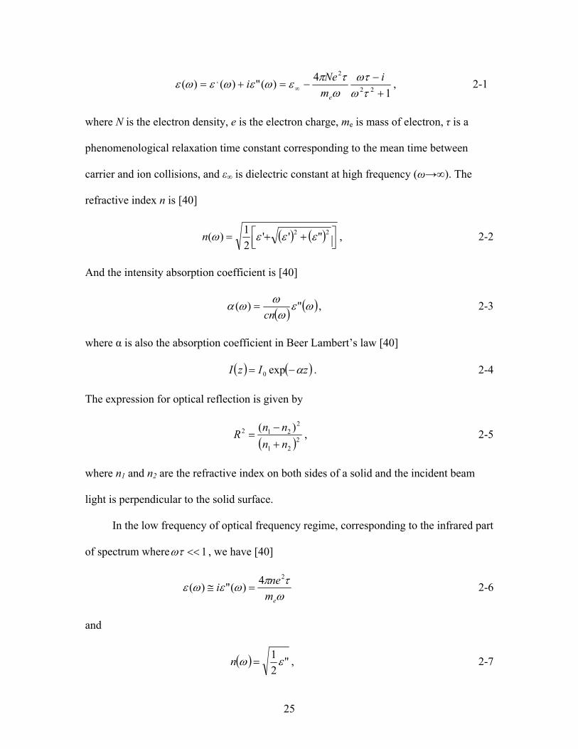
25
14)(")()( 22
2,
+−
−=+= ∞ τωωτ
ωτπεωεωεωε i
mNei
e
, 2-1
where N is the electron density, e is the electron charge, me is mass of electron, τ is a
phenomenological relaxation time constant corresponding to the mean time between
carrier and ion collisions, and ε∞ is dielectric constant at high frequency (ω→∞). The
refractive index n is [40]
( ) ( ) ⎥⎦⎤
⎢⎣⎡ ++= 22 "''
21)( εεεωn , 2-2
And the intensity absorption coefficient is [40]
( ) ( )ωεωωωα ")(
cn= , 2-3
where α is also the absorption coefficient in Beer Lambert’s law [40]
( ) ( )zIzI α−= exp0 . 2-4
The expression for optical reflection is given by
( )221
2212 )(
nnnnR
+−
= , 2-5
where n1 and n2 are the refractive index on both sides of a solid and the incident beam
light is perpendicular to the solid surface.
In the low frequency of optical frequency regime, corresponding to the infrared part
of spectrum where 1<<ωτ , we have [40]
ωτπωεωε
emnei
24)(")( =≅ 2-6
and
( ) "21 εω =n , 2-7
26
for the index of refraction and
( ) "2εωωαc
= 2-8
for the absorption coefficient.
In high optical frequency regime where 1>>ωτ , corresponding to ultraviolet part of
spectrum, we have [40]
( ) ( )⎟⎟
⎠
⎞
⎜⎜
⎝
⎛−=≅ ∞ 2
2
1'ω
ωεωεωε p , 2-9
where e
p mNe
∞
=επω
22 4 is plasma frequency.
For pωω > , we have [40]
( ) 'εω =n . 2-10
The relation between dielectric constant ε and optical susceptibility χ is [40]
( ) ( )ωπχωε 41+= , 2-11
χ is a complex parameter, given as
( ) ( ) ( )ωχωχωχ "' i+= . 2-12
Since the dielectric function ε and optical susceptibility χ have both real and
imaginary components, both of them will contribute the optical response such as the
transmission T and reflection R. Therefore, the optical resonant frequencies
correspondent to ε(ω) are not necessarily directly related to absorption peaks or dips on
the transmission and reflection spectrum. However, Kramers-Kronig transformations [40]
allow us to determine the real part of optical response function from the imaginary part at

27
all frequency and vice versa, so that we are able to figure out the frequency of optical
resonance in the spectra.
The real part and imaginary part of optical susceptibility χ are related by [40]
( ) ( )
( ) ( )∫
∫∞
∞
−−=
−=
022
022
''''Pr2"
'"''Pr2'
ωωωχω
πωωχ
ωωωχωω
πωχ
d
d, 2-13
and
( ) ( ) ( )∫ ∫ ∫∞ − ∞
+→ ⎥
⎥⎦
⎤
⎢⎢⎣
⎡
−+
−=
−0
'
02222022 '
'''
''lim'
""'Prηω
ηωη
ωωωωχω
ωωωχ
ωωωχωω ddd , 2-14
where Pr refers to the principal part of the complex integral.
2.3 Magneto-spectroscopy of Semiconductors--Methods
In magneto-spectroscopic studies of semiconductors, many experimental
techniques have been developed. These spectroscopic methods include transmission and
reflection spectroscopy, photoluminescence (PL) and photoluminescence excitation
(PLE) spectroscopy, and optical detected resonance spectroscopy (ODR). Here, we will
restrict our discussion to the methods that have been applied in this dissertation.
2.3.1 Transmission Spectroscopy
Transmission spectroscopy [40-44] is very useful tool in the study of electronic
states in quantum well (discussed later in Chapter 3, 3.6). The first investigations of
GaAs/AlGaAs quantum wells used this method. From Eq. 2-3, we can see that α(ω) is
related only with ε” so that we can find the resonant frequency directly from transmission
spectrum. In transmission spectroscopy, a white light beam is incident on the
semiconductor sample, which is usually placed in a cryostat, and the transmitted white
light is collected and sent to a spectrometer. The spectrum will be resolved with the
28
spectrometer and the intensity of each wavelength is detected by either a CCD array or a
photomultiplier. Using the CW optical setup at NHMFL, a typical transmission spectrum
of GaAs/AlGaAs multiple quantum well in high magnetic field 30 Tesla and 4.2K is
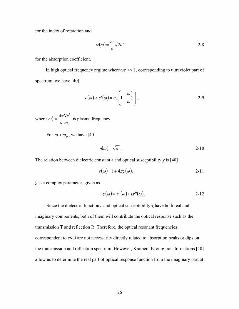
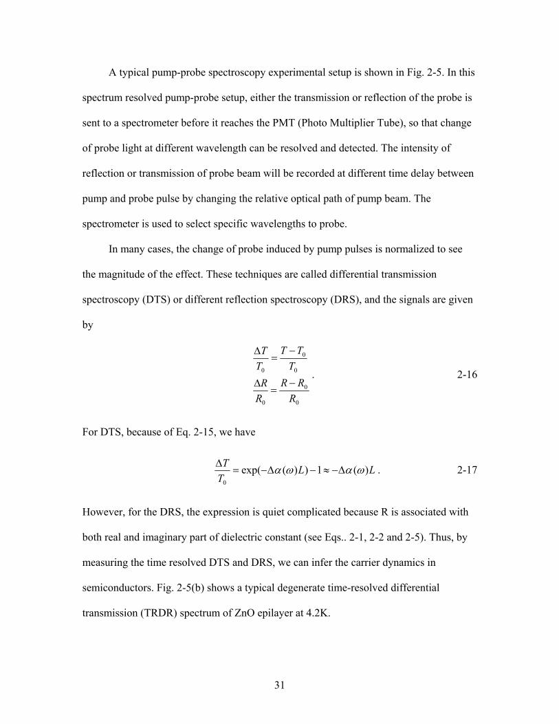
shown in Fig. 2-1. In this figure, we can clearly resolve several quantum states, which
will be interpreted in detail in Chapter 4. The dips in spectrum correspond to specific
interband transitions, which are the positions of excitonic states (see section 4.4). Using
transmission spectroscopy, we can directly mark the energy positions of Gaussian shape
absorption dips as excitonic states on the spectrum. However, care should be taken for the
band gap of substrate and barrier materials that they are high enough from the well
material band gap to avoid overwhelmed by the continuum states of the barrier and
substrate materials.
2.3.2 Reflection Spectroscopy
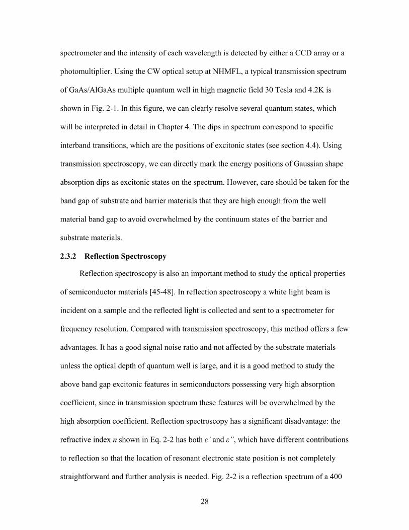
Reflection spectroscopy is also an important method to study the optical properties
of semiconductor materials [45-48]. In reflection spectroscopy a white light beam is
incident on a sample and the reflected light is collected and sent to a spectrometer for
frequency resolution. Compared with transmission spectroscopy, this method offers a few
advantages. It has a good signal noise ratio and not affected by the substrate materials
unless the optical depth of quantum well is large, and it is a good method to study the
above band gap excitonic features in semiconductors possessing very high absorption
coefficient, since in transmission spectrum these features will be overwhelmed by the
high absorption coefficient. Reflection spectroscopy has a significant disadvantage: the
refractive index n shown in Eq. 2-2 has both ε’ and ε”, which have different contributions
to reflection so that the location of resonant electronic state position is not completely
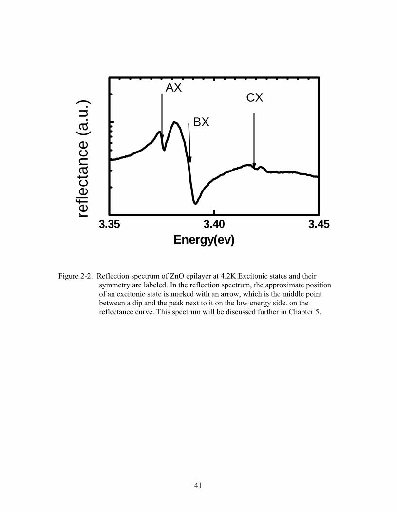
straightforward and further analysis is needed. Fig. 2-2 is a reflection spectrum of a 400
29
nm thick ZnO eplilayer at 4.2 K, the energy positions of electronic states are not clearly
resolved However, for a very good approximation, we can identify the states at the arrow
points shown on the figure as the energy positions of electronic states.
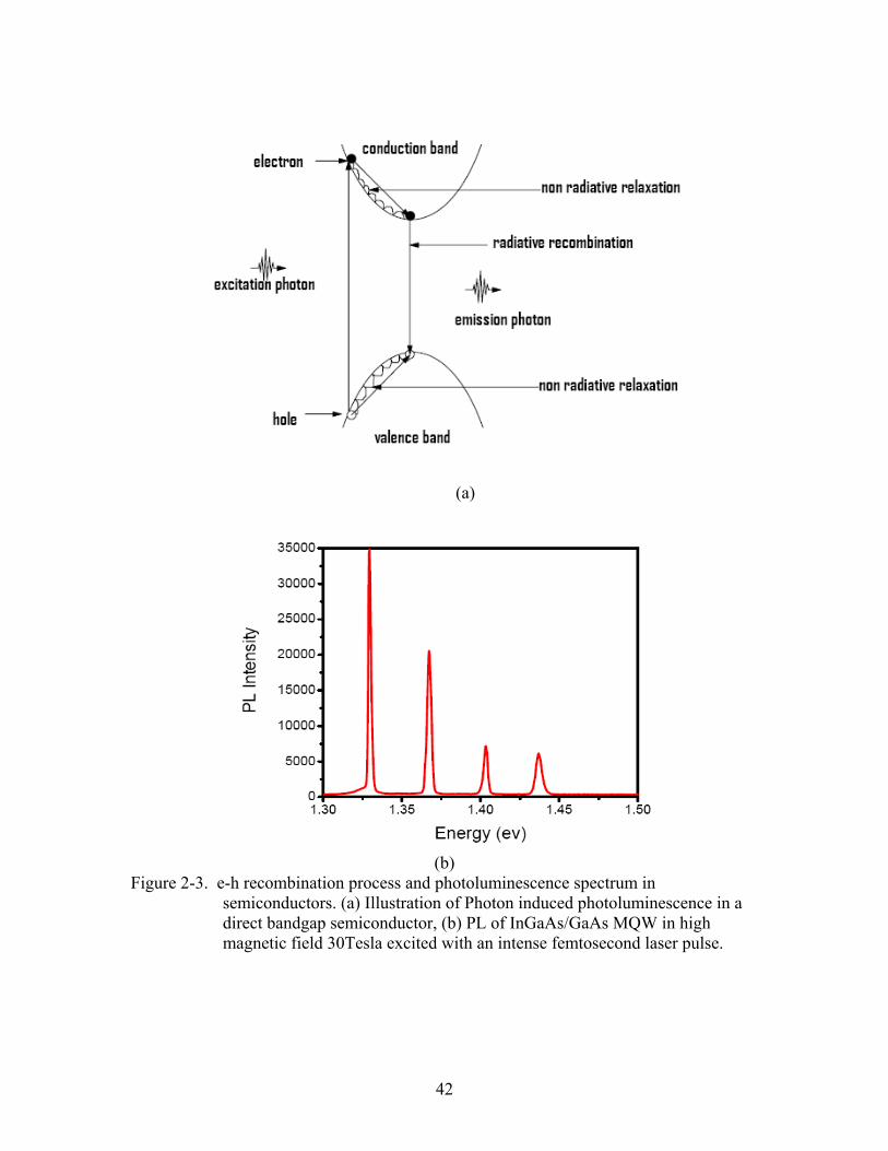
2.3.3 Photoluminescence (PL) Spectroscopy
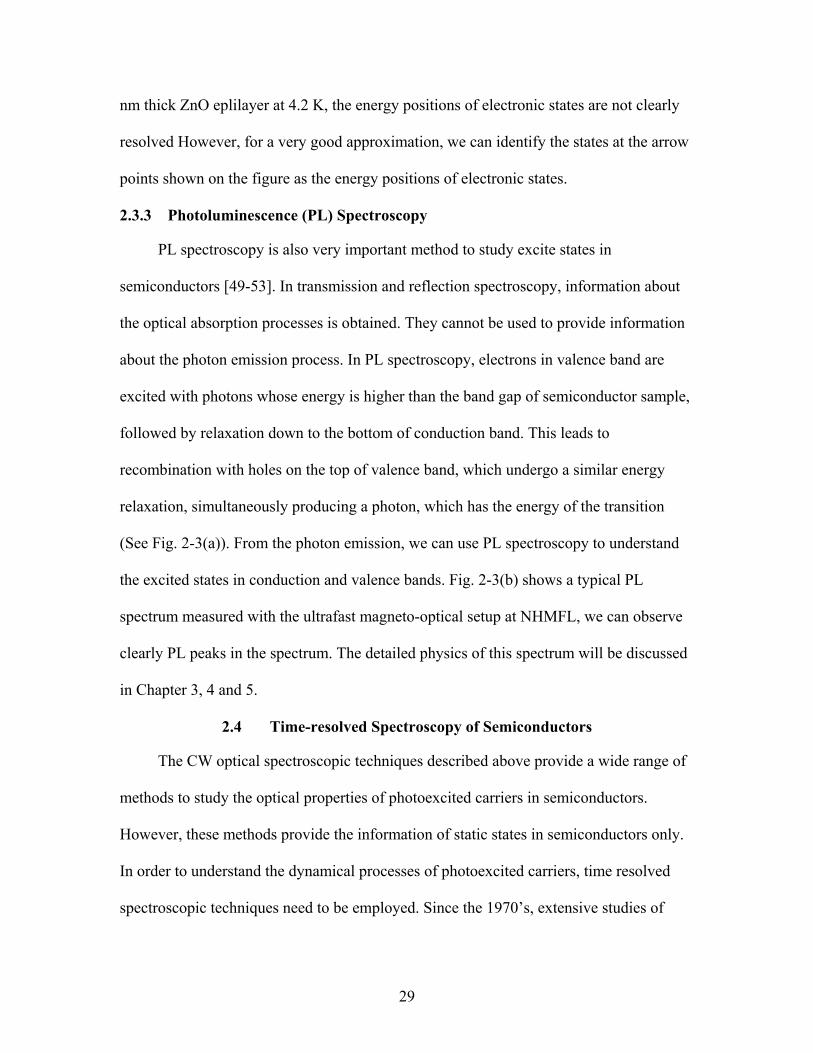
PL spectroscopy is also very important method to study excite states in
semiconductors [49-53]. In transmission and reflection spectroscopy, information about
the optical absorption processes is obtained. They cannot be used to provide information
about the photon emission process. In PL spectroscopy, electrons in valence band are
excited with photons whose energy is higher than the band gap of semiconductor sample,
followed by relaxation down to the bottom of conduction band. This leads to
recombination with holes on the top of valence band, which undergo a similar energy
relaxation, simultaneously producing a photon, which has the energy of the transition
(See Fig. 2-3(a)). From the photon emission, we can use PL spectroscopy to understand
the excited states in conduction and valence bands. Fig. 2-3(b) shows a typical PL
spectrum measured with the ultrafast magneto-optical setup at NHMFL, we can observe
clearly PL peaks in the spectrum. The detailed physics of this spectrum will be discussed
in Chapter 3, 4 and 5.
2.4 Time-resolved Spectroscopy of Semiconductors
The CW optical spectroscopic techniques described above provide a wide range of
methods to study the optical properties of photoexcited carriers in semiconductors.
However, these methods provide the information of static states in semiconductors only.
In order to understand the dynamical processes of photoexcited carriers, time resolved
spectroscopic techniques need to be employed. Since the 1970’s, extensive studies of
30
time resolved carrier dynamics in semiconductor have been reported [54-58], which have
opened a new research area for semiconductor optics.
The most common time resolved spectroscopic method used to investigate the
carrier dynamics in semiconductors are pump-probe spectroscopy and time-resolved
photoluminescence spectroscopy.
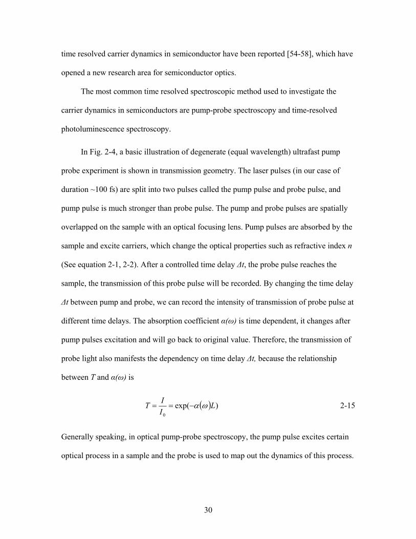
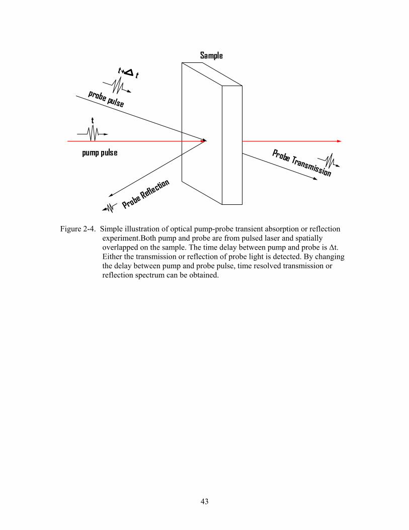
In Fig. 2-4, a basic illustration of degenerate (equal wavelength) ultrafast pump
probe experiment is shown in transmission geometry. The laser pulses (in our case of
duration ~100 fs) are split into two pulses called the pump pulse and probe pulse, and
pump pulse is much stronger than probe pulse. The pump and probe pulses are spatially
overlapped on the sample with an optical focusing lens. Pump pulses are absorbed by the
sample and excite carriers, which change the optical properties such as refractive index n
(See equation 2-1, 2-2). After a controlled time delay Δt, the probe pulse reaches the
sample, the transmission of this probe pulse will be recorded. By changing the time delay
Δt between pump and probe, we can record the intensity of transmission of probe pulse at
different time delays. The absorption coefficient α(ω) is time dependent, it changes after
pump pulses excitation and will go back to original value. Therefore, the transmission of
probe light also manifests the dependency on time delay Δt, because the relationship
between T and α(ω) is
( ) )exp(0
LIIT ωα−== 2-15
Generally speaking, in optical pump-probe spectroscopy, the pump pulse excites certain
optical process in a sample and the probe is used to map out the dynamics of this process.
31
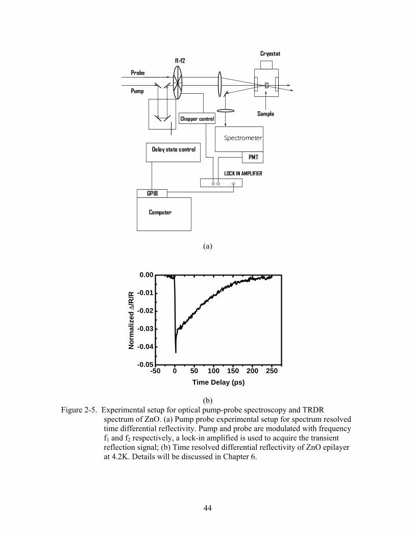
A typical pump-probe spectroscopy experimental setup is shown in Fig. 2-5. In this
spectrum resolved pump-probe setup, either the transmission or reflection of the probe is
sent to a spectrometer before it reaches the PMT (Photo Multiplier Tube), so that change
of probe light at different wavelength can be resolved and detected. The intensity of
reflection or transmission of probe beam will be recorded at different time delay between
pump and probe pulse by changing the relative optical path of pump beam. The
spectrometer is used to select specific wavelengths to probe.
In many cases, the change of probe induced by pump pulses is normalized to see
the magnitude of the effect. These techniques are called differential transmission
spectroscopy (DTS) or different reflection spectroscopy (DRS), and the signals are given
by
0
0
0
0
0
0
RRR
RR
TTT
TT
−=
Δ
−=
Δ
. 2-16
For DTS, because of Eq. 2-15, we have
LLTT )(1))(exp(0
ωαωα Δ−≈−Δ−=Δ . 2-17
However, for the DRS, the expression is quiet complicated because R is associated with
both real and imaginary part of dielectric constant (see Eqs.. 2-1, 2-2 and 2-5). Thus, by
measuring the time resolved DTS and DRS, we can infer the carrier dynamics in
semiconductors. Fig. 2-5(b) shows a typical degenerate time-resolved differential
transmission (TRDR) spectrum of ZnO epilayer at 4.2K.
32
Time-resolved differential transmission (TRDT) and reflection (TRDR) provide an
indirect method to study the carrier dynamics with very good time resolution (~100 fs
and shorter). However the mechanism of carrier recombination processes can not be
inferred, i.e. the radiative and nonradiative carrier recombination processes cannot be
distinguished from a pump-probe spectroscopy since both of them will contribute to
carrier recombination. To solve this problem, alternative techniques are required to
perform time-resolved study of the radiative processes. In time-resolved
photoluminescence, PL emitted from sample is sent to a streak camera, with which
temporal information of PL emission is acquired. The resolution of this method (~ps) is
not as high as pump-probe spectroscopy. The combination of pump-probe spectroscopy
and time resolved PL spectroscopy will give us a thorough understanding of photoexcited
carrier dynamics in semiconductors.
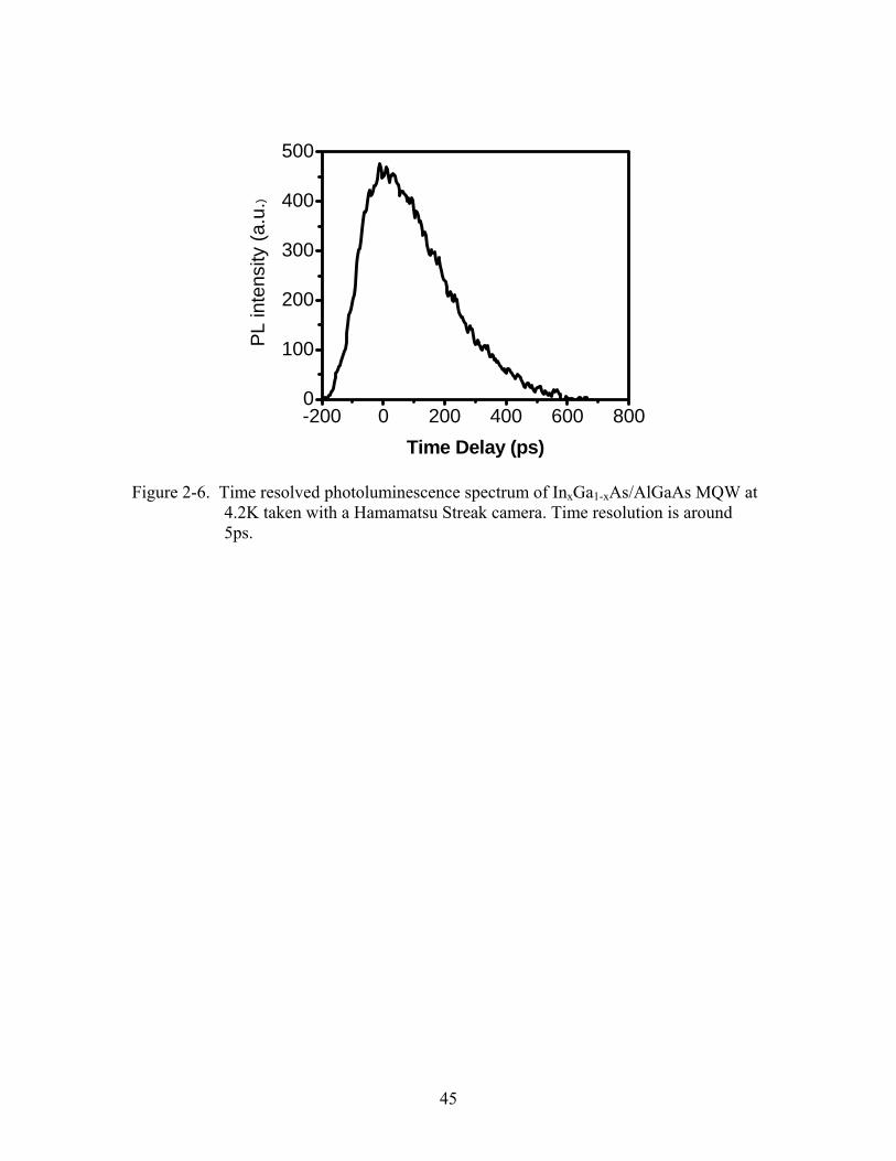
Fig. 2-6 shows a TRPL spectrum measured from InxGa1-xAs/AlGaAs MQW at
4.2K taken using a Hamamatsu streak camera. These time-resolved figures are typical
data we use in this thesis and the detailed physics will be discussed in the following
chapters.
2.5 CW Optical Experimental Capabilities at the NHMFL
Since the construction of the DC magnetic field facility at the National High
Magnetic Field Laboratory (NHMFL), there has been high demand for research in
magneto-optics, and many research projects have been accomplished with the well-
developed CW magneto-optical techniques that have been established [59-68]. In this
dissertation, many experiments were carried out to characterize InxGa1-xAs/GaAs MQW
sample by using the CW magneto optical setup at NHMFL in Tallahassee.

33
In order to reach high magnetic fields, we used a 31 Tesla resistive magnet in cell 5
at NHMFL. Fig.2-7 shows the schematic diagram of this magnet. This magnet is a
resistive magnet consists of a few hundreds of thin copper disks (Bitter disks). The Bitter
disks are connected electronically and electric current can flow through Bitter disks in a
spiral pattern. In Fig.2-7, we can see that there are four coils of Bitter disks in the magnet
housing. There are huge flows of electric current (~37KA) in the magnet coils when they
are in operation at full field, at the same time, cold water flows continuously through
holes punched on the Bitter disks to remove the huge amount of heat (~MW) generated
by the electric current.
In many magneto-optical experiments, low temperatures are usually required to
measure transmission, reflection and photoluminescence. Specially designed cryostats
and probes have been designed to work at liquid helium temperatures with these resistive
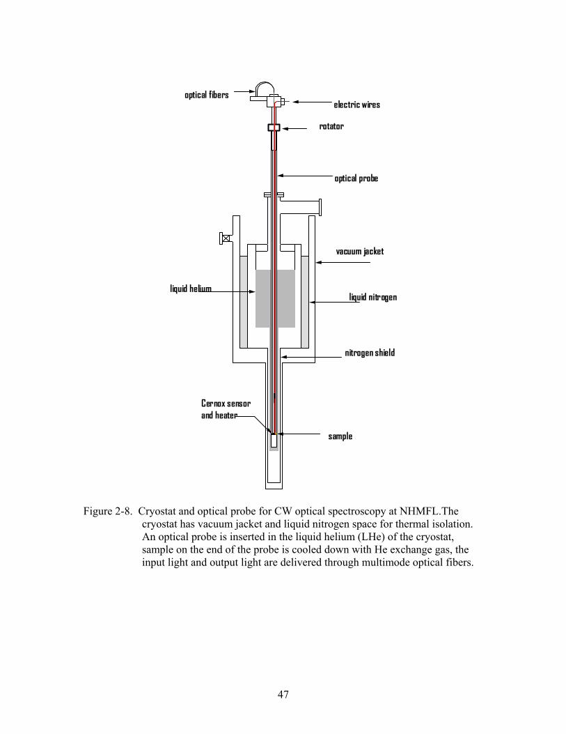
magnets with bore size around 50mm. The technical drawing of a cryostat and probes are
given in Fig. 2-8. This cryostat has a long tail, so that the probe/sample can reach the
position of highest magnetic field. In this cryostat, liquid helium is stored in the center
space and enclosed by liquid nitrogen or nitrogen shield and vacuum jacket, which
significantly reduce heat leaking into the helium reservoir. In Fig 2-8, an optical probe is
inserted into the liquid helium reservoir of this cryostat, and the sample inside the probe
is cooled down by back filling low-pressure helium exchange gas into probe. Light is
delivered to the sample through an optical fiber, and temperature of sample is measured
with a Cernox temperature sensor and controlled with a heater mounted on sample
mount.

34
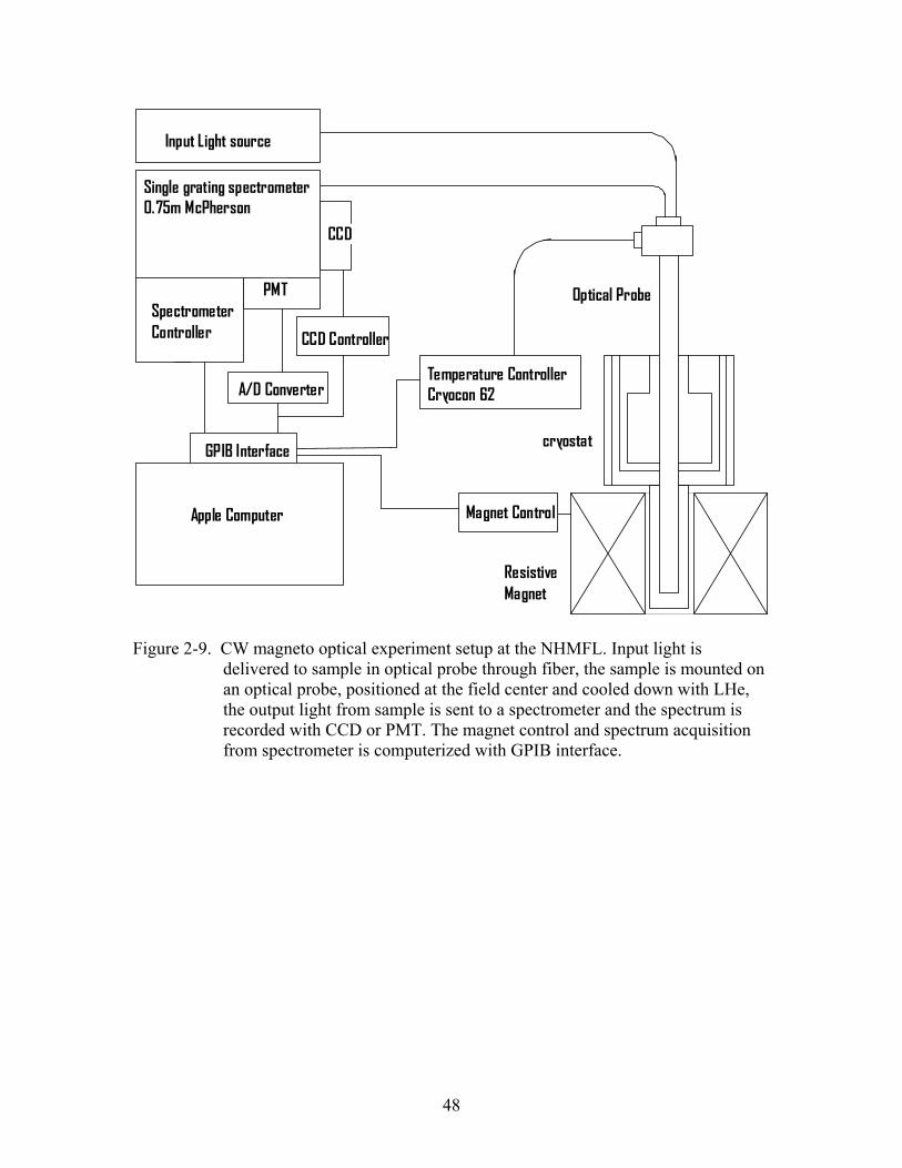
In Fig. 2-9, the layout of a typical CW magneto-optical experiment setup at
NHMFL is shown in a block diagram. An optical probe is inserted in the cryostat, which
is positioned on the top of a Bitter magnet. A Lakeshore temperature controller controls
the temperature of the sample via a sensor and heater co-located next to sample. The
input light and output signal light are delivered to sample and spectrometer respectively
through two optical fibers. In the case of transmission, reflection measurements, CW
white light sources (Tungsten or Xenon lamps) are used for input illumination while
lasers (He-Ne, He-Cd, Argon and Ti:Sapphire) are used as input excitation light for
photoluminescence (PL) experiments. The transmission, reflection and PL signal light are
collected with the output optical fiber mounted next to the sample and analyzed by a 0.75
m single-grating spectrometer (McPherson, Model 2075) equipped with single channel
photon counting electronics PMT as well as a multi-channel CCD detector. All of the
control units in this setup, including magnet controller, temperature controller,
spectrometer controller, PMT and CCD controller are managed by an Apple computer
through GPIB interfaces.
2.6 Development of Ultrafast Magneto-optical Spectroscopy at NHMFL
2.6.1 Introduction of Ultrafast Optics
With the existing CW magneto optical setup at NHMFL, many experiments have
been done successfully. However, there is still a drawback of this experimental setup –
time-resolved magneto-optical information can not be acquired due to large stretch effect
of multimode optical fibers, which expand the pulse width of ultrafast laser pulse
dramatically (from ~100fs to ~20ps) and results in a significant loss of time resolution. In
order to obtain time-resolved magneto-spectroscopy in high magnetic fields, a new

35
facility needs to be developed, which includes a new magnet, cryostat, probe as well as
new ultrafast light sources and detection methods.
2.6.2 Magnet and Cryogenics for Ultrafast Optics at NHMFL
Note that in a standard pump-probe experiment, while the excitation (pump) and
probe pulses must be delivered to the sample through free space to preserve the temporal
resolution, the collection of the light from the sample can be accomplished using standard
fibers.
To preserve the temporal duration of a femtosecond laser pulse before it reaches the
sample, direct optical propagation in free space is required. We also needed to modify
current cryostat so that it can be used on resistive magnet for ultrafast magneto optical
experiments. A technical drawing of modified optical cryostat is shown in Fig. 2-10. We
mount an optical window on the bottom of outer tail of the cryostat, open the bottom of
nitrogen shield, weld a copper sample mount right on the bottom of helium tail so that
samples can be cooled down with a cold sample mount. For the collection of light after
excitation of the sample, optical fibers positioned right on the top of sample are used to
deliver transmission or PL to spectrometer or detector. With this configuration, the
ultrafast laser pulse can reach the sample directly through resistive magnet bore and
optical window, while the sample can still be as cold as 10K (for more details see
appendix A).
In addition to resistive magnet, a superconducting magnet was also developed and
commissioned by us to carry out magneto-optical experiments, especially for the ultrafast
magneto-optics laboratory. We redesigned the cryostat for a 17 Tesla superconducting
magnet such that femtosecond laser pulses can be steered into the center magnet bore and

36
excite sample directly at field center. Fig 2-11 shows the section view of this
superconducting magnet. There is a stainless steel center bore welded on the cryostat and
going through the center of magnet. This bore isolates the sample chamber and helium
reservoir, which make it possible to do direct optics with this superconducting magnet.
The cold stainless steel bore is sealed with an optical window on the bottom and a
specially designed probe loading system on the top, shown in Fig. 2-12. With this probe
loading system, we can change sample without causing air leak into the center bore
merged in liquid helium. The sample on probe is cooled down with backfilling low-
pressure helium exchange gas in the center bore.
2.6.3 Ultrafast Light Sources
In addition to the development of cryogenics and magnet system, we also set up
several femtosecond pulse laser systems for time resolved magneto-spectroscopy. These
ultrafast laser systems include a Ti:Sapphire femtosecond oscillator, a Ti: Sapphire
chirped pulse amplifier (CPA) and an optical parametric amplifier (OPA).
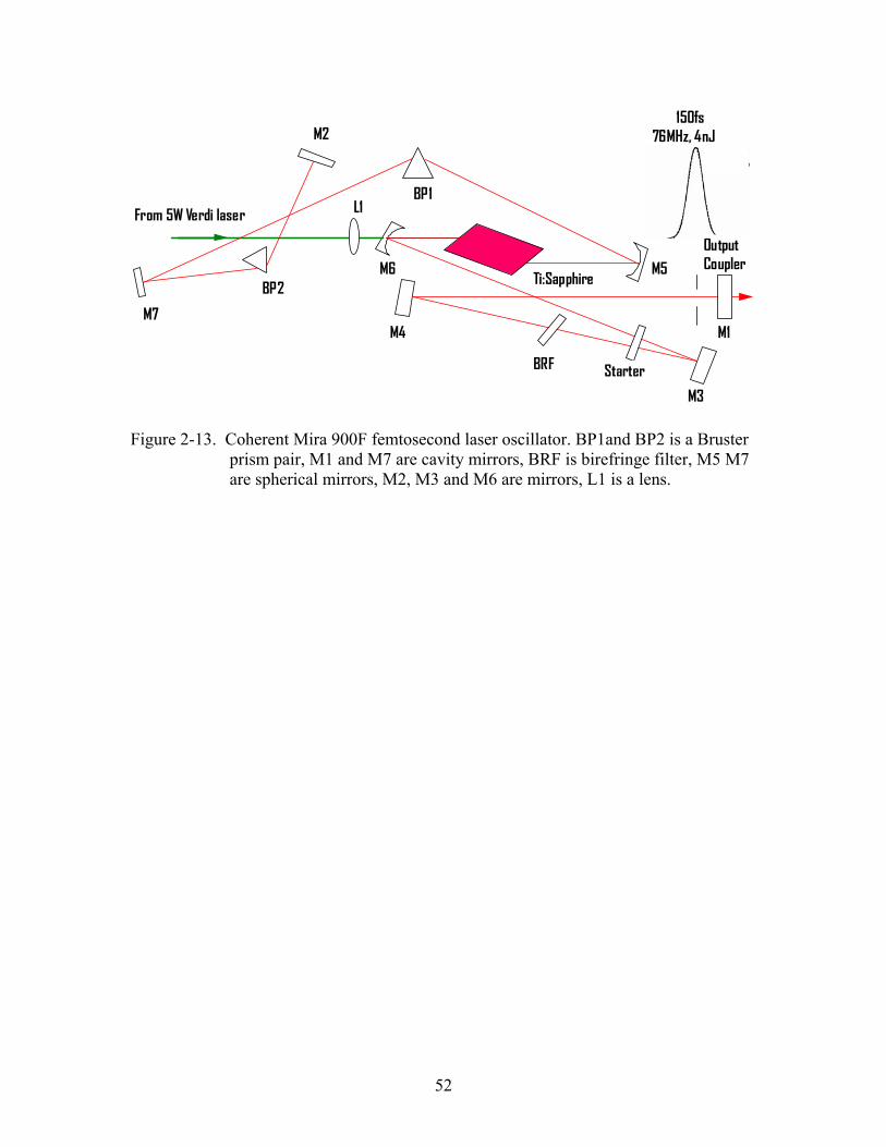
2.6.3.1 Ti:Sapphire femtosecond oscillator
Fig. 2-13 shows the schematic diagram of Coherent Mira 900 F femtosecond laser
system. In this laser system, a prism pair compensates dispersion caused by broad
bandwidth of laser emission. This passive mode locking ultrafast oscillator laser acquires
self-mode locking with Kerr Lens effect, and the shaker in the cavity works as a trigger to
initiate the mode locking. The pulse width of this ultrafast laser oscillator is around 150fs
and the energy per laser pulse is around 4nJ. This laser is tunable from 700 to 900 nm and
runs at 76MHz repetition rate. We use this ultrafast laser to get second harmonic
37
generation from BBO nonlinear crystal and carry out degenerate pump probe experiments
on ZnO semiconductors as described in Chapter 6.
2.6.3.2 Chirped pulse amplifier
In many optical experiments, strong ultrafast laser pulses (up to mJ per pulse) are
needed for either nonlinear effect like self phase modulation (white light generation) and
parametric amplification or for high carrier density generation in samples. Most of our
experiments were done with the Clark-MXR 2001 CPA. However, because of reliability
problems the Clark –MXR laser was later replaced by the Coherent laser in early 2007.
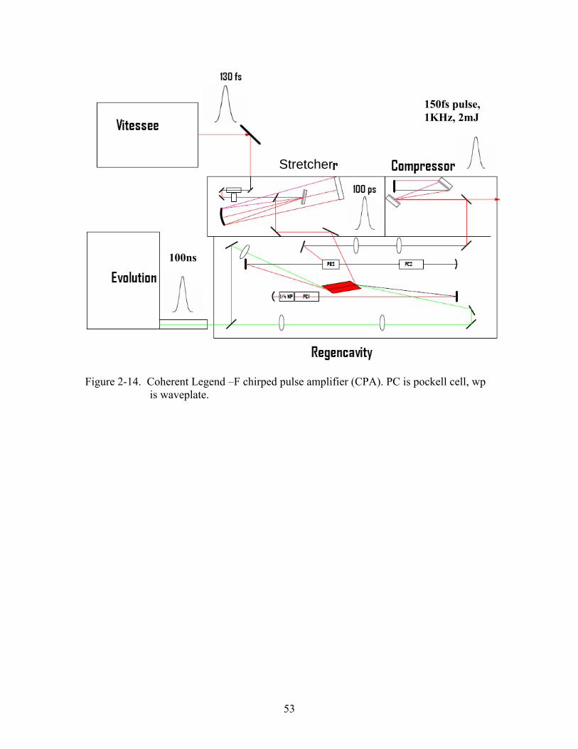
The current Coherent Legend-F chirped pulse amplifier (CPA) is set up in cell 3 at
DC facility for research in ultrafast magneto optics. Fig. 2-14 shows the schematic
diagram of this CPA femtosecond laser system. This CPA itself consists of three basic
components: a pulse stretcher, a regenerative amplifier cavity, and a pulse compressor
(see Fig.2-14). There are two external lasers for this CPA system, a Coherent Vitesse
oscillator (similar to the Mira described above), which generates a high repetition rate
ultrafast seed pulse train for amplification and an Evolution, which is a Q switch laser
used to pump Ti:Sapphire crystal inside regenerative amplifier cavity at a variable (but
typically 1 kHz) repetition rate with a 10mJ pulse. This CPA system functions in the
following manner. First, a 150 fs seed pulse train is generated in Vitessee laser and sent
into pulse stretcher. This seed pulse is stretched to approximately 100 ps, so that it will
not destroy the Ti:Sapphire crystal in regencavity as it get amplified. A Pockel cell (PC1
in Fig. 2-14) then picks off one pulse from the train within the regenerative amplifier
cavity for amplification. The pulse undergoes several roundtrips within the cavity and
through the Ti:Sapphire crystal which is prepumped with the Evolution laser and

38
experiences a total gain of approximately 106. Once the amplification of seed pulse
reaches its maximum (around 2 mJ per pulse), it is switched out of the regencavity by a
second Pockel cell (PC2 in Fig. 2-14) within the cavity. Finally, the amplified pulse
propagates through a grating compressor (see Fig.2-14) to compress the pulsewidth back
down to 150fs. At the output, we obtain 150fs laser pulses at a 1 kHz repetition rate and
2 mJ per pulse from this CPA system. As we discuss in Chapter 5, this laser is used to
study PL from high density of carriers in InxGa1-xAs/GaAs MQW in high magnetic field.
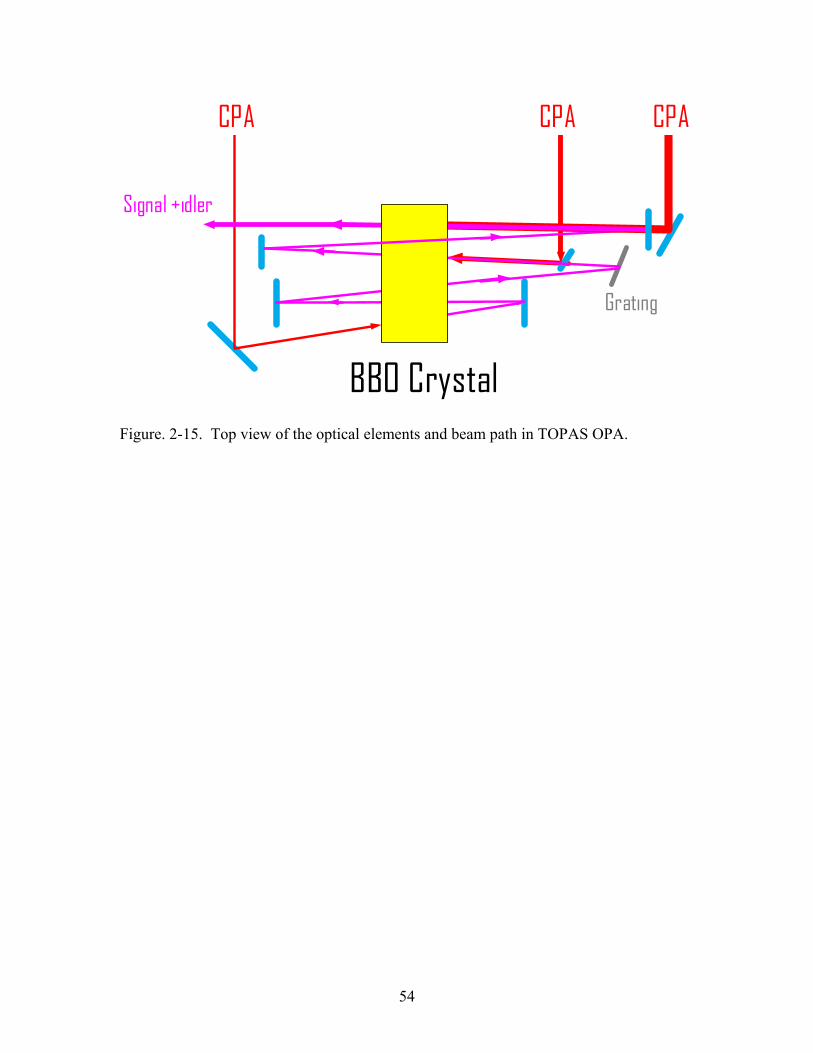
2.6.3.3 Optical parametric amplifier
The Ti:Sapphire oscillator and CPA laser can provide us with ultrafast pulse,
however, their wavelength ranges are limited. Therefore, an optical parametric amplifier
(OPA) is required to convert light to different wavelengths while preserving the short
duration of the pulses. Fig.2-15 shows the layout of a Quantronix OPA laser. This is a
five pass system in total. The first three passes of the pulse occur through a beta barium
borate (BBO) nonlinear optical crystal for frequency conversion, and a signal pulse (at
frequency ωsignal) and idler pulse (at frequency ωidler) are generated. In the forth and fifth
passes through the BBO crystal, signal and idler pulse are parametrically amplified with a
fraction of CPA pulse. The relation between fundamental CPA, signal and idler pulse is
given by
IdlersignalCPA ωωω += . 2-17
After parametric amplification by CPA pulse, the signal and idler pulses are then used to
generated ultrafast pulses at different wavelength through second harmonic generation
(SHG), ω=2ωsignal or 2ωidler, fourth harmonic generation (FHG), ω=4ωsignal or 4ωidler, and
different frequency mixing (DFG),

39
IdlersignalCPA ωωω −= . 2-18
The five nonlinearly optical processes mentioned above cover wavelength range from
300 nm to 20 μm.
2.6.3.4 Streak camera
In many cases, time-resolved photoluminescence is a very important method to
study the carrier dynamics since it provides a direct measurement of the radiative
emission of photons as carriers recombine in semiconductors. A picosecond streak
camera is the proper device to measure time resolved photoluminescence. Fig. 2-16
shows the operation principle of a streak camera. We are currently setting up a
Hamamatsu Streak Camera at the NHMFL ultrafast facility. In Fig.2-11 we can see that
conceptually, a PL pulse generated after excitation of a sample is steered into the slit and
then focused on a photocathode, where it is converted into an electron pulse of the same
duration. The electron pulse is then accelerated and passes through a very fast sweep
electrode, which is synchronized with the PL pulse, so that electrons at slightly different
time will be deflected at different angle by the AC high voltage and hit the CCD at
different position. Using this method, the temporal profile of a PL pulse is spatially
mapped on CCD in a spatial profile. By placing a spectrometer at the front end of the
streak camera, the PL can be spectrally and temporally resolved.
40
1300 1350 1400 1450 1500
e1hh2s
e2HH21se1lh
1s
e1hh1s
Tran
smis
sion
(a.u
.)
Energy (mev)
Figure 2-1. Transmission spectrum of InGaAs/GaAs MQW at 30 T and 4.2 K.The
energy position of each dip on transmission curve is correspondent to a magneto exciton state. Magneto-excitonic states are labeled according to the convention presented in Chapter 3.
41
3.35 3.40 3.45
refle
ctan
ce (a
.u.)
Energy(ev)
CX
BX
AX
Figure 2-2. Reflection spectrum of ZnO epilayer at 4.2K.Excitonic states and their
symmetry are labeled. In the reflection spectrum, the approximate position of an excitonic state is marked with an arrow, which is the middle point between a dip and the peak next to it on the low energy side. on the reflectance curve. This spectrum will be discussed further in Chapter 5.
42
(a)
(b)
Figure 2-3. e-h recombination process and photoluminescence spectrum in semiconductors. (a) Illustration of Photon induced photoluminescence in a direct bandgap semiconductor, (b) PL of InGaAs/GaAs MQW in high magnetic field 30Tesla excited with an intense femtosecond laser pulse.
43
Sample
pump pulse
probe pulse
t
t+ t
Probe Transmission
Probe Reflection
Figure 2-4. Simple illustration of optical pump-probe transient absorption or reflection
experiment.Both pump and probe are from pulsed laser and spatially overlapped on the sample. The time delay between pump and probe is Δt. Either the transmission or reflection of probe light is detected. By changing the delay between pump and probe pulse, time resolved transmission or reflection spectrum can be obtained.
44
Spectrometer
PMT
Probe
Pump
LOCK IN AMPLIFIER
Chopper control
Computer
GPIB
Delay state control
f1-f2Cryostat
Sample
(a)
-50 0 50 100 150 200 250-0.05
-0.04
-0.03
-0.02
-0.01
0.00
Nor
mal
ized
Δ/R
/R
Time Delay (ps)
(b) Figure 2-5. Experimental setup for optical pump-probe spectroscopy and TRDR
spectrum of ZnO. (a) Pump probe experimental setup for spectrum resolved time differential reflectivity. Pump and probe are modulated with frequency f1 and f2 respectively, a lock-in amplified is used to acquire the transient reflection signal; (b) Time resolved differential reflectivity of ZnO epilayer at 4.2K. Details will be discussed in Chapter 6.
45
-200 0 200 400 600 8000
100
200
300
400
500
PL in
tens
ity (a
.u.)
Time Delay (ps)
Figure 2-6. Time resolved photoluminescence spectrum of InxGa1-xAs/AlGaAs MQW at 4.2K taken with a Hamamatsu Streak camera. Time resolution is around 5ps.

46
Figure 2-7. Technical drawing of the 30 Tesla resistive magnet in cell 5 at NHMFL.
From National High Magnetic Field Laboratory, www.magnet.fsu.edu, side view of 31T / 32mm Resistive Magnet with Gradient Coil (Cell 5), date last accessed September, 2007
magnet bore
magnet housing
Bitter disks
47
vacuum jacket
liquid nitrogenliquid helium
nitrogen shield
optical probe
sample
Cernox sensor and heater
optical fiberselectric wires
rotator
Figure 2-8. Cryostat and optical probe for CW optical spectroscopy at NHMFL.The cryostat has vacuum jacket and liquid nitrogen space for thermal isolation. An optical probe is inserted in the liquid helium (LHe) of the cryostat, sample on the end of the probe is cooled down with He exchange gas, the input light and output light are delivered through multimode optical fibers.
48
Input Light source
Single grating spectrometer0.75m McPherson
CCD
PMT
Temperature ControllerCryocon 62
Magnet ControlApple Computer
Spectrometer Controller CCD Controller
A/D Converter
GPIB Interfacecryostat
Resistive Magnet
Optical Probe
Figure 2-9. CW magneto optical experiment setup at the NHMFL. Input light is delivered to sample in optical probe through fiber, the sample is mounted on an optical probe, positioned at the field center and cooled down with LHe, the output light from sample is sent to a spectrometer and the spectrum is recorded with CCD or PMT. The magnet control and spectrum acquisition from spectrometer is computerized with GPIB interface.

49
vacuum jacket
liquid nitrogenliquid helium
nitrogen shield
optical probe
sample
optical fibers
Bitter magnet
Cernox sensor and heater
CPA/OPA
Figure 2-10. Modified magneto optical cryostat for direct ultrafast optics. The optical
cryostat is positioned on the top of a resistive magnet and the sample is right at the field center. A sample mount is attached directly on the LHe tail of the cryostat, so that the sample can be cooled down. An optical window is mounted on the bottom of the outer tail of the cryostat, through which the ultrafast laser can reach the sample without being stretched significantly. The PL or probe light is delivered to detector and spectrometer through optical fiber.

50
vacuum jacket
LN2 spaceLN2 space
LHe reservor
superconducting manget
center bore
superconducting manget
optical window mount
KF flange connected to load lock KF flange
optical window
LHe reservor
He relife valve
N2 exhaust port
N2 shield
vacuum jacket
to vacuum pump
Figure 2-11. Technical drawing of the 17 Tesla superconducting magnet SCM3 in cell 3
at NHMFL. Stainless steel tubing is used as the center bore of this magnet, an optical widow is mounted on the bottom of the tubing, samples on probe are positioned in the center tubing. Ultrafast laser is steered in to the bore and excites samples without being stretched much.
Pulsed laser

51
cubic chamber for wires and fiber
9-pin connector forelectric wires fit through
cap for fiber fit through
flange connector
SS tubing 3/4"
Load lock
G-10 rod to mount wire SIP
G-10 ring
fiber
cernox sensorsample
double oring seal chamber
pump out port A
pump out port B
sample mount
To vacuum pump
valve A
valve B
connect to KF 50 on top of center tubing
Figure 2-12. Technical drawing of the special optical probe designed for
superconducting magnet 3 in cell 3 at the NHMFL. A load lock system is attached on the top part of this probe, the vacuum in the center bore of the magnet is not broken when loading and removing the probe from the cold magnet bore. Temperature of the sample is controlled with a Cernox sensor and electric heater. Ultrafast laser can reach the sample directly and the PL or probe light from sample is delivered outside with fibers.
Laser pulse
52
From 5W Verdi laserBP1
BP2
M2
M7
Ti:SapphireM5M6
L1
BRF Starter
M3
M1
150fs76MHz, 4nJ
OutputCoupler
M4
Figure 2-13. Coherent Mira 900F femtosecond laser oscillator. BP1and BP2 is a Bruster
prism pair, M1 and M7 are cavity mirrors, BRF is birefringe filter, M5 M7 are spherical mirrors, M2, M3 and M6 are mirrors, L1 is a lens.
53
Figure 2-14. Coherent Legend –F chirped pulse amplifier (CPA). PC is pockell cell, wp
is waveplate.
150fs pulse, 1KHz, 2mJ
100ns
Stretcher
54
BBO Crystal
CPA CPA CPA
Signal +idler
Grating
Figure. 2-15. Top view of the optical elements and beam path in TOPAS OPA.

55
t1t2
VTime varying high voltage
t2
t1
Incident light pulses
Photocathorde
Electrons
Streak Image
Streak Image
Time
Figure 2-16. Operation principle of a streak camera. The photocathorde converts light pulse t1 and t2 in to two electron pulses, the two electron pulses have different positions for streak images because the high voltage bias is time varying.
56
Bitter Magnet
Vitess
Legend CPA
Evolution
TOPASSOPA
Cryostat
Optical fiber
Optical fiber
Spetrometer
PMT
Box caraverager
Computer
Delay stage
Delay stage
parascope
CCD
Dichromirror
Dichromirror
SCM3
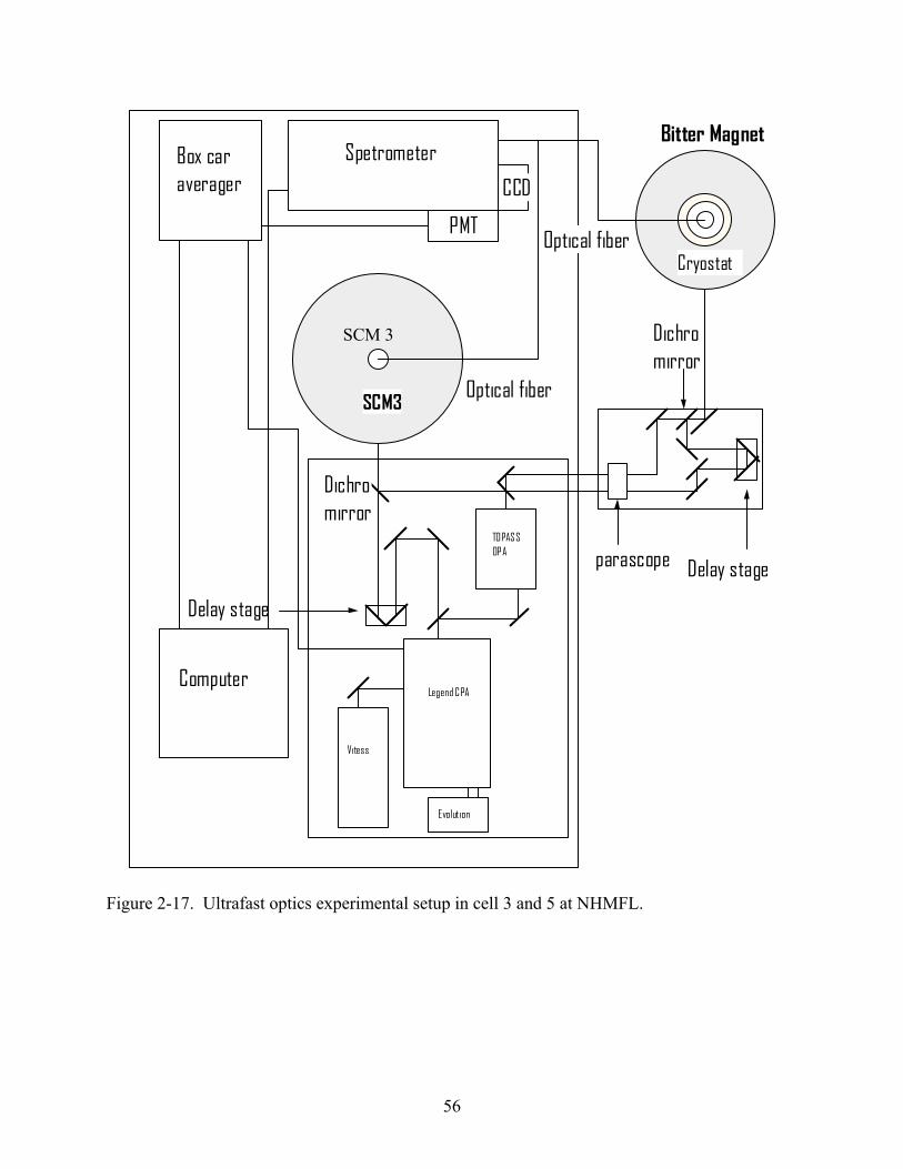
Figure 2-17. Ultrafast optics experimental setup in cell 3 and 5 at NHMFL.
SCM 3
57
CHAPTER 3 ELECTRONIC STATES OF SEMICONDUCTOR QUANTUM WELL IN MAGNETIC FIELD
3.1 Introduction
This chapter provides a background in the physics and optics of quantum confinement
induced by structural modifications (quantum wells) and strong magnetic fields. Optical and
electrical transport properties of semiconductor materials are determined by their electronic
states. A background in the fundamental band theory of semiconductors is necessary to
understand the magneto optical spectroscopy, specifically, of InxGa1-xAs/GaAs multiple quantum
wells, a typical III-V group semiconductor material, and ZnO (bulk, epilayer and nanorod),
typical II-VI group semiconductor material. Band structures of Wurzite symmetry (C6v) ZnO and
Zincblende symmetry (Td) InxGa1-xAs semiconductors are introduced.
In semiconductor quantum wells, carriers are confined in the two dimensions defined by
the barriers, and the electronic states have new characteristics with respect to bulk materials due
to quantum confinement. The exciton effect, energy states due to quantum confinement and
selection rules of optical transitions in quantum well are given in detail in this chapter.
In a high magnetic field oriented perpendicular to the plane of the quantum wells, further
confinement is introduced to a semiconductor quantum well, and the basic theory of magneto
optical process of semiconductor quantum well is given to understand the optical processes
related with interband Landau level transitions. Also, the density state of 3D, 2D and 1D
systems are given in this chapter.
3.2 Band Structure of Wurzite and Zinc Blend Structure Bulk Semiconductors
In a crystalline solid with N atoms, the electronic states of the N electrons make up
continuous energy bands separated by finite width band gaps. In a crystal, the electron

58
wavefuction and periodic potential of this crystal remain unchanged under translational
symmetry R (l, m, n), which can be described by the three primitive vectors: a, b and c as
ncmblanmlR ++=),,( ,
l, m, n are integers. Because of the translational symmetry, the electronic wave functions in a
crystal can be described with “Bloch function” [40]
)(1)(→
•→ →→
=Ψ rueN
r krki
k νν , 3-1
ν is the index of an electron energy band, k is a reciprocal lattice vector, N is the total number of
primitive cell unit in the crystal and u is a periodic function inside a primitive cell and has
translational symmetry
)()(→→
=+ ruRru νκνκ . 3-2
In equation 3-1, the Bloch function Ψνκ is normalized over the whole crystal and in Eq. 3-2,
)(ru kr
ν is a function normalized over the volume of a unit cell. The value of k is limited to the
Wigner-Seitz cell in reciprocal space, which is called “Brillouin Zone”.
Semiconductors are also a kind of solid crystal, which has a finite band gap between the
highest and fully occupied valence band and a lowest partially occupied (doped) or totally
unoccupied (undoped) conduction band. The band gap values and band structure of
semiconductors, which determine many optical and transport properties, are very important
parameters. The band gaps of semiconductors vary from near infrared (InAs 0.43eV) to
ultraviolet (ZnO 3.40eV). Among most of the III-V group semiconductors such as GaAs and
InAs, the typical structure is zinc-blende, while for the II-VI group semiconductors like GaN and
ZnO, the most common structure is the Wurzite structure.
In semiconductors, the Hamiltonian of an electron can be described as [71]:

59
CrystalS HHrVmkH +++=
→
0*
22
)(2h , 3-3
where k is the momentum of electron, m* is electron effective mass, V(r) is periodic potential in
semiconductor crystal, Hso is the spin and orbit interaction, and Hcrystal is the interaction between
electron and crystal field in an unit cell. Compared to the first two terms, the later two are
relatively small and can be treated as perturbation.
As the prototypical direct gap semiconductor, the first Brillouin zone and band structure of
GaAs (fcc structure) are given in Fig.3-1 (a). (We will be working with In0.2Ga0.8As in this
disseration, but the descriptions given for GaAs are applicable since GaAs and InAs have same
crystal structure.) At the center of the Brillouin zone, the point is labeled as Γ point (0, 0, 0). X
(1, 0, 0) on ky axis, and L (1/2, 1/2, 1/2) are also the fundamental points. The calculated
electronic band structure of bulk GaAs is shown in Fig. 3-1 (b). The conduction band in GaAs
has absolute minimum value at the Γ-point and two local minima at the L-point and X-point,
which are referred as L valley and X valley. The conduction band of GaAs does not split since it
is a s-like nondegenerate band, while the valence band split into three bands: heavy-hole, light-
hole and split-off bands since they are p-like three folds degenerate [71]. The degeneracy
between split-off (J=1/2) and heavy-hole and light-hole (J=3/2) is lifted due to the interaction
(Hso) between electron spin (s=±1/2) and angular momentum (l=±1 for p-like electron).
However, at the Γ-point, the degeneracies of light-hole and heavy-hole subbands are not lifted
because of the high cubic symmetry (Td point group) of the GaAs cell (Hcrystal=0).
In a Wurzite structure semiconductor such as GaN and ZnO, the first Brillouin zone and
bandstructure are quite different from the zinc-blende structure. Fig 3-2 (a) and (b) present the
first Brillouin zone and band structure of a zinc-blende structure GaN semiconductor. At the Γ-
point, the valence band of Wurzite structure semiconductors split into three subbands (heavy
60
hole, light hole, and split-off) due to the hexagonal (C6v point group) symmetry of GaN crystal
cell, which gives an additional perturbation part of Hcrystal ≠ 0 and lifts the degeneracy.
In the optical transitions in semiconductors, a photon is either absorbed or emitted. This is
based on electron transitions between the top of valence band and bottom of conduction band.
The selection rule for this optical transition is Δk = 0, which expresses the momentum
conservation of crystal. Compared to the crystal momentum, the momentum of photon is very
small and can be neglected.
For direct bandgap semiconductors such as GaAs and ZnO, the valence band absolute
maximum and the conduction band absolute minimum occur at Γ-point, the center of Brillouin
zone, where interband and intraband (inter-subband) transitions are observed without phonon
emission. The optical transitions from other valley (X or L valley) in conduction band to Γ-point
of the valence band must be accompanied by the emission of a phonon to conserve the crystal
momentum.
3.3 Selection Rules
In Kane model [72], since in all the II-VI and III-V group semiconductors the chemical
bond are formed with outer shell electrons nsnp, the wave functions of hybridized s-like band
and p-like bands can be represented using 8 band edge Bloch functions (u0, u1,…, u8)
|S↑›,|X↑›,|Y↑›,|Z↑› and |S↓›,|X↓›, |Y↓›, |Z↓›. However, after the spin orbit interaction Hso is
considered, a new linear combination of these functions can be formed. In the new functions,
J=L+S and Jz are good quantum numbers and H can be diagonalized. The new Bloch functions
basis set [71] is given in Table 3-1. They are taken as a basis set in a Kane model calculation
[72].

61
The optical transitions between conduction band and valence band due to electro dipole
transitions in semiconductor are described by the transition matrix element [71]
∫→→
Ψ⋅Ψ= rdpM ifif
^* ε . 3-4
where ^ε is the optical polarization unit vector and p
→
is the electron momentum operator. Using
the Bloch functions (Eq. 3-2), Mif can be expressed approximately as [71]:
M u p u f f d r u u f p f d rif f i f i f i f i= ⋅ ⋅ ⋅ + ⋅ ⋅→
∗→
∗→ →
∫ ∫ε εν ν ν ν
^ ^, 3-5
where u fν and u iν are the wave functions for the initial and final state(see Eq.3-1),
fN
k r= •→ →1 exp( ) is the envelop function and u uf i f iν ν ν νδ= , , the transition matrix is mainly
determined by first term in Eq.3-5.
The absolute values of the transition matrix elements nupS→
⋅^ε are listed in table 3-2,
where S is the conduction band wavefunction and un is the valence band wavefunction, x, y, and
z are the propagation direction of light, εx, εy and εz are light polarization
andΡ =−
=−
=−i
mS p X i
mS p Y i
mS p z
ex
ey
ez .
3.4 Quantum Well Confinement
In this thesis, we have focused our study on type I quantum well structure described in
chapter 1. The Bloch wave function of an electron or hole confined in the quantum well with
periodic potential V(z) is described as [41]
)()(→
• ⊥→→
=Ψ ruze rkiνκνκ χ , 3-6
62
here k is the electron wave vector in xy-plane and χ( )z is an envelop function along the z
direction, in which the quantum well is grown. We can separate the wave function (Eq. 3-6) into
xy and z directions. In the z direction, we have
)()()(2 2
2
*
2
zEzzVdzd
mi
nχχ =⎟⎟⎠
⎞⎜⎜⎝
⎛+−
h . 3-7
The eigenvalues En of this equation 3-7 are the energies of different quantum confined
subbands. A schematic diagram of the confinement subbands in a type I quantum well is shown
in figure 3-3.
For the states in the xy plane, if we use parabolic bands for kx and ky, the carrier energies in
the quantum wells are given by:
E Em
k kn x y= + +∗
h22 2
2( ) . 3-8
The Bloch wave function (Eq. 3-6) for a quantum state labeled by n can be expressed as
⊥→→⋅==Ψ rki
nnnn ezufu )(χνν ,
here, →
k and r⊥→
are the 2D electron wave vector and position vectors in the xy-plane.
With the envelope functions χ( )z , we can derive the selection rules of the envelope
function from equation 3-5,
∫∫ ⊥−= dzzzdreff mn
kkiif
fi
)()(*)( χχ . 3-9
The first term shows that the optical transition is allowed when the electron momentum k is
conserved
if kk = .
The second term gives us the selection rule for transition between two different subbands [41]

63
n-m=even.
However, the transitions corresponding to n-m=0 are far stronger than n-m=2, 4, 6… [41]. The
optical transitions processes correspondent to n-m=0 are shown in Fig. 3-3.
3.5 Density of States in Bulk Semiconductor and Semiconductor Nanostructures
A consideration of the density of states is very important for understanding the optical
response of semiconductors. It expresses how many states are available in the system in the
energy interval between ε and ε+dε; the maximum number of carriers is reached when all the
density of states is occupied up to Fermi level. This will become particularly important for
understanding the superfluorescence experiments in Chapter 5. The density of states in a bulk
semiconductor is given as [41]
g mD32
02
32 1
212
2( )επ
ε=⎛⎝⎜
⎞⎠⎟
∗
h. 3-10a
In a 2D semiconductor quantum well, the carriers are confined within the well width, so the
density of states is described as [41]:
g mDj
j
22 0( ) ( )ε
πθ ε ε= −∑
h. j= 1, 2, 3···. 3-10b
Here, j is the index of quantum confined states and θ ε ε( )− j is the step function.
For a 1D system, the density of states is given by [41]:
g mD r
j jj j x zx z
12
121
21( )
,
επ ε ε ε
= ⎛⎝⎜
⎞⎠⎟ − −∑
h. 3-10c
Here, jx and jz are index of quantum confinement states on z and x direction.
If all the 3 dimensions are quantum-confined for a free carrier, we have a quasi 0D system,
and the zero dimensional carrier density of states is given by [41]
( )g Dj
j
0 2( )ε δ ε ε= −∑ . 3-10d
64
Here, ε j is the energy of the jth quantum confinement state and ( )δ ε ε− j is the Dirac delta
function.
The density of states curves for 3D, 2D, 1D and 0D system are plotted in Fig.3-4. We can
see that for 3D and 2D systems, the density of states is continuous, while in 1D and 0D, the
continuums collapse and the density of state get discrete and turn into δ function.
3.6 Magnetic Field Effect on 2D Electron Hole Gas in Semiconductor Quantum Well
In a type I semiconductor quantum well such as InxGaAs1-x/GaAs, electrons and holes are
confined in a potential well defined by the xy-plane. In the presence of magnetic field along the z
direction, an additional quantum confinement is applied to the electrons and holes in the xy-
plane. The Hamiltonian of an electron in a quantum well in the presence of magnetic field along
z direction is given by [71]
Hm
p e Ac
V z= − +→
→
12
2( ) ( ) , 3-11
where A xB→
= ( , , )0 0 is the vector potential and V(z) is the quantum well confinement potential.
We can separate the electron wave function into xy-plane component and z direction component,
so the wavefunction Ψ can be written in the form
)(),(),,( zfyxhzyx =Ψ .
Using this wave function, the Schrödinger equation can be separated in two independent
equations:
(I) In z-direction (QW growth direction), we have
)()()(2 2
2
*
2
zfEzfzVdzd
mi
n=⎟⎟⎠
⎞⎜⎜⎝
⎛+−
h . 3-12
65
This is referred to type I semiconductor quantum well confinement and discussed earlier (see
Eqs.3-7, 3-8 and 3-9).
(II) In xy- plane (quantum well plane), we can modify the Schrödinger equation.
Setting )'(),( )( xeyxh yiyk ϕ= , Eq. 3-12 can be modified into [71]
)'()'(2
''2 *
222
2
2
*
2
xExm
xBedxd
m xyϕϕ =⎥⎦
⎤⎢⎣
⎡+
− h ,. 3-13
where x xk
Bey'= +
h. This is a typical Schrödinger equation for harmonic oscillators and the
solution is well known. The energy of this xy-plane motion is given by [71]
E Nxy c= +⎛⎝⎜
⎞⎠⎟
12hω N=0, 1, 2...
where ωcBem c
= ∗ is called cyclotron frequency. The quantum states corresponding to the
harmonic oscillator energy states are known as Landau levels.
The total energy including both z- and xy in-plane contributions is
E E Nn c= + +⎛⎝⎜
⎞⎠⎟
12hω
There are some important lengths and densities that define quantum wells in magnetic
fields. The magnetic length lc is defined aseB
clch
= . The degeneracy of a Landau level is 2eBh ,
where the factor of 2 comes from electron (hole) spin. Typical Landau levels evolve from
electronic quantum confinement energy levels in a quantum well are shown in figure 3-5. The
crossing or anti-crossing effect between 3rd Landau level evolves from E1 and the 1st Landau
level evolves from E2 state is shown. The crossing or anti-crossing effect depends on the
symmetry properties of wave function of the states and the perturbation at the intersecting point.
For a particular magnetic field, the number of electrons populating a LL is finite. The
electron density on a filly filled Landau level at a magnetic field is given by [71]

66
n eBhe = .
The filling factor ν is defined as
eBnh
nn
e
==ν .
Physically ν/2 at any magnetic field gives the number of fully occupied Landau levels. And
again, the factor of ½ comes about because each Landau level has two spin states.
3.7 Excitons and Excitons in Magnetic Field
3.7.1 Excitons
As discussed in Chapter 1, an exciton is a pair of an electron and a hole due to the
Coulomb interaction between them, and its energy states are very similar to a hydrogen atom.
Therefore, the exciton energy levels are expressed as
2
*
222
*4
2 nR
nmeE excition
n ==εh
, 3-14
where ε is the dielectric constant of semiconductor material, m* is the reduced effective mass of
an exciton, n=1, 2, 3…, and 22
*4*
2 εh
meR = [41] is called the effective Rydberg energy and
2*
2*
emaB
hε= is an effective exciton Bohr radius. Similar to the hydrogen system, for a given
quantum number n, the degenerate state has fine structures due to angular momentum l=0, 1, 2,
3…. The fine structure of this exciton is also labeled as 1s, 2s, 2p…
In semiconductor quantum wells, the exciton binding energy increases with respect to bulk
semiconductors because the electrons and hole at the bottom of conduction band and holes at the
top of valence band, which form the excitons, are confined in the same well and their wave
function overlap is larger than in the corresponding bulk material. Therefore, the exciton binding
energy depends strongly on barrier height and the well width.

67
Unlike the exciton binding energy for the 3D bulk case given in equation 3-14, in a
quantum well with well width less than the exciton diameter 2aB*, the confinement has a
significant effect on excitons—one layer of electrons and holes gas are confined in a two
dimensional plane. In quantum wells with extremely narrow well widths, the exciton binding
energy are given by [41]
2
*2
)21( +
=n
RE DExcition
. 3-15
So, in the 2D case, the ground state binding energy of an exciton is 4R*, which is four times that
of the 3D bulk semiconductor [73-76].
3.7.2 Magneto –excitons
In the presence of magnetic field, the excitons in semiconductors are called magneto-
excitons. Due to the existing magnetic field, the electron and holes start to orbit with respect to
each other, and the orbit shrinks if the magnetic field increases. We can expect that the
hydrogen-like exciton wave functions diminish in radius with increasing magnetic field.
The Hamiltonian of an exciton in a quantum well in the presence of magnetic field
perpendicular to the well layer can be depicted as:
H H H e
r re h
e h
= + −−
→ →
2
ε. 3-16
The first two terms are the Hamiltonian of electron and hole in magnetic field, and the third term
is the Coulomb interaction, which depends on the separation between electron and hole in an
exciton. The first two terms can be expressed as [71]:
Hm
p e A r V re he h
e h e h,,
, ,( ( )) ( )= ± +→ → → →1
22 , 3-17

68
where A r B→ → →
= ×12
( ) is the vector potential from magnetic field.
Due to the presence of the potential e
r re h
2
ε→ →
−, we cannot separate the Hamiltonian in Eq.3-
16 and the wave function into two parts for z direction and xy-plane to get an analytical solution.
However, if perturbation theory is used to treat the exciton ground state in the presence of
an external magnetic field, we can consider the effect of low magnetic field as small
perturbation. The perturbation caused by magnetic field can be described as [71]:
23*22
422*
421)( B
mecDRBEground
hεγ =≈Δ , 3-18
where γ is a dimensionless effective magnetic field in the form of *Rcω
γh
= , which is the ratio of
cyclotron energy and excition binding energy, ω ω ωc ce cheB
m c= + = ∗( ) is the combination of
electron and hole cyclotron energy and D is the dimensionality parameter for the excitons.
Equation 3-18 is often called “diamagnetic shift of exciton” and only valid for γ<1 [71].
In the case of high magnetic field limit, where the magnetic field effect is larger than
exciton effect and γ>>1, the magneto-exciton is more similar to a free electron hole pair in
magnetic field, and the binding energy Ry* is considered only as small perturbation (See Eq. 3-
16). Therefore, in high magnetic fields, the energy shift due to magnetic field is given by:
ΔE Bground c( ) = 12hω .
For a GaAs semiconductor quantum well, where R* is 5.83 meV [77], the value of γ is
around 5 T. This is a significant point--if we want to study the optical magneto-exctions in GaAs,

69
it is necessary to use high magnetic fields in excess of 20 T, since the magnetic field effect is 4
times larger than the Coulomb effect.
Figure3-6 shows the calculation results of free electron hole transition energy and exciton
energy of InxGaAs1-xGaAs (including the band gap Eg) in magnetic field. The solid line are
excitonic, which includes the Coulomb interaction between electron and hole pairs that populate
at different Landau levels, while the dashed line are Landau energy levels correspondent to free
electron and hole populate on different Landau levels.
Using this theoretical basis, we turn now to a study of the magneto-optical properties of
excitons in In0.2Ga0.8As/GaAs quantum wells with the goal of understanding emission from
highly excited quantum wells in high magnetic fields.

70
Table 3-1. Periodic parts of Bloch functions in semiconductors Quantum number Wavefunction u1 |s, 1
2, 12
› i |S↑›
u2 |s, 12
, - 12
› i |S↓›
u3 |p, 32
, 32
› 12
|(X+iY) ↑›
u4 |p, 32
, - 32
› 12
|(X+iY) ↓›
u5 |p, 32
, 12
› 16
|(X+iY) ↓›- 23
|Z ↑›
u6 |p, 32
, - 12
› - 16
|(X+iY) ↑›- 23
|Z ↓›
u7 |p, 12
, 12
› 13
|(X+iY) ↓›+ 13
|Z ↑›
u8 |p, 12
, - 12
› - 13
|(X-iY) ↑›+ 13
|Z ↓›
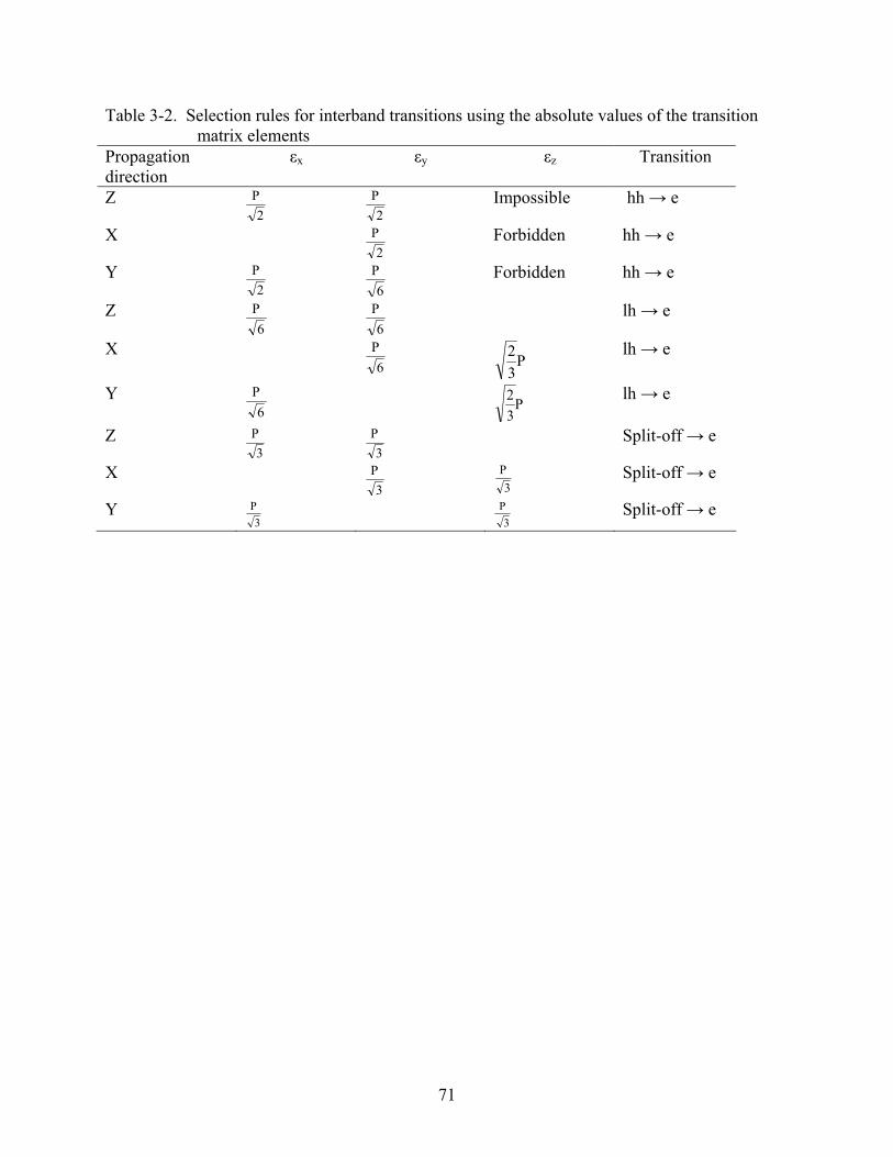
71
Table 3-2. Selection rules for interband transitions using the absolute values of the transition matrix elements
Propagation direction
εx εy εz Transition
Z Ρ2
Ρ2
Impossible hh → e
X Ρ2
Forbidden hh → e
Y Ρ2
Ρ6
Forbidden hh → e
Z Ρ6
Ρ6
lh → e
X Ρ6
23Ρ lh → e
Y Ρ6
23Ρ lh → e
Z Ρ3
Ρ3
Split-off → e
X Ρ3
Ρ3
Split-off → e
Y Ρ3
Ρ3
Split-off → e
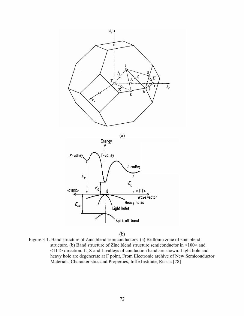
72
(a)
(b) Figure 3-1. Band structure of Zinc blend semiconductors. (a) Brillouin zone of zinc blend
structure. (b) Band structure of Zinc blend structure semiconductor in <100> and <111> direction. Γ, X and L valleys of conduction band are shown. Light hole and heavy hole are degenerate at Γ point. From Electronic archive of New Semiconductor Materials, Characteristics and Properties, Ioffe Institute, Russia [78]
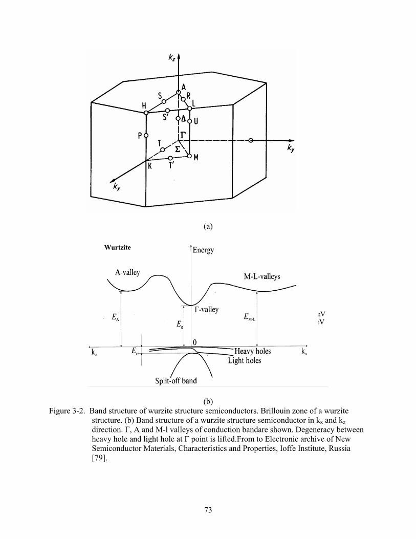
73
(a)
(b) Figure 3-2. Band structure of wurzite structure semiconductors. Brillouin zone of a wurzite
structure. (b) Band structure of a wurzite structure semiconductor in kx and kz direction. Γ, A and M-l valleys of conduction bandare shown. Degeneracy between heavy hole and light hole at Γ point is lifted.From to Electronic archive of New Semiconductor Materials, Characteristics and Properties, Ioffe Institute, Russia [79].
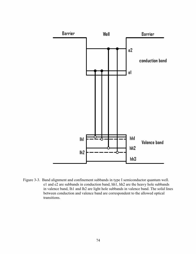
74
Figure 3-3. Band alignment and confinement subbands in type I semiconductor quantum well.
e1 and e2 are subbands in conduction band, hh1, hh2 are the heavy hole subbands in valence band, lh1 and lh2 are light hole subbands in valence band. The solid lines between conduction and valence band are correspondent to the allowed optical transitions.
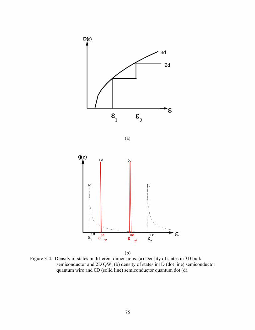
75
ε2
ε1
D(ε)
ε
3d
2d
(a)
ε12
dε0d1' ε0d
2'ε1d
1
g(ε)
ε
1d 1d
0d 0d
(b)
Figure 3-4. Density of states in different dimensions. (a) Density of states in 3D bulk semiconductor and 2D QW; (b) density of states in1D (dot line) semiconductor quantum wire and 0D (solid line) semiconductor quantum dot (d).
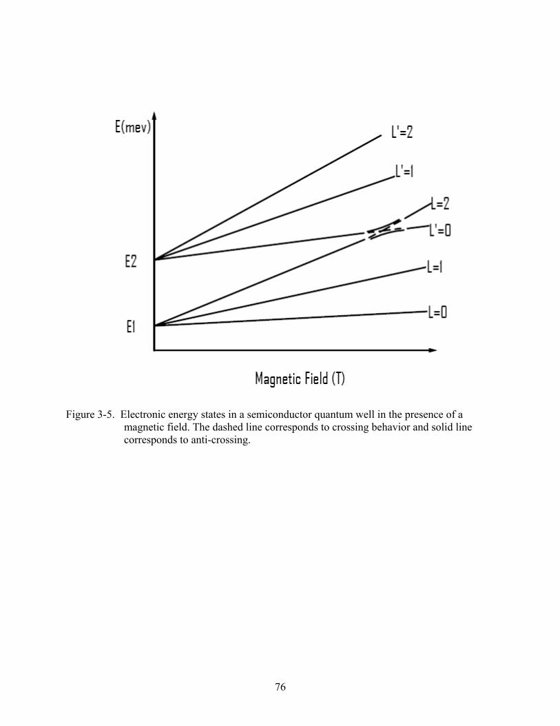
76
Figure 3-5. Electronic energy states in a semiconductor quantum well in the presence of a
magnetic field. The dashed line corresponds to crossing behavior and solid line corresponds to anti-crossing.

77
Figure 3-6. Calculation of free electron hole pair energy (dash line) and magneto exciton
energy(solid line) of InxGa1-xAs/GaAs QW as function of magnetic field. s, p, d. f are different magneto excitionic states. Solid lines are for the e-h pair with consideration of Coulomb effect and dash lines are for the e-h pair without considering Coulomb interaction. Reprint with permission from T. Ando et al., Phys. Rev. B 38, 6015-6030, (1988), figure 7 on page 6022.
78
CHAPTER 4 MAGNETO-PHOTOLUMINESCENCE IN INGAAS QWS IN HIGH MAGNETIC FIELDS
4.1 Background
Optical phenomena arising from interband and intraband transitions in 2D electron-hole
gases in III-V semiconductor quantum well have been studied intensively and extensively in
theory and experiments during the past several decades owing to the intense interest in the
physics of low dimension system and their potential applications [81].
In a magnetic field, the quantum-confined states in the conduction and valences band split
into different Landau levels, resulting in electrons and holes populating different Landau levels,
thus, the interband Landau level transitions will dominate optical transitions in magnetic fields.
By observing and analyzing inter-LL optical transitions, we can study the optical transitions of
2D electron hole gas such that detailed information about the conduction and valence band
structures, carrier effective mass and carrier interactions between different Landau levels (such
as crossing and anti-crossing) can be acquired [82-84]. This work will serve as a background to
the next chapter on the nature of light emission from dense magneto-plasmas in quantum wells.
Using relatively weak light sources such as tungsten and xenon lamps, we can measure the
absorption spectrum of optical transitions from valence band Landau levels to conduction band
Landau levels in semiconductor QWs in magnetic fields and determine the energy peaks of each
inter-Landau level transition. In the absorption spectrum, these optical transitions are still
predominantly excitonic, since the separation between two electron hole pairs is relatively larger
than the exciton Bohr radius ( d aexciton>> ), so that the Coulomb interaction between electron and
hole in a exciton system are not screened.
PL due to recombination of electrons on a conduction Landau level with holes on a valence
band Landau level is necessary to study the Landau level physics of magneto-excitons (at low

79
densities) or magneto-plasmas (at high densities). In this case, CW excitation (for example, with
a He-Ne laser) is not sufficient since it cannot create a large number of carriers to populate in
higher Landau levels; the only photon emission channel is due to the transition lowest electron
Landau level to highest hole Landau level. Therefore, pulsed lasers such as Q-switched or mode
locked lasers are needed to generate a sufficiently high carrier density so that interband
transitions due to higher Landau levels are observed. During the excitation, the laser pulse
transfers large amount of energy to the semiconductor in a very short time (~ ps), and carriers
can reach high densities before their recombination, which deplete the higher LLs.
III-V group semiconductor quantum wells, especially composed of GaAs or InxGa1-xAs, are
widely used to study the physics of magneto-excitons [85]. This group of materials has a
relatively small effective mass m* ~ 0.067m0 (m0 is the free electron mass), which makes it easy
to observe transitions between higher Landau levels, since the Landau level splitting between
two consecutive levels is given by
cmeBE c ∗==Δ hhω . 4-1
In addition, for InxGaAs1-x/GaAs quantum wells, the degeneracy of heavy hole and light
hole is lifted at Γ point due to the existence of strain in the well. This is an effect of degenerate
perturbation in quantum mechanics. The lattice mismatch between well and barrier material
cause a crystal lattice distortion and induce a new static electric field in the Hamiltonian of
electrons on valence bands. This perturbation lifts the degeneracy between heavy hole and light
hole subband.
Since the heavy hole and light hole are separated by ~100 meV, we can observe transitions
between electron LLs and LLs originating from heavy hole and light hole subbands respectively.

80
Before we start to investigate the inter-LL transitions, the labeling of the inter-Landau level
transitions needs to be defined. A diagram of interband LL transitions is plotted in Fig.4-1(b),
which describes the optical processes of each peak in absorption spectrum. We use the hydrogen-
like excitonic notation to represent the transitions, and the meaning of each term is given as
following.
en is an electron on the nth subband, hn is a hole on the nth subband, l or h means heavy
hole or light hole subband and ns means that both electron and hole are on the nth LLs originate
from a subband. This notion well represents the hydrogen like e-h pair bond with Coulomb
interaction. However, under high excitation density, we use 0-0, 1-1 and 2-2 to represent the e-h
inter LL transitions (see Fig. 4-2(a)), since the electron and holes density is high and Coulomb
interaction between electron and hole in an e-h pair is screened so that the electron hole pair is
plasmonic instead of excitonic [89, 86-88].
Ando and Bauer [90], and Yang and Sham [91-92] have theoretically studied magneto-
excitons in 2D electron hole gas in GaAs quantum wells from low to high magnetic field.
Valence band complexity, which due to the mixing between different subbands in valence band
(shown in Fig.4-2(a)) is considered in their calculation of inter-LL transitions to account for
diamagnetic shift at low field, linear dependence of magnetic field at high field and other
experimental results.
Using nanosecond pulsed laser excitation at high powers, Butov, et al. have studied the
photoluminescence of interband -LL transitions in InxGa1-xAs quantum well up to 12 T in details
[93]. In his experiments, the photoexcited electron-hole gas is considered as a magnetoplasma
instead of magneto-excitonic at high laser excitation powers (carrier density up to 1013cm-2 in the
quantum well). In addition to 0-0 transitions, transitions between higher LLs are also observed in

81
the PL spectrum, as shown in Fig. 4-2(a). In Fig. 4-2(a), the peaks of the LL transitions (n-n)
shift to the low energy side with the increasing of carrier density. This is caused by carrier-
induced bandgap renormalization (BGR), which is considered to be many body effects and can
be interpreted using many body theory instead of single particle theory [93].
4.2 Motivation for Investigating PL from InGaAs MQW in High Magnetic Fields Using High Power Laser Excitation
While these prior magneto-photoluminescence experiments have revealed several insights
about the physics of high densities of carriers in Landau levels, they were performed in relatively
low fields (less than 12 T) using either CW optical measurements or nanosecond pulsed laser
excitation, with excitation densities of few GW/cm2. A drawback of using nanosecond excitation
for these experiments is inter-LL carrier relaxation can occur during the excitation pulse,
resulting in an equilibrium distribution of filled LLs. In addition, inter-LL recombination can
actually occur during pumping, reducing the carrier density.
In order to investigate these PL effects in QW in new regimes with higher densities and
larger LL separation (i.e. higher magnetic fields and high pump power excitation), new facilities
are required. As discussed previously in Chapter 2, we have developed an ultrafast spectroscopy
laboratory at the DC High Field Facility of the National High Magnetic Field Laboratory, with
the capability of probing over the 200 nm–20 μm wavelength range with 150 fs temporal
resolution in fields up to 31T.
In high magnetic fields, the density of states of 2D electron hole gas will evolve into a 0D
hydrogen like system owing to magnetic field confinement (See Chapter 3). We can expect that
all the electron and hole states will populate a very small energy range in a width ΔE about the
energy E of the LLs , resulting in each energy level of this 0D system having a very high density
82
of state (see Fig.3-4). New optical phenomena are expected in this high-density electron hole gas
system at high magnetic field since the Coulomb interaction between e-h is screened.
4.3 Sample Structure and Experimental Setup
InxGaAs1-x/GaAs with x=0.20 semiconductor QW samples were grown via molecular
beam epitaxy (MBE) method on GaAs substrates. The samples consist of a GaAs buffer layer
grown at 570ºC followed by 15 layers of 8 nm In0.2Ga0.8As quantum well separated by 15 nm
thickness GaAs barriers, all were grown at substrate temperature between 390 to 435º. Samples
were provided by Glenn Solomon from Stanford University. The sample structure is shown in
figure 4-4.
Using the CW optics setup and resistive magnet described in Chapter 2 at the NHMFL, the
absorption spectra were measured at 4.2K up to 30 Tesla. The white light source used for
absorption spectrum is tungsten lamp and excitation light source for the CW PL spectroscopy is
a He-Ne laser at 632nm wavelength. Using the ultrafast optics facility and a 31T resistive
magnet, the photoluminescence spectrum was measured for the same sample at T=10 K. The
excitation light sources are the CPA and a tunable OPA as described in Chapter 2. The CPA laser
operates at 775 nm and the OPA was tuned to 1100 nm and 1300 nm respectively. We excite the
sample with different power up to 25 GW/cm2. In both absorption and PL experiments, we chose
the Faraday geometry shown in Fig. 4-5, in which the magnetic field is perpendicular to the
quantum well plane and the propagation of light is parallel to the magnetic field.
4.4 Experimental Results and Discussion
4.4.1 Prior Study of InxGa1-xAs/GaAs QW Absorption Spectrum
As a prelude to our investigations, Jho and Kyrychenko [82] have previously studied
InxGa1-xAs QW samples used in our high field experiments in high magnetic fields to understand
the complex mixing behavior. For reference, the energy levels of this InGaAs quantum well are
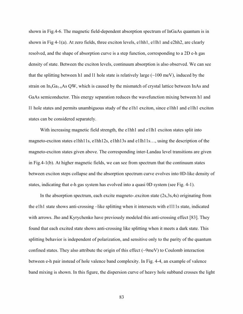
83
shown in Fig.4-6. The magnetic field-dependent absorption spectrum of InGaAs quantum is in
shown in Fig 4-1(a). At zero fields, three exciton levels, e1hh1, e1lh1 and e2hh2, are clearly
resolved, and the shape of absorption curve is a step function, corresponding to a 2D e-h gas
density of state. Between the exciton levels, continuum absorption is also observed. We can see
that the splitting between h1 and l1 hole state is relatively large (~100 meV), induced by the
strain on InxGa1-xAs QW, which is caused by the mismatch of crystal lattice between InAs and
GaAs semiconductor. This energy separation reduces the wavefunction mixing between h1 and
l1 hole states and permits unambiguous study of the e1h1 exciton, since e1hh1 and e1lh1 exciton
states can be considered separately.
With increasing magnetic field strength, the e1hh1 and e1lh1 exciton states split into
magneto-exciton states e1hh11s, e1hh12s, e1hh13s and e1lh11s…, using the description of the
magneto-exciton states given above. The corresponding inter-Landau level transitions are given
in Fig.4-1(b). At higher magnetic fields, we can see from spectrum that the continuum states
between exciton steps collapse and the absorption spectrum curve evolves into 0D-like density of
states, indicating that e-h gas system has evolved into a quasi 0D system (see Fig. 4-1).
In the absorption spectrum, each excite magneto-.exciton state (2s,3s,4s) originating from
the e1h1 state shows anti-crossing –like splitting when it intersects with e1l11s state, indicated
with arrows. Jho and Kyrychenko have previously modeled this anti-crossing effect [83]. They
found that each excited state shows anti-crossing like splitting when it meets a dark state. This
splitting behavior is independent of polarization, and sensitive only to the parity of the quantum
confined states. They also attribute the origin of this effect (~9meV) to Coulomb interaction
between e-h pair instead of hole valence band complexity. In Fig. 4-4, an example of valence
band mixing is shown. In this figure, the dispersion curve of heavy hole subband crosses the light

84
hole subband at certain k value, which causes the wavefunctions of heavy hole and light hole get
mixed also.
4.4.2 PL Spectrum Excited with High Peak Power Ultrafast Laser in High Magnetic Field
We now contrast the above spectrum with PL observed using ultrafast laser pulses. Fig. 4-
7 shows magnetic field dependent PL spectrum from InxGa1-xAs QW excited with 775 nm, 150
fs laser pulses of 10 GW/cm2, which generates carrier density ~1012cm-2. At zero field, we
observe e1h1 and e2h2 interband transitions, and with the increasing of magnetic field these two
PL peaks split into inter-LL transitions (‘Landau fan’). We observed PL from well defined inter-
LL transitions up to e1h15s, but the anti-crossing-like splitting between e1h1ns and e1l1ns in the
absorption spectrum are not observed in this PL spectrum. As mentioned above, the anti-crossing
effect is due to the Coulomb interaction between electrons and holes, therefore, the absent of
mixing of LL states indicated that the Coulomb interaction is screened at high e-h density so that
the corresponding transitions between LL states in Fig.4-7 are not purely excitonic.
For comparison, we plot the Landau fan diagram comparing the absorption spectrum and
PL spectrum under high power excitation in Fig. 4-8. The Landau fan diagram of PL is very
different from the Landau fan diagram of absorption even at high magnetic field. First, for the
same inter-LL transition, the energy position of each PL peak has red shift with that of the CW
absorption peak, which we attribute to carrier density-induced bandgap renormalization [93].
This band gap renormalization is caused by the many body effect of carriers and this many-body
effect gets stronger at high carrier density. Second, at high magnetic field, since the excitonic
effect can be neglected, we have the following form for the energies:
)1(*
++= ncm
eBEE gh , 4-2

85
where E is the energy position of peak of a LL at given magnetic field B, Eg is the band gap, m*
is e-h pair effective mass and n indicates the nth LL. We can see that in equation 4-2, E is
linearly proportional to B and 1/m* is the slope, fitting result shows m*=0.0672m0, m0 is the
electron effective mass. From Fig.4-8, we can see that for a trace of given LL, the effective mass
in the absorption spectrum should be higher than that in the PL line, which indicates that the m*
is higher at low carrier density. Third, in the case of free e-h pairs with no excitonic coupling,
such as in e-h plasma, the traces of all the LLs originate from same subband should converge at
zero field since the Coulomb interaction bind e and h is screened. This effect is consistent with
the traces of LLs in PL spectrum. However, in absorption spectrum, the line of LLs peak
positions do not converge at zero field because of the existing of e-h binding energy. Thus, the
magneto-PL of InxGa1-xAs/GaAs QWs excited with high power ultrafast laser pulses is most
likely plasmonic instead of excitonic.
In Fig.4-9, we plot the magneto-PL excited with different excitation intensity for three
wavelengths (a) 1300 nm, (b) 1100 nm and (c) 775 nm at 25 T. For each wavelength, we denote
the lowest and highest excitation intensity in GW/cm2. The peak position are assigned from
lower energy side 0-0 to higher energy side 1-1, 2-2 and respectively. From the Fig.4-9, we can
see that the excitation with 1.1 μm and 1.3 μm are below InGaAs QW bandgap so that the PL
originates from carriers excited via two-photon absorption into the GaAs barrier and capping
layer as well as the continuum states of InxGa1-xAs QW. For 775 nm as well as 1.1 and 1.3 μm
excitation, PL emission occurs after excited carriers relax down to the QW subbands. In Fig. 4-9,
the peak energies of each LL remain at fixed positions and do not show any red shift at high
pumping intensity. This indicates that the many particle interaction effect is not resolved and the
bandgap renormalization effect is suppressed at low excitation power.

86
In Fig4-9 (a), (b) and (c), we can see that the character of energy peaks 1-1 and 2-2 are
very different from 0-0 peak. At low excitation powers, broad and weak peaks from 1-1 and 2-2
are seen in (b) and (c). With increasing the excitation laser intensity, a narrow peak starts to
appear on the high-energy side of 1-1 and 2-2 peaks and become dominant at high excitation
power. The linewidth of narrow peak of 1-1 is 2.3 meV, smaller than that of 0-0 peak (9 meV),
implying a different emission origin for these two peaks. In addition, we do not observe these
narrow peaks in the magneto-exciton absorption spectrum shown in Fig.4-1.
We plot the 775 nm, 1.1 μm and 1.3 μm laser excitation power dependence of PL intensity
for 0-0 transitions, 1-1 transition, including broad and narrow peaks, in Fig4-9 (d) to (f). For
775nm excitation, the PL intensity from all the three states rise up rapidly at low power
(<2GW/cm2) and then saturates. At 1.1 μm and 1.3 μm excitations, the PL intensity from 0-0
transition and tail of 1-1 transition increases proportionally to I2pump, since the excitation requires
a two photon absorption which scales as the square of laser intensity. However, the narrow peak
of 1-1 transition shows very different scaling. In Fig.4-9 (d), the narrow peak of 1-1 LL transition
shows no emission until threshold pump intensity (~13 GW/cm2), which might be an evidence of
stimulated emission processes.
To understand the many particle effect in the high density of electron hole gas generated
with femtosecond lasers, we plot the magnetic field dependent spontaneous emission calculated
with an 8 band in Pidgeon-Brown effective mass model [94](for details, see appendix B) in
Fig.4-10 (a). Fig. 4-10(b) is the correspondent experimental results. By comparing the two
curves, we estimate that the actual carrier density is between 1012/cm2 and 1013/cm2 in our
experiments. However, there are several discrepancies between theoretical calculation and our
experimental results.

87
(I) The energy peaks of higher LL levels are shifted due to the single particle theory, in which the
Coulomb interactions between electron hole and renormalization effects are neglected.
(II). Spin induced splitting in magnetic field is not observed experimentally due to the large
inhomogeneous broadening of the PL peaks.
(III) The theory does not predict the emergence and power scaling of the narrow emission peaks
at 1-1 LL transition,
We suggest that the experimental curves are induced by new emission processes at higher
lying LLs. More systematic studies are presented in the next chapter to elucidate the origin of
these phenomena.
4.5 Summary
With the underlying theory of LL physics, we have elucidated the conduction and valence
band structure of InxGa1-xAs/GaAs QW. The anticrossing behavior between LLs originate from
different subbands has been discussed. Previous investigation shows that the anticrossing is due
to Coulomb interaction between e-h excitonic pair. Furthermore, by comparing the CW
experimental magneto-absorption spectrum and magneto-PL spectrum with ultrafast high power
laser excitation, it is found that the interaction between e-h is plasmonic rather than excitonic.
Also new sharp features emerge in the PL spectrum of interband LL transitions, which implies
new optical process in the PL emission. That is the subject of Chapter 5.
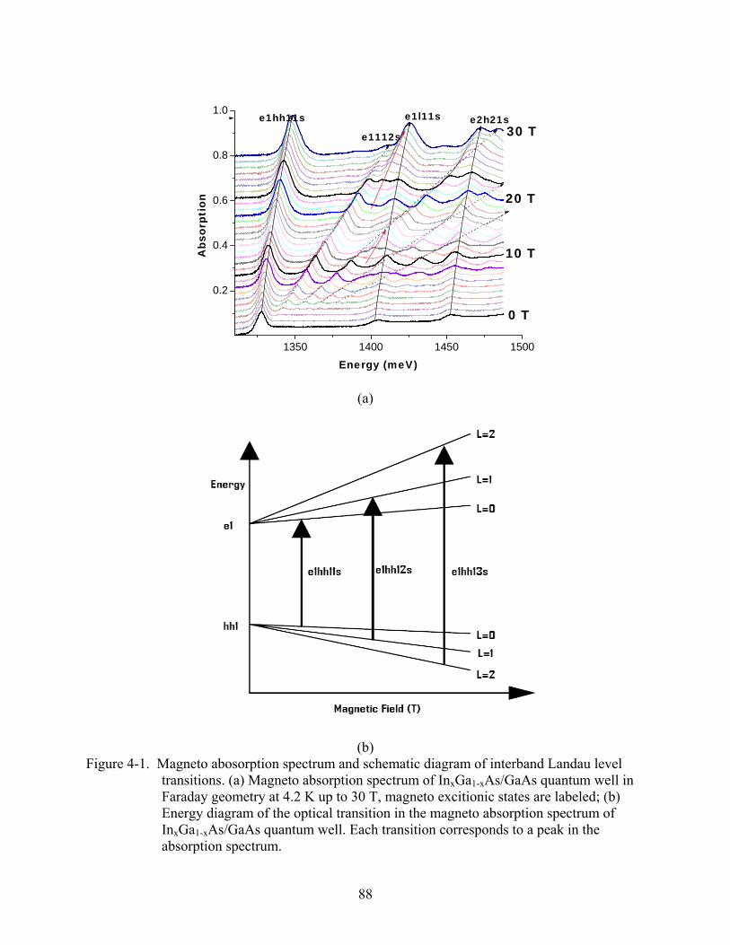
88
1350 1400 1450 1500
0.2
0.4
0.6
0.8
1.0e2h21s
e1112s
e1hh11s e1l11s
0 T
10 T
20 T
30 T
Abs
orpt
ion
Energy (meV)
(a)
(b) Figure 4-1. Magneto abosorption spectrum and schematic diagram of interband Landau level
transitions. (a) Magneto absorption spectrum of InxGa1-xAs/GaAs quantum well in Faraday geometry at 4.2 K up to 30 T, magneto excitionic states are labeled; (b) Energy diagram of the optical transition in the magneto absorption spectrum of InxGa1-xAs/GaAs quantum well. Each transition corresponds to a peak in the absorption spectrum.
89
(a)
(b) Figure 4-2. Magnetophotoluminescence experimental results of band gap change and effective
mass change. (a) Band gap renormalized at high carrier density, (b) Reduced effective mass renormalized at high carrier density in InxGa1-xAs semiconductor QW.Reprint with permission from L. Butov et al., Phys. Rev. B 46, 15156 - 15162 (1992), Figure 2 on page 15158 and Figure 8 on page 15161
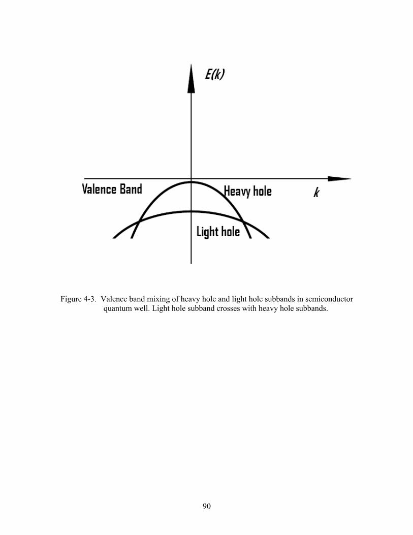
90
Figure 4-3. Valence band mixing of heavy hole and light hole subbands in semiconductor
quantum well. Light hole subband crosses with heavy hole subbands.

91
GaAs Cap layer15nm GaAs
15nm GaAs8nm InGaAs
Buffer
GaAs Substrate
15 Periods
Figure 4-4. Structure of In0.2Ga0.8As/GaAs multiple quantum well used in our experiments.
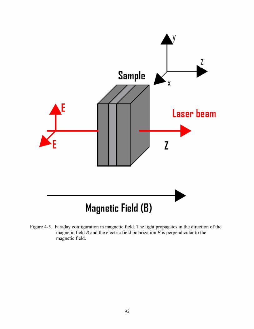
92
Figure 4-5. Faraday configuration in magnetic field. The light propagates in the direction of the
magnetic field B and the electric field polarization E is perpendicular to the magnetic field.

93
Figure 4-6. Energy levels of electron and hole quantum confinement states in InxGa1-xAs
quantum wells. e1,e2, hh1, hh2 denote the electron and hole states due to quantum confinement.
1325meV
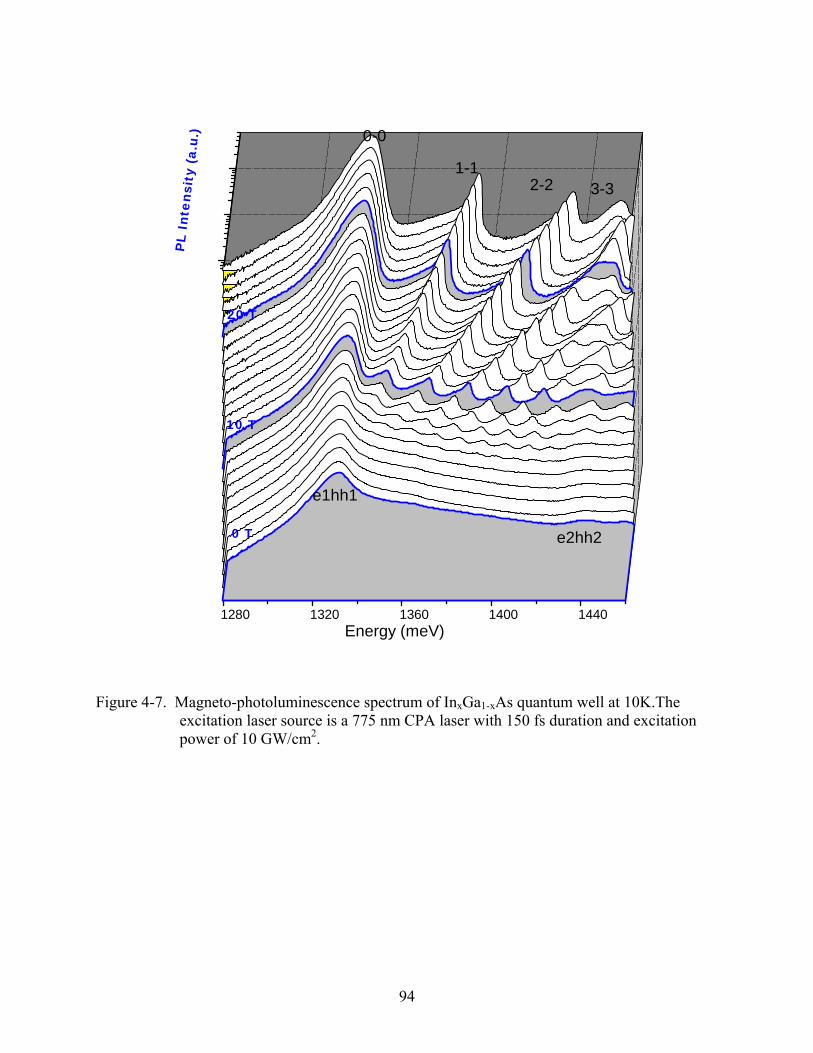
94
1280 1320 1360 1400 1440
e2hh2
3-32-21-1
0-0
e1hh1
10 T
20 T
PL
Inte
nsit
y (a
.u.)
Energy (meV)
0 T
Figure 4-7. Magneto-photoluminescence spectrum of InxGa1-xAs quantum well at 10K.The
excitation laser source is a 775 nm CPA laser with 150 fs duration and excitation power of 10 GW/cm2.
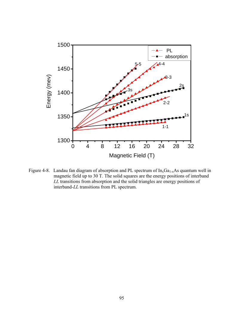
95
0 4 8 12 16 20 24 28 321300
1350
1400
1450
1500
5-5 4-4
3s
3-3
2s
2-2
1s
1-1
PL absorption
Ene
rgy
(mev
)
Magnetic Field (T)
Figure 4-8. Landau fan diagram of absorption and PL spectrum of InxGa1-xAs quantum well in
magnetic field up to 30 T. The solid squares are the energy positions of interband LL transitions from absorption and the solid triangles are energy positions of interband-LL transitions from PL spectrum.
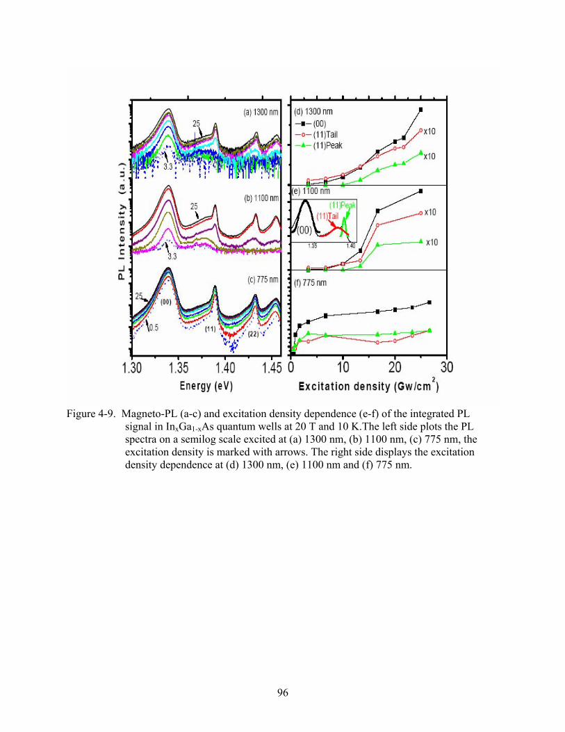
96
Figure 4-9. Magneto-PL (a-c) and excitation density dependence (e-f) of the integrated PL
signal in InxGa1-xAs quantum wells at 20 T and 10 K.The left side plots the PL spectra on a semilog scale excited at (a) 1300 nm, (b) 1100 nm, (c) 775 nm, the excitation density is marked with arrows. The right side displays the excitation density dependence at (d) 1300 nm, (e) 1100 nm and (f) 775 nm.

97
1300 1320 1340 1360 1380 1400 1420 1440 1460 1480
0.01
0.1
(33)
(22)
(11)(00)
(22)(11)(00)
HH2
Experiment
PL (a
rb u
nits
)
Energy (meV)
1E-3
0.01
0.1
1
25 GW/cm2 @ 1.1 μm
PL S
igna
l (nm
-3) Theory npair = 1x1013 cm-2
B = 25 Tesla T = 4.2 K
e1h2
Figure 4-10. Theoretical calculation and experimental results of PL in high magnetic field.
Theoretical calculation of the PL spectrum based on an 8 band Pigeon Brown model (top panel, from Gary Sanders) and experimental results (lower panel) of magneto-PL emitted from InxGa1-xAs with high excitation density at 25Tesla and 4.2K.
98
CHAPTER 5 INVESTIGATIONS OF COOPERATIVE EMISSION FROM HIGH-DENSITY ELECTRON-
HOLE PLASMA IN HIGH MAGNETIC FIELDS
5.1 Introduction to Superfluorescence (SF)
In this chapter, we consider the unique nature of cooperative electro-magnetic emission
made possible using ultrafast laser excitation of quantum wells placed in high magnetic fields.
This combination allows us to create atomic-like behavior between electrons and holes at carrier
densities well above those which support excitons. As such, these ‘simulated atoms’ can emit
light cooperatively via superfluorescence.
The nature of the emission of light from atoms and atom-like systems depends sensitively
on the physical environment surrounding them, and can be tailored by controlling that
environment [96-98]. At the most fundamental level, atom-photon interactions can be modified
by manipulation the number density, phase, and energies of atoms and photons involved in the
interaction. A very common example is the laser, in which mirrors are used to provide coherent
optical feedback to a population inverted atomic system, resulting in the emission of photons
with well-defined spatial and spectral coherence properties. Less common but equally
fundamental examples are the “superemission” processes, superradiance (SR) and
superfluorescence (SF), cooperative spontaneous emission from a system of N inverted two-level
dipoles in a coherent superposition state.
Experiments probing these phenomena in atomic systems have provided significant insight
into the fundamental physics of light-matter interactions [99]. In our experiments, by
manipulating the coherent interactions of electrons and holes in a semiconductor quantum well
using intense ultrashort laser pulses and strong magnetic fields, we generate superfluorescence in
a completely new and unexplored regime. Our experiments begin to approach the question of
whether atom-photon interactions in semiconductors are truly “quantum” as they are in atoms.
99
5.1.2 Spontaneous Emission and Amplified Spontaneous Emission
The simple illustration of spontaneous emission process is shown in Fig.5-1 (a). For a two
level atom system with a high energy excited state E2 and a low energy ground state E1, the
atoms populating the E2 state might spontaneously transit to E1 state without any external
electromagnetic field perturbation. A photon is emitted with energy 12 EE −=ωh , where ω is the
angular frequency of an emitted photon. We can describe this spontaneous emission as [120]
NAdtdN
21−= , 5-1
in which N is the number of atom on excite states E2 and A21 is called spontaneous emission
probability or Einstein A coefficient. The solution of this equation is an exponential decay
function given by
N N et
=−
021τ , 5-2
where N0 is the initial number of atom on E2 state and τ21 is the life time of this transition.
Comparing Eq. 5-1 with 5-2, we haveτ 211
21= −A .
As we know, if atoms are far enough from each other and the interactions between atoms
are neglected, the spontaneous emission that occurs in one atom on excited state is also isolated
from the spontaneous emission from another atom on excited state. Therefore, spontaneous
emission has random directionality. Also as we see from equation 5-1, the intensity of
spontaneous emission is proportional to N, the total number of atoms involved in the transition.
The instinct properties of the atomic system determine the value ofτ 21 , which ranges from μs for
rarified gases to ns for semiconductors. [100-102]
Fig.5-1(b) shows the transition process of amplified emission. In a two-level atom system
as described above, an atom populates the excited state E2. Before this atom relaxes down to the

100
ground state E1 through spontaneous emission, it can be perturbed by the electro-magnetic field
of an incident photon, which is emitted from spontaneous emission with energy h E Eν = −2 1 .
Under the perturbation, this atom might transit to ground state E1, emitting a photon with
energy h E Eν = −2 1 . This photon emission process is called amplified spontaneous emission
(ASE). After this transition, one photon hν is turned into two photons.
ASE process can be described with the following equation [121]
NBdtdN )(21 νρ−= , 5-3
where B21 is a stimulated emission probability, called Einstein B coefficient and ρ(ν) is the
distribution function of radiation density of photons at frequency ν.
The relationship between A21 and B21 is given by [121]
AB c
21
21
3
2 2=hωπ
. 5-4
One important optical property of ASE is that the emitted photon is exactly same as the
incident photon [121]. These two photons have the same optical frequency, spatial phase, optical
polarization, and direction of propagation, which results in the coherence between them.
Through ASE process, weak spontaneous emission can be amplified coherently in active
medium.
However, ASE can occur for any photon created from spontaneous emission, and in a
medium with a sufficiently large density of excited states, many spontaneously emitted photons
can be exponentially amplified in different regions, such that light from different spatial regions
are incoherent since they have different phases, polarizations and propagation directions. If an
optical cavity is used to select a specific mode of ASE, a lasing effect can be observed since all
other ASE processes are suppressed except the preferentially selected ASE mode.
101
In ASE process, in the low intensity regime, where I z I s( ) << , the amplification of emission
intensity in the propagation direction z is written as
I z I eg z( ) ( )= 0 0 , 5-5
in the high intensity saturated gain regime, where I z I s( ) >> , the emission intensity is described
by
I z I I g zs( ) ( )= +0 0 . 5-6
In equations 5-5 and 5-6, I( )0 is the intensity of light propagating in the medium at z=0, Is is the
saturation intensity (which depends on the medium and density of excited states), z is the light
propagation direction, and g N0 2 21≈ σ is called optical gain, where σ 21 is a probability factor
called the stimulated-emission cross-section and usually very small~10-20cm-2 [96].
From the two equations 5-5 and 5-6, we can see that in low intensity regime, the light
intensity grows as an exponentially along the z direction; in high intensity regime, the intensity
grows linearly along the z direction. The gain is said to saturate in high-intensity regime.
5.1.3 Coherent Emission Process--Superradiance or Superfluorescence
In SE or ASE processes, the separation between two atoms on excite states are relatively
large, so that the electro-magnetic field induced by one atom does not interact with the other
atom, and the electric dipole of each transition is not aligned nor has the same phase in the
oscillation, which results in incoherence between different SE processes or ASE originating from
different spontaneous emission processes, also resulting in incoherent emission.
However, in a N-atom ensemble, if the atoms in excited states are brought closer and
closer, so that the electro-magnetic field radiated interact with many excited atoms (in
macroscopic scale) simultaneously and all the atomic electro dipoles oscillate in phase before
they start uncorrelated spontaneous emission, a coherent macroscopic dipole state can exist for a
102
short time. A very short burst of emission will occur, radiating strong coherent light. This
‘superemission’ process is called superradiance (SR) or superfluorescence (SF), depending on
the nature of the initial formation of the macroscopic coherence. For SR, the coherence of atoms
is from the external excitation source, i.e. polarized laser pulse, and excited atoms preserve the
coherence before they emit photons. For SF, the atoms on excited state are initially incoherent,
the coherence develop in the N atoms due to the interaction between them.
The SF emission is a macroscopic coherent effect in an ensemble of N atoms, in which all
the N atoms radiate photons cooperatively and coherently. Fig.5-2 shows the processes of SF
emission. Initially, an ensemble of N atoms populates the ground state. With photoexcitation
from a laser pulse, the N atoms are excited and populate higher energy states. The N atoms
preserve the coherence from the coherent laser pulses for a very short time and then lose the
coherence before they start to transit to ground state. In this situation, the electro dipoles of N
atoms are not aligned in phase. However, if the density is high enough, the electro dipoles could
develop the coherence and get aligned and start to oscillate in phase spontaneously due to the
interaction between them. A small number of electro dipoles of the N atoms could be aligned in
phase spontaneously due to quantum fluctuation or thermal effect, and then this coherence of
electro dipoles is developed to all the atoms through a very high gain mode (α·L>>1). The N
atoms in the coherent state will emit coherent photons in a very short burst of pulse.
SR was first predicted theoretically by Dicke in 1954 [35] and first observed
experimentally by Skribanovitz et al. [103] in hydrogen fluoride (HF) gas in 1973. Many
experiments about SR and SF have been performed and reported in atom gas system [104-106].
In addition to experiments of SF, more theoretical work elucidating the nature of SF under
103
different conditions has also been done with either quantum field theory [107] or semiclassical
theory [108].
In Dicke’s SR theory, the cooperative emission of electro dipoles takes place under the
following condition,
3~ λV . 5-7
Where V is the volume that excited atoms are confined and λ is the emission light wavelength.
From this condition, cooperative emission exists in a very small active medium volume.
However, Bonifacio et al. [107] and MacGillivrary and Feld [108] extended the SF theory
to optically thick medium (on the order of mm or cm), either a “pencil shape” geometry, in
which the Fresnel number (A/Lλ, where A is the cross section and L is the length of active
medium) is not larger than 1 or a “disk shape”, in which Fresnel number is much larger than 1.
In the description of SF, there are five time scales are involved: the “dephasing” times T2
and T2*, the photon decay time τE, cooperative time τc and SF radiation time (or duration) τR, and
coherent delay time τd. τE is the time of a photon transit time in the active medium, T2 and T2* are
the coherence relaxation time due to homogeneous and inhomogeneous broadening effect, τc is
the characteristic exchange time of electro dipole coupled to radiation field, τR is the pulse
duration of SF emission, and τd is the delay time, during which the spontaneous emission evolves
into coherent emission.
The expressions of these time scales τc, τR and τd are given by [108]
2
212
0001
0
2tan
)2ln(16
)2(,)(
)/8(
NTckggNg
LNAT
Rd
kc
eoussponR
πτ
μτ
λπτ
≈
===
=
− h , 5-8
104
where Tsp is the spontaneous radiation time of an atom transits from high energy state to the
lower energy state, N is the number density of atomic system, λ is the transition wavelength, gk0
is the coupling factor between electromagnetic field and electric dipole, which is a key factor in
the evolution of coherent emission, k0 is wave vector of central frequency of optical transition
and μ is the dipole moment of atomic dipole. Another critical factor in the cooperative coherent
emission is the cooperative length Lc, within which all the dipole oscillates in phase, resulting in
the coherent emission. The expression of Lc is given by [108]
ρ02/ gcLc = , 5-9
where ρ is the density of atoms.
In Bonifacio’s theory, the condition for cooperative emission of N atoms ensemble is given
by [108]
*22 ,TTdRc <<<<< τττ . 5-10
Under this condition, initiated by quantum fluctuations or thermal radiation, a small
number of atomic dipoles oscillates in phase and emit photons spontaneously, then through the
coupling between atomic dipoles and electromagnetic field, the N atom oscillators ensemble
develop into oscillatory phase matching state in delay time τd and radiate a short burst of
coherent emission with pulse width τR. Eq. 5-10 stresses that the emission takes place before the
N atoms oscillator become dephased at time T2, T2* and the N atom oscillators develop into
coherent state before they start to recombine.
Bonifacio also mentioned in his theory that the relationship between active medium length
L and critical cooperative length Lc

105
In the case L<<Lc or τE< τc, photons leak out of the active medium before they interact
with the atoms, the N atomic oscillators emit a pure SF, the intensity of pure SF is given below
[108]
))(1(sec)1exp(2
)( 2*
2
220
dR
thTkV
NgtI τ
τ−−= . 5-11
We can see that the peak intensity of SF is proportional to N2 and emission peak is at t=τd.
In the case L<Lc, where τE> τc the photons travel inside the active medium when the SF
emission takes place, SF is still observable, however the emission pattern is oscillatory pattern in
stead of sech2 pattern [108].
In the case L>Lc, the SF emission starts to get weaker and disappear, the emission process
is dominated by ASE [108].
As shown in Eq.5-10, several requirements and characteristics for a system need to be
satisfied to make SF emission observable. SF pulse duration rτ and delay time between
excitation and SF burst dτ are much shorter than the spontaneous emission time eoussponT tan and
inhomogeneous dephasing time ∗T ( ∗<< TT eousspondr ,, tanττ ) so that the electric dipoles can
maintain their phase relation and emit coherent light before spontaneous emission occurs. Based
on these requirements, rarified gas atom systems are the most favorable to observe SF emission,
since they have relatively long eoussponT tan and (~ μs), and the SF pulse width and delay time is on
the order of nanoseconds. Table 5-1 shows some of the time constant in the SF experiment done
in Rb gas. By controlling the pressure of the atomic gas, SF emission pattern can be clearly
resolved [109, 110]. However, in a solid-state system, i.e. semiconductors, the dephasing time
T2, T2* are extremely small (~1ps) [111], and the conditions in 5-10 are very difficult to satisfy.
Thus, up until this work, it has been impossible to observe SF emission in semiconductors.
106
5.1.4 Theory of Coherent Emission Process--SR or SF in Dielectric Medium
In 1964, A. P. Kazantsev [112] reported the first theoretical results of collective emission
processes in a two level system of a dielectric medium, such as a semiconductor. He found that if
the electromagnetic field interacts with two level systems resonantly, the field amplitude is
modulated with a characteristic frequency Ώ, which is the coupling between electric field and
two level systems. The two prerequisites in Kazantsev’s theory can expressed as
10
2
≤=ω
γhNE , 5-12
1≥Ωτ , 5-13
where τ is the relaxation time of two level system, 0ωhN is the energy stored in N atom system.
Also, three simplifications of the two level system in Kazantsev’s theory are made, (1) the
dielectric medium is infinite and sufficiently rarefied, in which case the Ώ<<ω0 , (2) the medium
is a two level system and (3) there is no dissipation in the two level system so that 1/τ~0, only the
early time (t<< τ) is considered.
With the conditions shown above, the intensity of radiation is given by
E t E t( ) ~ exp( )20
2 Ω
022 ~ ωNdΩ , 5-14
where E0 is the initial value of electric field, d is dipole momentum, N is the density of activated
atoms and ω0 is the transition frequency. It can be seen that the intensity of field increases
exponentially and dramatically if the collective modulation frequency Ώ is large enough.
Zheleznyakov and Kocharovsky [113] applied the idea of cooperative frequency, which
couples the electric magnetic field and optical polarization P in the medium, to the coherent
107
process of polarization wave function in dielectric medium, and the cooperative frequency is
given by
( )ω π ωc d N= 8 320Δ / h , 5-15
Where ΔN=N2-N1, which represents the maximum population inversion density in the two
level system.
Belyanin et al. [114-118] calculated the Maxwell-Bloch equations for resonant interactions
between active medium and radiation field in semiconductors. In the mean field approximation,
the slowly varying electromagnetic field E(k), macroscopic polarization wave Pk, and inversion
density ΔNk can be described via a coupled set of equations:
d Edt T
dEdt
E PE
k
2
2 021 4+ + = −ω π , 5-16a
d Pdt T
dPdt
P EK kk
c2
2 02
2242
+ + = −ω ωπ
, 5-16b
d Ndt
N NT
E dPdt
k k kp
kΔ Δ Δ+
−= ∗( )
1 0
2hω
. 5-16c
Here, E is the electric field and Pk is the optical polarization oscillating at frequencyω0 . The
subscript k refers to electron-hole pair with quasi-momentum k, TE is the photon life time for a
given field mode, T1 is the relaxation time of excited state, T2 is the dephasing time of dipoles, d
is the transition dipole moment, n is the refractive index, and ΔN kp is the inversion density
excited by pumping.
From these three equations, we can see that E and P are coupled, with the cooperative
frequency ωc (and thus the density) determining the coupling strength and resulting emission.
The left hand side of 5-16 (a) and (b) for E and P are harmonic oscillators with damping factors
108
TE, T2, and right hand sides are driving force on the oscillators. However, the increasing rate of E
and P strongly depends on the value of ωc, which couples the E and P and dominates the
increasing rate of E and P. The driving force ωc on RHS of 5-16 (b) should be associated with
excited atom density and electric dipoles, and transition frequency in the E and P resonant
interaction, as shown in Eq.5-15. If an initial value of ωc is sufficiently large, equation 5-16
exhibit instability with respect to the growth of small initial oscillations of the E and P.
Given that
ωc
ET21
> , 5-17
equations 5-16 can be solved approximately in two regime [111].
First is amplified spontaneous emission regime. In this case, we have
ωc
T21
2
<< , 5-18
and the growth rate is given by
ω ω"= −c
E
TT41
2 . 5-19
In order to get amplified, then we should have ω ω"= −c
E
TT41
2 >0.
Second is SF regime. In this case, we have
ωc
T21
2
>> , 5-20
and the maximum growth rate of emission intensity is given by
ω ω"≈ c
2. 5-21
109
The SF pulse width τR and coherent length Lc can be estimated with the value of ωc, also
the delay time τD, which characterize the coherent generation can be given as [111]
τω
ω
τω
R
c
D
L cn
Log factor
E E
~"
"( )
~"
log( / )max min
2
10 20
12
≈ × − . 5-22
From the cooperative frequencyωc , many parameters can be derived. The SF pulse
duration scales as
τωSF
c
N~ ~1 12
−, 5-23
and the peak intensity of SF scales as
I N NSFSF
~ ~hωτ
32 . 5-24
The line width of cooperative recombination, which is determined by the band filling of
particle states in QW or QD scales as
21
~~ Ncωω ΔΔ . 5-25
5.2 Cooperative Recombination Processes in Semiconductor QWs in High Magnetic Fields
Naturally, in solid-state systems such as semiconductors, it is quite difficult to observe SR
or SF since T2 in solid-state system is very small (on the order of ps). The ensemble of dipole
oscillators formed by electrons and holes cannot build up coherence before they undergo phase
breaking, since the electron and holes are not localized and easily be involved in collisions such
as electron-phonon, electron-electron, and electron-hole collisions. However, Belyanin pointed
out that in quantized semiconductors, such as a semiconductor QW in high magnetic field or QD,

110
the electron and hole are spatially confined. This confinement reduces the collision probability
and can dramatically increase the dephasing time T2. Meanwhile, the density of states of QW and
QD increase dramatically compared to that of a 3D bulk semiconductor (see chapter 3, equation
3-10 and Fig.3-4). This effect implies that instead of populating in the continuum states in a bulk
semiconductor, electrons and holes mainly confine themselves around the quantized energy
levels because the continuum states are depleted in QW and QD structure. In this case, the
number of dipoles formed by electrons and holes increase significantly at QW energies level E1,
E2, which satisfy the high density of “atoms” requirement of SF (see equation 5-20).
In a high magnetic field, the electron-hole pairs in a InxGaAs1-x QW are effectively
confined in a quasi-zero dimensional state, and manifests this 0D effect in the absorption
spectrum and PL spectrum (see Fig. 4-4 and 4-7). The electron-hole pair only populate at
discrete LL states, ensuring that the spreading of the electron-hole pair energies is small, favoring
SF generation. Moreover, the density of state of LL levels for InxGaAs1-x/GaAs QW is high
(~1012/cm2 at 20T, see Chap. 4, equation 4-13), which also give rise to the generation of
cooperative phenomena.
5.2.1 Characteristics of SF Emitted from InGaAs QW in High Magnetic Field.
As mentioned before, semiconductor nanostructures such as QWs or QDs are an ideal
system to observe cooperative recombination of electron-hole pairs, therefore we chose
InxGaAs1-x/GaAs multiple QWs as our emission medium, using ultrafast excitation and high
magnetic field in combination to observe SF. The structure of this sample has been discussed in
4-3 and Fig.4-2.
According to the results shown above (Eqs. 5-17 to 5-21), the key term that determines the
growth rate of emission intensity I, which corresponds to the cooperative emission process is the
cooperative frequency ωc.
111
In a two-dimensional semiconductor quantum well structure, the cooperative frequency is
modified into the following form [114],
ω πλc
QW
d N cn L
=8 2 2
2Δ Γ
h. 5-26
Here LQW is quantum well of thickness, λ is emission wavelength, Γ is the effective overlap
factor of electromagnetic field with the quantum well in the direction perpendicular to well
plane, n is the refractive index and d is the transition dipole. The maximum photo excited
electron-hole density is ΔN ~Ne-h.
Based on the theory presented above, we can estimate the parameters for SF emission in
the InxGaAs1-x/GaAs used in these experiments.
The photon decay time is c
FLnE ~τ ~2x10-13 s-1, where L is the active medium length, F
is the Fresnel number. In reality, 4x10-13 s-1 seems to be a better estimate because the excited
medium can guide the SF emission into the active medium. This waveguide effect is generated
after medium is excited, due to an enhancement in the refractive index medium in the active area
from the magneto-plasma, In this case the electro magnetic field will couple more with optical
polarization.
The cooperative frequency at initial time is given by equation 5-26, where ΔN is carrier
density in the quantum well plane, and Γ is around 1/3. The estimation of cooperative is
21210~ −cm
Ncω ×3×10¹³s-1. In equation 5-20, in order to make the condition for SF satisfied, T2
is ~ 10-13 s-1, and we need N > 5×1011 cm-2, which can be realized at high magnetic field
(~20Tesla) and ultrafast pumping (see chapter 3, equation 3-14).
112
Below, we present investigations of the magneto-PL spectrum obtained from high-density
electron-hole plasmas in InxGaAs1-x /GaAs QW in high magnetic fields, in which propagation of
PL is perpendicular and parallel to the QW plane. Perpendicular to the QW plane, abnormally
sharp and strong emission lines from 0-0 and 1-1 LLs are observed as discussed in chapter 4. As
we have discussed above, there is possibility that this emission is from ASE or macroscopic
cooperative recombination--SF. Since the electron-hole pairs are mainly populating in the QW
plane, the in-plane PL should be much stronger than the PL collected perpendicular to the plane
because the spontaneous emission should be amplified when propagating in the in-plane path.
Thus, we have developed experiments in new configurations to measure the in plane PL from
InxGaAs1-x /GaAs QW.
In order to show definitive evidence of cooperative recombination in QWs in high
magnetic fields, there are a number of experimental signatures that uniquely characterize SF
emission. These are listed in Table 5-2. For comparison, we also include the ASE characteristics
in the Table 5-2, since PL emission in InxGaAs1-x /GaAs QWs at high magnetic fields could be
due to either emission mechanism. From these six characteristics, we can distinguish a pure SF
process from ASE processes, and they are given as follows.
5.2.2 Single Shot Random Directionality of PL Emission
In an SF emission process, the coherent collective emission builds up stochastically from
spontaneous emission, which can be emitted in any direction, and a specific SF burst will follow
the propagation direction that the first spontaneous emission takes. It is essential to note that
since this is a probabilistic quantum electro-dynamic process, each SF burst forms independently
on each subsequent excitation laser pulse. By contrast, in ASE processes many spontaneous
emissions could be amplified, therefore, in a single shot, the PL emission should equally
distribute in all direction and no random directionality is expected.
113
5.2.3 Time Delay between the Excitation Pulse and Emission
As we seen in Eq. 5-21, the SF emission is given after the excitation pulse, the delay time
between is τd, during which the spontaneous emission develops into SF through an extremely
high gain mode. This delay occurs because of the inherent build up time for the coherence form
from the initially incoherent dipole population. In ASE, the emission process start in a short time
(on the order of nl / c < τd, where c is the speed of light and l is the length of activated medium
and n is the refractive index) immediately after the excitation pulse disappears, therefore, no time
τd delay is expected to be observed.
5.2.4 Linewidth Effect with the Carrier Density
In the formation of ASE, spontaneous emission is amplified when travels through medium,
however, the amplified emission linewidth depends on the gain function G(ω), which is given
below,
))(exp()()( 0 LGII ωωω •= . 5-27
Where I0(ω) is the initial intensity function in frequency domain and L is active medium that
light get amplified. Usually, G(ω) has Gaussian or Lorentz shape, which result in the center
frequency in I(ω) get amplified more than frequency off center. This gain narrowing effect
reduces the emission linewidth in ASE process.
In SF process, as mentioned above in Eq. 5-22, the linewidth of cooperative emission is
broadened at high densities, Δω ~ Ne h−1/2, since more carriers are involved in the cooperative
emission.
5.2.5 Emission intensity Effect with Carrier Density
In an ASE process, emission is amplified linearly with N, so that the emission intensity
should increase linearly with the increasing of carrier density N. In an SF process, according to

114
equation 5-23 the emission is a short burst and given coherently, superlinear increasing of the
emission intensity is expected when carrier density N is increased.
In magnetic field, the carrier density N depends on the magnetic field strength B (see
chap.3, equation 3-14), the linear relation between them is N~B, so a superlinear relation, I~B3/2,
between emission intensity and magnetic field is expected in SF emission.
5.2.6 Threshold Behavior
Both ASE and SF exhibit threshold behavior with respect to laser excitation intensity.
However, in ASE, the threshold is at the point where optical gain G>0, while in SF, the
threshold is the point where coherence is built up among carriers.
5.2.7 Exponential Growth of Emission Strength with the Excited Area
Both ASE and SF will be amplified in the form of )exp(~ 0 LII •α , so that the emission
strength increases exponentially with respect to the excited area. Therefore this doesn’t
distinguish between be ASE and SF, but does show that an exponential process is occurring.
We expect to see cooperative emission from high carrier density electro-hole plasma in
InxGaAs1-x /GaAs QW in high magnetic field, however, in order to fully fill the LL and make the
carriers populate on LL before they start to recombine (time scale ~100ps), a high power
(GW/cm2) ultrafast CPA laser is needed to generated enough carrier density in a very short time
(~ps). It is also critical to note that the initial excitation at 800 nm, is well above (240meV) the 0-
0 LL levels that we probe (at 920nm). In fact we excite electrons carrier into GaAs barrier
continuum states and InxGa1-xAs well continuum stats., Most of electrons carriers populating in
barrier are dumped into the InxGa1-xAs QW layer and increase the carrier density in well layers.
Carries in QW layers will relax down to 0-0, 1-1….LL levels and there are many collisions
during the energy relaxation (and momentum relaxation) which completely destroys the initial
115
coherence of carriers imposed by the laser. Thus, we can are truly probing SF as opposed to SR.
After energy relaxation to the QW LLs, the carriers, now tightly confined both in space and
energy, develop into a coherent state with interacting with the electromagnetic field from initial
spontaneous emission and give a burst of SF emission. This process shows the key signature of
SF instead of SR.
5.3 Experiments and Setup
To understand the PL emission processes in InxGaAs1-x/GaAs QWs excited with high
intensity short laser pulses at high magnetic fields, several experiments have been carried out.
• Magnetic field and excitation power dependent in-plane PL
• Single shot experiment for random directionality of in-plane PL
• Control of coherence of the in plane PL from InxGa1-xAs QW in high magnetic field.
In all the experiments, we use the ultrafast magneto-optics facility developed by us at the
NHMFL (see chap2, Figs.2-2, 2-3, and 2-4.). All the experiments are done at liquid helium
temperature with the Janis optical cryostat designed for a resistive magnet. The InxGaAs1-x/GaAs
QW sample is mounted on the liquid He tail of cryostat for direct optics, in which laser beam can
travel in free space and then excite the sample without being chirped.
For most of the experiments, the ultrafast CPA laser system is the excitation light source,
which has been introduced in Chap.4, 4.3. The excitation laser is focused on the InxGa1-xAs QW
sample with one 1 m focal length lens, and the spot size on sample is around 500 μm.
The configuration of the in plane PL collection geometry is shown in Fig. 5-3. In order to
collect the PL travels in the QW planes, a small right angle roof prisms is mounted on the edge
of the QW sample, which can steer the in plane light into the optical multimode fiber mounted
right on the top of the prism. The area of prism is 1.0x1.0mm2, and the fiber diameter is 600 μm.

116
The collection angle for this prism is approximately 40˚. With this configuration, PL emission
travels in the QW plane is effectively and efficiently collected and delivered to a McPherson
spectrometer for analysis. In addition, for comparison with the in-plane PL, PL emission
perpendicular to the QW planes is collected via a fiber on the back face of the sample.
The magnet used for study of cooperative emission is Bitter resistive magnet located in cell
5 at NHMFL, a 25 Tesla (upgraded to 31 Tesla now) wide bore (50 mm) magnet (see Fig.2-1).
Most of our spectra were collected by averaging over multiple shots (1000 shots in most
cases). However, to probe the directionality of the emission, in which the PL propagation is
different from pulse to pulse, single shot experiments need to be performed to resolve this
phenomenon. Thus, we measured the PL from InxGaAs1-x/GaAs QWs excited by one single laser
pulse. An electro-optical Pockel cell was employed in this experiment. As shown in Fig. 5-4, the
laser beam propagates through two crossed polarizers and gets rejected at the second polarizer.
However, there is fast transient high voltage bias nonlinear crystal positioned between the two
polarizers, which operate as a transient half wave plate when the high voltage bias is on. Each
time when the high voltage is on, the high voltage biased crystal changes the polarization of laser
beam by 90 degree and let it go through the second polarizer. With this device, we can control
the number of laser pulses and the repetition rate of the pulses that are sent to the sample and
collect PL from a single excitation pulse.
Also, in order to compare the PL intensity at different in plane directions, two small right
angle prisms are mounted at cleaved edges 90° apart of InGaAs/As QW, which will
simultaneously collect the PL excited with one CPA pulse and steer into two fibers mounted on
top of roof prism. The excitation geometry of single shot measurement is shown in Fig.5-8
117
5.4 Experimental Results and Discussion
5.4.1 Magnetic Field and Power Dependence of PL
We measured the field dependency in plane PL emission spectrum of InxGa1-xAs/GaAs
QW excited with 150fs CPA laser pulses at a constant laser fluence (Flaser~ 0.62 mJ/cm2) up to
25 Tesla. Experimental result is shown in Figure 5-5(a). For comparison, PL collected at the
same conditions with the center fiber is also shown in Fig. 5-5(b). The sharp in the edge
collection PL spectrum is a lot stronger than the PL from center collection. Broad PL emissions
due to spontaneous emission from inter band LL transition are observed up to 12 Tesla. This
broad linewidth (~9 meV) is due to inhomogeneous broadening, which originates from the
inhomogeneities and possibly defects in the multiple QW layers. The magnetic field dependent
PL features above 13 T change dramatically, and sharp peaks (around ~2 meV) are observed on
high energy side of broad feature of each interband LL transition. These sharp peaks dominate
the PL at high magnetic field. However, each inter LL transition PL peak consist of overlapping
broad and sharp peaks, shown in Fig.5-6. The sharp peaks are believed to be ASE or SF and their
linewidth is determined through homogeneous broadening, since the emission concentrates
around a narrow frequency. We fit the field dependent PL strength of 0-0 LL transitions with a
combination of Gaussian function (for inhomogeneous broadening line width) and Lorentz
function (for homogeneous broadening line width) given below.
Gaussian function
20 )exp()(w
AIωω
ω−
= , 5-28
where 1.386 w is the FWHM (full width at half maximum) linewidth, ω0 is the center frequency
of PL transition.
Lorentzian function

118
))(
()( 220 wwBI
+−=
ωωω , 5-29
where w is the FWHM and ω0 is the center frequency of PL transition.
The fitting results of sharp peak emission strength (black dot) and linewidth (red dot) of PL
from 0-0 LL transitions vs. the magnetic field strength are shown in Fig.5-5 (c). In Fig.5-7(a) at a
fixed magnetic field of 20 T, the PL spectrum of interband LL transition vs. excitation laser
fluence is plotted. It is observed that below certain laser fluence (0.01 mJ/cm-2), only broad PL
peaks with linewidth (~9 meV) exist, but with the increasing of laser Fluence, a sharp peak starts
to emerge on the high energy side of broad peak. At the highest excitation laser fluences, the
sharp peak dominates the PL emission spectrum. With the same fitting procedure as used for the
magnetic field dependent PL spectrum, laser fluence dependent emission strength and linewidth
of sharp PL peak from interband 0-0 LL transition are obtained and shown in Fig 5-7(b).
Identical field and laser fluence dependent PL spectra are seen when collecting from the
center fiber above the pump spot, i.e., out of plane, although at a much lower signal level
(~1/1000). Also, increasing or decreasing the pump spot size resulted in the emergence of sharp
PL features in the spectra at a given fluence. Thus, the observed behavior is not due to a spatially
or spectrally inhomogeneous distribution of carriers.
Comparing the fitting results in Fig. 5-5(b) and 5-7(b), we can see similar patterns in
curves of magnetic field or laser fluence dependent emission strength and linewidth. There are a
few regimes in the two set of curves. First, below 12 T (or 0.01 mJ/cm2), narrow emission is not
observed. In the range 12–14 Tesla or (0.01–0.03 mJ/cm2), the narrow peak signal strength S
grows linearly (S~B or Flaser, see green lines)) with respect to both B and Flaser. Second, above 14
T (0.03 mJ/cm2), the emission strength S starts to show a superlinear increase (S ~ B3/2, see blue
lines) with respect to B or Flaser. Above 0.2 mJ/cm2 (see Fig. 5-7(b)), the signal resumes a linear

119
scaling. Also, the field and Flaser dependent PL linewidths curve (red circles) plotted in Figs. 5-
5(b) and 5-7(b) reveal a remarkable correlation with the field and fluence dependent emission
strength curve. In the linear regime, the linewidth decreases monotonically both versus B and
Flaser until the emission becomes superlinear at the threshold point (B=12T and Flaser=0.01mJcm-2
) , where the PL linewidth begins to increase.
At a 20 Tesla, setting the excitation spot diameter at 0.5mm, 0.1mm and 3mm, we also
measured on fluence dependent PL spectrum respectively. The fitting results of emission
strength and linewidth at different excitation spot sizes are plotted inFig.5-8 (b) (c) and (d),
narrow emission was observed, but both the integrated signal S and the linewidth exhibited
qualitatively different scaling for each different spot size. The curve in Fig. 5-8(b) shows the
increasing pattern with increasing laser fluence as shown before (See Chap. 5-4, II) , however,
the emitted signal S in (c) and (d) shows an almost linear relation with respect to the Flaser
(S~Flaser), and in both of (c) and (d), and the linewidth curves monotonically decreased with
increasing fluence.
5.4.2 Single Shot Experiment for Random Directionality of In Plane PL
With a optical Pockel cell, we are able to reduce the repetition rate of CPA laser to very
low frequency (~20Hz) so that we can use the mechanical shutter (speed ~20 ms) on McPherson
spectrometer to record the PL spectrum from a single CPA laser pulse excitation. Also we collect
the in plane PL with two optical fibers simultaneously (the fibers are mounted on QW edges
perpendicular to each other (see Fig. 5-4)), then deliver them to spectrometer to resolve the PL
spectrum propagating in different directions in QW. This measurement is crucial for determining
the correlation of the emission and single shot directionality of the in plane PL emission. Figure
5-4 presents the directionality measurements of the emission for a single pulse excitation. Figure
5-9 (a) illustrates a series of spectra upon single pulse excitation at a given fluence in the

120
superlinear emission regime (Flaser 9.7 mJ/cm2, B=25 T) for a 0.5 mm diameter spot size. The
spectra are collected through fibers on edge 1 (black) and edge 2 (red). We can see that the
relative height between the red and black curve changes from shot to shot, which indicates that
the propagation direction of in plane PL could be different from pulse to pulse since the two
optical fibers are mounted to collect PL propagating in different directions. Since the two optical
fibers have different collection efficiency, in Fig.5-9 (b) we displayed the maximum peak height
from each edge (normalized to 1.0) versus shot number for the pumping conditions shown in Fig.
5-10(a). The maximum observed emission strength in Fig. 5-9(b) fluctuates as much as 8 times
the minimum value, far greater than the pump laser pulse fluctuation (~2%). This strong
anticorrelation between signals received from different edges indicates a collimated but
randomly changing emission direction from pulse to pulse, as expected for cooperative
spontaneous emission.
At a lower excitation fluence in linear increasing regime Flaser ~ 0.02 mJ/cm2 (obtained with
a 3 mm spot), we also measured the shot to shot PL spectra collected with the same configuration
discussed above and show it in Fig 5-10(a). We observed qualitatively different emission
strength behavior from high power excitation shown in 5-10(a). In Fig.5-10(a), the emission
strength of different shot from the same optical fiber do not fluctuate as much as high power
excitation. In Fig.5-10(b) we can see that the normalized (to 1) shot to shot PL emission strength
at different collection direction are highly correlated instead of anti-correlated in high power
excitation. Fig. 5-10(b) shows omnidirectional emission on every shot, as expected for ASE or
SE.
5.4.3 Control of Cherence of In Plane PL from InGaAs QW in High Magnetic Field
As discussed in Chap. 5.3, the intensity of cooperative emission or ASE increases
exponentially with respect to the active length of medium in the propagating direction. We

121
shaped the excitation laser pulse and probed the spatial and directional characteristics of the PL
emission process (see Fig.5-11). Using a cylindrical lens to focus the excitation laser beam on
the QW sample, we generate an elliptically shaped spot (‘pencil geometry’) for the excitation
region. When the cylindrical lens is rotated, we change the active medium length of PL emission
propagating towards the two right angle roof prisms. The emission strength collected from the
prisms should change according to the rotation angle. We define the 0 degree angle at the point
where in plane PL from edge one is at maximum. We measured the signal as a function of angle
from 0 to 180 degree for Flaser ~ 0.02 mJ/cm2 and B~ 25 T (shown in Fig. 5-12), from which we
can see that the PL emission strength change dramatically with respect to the angle cylindrical
lens. In the experiment, the maximum signal from edge one, which correspondent to activated
length 1.5mm is at 90 degree, the minimum signal from edge one is at 0 degree, correspondent to
activated length 0.5mm. The ratio of signal strength 20min
max =II corresponds to 20~)5.0/5.1exp( ,
which is consistent with exponential increasing of emission strength vs. activated medium length
in ASE or SF..
5.4.4 Discussion
With the analysis of all the experimental result shown in Fig. 5-5, 5-7, 5-8 and 5-10, we
found that for the interband 0-0 LL transition, the scaling of the emission strength S, the
linewidth evolution, and single shot emission directionality indicate the following evolution
processes as excitation power Flaser and magnetic field strength B are increased: (i) In the low-
density limit (B<12 T, Flaser < 5μJ/cm2), excited e-h pairs relax and radiate spontaneously
through interband recombination. The emission is isotropic with an inhomogeneous Gaussian
shape linewidth of ~9 meV. This broad spontaneous emission can be seen in both Fig.5-5(a) at
low magnetic field and in Fig. 5-7(a) at low laser fluence. (ii) At a critical fluence 0.01 mJ/cm2

122
(at 20 T) and magnetic field B~12 T (at Flaser ~ 0.6 mJ/cm2), a carrier population inversion is
established with increasing magnetic field and excitation laser fluence, which increases the
carrier density in QW (since N~Flaser and N~B, see equation 3-14). In this case, ASE develops,
leading to the emission of amplified pulses. Fig. 5-10 shows that ASE is simultaneously emitted
in all directions in the plane. The reduction in linewidth with increasing fluence results from
conventional gain narrowing discussed in section 5-2-1, in which spectral components near the
maximum of the gain spectrum are preferentially amplified than components with greater
detuning [see Figs. 5-5(a) below 17 T and Fig.5-7(a) below 0.03mJ/cm2]. In this high-gain
regime, the spectral width reduces to 2 meV (FWHM), still larger than 2/T2. (iii) If we keep
increasing the magnetic field and laser fluence, since the DOS and physical density in QW are
sufficiently high at high magnetic field (at B~20T, N~1012cm-2), the cooperative frequency ωc
exceeds 2/(T2T2*)1/2, the build-up time of coherence between transition dipoles are shorter than
the decoherence time. The e-h pairs establish a macroscopic dipole after a short delay time and
emit an SF pulse through cooperative recombination (or a sequence of pulses, depending on the
pump fluence and the size of the pumped area).
According to the theoretical expression of Δω in cooperative emission regime, the
linewidth of emission increase with increasing of laser fluence due to reduced pulse duration of
cooperative emission, until eventually saturation (due to the filling of all available states) halts
the further decrease in pulse duration (shown in Fig.5-7(b), above 0.2mJcm-2). The transition
from ASE to cooperative emission at 0.03 mJ/cm2 at 20 Tesla is shown in Fig. 5-7(b), we can see
that the linewidth of emission starts to increase significantly, which is consistent with Δω
increasing with increasing of carrier density (predicted in Eq. 5-29).
123
In ASE, the spontaneous emission is amplified during propagation in certain direction.
However, since there are many spontaneous emission photons propagating in different directions
with subsequent amplification, we observe that in a single shot measurement, ASE emission
distribute in all directions. Significantly, we find that unlike ASE, which should be emitted in all
directions with the same intensity [see Fig. 5-10(b)], in this super linear regime the initial
quantum fluctuations grow to a macroscopic level to establish coherence and lead to strong
directional fluctuations from shot to shot [see Fig. 5-9(b)] This is consistent with the random
direction distribution discussed in Chap5, 5.2.1 a. The linear scaling of linewidth vs Flaser above
0.1 mJ/cm2 is a combined result of absorption saturation of the pump and saturation of SF
emission.
As discussed in Chapter 5, the intensity of cooperative emission increasing super linearly
with respect to increasing of carrier density (I~N3/2). Since the carrier density is proportional to
Flaser or B, we should expect observe I~B3/2 or I~F3/2laser in the experiments. However, since the
data was collected in a time-integrated fashion with spectrometer and CCD, we cannot directly
probe the peak SF intensity scaling mentioned before because the SF emission is on the order of
hundreds femtoseconds. However, there are two lines of evidence indicating that the observed
superlinear scaling is related to the formation of multiple SF pulses from the 0-0 LL transition.
The superlinear increase for the 0-0 LL emission is accompanied by an emission decrease from
higher LLs, indicating a fast depletion of the 0-0 level through SF followed by a rapid relaxation
of e-h pairs from higher LLs and subsequent reemission. Also, in the single pulse measurements
shown in Fig. 5-9, data shows that the PL emissions collected from two fibers on different edges
of QW sample are either correlated or anticorrelated in roughly equal proportion. This result
indicates that fast relaxation from higher LLs refills the 0-0 LL, resulting in a second pulse of SF

124
emission in a random direction. On average, the two SF pulses in one excitation pulse are
collected in two different edge takes 50% shots, and for the other 50% shots, the two SF pulse
from one excitation go to the fiber on only one edge. This is in qualitative agreement with
observations, in which 50% shots are correlated and 50% are anticorrelated.
One could argue about weather the observed emission characteristics are consistent with
pure ASE (‘‘lasing’’), but this can be ruled out by examining the excitation power dependent
experiments at 20 T at different excitation spot sizes. In Fig. 5-8(b), (c) and (d) three spot sizes
0.5 mm, 0.1 mm and 5 mm are selected for the experiments. We can see that, only in the S vs.
Flaser curve with excitation with 0.5mm spot size, linear and super linear increasing behavior (the
signature of cooperative emission) emerge. Also a gain region of 0.5 mm is consistent with the
theoretical predication of coherent length )/(~ SESFSFc IILncL τ , which is found to be a few
hundred micrometers. However, in the S~Flaser curve with 5mm excitation spot size, we only
observe linear increasing behavior, this is a typical ASE process, also the linewidth of the PL
emission keeps decreasing with increasing of Flaser,, which is the gain narrowing effect in ASE.
In the curve with excitation spot 0.1mm, we can see that the linewidth decreases up to certain
Flaser,(~0.6mJcm-2), then it stop decreasing. Also we can see that the emission strength S is
neither linearly nor superlinearly increasing with Flaser, increasing. The PL emission with 0.1 mm
excitation spot might be a combination of ASE and SF or early stage in SF. In the case that the
excitation spot size is either much larger or much smaller than the coherent length, and none
optical cooperative emission signature is observed.
We can conclude that collimated, randomly directed emission and superlinear scaling are
observed only when the pumped spot is 0.5 mm, approximately equal to the theoretically
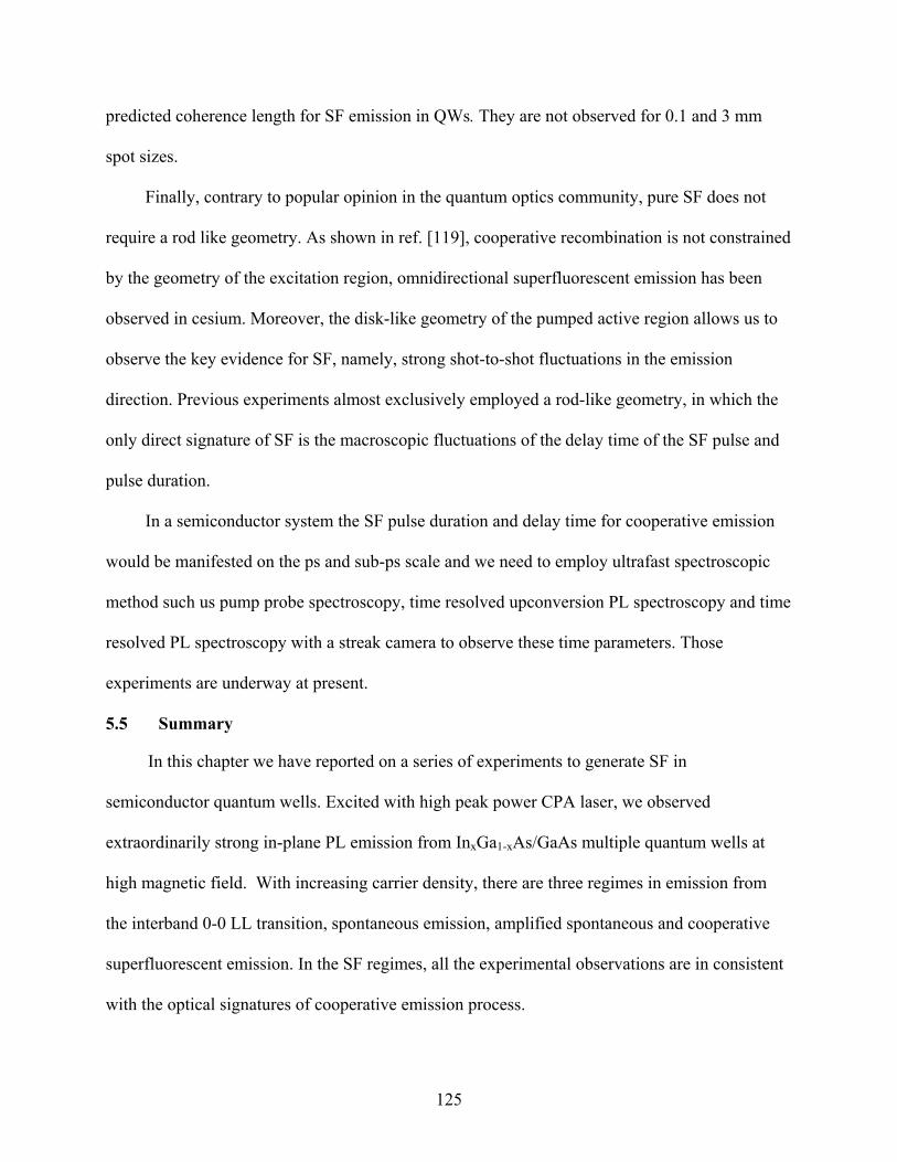
125
predicted coherence length for SF emission in QWs. They are not observed for 0.1 and 3 mm
spot sizes.
Finally, contrary to popular opinion in the quantum optics community, pure SF does not
require a rod like geometry. As shown in ref. [119], cooperative recombination is not constrained
by the geometry of the excitation region, omnidirectional superfluorescent emission has been
observed in cesium. Moreover, the disk-like geometry of the pumped active region allows us to
observe the key evidence for SF, namely, strong shot-to-shot fluctuations in the emission
direction. Previous experiments almost exclusively employed a rod-like geometry, in which the
only direct signature of SF is the macroscopic fluctuations of the delay time of the SF pulse and
pulse duration.
In a semiconductor system the SF pulse duration and delay time for cooperative emission
would be manifested on the ps and sub-ps scale and we need to employ ultrafast spectroscopic
method such us pump probe spectroscopy, time resolved upconversion PL spectroscopy and time
resolved PL spectroscopy with a streak camera to observe these time parameters. Those
experiments are underway at present.
5.5 Summary
In this chapter we have reported on a series of experiments to generate SF in
semiconductor quantum wells. Excited with high peak power CPA laser, we observed
extraordinarily strong in-plane PL emission from InxGa1-xAs/GaAs multiple quantum wells at
high magnetic field. With increasing carrier density, there are three regimes in emission from
the interband 0-0 LL transition, spontaneous emission, amplified spontaneous and cooperative
superfluorescent emission. In the SF regimes, all the experimental observations are in consistent
with the optical signatures of cooperative emission process.

126
Table 5-1. Some experimental conditions for observation of super fluorescence in HF gas. The time unit is nanoseconds, L is the length of activated gas, and d is the size of laser beam.
Active length (cm)
d (μm)
T2* τ E τ R τ D αL
5.0 432 5 0.17 0.15 6-20 353.6 366 32 0.07 0.15 5-35 1802.0 273 5 0.35 0.12 6-25 45
Reprint with permission from M. Gibbs et al., Phys. Rev. Lett. 39 (1977), page 549.

127
Table 5-2. Characteristics of SF emitted from InGaAs QW in high magnetic field Characteristics
Superfluorescence(SF) Amplified Spontaneous Emission(ASE)
Shot to shot random directionality
Yes No
Pulse delayed by τd (~10ps)
Yes No
Emission linewidth increase with carrier density N
Yes No
Emission strength increase with excitation density
Superlinear (~I1.5) Linear (~I)
Threshold behavior Yes Yes Exponential growth with area (~exp(gL))
Yes Yes

128
(a)
(b) Figure 5-1. Spontaneous emission and amplified spontaneous emission process of a two level
atom system.(a) Spontaneous emission (SE); (b) Amplified spontaneous emission (ASE).
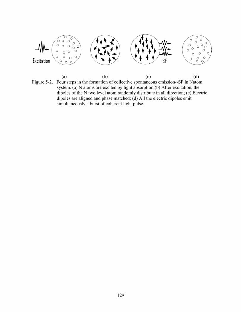
129
(a) (b) (c) (d) Figure 5-2. Four steps in the formation of collective spontaneous emission--SF in Natom
system. (a) N atoms are excited by light absorption;(b) After excitation, the dipoles of the N two level atom randomly distribute in all direction; (c) Electric dipoles are aligned and phase matched; (d) All the electric dipoles emit simultaneously a burst of coherent light pulse.
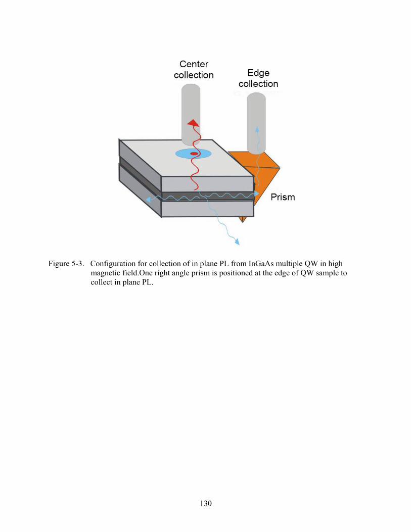
130
Figure 5-3. Configuration for collection of in plane PL from InGaAs multiple QW in high magnetic field.One right angle prism is positioned at the edge of QW sample to collect in plane PL.
131
Figure 5-4. Configuration for a single shot experiment on InxGa1-xAs Multiple QWs.
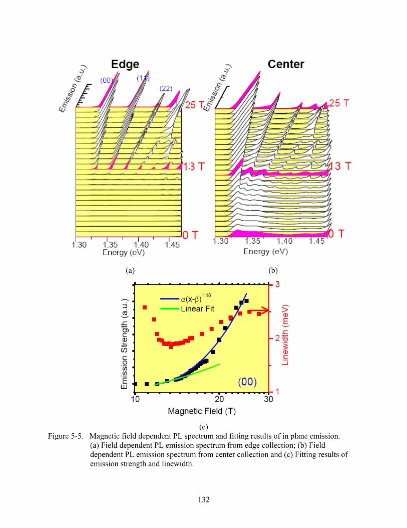
132
(a) (b)
(c)
Figure 5-5. Magnetic field dependent PL spectrum and fitting results of in plane emission. (a) Field dependent PL emission spectrum from edge collection; (b) Field dependent PL emission spectrum from center collection and (c) Fitting results of emission strength and linewidth.
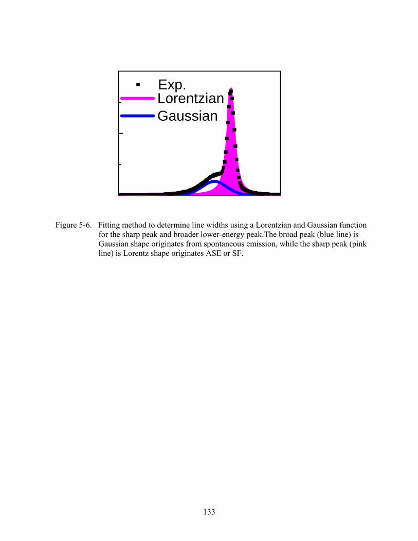
133
Exp.
Lorentzian Gaussian
Figure 5-6. Fitting method to determine line widths using a Lorentzian and Gaussian function
for the sharp peak and broader lower-energy peak.The broad peak (blue line) is Gaussian shape originates from spontaneous emission, while the sharp peak (pink line) is Lorentz shape originates ASE or SF.
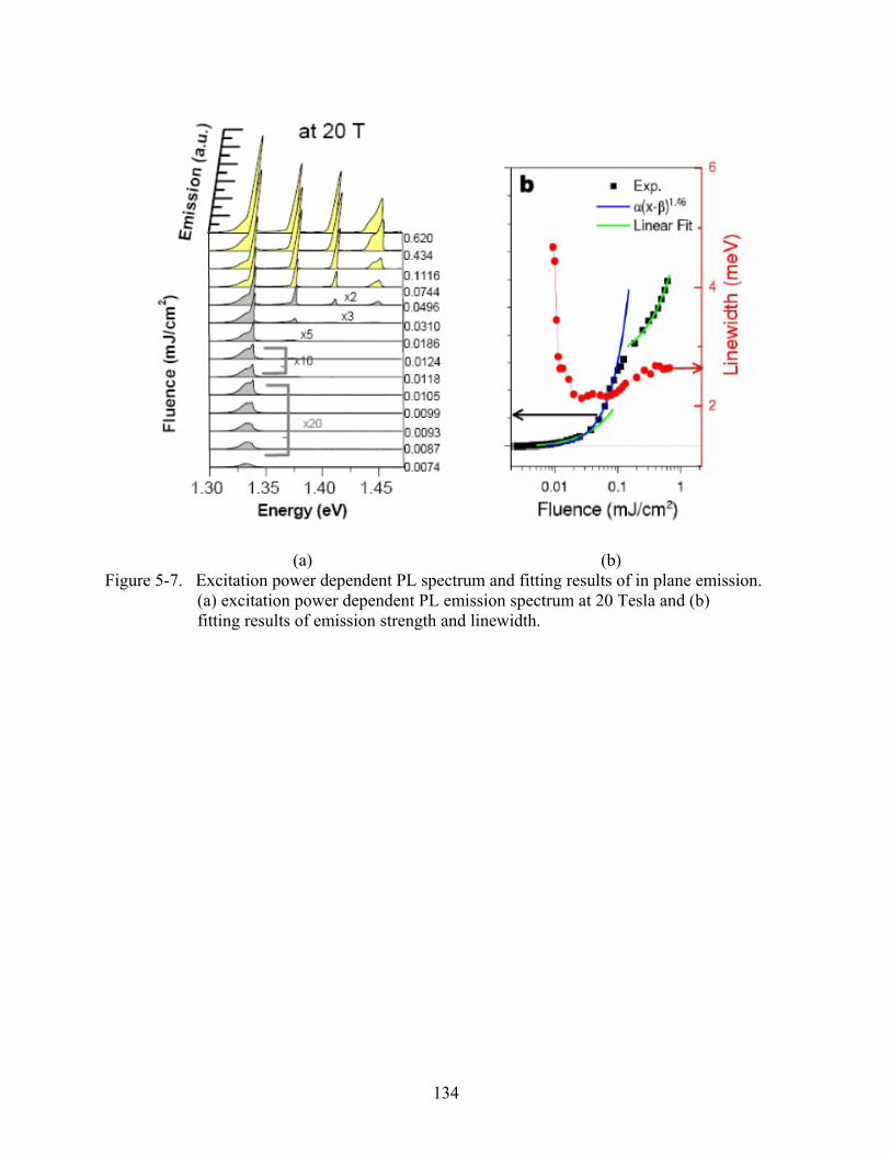
134
(a) (b) Figure 5-7. Excitation power dependent PL spectrum and fitting results of in plane emission.
(a) excitation power dependent PL emission spectrum at 20 Tesla and (b) fitting results of emission strength and linewidth.

135
Figure 5-8. Excitation spot size effect on the in plane PL emission.Emission strength and linewidth of the narrow peak from the 0-0 LL versus (a) B and (b), (c), (d) Flaser for different pump spot size at 20 Tesla. Both B and F are on log scale.
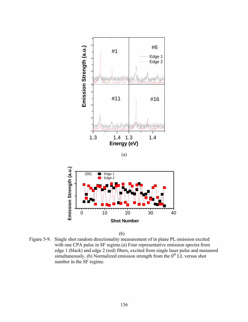
136
Emis
sion
Str
engt
h (a
.u.)
Edge 1 Edge 2
#1
#6
1.3 1.4
Energy (eV)
#16 #11
1.3 1.4
(a)
0 10 20 30 40
Edge 1 Edge 2
Emis
sion
Str
engt
h (a
.u.)
Shot Number
(00)
(b)
Figure 5-9. Single shot random directionality measurement of in plane PL emission excited with one CPA pulse in SF regime.(a) Four representative emission spectra from edge 1 (black) and edge 2 (red) fibers, excited from single laser pulse and measured simultaneously. (b) Normalized emission strength from the 0th LL versus shot number in the SF regime.

137
Emis
sion
Str
engt
h (a
.u.)
Edge 1 Edge 2#1
#6
1.3 1.4
Energy (eV)
#16 #11
1.3 1.4
(a)
0 10 20 30 40
E
mis
sion
Stre
ngth
(a.u
.)
Edge 1 Edge 2
Shot Number
(b) Figure 5-10. Single shot random directionality measurement of in plane PL emission
excited with one CPA pulse in ASE regime.(a) Four representative emission spectra from edge 1 (black) and edge 2 (red) fibers, excited from single laser pulse and measured simultaneously (b) Normalized emission strength from the 0th LL versus shot number in the ASE regime.

138
Figure 5-11. Configuration of control of emission directionality in InxGa1-xAs multiple QW with cylindrical lens.
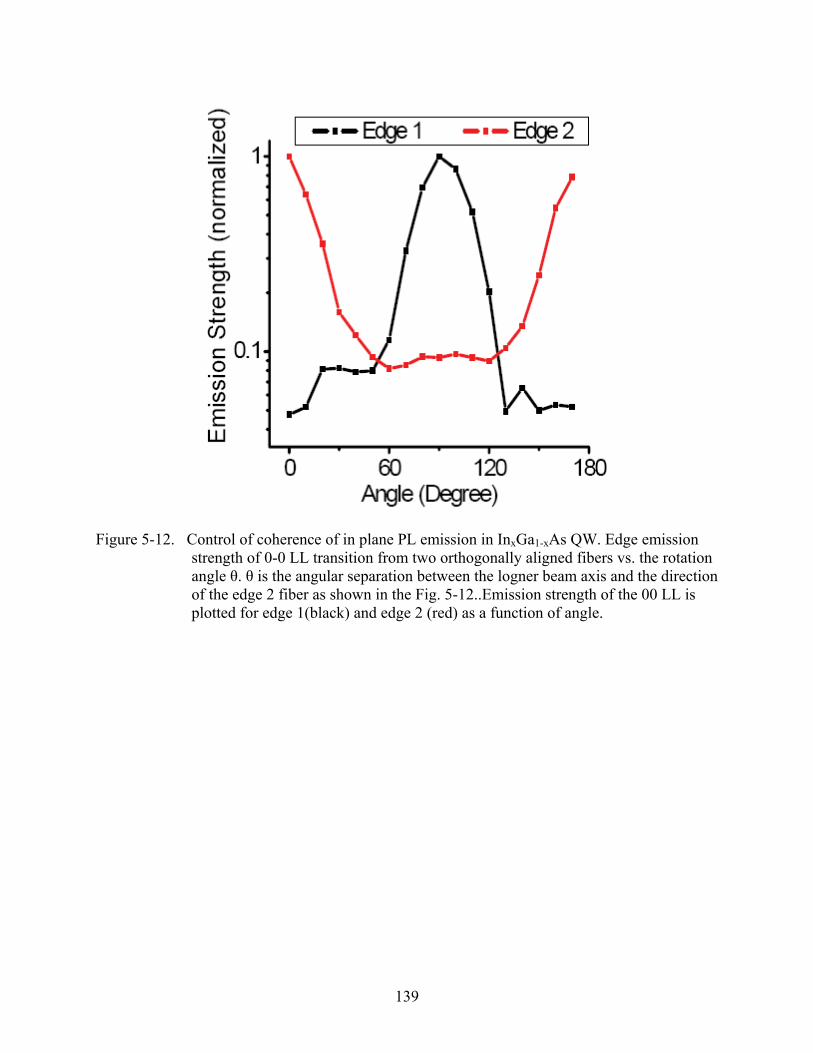
139
Figure 5-12. Control of coherence of in plane PL emission in InxGa1-xAs QW. Edge emission strength of 0-0 LL transition from two orthogonally aligned fibers vs. the rotation angle θ. θ is the angular separation between the logner beam axis and the direction of the edge 2 fiber as shown in the Fig. 5-12..Emission strength of the 00 LL is plotted for edge 1(black) and edge 2 (red) as a function of angle.

140
CHAPTER 6 CARRIER DYNAMICS OF ZINC OXIDE SEMICONDUCTORS WITH TIME RESOLVED
PUMP-PROBE SPECTROSCOPY
6.1 Introduction
The II-VI group wide band gap semiconductor alloys such as ZnO, ZnMgO are recognized
as important materials for potential applications in optoelectronic devices in the ultraviolet
spectral range as well as for integrated optics substrates. Since the exciton binding energy of
ZnO is 60mev [122-126], which is very high compared to GaN (~30mev) [127] or
GaAs(~8mev)[128], the radiative electron hole recombination process in ZnO is even visible at
room temperature[129]. Due to these unique properties, ZnO semiconductor materials are of
interest in applications such as UV light emitting diodes (LEDs) and laser diode (LDs) [130].
Also, ZnO crystal is excellent substrate material for growing another important wide band gap
semiconductor [131-132], GaN, since the lattice mismatch is relative small. For ZnO we have
a=b=3.249oA and c=5.206
oA , while for GaN, we have a=b=3.189
oA and c=5.185
oA .
The dynamics of carriers in ZnO semiconductor, which are critical for high speed electro
optical device design, have recently been investigated by ultrafast time-resolved pump-probe
spectroscopic method or time resolved photoluminescent spectroscopy [133-134] with above
band gap excitation.
In our study, we have performed a comprehensive set of measurements on bulk ZnO, ZnO
epilayers and nanorods. We measured the reflectivity and PL spectra of bulk ZnO, ZnO epilayer
and nanorod from 4.2 K to 70K. In order to understand the excitonic states in ZnO materials,
magneto reflection and PL spectra are also measured at 4.2K. Compared with previous studies
[135], we identify and label the excitonic state on each spectrum. Via spectrally resolved
degenerate pump-probe spectroscopy, we measured the time resolvd differential reflectivity
141
(TRDR) of the A and B excitonic states in bulk ZnO, ZnO epilayer and nanorod. We find the life
time of the A exciton (A-X) is approximately 130ps and while the B exciton (B-X) is ~ 45ps at
for bulk ZnO at 10 K. We also measured the temperature-dependent TRDR of A-X in bulk ZnO
up to 70K, we find that the life time of A-X is still around 100ps, which indicates that relaxation
processes do not change significantly at higher temperatures. This is associated with the
properties of neutral donor bound X (D0X). The life time of A-X (50ps) and B-X(20ps) in ZnO
epilayer are very different from bulk ZnO, which is caused by different neutral donor bound X
(D0X) states in epilaer. The relaxation process of ZnO nanorod is fitted with stretch exponential
decay curve, indicating different relaxation dynamics of Xs from bulk ZnO and ZnO epilayer.
The coherent process in a very short time range (~2ps) on the TRDR of A-X in bulk ZnO is
analyzed with convolution of probe pulse with Gaussian function shape and carriers response
with exponential decay curve.
6.2 Background of Crystal Structure and Band Structure of ZnO Semiconductors
ZnO crystallizes stably in a wurtzite structure with C6v point group symmetry. This typical
semiconductor lattice structure is shown in Fig. 6-1. In the x-y plane, the atoms in a unit cell
form a hexagon, and the zinc atoms form hexagons and oxygen atoms form hexagons stack along
the z-axis, called (0001) direction.
In the x-y plane, since ZnO possesses hexagonal symmetry, many physical and optical
constants are isotropic, while along the z-direction they are different. However, we can use a, b
and c unit vectors to label the unit cell of ZnO, where c is along z-axis and a, b are in x-y plane.
In the study of optical properties of ZnO semiconductors, the polarization of absorption or
emission light are very critical to probe since they are associated with the selection rules of
transition and band structure symmetry. We define π linear polarization parallel to the c axis of

142
ZnO and σ linear polarization perpendicular to the c-axis. The geometry and definitions of
polarization with respect to ZnO unit vectors are plotted in fig. 6-2.
As mentioned in chapter 3, a Hamiltonian with C6v symmetry will couple the s states and
form lowest conduction band and px, py and pz states into three valence bands. The band structure
of ZnO semiconductors is shown in Fig 6-3.
At the center of Brillouin zone, the conduction band is s-like, which has Γ7 symmetry,
while the p-like conduction band splits into three doubly degenerate bands due to spin-obit (Δso)
and crystal-field interaction (Δcr). In the valence bands, the top valence A band has Γ9 symmetry
while the B and C bands have Γ7 symmetry. The excitonic states formed with electron in
conduction band and holes in A, B and C valence bands are called A-X and B-X respectively. In
Fig. 6-3, the total angular momentum (J=L+S, L is orbit momentum and S is spin momentum) of
each Γ points are shown. The A, B and C valence band states at Γ point can be expressed as:
21,
31
21,
31
21,
21:
21,
32
21,
61
21,
23:
21,
21
23,
23:
±+±=±
±−±=±
±±±=±
ZiYXC
ZiYXB
iYXA
mm
mm . 6-1
We can see that each valence band at Γ point are degenerate, each band will split in to doublet
states (spin up“+” and spin down“-”) in magnetic field.
6.3 Valence Band Symmetry and Selection Rules of Excitonic Optical Transition in ZnO Semiconductors
The optical properties of bulk ZnO have been studied for over 40 years, and for the most
part are well understood. However, there remains ambiguity and controversy in the assignment
of symmetries of the A, B and C valence band states. In Thomas and Rodina’s assignment[136-
137], the symmetry of A, B and C valence bands are Γ7, Γ9 and Γ7 since they considered that Pz
143
component is mixed into the A band, which results the reverse of the order of Γ7 and Γ9 in typical
II-VI group semiconductors. In contrast, after carefully studying of the absorption, reflection and
PL spectra as well as the Zeeman splitting of excitonic states of ZnO semiconductor [138],
Reynolds have concluded that the order of top two valence bands in ZnO do not reverse.
Therefore, in Reynolds’s assignment of the order of valence bands in ZnO semiconductor, A, B
and C bands have Γ9, Γ7 and Γ7 symmetry respectively. In this case, A band is pure Px and Py ,
and the only optical transition from A band to conduction band optical transition is expected to
be σ polarization ( ck // and cE ⊥ , k is the direction of light propagation, c is c-axis). For the B
band, the optical transition could be either σ polarization ( ck // and cE ⊥ ) or π polarization
( ck ⊥ and cE // ).
Based on group theory [18], the symmetry and selective rules of optical transition between
conduction band and A, B and C valence bands in ZnO semiconductor are given as follows:
A-X: 5679 Γ+Γ→Γ⊗Γ , 6.2(a)
B-X: 21577 Γ+Γ+Γ→Γ⊗Γ , 6.3(b)
C-X: 21577 Γ+Γ+Γ→Γ⊗Γ , 6.2( c)
where Γ5 is allowed in σ polarization and Γ1 is allowed in π polarization. The optical transition
Γ6 and Γ2 are prohibited and Γ1 is very weak [139].
In order to resolve the controversy of valence band ordering, a magnetic field was
employed to observe Zeeman splitting of different optical transitions, since the Zeeman splitting
for 79 Γ→Γ transition and 77 Γ→Γ transitions are very different--Γ6 is a doublet and splits into
two in magnetic field while Γ1 is a singlet and does not split in a magnetic field. Reynolds
clarified the symmetry of the top valence band by studying the splitting behavior of PL emission

144
line from A-X in magnetic filed at configuration [139]. In this thesis, we will consider the order
of valence band according to the Reynolds assignment.
6.4 Impurity Bound Exciton Complex (I line) in ZnO and Zeeman Splitting
In bulk semiconductor materials there are many types of defects and localized states. Some
of these states can bind excitons, resulting in a bound exciton complex (BEC).
Conceptualizations of an exciton bound to an ionized donor (D+X), a neutral donor (D0X) and a
neutral acceptor (A0X) are plotted in Fig.6-4. The binding energy E of these bound excitons
usually increases according to [40]
XAXDXD EEE 00 <<+ . 6-3
These BECs have many emission lines in the PL spectrum of bulk ZnO, termed ‘I’ lines. Also,
when the free excitons or BEC optical transitions couple with longitudinal optical (LO) phonon,
the phonon replica can be observed in the PL spectrum at energy position
LOmEE ωh−=' , 6-4
where E’ is the positions of phonon replica, E is the energy of optical free exciton or BEC
transition which is coupled with LO phonons, m is an integer, and LOωh is energy of LO phonon.
However, these phonon replica emission peaks are usually much weaker than the BEC emissions
or free X emissions.
In a magnetic field, a quantum state with spin will split into two states, spin up and spin
down. The energy splitting between the two states are called Zeeman splitting. However, in the
case of free excitons or BEC, both electrons and holes can be involved in Zeeman splitting,
which makes the interpretation of energy splitting of ZnO semiconductor in magnetic field more
complicated than free electrons.
Zeeman splitting in ZnO can be express as

145
BgE excμ=Δ , 6-5(a)
where μ is Bohr magnon, B is magnetic field strength and gexc factor is Lande factor and can be
written as:
heexc ggg += . 6-5 (b)
For an electron, the g factor is isotropic, while for a hole the g factor is anisotropic (g// and g⊥),
and typically g⊥ is nearly zero [136]. In above expression, // means the c-axis of ZnO is parallel
to the magnetic field B and ⊥ means the c-axis is perpendicular to the magnetic field.
In the case of BEC, the Zeeman splitting is qualitatively different than free excition
Zeeman splitting since the splitting of ground states of D0 and A0 has to be considered in addition
to the splitting of electron and hole in an exciton. Rodina and Reynolds [139] have studied the
splitting of BEC in ZnO and the results are shown in Fig. 6-5.
As shown in figure 6-5, the excited state of D0X consists of a donor defect, two electrons
and one hole, with the two electrons spins antiparallel. The Zeeman splitting of the excited state
is determined by the anisotropic hole effective g factor, while the Zeeman splitting ground state
D0 is given by the effective g factor of electron ge. Therefore the splitting of optical transition of
D0X in the Faraday geometry (B//c and k//c) (see Fig.6-6) is given by
BggE he μ)( //−=Δ , 6-6(a)
and the splitting in Voigt geometry (B⊥c and k//c) (see Fig.6-6(b) )is
BgE eμ=Δ . 6-6(b)
Also the Zeeman splitting should be linear in magnetic field. In the case of the acceptor bound
exciton A0X, the Zeeman splitting has similar form.
146
6.5 Samples and Experimental Setup for Reflection and PL Measurement
The ZnO samples we used for magneto optical spectroscopic studies are bulk ZnO (grown
by MTI Crystal Co.), ZnO epilayers (grown by David Norton’s group at University of Florida),
and ZnO nanorod grown in GIST in South Korea). The size of bulk ZnO is 5x5x0.5mm and the
orientations of the crystals are c-plane (c-axis perpendicular to the plane) or a-plane (a-axis
perpendicular to the plane and c-axis in the plane) configurations. The bulk ZnO crystal was
grown with hydrothermal method. The 400nm thick ZnO epilayer samples were grown on a c-
plane sapphire substrate via the MBE method and the self-assembly ZnO nanorod sample with
rod diameter 8nm is grown with laser deposition. All the ZnO samples were nominally undoped.
We measured the reflection spectrum of all the ZnO samples with polarized light to
identify the excitonic states. We used a Deutrium lamp with the output polarized using a Glan-
Laser polarizer. In the reflection spectrum measurements, ZnO samples were put in a cold finger
style optical cryostat, in which the samples can be cooled down to 4.2K with liquid helium.
In magneto-optical spectrum measurements, we used the cw magneto-optical facility at
NHMFL shown in Fig.2-2, 2-3. The ZnO was mounted inside the helium tail of a Janis cryostat
and cooled down with helium exchange gas. The light was delivered to ZnO sample through
multimode optical fiber, and the reflection and PL emission were collected with another
multimode optical fiber. Here, we used a UV Xenon lamp for measuring the reflection spectrum
and a He-Cd laser (325nm wavelength) for exciting the sample to measure the PL spectrum.
Both the reflection light and PL emission were delivered to a 0.75m McPherson spectrometer
and the spectrum was recorded with a charge-coupled device (CCD). In the temperature
dependent measurement, the sample temperature was measured and controlled by a Cernox
sensor, a Cryocon temperature controller and a heater with 50 W maximum power output.
147
6.6 Results and Discussion
In figure 6-7, the reflection spectrum of a-plane bulk ZnO at 4.2K obtained using σ and π
polarized light. The excitonic optical transitions obey the transition rules listed in equation. 6-2,
where A-X (Γ9), B-X (Γ7) and C-X (Γ7) are activated in σ polarized light and C-X (Γ7) is
activated only in π polarized light. However we cannot specify the exact energy positions of free
excitons peaks since the complexity in reflection spectrum (see Chapter 2).
In figure 6-8(a), the magneto-PL spectrum of c-plane bulk ZnO is plotted for the Faraday
configuration (B//c, k//c, E⊥c). We can see that the PL emission feature is a sharp peak sitting on
the top a broader and weaker peak, which caused by inhomogeneous broadening. There is no
significant magnetic splitting observed, although the sharp PL peak becomes broader (possibly
due the onset of splitting) and the PL intensity becomes lower with the increasing of magnetic
field strength. Figure 6-8(b) shows the PL spectrum of the same sample at Voigt configuration
(B⊥c, k//c, E⊥c). It is clearly evident that the sharp PL peak split linearly into two peaks with the
increasing magnetic field. The energy position vs. magnetic field of the peaks is plotted in figure
6-8(c). This is Zeeman splitting and will be discuss further in the following section, however,
since we use multi-mode fiber to delivered light, no polarization information can be obtained
from the two PL peaks and the spin states can be resolved.
In order to understand the PL emission spectrum, we plot the reflection and PL emission at
zero field in figure 6-9(a). We can assign the PL emission peak at 3377 meV to the
recombination of free A-X, indicated by an arrow in the figure. The other PL peaks at lower
energies are assigned as emission from impurity bound A-X, the strongest bound exciton PL
peak is at 3360 meV and has been reported to be neutral donor bound exciton (D0X) [140].

148
In figure 6-9(b), the reflection and PL emission spectrum of the c-plane bulk ZnO in both
Faraday and Voigt configurations at 30 Tesla are plotted. From this data, we can conclude that
the A-X and its bound state do not split in Faraday geometry while they split into two peaks in
Voigt geometry. At 30 T, the splitting of PL peaks from A-X donor bound state is ~3.4 meV.
The magnetic splitting of A-X and D0X can be interpreted with the splitting process shown
in figure 6-5 and equation 6-6 as following. In the Faraday geometry, according to Eq. 6-6, the
magnetic Zeeman splitting of A-X and D0X is determined by Lande factor gexc, which is ge-
gh=0.7[16], therefore the Zeeman splitting at 30 Tesla is around 1.2 meV, which is smaller than
the resolution of spectrometer and thus can not be observed with our spectrometer.
However, in Voigt geometry the Lande factor gexc=ge, since gh=0, therefore the Zeeman
splitting at 30 T is ~3.38 meV, which is in agreement of our observation 3.08 meV. In Fig.6-
8(d), we plot the experimental and calculated results of ΔE vs. B, the results are in good
agreement if we take into consideration that the resolution of spectrometer is around 1meV. This
agreement strongly proves that the dominant PL emission peak comes from neutral bound
exciton.
In the case of the ZnO epilayer sample, we plot the reflection and PL spectrum at zero
fields in figure 6-10(a), we can clearly resolve the A-X and B-X in the reflection curve. In the PL
spectrum we observe a strong emission at 3355 meV, which is also from bound exciton
transition, however the PL peak is asymmetric and has a long tail at the low energy side, and in
addition the PL linewidth is much broader (5~6 meV) than the bulk ZnO (2 meV). All of these
observations imply that the optical quality of this ZnO epilayer is not as good as bulk ZnO, with
more defect states present which cause more inhomogeneous broadening and carrier trapping
below the bandgap, and result in the PL linewidth broadening and an asymmetric line shape. At

149
3285 meV, we observe a PL emission peak due to LO phonon coupled with bound exciton
transition, since the LO phonon energy is 70 meV in ZnO. Due to the fact that the PL emission
linewidth is larger than the predicted Zeeman splitting, we cannot resolve and observe the PL
peak splitting in neither Faraday geometry nor Voigt geometry in this ZnO epilayer sample as
shown in Fig.6-10(b).
6.7 Time Resolved Studies of Carrier Dynamics in Bulk ZnO, ZnO Epilayers, and ZnO Nanorod
As introduced in chapter 2, time resolved spectroscopy is a very important tool for
understanding the dynamics of carriers and excitons in semiconductors, critical for applications
in electro- optical device.
From Chapter 2, the changes to the dielectric fuction ε are given by [141]
∑Δ−=Δ
i Li
iL m
etNt 20
2)(),(ωε
ωε . 6-7
Where ωL is the laser frequency, )(tNiΔ is the carrier density in the ith energy band and mi is the
carrier mass of the ith band. Since ZnO is a wide bandgap semiconductor, the high-frequency
limit (ωLt>>1) is satisfied, therefore the differential reflectivity is proportional to the change in
carrier density in each energy band divided by the mass of the band, summed overall bands,
which is shown in equation 6-8,
∑ΔΔ
i i
i
mN
RR )(~ . 6-8
This shows clearly that the differential reflectivity measurements effectively probe the changes
in carrier density in different ZnO energy bands.
In the recombination of an electron and hole pair, both radiative and nonradiative
recombination processes are usually involved, and the rate equation can be expressed as follow
150
venonradiatiradiative
AAdtdN
N ττ211
+= , 6-9
where N is the carrier density, radiativeτ and venonradiatiτ are radiative and nonradiative relaxation
times, 2A 2A is corresponding efficiency. In radiative recombination, photons are emitted as the
carriers recombine to conserve energy, while in nonradiative processes, electrons and holes
recombine through emission of acoustic phonons.
As we have seen that bulk and epilayer ZnO exhibit different reflectivity and photo-excited
emission characteristics due to the presence of defect states, we now turn to investigations of
how those differences impact dynamical carrier processes. We measured the time resolved
differential reflectivity (TRDR) spectrum of ZnO semiconductors, including bulk with different
orientation, c-plane epilayer and nanorod samples with 8 nm rod diameters. Since the absorption
coefficient of ZnO is very high, it is very difficult to get good transmission signal from thick
samples, we use reflection geometry to get TRDR signal.
The experimental setup for measuring the TRDR of ZnO semiconductors is shown in
figure 6-11. We used ultrafast laser pulses 150fs in duration at a wavelength of 730 nm from a
Coherent Mira 900-F laser system with 76 MHz repetition rate. The laser beam was focused onto
a nonlinear β-barium-borite (BBO) crystal to frequency double the pulses into the near UV
around 365nm via second harmonic generation (SHG). The UV laser pulses were then split into
pump and probe beams using a sapphire plate. Both the pump and probe beam propagated
through waveplates and Glan-Laser polarizers to make them parallel or perpendicularly polarized
before they were focused down to 50μm on the ZnO samples, mounted in an optical cryostat.
Liquid helium flows into the cryostat during the measurements, by which we can cool down the
ZnO samples to down to 4.2K and reduce the thermal broadening effect and phonon effects. The

151
pump beam was time delayed with respect to probe beam using a Newport stage controlled by
computer. To obtain the best signal-to-noise ratio, the pump and probe beams were chopped with
a differential frequency f1 = 2KHz and f2 = 1.57KHz, and the probe reflectivity signal was
detected using photodiode via a lock-in amplifier demodulating the signal at f1-f2.
6.8 Experimental Results and Discussion
6.8.1 Relaxation Dynamics of A-X and B-X in Bulk ZnO
In figure 6-12, the TRDR at 10K are plotted for A-X and B-X in a-plane bulk ZnO
semiconductor, both the probe beam and pump beam set to σ polarization (perpendicular to c-
axes), in which A-X and B-X are optically activate. The DR curve decays exponentially. We fit
the two curves exponentially with equation 6-9 and obtain the following results,
psAX 10130 ±=τ and psBX 145 ±=τ .
The sharp peaks in figure 6-12(a) and (b) at t=0 ps most likely arises from a coherent
artifact due to the collinearity of the pump and probe polarization. More discussion about this
fast relaxation process will be given in the following.
However, the relaxation time τ is much smaller than previous report for free A and B
excitons [142], reported 1ns. This strongly suggests that in these samples, the A and B excitons
are mainly bound to an impurity state, which makes the D0X dominate the relaxation process
instead of free exciton recombination. This agrees well with the PL data (figure 6-9) in which the
D0X is three orders stronger than free A-X. In this case, 1A is much smaller than 2A , which
indicates that the radiative recombination can be neglected compared to nonradiative processes
in the exciton relaxation process.
In figure 6-14, we plot the TRDR spectrum of AX in c-plane bulk ZnO at different
temperatures up to 70K, where the laser wavelength is tuned to resonantly probe the A-X as the
152
temperature increases. The artifact observed in figure 6-12 does not show up here because the
pump and probe laser beam are orthogonally polarized. We also observe mono-exponential
decay of DR in this figure. The fitting results of the relaxation time are psAX 10130 ±=τ , which
do not change significantly with temperature up to 70K and imply that the A-X relaxation
process is dominated by a bound to impurity state instead of radiative recombination up to 70K,
since the binding energy between neutral donor and an exiton is around ~10meV [18], which
makes it difficult to break them at low temperature.
In semiconductor, immediately after the carrier are excited with coherent laser light (pump
beam), the carriers preserve the coherence generated with laser beam in a very short time (~ps)
[143], if the probe beam arrives during this carrier coherent status, strong interaction will be
expected between the coherent carriers and coherent light, which result in the sharp feature in
Fig. 12. In this case, the actual signal that we acquired is the convolution of probe pulse and
carrier decay, which are presumed to be Gaussian function and exponential decay function
respectively. The convolution result is given as:
⎟⎠
⎞⎜⎝
⎛−−−=
στσ
ττσ
221)[
2exp(
2)( 2
2 terftAtS . 6-10
Where τ is the exponential decay time and 2 σ is the FWHM of the Gaussian function.
Fig. 6-13 shows the fitting of the fast relaxation cure with the convolution function 6-10, we can
see that the pulse width is around 0.5ps and the coherence exponential decay time is around
1.4ps.
6.8.2 Relaxation Dynamics of A-X and B-X in ZnO Epilayer and Nanorod
In figure 6.-15, TRDR spectra of AX and BX in ZnO epilayer at 4.2K are plotted. It is
clearly resolved that the carriers populate on BX decay mono-exponentially. The fitting result of
153
BX relaxation time is τ BX ps= ±25 1 .however the A-X shows a stretched exponential decay
process, which is described by
0exp ItAIn
+⎟⎠⎞
⎜⎝⎛−=
τ, 6-11
where τ is the decay time and n<1 is stretched factor.
With this function, the fitting results of A-X relaxation in ZnO epilayer are n=0.9 and
τ=50ps.These exciton relaxation times are much smaller than the bulk ZnO, which indicate that
the density of defect states in the ZnO epilayer sample are more than that in the bulk ZnO
sample. Also, by comparing the carrier relaxation time, we might expect that the defect state
dominates in epilayer sampler should be different from that in bulk sample since the relaxation
are quite different. These can be convinced in the PL spectrum in figure 6-10, in which we can
not see the free X emission, most Xs are bound to defect states and emit photons at 3355 meV in
stead of 3360 meV in bulk ZnO samples.
In figure 6-16, the TRDR of ZnO bulk nanorod is shown. The excitation and probe light
energy is 3416mev, which is supposed to be above the ZnO bandgap. We can see that the TRDR
cure of ZnO bulk nanorod sample decay stretched exponentially. This curve is fitted with 6-11.
The fitting results are τ=17ps and n=0.65.
The stretched exponential relaxation is summation of distribution of independent
exponential decay relaxations and is indication that there is an inhomogeneous distribution of
recombination times. It is reported in many semiconductors material especially in nanostructures
[144-145]. Three mechanisms [146-147] are proposed to interpret the stretched exponential
decay.
The distribution in lifetime is a result of varying carrier localization such that carriers can
escape from one area of sample to other area and recombine nonradiatively.

154
The migration of excitons between distorted nanostructures is possible, which result in the
capture and delayed released of excitons.
Distribution of the lifetime in PL at a single wavelength could be explained by the
distribution of the nanocrystal shapes in a given area.
From the above explanations, we found that the stretched exponential is mainly caused by
the either trapped of carriers, carrier hopping between nanostructures or different size of
nanostructures.
We can see that the stretched exponential decay of exciton in ZnO epilayer and nanorods
indicate that the sample might have many defects states, which traps the carriers, the nanorod
sample might have different size effect and also the carriers in nanorod might migrate between
rods.

155
Table 6-1. Some parameters of ZnO bulk semiconductors Point group 6mm(C6v) (Wurtzite) Lattice constants at room temperature a=3.250, c=5.205 nm1 Electron mass 0.28 m1
e Hole mass 1.8 me
1 Bandgap energy at room temperature 3.37 eV1 Exciton binding energy 60 meV1 Melting point 2250 K1 LO phonon 70 mev1 1 Reference[10]

156
Zn atom on the top layer
Zn atom on the bottom layer
O atom
y
xz
Figure 6-1. Top view of the lattice structure of a wurtzite ZnO crystal. In the x-y plane, ZnO has hexagonal symmetry along the z-axis. In z-axis direction, Zn atoms are on the top and bottom layers, O atoms layer is between the two Zn atom layers. Also, another O atoms layer (not shown) is on the top of top layer of Zn atoms. In the (0001) direction, hexagonal symmetry is along the z-axis.

157
Figure 6-2. The orientation of light polarization with respect to the ZnO unit cell. The σ polarization is defined as perpendicular to c-axis and π polarization is defined as parallel to c-axis.
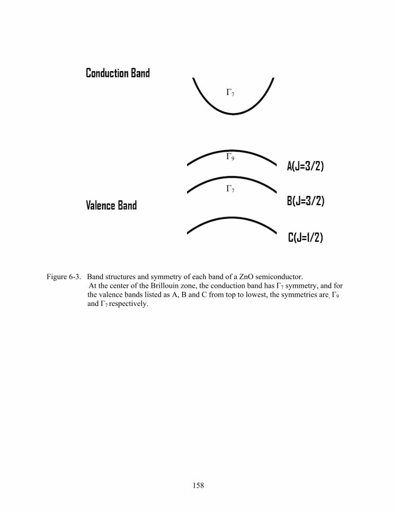
158
Figure 6-3. Band structures and symmetry of each band of a ZnO semiconductor.
At the center of the Brillouin zone, the conduction band has Γ7 symmetry, and for the valence bands listed as A, B and C from top to lowest, the symmetries are, Γ9 and Γ7 respectively.
Γ9
Γ7
Γ7

159
(a) D+X
(b) D0X
(c) A0X
Point defect electron hole
Figure 6-4. Schematic of types of impurity bound exciton complexes. (a) an ionized bound exciton (b) a neutral donor bound exciton (c) a neutral acceptor bound exciton

160
(a)
(b)
Figure 6-5. Energy diagram of Zeeman splitting of neutral bound excitons in ZnO. (a) donor-bound exciton, (b) acceptor-bound exciton
gh⊥=0
(D0, X)
(D0) ge=1.95
B⊥C B//C
+1/2 -1/2
+3/2 -3/2
gh=1.25
+1/2 -1/2
+3/2 -3/2
gh⊥=0
ge=1.95 (A0, X)
(A0)
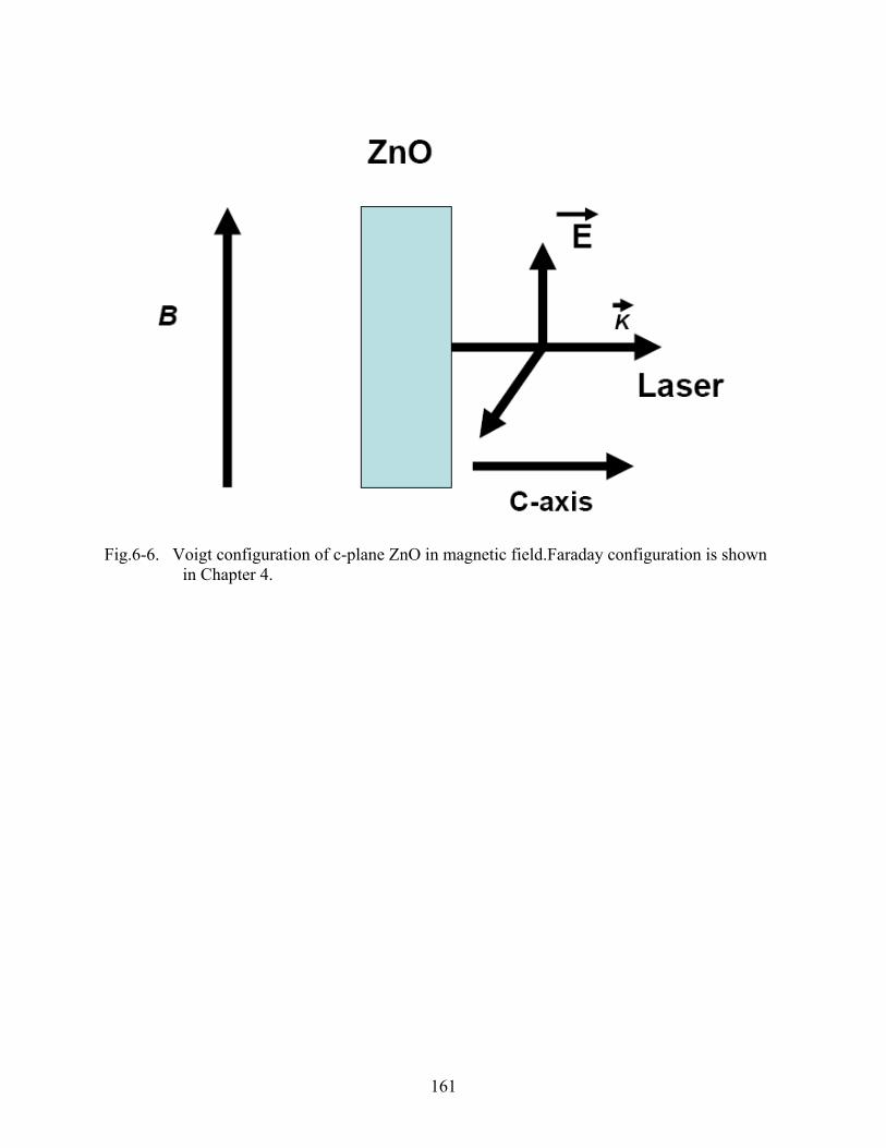
161
Fig.6-6. Voigt configuration of c-plane ZnO in magnetic field.Faraday configuration is shown in Chapter 4.
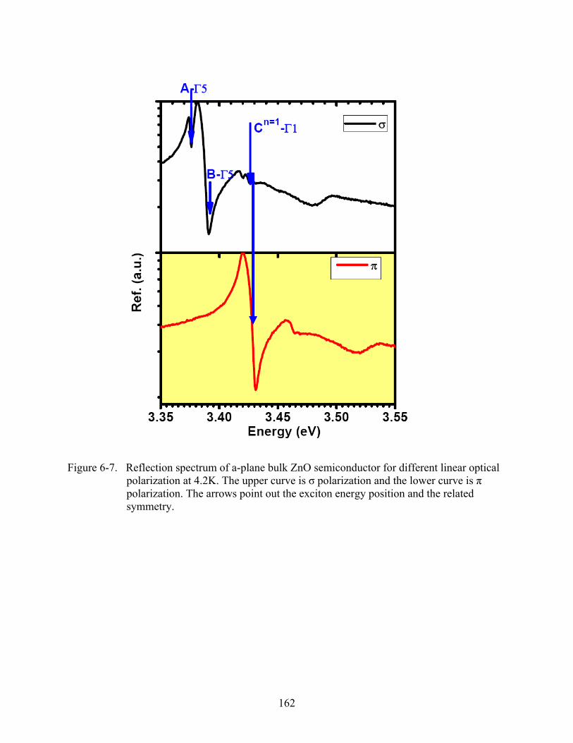
162
Figure 6-7. Reflection spectrum of a-plane bulk ZnO semiconductor for different linear optical polarization at 4.2K. The upper curve is σ polarization and the lower curve is π polarization. The arrows point out the exciton energy position and the related symmetry.

163
(a) (b)
(c) (d) Figure 6-8. The magneto-PL spectrum of a and c-plane bulk ZnO sample and Zeeman splitting
at 4.2K PL spectrum in (a) Faraday and (b) Voigt configurations, (c) The Zeeman energy splitting in Voigt geometry as function of magnetic field, (d) Zeeman splitting ΔE vs. magnetic field, black dot is experimental result and red and blue line are fitting with g=1.95 and 2.0 respectively.

164
3300 33 50 3400 3450
100
1000
1 0000
10 0000
R eflec tiv ity
P L
FX
3360m ev
3377 m ev
D 0X
Energy (m ev)
PL
Inte
nsity
AX
(a)
3300 3350 3400100
1000
10000
100000
Energy (mev)
PL
Inte
nsity
FX
D0X
AX
(b) Figure 6-9. Comparison of reflection and PL spectrum of c-plane bulk ZnO. (a) reflection
(black curve) and PL (red curve) at zero magnetic field, (b) reflection in the Faraday geometry (black curve), Voigt geometry (red curve), and PL in the Faraday (green curve) and Voigt (blue curve) configurations at 30 T.

165
3 2 5 0 3 3 0 0 3 3 5 0 3 4 0 01 0 0
1 0 0 0
1 0 0 0 0
1 0 0 0 0 0
3285mev
PL In
tens
ity
A-X
B-X
3355mev
Bound X-LO Phonon
Energy (mev)
D0X
(a)
3250 3300 3350 3400 3450100
1000
10000
100000
PL In
tens
ity
BX
AX
Bound X
Energy (mev)
(b)
Figure 6-10. Comparison of reflection and PL spectrum of c-plane epilayer ZnO at 4.2 K. (a) reflection (black curve) and PL (red curve) at zero magnetic field, (b) reflection in the Faraday geometry (black curve), Voigt geometry (red curve), and PL in the Faraday (green curve) and Voigt (blue curve) configurations at 30 T.

166
Figure 6-11. Pump-probe experimental setup for measuring TRDR of ZnO semiconductors. BS
is beam splitter, WP is waveplate, G-L is Glan-Laser polarizer, PD is photodiode
Dichroic mirror
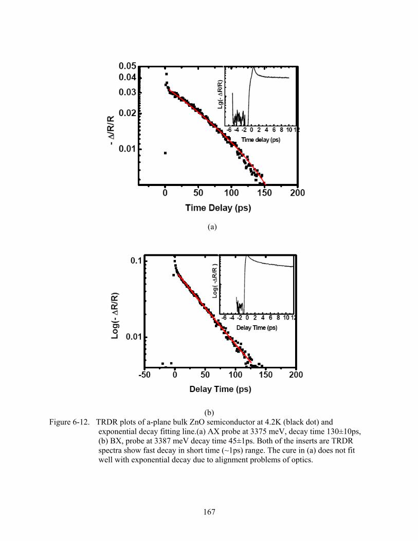
167
(a)
(b)
Figure 6-12. TRDR plots of a-plane bulk ZnO semiconductor at 4.2K (black dot) and exponential decay fitting line.(a) AX probe at 3375 meV, decay time 130±10ps, (b) BX, probe at 3387 meV decay time 45±1ps. Both of the inserts are TRDR spectra show fast decay in short time (~1ps) range. The cure in (a) does not fit well with exponential decay due to alignment problems of optics.

168
-0.6 -0.3 0.0 0.3 0.6 0.9 1.2 1.5
TR
DR(-D
R/R
)
Time Delay (ps)
Figure 6-13. Fast decay in TRDR of A-X in a-plane bulk ZnO and the fitting with convolution of Gaussian function probe pulse and exponential decay response function. Fitting parameters are pulsewidth=0.5ps and τresponse=1.4ps.

169
0 20 40 60 80 100 120 140 160
10K 20K 30K 50K 70K
Log(
-ΔR
/R)
Time Delay (ps)
Figure 6-14. Temperature dependent TRDR of A-X recombination in c-plane bulk ZnO. Probe
wavelength is tuned to the A-X resonant wavelength. The fitting results of decay time τ=130ps do not change significantly with the temperature increasing.
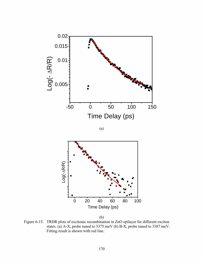
170
-50 0 50 100 150
0.005
0.01
0.015
0.02
Log(
- ΔR
/R)
Time Delay (ps)
(a)
0 20 40 60 80 100
Log(
-ΔR
/R)
Time Delay (ps)
(b) Figure 6-15. TRDR plots of excitonic recombination in ZnO epilayer for different exciton
states. (a) A-X, probe tuned to 3375 meV (b) B-X, probe tuned to 3387 meV. Fitting result is shown with red line.

171
0 40 80 120 160 2001E-3
0.01
T=10K
Log(
- ΔR
/R)
Time Delay (PS)
Figure 6-16. Experimental TRDR plot of ZnO nanorod sample at 10K and fitting result with a
stretched exponential decay. Black dots are experimental results and red curve is fitting results with a stretched exponential function. Fitting parameter are τ=17±1ps and n=0.65±0.01.
172
CHAPTER 7 CONCLUSION AND FUTURE WORK
In order to study the carriers dynamics of III-V group semiconductor quantum wells at
high carrier density (~1012cm-2) and high magnetic fields, we have developed an ultrafast optics
facility at the National High Magnetic Field Laboratory, including an ultrafast chirped pulse
amplifier, optical parametric amplifier, and a 17.5 Tesla superconducting magnet (SCM3) as
well as the necessary cryogenic system and optical probes for both SCM3 and the 31 T Bitter
magnet in cell 5. This unique facility provides us high power pulses (GW/cm2) in broad
wavelength range (200nm to 20μm) and high magnetic fields (up to 31 Tesla) to study the
quantum optics of e-h pair in semiconductor quantum wells. A detailed description of this
facility was shown in Chapter 2.
To understand the optical transmission and reflection spectrum of semiconductors, we
gave a detailed description of the optical response theory. In addition, the detailed theory of the
electronic states in semiconductor quantum well is given as well as the excitonic states and LL
splitting in high magnetic field was presented.
With these as a background, this dissertation has presented a systemic spectroscopic study
of magneto-optical properties of InxGa1-xAs/GaAs multiple quantum well in the low and high
excitation regimes using CW light source high excitation domain with a high power ultrafast
light sources at magnetic field up to 30 T.
In low excitation regime, we can clearly resolve the interband LL transitions originating
from the same conduction and valence subbands in the absorption spectrum of InxGa1-xAs/GaAs
multiple quantum wells at 4.2K to 30 T. Anticrossing phenomena and dark excitonic states are
shown between the traces of e1h1ns and e1l1ns magneto excitonic states. Theoretical calculation
shows that this larger splitting (~9 meV) does not arise from valence band complexity.

173
In high excitation regime, we measured PL emission from InxGa1-xAs/GaAs multiple
quantum wells excited with high power CPA pulses (~GW/cm2). We do not see Coulomb
interaction-induced anticrossing between LL levels originating from heavy holes and light holes.
Bandgap renormalization is clearly observed when we compared the Landau fan diagrams of
absorption spectrum in low excitation and PL spectrum in high power regime. Both of these
indicate that Coulomb interaction in e-h pair is screened at high carrier density (~1012/cm2) and
PL from high density e-h plasma dominates the out-of-plane PL emission at high field and high
excitation.
In the high power excitation spectrum of InxGa1-xAs/GaAs multiple quantum well, we
observed strong and sharp features on the PL peaks, suggesting the study of amplified emission
processes in the InxGa1-xAs/GaAs MQWs. With the ultrafast facility developed at NHMFL, we
were able to study the in-plane PL emission from InxGa1-xAs/GaAs MQWs. We observed
abnormally strong emission. By measuring and analyzing the field dependent, power dependent
PL spectra and the single pulse excited PL spectra, we characteristized this sharp peak emission.
(I) the PL emission strength of sharp peak increased linearly above a certain magnetic field (13
T) or laser fluence (0.01 mJ/cm2) associated with an ASE process. (II) above a critical magnetic
field (~16 T) or laser fluence( ~0.03 mJ/cm2 ), the PL strength increases super linearly (~B1.5 or
F1.5), (III) for single pulse excitation above the fluence threshold, we collect the in-plane PL
emission for different propagation directions, and the single shot experiment shows
anticorrelated emission between the PL strength at different directions. However, for the single
pulse excitation experiment, we observed a complete correlation between in-plane PL at different
propagating directions, consistent with ASE emission. With an understanding of the cooperative
theory of light emission introduced in detailed in chapter 5, we found that the characteristics of
174
strong PL above magnetic field or fluence threshold from in-plane emission are consistent with
the cooperative emission process--superfluorescence, in which all the excited carrier are coherent
during the emission process and give a very short burst emission of coherent light.
This dissertation also presents comprehensive spectroscopic investigations on ZnO
semiconductors, including bulk, epilayer and nanorod samples. The A and B excitonic states are
clearly identified in the reflection spectra with optical selection rules. PL from donor or acceptor
bound excitons dominates the emission spectrum up to 70K in the bulk ZnO and ZnO epilayer.
To understand the excitonic states of ZnO in more detail, we measured the PL spectrum at high
magnetic field up to 30 Tesla. Zeeman splitting form donor bound excitons is clearly resolved
and analyzed with theoretical predication, we found that in Voigt geometry, the effective Lander
factor is g~2, which is close to theoretical predication.
Ultrafast time resolved pump-probe experiments are also carried to study the A-X, B-X
dynamics in bulk ZnO, ZnO epilayer as well as ZnO nanorod. Exponential decay is observed in
A-X (~130 ps) and B-X (~50 ps) in bulk material, which is corresponding to relaxation to D0X.
In epilayer and nanorod sample, we observed stretched exponential decay process, (n=0.9 and
τ=50 ps for A-X for the epilayer, n=0.6, τ=17 ps for the nanorods), related with carrier hopping
transport and carrier localization.
For the future, we need to obtain the time resolved information of the cooperative
recombination process in high density e-h plasma in high magnetic field, including measuring
the SF pulse width, time delay for evolution of coherence between atoms. We proposed the
following experiments:
• Time resolved pump-probe experiment to measure the carrier dynamics in InxGa1-
xAs/GaAs QW at high magnetic fields. This can be done with the CPA and OPA.

175
• Time resolved PL from in-plane emission in QW at high magnetic field, this can be done
with streak camera and provide us the time information of evolution of coherence.
• Upconversion PL measurement of SF from InxGa1-xAs/GaAs QW in high magnetic field,
this can provide us the time information of the pulse width of SF.
As for the ZnO semiconductor, we propose to perform time resolved PL measurements
with a streak camera, which can provide more information of the radiative and nonradiative
dynamics of exciton and bound excitons.
176
APPENDIX A SAMPLE MOUNT AND PHOTOLUMINESCENCE COLLECTION
A commercial Janis cryostat (shown in Fig.2-8) is modified for sending fs laser directly on
the sample cooled down to 10K inside the cryostat. On the tail of modified optical cryostat
shown in Fig.2-10, an optical window is mounted on the bottom of the cryostat outer tail. Fig. A-
1 shows the detailed configuration of the sample mount, optical fiber and PL collection used in
the experiments.
The sample mount, which is made of cooper, is bolted on the bottom of liquid helium tail
of the cryostat. An indium foil is used between the sample mount and the bottom of liquid
helium tail for better heat conduction. With this method, the sample can be cooled down to
around 10K.
The InxGa1-xAs/GaAs MQW is positioned on the top of a sapphire plate, which is about
1mm thick. Special optical glue is used to firmly attach the sample on the sapphire plate. This
optical glue is transparent for visible and near infrared light, which is suitable for 800nm CPA
excitation light and the PL emission around 930nm. The optical glue is dried with strong UV
light heater. A right prism with size 1mmx1mm is also attached to the sapphire plate and one
edge of the InxGa1-xAs/GaAs MQW. The sapphire plate with sample on it is positioned on the
cooper sample mount with GE varnish, special glue with good conductivity at low temperature.
A Cernox temperature sensor is attached to the sample mount right beneath the sapphire plate, so
that the temperature of sample can correctly measured. An electric heater is also position around
the sapphire plate for temperature control.
Two optical fibers are inserted into the small tubing inside the liquid helium and go
through the bottom of the helium tail, indium foil and sample mount, and reach the sapphire
plate. The sapphire is positioned well so that the two fibers are right on the top of the center of

177
sample and the top of right angle prism respectively. The fiber on the center is used to collecting
the PL emitted perpendicular to the quantum well plane while the fiber on the prism is used for
collecting the PL propagating inside the quantum plane, the in plane PL is coupled into the fiber
with the prism. Strong white light is induced to the fibers from the open end to find the best
positions of the other ends of optical fiber on the top of sapphire plate.

178
Optical fiberedge collection
Optical fibercenter collection
Liquid Helium tailLHe LHe
Indium foil
Cernox temperature sensor
HeaterHeater
Sapphire plate
Right angle prism
InxGa1-xAs/GaAs QW
Stainless steel tubing
Sample mount
Figure A-1. Detailed schematic diagram of sample mount and PL collection used in the experiment.

179
APPENDIX B PIDGEON-BROWN MODEL1
In a realistic calculation of electronic states in semiconductor in magnetic fields,
p•k theory [71] is required to for good approximation of the bandstructure. For narrow gap
semiconductors such InGaAs or InAs, the coupling between the conduction and valence bands is
strong, so it is necessary to calculate the LLs with eight-band model. Pidgeon and Brown [94]
develop a model to calculate the LLs in magnetic field at k=0. This model is generalized to
include the wave vector ( 0≠k ) in this chapter.
The wave function basis in Tab. 3-1 is still used in the calculation. In the presence of a
uniform magnetic field B along z-axis, the wave vector k in the effective mass Hamiltonian is
replaced by the operator
)(1 Apkce
+=h
, -1
where ∇= hi-p is momentum operator. In Landau gauge, ^zB=×∇= AB
Two operators are defined as
)(2 yx ikka +=+ λ , B-2 (a)
)(2 yx ikka −=λ , B-2 (b)
where λ is the magnetic length eB
ch=λ .
The operators defined in Eq. B-2 are creation and annihilation operators. The states they
create and annihilate are simple harmonic oscillator functions, and Naa =+ are the order of
Note: The Pidgeon-Brown Model is taken with permission from Y. Sun, Theoretical Studies of the Electronic Magneto-optical and Transport Properties of Diluted Magnetic Semiconductors, Page 45-50, PhD dissertation, Univ. of Florida, Gainesville, FL2005
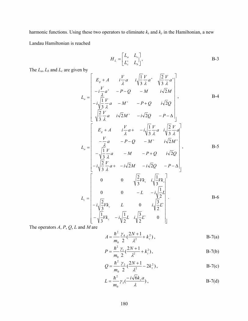
180
harmonic functions. Using these two operators to eliminate kx and ky in the Hamiltonian, a new
Landau Hamiltonian is reached
⎥⎦
⎤⎢⎣
⎡= +
bc
caL LL
LLH , B-3
The La, Lb and Lc are given by
⎥⎥⎥⎥⎥⎥⎥⎥⎥
⎦
⎤
⎢⎢⎢⎢⎢⎢⎢⎢⎢
⎣
⎡
Δ−−−
+−−−
−−−−
+
=
+
+
+
++
PQiMiaV
QiQPMaVi
MiMQPaVi
aVaViaViAE
L
g
a
2232
231
2
32
31
λ
λ
λ
λλλ
, B-4
⎥⎥⎥⎥⎥⎥⎥⎥⎥
⎦
⎤
⎢⎢⎢⎢⎢⎢⎢⎢⎢
⎣
⎡
Δ−−−−+−
+−−−
−−−−
−++
=
++
PQiMiaVi
QiQPMaV
MiMQPaV
aViaViaViAE
L
g
a
2232
231
2
32
31
λ
λ
λ
λλλ
, B-5
⎥⎥⎥⎥⎥⎥⎥⎥⎥⎥
⎦
⎤
⎢⎢⎢⎢⎢⎢⎢⎢⎢⎢
⎣
⎡
−−
−
−−=
+
+
023
21
31
230
32
2100
31
3200
LiLiVk
LiLVki
LiL
VkiVk
L
z
z
zz
c. B-6
The operators A, P, Q, L and M are
)12(2
22
4
0
2
zkNm
A ++
=λ
γh , B-7(a)
)12(2
22
1
0
2
zkNm
P ++
=λ
γh , B-7(b)
)212(2
22
2
0
2
zkNm
Q −+
=λ
γh , B-7(c)
)6(30
2
λγ
akim
L z−=h , B-7(d)

181
)3)(2
( 22
32
0
2
am
Mλ
γγ +=h . B-7(e)
The parameter γ1, γ2, γ3 and γ4 are Luttinger parameters [80] and Δ is the spin-orbit
coupling. With Landau gauge translation symmetry in the x direction is broken while translation
symmetry along the y and z directions is maintained. Therefore, ky and kz are good quantum
numbers and the envelop of the effective mass Hamiltonian HL can be written as
⎥⎥⎥⎥⎥⎥⎥⎥⎥⎥⎥
⎦
⎤
⎢⎢⎢⎢⎢⎢⎢⎢⎢⎢⎢
⎣
⎡
=
−
−
+
−
−
+
1,,8
1,,7
1,,6
,,5
,,4
,,3
2,,2
1,,1
)(
nn
nn
nn
nn
nn
nn
nn
nn
zkyki
n
aaaaaa
aa
AeF
zy
φφφφφφφφ
ν
ν
ν
ν
ν
ν
ν
ν
ν. B-8
In Eq. B-8, n is the Landau quantum number associated with the Hamiltonian matrix, ν
labels the eigenvectors, A=LxLy is the cross sectional area of the sample in the x-y plane,
)(ξφn are harmonic oscillator eigenfunctions evaluated at ykx 2λξ −= , and )(,,1 zn ka ν is complex
expansion coefficients for the νth eigenstate, which depend explicitly on n and k. Note that the
wave functions themselves will be given by the envelop functions in Eq. B-8 with each
component multiplied by the corresponding k=0 Bloch basis states given in Table 3-1.
Substituting Fnν from Eq. B-8 into the effective mass Schrodinger equation
with H given by Eq. B-3, we obtain a matrix eigenvalue equation
ννν ,,, )( nznnn FkEFH = .
That can be solved for each allowed value of the Landau quantum number, n, to obtain the
Landau levels )(, zn kE ν . The components of the normalized eigenvectors ν,nF are the expansion
coefficients ia .
182
LIST OF REFERENCES
1 T. Ando, A. B. Fowler and F. Stern, Rev. Mod. Phys. 54, 437 (1982). 2 D. A. Miller, D. S. Chemla, T. C. Damen, A. C. Gossard, W. Wiegmann, T. H. Wood,
and C. A. Burrus, Phys. Rev. B 32, 1043 (1985).
3 A. Gaj, W. Grieshaber, C. Bodin-Deshayes, J. Cibert, G. Feuillet, Y. Merle d’Aubigné, and A. Wasiela, Phys. Rev. B 50, 5512 (1994).
4 S. N. Walck and T. L. Reinecke, Phys. Rev. B 48, 17321 (1993).
5 C. Riva, F. M. Peeters, and K. Varga, Phys. Rev. B 46, 1897 (1992). 6 M. Bagnall, Y. F. Chen, Z. Zhu, T. Yao, S. Koyama, M. Y. Shen, and T. Goto, Appl.
Phys. Lett. 70, 2230 (1997). 7 Y. Chen, N. T. Tuan, Y. Segawa, H. Ko, S. Hong, and T. Yao, Appl. Phys. Lett. 78,
1469 (2001). 8 S. Cho, J. Ma, Y. Kim, Y. Sun, G. K. L. Wong, and J. B. Ketterson, Appl. Phys. Lett.
75, 2761 (1999). 9 Z.Yu, K. Wang, G. Wong, M. Kawasaki, A. Ohtomo, H. Koinuma, and Y. Segawa, J.
Cryst. Growth 184, 601 (1998). 10 L. Ley, R. A. Pollak, F. R. McFeely, S. P. Kowalczyk, and D. A. Shirley, Phys. Rev. B
9, 600 (1974). 11 P. Peyla, R. Romestain, Y. Merle d’Aubigné, G. Fishman, A. Wasiela, and H. Mariette,
Phys. Rev. B 52, 12026 (1995). 12 D. A. Kleinman, Phys. Rev. B 32, 3766 (1985). 13 D. S. Chemla, J.Y. Bigot, M.A. Mycek, S. Weiss, and W. Schäfer, Phys. Rev. Lett. 81,
2372 (1998). 14 S. L. Chuang, M. S. Luo, S. Schmitt-Rink, and A. Pinczuk, Phys. Rev. B 50, 8439
(1994). 15 R. Winkler, Phys. Rev. B 59, 15363 (1999). 16 G. E. Bauer, Phys. Rev. B 45, 9153 (1992). 17 C. Riva, F. M. Peeters, and K. Varga, Phys. Rev. B 63, 115302 (2001). 18 D. S. Citrin, Phys. Rev. B 52, 12026 (1995).

183
19 S. N. Walck, T. L. Reinecke, and P. A. Knipp, Phys. Rev. B 59, 5568 (1999). 20 R. L. Greene, K. K. Bajaj, and D. E. Phelps, Phys. Rev. B 29, 1807 (1984).
21 D. Paquet, T. M. Rice, and K. Ueda, Phys. Rev. B 32, 5208 (1985). 22 S. K. Lyo, E. D. Jones, and J. F. Klem, Phys. Rev. Lett. 61, 2265 (1988). 23 X. Zhu and S. G. Louie, Phys. Rev. B 52, 5863 (1995). 24 R. Yakovlev, V. P. Kochereshko, R. A. Suris, H. Schenk, W. Ossau, A. Waag, G.
Landwehr, P. C. Christianen, and J. C. Maan, Phys. Rev. Lett. 79, 3974 (1997). 25 H. Morf, N. d’Ambrumenil, and S. Das Sarma, Phys. Rev. B 66, 075408 (2002). 26 J. Wang, C. Sun, Y. Hashimoto, J. Kono, G. A. Khodaparast, L. Cywinski, L. J. Sham,
G. D. Sanders, C. J. Stanton, and H. Munekata, J. Phys.: Condensed Matter 18, 34754 (2006).
27 J. Wang, C. Sun, J. Kono, A. Oiwa, H. Munekata, L. Cywinski, and L. J. Sham, Phys.
Rev. Lett. 95, 167401 (2005). 28 S. A. Crooker, D. A. Tulchinsky, J. Levy, D. D. Awschalom, R. Garcia, and N.
Samarth, Phys. Rev. Lett. 75, 505 (1995). 29 S. A. Crooker, J. J. Baumberg, F. Flack, N. Samarth, and D. D. Awschalom, Phys. Rev.
Lett. 77, 2814 (1996). 30 S. A. Crooker, D. D. Awschalom, J. J. Baumberg, F. Flack, and N. Samarth, Phys. Rev.
B 56, 7574 (1997). 31 J. B. Stark, W. H. Knox, D. S. Chemla, W. Schäfer, S. Schmitt-Rink, and C. Stafford,
Phys. Rev. Lett. 65, 3033 (1990). 32 P. Kner, S. Bar-Ad, M. V. Marquezini, D. S. Chemla, and W. Schäfer, Phys. Rev. Lett.
78, 1319 (1997).
33 Y. E. Lozovik, I. V. Ovchinnikov, S. Yu. Volkov, L. V. Butov, and D. S. Chemla, Phys. Rev. B 65, 235304 (2002).
34 S. H Autler, 11C. H. Townes, Phys. Rev. 100, 703-722 (1955). 35 R. H. Dicke, Phys. Rev. 93, 99 (1954). 36 N. Skribanowitz, I. P. Herman, J. C. MacGillivray, and M. S. Feld, Phys. Rev. Lett. 30,
309 (1973).
184
37 I. Vurgaftman and J. R. Meyer, J. Appl. Phys. 89, 5815 (2001). 38 S. Schmitt, D. S. Chemla and D. A. B. Miller, Advance in Physics, 38, 89 (1989).
39 N. W.Ashcroft, Solid State Physics, Holt Rinehart and Winston, International Ed
edition, New York (1987). 40 C. Klingshrim, Semiconductor Optics, Springer, 3rd ed. Edition, New York (2006). 41 N. Peyghambarian, Introduction to Semiconductor Optics, Prentice Hall College Div.,
1st edition, New York (1993). 42 I. B. Joseph, J. M. Kuo and C. Klingshirn, Phys. Rev. Lett., 59, 1357 (1987). 43 M. S. Skolnick, P. R. Tapster and S. J. Bass, Semiconductor Science and Technology 1
29, (1986). 44 S. D. Gunapala, Appl. Phy. Lett., 58, 2024 (1991). 45 H. Temkin, T. Tanbunek and R. Logan, IEEE Photonics Technology Letters 3, 100
(1991). 46 M. Hickey, C. Damsgard and I. Farrer, Appl. Phy. Lett., 86, 252106 (2005). 47 M. Skolnick, P. Tapster and S.Bass, Semiconductor Science and Technology 1, 29
(1986). 48 R. Schneider and B. Wessels, Journal of Electronic Materials, 20, 1117 (1991).
49 T. Arakwa, Japanese Journal of Applied Physics Part 2-Letters 32, L1377 (1993). 50 P. Wiesner, R. A. Street, and H. D. Wolf, Phys. Rev. Lett. 35, 1366 (1975). 51 D. A. Miller, D. S. Chemla, T. C. Damen, A. C. Gossard, W. Wiegmann, T. H. Wood,
and C. A. Burrus, Phys. Rev. B 32, 1043 (1985).
52 M. Joffre, D. Hulin, A. Migus, and M. Combescot, Phys. Rev. Lett. 62, 74 (1989). 53 K. Leo, M. Wegener, J. Shah, D. S. Chemla, E. O. Göbel, T. C. Damen, S. Schmitt-
Rink, and W. Schäfer, Phys. Rev. Lett. 65, 1340 (1990). 54 M. Wegener, D. S. Chemla, S. Schmitt-Rink, and W. Schäfer, Phys. Rev. A 42, 5675
(1990). 55 H. J. Zeiger, J. Vidal, T. K. Cheng, E. P. Ippen, G. Dresselhaus, and M. S. Dresselhaus,
Phys. Rev. B 45, 768 (1992).

185
56 G. D. Sanders and C. J. Stanton, Phys. Rev. B 74, 205303 (2006). 57 J. L. Krause, D. H. Reitze, G. D. Sanders, A. V. Kuznetsov, and C. J. Stanton, Phys.
Rev. B 57, 9024 (1998). 58 A. V. Kuznetsov and C. J. Stanton, Phys. Rev. B 48, 10828 (1993). 59 G. N. Ostojic, J. Shaver, S. Zaric, and J. Kono, Physica E-Low-Dimensional Systems &
Nanostructures 29, 469 (2005). 60 S. Zaric, G. Ostojic, J. Shaver, and J. Kono, Phys. Rev. Lett., 96, 016406 (2006).
61 S. Zaric, G. N. Ostojic, J. Kono , J. Shaver, V. C. Moore, M. S. Strano, R. H. Hauge, R.
E. Smalley, and X. Wei, Science 304, 1129 (2004). 62 J. Schnack, M. Bruger, M. Luban, P. Kogerler, E. Morosan, R. Fuchs, R. Modler, J.
Musfeldt, and X. Wei, Phys. Rev. B 73, 094401 (2006).
63 J. Woodward, J. Choi, and J. Musfeldt, Phys. Rev. B 71,174416 (2005). 64 J. Cao, J. Haraldsen, R. Rai, S. Brown, J. Musfeldt, Y. Wang, and X. Wei, Phys. Rev. B
74, 045113 (2006). 65 R. Rai, J. Cao, J. Musfeldt, S. Kim, and X. Wei, Phys. Rev. B 75, 184414 (2007).
66 R. Rai, J. Cao, J. Musfeldt, and X. Wei, Phys. Rev. B 73, 075112 (2006).
67 L. Kuskovsky, W. MacDonald, A. O. Govorov, L. Mourokh, and X. Wei, Phys. Rev. B
76, 035342 (2007).
68 M. Guillot, F. Zhang, Y. Xu, J. Yang, and X.,Wei, J. Appl. Phys. 101, C510 (2007). 69 DC Field Instruments & Tools at the National High Magnetic Field Laboratory,
1http://www.magnet.fsu.edu/usershub/scientificdivisions/dcfield/cell5grad/cell5side-grad.html, last accessed September, 2007.
70 A. Crubellier, S. Liberman, and P. Pillet, Phys. Rev. Lett. 41, 1237 (1978). 71 G. Basterd, Wavemechanics Applied to Semiconductor Heterostructures, Wiley-
Interscience, 1st edition, NewYork (1991). 72 E.O. Kane, J. Phys. Chem. Solids 1, 249(1957). 73 D. W. Kim, Y. A. Leem, S. D. Yoo, D. H. Woo, D. H. Lee, and J. C. Woo, Phys. Rev.
B.47, 2042 (1993).
186
74 G. Bastard, E. E. Mendez, L. L. Chang, and L. Esaki, Phys. Rev. B, 26 1974 (1982). 75 L Greene, K. Krishan, and P. Dwight, Phys. Rev. B 29, 1807 (1984).
76 D. A. Miller, D. S. Chemla, T. C. Damen, A. C. Gossard, W. Wiegmann, T. H. Wood,
and C. A. Burrus, Phys. Rev. B 32, 1043 (1985). 77 A. Baldereschi and C. Nunzio, Phys. Rev. B 3, 439 (1971). 78 Ioffe Institute, Electronic archive New Semiconductor Materials. Characteristics and
Properties, GaAs 1http://www.ioffe.rssi.ru/SVA/NSM/Semicond/GaAs/Figs/421.gif, last accessed September, 2007.
79 Ioffe Institute, Electronic archive New Semiconductor Materials. Characteristics and Properties, GaN, 1http://www.ioffe.rssi.ru/SVA/NSM/Semicond/GaN/bandstr.html, last accessed September, 2007.
80 G. E. Bauer and T. Ando, Phys. Rev. B 38, 6015 (1988). 81 I. Vurgaftmana and J. R. Meyer, J. of Appl. Phys., 89, 5815 (2001). 82 Y. D. Jho, F. Kyrychenko, G. Sanders, X. Wei, D. Reitze, J.Kono, C. Stanton, and S.
Solomon, Phys. Rev. B 72, 045340 (2005). 83 L. V. Butov, A. Zrenner, M. Shayegan, G. Abstreiter, and H. C. Manoharan, Phys. Rev.
B 49, 14054 (1994). 84 L. V. Butov, V. D. Kulakovskii, G. E. Bauer, A. Forchel, and D. Grützmacher, Phys.
Rev. B 46, 12765 (1992). 85 G. E. Bauer and T. Ando, Phys. Rev. B 37, 3130 (1988), H. Aoki and T. Ando, Phys.
Rev. Lett. 54, 831 (1985). 86 L. V. Butov, V. D. Egorov, V. D. Kulakovskii, and T. G. Andersson, Phys. Rev. B 46,
15156 (1992). 87 A. H. MacDonald and D. S. Ritchie, Phys. Rev. B 33, 8336 (1986). 88 L. V. Butov, V. D. Kulakovskii, E. Lach, A. Forchel, and D. Grützmacher, Phys. Rev.
B 44, 10680 (1991). 89 L. V. Butov, V. D. Kulakovskii, and G. E. Bauer, Phys. Rev. B 46, 12765 (1992). 90 G. E. Bauer and T. Ando, Phys. Rev. B 37, 3130 (1988). 91 W. Hanke and L. J. Sham Phys. Rev. Lett. 43, 387 (1979).

187
92 S. R. Yang and L. J. Sham Phys. Rev. Lett. 58, 2598 (1987). 93 L. V. Butov, V. D. Kulakovskii, and T. G. Andersson, Phys. Rev. B 44, 1692 (1991).
94 R. Pidgeon and R. N. Brown, Phys. Rev. 146, 575 (1966); E. O. Kane J. Phys. Chem.
Solids 1, 249 (1957). 95 L. V. Butov, V. D. Kulakovskii, and G. E. Bauer, Phys. Rev. B 46, 12765 (1992). 96 R. Boyd, Nonlinear Optics, Academic Press, 2nd edition, New York (2002). 97 Y. Yoshihisa, Mesoscopic Quantum Optics, John Wiley, 3rd edition, New York (1999). 98 P. Meystre, Atomic Optics, Springer-Verlag, 2nd edition, New York (2001). 99 L. Allen et al., Optical Resonance and Two-level Atoms, Wiley, 2nd edition, New York
(1975). 100 F. Tsai et al., Journal of Applied Physics 89, 7875 (2007). 101 A. Djurisic, W. Kwok, Y. Leung, et al. , Nanotechnology 17,244 ( 2006). 102 H. M. Gibbs, Q. H. Vrehen, and H. M. Hikspoors, Phys. Rev. Lett. 39, 547 (1977). 103 N. Skribanowitz, I. P. Herman, J. C. MacGillivray, and M. S. Feld, Phys. Rev. Lett. 30,
309 (1973). 104 M. Gross, C. Fabre, P. Pillet, and S. Haroche, Phys. Rev. Lett. 36, 1035 (1976). 105 Y. Kaluzny, P. Goy, M. Gross, J. M. Raimond, and S. Haroche, Phys. Rev. Lett. 51,
1175 (1983). 106 A. T. Rosenberger and T. A. DeTemple, Phys. Rev. A 24, 868 (1981). 107 R. Bonifacio, P. Schwendimann, and Fritz Haake, Phys. Rev. A 4, 854 (1971); R.
Bonifacio, P. Schwendimann, and F. Haake, Phys. Rev. A 4, 302 (1971). 108 J. C. MacGillivray and M. S. Feld, Phys. Rev. A 14, 1169 (1976). 109 H. M. Gibbs, Q. H. Vrehen, and H. M. Hikspoors, Phys. Rev. Lett. 39, 547 (1977). 110 A. Crubellier, S. Liberman, and P. Pillet, Phys. Rev. Lett. 41, 1237 (1978). 111 A. Belyanin, V.Kocharovsky and V.Kocharovsky, Quantum and Semiclass. Optics, 9, 1
(1997).

188
112 A. Kazantzev and V. Smirnov, Sov. Phys. JETP. 19, 130 (1964); A. Alekseev, Y.Vdovin, and V. Galitzky, Sov. Phys. JETP. 19, 220, (1964).
113 V. Zheleznyakov and V. Kocharovsky, Sov. Phys.Usp, 32, 835 (1989). 114 A. Belyanin, V.V. Kocharovsky, and Vl.V. Kocharovsky, JEOS Part B (Quantum &
Semiclass. Optics) 10, L13 (1998). 115 A. Belyanin, V.V. Kocharovsky, and Vl.V. Kocharovsky, Bull. Russian Acad.
Sciences, 62, 372 (1998). 116 A. Belyanin, V.V. Kocharovsky, and Vl.V. Kocharovsky, Computers Math.
Application. 34, 845 (1997). 117 A. Belyanin, V.V. Kocharovsky, and Vl.V. Kocharovsky, Laser Physics, 5, 1121
(1995). 118 A. Belyanin, V.V. Kocharovsky, and Vl.V. Kocharovsky, Solid State Commun., 80,
243 (1991). 119 A. I. Lvovsky, S. R. Hartmann, and F. Moshary, Phys. Rev. Lett. 82, 4420 (1999). 120 Spontaneous emission, Wikipedia, the free encyclopedia,
1http://en.wikipedia.org/wiki/Spontaneous_emission, last accessed September, 2007. 121 Stimulated emission, Wikipedia, the free encyclopedia,
1http://en.wikipedia.org/wiki/Stimulated_emission, last accessed September, 2007. 122 Z. Z. Ye et al., Appl. Phys. Lett. 91, 113503 (2007).
123 Y. Ogawa and S. Fujihara, J. Electrochem. Soc. 154, J283 (2007).
124 D. Yu, Y. Chen, B. Li, and S. Ren, Appl. Phys. Lett. 91, 091116 (2007). 125 F. A. Selim, M. H. Weber, D. Solodovnikov, and K. G. Lynn, Phys. Rev. Lett. 99,
085502 (2007). 126 M. Al-Suleiman, A. El-Shaer, A. Bakin, H.H. Wehmann, and A. Waag, Appl. Phys.
Lett. 91, 081911 (2007). 127 B. Monemar, Phys. Rev. B 10, 676 (1974). 128 W. F. Brinkman and T. M. Rice, Phys. Rev. B 7, 1508 (1973). 129 Y. Harada and S. Hashimoto, Phys. Rev. B 68, 045421 (2003); M. Zamfirescu, A.
Kavokin, B. Gil, G. Malpuech, and M. Kaliteevski, Phys. Rev. B 65, 161205 (2002).

189
130 Ü. Özgür,a Ya. I. Alivov, C. Liu, A. Teke,b M. A. Reshchikov, S. Doğan,c V. Avrutin,S.-J. Cho, and H. Morkoçd, J. of Appl. Phys. 98, 041301 (2005).
131 X. Sun , K. Maeda, M. Faucheur M, et al., Applied Catalysis A-General 327, 114
(2007). 132 A. Kobayashi, S. Kawano, Y. Kawaguchi, et al., Appl. Phys. Lett. 90, 041908 (2007). 133 C. Sun, S. Sun, K. Lin, et al., Appl. Phys. Lett. 87, 023106 (2005). 134 S. Yamamoto, H. Yano, T. Mishina, et al., J. of Lumin., 126, 257 ( 2007). 135 Y. S. Park, C. W. Litton, T. C. Collins, and D. C. Reynolds, Phys. Rev. 143, 512
(1966). 136 A. Rodina, M .Strassburg, M. Dworzak, et al., Phys. Rev. B 69 (12), (2005). 137 R. Dietz, D. Thomas, and J. Hopfield, J. of Appl. Phys. 32: 2282& Suppl. (1961). 138 D. C. Reynolds, D. C. Look, B. Jogai, C. W. Litton, T. C. Collins, W. Harsch, and G.
Cantwel, Phys. Rev. B 57, 12151 (1998). 139 D. Reynolds, D. Look, B. Jogai, et al., J. of Appl. Phys. 86, 5598 (1999).
140 D. C. Reynolds, D. C. Look, B. Jogai, C. W. Litton, T. C. Collins, W. Harsch, and G.
Cantwell, Phys. Rev. B 57, 12151 (1998). 141 Chris Cook and Chris Stanton, in preparation for PRB. 142 A. Teke, U. Ozgur, S. Dogan, et al., Phys. Rev. B 70, 195207 (2004). 143 J. Shah, Ultrafast Spectroscopy of Semiconductors and Semiconductor Nanostructures,
Springer, 2nd enlarged Edition, New York (1999). 144 L. Pavesi, J. Appl. Phys. 80, 216 (1996). 145 I. Mihalcescu, J. C. Vial, and R. Romestain, Phys. Rev. Lett. 80, 3392 (1998). 146 I. Mihalcescu, J. C. Vial, and R. Romestain, J. Appl. Phys. 80, 2404 (1996). 147 E. Martin, C. Delerue, G. Allan, and M. Lannoo, Phys. Rev. B 50, 18 258 (1994).

190
BIOGRAPHICAL SKETCH
Xiaoming Wang was born in Nov. 1971. He earned the Bachelor of Science degree at
Tianjin University, China, in 1994. After that he entered the graduate school of Tianjin
University and got his Master of Science degree in physics in 1997. Right after that, he started
his job as a research associate in the Institute of Physics, China Academy of Sciences. After three
year of being a research associate in the Institute of Physics, Chinese Sciences, he resigned his
job and came to University of Florida in 2000, to pursue a Ph.D in physics. He joined Prof.
David Reitze’s ultrafast group in summer 2001. He has been working for several different
research projects, some of which are related to this dissertation.


![Ultrafast spectroscopic investigation of a fullerene poly ... · the fullerene derivative PCB ([6,6]-phenyl-C 61-butyric acid ester), adapted from PCBM. The fluorescence of the P3HT](https://img.dokumen.tips/doc/110x75/5f414403ccd47957c63bba3c/ultrafast-spectroscopic-investigation-of-a-fullerene-poly-the-fullerene-derivative.jpg)