Embed Size (px)
Citation preview

Ultra Low Noise, Medium Current
E-PHEMT
NotesA. Performance and quality attributes and conditions not expressly stated in this specification document are intended to be excluded and do not form a part of this specification document. B. Electrical specifications and performance data contained in this specification document are based on Mini-Circuit’s applicable established test performance criteria and measurement instructions. C. The parts covered by this specification document are subject to Mini-Circuits standard limited warranty and terms and conditions (collectively, “Standard Terms”); Purchasers of this part are entitled to the rights and benefits contained therein. For a full statement of the Standard Terms and the exclusive rights and remedies thereunder, please visit Mini-Circuits’ website at www.minicircuits.com/MCLStore/terms.jsp
Mini-Circuits®
www.minicircuits.com P.O. Box 350166, Brooklyn, NY 11235-0003 (718) 934-4500 [email protected] Page 1 of 13
SAV-541+
REV. DM151107ED-13377SAV-541+1509
0.45-6GHz
CASE STYLE: MMM1362
Product Features• Low Noise Figure, 0.5 dB• Gain, 17 dB at 2 GHz• High Output IP3, +33 dBm• Output Power at 1dB comp., +20 dBm • High Current, 60mA• Wide bandwidth• External biasing and matching required• May be used as replacement a,b for Avago ATF-54143
Typical Applications• Cellular• ISM• GSM• WCDMA• WiMax• WLAN• UNII and HIPERLAN
Function Pin Number DescriptionSource 2 & 4 Source terminal, normally connected to ground
Gate 3 Gate used for RF input
Drain 1 Drain used for RF output
General DescriptionSAV-541+ is an ultra-low noise, high IP3 transistor device, manufactured using E-PHEMT* technology enabling it to work with a single positive supply voltage. It has outstanding Noise Figure, particularly be-low 2.5 GHz, and when combining this noise figure with high IP3 performance in a single device it makes it an ideal amplifier for demanding base station applications. We offer these units assembled into a com-plete module, 50Ω in/out, noise matched and fully specified. For more information please see our TAMP family of models on our web site.
simplified schematic and pin description
G AT E
S OUR C E
DR AINDR AIN 1
3 G AT E
4 S OUR C E
S OUR C E 2
SOT-343 (SC-70) PACKAGE
* Enhancement mode Pseudomorphic High Electron Mobility Transistor.
a. Suitability for model replacement within a particular system must be determined by and is solely the responsibility of the customer based on, among other things, electrical perfor-mance criteria, stimulus conditions, application, compatibility with other components and environmental conditions and stresses.b. The Avago ATF-54143 part number is used for identification and comparison purposes only.
+RoHS CompliantThe +Suffix identifies RoHS Compliance. See our web site for RoHS Compliance methodologies and qualifications

E-PHEMT SAV-541+
NotesA. Performance and quality attributes and conditions not expressly stated in this specification document are intended to be excluded and do not form a part of this specification document. B. Electrical specifications and performance data contained in this specification document are based on Mini-Circuit’s applicable established test performance criteria and measurement instructions. C. The parts covered by this specification document are subject to Mini-Circuits standard limited warranty and terms and conditions (collectively, “Standard Terms”); Purchasers of this part are entitled to the rights and benefits contained therein. For a full statement of the Standard Terms and the exclusive rights and remedies thereunder, please visit Mini-Circuits’ website at www.minicircuits.com/MCLStore/terms.jsp
Mini-Circuits®
www.minicircuits.com P.O. Box 350166, Brooklyn, NY 11235-0003 (718) 934-4500 [email protected] Page 2 of 13
Symbol Parameter Condition Min. Typ. Max. UnitsDC Specifications
VGS Operational Gate Voltage VDS=3V, IDS=60 mA 0.37 0.48 0.69 V
VTH Threshold Voltage VDS=3V, IDS=4 mA 0.18 0.26 0.38 V
IDSS Saturated Drain Current VDS=3V, VGS=0 V 1.0 5.0 µA
GM Transconductance
VDS=3V, Gm=∆ IDS/∆VGS ∆VGS=VGS1-VGS2
VGS1=VGS at IDS=60 mAVGS2=VGS1+0.05V
——
230——
——
392——
——
560——
mS
IGSS Gate leakage Current VGD=VGS=-3V 200 µA
RF Specifications, Z0=50 Ohms (Figure 1)
NF(1) Noise Figure VDS=3V, IDS=60 mA f=0.9 GHz 0.4 —
dB
f=2.0 GHz 0.5 0.9f=3.9 GHz 1.0 —f=5.8 GHz 1.9 —
VDS=4V, IDS=60 mA f=2.0 GHz 0.5 —
Gain Gain
VDS=3V, IDS=60 mA f=0.9 GHz — 23.2 —
dB
f=2.0 GHz 15.0 17.6 18.5f=3.9 GHz — 12.5 —f=5.8 GHz — 8.7 —
VDS=4V, IDS=60 mA f=2.0 GHz — 17.4 —
OIP3 Output IP3
VDS=3V, IDS=60 mA f=0.9 GHz — 32.6
dBm
f=2.0 GHz 30.0 33.1f=3.9 GHz — 33.0f=5.8 GHz — 31.0
VDS=4V, IDS=60 mA f=2.0 GHz 35.1
P1dB(2) Power output at 1 dB Compression
VDS=3V, IDS=60 mA f=0.9 GHz 19.1
dBm
f=2.0 GHz 19.2f=3.9 GHz 19.0f=5.8 GHz 18.2
VDS=4V, IDS=60 mA f=2.0 GHz 21.5
Notes:(1) Includes test board loss (tested on Mini-Circuits TB-471+ test board)(2) Drain current was allowed to increase during compression measurements.(3) Operation of this device above any one of these parameters may cause permanent damage.(4) Assumes DC quiescent conditions.(5) IGS is limited to 2 mA during test.
Absolute Maximum Ratings(3) Symbol Parameter Max. Units
VDS(4) Drain-Source Voltage 5 V
VGS(4) Gate-Source Voltage -5 to 0.7 V
VGD(4) Gate-Drain Voltage -5 to 0.7 V
IDS(4) Drain Current 120 mA
IGS Gate Current 2 mAPDISS Total Dissipated Power 360 mWPIN
(5) RF Input Power 17 dBmTCH Channel Temperature 150 °CTOP Operating Temperature -40 to 85 °CTSTD Storage Temperature -65 to 150 °CΘJC Thermal Resistance 160 °C/W
Electrical Specifications at TAMB=25°C, Frequency 0.45 to 6 GHz
E-PHEMT SAV-541+
NotesA. Performance and quality attributes and conditions not expressly stated in this specification document are intended to be excluded and do not form a part of this specification document. B. Electrical specifications and performance data contained in this specification document are based on Mini-Circuit’s applicable established test performance criteria and measurement instructions. C. The parts covered by this specification document are subject to Mini-Circuits standard limited warranty and terms and conditions (collectively, “Standard Terms”); Purchasers of this part are entitled to the rights and benefits contained therein. For a full statement of the Standard Terms and the exclusive rights and remedies thereunder, please visit Mini-Circuits’ website at www.minicircuits.com/MCLStore/terms.jsp
Mini-Circuits®
www.minicircuits.com P.O. Box 350166, Brooklyn, NY 11235-0003 (718) 934-4500 [email protected] Page 3 of 13
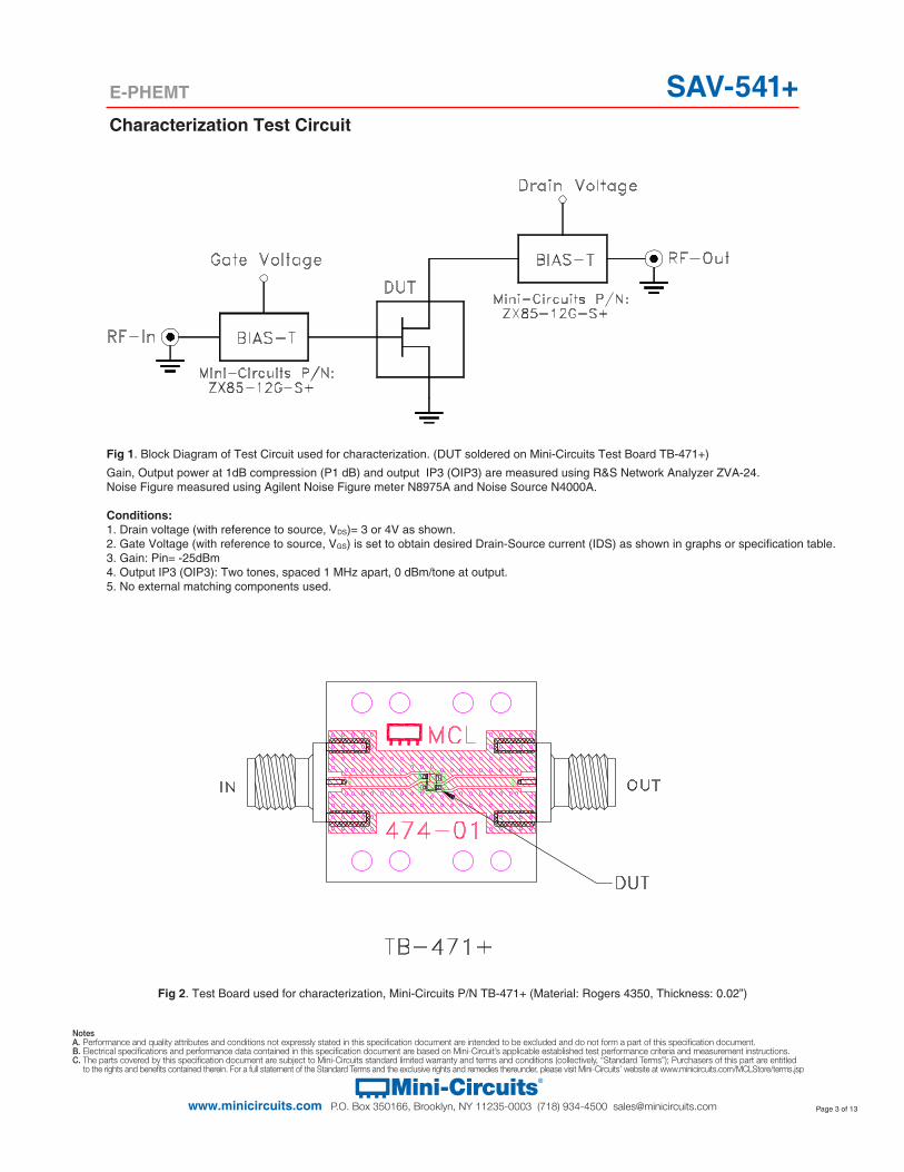
Fig 1. Block Diagram of Test Circuit used for characterization. (DUT soldered on Mini-Circuits Test Board TB-471+)
Gain, Output power at 1dB compression (P1 dB) and output IP3 (OIP3) are measured using R&S Network Analyzer ZVA-24.Noise Figure measured using Agilent Noise Figure meter N8975A and Noise Source N4000A.
Conditions:1. Drain voltage (with reference to source, VDS)= 3 or 4V as shown.2. Gate Voltage (with reference to source, VGS) is set to obtain desired Drain-Source current (IDS) as shown in graphs or specification table.3. Gain: Pin= -25dBm4. Output IP3 (OIP3): Two tones, spaced 1 MHz apart, 0 dBm/tone at output.5. No external matching components used.
Fig 2. Test Board used for characterization, Mini-Circuits P/N TB-471+ (Material: Rogers 4350, Thickness: 0.02”)
Characterization Test Circuit

E-PHEMT SAV-541+
NotesA. Performance and quality attributes and conditions not expressly stated in this specification document are intended to be excluded and do not form a part of this specification document. B. Electrical specifications and performance data contained in this specification document are based on Mini-Circuit’s applicable established test performance criteria and measurement instructions. C. The parts covered by this specification document are subject to Mini-Circuits standard limited warranty and terms and conditions (collectively, “Standard Terms”); Purchasers of this part are entitled to the rights and benefits contained therein. For a full statement of the Standard Terms and the exclusive rights and remedies thereunder, please visit Mini-Circuits’ website at www.minicircuits.com/MCLStore/terms.jsp
Mini-Circuits®
www.minicircuits.com P.O. Box 350166, Brooklyn, NY 11235-0003 (718) 934-4500 [email protected] Page 4 of 13
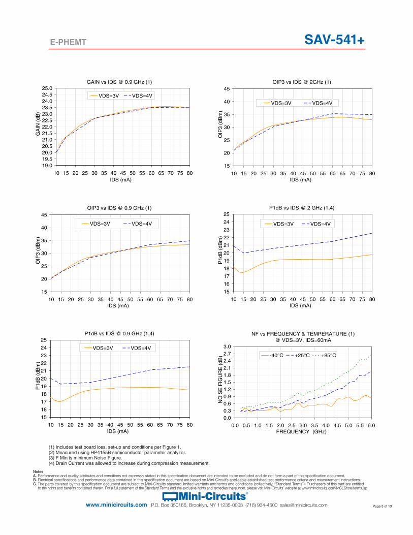
Typical Performance Curves
I-V (VGS=0.1V PER STEP) (2)
0
20
40
60
80
100
120
0.0 0.5 1.0 1.5 2.0 2.5 3.0 3.5 4.0 4.5 5.0 5.5 6.0VDS (V)
IDS
(mA
)
0.2V
0.3V
0.4V
0.5V
0.6V
0.7V
NOISE FIGURE vs IDS @ 0.9 GHz (1)
0.1
0.2
0.3
0.4
0.5
0.6
0.7
0.8
10 15 20 25 30 35 40 45 50 55 60 65 70 75 80IDS (mA)
NO
ISE
FIG
UR
E (
dB) VDS=3V VDS=4V
F Min vs IDS @ 2 GHz (3)
0.25
0.27
0.29
0.31
0.33
0.35
0.37
0.39
0.41
0.43
0.45
10 15 20 25 30 35 40 45 50 55 60 65 70 75 80IDS (mA)
F M
IN (
dB)
VDS=2V VDS=3V VDS=4V
GAIN vs IDS @ 2 GHz (1)
14.014.515.015.516.016.517.017.518.018.519.019.520.0
10 15 20 25 30 35 40 45 50 55 60 65 70 75 80IDS (mA)
GA
IN (
dB)
VDS=3V VDS=4V
F Min vs IDS @ 0.9 GHz (3)
0.10
0.11
0.12
0.13
0.14
0.15
0.16
0.17
0.18
0.19
0.20
10 15 20 25 30 35 40 45 50 55 60 65 70 75 80IDS (mA)
F M
IN (
dB)
VDS=2V VDS=3V VDS=4V
NOISE FIGURE vs IDS @ 2 GHz (1)
0.1
0.2
0.3
0.4
0.5
0.6
0.7
0.8
10 15 20 25 30 35 40 45 50 55 60 65 70 75 80IDS (mA)
NO
ISE
FIG
UR
E(d
B)
VDS=3V VDS=4V
(1) Includes test board loss, set-up and conditions per Figure 1.(2) Measured using HP4155B semiconductor parameter analyzer.(3) F Min is minimum Noise Figure.(4) Drain Current was allowed to increase during compression measurement.
E-PHEMT SAV-541+
NotesA. Performance and quality attributes and conditions not expressly stated in this specification document are intended to be excluded and do not form a part of this specification document. B. Electrical specifications and performance data contained in this specification document are based on Mini-Circuit’s applicable established test performance criteria and measurement instructions. C. The parts covered by this specification document are subject to Mini-Circuits standard limited warranty and terms and conditions (collectively, “Standard Terms”); Purchasers of this part are entitled to the rights and benefits contained therein. For a full statement of the Standard Terms and the exclusive rights and remedies thereunder, please visit Mini-Circuits’ website at www.minicircuits.com/MCLStore/terms.jsp
Mini-Circuits®
www.minicircuits.com P.O. Box 350166, Brooklyn, NY 11235-0003 (718) 934-4500 [email protected] Page 5 of 13
(1) Includes test board loss, set-up and conditions per Figure 1.(2) Measured using HP4155B semiconductor parameter analyzer.(3) F Min is minimum Noise Figure.(4) Drain Current was allowed to increase during compression measurement.
GAIN vs IDS @ 0.9 GHz (1)
19.019.520.020.521.021.522.022.523.023.524.024.525.0
10 15 20 25 30 35 40 45 50 55 60 65 70 75 80IDS (mA)
GA
IN (
dB)
VDS=3V VDS=4V
P1dB vs IDS @ 2 GHz (1,4)
15
16
17
18
19
20
21
22
23
24
25
10 15 20 25 30 35 40 45 50 55 60 65 70 75 80IDS (mA)
P1d
B (
dBm
)VDS=3V VDS=4V
P1dB vs IDS @ 0.9 GHz (1,4)
15
16
17
18
19
20
21
22
23
24
25
10 15 20 25 30 35 40 45 50 55 60 65 70 75 80IDS (mA)
P1d
B (
dBm
)
VDS=3V VDS=4V
NF vs FREQUENCY & TEMPERATURE (1)@ VDS=3V, IDS=60mA
0.00.30.60.91.21.51.82.12.42.73.0
0.0 0.5 1.0 1.5 2.0 2.5 3.0 3.5 4.0 4.5 5.0 5.5 6.0FREQUENCY (GHz)
NO
ISE
FIG
UR
E (
dB) -40°C +25°C +85°C
OIP3 vs IDS @ 0.9 GHz (1)
15
20
25
30
35
40
45
10 15 20 25 30 35 40 45 50 55 60 65 70 75 80IDS (mA)
OIP
3 (d
Bm
)
VDS=3V VDS=4V
OIP3 vs IDS @ 2GHz (1)
15
20
25
30
35
40
45
10 15 20 25 30 35 40 45 50 55 60 65 70 75 80IDS (mA)
OIP
3 (d
Bm
)
VDS=3V VDS=4V
E-PHEMT SAV-541+
NotesA. Performance and quality attributes and conditions not expressly stated in this specification document are intended to be excluded and do not form a part of this specification document. B. Electrical specifications and performance data contained in this specification document are based on Mini-Circuit’s applicable established test performance criteria and measurement instructions. C. The parts covered by this specification document are subject to Mini-Circuits standard limited warranty and terms and conditions (collectively, “Standard Terms”); Purchasers of this part are entitled to the rights and benefits contained therein. For a full statement of the Standard Terms and the exclusive rights and remedies thereunder, please visit Mini-Circuits’ website at www.minicircuits.com/MCLStore/terms.jsp
Mini-Circuits®
www.minicircuits.com P.O. Box 350166, Brooklyn, NY 11235-0003 (718) 934-4500 [email protected] Page 6 of 13
GAIN vs FREQUENCY & TEMPERATURE (1)@ VDS=3V, IDS=60mA
258
1114172023262932
0.0 0.5 1.0 1.5 2.0 2.5 3.0 3.5 4.0 4.5 5.0 5.5 6.0FREQUENCY (GHz)
GA
IN (
dB)
-45°C +25°C +85°C
NF vs FREQUENCY & TEMPERATURE (1)@ VDS=4V, IDS=60mA
0.00.30.60.91.21.51.82.12.42.73.0
0.0 0.5 1.0 1.5 2.0 2.5 3.0 3.5 4.0 4.5 5.0 5.5 6.0FREQUENCY (GHz)
NO
ISE
FIG
UR
E (
dB) -40°C +25°C +85°C
GAIN vs FREQUENCY & TEMPERATURE (1)@ VDS=4V, IDS=60mA
258
1114172023262932
0.0 0.5 1.0 1.5 2.0 2.5 3.0 3.5 4.0 4.5 5.0 5.5 6.0FREQUENCY (GHz)
GA
IN (
dB)
-45°C +25°C +85°C
OIP3 vs FREQUENCY & TEMPERATURE (1)@ VDS=4V, IDS=60mA
2527293133353739414345
0.0 0.5 1.0 1.5 2.0 2.5 3.0 3.5 4.0 4.5 5.0 5.5 6.0FREQUENCY (GHz)
OIP
3 (d
Bm
)
-45°C +25°C +85°C
P1dB vs FREQUENCY & TEMPERATURE (1,4)@ VDS=3V, IDS=60mA
1617171818192020212122
0.0 0.5 1.0 1.5 2.0 2.5 3.0 3.5 4.0 4.5 5.0 5.5 6.0FREQUENCY (GHz)
P1d
B (
dBm
)
-45°C +25°C +85°C
OIP3 vs FREQUENCY & TEMPERATURE (1)@ VDS=3V, IDS=60mA
2527293133353739414345
0.0 0.5 1.0 1.5 2.0 2.5 3.0 3.5 4.0 4.5 5.0 5.5 6.0FREQUENCY (GHz)
OIP
3 (d
Bm
)
-45°C +25°C +85°C
(1) Includes test board loss, set-up and conditions per Figure 1.(2) Measured using HP4155B semiconductor parameter analyzer.(3) F Min is minimum Noise Figure.(4) Drain Current was allowed to increase during compression measurement.
E-PHEMT SAV-541+
NotesA. Performance and quality attributes and conditions not expressly stated in this specification document are intended to be excluded and do not form a part of this specification document. B. Electrical specifications and performance data contained in this specification document are based on Mini-Circuit’s applicable established test performance criteria and measurement instructions. C. The parts covered by this specification document are subject to Mini-Circuits standard limited warranty and terms and conditions (collectively, “Standard Terms”); Purchasers of this part are entitled to the rights and benefits contained therein. For a full statement of the Standard Terms and the exclusive rights and remedies thereunder, please visit Mini-Circuits’ website at www.minicircuits.com/MCLStore/terms.jsp
Mini-Circuits®
www.minicircuits.com P.O. Box 350166, Brooklyn, NY 11235-0003 (718) 934-4500 [email protected] Page 7 of 13
P1dB vs FREQUENCY & TEMPERATURE (1,4)@ VDS=4V, IDS=60mA
1819192021222223242425
0.0 0.5 1.0 1.5 2.0 2.5 3.0 3.5 4.0 4.5 5.0 5.5 6.0FREQUENCY (GHz)
P1d
B (
dBm
)
-45°C +25°C +85°C
F Min vs FREQ @ VDS=3V (3)
0.0
0.2
0.4
0.6
0.8
1.0
1.2
1.4
0.0 0.5 1.0 1.5 2.0 2.5 3.0 3.5 4.0 4.5 5.0 5.5 6.0FREQUENCY (GHz)
F M
IN (
dB)
40 mA 60 mA 80 mA
Notes:Noise parameters were measured over 0.5 to 6 GHz by Modelithics® using a solid state tuner-based noise parameter (NP) test system available from Maury Microwave. F Min, optimimum source reflection coefficient and noise resistance values are calculated values based on a set of measurements made at approximately 16 different impedances. Some data smoothing was applied to ar-rive at the presented data set.
S-parameters were measured by Modelithics® on an Anritsu Lightning vector network analyzer over 0.1 to 18GHz using 350um pitch RF probes from GGB industries combined with customized thru-reflect-line (TRL) calibration standards. The reference plane is at the device package leads, as shown in the picture.
Fig 3. Reference Plane Location
Reference Plane Location for S and Noise Parameters (see data in pages 8-11)(Refer to Application Note AN-60-040)
(1) Includes test board loss, set-up and conditions per Figure 1.(2) Measured using HP4155B semiconductor parameter analyzer.(3) F Min is minimum Noise Figure.(4) Drain Current was allowed to increase during compression measurement.

E-PHEMT SAV-541+
NotesA. Performance and quality attributes and conditions not expressly stated in this specification document are intended to be excluded and do not form a part of this specification document. B. Electrical specifications and performance data contained in this specification document are based on Mini-Circuit’s applicable established test performance criteria and measurement instructions. C. The parts covered by this specification document are subject to Mini-Circuits standard limited warranty and terms and conditions (collectively, “Standard Terms”); Purchasers of this part are entitled to the rights and benefits contained therein. For a full statement of the Standard Terms and the exclusive rights and remedies thereunder, please visit Mini-Circuits’ website at www.minicircuits.com/MCLStore/terms.jsp
Mini-Circuits®
www.minicircuits.com P.O. Box 350166, Brooklyn, NY 11235-0003 (718) 934-4500 [email protected] Page 8 of 13
MAXIMUM STABLE GAIN (MSG)/MAXIMUM AVAILABLE GAIN (MAG) vs. FREQUENCY
-15
-10
-5
0
5
10
15
20
25
30
35
40
0 5 10 15 20Frequency (GHz)
MS
G/M
AG
and
S21
(dB
)
MSG/MAGS21(dB)
Freq.(GHz)
S11 S21 S12 S22MSG/MAG
(dB)Mag. Ang. Mag.Mag (dB) Ang. Mag. Ang. Mag. Ang.
Typical S-parameters, VDS=3V and IDS=40 mA (Fig. 3)
Typical Noise Parameters, VDS=3V and IDS=40 mA (Fig. 3)
Freq.(GHz)
F Min.(dB)
GOpt(Magnitude)
GOpt(Angle) Rn/50
GaAssociatedGain (dB)
0.5 0.071 0.34 27.00 0.05 27.9 0.7 0.101 0.35 37.65 0.05 25.7 0.9 0.131 0.35 48.14 0.04 23.9 1.0 0.146 0.36 53.32 0.04 23.2 1.9 0.281 0.39 98.07 0.03 18.3 2.0 0.296 0.39 102.83 0.03 17.9 2.4 0.356 0.40 121.48 0.03 16.6 3.0 0.446 0.42 148.20 0.03 15.0 3.9 0.581 0.45 -174.52 0.05 13.4 5.0 0.747 0.48 -133.51 0.10 11.9 5.8 0.867 0.50 -106.84 0.14 10.9 6.0 0.897 0.50 -100.59 0.15 10.6
0.1 0.99 -16.6 25.3 28.1 169.5 0.008 89.1 0.55 -14.7 34.8 0.5 0.86 -74.6 19.6 25.8 132.2 0.035 54.4 0.43 -55.3 27.5 0.9 0.75 -112.6 14.2 23.0 109.0 0.047 40.5 0.32 -83.3 24.8 1.0 0.74 -120.4 13.2 22.4 104.6 0.049 38.4 0.30 -89.5 24.3 1.5 0.68 -149.6 9.5 19.6 86.7 0.057 31.3 0.23 -114.1 22.3 1.9 0.66 -166.7 7.7 17.8 75.4 0.062 27.5 0.19 -131.2 21.0 2.0 0.66 -170.5 7.4 17.4 72.9 0.063 26.6 0.19 -135.2 20.7 2.5 0.65 172.8 6.0 15.6 61.0 0.07 22.9 0.17 -153.9 19.3 3.0 0.65 158.7 5.0 14.1 50.2 0.077 19.5 0.16 -171.3 18.2 4.0 0.66 134.4 3.8 11.6 30.0 0.091 11.9 0.16 156.7 15.8 5.0 0.68 113.5 3.0 9.7 11.1 0.104 2.7 0.18 130.5 13.3 6.0 0.71 94.7 2.5 8.0 -7.1 0.118 -7.5 0.22 109.1 11.7 7.0 0.75 77.8 2.1 6.4 -24.7 0.13 -18.3 0.28 90.7 10.5 8.0 0.78 62.4 1.8 5.0 -41.5 0.14 -29.4 0.33 74.8 9.6 9.0 0.82 47.8 1.5 3.6 -57.8 0.146 -41.0 0.40 60.0 9.0 10.0 0.85 33.7 1.3 2.3 -73.9 0.15 -52.7 0.46 46.1 8.8 11.0 0.88 20.6 1.1 1.0 -89.3 0.152 -64.4 0.53 33.2 8.7 12.0 0.90 8.4 1.0 -0.2 -104.0 0.153 -75.8 0.58 21.2 8.0 13.0 0.91 -3.5 0.9 -1.3 -118.3 0.154 -87.1 0.62 10.3 7.5 14.0 0.92 -14.4 0.8 -2.3 -131.9 0.154 -97.9 0.66 0.0 7.0 15.0 0.94 -23.0 0.7 -3.6 -143.0 0.148 -106.3 0.70 -8.7 6.5 16.0 0.95 -30.4 0.6 -4.9 -153.0 0.139 -114.2 0.75 -16.6 6.1 17.0 0.95 -39.0 0.5 -6.0 -164.0 0.134 -122.6 0.77 -25.2 5.7 18.0 0.94 -48.3 0.5 -6.9 -175.7 0.131 -131.4 0.79 -33.9 5.4
Notes:F Min.: Minimum Noise FigureGOpt: Optimum Source Reflection CoefficientRn: Equivalent noise resistance
E-PHEMT SAV-541+
NotesA. Performance and quality attributes and conditions not expressly stated in this specification document are intended to be excluded and do not form a part of this specification document. B. Electrical specifications and performance data contained in this specification document are based on Mini-Circuit’s applicable established test performance criteria and measurement instructions. C. The parts covered by this specification document are subject to Mini-Circuits standard limited warranty and terms and conditions (collectively, “Standard Terms”); Purchasers of this part are entitled to the rights and benefits contained therein. For a full statement of the Standard Terms and the exclusive rights and remedies thereunder, please visit Mini-Circuits’ website at www.minicircuits.com/MCLStore/terms.jsp
Mini-Circuits®
www.minicircuits.com P.O. Box 350166, Brooklyn, NY 11235-0003 (718) 934-4500 [email protected] Page 9 of 13
Typical S-parameters, VDS=3V and IDS=60 mA (Fig. 3)
Freq.(GHz)
S11 S21 S12 S22MSG/MAG
(dB)Mag. Ang. Mag.Mag (dB) Ang. Mag. Ang. Mag. Ang.
MAXIMUM STABLE GAIN (MSG)/MAXIMUM AVAILABLE GAIN (MAG) vs. FREQUENCY
-15
-10
-5
0
5
10
15
20
25
30
35
40
0 5 10 15 20Frequency (GHz)
MS
G/M
AG
and
S21
(dB
)
MSG/MAGS21(dB)
Typical Noise Parameters, VDS=3V and IDS=60 mA (Fig. 3)
Freq.(GHz)
F Min.(dB)
GOpt(Magnitude)
GOpt(Angle) Rn/50
GaAssociatedGain (dB)
0.5 0.076 0.31 26.60 0.05 28.1 0.7 0.109 0.32 38.07 0.05 26.0 0.9 0.141 0.32 49.32 0.04 24.3 1.0 0.158 0.32 54.87 0.04 23.5 1.9 0.304 0.34 102.31 0.03 18.7 2.0 0.320 0.35 107.31 0.03 18.3 2.4 0.385 0.36 126.75 0.03 17.0 3.0 0.482 0.38 154.28 0.04 15.5 3.9 0.629 0.42 -168.12 0.06 13.8 5.0 0.807 0.47 -128.17 0.11 12.2 5.8 0.937 0.52 -103.27 0.16 11.2 6.0 0.970 0.53 -97.59 0.18 11.0
0.1 0.99 -18.2 27.8 28.9 168.7 0.009 78.4 0.50 -14.8 35.0 0.5 0.85 -78.1 21.0 26.5 130.2 0.032 53.5 0.39 -60.2 28.1 0.9 0.74 -116.2 14.9 23.5 107.3 0.044 41.8 0.29 -90.1 25.3 1.0 0.72 -123.9 13.8 22.8 102.9 0.045 39.7 0.27 -96.8 24.9 1.5 0.67 -152.5 9.9 19.9 85.5 0.053 33.6 0.21 -122.9 22.7 1.9 0.65 -169.2 8.0 18.1 74.5 0.059 30.3 0.18 -140.6 21.4 2.0 0.65 -172.8 7.7 17.7 72.0 0.06 29.8 0.18 -144.8 21.0 2.5 0.65 170.9 6.2 15.9 60.5 0.068 26.6 0.17 -163.6 19.6 3.0 0.64 157.0 5.2 14.3 49.9 0.075 22.8 0.16 179.6 18.4 4.0 0.66 133.3 3.9 11.9 29.9 0.091 14.6 0.17 149.8 15.7 5.0 0.68 112.7 3.1 9.9 11.2 0.105 4.8 0.20 125.6 13.3 6.0 0.71 94.1 2.6 8.2 -6.8 0.12 -5.7 0.24 105.4 11.8 7.0 0.74 77.4 2.2 6.7 -24.1 0.132 -17.3 0.29 87.9 10.6 8.0 0.78 62.1 1.8 5.3 -40.8 0.142 -28.5 0.35 72.6 9.8 9.0 0.81 47.7 1.6 3.9 -56.9 0.149 -40.4 0.41 58.1 9.1 10.0 0.85 33.6 1.3 2.5 -72.8 0.152 -52.4 0.48 44.4 8.8 11.0 0.88 20.5 1.2 1.2 -88.0 0.154 -64.1 0.54 31.6 8.7 12.0 0.90 8.3 1.0 0.0 -102.6 0.154 -75.7 0.59 19.8 8.1 13.0 0.91 -3.5 0.9 -1.0 -116.9 0.155 -87.1 0.63 8.9 7.6 14.0 0.92 -14.4 0.8 -2.0 -130.4 0.155 -97.8 0.66 -1.3 7.1 15.0 0.93 -23.0 0.7 -3.2 -141.3 0.149 -106.3 0.71 -9.9 6.7 16.0 0.95 -30.5 0.6 -4.6 -151.3 0.14 -114.0 0.75 -17.6 6.3 17.0 0.95 -39.1 0.5 -5.6 -162.3 0.134 -122.4 0.77 -26.1 5.9 18.0 0.94 -48.4 0.5 -6.4 -174.0 0.132 -131.7 0.79 -34.7 5.6
Notes:F Min: Minimum Noise FigureGOpt: Optimum Source Reflection CoefficientRn: Equivalent noise resistance
E-PHEMT SAV-541+
NotesA. Performance and quality attributes and conditions not expressly stated in this specification document are intended to be excluded and do not form a part of this specification document. B. Electrical specifications and performance data contained in this specification document are based on Mini-Circuit’s applicable established test performance criteria and measurement instructions. C. The parts covered by this specification document are subject to Mini-Circuits standard limited warranty and terms and conditions (collectively, “Standard Terms”); Purchasers of this part are entitled to the rights and benefits contained therein. For a full statement of the Standard Terms and the exclusive rights and remedies thereunder, please visit Mini-Circuits’ website at www.minicircuits.com/MCLStore/terms.jsp
Mini-Circuits®
www.minicircuits.com P.O. Box 350166, Brooklyn, NY 11235-0003 (718) 934-4500 [email protected] Page 10 of 13
Typical S-parameters, VDS=3V and IDS=80 mA (Fig. 3)
Freq.(GHz)
S11 S21 S12 S22MSG/MAG
(dB)Mag. Ang. Mag.Mag (dB) Ang. Mag. Ang. Mag. Ang.
MAXIMUM STABLE GAIN (MSG)/MAXIMUM AVAILABLE GAIN (MAG) vs. FREQUENCY
-15
-10
-5
0
5
10
15
20
25
30
35
40
0 5 10 15 20Frequency (GHz)
MS
G/M
AG
and
S21
(dB
)
MSG/MAGS21(dB)
Typical Noise Parameters, VDS=3V and IDS=80 mA (Fig. 3)
Freq.(GHz)
F Min.(dB)
GOpt(Magnitude)
GOpt(Angle) Rn/50
GaAssociatedGain (dB)
0.5 0.086 0.31 27.68 0.05 28.4 0.7 0.123 0.31 39.97 0.05 26.3 0.9 0.159 0.32 51.98 0.04 24.6 1.0 0.178 0.32 57.88 0.04 23.8 1.9 0.342 0.35 107.88 0.03 19.1 2.0 0.360 0.35 113.08 0.03 18.7 2.4 0.433 0.36 133.22 0.03 17.4 3.0 0.543 0.39 161.34 0.04 15.9 3.9 0.707 0.43 -161.16 0.07 14.1 5.0 0.908 0.49 -122.96 0.13 12.5 5.8 1.055 0.54 -100.45 0.20 11.4 6.0 1.091 0.56 -95.52 0.22 11.2
0.1 0.99 -18.3 29.4 29.4 168.4 0.008 84.4 0.48 -16.4 35.6 0.5 0.84 -79.6 21.8 26.8 129.4 0.031 54.8 0.36 -62.3 28.4 0.9 0.73 -117.7 15.4 23.7 106.5 0.041 42.7 0.27 -93.1 25.7 1.0 0.71 -125.3 14.2 23.1 102.2 0.043 40.4 0.25 -99.8 25.2 1.5 0.66 -153.7 10.2 20.2 85.0 0.051 35.2 0.20 -126.4 23.0 1.9 0.65 -170.2 8.2 18.3 74.1 0.057 32.5 0.18 -144.2 21.6 2.0 0.65 -173.8 7.8 17.9 71.7 0.059 31.6 0.18 -148.3 21.3 2.5 0.64 170.2 6.3 16.1 60.2 0.066 28.2 0.16 -167.0 19.8 3.0 0.64 156.4 5.3 14.5 49.8 0.074 24.7 0.16 176.5 18.6 4.0 0.65 132.9 4.0 12.1 30.0 0.09 16.1 0.17 147.5 15.7 5.0 0.67 112.4 3.2 10.1 11.4 0.106 6.1 0.20 124.0 13.4 6.0 0.70 94.0 2.6 8.4 -6.5 0.12 -5.0 0.24 104.4 11.9 7.0 0.74 77.4 2.2 6.9 -23.8 0.133 -16.3 0.29 87.2 10.8 8.0 0.77 62.1 1.9 5.4 -40.4 0.142 -27.9 0.35 71.9 9.9 9.0 0.81 47.7 1.6 4.0 -56.4 0.15 -39.9 0.42 57.5 9.3 10.0 0.85 33.6 1.4 2.7 -72.3 0.153 -52.0 0.48 43.8 8.9 11.0 0.87 20.5 1.2 1.4 -87.4 0.155 -63.9 0.54 31.2 8.8 12.0 0.90 8.3 1.0 0.2 -102.0 0.155 -75.4 0.59 19.4 8.2 13.0 0.91 -3.5 0.9 -0.8 -116.2 0.156 -86.8 0.63 8.6 7.6 14.0 0.92 -14.4 0.8 -1.8 -129.6 0.156 -97.7 0.66 -1.6 7.2 15.0 0.93 -23.0 0.7 -3.0 -140.7 0.15 -106.2 0.71 -10.2 6.7 16.0 0.95 -30.5 0.6 -4.4 -150.6 0.14 -113.9 0.75 -17.9 6.4 17.0 0.95 -39.1 0.5 -5.4 -161.5 0.135 -122.3 0.77 -26.4 6.0 18.0 0.94 -48.5 0.5 -6.2 -173.4 0.133 -131.2 0.78 -35.0 5.7
Notes:F Min: Minimum Noise FigureGOpt: Optimum Source Reflection CoefficientRn: Equivalent noise resistance

E-PHEMT SAV-541+
NotesA. Performance and quality attributes and conditions not expressly stated in this specification document are intended to be excluded and do not form a part of this specification document. B. Electrical specifications and performance data contained in this specification document are based on Mini-Circuit’s applicable established test performance criteria and measurement instructions. C. The parts covered by this specification document are subject to Mini-Circuits standard limited warranty and terms and conditions (collectively, “Standard Terms”); Purchasers of this part are entitled to the rights and benefits contained therein. For a full statement of the Standard Terms and the exclusive rights and remedies thereunder, please visit Mini-Circuits’ website at www.minicircuits.com/MCLStore/terms.jsp
Mini-Circuits®
www.minicircuits.com P.O. Box 350166, Brooklyn, NY 11235-0003 (718) 934-4500 [email protected] Page 11 of 13
Freq.(GHz)
S11 S21 S12 S22MSG/MAG
(dB)Mag. Avg. Mag. Avg. dB Mag. Ang. Mag. Ang.
Typical S-parameters, VDS=4V and IDS=60 mA (Fig. 3)
MAXIMUM STABLE GAIN (MSG)/MAXIMUM AVAILABLE GAIN (MAG) vs. FREQUENCY
-15
-10
-5
0
5
10
15
20
25
30
35
40
0 5 10 15 20Frequency (GHz)
MS
G/M
AG
and
S21
(dB
)
MSG/MAGS21(dB)
Typical Noise Parameters, VDS=4V and IDS=60 mA (Fig. 3)
Freq.(GHz)
F Min.(dB)
GOpt(Magnitude)
GOpt(Angle) Rn/50
GaAssociatedGain (dB)
0.5 0.086 0.34 26.43 0.06 28.1 0.7 0.121 0.34 37.91 0.05 26.0 0.9 0.156 0.34 49.17 0.05 24.2 1.0 0.173 0.34 54.72 0.04 23.4 1.9 0.331 0.35 102.19 0.03 18.7 2.0 0.349 0.35 107.19 0.03 18.3 2.4 0.419 0.36 126.64 0.03 17.0 3.0 0.524 0.37 154.19 0.04 15.4 3.9 0.682 0.41 -168.19 0.06 13.7 5.0 0.875 0.47 -128.23 0.12 12.2 5.8 1.016 0.52 -103.33 0.17 11.2 6.0 1.051 0.54 -97.65 0.18 11.0
0.1 0.99 -17.9 27.9 28.9 168.5 0.008 83.7 0.53 -14.7 35.2 0.5 0.85 -77.9 21.0 26.5 130.2 0.032 54.0 0.40 -57.1 28.2 0.9 0.74 -116.0 15.0 23.5 107.3 0.043 41.4 0.29 -84.8 25.5 1.0 0.72 -123.7 13.9 22.8 102.9 0.044 39.3 0.27 -90.9 25.0 1.5 0.67 -152.3 10.0 20.0 85.5 0.052 33.5 0.21 -115.1 22.8 1.9 0.65 -169.0 8.1 18.1 74.5 0.058 30.2 0.18 -131.8 21.5 2.0 0.65 -172.6 7.7 17.7 72.0 0.059 29.6 0.17 -135.9 21.1 2.5 0.64 171.1 6.2 15.9 60.4 0.066 26.5 0.15 -154.5 19.7 3.0 0.64 157.3 5.2 14.4 49.8 0.073 22.9 0.14 -171.8 18.5 4.0 0.66 133.5 3.9 11.9 29.9 0.088 15.0 0.15 156.0 15.7 5.0 0.68 112.9 3.1 10.0 11.1 0.103 5.6 0.17 129.9 13.4 6.0 0.71 94.4 2.6 8.3 -6.9 0.117 -4.9 0.21 108.6 11.9 7.0 0.74 77.7 2.2 6.8 -24.3 0.13 -16.2 0.26 90.7 10.8 8.0 0.78 62.3 1.9 5.3 -41.1 0.14 -27.3 0.32 74.9 9.9 9.0 0.81 47.9 1.6 4.0 -57.4 0.147 -39.2 0.39 60.2 9.3 10.0 0.85 33.8 1.4 2.6 -73.5 0.151 -51.1 0.46 46.3 9.5 11.0 0.88 20.6 1.2 1.3 -88.9 0.154 -62.9 0.52 33.4 8.8 12.0 0.90 8.5 1.0 0.1 -103.6 0.154 -74.4 0.57 21.5 8.2 13.0 0.91 -3.4 0.9 -1.0 -118.0 0.156 -85.9 0.61 10.6 7.6 14.0 0.92 -14.3 0.8 -2.0 -131.6 0.156 -96.8 0.65 0.3 7.1 15.0 0.94 -22.9 0.7 -3.2 -142.8 0.149 -105.4 0.70 -8.5 6.7 16.0 0.95 -30.4 0.6 -4.6 -152.9 0.14 -113.3 0.74 -16.4 6.3 17.0 0.95 -39.0 0.5 -5.6 -164.0 0.135 -121.7 0.77 -25.0 5.9 18.0 0.95 -48.3 0.5 -6.5 -175.7 0.133 -131.0 0.78 -33.7 5.5
Notes:F Min: Minimum Noise FigureGOpt: Optimum Source Reflection CoefficientRn: Equivalent noise resistance
E-PHEMT SAV-541+
NotesA. Performance and quality attributes and conditions not expressly stated in this specification document are intended to be excluded and do not form a part of this specification document. B. Electrical specifications and performance data contained in this specification document are based on Mini-Circuit’s applicable established test performance criteria and measurement instructions. C. The parts covered by this specification document are subject to Mini-Circuits standard limited warranty and terms and conditions (collectively, “Standard Terms”); Purchasers of this part are entitled to the rights and benefits contained therein. For a full statement of the Standard Terms and the exclusive rights and remedies thereunder, please visit Mini-Circuits’ website at www.minicircuits.com/MCLStore/terms.jsp
Mini-Circuits®
www.minicircuits.com P.O. Box 350166, Brooklyn, NY 11235-0003 (718) 934-4500 [email protected] Page 12 of 13
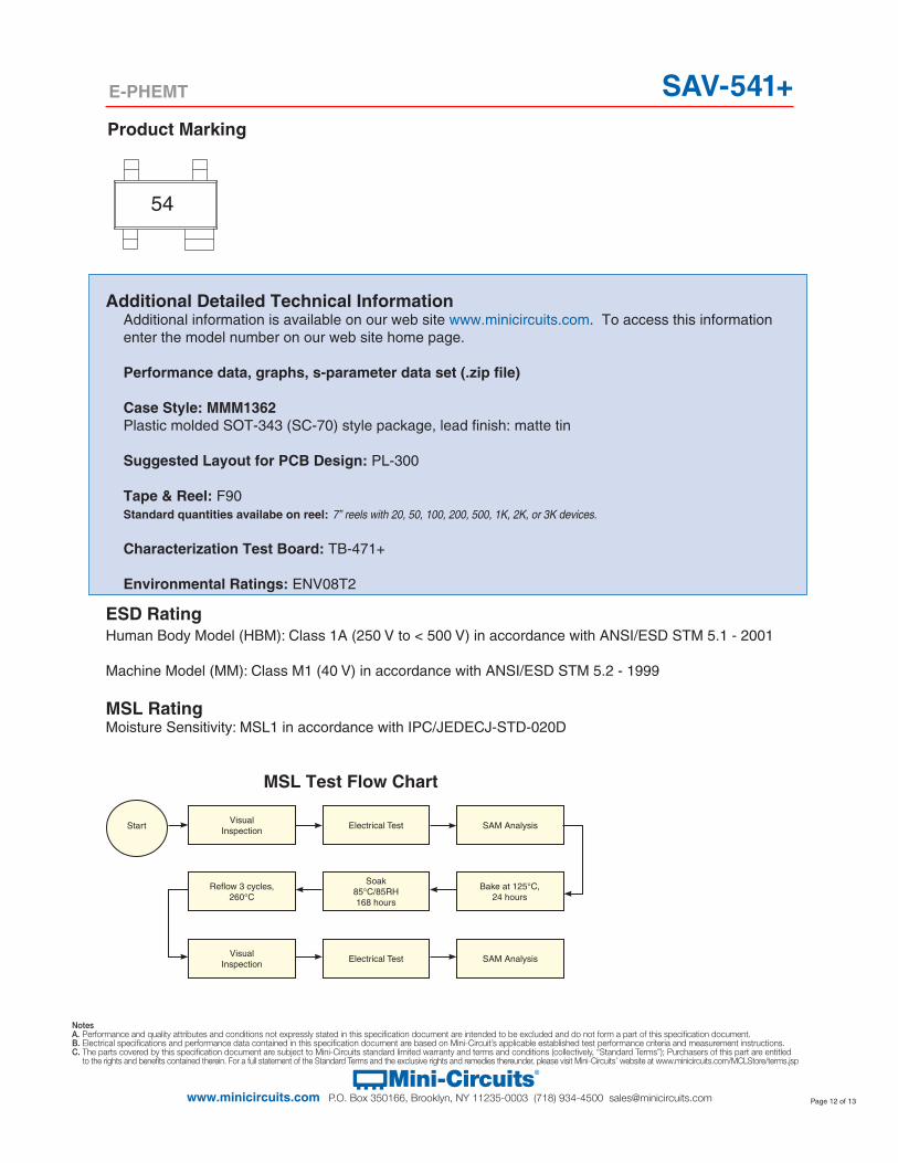
Additional Detailed Technical InformationAdditional information is available on our web site www.minicircuits.com. To access this information enter the model number on our web site home page.
Performance data, graphs, s-parameter data set (.zip file)
Case Style: MMM1362Plastic molded SOT-343 (SC-70) style package, lead finish: matte tin
Suggested Layout for PCB Design: PL-300
Tape & Reel: F90Standard quantities availabe on reel: 7” reels with 20, 50, 100, 200, 500, 1K, 2K, or 3K devices.
Characterization Test Board: TB-471+
Environmental Ratings: ENV08T2
Product Marking
54
ESD RatingHuman Body Model (HBM): Class 1A (250 V to < 500 V) in accordance with ANSI/ESD STM 5.1 - 2001
Machine Model (MM): Class M1 (40 V) in accordance with ANSI/ESD STM 5.2 - 1999
MSL RatingMoisture Sensitivity: MSL1 in accordance with IPC/JEDECJ-STD-020D
VisualInspection
Electrical Test SAM Analysis
Reflow 3 cycles,260°C
Soak85°C/85RH168 hours
Bake at 125°C,24 hours
VisualInspection
Electrical Test SAM Analysis
Start
MSL Test Flow Chart
E-PHEMT SAV-541+
NotesA. Performance and quality attributes and conditions not expressly stated in this specification document are intended to be excluded and do not form a part of this specification document. B. Electrical specifications and performance data contained in this specification document are based on Mini-Circuit’s applicable established test performance criteria and measurement instructions. C. The parts covered by this specification document are subject to Mini-Circuits standard limited warranty and terms and conditions (collectively, “Standard Terms”); Purchasers of this part are entitled to the rights and benefits contained therein. For a full statement of the Standard Terms and the exclusive rights and remedies thereunder, please visit Mini-Circuits’ website at www.minicircuits.com/MCLStore/terms.jsp
Mini-Circuits®
www.minicircuits.com P.O. Box 350166, Brooklyn, NY 11235-0003 (718) 934-4500 [email protected] Page 13 of 13
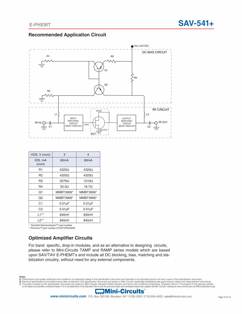
Recommended Application Circuit
VDS, V (nom) 3 4
IDS, mA (nom)
60mA 60mA
R1 4320Ω 4320Ω
R2 4320Ω 4320Ω
R3 3570Ω 1210Ω
R4 33.2Ω 16.7Ω
Q1 MMBT3906* MMBT3906*
Q2 MMBT3906* MMBT3906*
C1 0.01µF 0.01µF
C2 0.01µF 0.01µF
L1** 840nH 840nH
L2** 840nH 840nH
R1
Q1
Q2
R4
R2
GATE
DRAIN
C1 C2
INPUT MATCHING
CIRCUIT(MUST PASS DC)
OUTPUT MATCHING
CIRCUIT(MUST PASS DC)
R3
Vcc (+5V DC)
RF-IN RF-OUT
DC BIAS CIRCUIT
DUT
L1 L2
SOURCE
RF CIRCUIT
* Fairchild Semiconductor™ part number** Piconics™ part number CC45T47K240G5
Optimized Amplifier CircuitsFor band specific, drop-in modules, and as an alternative to designing circuits,please refer to Mini-Circuits TAMP and RAMP series models which are based upon SAV/TAV E-PHEMT’s and include all DC blocking, bias, matching and sta-bilization circuitry, without need for any external components.


![NATURAL SCIENCES D568/12 ADMISSIONS ASSESSMENT 40 … · Ω, 2 Ω, 4 Ω, 8 Ω, 16 Ω, 32 Ω, 64 Ω, … connected in parallel with the cell. ... [2 marks] Answer: ... is used as the](https://img.dokumen.tips/doc/110x75/5f2363f7b03d7e4ce06bc15b/natural-sciences-d56812-admissions-assessment-40-2-4-8-16-32.jpg)