Embed Size (px)
Citation preview

UCRL-16231
UNIVERSITY OF CALIFORNIA
Lawrence Radiation LaboratoryBerkeley, California
AEC Contract No. W-7405-eng-48
SEMICONDUCTOR DETECTORS
forNUCLEAR SPECTROMETRY*
Fred S. Goulding
July 30, 1965
*Lectures to be given at Herceg-Novi, Yugoslavia, August, 1965.

TO:
FROM:
Subject:
UNIVERSITY OF CALIFORNIALawrence Radiation Laboratory
Berkeley, California
AEC Contract No. W-7405-eng-48
September 24, 1965
ERRATA
All recipients of UCRL-16231
Technical Information Division
UCRL-16231, "Semiconductor Detectors for NuclearSpectrometry," by Fred S. Goulding, dated July 30, 1965.
Please make the following corrections on subject report.
Figures 3-2 and 3-3 should be replaced by the attached figures.
Page 91, line 12 should be changed to read"The Fano factor established by these measurements is.30 ± 0.03 which is entirely consistent with the approximatevalue of 0.32 derived from Van Roosbroeck’s curves."
UNIVERSITY OF CALIFORNIADepartment of PhysicsBERKELEY 4, CALIFORNIA
RETURN POSTAGE GUARANTEED

-ii- UCRL-16231
SEMICONDUCTOR DETECTORS FOR NUCLEAR SPECTROMETRY
Table of Contents
List of Figures . . . . . . . . . . . . . . . . . . . . . . . . . . . . v
Foreword . . . . . . . . . . . . . . . . . . . . . . . . . . . . . . . vii
1.1 Introduction . . . . . . . . . . . . . . . . . . . . . . . . . . . 1
1.2 Properties of Solid-State Detector Materials . . . . . . . . . . . 4
1.3 Semiconductor Properties of Silicon and Germanium . . . . . . . . . 7
1.3.1 Intrinsic Material Properties . . . . . . . . . . . . . . . 7
1.3.2 Extrinsic Material General Properties . . . . . . . . . . . 10
1.3.3 More Detailed Behavior of Carriers in Extrinsic Material . . 13
1.4 Junctions in Semiconductors . . . . . . . . . . . . . . . . . . . . 17
1.4.1 Descriptive Junction Theory . . . . . . . . . . . . . . . . 17
1.4.2 Reverse Biased Junction . . . . . . . . . . . . . . . . . . 19
1.4.3 Junction Capacitance . . . . . . . . . . . . . . . .. . . . 20
1.4.4 Junction Leakage Currents . . . . . . . . . . . . . . . . . 21
1.4.5 P-I-N Junctions . . . . . . . . . . . . . . . . . . . . . . 24
1.4.6 Metal to Semiconductor Surface Barrier Junctions . . . . . . 25
Lecture 1. Figure Captions . . . . . . . . . . . . . . . . . . . . . . 29
2.1 Introduction . . . . . . . . . . . . . . . . . . . . . . . . . . . 39
.
.
2.2 Discussion of Purity of Semiconductor Materials . . . . . . . . . . 40
2.3 Diffused Silicon Detectors . . . . . . . . . . . . . . . . . . . 41
2.3.1 Elementary Considerations . . . . . . . . . . . . . . . . . 41
2.3.2 Surface Properties . . . . . . . . . . . . . . . . . . . . . 45
2.3.3 Preparation of Diffused Detectors . . . . . . . . . . . . . 49

-iii- UCRL-16231
2.4 Compensation by Lithium Drifting . . . . . . . . . . . . . . . . . 53
2.4.1 General Principles . . . . . . . . . . . . . . . . . . . . 53
2.4.2 Secondary Effects in Lithium Drifting . . . . . . . . . . . 57
2.4.3 Surface Effects in Lithium-Drifted Devices . . . . . . . . 60
2.4.4 Preparation of Lithium-Drifted Silicon Detectors . . . . . 60
2.4.5 Preparation of Lithium-Drifted Germanium Detectors . . . . 64
2.5 Detectors Not Employing Junctions . . . . . . . . . . . . . . . . 67
2.6 Making The Choice Between Detector Types . . . . . . . . . . . . . 69
Lecture 2. Figure Captions . . . . . . . . . . . . . . . . . . . . . 72
3.1 Introduction . . . . . . . . . . . . . . . . . . . . . . . . . . . 87
3.2 Statistical Spread in the Detector Signal . . . . . . . . . . . . 88
3.3 Electrical Noise Sources . . . . . . . . . . . . . . . . . . . . . 91
3.4 Effect of Amplifier Shaping Networks . . . . . . . . . . . . . . . 95
3.5 Vacuum Tubes as the Input Amplifying Device . . . . . . . . . . . 103
3.6 Alternative Lou Noise Amplifying Elements . . . . . . . . . . . . 107
3.7 Additional Sources of Signal Amplitude Spread . . . . . . . . . . 113
3.7.1 Noise Contribution of Main Amplifier . . . . . . . . . . . 113
3.7.2 Gain Drifts . . . . . . . . . . . . . . . . . . . . . . . . 114
3.7.3 High Counting Rates . . . . . . . . . . . . . . . . . . . . 114
3.7.4 Finite Detector Pulse Rise Time . . . . . . . . . . . . . . 115
Lecture 3. Figure Captions . . . . . . . . . . . . . . . . . . . . . 118
4.1 Detector Pulse Shape . . . . . . . . . . . . . . . . . . . . . . . 138
4.1.1 Pulse Shape Due to a Single Hole-Electron Pair in P-I-N Detector . . . . . . . . . . . . . . . . . . . . . . 139
4.1.2 Pulse Shape Due to a Single Hole-Electron Pair in ap-n Junction Detector . . . . . . . . . . . . . . . . . . . 141
4.1.3 Pulse Shape Distribution for Gamma-rays in GermaniumP-I-N Detectors at 77°K . . . . . . . . . . . . . . . . . . 146
4.1.4 Pulse Shape Distribution for Protons and Alpha-ParticlesStopping in a Lithium-Drifted Silicon Detector . . . . . . 149

-iv- UCRL-16231
4.2 Radiation Damage in Detectors . . . . . . . . . . . . . . . . . . . 150
4.2.1 Damage Mechanism . . . . . . . . . . . . . . . . . . . . . . 150
4.2.2 Consequences of Damage in p-n Junction Detectors . . . . . . 153
4.2.3 Consequences of Damage in Lithium-Drifted Silicon Detectors 156
Acknowledgements . . . . . . . . . . . . . . . . . . . . . . . . . . . 159
Lecture 4. Figure Captions . . . . . . . . . . . . . . . . . . . . . . 160
References . . . . . . . . . . . . . . , . . . . . . . . . . . . . . . 169
Table 1.1 Some Properties of Silicon and Germanium . . . . . . . . 27
Table 1.2 Impurities in Ge & Si . . . . . . . . . . . . . . . . . 28
Table 3.1 Noise Integral and Peak Response of Several Networks . . 116
Table 3.2 Input Pulse Shape Dependancc of Several Shaping Networks 117

Fig. 1.1 Unit Cell of Single Crystal Si and Ge . . . . . . . . . . . 30
Fig. 1.2 Variation of Mobility with Temperature in Pure Samples . . . 31
Fig. 1.3 Resistivity - Impurity Concentration for Si . . . . . . . . 32
Fig. 1.4 Resistivity - Impurity Concentration for Ge . . . . . . . . 33
Fig. 1.5 Effect of Impurities on Mobility . . . . . . . . . . . . . . 34
Fig. 1.6 Resistivity Temperature Relation for an Extrinsic Silicon
Fig. 1.7 Diagram of a P-N Junction in Equilibrium . . . . . . . . . . 36
Fig. 1.8 A Reverse Biased P-N Junction . . . . . . . . . . . . . . . 37
Fig. 1.9 An N+ PP+ Punch-Through Diode . . . . . . . . . . . . . . . 38
Fig. 2.1 Depletion Layer Thickness Curves for N and P-Type Silicon . 73
Fig. 2.2 Illustration of Charge Injection at Rear Contact . . . . . . 74
Fig. 2.3 Models of Surface Layers at Junction Edge . . . . . . . . . 75
Fig. 2.4 Effect of Ambients on Leakage Current of a Junction . . . . 76
Fig. 2.5 Guard-Ring Structure . . . . . . . . . . . . . . . . . . . . 77
Fig. 2.6 Typical Leakage Curve for Guard-Ring Detector . . . . . . . 78
Fig. 2.7 Steps in Preparing a Planar Junction Device . . . . . . . . 79
Fig. 2.8 Distribution of Lithium at States of Lithium Drift . . . . . 80
Fig. 2.9 Drifted Region Thickness - Time Relationship for Silicon . . 81
Fig. 2.10 Drifted Region Thickness - Time Relationship for Germanium . 82
Fig. 2.11 Illustration of Silicon Wafer Prior to Drifting . . . . . . 83
Fig. 2.12 Cutaway View of Lithium-Drifted Silicon Detector . . . . . . 84
Fig. 2.13 Germanium-Lithium-Drift Unit . . . . . . . . . . . . . . . . 85
Fig. 2.14 Diagram of Germanium Detector Holder and Cryostat . . . . . 86
-v- UCRL-16231
LIST OF FIGURES
Sample . . . . . . . . . . . . . . . . . . . . . . . . . . 35

Fig. 3.1 Diagrammatic Representation of Energy Loss Process . . . . 119
Fig. 3.2 Calculated Yield and Fano Factor . . . . . . . . . . . . . 120
Fig. 3.3 Resolution-Energy Relationship Data for Germanium . . . . . 121
Fig. 3.4 Typical Electronics for Spectroscopy . . . . . . . . . . . 122
Fig. 3.5 Simplified Input Equivalent Circuits . . . . . . . . . . . 123
Fig. 3.6 Typical Shaping Networks and Their Frequency Response . . . 124
Fig. 3.7 Pulse Response of Several Networks (Unit Function Input) . 125
Fig. 3.8 EC-1000 Preamplifer . . . . . . . . . . . . . . . . . . . . 126
Fig. 3.9 Noise Performance Curves for EC-1000 Preamplifer . . . . . 127
Fig. 3.10 EC-1000 Preamplifer: Effect of Double Integrator . . . . . 128
Fig. 3.11 EC-1000 Preamplifer . . . . . . . . . . . . . . . . . . . . 129
Fig. 3.12 EC-1000 Preamplifer Rise Time Curves . . . . . . . . . . . 130
Fig. 3.13 Bulk Field-Effect Transistor (N-Channel Type Illustrated) . 131
Fig. 3.14 General Purpose Field Effect Transistor Preamplifer . . . . 132
Fig. 3.15 Predicted Noise Behavior of Field-Effect Transistor at 300°K 133
Fig. 3.16 Predicted Noise Behavior of Field Effect Transistor at 77°K 134
Fig. 3.17 Circuit for Low Temperature Tests on Field-Effect Transistors 135
Fig. 3.18 Noise Performance of TIS-05 Field Effect Transistor . . . . 136
Fig. 3.19 Noise Performance of Amelco 2N3458 Field-Effect Transistor. 137
Fig. 4.1 Collection of Hole-Electron Pair in a p-i-n Detecotr . . . 161
Fig. 4.2 Signal Output Due to a Single Electron Hole Pair in a
Fig. 4.3 Collection of Hole-Electron Pair in a P-N Junction . . . . 163
Fig. 4.4 Signal Output due to a Single Electron-Hole Pair in a
Fig. 4.5 Expected Range of Pulse Shapes from p-i-n Germanium
Fig. 4.6 Distribution in Triggering Delays of a Discriminator set to
Fig. 4.7 Detector Pulse Shape for Alphas . . . . . . . . . . . . . . 167
Fig. 4.8 Frenkel Defect Production by Alphas and Protons (Silicon) . 168
-vi- UCRL-16231
p-i-n Detector . . . . . . . . . . . . . . . . . . . . . . 162
P-N Junction Detector . . . . . . . . . . . . . . . . . . . 164
Detector at 77°K . . . . . . . . . . .. . . . . . . . . . . 165
β-Peak Pulse Amplitude from a Germanium Detector . . . . . 166

-vii- UCRL-16231
SEMICONDUCTOR DETECTORS FOR NUCLEAR SPECTROMETRY
Fred S. Goulding
University of CaliforniaLawrence Radiation Laboratory
Berkeley, California
July 30, 1965
FOREWORD
These lectures were prepared for presentation at the Summer School
for Physicists to be held in Herceg-Novi, Yugoslavia, August, 1965. For
the most part they constitute a collection of essential information on
the detectors and associated systems. Although some important contri-
butions by other groups to the topic are discussed, no effort has been
made to present a detailed review of the voluminous literature on the
subject. Therefore, the notes given here must be regarded largely as
an account of the work of one group in this field. Very few experimental
results obtained with semiconductor detector spectrometers are included
as this material should be covered by other speakers at the meeting.

-1- UCRL-16231
DESCRIPTIVE THEORY OF SEMICONDUCTORSLECTURE 1.
Fred S. Goulding
Lawrence Radiation LaboratoryUniversity of CaliforniaBerkeley, California
July 30, 1965
1.1 INTRODUCTION
Much of nuclear physics research is concerned with the measurement of
the energy of radiation emitted by nuclei undergoing energy transitions.
Consequently, the development of nuclear structure studies has depended
largely upon techniques of accurate energy measurement. The most precise
energy measurements are based on the effect of magnetic fields in bending
the path of electrically charged particles. However, the poor geometrical
efficiency and the inability of such devices to allow simultaneous measure-
nents over a wide range of energies restrict the usefulness of these tech-
niques except for primary standard energy measurements. The high data
accumulation rate of a pulse amplitude analyzer fed by a detector which
totally absorbs photons or particles to produce a signal linearly propor-
tional to the energy absorbed has made these techniques very useful for
general nuclear energy measurements. Gridded ionization chambers and
scintillation detectors have been used in such systems and, in recent years,
semiconductor detectors have assumed increasing importance.
In our laboratory, semiconductor detectors have almost completely
replaced scintillation and gaseous detectors in all nuclear structure work
ranging from work with natural alpha, beta and gamma radiations to nuclear
reaction studies in the 10 to 100 MeV range. The reason for this sudden
change lies primarily in the improvement in energy resolution obtained by

Lecture 1. -2- UCRL-16231
use of these detectors, an improvement which ranges from about 2:1 for low-
energy alpha particles to 10:1 for high-energy (~100 MeV) alpha particlesIand 20:1 for gamma-rays of medium energy (~600 keV). As compared with
gaseous detectors the small size of semiconductor detectors and theirIability to totally absorb the energy of fast electrons and other particles
are additional factors in favour of semiconductor detectors. When compared
with NaI (T1) and other scintillator crystals, the gamma-ray efficiency of
presently available semiconductors is poor, in general, but our experience
is that good energy resolution is more important than very high efficiency
which can usually be compensated for by using more active sources.
While a detailed examination of the problems of energy spread in detector
systems will be made in Lecture #3 it is desirable that we briefly review
here the basic reasons for the improved energy resolution in semiconductor
detectors. In gaseous detector systems electrical noise in the pulse
amplifier and statistical fluctuations of ion-pair production in the detector
both limit the accuracy of energy measurements. For a 5 MeV alpha-particle
(a typical particle in ion chamber applications) about 2 x 10⁵ ion pairs will
be produced assuming that 25 eV are required on the average to produce an ion
pair. If normal statistical variations existed in this number, an RMS fluctu-
ation of about 500 ion pairs might be expected. As pointed out by Fano1,2 RMS
fluctuations will be less than this by a factor of about 0.6.* Therefore, RMS
fluctuation will be about 300 ion pairs. The electrical noise in existing . .high quality amplifiers contributes an effective RMS input signal fluctuation
of about 300 ion pairs also and by adding these two sources of spread in quad-
rature we find that the total effective fluctuation should be about 420 ion
pairs RMS or 1000 ion pairs** full width at half maximum (FWHM is used in the
*The Fano factor (= Mean Square Fluctuation
Av. No. of Ion Pairs
) is assumed here to be 0.4.
**For Gaussian noise the ratio of FWHM/RMS is about 2.3.

Lecture 1. -3- UCRL-16231
remainder of this text). The theoretical FWHM energy resolution for gaseous
ion chambers is therefore about 20 keV. In most practical situations this
result is not realized and 30-40 keV is more common.
Scintillation detectors suffer from quite different sources of signal
spread. The inefficiency involved in the scintillation mechanism, light
collection and photo-emission from the cathode of the photomultiplier, results
in large statistical fluctuations in the number of photo-electrons emitted by
the photo-cathode for a given amount of energy absorbed in the scintillating
crystal.* In the case of a NaI (T1) scintillator-photomultiplier system, at
least 300 eV of energy is absorbed in the crystal for every photo-electron
released. For a 300 keV gamma-ray this results in a FWHM spread of about
25 keV or almost 10%. The energy distribution of electrons produced in the
scintillatar by one gamma-ray may differ considerably from that produced by
another and since the scintillator light output is not a linear function of
electron energy a further spread in light output for gamma-ray interactions
is introduced.4,5 This effect becomes important for high gamma-ray energies,
Fortunately the phototube is a noiseless amplifying device and, apart from
minor contributions due to statistical variations in the numbers of electrons
released by the secondary emission surfaces, it does not further degrade the
output signal.
Detectors employing direct collection of ionization in certain solids
possess one striking fundamental advantage over scintillation and gaseous
detectors. In single crystal semiconductors of the types considered here, a
hole-electron pair is produced for about every 3 electron volts (on the average)
absorbed from the radiation. This figure is almost a factor of 10 smaller than
the equivalent quantity for gaseous detectors and a factor of 100 smaller than
*We will not deal here with the details of the scintillation mechanism.Refer to Ref. 3 for details.

Lecture 1 -4- UCRL-16231
that for scintillation detectors. For this reason, statistical fluctu-
ations in the charge prdouction process in the detector are small. Moreover,
since the charge flow in the detector is almost 10 times larger than in the
gaseous detector, the effect of pulse amplifier noise is reduced by a similar
factor. Unfortunately collection of ionization in solids is, in general, a
difficult process and some rather rigid requirements must be placed upon the
character of the solid. Our next section will discuss these requirements
and the characteristics of suitable material.
1.2 PROPERTIES OF SOLID-STATE DETECTOR MATERIALS
IWe will assume initially that the detector consists of a rectangular
block of material with electrodes in good electrical contact with two opposite
faces of the block. A potential is applied to the electrodes to produce an
electric field in the solid which will (hopefully) sweep out any electrical
carriers produced by an ionizing event. Carriers of both polarities (negative
electrons and positive holes) will be produced in equal numbers by the ionizing
event. As we wish to measure the quantity of ioniaation produced (which is
proportional to the energy absorbed from the radiation) it is important that
the charge flow in the external circuit of the detector be equal to the total
ionization or to some definite fraction of it. In practice the latter possi-
bility is impossible and we are forced to meet the first condition.
The material properties of importance are as follows:
(a) The average energy ε required to produce a hole-electron pair should
be as small as possible. The reasons for this requirement are
apparent from the previous discussion. A portion of ε is used to
lift electrons through the band gap from the conduction to valency

Lecture 1 -5- UCRL-16231
(b)
(c)
band and the remainder is wasted in thermal losses (principally
to optical modes of vibration) in the solid. As a general rule
this factor favors materials with small band-gaps but the situation
is complicated by other factors.
The material should contain few free carriers at the operating
temperature as such carriers will be swept to the electrodes in
the same way as those produced by the ionizing events and will tend
to spread and conceal the wanted signals. This requirement immedi-
ately eliminates conductors from consideration and since, in semi-
conductors and insulators, the thermal activation of electrons
across the band-gap is a mechanism for production of free carriers,
it, favors wide band-gap materials. Since this conflicts with
property (a) a compromise is necessary and the ideal compromise will
depend upon the operating temperature. To be of interest materials
must produce thermal generation currents in the volume of the
detector smaller than 10-7 amperes. For some applications even
smaller currents than this are required.
The previous requirement suggests that an insulator might be ideal
if a rather high value of ε is tolerable. However, it is very
important that the material used should not contain significant
numbers of trapping centers capable of holding electrons or holes
produced by the ionizing events. If this were to happen we would
lose part of our signal with disastrous consequences. This require-
ment immediately narrows down the choice of materials to those
available as almost perfect single crystals (free of impurities to
levels of about 1 part in 109 or better and free of crystal imperfec-
tions). Moreover materials having wide band-gaps tend to contain

Lecture 1 -6- UCRL-16231
many deep trapping centers and are therefore eliminated on this
count. We will characterize the trapping process by the trapping
lifetime of a carrier τT which is the average time a carrier
exists in a free state before being trapped
(d) Recombination of holes and electrons during the charge collection
process must be very small. In practice, recombination occurs
primarily through the intermediary of trapping at energy levels
near the middle of the band-gap. It is of interest to note that
this is related to the property (b) as the primary source of
thermally generated conduction electrons in semiconductors is a
double-jump process whereby an electron in the valency band is
excited info a trapping level near the middle of the band gap and
then re-excited into the conduction band. Recombination in a semi-
conductor is characterized by the carrier lifetime τR and we desire
this to be large compared with the charge collection time.
(e) The effect of both trapping and recombination must be related to
the carrier collection time τC if the magnitude of the carrier loss
is to be evaluated. Ideally the collection time τC should be very
short which demands that both holes and electrons should be highly
mobile in the lattice. Also the material should be able to support
high electric fields without secondary ionization resulting. In
most cases, surface effects limit the applied voltage more than
bulk effects.
(f) The nuclear properties of a material are also important in its
application for detectors. Other things being equal one would
like to use materials containing elements of high atomic number to

Lecture 1 -7- UCRL-16231
improve the absorbtion properties of the detector. These require-
ments are secondary to the electrical requirements discussed in
the previous paragraphs which must be met if satisfactory detection
is to be achieved. However, the nuclear requirements will certainly
influence future work on materials and have already resulted in the
use of germanium for gamma-ray detectors in preference to silicon
which, in most other respects, is a preferable material.
1.3 SEMICONDUCTOR PROPERTIES OF SILICON AND GERMANIUM
Only two materials are known to approach the requirements of the previous
section. Early work in the semiconductor device area (e.g., transistors) was
based largely on using germanium and the extensive program of research and
development on this material resulted in it becoming available in the form
of highly pure single crystals. Later, emphasis on higher temperatures of
operation for semiconductor devices resulted in silicon becoming available
with quality equal or even superior to germanium. These two materials are
now the only ones we are able to use for accurate nuclear spectrometry. We
will now digress from our main topic to consider the properties of silicon
and germanium as examples of a general class of semiconductors.
1.3.1 Intrinsic Material Properties
Both silicon and germanium crystals are particularly simple in their
structure. Fig. 1.1 shows the arrangement of the atoms in a simple valency
bond model of a pure crystal of silicon or germanium. Each atom (valency 4)
is seen to have its valency bonds oriented equally in space and to donate
a single electron to each bond with its four neighbors. Each bond therefore
contains a pair of electrons giving a particularly stable structure.

Lecture 1 -8- UCRL-16231
At very low temperatures all valency electrons are bound into the
structure and no electrons are available to take part in electrical
conduction. Therefore these materials are insulators at these temperatures.
At higher temperatures a small number of the covalent bonds are broken by
thermal excitation so that electron-hole pairs are produced in the material.
In the energy band model, electrons are said to be thermally excited from
the valency to conduction band. The quantities of such electron-hole
pairs clearly depend upon the temperature and the band-gap (binding energy
in the valency bond model). Under normal conditions the number ni of con-
duction electrons in the material (called intrinsic since no impurities
are present) is given by:
where A is a constant for a given material,
T is the absolute temperature (°K),
Eg is the band gap,
k is Boltzman's constant.
At normal temperatures the exponential term dominates the temperature
dependence.
Once an electron is in the conduction band it is influenced by any
electric field applied to the crystal. In normal electric fields this
influence is small compared with effects due to the fields produced by
atoms in the lattice itself but the applied electric field causes a slow
drift of the electrons whereas the effects of the crystal atoms are random
Lecture 1 -9- UCRL-16231
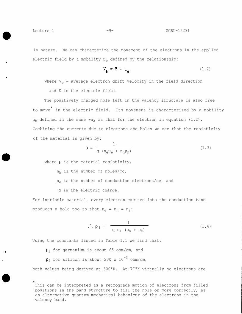
in nature. We can characterize the movement of the electrons in the applied
electric field by a mobility µe defined by the relationship:
(1.2)
where Ve = average electron drift velocity in the field direction
and E is the electric field.
The positively charged hole left in the valency structure is also free
to move* in the electric field. Its movement is characterized by a mobility
µh defined in the same way as that for the electron in equation (1.2).
Combining the currents due to electrons and holes we see that the resistivity
of the material is given by:
ρ =1
q (neµe + nhµh) (1.3)
where ρ is the material resistivity,
nh is the number of holes/cc,
ne is the number of conduction electrons/cc, and
q is the electric charge.
For intrinsic material, every electron excited into the conduction band
produces a hole too so that ne = nh = ni:
... ρ i =
1
q ni (µh + µe) (1.4)
Using the constants listed in Table 1.1 we find that:
ρi for germanium is about 65 ohm/cm, and
ρi for silicon is about 230 x 10-3 ohm/cm,
both values being derived at 300°K. At 77°K virtually no electrons are
*This can be interpreted as a retrograde motion of electrons from filledpositions in the band structure to fill the hole or more correctly, asan alternative quantum mechanical behavicur of the electrons in thevalency band.

Lecture 1 -10- UCRL-16231
excited into the conduction band and intrinsic silicon and germanium are
excellent insulators at that temperature.
The carrier mobility µ, as well as ni, is temperature dependent. The
dependance of µ on temperature in very pure crystals of good quality is
dominated by lattice scattering (i.e., interactions of thermal lattice
vibrations with the electron wave travelling in the structure). As the
temperature is reduced, the mobility increases. For example, µh for
silicon changes from 480 cm2/V. sec at 300°K to about 2 x 104 cm2/V. sec
at 77°K. The temperature dependance of µe, µh and ni is indicated in
Table 1. Fig. 1.2 shows the bahaviour of µe and µh in silicon and
germanium over a wide temperature range.
1.3.2 Extrinsic Material General Properties
In practice, semiconducting materials of sufficient purity to be
regarded as intrinsic, particularly at low temperatures, are not available
to us. Generally speaking, the term intrinsic is used rather loosely to
imply that electrical conduction is dominated by thermally excited electron-
hole pairs rather than by electrons or holes produced by impurities. Thus,
at high enough temperatures we can refer to any semiconductor as being
intrinsic. In the case of germanium it is possible to purify the material
to the degree where the material is intrinsic at room temperature. To
accomplish this, impurities* must be reduced below about 1013 atoms/cc
(i.e., 1 part in 5 x 10⁸) which is just possible. For conduction in silicon
to be considered intrinsic at room temperature, the impurity concentration*
would have to be reduced to about 1010 atoms/cc (i.e., 1 part in 5 x 10¹¹)
which is not practicable. Therefore, for most practical purposes, we have
*We refer here only to electrically active impurities.

Lecture 1 -11- UCRL-16231
to deal with materials in which conduction is dominated by electrical
carriers introduced by impurities in the silicon or germanium. This is
known as extrinsic material and the conduction is termed extrinsic too.
The electrically active impurities most commonly deliberately intro-
duced into semiconductors are elements of valency 3 or 5 which can sub-
stitute for silicon atoms at lattice sites. Thinking in terms of the
valency bond model we can regard a valency 5 atom (e.g., phosphorous,
arsenic, antimony) which replaces a silicon atom in the lattice as
supplying the electrons to complete the co-valent bond structure while
the fifth electron associated with the impurity atom is only very loosely
bound to its parent atom by Coulomb attraction. This attraction is very
small partly due to the fact that the atom is embedded in a medium of high
dielectric constant (12 for silicon, 16 for germanium). At normal tempera-
tures the spare electron is thermally excited into the conduction band so
that we now have a free electron and a fixed localized positive charge
embedded in the lattice in the vicinity of the impurity atom. Such impur-
ities are called donors and, since the electrical conduction in such
materials is dominated by negative charge carriers, the material is said
to be n-type. Conversely, replacement of silicon atoms by valency 3 atoms
(e. g., boron, aluminum, gallium, and indium) produces holes and fixed
negative charge centers; the material is p-type and the impurity is called
an acceptor. In an energy band model the effect of donors is to introduce
permitted discrete levels (localized in the vicinity of the impurity atoms)
in the forbidden gap close to the conduction band. Conversely the effect
of acceptors is to introduce levels close to the valency band. Donors and
acceptors such as these are easily ionized. Table 1.2 lists the ionization
energy for some of these cases.

Lecture 1 -12- UCRL-16231
In detector technology we are particularly concerned with a number of
other types of center in the lattice. For the present we will note that
an interstitial atom can act as a donor or acceptor giving free holes
and/or electrons. A good example of this is lithium which acts as a shallow*
interstitial donor in silicon and germanium. Certain other impurities
acting in a substitutional or interstitial role like gold in silicon or
copper and nickel in germanium introduce acceptor and/or donor levels near
the middle of the forbidden gap. Note that certain impurities can introduce
both donor and acceptor levels. We can picture this as depending upon the
position occupied by the impurity atom in the lattice. For example, gold
introduces both an acceptor and donor level near the middle of the energy
gap. As one might expect, a valency 2 substitutional impurity tends to
produce a double acceptor while a valency 6 substitutional impurity tends
to produce a double donor.
Another matter of concern to us is the number of traps in the material.
These traps may arise due to impurity centers or crystal imperfections
(vacancies, dislocations, etc.) and may exhibit preferential trapping pro-
perties for either holes or electrons. The traps are of interest in that
they provide intermediate levels in the forbidden gap through which recom-
bination and generation processes can take place. Moreover, if the traps
are selective for holes (or electrons) and the trapped carriers are not
easily re-excited, localized storage of electrical charge may occur and
this may inhibit collection of carriers in the device. This is particularly
important in low temperature operation of devices and is the cause of the
phenomena generally referred to as polarization in detectors.
*The term shallow implies that the level introduced by the impurity isclose to the conduction band (donor) or valency band (acceptor).

Lecture 1 -13- UCRL-16231
1.3.3 More Detailed Behaviour of Carriers in Extrinsic Material.
Considering, for the moment, intrinsic material in equilibrium, an
average number ni electrons occupy the conduction band and a similar
number of holes exist in the valency band. We have to remember that this
equilibrium results from the balance between excitation of electrons into
the conduction band (called generation) and by electrons falling back into
holes in the valency band (recombination). The rates of generation and
recombination can be increased by introducing traps into the forbidden
gap as these traps provide the potential for a double step process which
can clearly proceed at a faster rate than if electrons have to jump across
the whole energy gap in one step. Traps at the center of the energy gap
are most effective in increasing the generation and recombination rate as
the two steps are then equal. Despite the increased rate of recombination
and generation the equilibrium density of electrons and holes is the same
in material containing large or small numbers of such traps. In a non-
equilibrium condition, however, in which an applied electric field sweeps
out carriers immediately they are produced, the high generation rate induced
by traps considerably increases the leakage current and, from this point of
view, traps (particularly in mid-band) are undesirable. We will pursue
this point later.
Now let us examine the introduction of a small amount of a donor impurity
into the semiconductor. This increases the number of electrons from ni to n.
Let the consequent alteration in the hole population be from ni to p. The
recombination rate between hole and electrons must be proportional to the
product (n · p) of the numbers of such carriers present in the material. We
can assume that the generation rate is only dependent upon valency bonds

which are far more numerous than the impurity atoms. Since the thermal
generation rate (at impurity levels commonly encountered) is therefore the
same as for intrinsic material and the recombination rate in such material
is proportional to ni2 we can write:
2n · p = ni (1.5)
Thus we see that the effect of increasing the electron population by
adding donors is to suppress the hole population to satisfy equation (7.5).
Similarly, if we introduce acceptors, the electron population is reduced.
These remarks apply at a fixed temperature; if the temperature is changed,
ni must be chosen for the new temperature.
To appreciate the effect of this minority carrier suppression by
introducing majority carriers we may examine the case of silicon at room
temperature 300°K). In this case, ni = 1.5 x 10¹⁰/cc. Let us now
introduce 1.5 x 10¹¹ donors/cc (i.e., about one atom in 4 x 10¹⁰). The
hole population will now only be 1.5 x 10⁹ - a factor of 100 smaller than
the electron population. Conduction in such a sample is now dominated
by electrons and the resistivity is given by:
ρ = 1 (1.6)
neµe q
In our example, ρ would be 35000 ohm/cm. In practice removal of impurities
to this extent is impractical. However, the float-zone process in silicon
can produce material in the 10000 ohm/cm (p-type) region. Figs. 1.3 and
1.4 show the resistivity as a function of donor and acceptor concentra-
tion for silicon and germanium.
We must now examine the behaviour of these extrinsic semiconductors
as the temperature is changed. At high temperatures (~150°C for very pure
silicon and ~60°C for very pure germanium) the value of ni increases so

Lecture 1 -15-
that, in the doping range of interest to us (~ 1012 to 1016 impurity
atoms/cc) electrical conduction hecomes dominated by thermally excited
carriers and the material is called intrinsic. As the temperature is
lowered, conduction is dominated by the majority carriers and the quantity
of these remains essentially the same down to temperatures at which the
donor or acceptor centers become unionized (i.e., ~ 10 to 50°K). In
lightly doped material the mobility is determined by lattice scattering
and the mobility-temperature relationships shown in Table 1.1 apply.
However, as the lattice scattering becomes smaller the effect of the
Coulomb attraction of impurity atoms becomes more important and mobility
becomes determined by impurity scattering. Even at moderate doping
levels this effect causes the mobility to level off or decrease below
about 200°K. Fig. 1.5 shows the mobility temperature relationship for
some samples. In closing these remarks on mobility we must point out
that, since the number of carriers remains essentially constant in extrinsic
semiconductors over a wide range of temperatures while the mobility increases
as the temperature decreases in the range where lattice scattering is
dominant, the result is that the material exhibits a high positive
temperature coefficient of resistance as seen in Fig. 1.6 over part of
the temperature range. This is a surprising result on the basis of
traditional views of semiconductors.
In the preceeding discussion we assumed that the extrinsic semiconductor
was produced by adding either an acceptor or donor to intrinsic material.
Usually, however, we are dealing with materials containing both donor and
acceptor atoms. Since we have seeen that the addition of donors to a
material produces the hole population so that equation (1.5) is satisfied,
it is obvious that addition of donors compensates for acceptors.

Lecture 1 -16- UCRL-16231
If Na = number of acceptors and Nd = number of donors and Na = Nd the
material behaves very much like intrinsic material. However, the impurity
scattering effect mentioned earlier in this section will still occur and
the mobility-temperature relationship will not behave as it would for
intrinsic material. The departure would be especially noticeable if Na
and Nd were large. An exception might occur if the donor was lithium.
In this case, the positively charged lithium atoms may be mobile enough
to migrate close to the acceptor atoms and to pair (i.e., be tied by
Coulomb attraction) with the negatively charged acceptors. At distances
of a few lattice constants the electrical effect of the electrical dipole
containing the two atcns might well be negligible and the effects of
impurity scattering on carriers is much reduced.
One final concept which must be discussed is that of minority carrier
lifetime. For this purpose, we will assume that we are dealing with p-type
material in which electrons are the minority carriers. We will suddenly
introduce a number ne electrons into the conduction band. Clearly these
electrons must eventually disappear by recombining with holes in the valency
band. The number of electrons remaining at time t will be given by:
nt = ne e-t/τR (1.7)
where τR is the recombination lifetime.
The probability of the electron making the direct jump to recombine with a
hole in the valency band proves to be very small (lifetimes of many seconds
would occur in silicon if this were the only mechanism whereas the very
best silicon exhibits lifetimes in the 1 to 10 msec range). As mentioned
earlier, the presence of traps at or near the center of the band gap speeds
up recombination. The statistics of the electron capture and emission process
I

Lecture 1 -17- UCRL-16231
at traps and the same processes for holes has been studied by Shockley6
and we do not need to consider the details here. However, one can
intuitively see that the lifetime will be reduced in the presence of
large numbers of traps and that the availability of large numbers of holes*
(i.e., heavily doped p-type material) also reduces the lifetime. In
practice, high temperature treatments tend to produce lattice irregular-
ities which act as traps and reduce lifetime. The presence of gold in
very minute quantities in silicon introduces trapping levels with high
cross-section in the center of the band gap and thereby reduces carrier
lifetime by many orders of magnitude. In view of these factors it is
surprising that carrier lifetimes in the range 20 to 2000 µsec are normal
in fully processed detector materials.
1.4 JUNCTIONS IN SEMICONDUCTORS
1.4.1 Descriptive Junction Theory
We have so far discussed only homogeneous semiconductor materials.
While the properties of such materials are interesting, practically all
applications of semiconductors to detectors and other devices rely on
discontinuities between regions of a semiconductor having different
properties. The most important discontinuity is that existing between
two regions, in cne of which the host lattice is doped with a donor
(n-type) while the other is doped with a acceptor (p-type). We must
examine a p-n junction of this type in some detail if the operation of
semiconductor devices and particularly detectors is to be understood.
This argument must be reversed if we are talking of the lifetime of holesin n-type material. Here the hole lifetime is reduced in heavily dopedn-type material.

Lecture 1 -18- UCRL-16231
In Figure 1.7(A) the case of a junction with the n side more heavily
doped than the p side is illustrated. The acceptor and donor centers are
fixed in the lattice and cannot move. However the free holes and electrons.
can move and, at temperatures above absolute zero, diffusion of these
carriers across the junction takes place. This, in turn, results in the
, .
dipole charge layer shown in Fig. 1.7(B) which produces the potential
distribution shown in Fig. 1.7(C). The potential hill at the junction is
such as to resist the carrier diffusion process and, therefore, its height
depends upon the temperature, doping levels, etc. The p-type material
contains some free electrons and, in the n-type material, some holes are
produced by thermal excitation of electrons from the valency to conduction
bands of the silicon host lattice. Since, in our case, the doping of the
n-type material is much heavier than that of the p-type material, the
density of minority electrons in the p-region will be large compared with
that of minority holes in the n-region. In equilibrium a detailed balance
must exist both for holes crossing the junction and for electrons. This
means that the hole currents to left and right must equal each other and
the electron currents each way must also equal each other. In our case
the absolute value of the electron current will be very much larger than
that of the hole current as illustrated in Fig, 1.7(D). The individual
hole or electron currents in a junction can well be in the range of many
amperes.
The equilibrium conditions are greatly disturbed if: we apply an
external voltage to the junction. For example; applying a negative voltage
to the n side of the junction (called forward bias) causes a large increase
in the flow of electrons from the n side of the junction (where they are

Lecture 1 -19- UCRL-16231
majority carriers) into the p side where they are minority carriers. This
process is called minority carrier injection. At the same time an increase
in the number of holes injected from the p to n sides occurs. As the doping
on the p side is very light the hole current will be negligible compared
with the electron current. The phenomena of minority carrier injection
is of major importance at the emitter junction of a bipolar transistor.
1.4.2 Reverse Biased Junction
In detector technology we are more concerned with reverse biased
operation of junctions. Examining Fig. 1.8 we see what happens in this
situation in our example of a junction with a lightly doped p-region. Free
carriers are swept from a depletion layer of thickness W by the electric
field and the dipole layer consists almost entirely of fixed donor and
acceptor atoms (fully ionized). Since the charge density in the lattice
is constant in each region (but different between the regions) it is
easy to see that the electric field must be linear as a function of dis-
tance either side of the true junction. This results in the parabolic
potential distribution shown here. In a case where the n-region doping
is very heavy almost the entire junction voltage drop appears in the p-
region as seen in Fig. 1.3. In this simplified case, which applies to
almost all radiation detector situations, the width W is given by:
1/2
W =κ (V + Vo)2π q Na
(1.8)
where κ is the dielectric constant of the material.
Na is the net density of electrically active centers in the
lightly doped region (if the material is compensated Na is
the difference between acceptor and donor concentrations).
Vo is the junction built-in potential in the equilibrium situation
(~ 0.7 V for Si, 0.3 V for Ge).

Lecture 1 -20- UCRL-16231
The value of the maximum electric field Ep in a junction of this
type is given by:
Ep = 2(V + Vo)
W (1.9)
This value may be of interest for two reasons. If Ep reaches values
greater than 2 x 10⁴ V/cm secondary ionization may arise. Although this
would not be expected on the basis of theoretical values for the avalanche
breakdown field (~ 250 kV/cm) experience has shown that most junctions,
particularly of the large area type used in detectors, are not completely
uniform. This results in peak fields far exceeding the value calculated
from equation (1.9). A second factor also arises at high field strengths.
If the carrier velocity (= E · µ) reaches a value close to the velocities
of thermal agitation of electrons in the lattice (~ 107 cm/sec) the
carrier velocity tends to become independent of the electric field. This
may be important in collection time calculations. The limiting velocity
for electrons in germanium has been studied16 but information on holes in
germanium and holes and electrons in silicon indicates that the saturation
effect is not so apparent in these cases.
1.4.3 Junction Capacitance
When an ionizing particle passes into the depletion layer of a reverse
biased junction a specific amount of charge is collected by the electric
field. The voltage pulse developed across the junction is inversely
proportional to the sum of the junction capacitance and the input capaci-
tance at the input of the pre-amplifier used to amplify the signal. It
is obvious that the signal-to-noise ratio of the system is determined by
the input signal voltage and is therefore degraded if the detector capacity
is large. For this reason we need to determine the junction capacitance.

Lecture 1 -21-
The depletion layer of a reverse biased junction behaves much like
an insulator with metal electrodes at either side of it. If the thickness
of the depletion layer is W cm and its area A cm2, its capacitance is
given by:
(1.10)CD = 1.1-4πWκA pf
where κ is the dielectric constant of the material.
For silicon:
CD 1.1 AS -WpF (1.11)
For germanium:
CD 1.37= A-W pF
1.4.4 Junction Leakage Currents
(1.12)
Leakage currents in reverse biased p-n junctions arise from three
sources. In the junction of Fig. 1.8 the three sources are:
(a) Minority holes from the n region which diffuse from a region
near to the edge of the depletion layer into the depletion layer.
If a hole enters the depletion layer, the electric field causes
it to move rapidly across into the p-region.
(b) Minority electrons in the p-region which diffuse from a small
layer at the right hand edge of the depletion layer. Once in
the depletion layer the electrons travel rapidly into the n-type
material. The mathematical treatment of the hole "diffusion"
current and that for electrons is the same. It will be clear
that the relatively heavy doping of our n-region means that the
: hole population in it is very small and that the electron
current from the p-region will dominate as far as these diffusion
currents are concerned. We will therefore only analyze its
behaviour. The symbols used are shown in Fig. 1.8.

Lecture 1 -22- UCRL-16231
The electron current arises from thermal excitation of
carriers within a diffusion length Le of the edge of the depletion
layer. The volume of material involved in generating the electron
diffusion current is therefore A·Le. In equilibrium this volume
would contain A·Le·np electrons and since each of these would exist,
for an average time τe the recombination current would beA·Le·np·q
τeIn the case we are now concerned with, these electrons flow
into the infinite sink which the depletion layer forms for electrons
We therefore have:
Diffusion current iD = A·q·np·-τee (1.13)
(Note that we assume that the average occupancy of the recombination
centers by holes is not significantly affected by the removal of
the small number of electrons which would be present in the
equilibrium situation.)
Other forms of equation (1.13) can be derived using Einstein’s
relationship. The most useful is:
(1.14)
Where ρp is the resistivity of the p-type material.
If the constants for silicon at room temperature are inserted
in this equation we obtain:
16 ρpiD(Si-25°C) = nA/cm
2
τe1/2
where ρp is expressed in K Ω · cm.
and τe is µsec.
- (1.15)

Lecture 1 -23- UCRL-16231
In a typical case for a diffused silicon junction detector
ρp = 1 K Ω · cm and τe = 50 µsec. Here we see that iD is
2.3 nA/cm2 of junction area.
(c) In junctions operated with very thin depletion layers (e.g.,
signal diodes, transistors) the diffusion current will constitute
the main bulk leakage current. However, for obvious reasons,
thick depletion layers are necessary for radiation detectors.
Here the generation current of electrons and holes in the large
volume of the depletion layer may well become dominant as the
electric field existing in this layer causes the carriers to
be collected before they have the opportunity to recombine.
Unfortunately, knowledge of the position of traps in the band-
gap is required if an accurate calculation of this generation
current is to be made and knowledge of the lifetime of carriers
in the material in equilibrium is not adequate for the purpose.*
If the traps are assumed to be at the center of the energy gap
and with certain other simplifying assumptions the value of the
generation current, i.g., in the depletion layer is:
ig = A·W·q·ni2τ - (1.16)
In general this equation will overestimate the leakage current
by a factor between 2 and 20 depending on the position of the
traps in the band-gap.
(1.17)
We can rewrite equation (1.16):
κ· ρp·µh (V + Vo)1/2 ig = A· -·
ni2τ2π
*In the case of calculating the difffusion current we assumed that the smallloss of electrons did not affect the average occupancy of the traps. Ina depletion layer, however, holes are removed immediately they are formedand the trap occupancy is quite different from that applying in theundepleted material.
I

Lecture 1 -24- UCRL-16231
When the constants for silicon at room temperature are included
in this equation we obtain:
.ig = 1.2 (ρV)1/2
τeµA/cm2 (1.18)
where ρ = p-type material resistivity in K Ω · cm.
τe = electron lifetime in the p material in µsec.
If ρ = 1 K Ω cm and τe = 50 µsec and V = 100 V
ig = 0.25 µA/cm2 of junction area.
Note that this is two orders of magnitude higher than
the diffusion current calculated earlier.
1.4.5 P-I-N Junctions
Examining Equation (1.9) we note that the depletion layer may be
made very thick by reducing Na (i.e., increasing the resistivity of the
p-region in our example) and by increasing the applied voltage V. If
the thickness of the slice is suitable, it is possible to "punch through"
the wafer or make the depletion layer reach the back of the wafer. If
a simple metal contact or an n region vere used as the back contact,
electrons would be injected by the contact and be swept up in the field.
This would cause a very high junction current. Indeed, even if the
depletion layer did not quite reach the back contact injection from the
contact would still be serious. For this reason, where the detector is
designed for punch-through operation a highly doped (designated p+) region
is deliberately introduced as the back contact (if the basic material is
p-type). Such a device is referred to as p-i-n (incorrectly implying an
intrinsic region between p and n regions) or p-π-n, or more correctly,
a n+p p+ punch-through device (the + sign meaning highly doped). Such a
device and its electric field, potential and charge distribution is shown

Lecture 1 -25- UCRL-16231
diagramatically in Fig. 1.9. Most of the voltage drop in the device
occurs in the p-region and the electric field can be made high through
the entire p-region - which is nearly the entire thickness of the
wafer. If the p-region is very lightly doped and the electric field is
below a value at which carrier velocity saturation occurs, the collection
time for a carrier making the complete transit across the depletion
layer is given by:
TC = W2-µ·V (1.19)
For example, if W = 0.1 cm, µ = 500 cm2/V sec (a hole in silicon) and
V = 200 Volts then TC = 0.1 µsec.
The thermal generation current of a p-i-n diode can be calculated
from equation (1.16) with the assumption that traps are at the middle
of the energy gap. If the carrier lifetime in our example were 1 msec
the generation current would be 0.16 µA/cm2.
1.4.6 Metal to Semiconductor Surface Barrier Junctions
All the forementioned types of junctions are encountered in radia-
tion detectors. An additional one for which no very satisfactory theory
exists is used in many radiation detectors. This is the so-called
surface-barrier junction. Certain metals such as gold, when evaporated
onto an n-type silicon or germanium surface form a rectifying barrier
which behaves in many ways like a true p-n junction. The preparation
of the surface prior to and following evaporation involves certain
emperical procedures which are believed to form en oxide layer. However,
this is not the only factor as studies have shown some relation between

Lecture 1 -26- UCRL-16231
the work function of the evaporated metal and the behaviour of the
surface barrier. While the simple processes involved in making surface
barrier devices are attractive the lack of basic understanding of
the mechanism leads to serious problems. We will not devote any
further discussion to this type of device.

Lecture 1 -27- UCRL-16231
Table 1.1. Some Properties of Silicon and Germanium+
SILICON GERMANIUM UNITS
I
Atomic Number Z 14 32 -
Atomic Weight A 28.06 72.60 -
Density (3OO°K) 2.33 5.33 g/cc
Dielectric Constant κ 12 16 -
Melting Point 1420 936 °C
Band Gap (300°K) 1.12 0.67 eV
Band Gap (T°K) 1.205-2.8 x 10⁻⁴T 0.782-3.4 x 10⁻⁴T eV
Intrinsic CarrierDensity (300°K) 1.5 x 10¹⁰ 2.0 x 10¹³ per cc
Intrinsic CarrierDensity (T°K) 2.8 x 10¹⁶T3/2e-6450/T 9.7 x 10¹⁵T3/2e-4350/T per cc
Electron Mobilityµe (300°K) 1350 3900 cm
2/volt sec.
Hole Mobilityµh (300°K) 480 1900 cm
2/volt sec.
Electron Mobility(T°K) 2.1 x 10⁹T-2.5
* 4.9 x 107T-1.66
* cm2/volt sec.
Hole Mobility(T°K) 2.3 x 10⁹T-2.7
* 1.05 x 109T-2.33
* cm2/volt sec.
Energy per HoleElectron Pair 3.75** 2.94 eV
+ Data largely obtained from E. M. Conwell, Proc. IRE 46, 1281 (1958).
* Measured only over a limited temperature range (about 100-300°K for Germanium)and 160-400°K for Silicon).
** Recent measurements in our laboratory. Measurements by some authors indicatea difference between the value of ε in silicon for electrons and α particles,(α-3.61, ε-3.79) but we are inclined to attribute this to a charge multipli-cation phenomena at the surface barrier employed by these authors.

Lecture 1 -28- UCRL-16231
Table 1.2. Impurities in Ge & Si
ELEMENT TYPE
IONIZATION ENERGY (eV)
In Silicon In Germanium
Boron Acceptor 0.045 0.0104
Aluminium " 0.057 0.0102
Gallium " 0.065 0.0108
Indium " 0.16 0.0112
Phosphorus Donor 0.044 0.0120
Arsenic " 0.049 0.0127
Antimony " 0.039 0.0096
Lithium " 0.033 0.0093(Interstitial)

-29-
LECTURE 1. FIGURE CAPTIONS
UCRL-16231
Fig. 1.1 Unit Cell of Single Crystal Si and Ge.
Fig. 1.2 Variation of Mobility with Temperature in Pure Samples.
Fig. 1.3 Resistivity - Impurity Concentration for Si.
Fig. 1.4 Resistivity - Impurity Concentration for Ge.
Fig. 1.5 Effect of Impurities on Mobility.
Fig. 1.6 Resistivity Temperature Relation for an Extrinsic Silicon Sample.
Fig. 1.7 Diagram of a P-N Junction in Equilibrium.
Fig. 1.8 A Reverse Biased P-N Junction.
Fig. 1.9 An N+PP+ Punch-Through Diode.

Lecture 1 -30- UCRL-16231
FIG I.IUNIT CELL OF CRYSTAL OF Si & Ge
a
NO. OF BONDS/ UNIT CELL = 16
NO. OF ATOMS/ UNIT CELL = 6
VALUE OF aSi - 5.43 Å
Ge - 5.66 Å
NO. OF ATOMS/cc
Si - 6.22 x 10²¹
Ge - 5.53 x 10²¹
MUB-6960


-39- UCRL-16231
LECTURE 2. SEMICONDUCTOR DETECTOR TECHNOLOGY AND MANUFACTUREFred S. Goulding
Lawrence Radiation LaboratoryUniversity of California
Berkeley, California
July 30, 1965
2.1 INTRODUCTION
Two major differences exist between the problems involved in making
semiconductor elements such as transistors and diodes and those encountered
in making nuclear radiation detectors. In radiation detectors we are
usually dealing with device areas in the region of a few cm2 while modern
transistors have areas in the region of 10-4 cm2. Also, since the parti-
cles we detect and measure may have substantial ranges in the material, the
thickness of our sensitive region must be in the range of .01 to 1 cm
whereas the equivalent region in transistors and signal diodes is only a
few microns thick. Thus, our sensitive volume is ~108 times more than
that normally encountered in semiconductor technology. It is perhaps
surprising that so many of the techniques used in the transistor field
have been almost directly applicable to the field of radiation detectors.
However, it should not surprise us that limitations not encountered in
transistor production do arise in detector technology. The basic semi-
conductor electronics outlined in the previous paper applies to either
situation but, apart from the use of similar techniques such as diffusion
processes, the contents of this paper are of major interest mainly in the
detector field.

Lecture 2 -40- UCRL-16231
2.2 DISCUSSION OF PURITY OF SEMICONDUCTOR MATERIALS
As we saw in the previous paper the production of thick sensitive
regions in semiconductor detectors depends upon the availability of very
high resistivity silicon and germanium. The material used in semiconductor
detectors is made by a zone-levelling process whereby a floating zone is
passed through a crystal several times. Most of the impurities in the
silicon or germanium prefer to remain in the liquid phase so that the
re-crystallized material behind the zone contains a reduced impurity
concentration as compared with that in front of it. By successive passes
of the zone along the rod, impurities are concentrated at one end and can
be removed by cutting off the end. A limitation exists in this process due
to the diffusion of impurities from the crucible material which holds the
silicon or germanium. Commercially produced germanium is purified by a
zone refining process in a quartz crucible and adequate reduction of
impurity concentrations for normal semiconductor devices is achieved. This
implies that impurity concentrations of less than 5 parts in 108 can be
achieved since this corresponds to the carrier concentration in intrinsic
germanium at room temperature. However, if such germanium is cooled to
77°K, its carrier concentration will remain close to the value it had at
room temperature which is much too high for thick detectors. Similarly
with silicon, the impurity concentration which can be produced by zone
levelling in a crucible is not adequate to give silicon of sufficiently
high resistivity for detector use. A zone-levelling process in which a
self-supporting liquid zone is passed through a rod of silicon is used to
produce the very high purity silicon now used in radiation detectors. This
is known as the floating-zone method and no crucible is required for it.

Lecture 2 -41- UCRL-16231
It is usually carried out in vacuum, heat being supplied by R.F. induced
eddy-currents and the walls of the tube surrounding the vacuum are water
cooled to reduce contamination.
Unfortunately, with all precautions discussed in the previous para-
graph, silicon which is intrinsic at room temperature and germanium which
is intrinsic at 77°K are not available from zone-refining processes. In
silicon, one limitation arises due to the fact that boron exhibits a very
small segregation coefficient between the liquid and crystal phases. For
this reason most high quality silicon is p-type. Difficulties are also
experienced with removing the last traces of oxygen in silicon and germanium.
While oxygen is not electrically active in its normal state in silicon and
germanium it can produce electrically active centers when the material is
processed at high temperatures and can affect the material properties
adversely.
For these reasons there are severe restrictions on the sensitive
thickness of detectors made with commercially available silicon and germa-
nium. In fact, germanium in its commercially available form is now never
used in detectors. A substantial part of the effort in detector manufactur-
ing processes therefore consists of deliberately compensating the unwanted
impurities in silicon and germanium to produce very high resistivity (or
nearly intrinsic) material. We will examine the compensation processes
later but will now deal with the case of silicon detectors made with no
compensation process.
2.3 DIFFUSED SILICON DETECTORS
2.3.1 Elementary Considerations
The p-n junction described in 1.4 provides one method of using zone
refined silicon for radiation detection and measurement. In the commonest

Lecture 2 -42- UCRL-16231
form of such a detector a thin n-type surface layer is produced on one
face of a high resistivity p-type bulk. The best method of producing the
n-type layer is by solid-state diffusion of a donor element (usually
phosphorus) from a phosphorus-containing vapor into a silicon wafer which
is held at a temperature in the range 800 to 1200°C. While this process
is similar to that used in all modern semiconductor devices, the diffusion
depth must be made very small in p-n junction radiation detectors as the
ionizing particles usually enter the bulk through the surface diffused
layer. For this reason diffusion schedules are short and temperatures
are low compared with those used in conventional semiconductor technology.
The doping level of the surface n-layer produced by this process will be
very high and the sheet resistance will, in general, be less than 10 ohm/sq.
To use a p-n junction as a radiation detector, reverse bias is applied
to the junction to produce a depletion layer as described in section 1.4.2
The thickness of the depletion layer obeys equation (1.8) and this relation-
ship is shown graphically in Fig. 2.1. Fig. 2.1 also shows the relationship
for the case of a heavily doped p-type surface layer on n-type bulk. The
depletion layer is expressed in terms of the room temperature resistivity
of the bulk silicon and the applied voltage. As silicon of the necessary
quality is only relatively readily available in the resistivity range of
100 ohm cm to 10000 ohm cm, depletion layer thicknesses of p-n junction detec-
tors operated at 300 V (which is a typical value for good detectors) are
in the range 50 to 500 microns for p-type material or 100 to 1000 microns
for n-type material. Material toward the top of the resistivity ranges is
difficult to obtain and tends to be highly compensated. High temperature
heat treatments usually change such materials considerably. For these
Lecture 2 -43- UCRL-16231
reasons a good practical limit to assume for the thickness of diffused
detectors is .05 cm (i.e., 500 microns). This limits their use to
measurement of fission fragments, p-particles up to about 500 keV,
natural alpha particles and the lower energy range of machine-produced
particles.
Due to the relatively small thickness of the depletion layer the
capacity of the junction tends to be quite large, which, as we shall see
in Lecture 3, places a limitation on the energy resolution which can be
obtained. Using a detector of 1 cm2 area having a depletion layer thickness
of 200 microns (detector capacity = 55 pF), electrical noise limits energy
resolution to about 7 keV FWHM (using present day preamplifiers). To this
figure we must add any signal spread due to other factors such as the
statistics of hole-electron pair production in the detector.
So far we have discussed only the elementary principles of a diffused
junction detector. Unfortunately the simple model used would not be a
good device and several years of development effort have been required to
overcome its deficiencies. Before describing a process for making high
quality diffused detectors, two major sources of difficulty must be
discussed. Surface effects at the junction edge justify a separate section
of the paper. However, we will start by dealing with the question of charge
injection by the back contact of the device. In Fig. 2.2(A) the simple
structure of a n-p junction detector is shown. An ionizing particle enter-
ing the depletion layer leaves behind a track of ionization and the electric
field due to the applied voltage causes the holes and electrons to separate.
The electrons move up to the n+ contact and disappear into the highly doped
region. The holes drift down into the undepleted p-region. Therefore, a
localized positive charge is introduced into the p-region. This produces a

Lecture 2 -44- UCRL-16231
slight local positive potential to occur in the region where the pulse of
holes enters the undepleted p-material. This situation clearly cannot
exist for long,* and, in general, is corrected by a movement of holes in
the p-material away from the region and into the evaporated metal contact
(process (1) in Fig. 2.2 (B)). However, it is quite possible for a
localized n-region to exist at the metal contact as shown in Fig. 2.2(B).
In this case a second mechanism (2) exists to correct the potential rise
in the p-material. An electron may now be injected into the p-material
from the n-region. This electron will then exist as a minority carrier in
the p-material and will diffuse in the material until it either recombines
with a hole, or until it reaches the boundary of the depletion layer, in
which case it will rapidly travel across the depletion layer (3) in Fig. 2.2(B).
If this happens, charge over and above the original ionization will flow in
the internal circuit and a multiplication effect occurs.
The consequences of this are shown in Fig. 2.2(C). In a detector
which does not exhibit this effect, the Am241 alpha-particle spectrum
has the general form shown as (a). However, a detector exhibiting the charge
multiplication phenomena gives a pulse amplitude spectrum as in (b). In
severe cases multiple peaks have been observed.
In order to ensure that multiplication of this type does not take place,
it is now common to diffuse a p+ layer on the back surface. We normally use
boron as the diffusant and the diffusion depth is made about 2 µ. This en-
sures that no n-regions exist on the back surface and that the mechanism (2)
in Fig. 2.2(B) is eliminated. The virtual absence of electrons in the p+
layer means that electrons are not available for mechanism (2).
εThe dielectric relaxation time for the material is equal to 1.1 -
4 π x 10-12
sec. For 1000 ohm cm silicon this is 1.1 nsec.

Lecture 2 -45- UCRL-16231
2.3.2 Surface Properties
It would be no exaggeration to say that the least understood and
most time-consuming aspect of semiconductor devices is the behavior of
the region where a junction intersects the surface of the crystal. The
objective of all the work on this problem can be stated simply as being
to establish desirable initial surface conditions and to minimize changes
in the surface properties during the useful life of the device.
Fig. 2.3 shows two typical surface conditions which can be produced
by chemical treatments or ambient effects at the surface of a p-type
wafer the front face of which contains a diffused n+ region. In the
first case, the surface behaves as a lightly doped n-type layer and
forms a "skirt" (or "channel") on the diffused n+ region. When reverse
voltage is applied to the main junction, the junction between the n-type
channel (close to the n+ region) and the p-type bulk is also reverse
biased and a depletion layer forms in this region as well as in the n+
region. The n-type surface channel is, in general, only lightly doped
and the leakage current from it into the bulk must flow through the
channel. In consequence a voltage gradient exists along its length and
the channel-bulk junction is only reverse biased to a limited distance
from the edge of the n+ region - this distance usually being referred to
as the channel length. On high resistivity p-type silicon it can extend
for substantial distances - we have measured channel lengths of up to
0.5 cm in reverse-biased diffused junctions. The junction between the
n-type surface channel and the bulk is a particularly poor one and pro-
duces substantial leakage currents which, in most simple junction diodes,
far exceed the bulk generation and diffusion currents discussed in section
1.4.4. As we saw in 1.4.4(B) the diffusion current across a reverse

Lecture 2 -46- UCRL-16231
biased junction arises from minority carriers generated within a diffusion
length of either side of the junction. The surface layer contains a high
density of traps in the forbidden band-gap and the thermal carrier generation
rate is very high. Therefore the lightly doped n-type surface layer acts
as a copious source of holes which are injected across the depletion layer.
If the layer is made more n-type, the channel extends further and the
surface generated current flow in the external increases.
The opposite situation is represented in Fig. 2.3(B). Here we have a
p-type surface and the depletion layer does not extend along the surface.
However, at the junction between the p-type surface and the n+ region, only
a very thin depletion layer exists. As the reverse bias is increased, the
high electric field across this peripheral junction causes avalanche break-
down and high leakage currents. As the surface is not generally uniform
the breakdown is not sharp as in avalanche diodes but causes a fairly rapid
rise in current as the reverse bias is increased beyond a certain value.
The contrast between the two cases is obvious in the measured character-
istics of junction detectors. An n-type surface is characterized by high
leakage but no breakdown at high voltages while a p-type surface shows low
leakage at low voltages but a rapid increase of leakage above a certain
voltage. Curves obtained by T. M. Buck7 are shown in Fig. 2.4 as an illus-
tration of this behavior. In this case, changes in the ambient atmosphere
are seen to produce large changes in the leakage characteristics. A gross
difference also exists in the characte r of the electrical noise produced by
the leakage current in the two cases. In the case of the n-type surface
the noise behaves much as simple current noise with a reasonably flat
frequency distribution but, in the p-type case, the noise contains a larger
proportion of low frequency noise and tends to be very "spiky" as seen on

Lecture 2 -47- UCRL-16231
an oscilloscope. For these reasons, the ideal surface is lightly n-type
and chemical treatments are aimed toward achieving this ideal.
A method of making the diode characteristics less surface dependant
is to use the guard-ring structure described by the present author and
W. L. Hansen8 in 1960. Fig. 2.5 shows the structure. Here, a narrow
isolation ring is etched through the n-type diffused surface layer thereby
dividing it into two regions. The central region is used as the detector
and signals are taken from it. The outside region - called the guard ring -
is connected to the same bias potential as the central region but its
leakage current does not flow in the load resistor and produces no signal.
As far as the central region is concerned, its surface channel can only
extend out across the etched isolation ring and the surface area of the
channel is very small. Thus, by treating the surface to make it lightly
n-type, the central region leakage current can be made very small. Fig. 2.6
shows a typical characteristic for the central region. The guard-ring
leakage, on the other hand, is similar to that of a normal diode due to
the surface channel surrounding it. The impedance between the central and
outside regions is very low for small detector bias voltages due to the
n-type surface channel across the etched isolation ring. However, increasing
the detector bias causes the surface channel to deplete and the inter-
electrode impedance becomes very large ( ~ 1000 M ohm) so that it does
not significantly shunt the load resistor R2:
Unfortunately, as can be observed in the ambient effects shown in
Fig. 2.4, an unprotected surface at the edge of a p-n junction is subject
to the effects of the prevailing atmosphere and, consequently, such a
detector changes its properties over a period of time. Attempts to protect

Lecture 2 -48- UCRL-16231
the surface with various "painted-on" products such as epoxies, silicones,
glasses melting at low temperatures, etc., have, in general, proved
unsatisfactory partly due to their own adverse electrical effects and
partly due to their failure to provide complete long-term protection.
For some time, it has been recognized that a thermally grown SiO2 protective
layer offers the best possibilities for surface passivation. This process
was first used in making transistors and has been responsible for one or
more orders of magnitude improvement in the reliability of semiconductor
devices. It is illustrated in Fig. 2.7 which shows the steps used in
preparing a junction using a planar technique. Two key features deserve
comment:
(a) The phosphorus does not diffuse through the oxide coated surfaces.
(b) The edge of the junction is produced under the oxide and, if the
oxide is not removed after this time, the junction edge is never
exposed to ambient gases.
Efforts to accomplish oxide passivation of silicon junction detectors have
involved a lengthy development program due to the formation of an n-type
(inversion on p-type material) layer at the Si-SiO2 interface. This inver-
sion layer causes a very long surface channel resulting in very large
detector leakage.
We have now successfully accomplished an oxide pascivation process and
the details of it will be discussed in section 2.3.3. However, before
dealing with the process in some detail, we will briefly discuss certain
aspects of the behaviour of the Si-SiO2 interface. The n-type layer
observed at the Si-SiO2 interface in early experiments suggested the possi-
bility of compensating the donors by diffusing an acceptor impurity into

Lecture 2 -49- UCRL-16231
the silicon prior to oxide growth. This was successfully accomplished
using gallium as the acceptor impurity9 (gallium was chosen due to its
low surface concentration during diffusion end also because oxide
growth tends to deplete it from the bulk) but the temperature-time
diffusion parameters were very critical and difficulties were encountered
in obtaining good yields from the process. Further investigation of the
mechanism involved in the formation of the n-type layer indicated that the
"strength" of the layer was not a function of the oxide-growth itself but,
instead, was entirely controlled by the ambient atmosphere present in the
furnace tube during the phosphorus diffusion and in the cooling period
following the diffusion.10 The presence of oxygen causes strong inversion
layers due, probably, to formation of SiO4 complexes in the Si surface
layers. Formation of these complexes is inhibited by the presence of
hydrogen. The presence of nitrogen produces many traps at the interface
and these, by reducing the carrier mobility in the surface layer tend to
reduce the length of the surface channel. Control of these parameters
allows the production of excellent diodes without the use of gallium
surface compensation.
2.3.3 Preparation of Diffused Detectors.
The process described in this section is one used to produce quantities
of detectors in our Laboratory. Different processes exist in other labor-
atories but the steps described here will serve as a guide to anyone inter-
ested in developing his own process.
(i) Wafers are cut on a diamond saw from p-type floating-zone silicon.
The resistivity is usually in the range 100 ohm cm to 10000 ohm cm,
and typical wafer thicknesses are from 40 to 80 x 10-3
cm.

Lecture 2 -50- UCRL-16231
(ii) The wafers are lapped with 10 micron Al2O3 lapping compound, either
on a lapping machine or by hand on a Pyrex plate. About 13 x 10-3 cm
is removed from each side in this operation.
(iii) The wafer is etched all over in a standard 3:1 HNO3-HF etch for
1-1/4 to 1-1/2 minutes. This removes about 5 x 10⁻³ cm from
each side thereby taking off the regions damaged by lapping.
(iv) Oxide is removed from the surface of the wafer by immersion in HF
for 1 to 2 minutes. The HF is rinsed off with CH3OH and then with
C2HCl3 (trichlorethylene).
(v) After this cleaning step, the wafer is immediately put into a
tube furnace where the boron diffusion is carried out. The
diffusant is BI3 vapor with a reducing carrier gas* which conists
1000°C. The flow of BI3 vapor is then stopped and diffusion is
continued for a further 2 hours in the reducing atmosphere. This
schedule produces a boron diffused layer of 2.7 microns thickness.
The sheet resistance is in the range 4 - 8 ohm/sq. The furnace
is allowed to cool below 700° before removing the wafer.
(vi) One side of the wafer (which will be referred to as the back from
now onwards) is painted with a material capable of resisting the
etch. We use Picein 80.** The remainder of the wafer is then etched
in the 3:1 etch for 45 seconds which completely removes the boron
from the unprotected side.
(vii) The Picein is washed off in C2HCl3 and the wafer is cleaned as in
step (iv). A further cleaning step consists of leaving the wafer
in H2O2 for a brief period and washing again with CH3OH and C2HCl3.
of about 90% nitrogen mixed with about 10% hydrogen. The boron
predeposit under these conditions is carried out for 1 hour at
*Gas flow rates in all cases are 1/2 l/min.**Made by New York Hamburger Gummi-Waaren Compagnie, Hamburg 33

Lecture 2 -51- UCRL-16231
(viii) The wafer is immediately inserted into the tube furnace where
oxidation takes place. Oxidation is in a steam atmosphere
generated in a quarts boiler and is carried out at 1000°C for
2 hours. The oxide thickness resulting from this is about
0.7 microns. The tube is flushed out with nitrogen for a few
minutes prior to allowing steam to enter it and nitrogen is also
introduced when the steam is turned off. (Nitrogen flushes through
all furnaces at all times to prevent the entry of air into the
furnace tubes.) The furnace is cooled to less than 700°C before
the wafer is removed.
(ix) The wafer is coated with Picein on the back and the required
geometry is painted on the front using Picein (in the case of a
simple diode the geometry consists of an uncoated central disc
while the region outside it is coated; a guard ring device has a
more complex geometry) the oxide in the unprotected regions is
now dissolved off by immersing the wafer in ammonium bi-floride
for 3-4 minutes.
(x) The silicon surface is then etched in 20:1 HNO3, HF for 1 minute.
This removes about 1 micron of silicon.
(xi) Picein is washed off with C2HCl3 and the wafer is thoroughly
cleaned as in steps (iv) and (vii).
(xii) The wafer is immediately put into the furnace tube where the phos-
phorus diffusion takes place. The initial predeposit is made for
40 seconds in an atmosphere of POCl3 in O2. Nitrogen then flows
through the furnace tube for 3 minutes and this is changed to a
reducing gas (90% N2 10% H) for 7 minutes. This is then changed

Lecture 2 -52- UCRL-16231
back to nitrogen for a further 20 minutes. The whole of this
process is carried out at 900°C and the furnace is allowed to
cool to almost exactly 600° before removing the wafer.* A
modification is made to the above process when using materials
of resistivity less than 400 ohm cm. In this case the hydrogen
step is omitted to achieve the right final surface condition.
(xiii) The front of the wafer is coated with Picein and the oxide is
removed from the back by immersing the wafer in HF for 1 minute.
(xiv) The Picein is removed in C2HCl3 and the wafer is thoroughly
cleaned and dried. It is then dipped for 6-8 seconds in a very
weak oxide etchant** to remove a very thin layer off the surface
of the oxide.
(xv) We now have a complete detector and evaporation of gold contacts
on the n+ and p+ areas completes the operations.
The performance obtained from detectors made by this process will be
illustrated in a later part of this paper. We will now return to the
topic of making detectors having sensitive regions much thicker than those
attainable in diffused detectors.
*If the furnace is allowed to cool below about 500°C or lower before removingthe wafer, a drastic change in the electrical character of the Si-SiO2 inter-face takes place.
**The weak etch used for removing a thin layer from the surface of the oxideconsists of 60 c.c. of HF mixed into a solution containing 1 lb. ofammonium fluroide in 2 litres of deionized water.

Lecture 2 -53- UCRL-16231
2.4 COMPENSATION BY LITHIUM DRIFTING
2.4.1 General Principles
It is a fortunate circumstance that the behavior of lithium in
silicon and germanium lends itself to producing well compensated almost
intrinsic regions of substantial thickness. The two important properties
which make this possible are the very high mobility of lithium ions in the
valency 4 crystals combined with the fact that the lithium atom acts as a
singly charged interstitial donor atom with a low ionization energy (.033 eV
in Si, .0093 eV in Ge). Other elements have a high mobility in silicon
and/or germanium (e.g., Cu in Ge, Au in Si) and exhibit donor or acceptor
properties but do not behave in a simple calculable fashion like lithium.
Originally this aspect of lithium drifting suggested its use as a tool in
the investigation of the interactions between impurities and defects in
silicon and germanium and the classical work of Reiss, Fuller and Morin11
and, later, Pell was concerned with the use of lithium in such investigations.
The concept of producing thick compensated regions was first conceived by
Pell12 and has found its greatest application in semiconductor detectors.
Since lithium is a donor, all lithium compensation is done in p-type
material. The lithium is usually evaporated onto the surface of the p-type
material,* the temperature is raised to about 400°C and lithium diffuses
into the silicon. After this step, the lithium distribution in the silicon
has the form shown in Fig. 2.8(A) which is represented by the relationship:
ND = No erfc ( x )
2%
where ND = donor concentration at depth x from the surface,
No = lithium surface concentration (~1018 atoms/cc),
to = duration of diffusion,
Do = diffusion constant at the diffusion temperature.
*A suspension of lithium in oil is sometimes used for this purpose.
(2.1)

Lecture 2 -54- UCRL-16231
If the acceptor concentration in the p-type material is NA the p-n junction
will be at a depth xo given by:
NA = No erfc ( xo ) 2%
(2.2)
The value of xo for a 400°C diffusion of 3 minutes duration is about
7 x 10⁻³ cm for silicon (floating zone). For germanium (almost oxygen free)
a typical diffusion depth is 50 x 10-3 cm after a 5 minute diffusion at
about 450°C.
If reverse bias is now applied to the p-n junction, the lithium ions,
which carry a positive charge, begin to move from the n side of the junction
to the p side where they tend to compensate the acceptor atoms in the p-region.
At quite moderate temperatures the flow of lithium ions across the junction
is large enough to provide enough donors to compensate a substantial volume
of p-type material in a short time. Fig. 2.8(B) shows the situation after
a short period of drifting. It is seen that lithium has moved out of the
n-region to produce an intrinsic region of width W. That the compensation
mechanism will be quite accurate is illustrated in Fig. 2.8(C). Here we
have imagined a pile-up of donors to occur in a region toward the middle of
the intrinsic region. The electric field distribution, shown in Fig. 2.8(D),
indicates that a higher electric field exists to the right of the pile-up
region than to the left. Therefore the current of lithium ions to the right
out of the pile-up region exceeds the current of ions into it from the left.
The piled-up donors therefore very rapidly dissipate leaving an accurately
compensated region.
It is interesting to calculate the rate of growth of the intrinsic region.
For this purpose we will assume that the electric field is high enough for the
current of lithium ions to be almost entirely due to the electric field and

Lecture 2 -55- UCRL-16231
for the diffusion current to be negligible. We will also assume that the
initial period of drift is completed and the situation illustrated in
Fig. 2.8(B) exists. Throughout the intrinsic region NA = ND and the
electric field is V-W where V is the applied voltage. We then have:
Current of Li ions/sq. cm = JL = V -W · µL · NA (2.3)
where µL is the mobility of the lithium ions in the semiconductor
at the drift temperature.
The number of acceptors which can be compensated in time dt is there-
fore JL · dt and, since the acceptor concentration in the uncompensated
material is NA, the increase ∆W in the thickness W of the intrinsic layer
in time dt is given by:
NA dW = V -W · µL · NA dt
... by integration; W2 = 2 V · µL · t
w=J2LLL · V · t (2.4)
For practical purposes this relationship suffices for nearly all
detector drift calculations. It breaks down only at short times when W is
of the same order as the thickness of the lithium diffused n-region. Fig. 2.9
shows this relationship for silicon (V = 500 V) and Fig. 2.10 gives similar
information on germanium (V = 600 V). We note, from equation (2.4) that the
drift rate is independent of the resistivity of the starting material and
that the drift rate can be increased by raising the temperature (since the
Li ion mobility increases as temperature rises) or by increasing the applied
voltage. The value of the latter is usually dictated by diode surface break-
down problems and voltages in the range 500 to 1000 volts are generally
employed. The temperature is subject to an absolute upper limit above which
the material becomes intrinsic and the junction ceases to behave as a diode.

Lecture 2 -56- UCRL-16231
Lower resistivity materials allow higher temperature operation but such
materials, in general, produce poorer quality devices. Moreover, a drift
temperature well below the intrinsic temperature is desirable due to the
fact that a considerable bulk leakage current flows in the device at
higher temperatures. Sufficient lithium resides in any part of the drifted
region to produce electrical neutrality in that region at the drift temper-
ature. As the holes and electrons produced thermally in the drifted
region, during their transit across the depletion layer, constitute charge
in the bulk the lithium concentration adjusts itself to a value determined
by this charge as well as the acceptor charge. This results in the lithium
distribution not being correct to compensate the acceptors. Drifting at a
lower temperature for at least the final part of the drift operation (this
is called levelling) reduces the overcompensation to a negligible amount.*
Typically our silicon detectors are drifted at 130°C and 500 V (see
Fig. 2.9) which means that a 3 mm detector requires about 60 hours to drift.
Germanium detectors are usually drifted at about 40°C and 600 V. An 8 mm
thick germanium detector therefore requires 300 hours to drift.
We see that the drift times involved are quite long and some thought
has been given to reducing these times. One interesting method which has
not yet been employed is to largely compensate a piece of p-type material
by diffusion of lithium in a tube furnace (a closed box system would be
required to prevent the reaction between the lithium and the quartz tube).
We might aim to introduce a fraction F of the lithium required to achieve
complete compensation by this method. The material is then used for a
normal lithium drift process. Examining equation (2.3) we see that the
*This effect can easily be estimated; it is about 1 part in 103 for driftinga 3 mm thick silicon detector made with 1 K ohm cm material drifted at500 V and 1 mA leakage (~125°C).

Lecture 2 -57- UCRL-16231
current of lithium ions across the compensated region is unaltered for
the same width W, but the region dW now contains only (1-F)NA · dW acceptors
which require compensating. Equation (2.4) then becomes:
2 µL · V · tW =(1-F)
(2.5)
If F = 0.9, the value of W achieved in a given drift time would be
about 3 times larger than in silicon (or germanium) not treated by the
partial compensation by diffusion method prior to drifting.
2.4.2 Secondary Effects in Lithium Drifting
A number of secondary effects which occur in the lithium-silicon and
lithium-germanium systems can have very significant effects in lithium
drifting operations and, as these complicate the process, we must deal with
these here in a general way. The effects which lead to complications all
arise from reactions between the lithium and defects in the material such
as vacancies and other impurities. The most important ones are:
(a) Oxygen Content of the Semiconductor.
In both silicon and germanium concentrations of oxygen in
the crystal in the range of 1 part in 109 have a serious effect
in reducing the drift rate of lithium. This is caused by a
reaction between the lithium ions and oxygen atoms forming LiO+
which is less mobile than the Li+ ion. It has been suggested that
this effect might be useful in preventing the movement of lithium
in detectors for use at higher temperatures but its effect in
slowing down the drift process is more important in detector
technology. In order to drift successfully it is necessary to
obtain silicon and germanium almost completely free of oxygen.
Silicon produced by the vacuum floating zone process is suitable

Lecture 2 -58- UCRL-16231
(b)
material. In the case of germanium satisfactory results have
been achieved with material made by carrying out the zone
levelling process in a reducing atmosphere.
Fairing Reactions between Lithium and Acceptors.
The drifting process results only in compensation of any
charge existing in a volume of the material of the order of the
Debye length. No direct association between the acceptor atoms
(e.g., boron) and the lithium ions is necessary for this. However,
as the positively charged lithium ions diffuse they will tend to
be attracted by Coulomb forces to the negatively charged acceptor
atoms. A close association between acceptor and lithium atoms
may therefore result. At high temperatures this "pairing" effect
will be negligible due to thermal agitation processes, but at low
temperatures, if sufficient time is allowed to elapse, the pairing
will be complete and each atom of lithium will be closely tied to
an acceptor atom.
The effects of pairing may be important in detectors from
two points of view. In the first place the binding of lithium
atoms to the acceptor centers can inhibit the movement of these
atoms and thereby stabilize the characteristics of the device. A
second possible advantage accrues from the reduction in impurity
scattering due to the pairing process. As pointed out in 1.3.3,
this has the effect of increasing the carrier mobility at low
temperatures.
Close pairing of a lithium and acceptor atom results in negligible electricfield due to these atoms at a distance and, therefore, little effect oncarriers passing through the material.

Lecture 2 -59- UCRL-16231
Precipitation of Lithium at Vacancies.
In order to compensate for a concentration Na of acceptors,
Na atoms of lithium per cm3 must be introduced into the material.
If Na is larger than the maximum solubility of lithium at room
temperature (or the detector temperature) the material is super-
saturated with lithium and precipitation of the excess lithium
will occur if the lithium atoms can find suitable precipitation
sites. Vacancies in the material provide such precipitation
sites, and when the lithium atoms precipitate they lose their
electrical activity.
This situation is particularly important in germanium. The
initial diffusion process gives a lithium surface concentration
of the order of 1018 atoms/cm3 while the equilibrium solubility
of lithium in intrinsic germanium at 25°C is 6.6 x 10¹³ atoms/cm3.
Particularly in the material used in early detectors (probably
due to oxygen and surface damage) difficulty was experienced due
to the lithium precipitating in the surface n-region to leave a
p-type surface. A further difficulty can, in principle, arise in
the bulk compensated region. Studies have shown that the equili-
brium solubility of lithium in germanium is smaller than the value
required to compensate material of less than 30 ohm/cm. Therefore,
one must anticipate possible precipitation problems when using
starting material of lower than 30 ohm · cm resistivity.
For lithium precipitation to occur, precipitation sites must
exist and the quantity of these is greatly dependant upon the
quality of the material. It is possible, under certain circumstances,

Lecture 2 -60- UCRL-16231
to fill the precipitation sites with atoms of another element and
thereby to inhibit precipitation of lithium at a later-time. We
once used copper for this purpose13 but, as material quality has
improved, this has ceased to be necessary.
Lithium precipitation does not appear to be a significant
problem in floating zone silicon.
2.4.3 Surface Effects in Lithium Drifted Devices
Unfortunately the planar oxide passivation technique described in
section 2.3.2 has not yet proved to be applicable to either lithium drifted
germanium or silicon detectors.* The failure to develop oxide passivation
is due to the fact that high temperature processing required in oxide growth
introduces impurities and defects in the material which give large generation
(leakage) currents in thick lithium drift detectors. We must therefore resort
to chemical treatments for adjustment of surface states and to paint-on
varnishes for surface protection. Typical treatments are described in the
following sections in which the steps in our production processes for lithium-
drifted silicon and germanium detectors are detailed.
2.4.4 Preparation of Lithium Drifted Silicon Detectors**
(i) Wafers are cut to the required thickness from floating zone p-type
silicon in the resistivity range 500-5000 ohm cm.+ Wafer thicknesses
range from 0.5 to 5 mm.
One commercial manufacturer produces oxide passivated lithium driftedsilicon detectors but the oxide is not thermally grown.
**This process is the one used in our laboratory and might be termed a lowtemperature process as contrasted with methods which use much higher temper-atures. It is to be regarded as illustrative of a general method; variantsare used in other laboratories.
+We find that leakage currents are lower and device performance better at lowtemperatures if material in the top half of this resistivity range is used.One might attribute this to the general poorer quality of the low resistivitymaterial.

Lecture 2 -61- UCRL-16231
(ii) Wafers are lapped with 10 micron AL2O3 lapping compound removing
about 10 x 10-3 cm from both sides. They are thoroughly cleaned
in detergent, methyl alcohol and triclorethylene.
(iii) Wafers are placed on a heater plate in a vacuum evaporator and
heated to 350°C. Lithium is then evaporated from a lithium metal
source onto one side for 30 sec. We continue to hold the wafer
at 350°C for a further 1-1/2 minutes. The hot plate is then
cooled rapidly by passing water through a cooling coil. This
process gives a very uniform lithium diffused region 7.5 x 10⁻³ cm
thick.
(iv) Wafers are removed from the evaporator and washed with CH3OH to
remove free lithium on the surface. They are then given an
overall 1/2 minute etch in 3:1 HNO3 - HF etchant. This removes
any traces of lithium which may have strayed onto the wrong side
of the wafer.
(v) In preparation for drifting on the automatic drifting apparatus, a
pattern is evaporated (gold) on the back of the wafer (i.e., the
face opposite to the lithium side). The purpose of this pattern,
which consists of a central disc of 3 mm diameter surrounded by
a 1 mm space then by a completely gold-covered outer region,
is to allow the drift apparatus to monitor the approach of the
drifted region to the back.
The central region of the lithium face is masked with Picein to
give a junction of the required area and the whole of the back is
masked too. A 6 minute etch in 3:1 etchant removes all the lithium
diffused region etch depth about 15 x 10-3 cm) except the central
masked area. The etch is quenched in running distilled water and

Lecture 2 -62- UCRL-16231
the Picein is then washed off with C2HCl3 and the wafer thoroughly
cleaned with CH3OH and C2HCl3. The two sides of the wafer are now
as illustrated in Fig. 2.11; on the back is the gold evaporated
structure while the front has the lithium diffused region in a
mesa form.
(vii) The wafer is now put into the drift apparatus where drifting takes
place at about 130°C with an applied voltage of 500 V. A detailed
description of this apparatus has been given by the author and
W. L. Hansen.4 For the purpose of this outline we may say that
the principal feature of interest in the drift apparatus is that
(viii)
ix) The whole front of the wafer and a ring around the periphery of the
it controls the wafer temperature to maintain the device leakage
current during drift at a preselected value in the range 0.5 to
5 mA and constantly monitors the approach of the drifted region
to the back of the wafer. For completely automatic operation the
drift can be terminated by the apparatus when the drifted region
reaches a pre-determined distance from the back. In practice we
allow nearly all our devices to reach the back and over-drift for
a short time.
When drifting is complete, the back of the wafer is lapped to a
depth of about 10-3 cm and a staining procedure* is used to reveal
the location and size of the intrinsic region's intersection with
the back. If the size is adequate (usually about equal to the
mesa area on the front) and the region is uniform, the drifting is
considered to be satisfactory. Occasionally it is necessary to
lap a short distance from the back to satisfy the test.
back is masked with Picein and the remainder of the back is etched
*Immersion in a CuSO4 solution containing a small amount of HF. A brightlight is necessary to obtain a good stain.

Lecture 2 -63- UCRL-16231
for 3 min in 3:1 etchant and quenched in running distilled water.
This produces a well in the back about 7.5 x 10⁻³ cm deep. The
Picein is now removed with C2HCl3 and the wafer is washed with
CH3OH and C2HCl3. A final clean up overall etch of 1/2 minute
in 3:1 etchant water is then given to the wafer and the etch is
quenched with running distilled water.
(x) The wafer is now thoroughly cleaned by scrubbing with a cotton
swab immersed first in C2HCl3 then in CH3OH and washed in CH3OH
and C2HCl3. It is then soaked in HF for about 1 minute, washed
briefly with CH3OH and dried in a jet of dry nitrogen. It is
then left in room air in a covered dish for about 16 hours.
(xi) Gold is now evaporated over the entire back of the wafer and
also onto the contact region on the lithium diffused front.*
(xii) The wafer is now ready for final setting of surface states. To
carry this out we first scrub the periphery of the mesa with a
cotton swab dipped in CH3OH then wash briefly with CH3OH. The
front of the wafer is then covered with HF for 30 seconds. This
removes all oxide on the surface and leaves a very n-type surface.
Washing with CH3OH for about 15 seconds produces a neutral or
lightly n-type surface. In all cases we measure the characteristics
of the diode at this stage and rewash with CH3OH until the desired
surface is achieved.**
*The gold back to the intrinsic region produced by this process is usuallyregarded as a surface barrier. However, in our case we believe that thegold only contacts a shallow p-region produced by the etching process atthe surface. This belief is supported by the fact that scratching the golddoes not affect performance and also by the observation that use of a slowetch in step (vii) produces a thick dead layer at the surface.
**As was seen in 2.3.2 an n-type surface is characterized by fairly highleakage hut no breakdown at high voltages and a p-type surface by the opposite situation.

Lecture 2 -64- UCRL-16231
(xiii) The periphery of the mesa is now coated with a polyurethane
varnish which is allowed to dry for about 24 hours before the
device is used. The polyurethane provides good protection and
has negligible effect on the surface properties established
in step (xii).
2.4.5 Preparation of Lithium-drifted Germanium Detectors
NOTE: Partly due to the size and mass of the pieces of material used
(often ~ 6 cm3) and also due to the brittle nature of germanium, the
handling of this material is much more difficult than that of silicon. For
this reason all heating and cooling operations are made slowly to avoid
thermal shock. Also sawing operations are made in several steps -- we slice
0.5 cm at each pass.
(i) Horizontal single crystal zone-levelled material obtained from
Sylvania is employed. This is supplied in the form of an ingot
of up to about 12 inches length with a cross section which is not
rectangular but is about 4 cm wide at the bottom, 3 cm at the top
and 2-1/2 cm high.
(ii) Cut the detector blocks from the ingot on a diamond saw. (Here,
for example, the material and the pitch used to cement it onto
the ceramic mount are heated quite slowly to avoid thermal shock.)
We usually cut the blocks a little over 1 cm thick except for
special thin detectors.
(iii) Lap the faces of the block with 10 µ Al2O3 lapping compound. This
is done manually with light pressure using a pyrex lapping plate.
(iv) The Ge block is placed on a moveable stainless steel plate in a
vacuum evaporator. A heater near the stainless steel plate is
heated to 450°C. The vacuum is pumped down and lithium is evaporated

Lecture 2 -65- UCRL-16231
down onto the face of the germanium block. The stainless steel
plate holding the germanium block is then moved over onto the
heater and dry nitrogen is admitted to the vacuum belljar to give
heat conduction between the heater and the steel plate. Under
these circumstances the germanium requires about 2 minutes to
reach 450°C. It is left on the heater for another 5 minutes
(this gives about a 0.5 mm thick diffused region). The stainless
steel plate with the germanium block on it is then moved onto a
water cooled plate; in 2 minutes the germanium is cooled and can
be removed from the belljar.
(v) The excess lithium is washed off in distilled water. The sides
of the germanium block are now cut off on the diamond saw to
give a rectangular germanium block 2 cm x 3 cm x 1 cm (typical).
(vi) The edges of the block are lapped and washed and the whole german-
ium block is etched for 1-1/2 minutes in standard 3:1 HNO3:HF with
6% (by volume) of red fuming nitric acid added to the etch to speed
up the start of the etching process.
(vii) Side surfaces are now treated chemically to reduce leakage currents
which will flow in the device during the drift step which follows.
The best treatment we have found consists of a 1 minute etch in
3:1 HNO3:HF plus red fuming HNO3 as in (vi); quench with CH3OH;
30 seconds in 30% aqueous NH3; a brief quench in CH3OH; 20 seconds
in 30% H2O2. During these-treatments the front and back faces of
the device are protected by an etch-resistant adhesive tape.
(viii) The tape is removed and the device is inserted in the drifting
unit. In this unit, illustrated in Fig. 2.13, the detector is
clamped between a pair of thermo-electric coolers with an indium-

Lecture 2 UCRL-16231
gallium eutectic alloy between the faces of the detector and
cooling plates. The coolers are insulated electrically from
the actual cooling plates holding the device so that reverse bias
can be applied to the detector via these plates. Power to the
coolers is controlled by a circuit in such a way that the thermo-
elements either heat or cool the detector to maintain its leakage
current at a preselected value. The drift voltage is approximately
500 volts and the current through the detector is selected to give
a temperature in the range 30-60°C. Initially, this means that the
preset demand-current might be 10 mA and the thermo-elements are
operating mainly in a heating mode to maintain the leakage at the
10 mA value. The detector temperature might be 60°C. Later, as
the drifted region becomes thicker and the thermal generation
current increases, the preset demand-current will be increased to
~ 60 mA to keep the temperature up to about 35°C and the thermo-
elements will now be operationg mainly in the cooling mode to pump
out the 30 watts of heat being generated by the leakage in the
detector.
(ix) When calculations indicate that drifting has reached the desired
depth (usually 8 mm), the device is removed from the drifter and
the drifted region is revealed by a staining technique. This
consists of immersing the device in a solution of about 20 g/litre
of CuSo4 in water at 25°C with a reverse bias applied to the
junction such that up to 50 mA flows in the detector. This
immediately reveals the periphery of the depleted region.

Lecture 2 -67- UCRL-16231
(x) If the desired drift depth has been achieved the device is given
a 30 sec etch all over. The front and back faces are now taped
with etch resistant tape and the 1 minute etch and chemical
surface treatment described in (vi) is repeated.
(xi) The tapes are removed and the detector is mounted in its holder.
The thermal contact is improved by using a thin indium foil
between the detector and the cold plate with a thin smear of
indium-gallium eutectic between the detector and the indium foil.
The eutectic is also used between the opposite face of the detector
and its contact point to give good electrical contact. We often
find it necessary to thoroughly clean the holder with organic
solvents and dry it thoroughly immediately before mounting the
detector. A diagram of the type of holder and cryostat used at
Berkeley is shown in Fig. 2.14. After mounting the detector the
vacuum is pumped down to 10-5 mm of Hg, and the system is then
cooled down to liquid nitrogen temperature. After a few minutes
the vacuum ion-pump is switched on and the unit can be used. The
preamplifier mounts directly on the side of the holder with a
connection to the detector which has very low shunt capacity
to ground.
2.5 DETECTORS NOT EMPLOYING JUNCTIONS
In our first discussion of semiconductor detectors we assumed that the
device might consist of a block of semiconductor with metallic contacts at
either side. The reader may wonder why we became involved in p-n junctions
and departed from the simple concept. In fact the earliest semiconductor
detectors used diamonds and the simple metallic contact approach was employed.

Lecture 2 -68- UCRL-16231
Later gold-doped silicon, which behaves much like intrinsic silicon at
liquid nitrogen temperature, was used. Both these approaches have now
been displaced by the p-n junction devices we have discussed.
A major reason for this is that metallic contacts, if they behave in
an ohmic fashion (i.e., not rectifying) allow free passage of holes or
electrons from semiconductor to metal and vice versa. Thus if an ionizing
event produces a hole-electron track in a detector of this type made of
very lightly doped n-type material, the electrons may be quickly swept out
of the material by the electric field while the holes move more slowly.*
Thus while the holes are being collected a localized positive charge exists
in the material. To compensate this positive charge, electrons will be
injected from the more negative contact of the device. These electrons
travel rapidly across the material and still more electrons are required
to correct the charge unbalance. Thus a rather unpredictable charge multi-
plication effect occurs and a large spread in signal amplitude may result,
If the more negative contact were a p+ contact almost no electrons could
be injected into the material in the manner described. This is the basic
reason for using the p-n junction device.
We have used a grossly oversimplified model in this explanation. In
fact, the existence of a localized positive charge will only cause injection
of electrons after a time of the order of the dielectric relaxation time of
the material, (i.e., 1.1ρ · K4 π x 10-12 sec) and, if the collection time
is short compared with this, no multiplication will occur. One must
attribute the success of the early detectors to this. On the other hand,
it is difficult to make ohmic contacts to high resistivity material and it
is possible that the devices behaved as surface barrier detectors. The
*If traps which selectively trap one carrier are present in the material,the effect described here is enhanced.
I
I

Lecture 2 -69- UCRL-16231
behaviour of the p-n junction is more predictable and this is the reason
for its general superiority for nuclear spectrometry.
2.6 MAKING THE CHOICE BETWEEN DETECTOR TYPES
In planning an experiment which might use semiconductor detectors the
choice between the various types of detector might not be obvious to the
physicist since the lithium-drifted silicon detector's areas of applications
overlap those of both lithium-drifted germanium and diffused silicon. We
will therefore attempt here to indicate the specific advantages and limitations
of each type.
Oxide-passivated diffused detectors possess the paramount advantage of
long-term reliability due to the complete surface protection offered by the
oxide. They can be made in a totally depleted form and, in this case, the
dead layers at front and back are very thin ( ~ 0.5 µ). This is an important
feature if a detector is to be used as a DE detector in a particle identifier
system. Conversely, if the detector is not totally depleted, the thickness
of the sensitive region can be varied by changing the applied voltage. This
can be useful in discriminating between long-range and short-range particles.
A further advantage of the diffused detector as compared with the other types
is its relative insensitivity to radiation damage. This results from the
high acceptor or donor concentration in a diffused detector compared
with lithium drifted detectors. Against these advantages must be set the
limited thickness of the sensitive region which reduces the range of
particles which can be stopped and also gives a high detector (electrical)
capacity with consequent relatively poor resolution due to electronic noise.
Diffused detectors are used primarily for natural and low-energy
machine-produced particles (resolution a 15 keV FWHM on natural alphas),

Lecture 2 -70- UCRL-16231
β-particles (resolution a 8 keV FWHM at 300 keV), fission fragments and
heavy ions. The majority of our diffused detectors are used for fission
fragments and heavy ions as radiation damage is a serious problem in this
work. Good diffused detectors made of 400 ohm cm silicon can withstand up
to 108 - 109 fission fragments for sq. cm. before becoming unusable. In
nearly all these applications the detectors are used at room temperature
although recent tests have indicated good operation and improved radiation
life when irradiated with fission fragments at liquid nitrogen temperature.
Lithium-drifted silicon detectors find the widest range of uses. The
ability to make fairly thick sensitive regions which give low capacity and
allow the detector to totally absorb particles of a wide range of energies
contribute to their versatility. Cyclotron produced particles (for example
alphas in the energy range 10 to 120 MeV) are commonly measured with these
detectors. In this case, the detectors are generally used at room temper-
ature as the electrical noise due to the detector leakage current produces
a small signal spread compared with other sources. On the other hand, by
cooling the detectors,* high resolution β-particle spectroscopy becomes
possible. Resolution (FWHM) figures of 3 to 5 keV are obtained. These
detectors also find application in low energy gamma-ray spectroscopy
(up to 50 keV) where the thin dead layers on both faces of the wafer absorb
fewer gamma-rays than do the much thicker dead layers on germanium detectors.
Cooled lithium-drifted silicon detectors may also be used for natural alpha-
particle spectroscopy but the dead layers on these detectors are not as well
controlled as those on diffused detectors and this can be a source of trouble.
Some silicon detectors show polarization effects due to deep lying trapsat liquid N2 temperature. We usually cool silicon detectors at -50°C to -100°C.

Lecture 2 -71- UCRL-16231
Lithium-drifted germanium detectors must always be used at low temper-
atures (77°K is convenient and is generally used) in order to reduce the
leakage current and its noise. However, the higher atomic number of german-
ium compared vith silicon, the ease of drifting very thick (1 cm) devices,
and the lower energy required per hole electron pair all favour germanium
as compared with silicon for most gamma-ray spectroscopy. At low energies
the dead layers* at either side of the sensitive region absorb a large
fraction of the gamma-rays -- a factor which favours silicon at the present
time.
In conclusion we might say that the choice of detector is usually
fairly obvious and, in cases where it is not, the choice is usually a
compromise between a number of factors which can only be evaluated in terms
of the specific experiment.
*In general the dead layers have been at least 25 x 10-3 cm thick. Recentlywe have demonstrated that a gold back can be made to the intrinsic regionyielding a very thin access window. It remains to be seen whether thisprocess can be reproduced. Tavendale15 has reported results for a thinwindow germanium detector made by drifting right up to an aluminum alloyed

Fig. 2.1
Fig. 2.2
Fig. 2.3
Fig. 2.4
Fig. 2.5
Fig. 2.6
Fig. 2.7
Fig. 2.8
Fig. 2.9
Fig. 2.10
Fig. 2.11
Fig. 2.12
Fig. 2.13
Fig. 2.14
-72- UCRL-16231
LECTURE 2. FIGURE CAPTIONS
Depletion Layer Thickness Curves for N end P-Type Silicon.
Illustration of Charge Injection at Rear Contact.
Models of Surface Layers at Junction Edge.
Effect of Ambients on Leakage Current of a Junction (T.M. Buck).
Guard-Ring Structure.
Typical Leakage Curve for Guard-Ring Detector.
Steps in Preparing a Planar Junction Device.
Distribution of Lithium at States of Lithium Drift.
Drifted Region Thickness - Time Relationship for Silicon.
Drifted Region Thickness - Time Relationship for Germanium.
Illustration of Silicon Wafer Prior to Drifting.
Cutaway View of Lithium-Drifted Silicon Detector.
Germanium-Lithium-Drift Unit.
Diagram of Germanium Detector Holder and Cryostat.


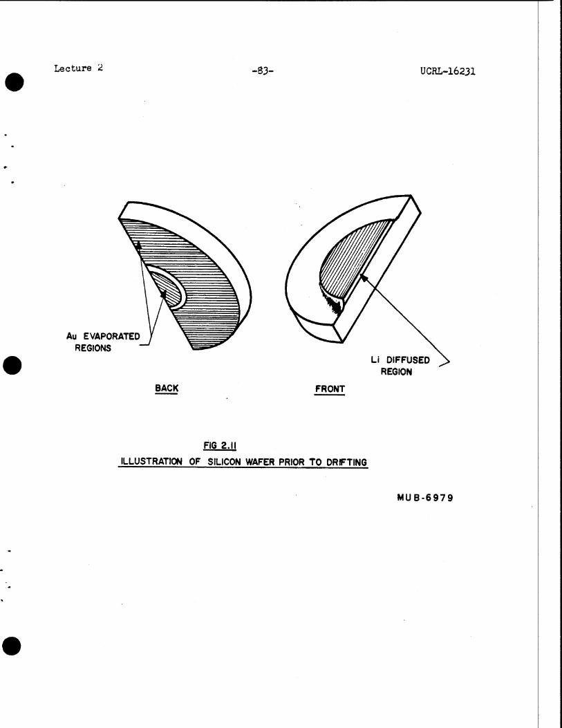


UCRL-16231
LECTURE 3. FACTORS DETERMINING THE ENERGY RESOLUTION IN
MEASUREMENTS WITH SEMICONDUCTOR DETECTORS
Fred S. Goulding
Lawrence Radiation LaboratoryUniversity of CaliforniaBerkeley, California
July 30, 1965
3.1 INTRODUCTION
It is difficult to give a general account of the problems of achieving
high-resolution in semiconductor detector measurements as several inter-
related factors are involved in the final result. In some applications one
set of factors is dominant while an entirely different set may be of crucial
importance in another case. Some of the factors are under the control of
the experimenter (such as counting rate, optimazation of amplifier time
constants, etc.), others are of a semi-fundamental nature (such as vacuum
tube noise) while yet others are truly fundamental in nature (e.g., statistics
of charge production in the detector). In each experiment it is necessary to
appreciate which factors are important and to optimize the parameters accord-
ingly. In this paper we will deal in some detail with the fundamental and
semi-fundamental limitations and in less detail with other factors which may
be encountered. Finally, an effort will be made to indicate types of experi-
ments in which different factors are likely to be important.
In discussing the energy resolution capability of detector systems we
must choose a standard of comparison between them. The standard is always
based upon the equivalent spread in signals at the input to the system but
the particular one employed by a writer often depends whether he is primarily
concerned with designing electronic systems or is concerned with the physical
aspects experiments. In the former case, the signal spread is usually quoted

Lecture 3 -88- UCRL-16231
in terms of the equivalent number of ion pairs corresponding to the signal
spread at the input to the amplifier. To translate this into energy absorb-
tion in the detector, the physicist allows for the value of the average
energy required to produce an ion pair in his particular detector. Most of
the results on preamplifier noise are expressed here in terms of the
equivalent RMS input quoted in ion (or hole-electron) pairs. On the other
hand, the experimental results will be expressed as the full width at half-
maximum of a peak in an energy spectrum (EFWHM). For peaks with a Gaussian
shape this corresponds to about 2.3 times the RMS energy spread. If two or
more sources of uncorelated spread are present their effects must be added
2in quadrature (i.e., ETOTAL =Z+T+1 "2 ......).
3.2 STATISTICAL SPREAD IN THE DETECTOR SIGNAL
If all the energy lost by ionizing particles (or gamma-rays) in a detector
were converted into ionization, signals produced by monochromatic radiation
quanta or particles would show no fluctuations.* On the other hand, if the
energy was mainly dissipated in thermal heating of the lattice and the pro-
bability of an ionizing event was very low compared with that of thermal pro-
cesses, we would expect normal statistical fluctuations in the number of hole-
electron pairs produced. In this case, the RMS fluctuation < n > in the number
of pairs produced would be given by:Ip.
< n > = εv 2(3.1)
where E = energy absorbed by the detector,
ε = average energy required to produce a hole-electron pair.
In semiconductor detectors the situation lies between these two extremes. In
silicon, for example, the yield (i.e., the ratio of the energy used in ioniz-
ing events to the total energy absorbed) is about 1.1:3.6 or about 30%. Fano
*We assume here that the entire particle energy is absorbed in the detectorso that such effects as the Landau collision processes can be neglected.

Lecture 3 -89- UCRL-16231
studied the equivalent situation in gaseous detectors1,2 and the signal spread
is now usually expressed in terms of the Fano factor F. If no is the observed
RMS spread we have:
2-no = F < n >
2(3.2)
In our case, it will be clear from the preceeding discussion that F must be
smaller than unity. Van Roosbroeck has recently performed an elaborate
statistical analysis of the situation. His methods and results are outlined
in the following paragraphs.
A high energy ionizing particle (or the electron produced by a gamma-ray)
produces secondary electrons of lower energy, which produce further lower
energy electrons and so on. Energy losses in this shower process are of three
types:
(a) An electron may impart sufficient energy to an electron in the lattice
to raise it into the conduction band and produce a hole in the lattice.
In this case the original energy is reduced by a small amount equal
to the band-gap of the material and the remainder of the energy is
shared between the degraded incident electron, the secondary electron
and secondary hole. It is usual to assume that the secondary electron
and hole are given equal amounts of energy although this is dependant
upon details of the band structure of the material. The sharing of
energy between the degraded incident electron and the hole-electron
pair can be considered to be random in nature.
(b) An electron travelling through the lattice may lose energy by inter-
actions with the lattice itself. Most of these interactions excite
the lattice in an optical mode of vibration. The energy exchange in
these interactions is quantized and the quanta are characterized by

Lecture 3 -90- UCRL-16231
the Raman frequency of the lattice. For silicon and germanium the
Raman phonon energy is ~ 50 x 10-3 eV and the fact that the ion-
ization yield is only ~ 30% indicates that many optical phonon
collisions take place for each ionizing collision.
(c) The large numbers of very low-energy electrons produced at the
end of the shower process, not having sufficient energy to produce
secondary ionization, must lose the remainder of their energy by
thermal losses to the lattice.
The overall process is shown diagramatically in Fig. 3.1. Using this
model Van Rocsbroeck24 has calculated the curves shown in Fig. 3.2. As the
average energy expended per hole-electron pair finally released is determined
by the same processes as the fluctuations in the number of hole electron pairs,
he has expressed both the yield (i.e., )Energy Gap (Eg)
Average energy per hole electron pair (ε)and the Fano factor as functions of the average number of phonon collisions
per ionizing collision (i.e., r/l-r). If we use the measured values of the
average energy absorbed per hole electron pair we can, by applying Van Roosbroeck's
data, derive a value for the number of phonon collisions per ionizing collision
(~50 for Si, ~90 for Ge) and thence obtain probable values for the Fano
factor (0.28 for Si, 0.36 for Ge).
Unfortunately accurate experimental determination of the Fano factor for
silicon and germanium proves difficult due to several factors. At low energies,
the statistical spread clue to the basic charge production mechanism is usually
small compared with the amplifier noise. This leads to large possible errors
in the determination at low energies. At high energies, many germanium detectors
show poor energy resolution due, we believe, to material non-uniformity. Gamma-
ray measurements at high energies in silicon are difficult due to the very low
efficiency in the photo-peak which makes the measurement doubtful if done with

Lecture 3 -91- UCRL-16231
large activities due to the high counting rate of Compton events and, if done
with small activities, due to amplifier drift, p-particle measurements, on
the other hand, suffer energy loss in the entry window into the detector.
Other complicating factors arise which will not be detailed here. Despite
these difficulties some measurements have been carried out in both silicon
and germanium and the results are consistent with Van Roosbroeck's theory.
A recent set of measurements by Sven Antman and Don Landis in our laboratory
is shown in Fig. 3.3. This shows a plot of the energy resolution (squared)
of a 2 x 1 x 0.8 cm germanium detector as a function of gamma-ray energy.
Great care was taken to eliminate amplifier drift, etc. and the fact that
the points fit well on a straight line indicates that we were dealing with
a purely statistical process. The Fano factor established by these measure-
ments is 0.30 ± 0.03 which is entirely consistent with the approximate value
of 0.32 derived from Van Roosbroeck's curves.
.
3.3 ELECTRICAL NOISE SOURCES
For practical purposes we can assume that all the charge produced in
the detector is collected (i.e., it flows as current in the external circuit).
Therefore, the statistical fluctuations discussed in the previous paragraph
represent the only truly fundamental limits to the energy resolution. However,
several factors prevent our realizing the ultimate resolution in existing
systems. Before outlining these factors it will be useful to discuss a typical
electronic system associated with a semiconductor detector.
Fig. 3.4(A) shows a block diagram of a typical system. The detector supply
voltage is applied through a load resistor, always large in value, so that the
small pulse of charge which flows in the detector in response to the passage
of an ionizing particle will flow into the input of the preamplifier via the
coupling capacitor Cc. After amplification the signal is passed through a
Lecture 3 -92- UCRL-16231
frequency selective filter (often called a pulse shaper) which, in essence,
rejects as much noise while retaining as much signal as possible. A charge
sensitive configuration of the preamplifier as shown in Fig. 3.4(B) is
usually employed as this type of circuit gives an output signal size which,
to a first approximation, is independant of the value of the detector and
stray capacities which appear from its input to ground. This is purely a
matter of convenience and the tradition has grown due to the fact that the
capacity of a junction detector varies as the applied voltage is changed.
The charge sensitive configuration is a little poorer than the conventional
voltage amplifier from the point of view of resolution due to the feedback
capacitor CF behaving as an additional capacity to ground in the equivalent
noise circuit (i.e., a part of CIN in Fig. 3.4(C)).
The equivalent input circuit for studying the energy resolution capabil-
ities of the system is shown in Fig. 3.4(C). The various noise and signal
elements are as follows:
(a) The input signal Q, usually assumed to be a pulse of current of
very short duration compared with the time constants involved in
the system. We will see later that this approximation is not
always valid but will neglect these cases for the moment.
(b) The detector leakage current noise (iN)D. This is assumed to be
pure shot noise which implies that it consists of individual electrons
and holes crossing the depletion layer with no interaction (e.g.,
space charge effects) occurring between the individual carriers.
It arises due to thermal generation of electron-hole pairs in the
depletion layer as expressed in equations 1.13 to 1.15. The mean
square value of the current fluctuations in a leakage current of

Lecture 3 -93-
this nature is given by:-i2 = 2 q · i ∆f.
UCRL-16231
(3.3)
where ∆f is the frequency interval in which the noise is
measured.
(c) The detector series resistance noise (en)RS is due to resistance in
the connections to the sensitive volume of the detector. If the
sheet resistance of the n-type diffusion or the resistance of the
bulk material at the rear of the depletion layer is high this might
be an important source of noise but in well designed detectors it
can be made negligible. We will assume that it is unimportant in
the following discussion. This allows us to simplify the equivalent
circuit by regarding the detector capacity CD and the amplifier input
capacity CIN as being in parallel. We will replace CD + CIN by CT
in the following discussion.
(d) The input current noise (iN)G is due to fluctuations in the input
current to the first amplifying device in the system. If this is a
vacuum tube,it is the sum of the positive and negative grid currents,
assuming that both are present simultaneously. The fluctuations
in this current behave like those in detector leakage current and,
since the two sources in the simplified circuit are in parallel,
we can use equation 3.3 to represent their sum if i = iD + iG.
(e) The parallel resistance noise (en)RL arises from any resistors
shunting the input circuit. This includes the detector load, any
input biasing resistor in the first stage and any resistor included
across CF in a charge sensitive preamplifier. In practice, very
large values are used for these resistors* and we can regard the
time constants used for pulse shaping in the amplifier.
*If RL is the total effective parallel resistance the criterion of interesthere is that the value of the product RL. CT shall be much larger than the

Lecture 3 -94- UCRL-16231
voltage source (en)RL in series with the large resistor RL as a
current source which must also be included in the value of the_
current generator i2 in the previous paragraphs. The increase
in i2 due to this 4 kT ∆f. For this to be negligible we should
_
RL_
make:
(3.4A)
For example, if i = 10-7 A; RL >> 5 x 10⁵ ohm meets the require-
ment. We will assume now that this requirement is satisfied.
(f) The noise developed in the first amplifying device produces a
voltage noise source (en)Req. If this device has adequate gain the
noise due to later amplifier stages is negligible. This source of
noise can be represented by Johnson noise in a resistor and has
the value:
_2en = 4 kT Req ∆f (3.4B)
Where Req is an equivalent input noise resistance in the amplifying
device. In the case of a vacuum tube it is due to fluctuations
in the anode current partially smoothed by the space charge in the
grid-cathode region. Its value is about 2.5_gmfor a triode having a
mutual conductance gm.
Two sources of noise are not shown in Fig. 3.4(C) but must
receive some attention:
(g) Surface leakage currents arising at the periphery of the junction
produce severe low frequency noise in many detectors. The guard-
ring structure and correct surface passivation as described in the
section on diffused detectors in Lecture #2 largely eliminate this
source of noise in many applications. As no adequate theory exists

Lecture 3 -95- UCRL-16231
to explain the details of the behavior of this noise we will
neglect it here.
(h) The plate current of a vacuum tube or other amplifying device shows
fluctuations of a similar nature to those occurring at the surface
of a junction detector. These fluctuations are believed to arise
in processes occurring in the cathode and are dominantly in the low
frequency part of the spectrum.
This source of noise, commonly called "flicker effect" is
usually represented by a noise voltage generator in the input lead
having the value:
(3.4C)
where f is the frequency at which the frequency increment ∆f is
centered and A is a constant (commonly said to be about 10-13).
We can therefore simplify the input circuit for practical purposes to
the one given in Fig. 3.5(A). This can be further simplified to contain only
voltage generators as shown in Fig. 3.5(B). We must now examine the effect
of the amplifier frequency response upon the relative values of signal and
noise at the amplifier output.
3.4 EFFECT OF AMPLIFIER SHAPING NETWORKS
One purpose of the amplifier is the trivial but important one of
amplifying the signal to a level at which it can be used to operate logic
circuits. However, both noise and signal are amplified and frequency dependant
networks must be used to selectively amplify the signals more than the noise.
It will be immediately obvious that a shaping network which results in the
amplifier passing only a narrow range of frequencies will minimize the noise
output power but, unfortunately, it will also reduce the output signal. There-
fore it is reasonable to suppose that the frequency selective network has to be

Lecture 3 -96- UCRL-16231
optimized and the optimum network will depend upon the relative values of
the voltage noise components shown in Fig. 3.5(B). Examination the
noise generators indicates immediately that the noise due to input current
is dominantly low frequency noise, while shot noise in the input element is
more important at high frequencies and flicker noise falls between these
extremes. To determine the actual contributions due to each of these terms
we must evaluate their effect over the full frequency range of the amplifier.
Let F(f) represent the frequency response of the amplifier. The three
contributions to output noise are then:
(a) Shot_ 2EN = 4 kT Req
2
_
(3.5)
(b) Flicker "in+ df (3.6)
(c) Current_
EI = (3.7)
We must now examine typical frequency selective networks to permit evaluation
of the three integrals in (3.5), (3.6) and (3.7). In general, the complete
network will consist of at least one low-pass network (e.g., an RC integrator)
to reduce the shot noise, which would otherwise increase rapidly at high
frequencies, and at least one high-pass network (e.g., an RC differentiator)
which serves to reduce low frequency noise due to input circuit currents.
It will be convenient to express the parameters of the networks in terms of
a normalized frequency fo (and an equivalent time constant to = ). 2 π fo1
Thus, a single RC integrator network of time constant τ, will be represented
by a parameter n, where τ = n τo. The frequency f will be represented by
the parameter m where f = m fo. The gain-frequency function for the RC

Lecture 3 -97- UCRL-16231
integrator shown in Fig. 3.6(A) therefore becomes:
Gain2 = 1 =
1
1 + 4 π2 f2 R2 C2 1 + (nm)2
The gain-frequency function for a number of elements used to build up
shaping networks: expressed in this form, are shown in Fig. 3.6.
In terms of the parameters m and n the equations 3.5, 3.6 and 3.7 can be
rewritten:_EN = 4 kT Req fo 2
?(m1,n1) · F2 (m1,n2) ....) dm (3.8)
EF = A lo?? (F1 (m1,n1) · F2 (m1,n2) ....) ??
m (3.9)
_qi
EI =2
Io. (F1 (m1,n1) · F2 (m1,n2) ...)
m2- dm (3.10)2 π2 CT fo
2
2
_
0
where F1 (m1,n1) represents the frequency response (squared) of the
first element in the shaping network.
F2 (m1,n2) represents the frequency response (squared) of the
second element in the shaping network, etc.
We note now that once a network is chosen (and we assume here that it
is built up of some of the elements shown in Fig. 3.6; elements may be
repeated more than once) the integrals involved in equations (3.8), (3.9) and
(3.10) can be evaluated. We then see that the time scale can be changed
(i.e., fo is changed but n1,n2, etc., remain the same) and only the constants
before the integration signs are affected. Thus the shot noise2 is always
proportional to fo (or inversely to τo), the flicker noise2 is always
*These elements may require a few words of explanation. The RC integratorand RC differentiator require no elaboration. The delay line integrator isa little different from the shorted line frequently employed in amplifiersbut, analytically, it amounts to the same thing. A delayed signal is sub-tracted from the input signal at the input to an operational amplifier stage.The fedback integrator and differentiator are standard operational amplifierconfigurations and, for the purpose of analysis, the open-loop gain of theamplifier is assumed to be infinite.

Lecture 3 -98- UCRL-16231
independant of fo and the input current noise2 is always inversely pro-
portional to fo (or proportional to τo). This is independant of the specific
types of element used in the shaping network.
To illustrate a specific case of equations (3.8), (3.9), and (3.10) we
will look at the shaping network containing a single RC integrator of time
constant τo and a single RC differentiator of time constant to isolated by
a suitable stage τo prevent interaction between the two elements. In this
case equations (3.8), (3.9), and (3.10) become:
2/
Qb
2
EN = 4 kT Req fo
_m2
dmO (1 + m2)2
(3.11)
_2EF = A /
O"m
0 (1 + m2)2dm
_qi 00
EI = 2 s1 dm
2 π2 CT fo 0 (1 + m2)2
These integrals can easily be evaluated analytically and, for this reason,
(3.12)
(3.13)
this case is dealt with in all textbooks. More complex networks containing
several RC integrators, delay line shapers, etc., are analytically quite
unmanageable but the author has recently dealt with a number of such complex
networks by a numerical integration procedure using a computer (see Table 3.1).
The results will be presented shortly.
Hitherto we have concerned ourselves primarily with the effect of these
shaping networks on noise. We must now see what effect they have in the signal.
We mainly interested in the peak height of the output signal as this is the
quantity measured by a pulse-height analyzer. The input signal, as shown in
Fig. 3.5(B), consists, to a first approximation, of a step function of amplitude
The response of a number of typical networks to a unit step function has

Lecture 3 -99- UCRL-16231
been calculated using a digital computer (see Table 3.1) and, for the moment,
we will assume that the output peak pulse height (for unity amplitude input)
is P. Since we are dealing with a linear network the output pulse amplitude
due to the detector signal is then PQ _
CT . In comparing this with the noise we
_must either square the signal or take the square root of the noise2. We will
choose to use the signal squared:
The general equations (3.8), (3.9), and (3.10) can be rewritten:
_EN 4 kT Req CT2 2 _
S2 P2 Q2 = fo ???? (m1,n1) · F2 (m1,n2) ...) dm
???? (m1,n1) · F2 (m1,n2) ...) dm
m
_
=EI qi
J-O”2
S2 2 π2 P2 Q2 fo
_ (F1 (m1,n1) · F2 (m1,n2) ...) dm
_0 m2
(3.14)
(3.15)
(3.16)
It is common to express the noise as the equivalent input noise signal quoted
in ion (or hole-electron) pairs. This implies rewriting equations (3.14),
(3.15) and (3.16) with 1.6 x 10⁻¹⁹ coulombs inserted for Q. To simplify the
presentation we will also substitute I1, I2, and I3 for the three integrals
and will assign values to some of the constants:
(3.17)
(3.18)
(3.19)

Lecture 3 -100- UCRL-16231
We note that the dependance of the three types of noise on the shaping network
is contained in the second terms in parenthesis. The inverse of these ratios,
calculated by a computer for a number of types of netvork, are shown in
Table 3.1. The dependance of noise on the input circuit and on the input
amplifying element is contained in the first terms in parenthesis. The
equivalent shot and flicker noise squared are each proportional to the total
input capacity squared. On the other hand, the equivalent input current noise
squared is independent of the capacity. The overall frequency dependance of
the three types of noise is shown in the terms containing fo.
In Table 3.1 the first four cases involve only RC shaping elements while
the remaining cases use delay-line feedback integrators and simple RC shaping
elements. Comparison of cases #9 and 10 illustrates the worsening of noise
due to double delay-line differentiation. Case #8 is a special one which was
studied mainly from the point of viev of the rather ideal pulse shape it
produces. In all cases, the value in the IP2_ column can be regarded as a figure
of merit of the network for that particular type of noise. Comparing case #5
with case #1 we see that the single delay line with RC integrator is superior
in shot noise ( =P2_ 0.200 as compared with 0.172), flicker noise (0.376 com- I1 -
pared with 0.270) and input current noise (0.34 compared with 0.172.). The useτoof two RC integrators ( )_2 with the delay line (τo) improves shot noise
at a small cost in flicker and input current noise.
However, comparison between networks is not as simple as indicated in
Table 3.1. In many experiments an important factor involved in the choice of
network is the speed of recovery of the shaped waveform to the baseline. This
parameter determines the degree to which pulse pile-up will be a factor at high
counting rates. Fig. 3.7 shows the pulse shapes produced by several of the
networks listed in Table 3.1. We see that, of the cases shown here, the long

Lecture 3 -101- UCRL-16231
tail associated with the RC integrator-differentiator case (#1) is consider-
ably worse than that in the RC integrator-DL differentiator case (#5). The
network #8 is unique among the networks considered here in tha its tail has
completely ended 2.0 µsec after the start of the pulse. Among the more
conventional networks, the double delay line differentiator networks possess
notable advantages at high counting rates. Not only is the tail on the
double delay-line pulse comparatively short but the complete area balance
between positive and negative components of the pulse means that base-line
fluctuations at high rates are small. As seen in cases #9 and #10 of Table 3.1,
however, the price paid for using a double as compared with a single delay line
is an increase in noise.
Another factor influencing the choice between shaping networks is their
sensitivity to input pulse rise-time variations. As will be seen in Lecture 4,
the pulse shape from a practical detector does not have an infinitely short
rise-time and the rise-time depends upon the initial location of the ionization
in the detector. If the maximum collection time is an order of magnitude
smaller than the time constants involved in the shaping network, the effect of
detector rise time variations is negligible but this is not the situation when
using thick silicon and germanium detectors. We have experienced difficulties
in using 3 mm thick silicon detectors for alpha-particles in the energy range
20 - 120 MeV due to the variation of rise-time in the detectors which ranges
from about 100 nsec to 300 nsec depending upon particle energy.* This is in
the same general range as the time constants used in the shaping networks so
that the output amplitude departs from being a linear function of input particle
energy. Moreover, since the particle range is subject to statistical variations,
another source of spread in the amplitude of output signal becomes evident.
In cases where this might happen, the choice of shaping network is influenced
by its sensitivity to input pulse rise-time in addition to the signal to noise
The particles are incident normal to the detector window and therefore theparticle track extends along the lines of electric force.

Lecture 3 -102- UCRL-16231
and counting rate factors discussed earlier. As a general rule, networks
whose output pulse shape has a rounded top (i.e.,_d2V = 0 at Vmax) exhibitdt2
less input pulse shape dependance than networks having a peaked top. It
will be evident from Fig. 3.7 that the single RC integrator delay-line
differentiator #5 (with the delay line length equal to the RC integrator time
constant) is poor in this respect. Using a numerical method the behavior of
several typical networks with regard to input pulse shape sensitivity has
been calculated and the results are given in Table 3.2. This table shows
the percentage loss in pulse height at the output when 40 and 85 MeV alpha-
particles enter a 3 mm silicon detector (at 25°C with 350 V applied to it) as
compared with the pulse height if the detector exhibited an infinitely short
rise time. We note that similar results would be obtained if gamma-rays inter-
acted at various points in the detector.
Examination of Table 3.2 shows, as expected, that the networks which
provide flat-topped pulses perform better with regard to pulse shape sensitiv-
ity. The Table also shows that increasing the time constants of a network to
seperate them further from the input pulse rise time produces a considerable
improvement. However, this increases the input current noise and counting-
rate dependance. The network #9 (which is the same as #8 in Fig. 3.7 and
also #8 in Table 3.1) was designed to produce good input pulse shape dependance
at the same time as good noise and counting rate characteristics. This result
is achieved but the complexity of the arrangement prohibits its general use.
Finally we must note that the fact that the percentage loss figures in Table 3.2
differ for the 40 and 85 MeV particle results in a non-linearity in the energy
calibration of the system. In case #5 this non-linearity amounts to about 2.1%
and had been observed experimentally prior to these computations. A gross
worsening of energy resolution had been observed at the higher energies in these
experiments and both the linearity and resolution effects were largely corrected
by changing to the conditions in Case #8.

Lecture 3 -103- UCRL-16231
3.5 VACUUM TUBES AS THE INPUT AMPLIFYING DEVICE
The optimum choice of vacuum tubes for use as input amplifiers depends
upon the type and properties of the detector being employed. For the purpose
of analysis it is usual to assume that the sources of noise associated with a
vacuum tube are grid current noise (which contributes to the input circuit
noise of equation (3.19)) flicker noise (which contributes to EF in equation
(3.18)) and shot noise (which is responsible for the Req of equation (3.17)).
The grid current and shot noise in a modern vacuum tube are believed to be
well understood theoretically but the flicker effect can differ greatly between
different types of tube and even between individual tubes of one type. There-
fore choice of tube type is made first on the basis of the two best understood
parameters and final selection is usually made by carrying out noise measure-
ments on many samples of the selected types of tubes to determine the amount
of flicker and unexplained noise contributions.
According to Fairstein, the grid current of a triode operated in the normal
mode* is caused primarily by photoelectric emission from the grid due to soft
x-rays produced at the anode by electron bombardment. The grid current is given
approximately by:
Ig = Eg-p IK x 10-10
_
32
where Ig = grid current in amperes,
Eg-p = grid to anode voltage in volts,
IK = cathode current in amperes.
For example, if IK = 12 mA and Eg-p = 100 V; I x 10-9 A.
The grid current of a typical EC-1000 (Phillips) tube operationg under these
conditions is about 2 x 10⁻⁹ A which is in satisfactory agreement with Fairstein's
theory.
It is assumed that the grid bias is large enough to prevent electron collectionat the grid.

Lecture 3 -104- UCRL-16231
It is well known that the equivalent noise resistance of a vacuum tube
triode is approximately equal to 2.5/gm where gm is them utual conductance*
expressed in mhos. However, to prevent very high frequency oscillations in
a vacuum tube it is necessary to insert a grid "stopper" resistance in the
grid lead. This must be added to the tube noise resistance to obtain Req in
equation (3.17). For the EC-1000 tube operated under the conditions of the
previous paragraph and with a 22 ohm grid stopper gm ~16 mA/V and Req = 180 ohms.
It will be clear from the previous two paragraphs that a tube which operates
at a low plate voltage and current will produce a small grid current. However,
this will result in a rather low value of mutual conductance. From equations
(3.17) to (3.19) we see that this means that the vacuum tube will contribute
little noise if long time constants are used in the shaping network (i.e., fo
small) and considerable noise for short time constants. If a detector (such as
lithium-drifted germanium at liquid nitrogen temperature) has very little
leakage current and low capacity, use of an input tube having these character-
istics might make good sense. However, the optimum shaping network would have
a long time constant ( ~5 µsec) and the performance at even moderately high
counting rates performance would be very poor. Moreover, many extraneous
sources of noise such as detector surface noise, microphony in the tube, etc.,
tend to increase at low frequencies. In practice it is usually more satisfactory
to try to work with short time constants in the shaping network and to choose
the tube accordingly.
A high-capacity high-leakage detector calls for a tube having the highest
possible mutual conductance. Its high grid current is of little consequence
since it is swamped by the detector leakage current. In this case the optimum
time constant in the shaping network will be in the 0.5 to 1 µsec region. We
use a 7788 for these purposes.
*If this value is to be put into equation (3.17) T must be assumed to be 300°K.

Lecture 3 -105- UCRL-16231
The preamplifer used in our laboratory for the great majority of high
resolution experiments is shown in Fig. 3.8. As a large amount of data has
been accumulated on this preamplifier we will examine its characteristics in
some detail. The input tube's anode couples to the grounded base stage Q1,
and the collector output of Q1 is emitter followed by Q2. The collector load
of Q1 is bootstrapped from the emitter of Q2 via C1 so that the effective load
presented to the collector of Q1 is almost purely capacitive in the frequency
range of interest. The transistor type used for Q1 and Q2 has very low
collector-base capacity to speed up the response at the collector of Q1 as
much as possible. Feedback to make the input stage charge sensitive is taken
from the emitter of Q2 via RF CF to the grid of the input tube. A 0.5 pF test
capacitor feeds a test signal to the input grid when required and the detector
signal couples via Cc to the same point. The output signals from the charge
sensitive loop feed the feedback amplifier stage containing Q3 and Q4 and their
output feeds a similar stage containing Q5 and Q6. The total gain in these two
stages is 8 but this can be reduced by a factor of 3 by switching S1 to the low
gain position.
Fig. 3.9 shows the behavior of the equivalent noise (squared) for a typical
preamplifier of this type used with equal RC integrator and differentiator in
the shaping network. The plot shows the variation in the mean noise squared as
a function of the shaping network time constant τo ( τo = ) of equations 2 π fo
1
(3.17) to (3.19) ) and as a function of the capacity from input to ground. This
simulates the effect on the resolution of detector capacity.
The full lines in Fig. 3.9 are experimentally measured curves while the
dotted lines are calculated contributions (from equations (3.17) to (3.19))
from the three noise sources for a value of CT = 14 pF. The constant A in the
calculation of flicker effect has been chosen* to produce the best match of the
*The value of A which appears to be applicable to this case is about 7 timeslarger than the generally accepted 10-13. All our experience indicates thatthe generally accepted value is too low.

Lecture 3 -106- UCRL-16231
sum of flicker, shot and grid current noise contributions to the experimentally
measured curve for CT = 14 pF. The match is almost perfect, and, if the noise
contributions are calculated for the other values of CT, equally good agreement
is obtained.
From Fig. 3.9 we note that the resolution of a germanium detector -
preamplifier combination in which the detector has a capacity of 6 pF (i.e.,
CT = 20 pF) and very low (< 10-9 A) leakage is best for a time constant of
1.0 µsec and corresponds to slightly over 2 keV FWHM. This is observed experi-
mentally with good small area detectors. In Fig. 3.10, the effect of a slightly
different shaping network is shown. If we add a second RC integrator equal
in time constant to the first one (and to the differentiator), the energy
resolution for the 6 pF detector becomes optimum at a time constant of 0.5 µsec
and is about 1.85 keV. Also, shown at the right hand side of these curves are
some results for delay-line shaping with two equal RC integrators. We see
that the 6 pF detector case gives a little less than 1.8 keV. On the other
hand, we note that, due to the short time constant (0.8 µsec) of the delay-line
differentiator, the performance of the delay-line system is worse than the RC
system (at its optimum point) when higher capacity detectors are used.
A convincing illustration of the validity of the theoretical model is
shown in the comparison between Figs. 3.10 and 3.11. The only difference between
the cases shown in these two figures is that the shunt input resistance (RF in
shunt with RL) is 60 M ohm in Fig. 3.10 and 500 M ohm in Fig. 3.11. This
should theoretically (see section 3.3(e)) change the effective value of the
grid current by 0.8 nA. The improvement at long time constants in Fig. 3.11
is close to this value. The improvement in resolution for the 6 pF detector
case is significant (now 1.7 keV).

Lecture 3 -107- UCRL-16231
For future reference in discussing some of the fast timing possibilities
of detectors, the rise time behavior of this preamplifier is shown in Fig. 3.12.
However, it should be remembered that, if a fast amplifier is used to amplify
the signals from the preamplifier, the noise levels, instead of being those
shown in Figs. 3.9 and 3.10, are determined by the time constants in the fast
amplifier. If it contains a differentiator - integrator combination of 10 nsec
time constant the energy resolution with a 12 pF detector will be in the region
of 15 keV FWHM.
3.5 ALTERNATIVE LOW NOISE AMPLIFYING ELEMENTS
Particularly for low-energy gamma-ray measurements, the energy resolving
capability of a semiconductor detector spectrometer is determined at the present
time by the electrical noise properties of vacuum tubes. While minor improve-
ments (e.g., higher gm and reduced igand capacity) in vacuum tube character-
istics can be anticipated it seems unlikely that radical improvements will.
arise in this area. It is natural, therefore, to inquire into the possibility
of obtaining better performance by using techniques not based upon vacuum tubes.
Ultimately we might hope that the energy resolution will be determined solely
by the statistical process described in section 3.2 and, to accomplish this,
we look for an improvement of about 5:1 in the electronic resolution of these
systems.
A little work has been done on the use of a parametric amplifier system
(Chase and Radeka) and some promising results have been obtained. However,
parametric amplifiers are much more complex than our normal amplifiers in
requiring the use of a very high frequency radio frequency carrier. As a
consequence the behavior of such systems is difficult to analyze and, moreover,
obtaining the ultimate performance depends upon critical aajustment of parameters.
Probably for these reasons, no significant results have yet been published on
systems of this type.

Lecture 3 -108- UCRL-16231
A more promising alternative at the present time seems to be the use of
a bulk* field-effect transistor. The operation of this device is illustrated
in Fig. 3.13 which shows a source and drain electrode connected by an n-type
"channel" which is partially "pinched off" by the depletion layer produced
by a reverse biased "p" region diffused into the side of the n-type channel.
(Note that p-type channel devices are also available.) From our previous
discussion it will be obvious that increasing the negative bias on the gate
electrode of Fig. 3.13 causes the thickness of the conducting channel to be
reduced thereby modulating its impedance. Moreover we note that the impedance
seen looking into the gate electrode is very large - being that of a reverse
biased diode. Due to the voltage drop along the length L of the channel the
junction is reverse biased to a greater extent near the drain electrode and
the voltage distribution along its length has the general form shown in
Fig. 3.13. We will only discuss certain aspects of the theory of field-effect
transistors here but the behavior of the device is well understood and has
been thoroughly analyzed.
For some time we have been using field-effect transistors of this type
in a general purpose preamplifier not used for very high resolution work.
Fig. 3.14 shows the circuit of this unit and will be used to illustrate the
mode of use of a field-effect transistor before we examine some of its noise
characteristics, which are of major importance to us in high resolution spec-
trometry. Comparing this unit with the vacuum tube preamplifier we see that
the basic configuration of the input charge sensitive stage containing Q1, Q2,
Q3 and Q4 is similar to that of the stage containing input tube, Q1, and Q2
in Fig. 3.8. However, due to the low voltages required for the field effect
transistor we are able to conveniently D.C. couple the complete loop. Also,
*We have delibertely used the word bulk to discriminate between this type of fieldeffect transistor in which control of carriers takes place in the bulk materialand the type (MOS) in which the conductivity of a surface layer under an oxide ismodulated. Since conduction in a surface layer will most likely be noisy (thisis confirmed by experiment) we will neglect the MOS type of transistor in thisdiscussion.

Lecture 3 -109- UCRL-16231
owing to the rather low mutual conductance (4 mA/V) of the field-effect
transistor, we have found it necessary to use a White emitter-follower Q3,
Q4 within the feedback loop to raise its gain and thereby improve the rise
time. Only a single gain stage is used at the output of this preamplifier;
this is due to the particular area of use aimed for in the design. We should
note two features concerning the input circuit of this preamplifier. The
diode CR1 is provided to protect the transistor against high voltage surges
introduced when switching detector voltage on or off. The adjustable feed-
back and test capacitor arrangements are used to align many preamplifiers
to have the same energy calibration and, in fact, in the particular installation
using these preamplifiers, a Helical potentiometer pulser dial is calibrated
directly in MeV (100 MeV = 1 V into the test capacitor).
According to the analysis of Van der Ziel,25,26 the noise introduced by
a field-effect transistor is due simply to resistance noise occurring in seg-
ments of the conducting channel. A noise voltage developed in a small element
of the channel modulates its width and thereby affects the channel conductance.
Also, the noise modulation of the depletion layer width causes a noise current
to flow in the gate electrode circuit. These effects can conveniently be
expressed for all practical purposes in an equivalent noise resistance Req
given by:
(3.20)
where CT is the total input shunt capacity (as always).
Cgs is the gate-source capacitance of the FET.
Equations (3.17) to (3.19) are still valid for this case, where Req in equation
(3.17) is assigned the value calculated from equation (3.20); constant A in
equation (3.18) is the flicker noise constant (not known for FET's but probably
quite variable from unit to unit due to surface effects at the edge of the
junction); i is the gate junction leakage current.

Lecture 3 -110- UCRL-16231
In choosing a field-effect transistor for use as an input amplifying
element the same considerations apply as in the vacuum tube case. Since, in
most practical situations detector leakage current noise and surface noise
cause noise at long time constants, the objective should be to design for an
optimum shaping network with a time constant close to 1 µsec. This places
emphasis on keeping Req small and, therefore, gm large. Commercial units are
available in the range 2 mA/V to 20 mA/V and these justify examination.*
Assuming a slightly worse value of Req than equation (3.20) would indicate
and a typical total capacity of 20 pF, Fig. 3.15 shows the noise behavior
predicted for gate junction leakage current noise (assuming 10-9 A which is
typical) and for channel noise for different values of gm for room temperature
operation. We have shown no flicker noise contribution in these curves but
recognize that, in practice, such a contribution may be dominant. For a
transistor having a gm of 5 mA/V and ig = 10-9 A the FWHM resolution indicated
by Fig. 3.15 is 1.6 keV with an optimum time constant of 2 µsec. If the mutual
conductance is 10 mA/V the optimum moves to 1.3 µsec and the resolution becomes
1.3 keV.
While recognizing that practical devices rarely agree precisely with
theory, it is extremely promising when theory predicts such attractive results.
However the situation improves still further when we look at the theoretical
behavior at liquid nitrogen temperature. At low temperatures one might expect
flicker noise to disappear** and this removes an important unknown trom the
theory. Moreover, in equation (3.17) we note that the absolute tempearture T
*We note that, if CT = Cgs (i.e., no added capacity) then Req < 1/gm. This isto be compared with 2.5/gm for a triode, a 2.5:1 improvement for the same gm.On the other hand, a low gm in the first amplifying element may cause noisein the second element to become important.
**One can argue that we see no flicker noise in very large area germanium detectorsat 77°K and, therefore, can expect even less from the minute field-effectdevice gate junction.

Lecture 3 -111- UCRL-16231
appears and, unlike the vacuum tube case, we can use low temperatures to
reduce this source of noise. Furthermore, the gate junction leakage current
fails practically to zero and input current noise will be solely that due to
generation of carriers in the bulk of the detector, Fig. 3.16 shows the
predicted behavior of channel noise and input current noise at 77°K. We see
that a gm of 10 mA/V and detector leakage of 2 x 10⁻¹⁰ A gives optimum
resolution of 0.6 keV at 1.5 µsec time constant.
It is interesting to note that it is, in principle, very simple to make
high mutual conductance field-effect transistors for operation at liquid
nitrogen temperature. Since, at this temperature, the donors (or acceptors
except indium) are fully ionized, the behavior of the depletion layer as a
function of gate voltage is unchanged as compared with room temperature oper-
ation. However, the channel conductivity in good material will be ~30 times
larger at 77°K than at 300°K due to the increase in carrier mobility. Both
the gm and the device current will increase by this factor. If the power
dissipated by the device can be removed while maintaining it close to 77°K a
high value of gm should be available. Alternatively, if the current is main-
tained constant while cooling the device, the depletion layer adjusts itself
to thin down the channel and the gate-source capacitance is reduced --
another desirable result.
Measurements of commercial device parameters at low temperatures prove
to be disappointing. Nearly all these devices are manufactured with a highly-
doped poor quality epitaxial channel and impurity scattering limits the improve-
ment in gm to a factor of about 3 as compared with room temperature operation.
Moreover, one suspects that the impurity scattering and trapping processes in
the channel introduce aacitional noise sources. Due to this we are in the
process of making our own FET using materials and techniques similar to those

Lecture 3 -112- UCRL-16231
employed in diffused detectors. However, with all their drawbacks, commercial
field-effect transistors do perform as reasonably low-noise amplifiers and
we present here some measurements on these devices.
The circuits used in these measurements are shown in Fig. 3.17. The upper
circuit is used for testing n-channel devices while the lower one tests p-
channel units. The designs are similar to that of Fig. 3.14 and employ the
same output stage. Choice of resistor R in Fig. 3.17 permits adjustment of
the current in the field-effect transistor over a wide range. In interpreting
the results to be presented here, the fact that only a small number of samples
were tested should be borne in mind. This may explain the apparently inferior
27,28results compared with those given in two published papers. However, the results
given here do represent nearly the best obtained from a lengthy investigation of
several promising types of commercial field-effect transistors.
Fig. 3.18 shows performance curves for a p-channel unit (TIS-05) made by
Texas Instruments. This transistor has an effective gate-source capacitance of
about 10 pF and a mutual conductance at 25°C of 4 mA/V. In these tests it was
operated with a source-drain voltage of 4.5 volts. Three samples were tested,
all gave virtually the same results. Previous tests had shown that the con-
ductance of the channel increased by a factor of three at the lower test temper-
ature (about -160°C) as compared with room temperature. Consequently the low
temperature test was carried out at a drain current of 15 mA while the room
temperature test was at 5 mA.
For this type of transistor we note that a large flicker noise contribution
is present at room temperature as indicated by the flatness of the curves. We_
also see that the value of N2 at low temperatures is almost an order of magni-
tude higher than would be predicted from Fig. 3.16. However, at time constants
greater than 1 µsec the low temperature performance of this type of unit is
better than the results obtained with the EC-1000 for the low capacity conditions.

these extra sources of noise is best illustrated by the fact that our tests
on some samples of one type of transistor show that its noise level increases
as the temperature is reduced. There is good evidence that a field-effect
transistor made with good material will come close to theoretical predicted
performance.
Lecture 3 -113- UCRL-16231
Fig. 3.19 shows the results of a similar set of measurements on the
Amelco 2N3458. We note again that the results for N2 are almost an order
of magnitude larger than predicted despite the fact that these units are
apparently largely free of flicker noise. The higher gate source capacity
of these units partially accounts for the results on the Amelco device
being worse than those on the TI unit.
In conclusion it might be said that commercial field-effect transistors
made by the epitaxial process almost equal the best vacuum tube performance
in low noise preamplifiers but unexplained sources of noise prevent them
approaching their theoretical possibilities. The lack of understanding of
3.7 ADDITIONAL SOURCES OF SIGNAL AMPLITUDE SPREAD
The previous sections have been-concerned with rather fundamental sources
of spread in the amplitude of signals. However, it is frequently the case that,
due to the nature of the experiment or due to inadequate appreciation of the
problems on the part of the experimenter, the forementioned sources of signal
spread are swamped by other problems. We will briefly discuss a few of these
problems here.
3.7.1 Noise Contribution of Main Amplifier.
Nearly all amplifier systems contain a signal attenuator to permit oper-
ation with large input signals as well as small ones. This usually appears
between the preamplifier and the first amplifying stage of the main amplifier.

Lecture 3 -114- UCRL-16231
If large signals are produced at the input to the preamplifier, the attenuation
must be increased to maintain the amplifier in its linear working range. This
is always the case when dealing with high energy reactions using silicon
detectors. In these cases one must be careful to avoid the noise in the first
amplifying stage of the main amplifier becoming dominant. For this reason it
is usually necessary to provide a further gain attenuator switch located later
in the amplifying chain and this should be turned to its lowest gain
position before attenuating at the input to the main amplifier.
3.7.2 Gain Drifts
In high resolution spectroscopy using semiconductor detectors one is
frequently working with a spread in the amplitude of pulses equal to about
0.1% of their value. Gain drifts in amplifying systems over a period of a few
hours may well be in the region of this same percentage. The experimenter
must use either a very stable amplifier or one equipped with an overall gain
stabilization servo system if he is to use the true potential resolution of
semiconductor detector systems. This is particularly true when using silicon
detectors for high energy nuclear reaction studies in the 10 to 100 MeV range
and in the case of measurements of high energy gamma-rays ( ~ 1 MeV or greater)
with germanium detectors.
3.7.3 High Counting Rates
At high counting rates pulse pile-up and baseline fluctuations may cause
serious signal spread. It is a good rule to anticipate trouble from this
source if the counting rate is higher than p/τo, where p is the fractional
resolution in the detector amplifier system. Thus if p = 0.3% and τo = 1 µsec,
one begins to detect rate effects at about 3 kc/s. The counting rate at which
these effects appear can be increased by an order of magnitude or more by using

Lecture 3 -115- UCRL-16231
double delay-line or double RC differentiation but use of this type of shaping
network causes a loss of resolution at low counting rates (compare cases #9
and #10 of Table 3.1).
3.7.4 Finite Detector Pulse Rise Time
Since the detector pulse shape is a function of the position of formation
of ionization in the detector, a spread in detector pulse shape results in
many detector applications. If the detector pulse rise time is within a factor
of 5 of the value of to used in the shaping networks, a spread in signal
amplitude at the output of the amplifier can be anticipated. Table 3.2 gives
some guidance toward choice of network in these cases and the section dealing
with detector pulse shape in Lecture #4 also presents some information relevant
to this situation.

Lecture 3 -116- UCRL-16231
Table 3.1. Noise Integral and Peak Response of Several Networks
PEAKOUTPUT (P)
NETWORK DESCRIPTION (UNITY INPUT)
1. RC INTEG (τo) .368 .784 .172 .500 .270 .785 .172+RC DIFF (τo)
2. TWO RC INTEG (τo) .271 .196 .372 .250 .292 .589 .124+RC DIFF (τo)
3. THREE RC INTEG (τo/2) .356 .407 .310 .421 .300 .771 .163+RC DIFF (τo)
4. RC INTEG (τo)TWO RC INTEG (τo/2) .295 .233 .373 .290 .300 .640 .136RC DIFF (τo)
5. RC INTEG (τo) .628 1.98 .200 1.05 .376 1.16 .341D.L. DIFF (τo)
6. TWO RC INTEG (τo/2) .631 1.87 .214 1.20 .333 1.32 .303D.L. DIFF (τo)
7. RC INTEG (τo)TWO RC INTEG (τo/2) .388 .494 .303 .481 .312 .823 .182D.L. DIFF
8. TWO F.B. INTEG (τo)TWO D.L. DIFF (τo) 1.000 4.19 .239 3.61 .277 4.82 .208TWO D.L. DIFF (2 τo)
9. RC INTEG (0.4 τo) 0.981 7.70 .125 3.77 .254 3.79 .253 D.L. DIFF (1.6 τo)
10. RC INTEG (0.4 τo) 0.981 23.0 .042 9.82 .098 6.37 .151TWO D.L. DIFF (1.6 τo)

Lecture 3 -117- UCRL-16231
Table 3.2. Input Pulse Shape Dependance of Several Shaping Networks
(3 mm Li-drift Si detector at 350 V and 25°C)
PERCENTAGE LOSS FOR PERCENTAGE LOSS FOR40 MeV ALPHAS 85 MeV Alphas
1. RC INTEG (0.5 µsec) 0.46 1.73 RC DIFF (0.5 µsec)
2. RC INTEG (1.0 µsec) 0.11 0.41RC DIFF (1.0 µsec)
3. THREE RC INTEG (0.2 µsec) 0.54 1.96RC DIFF (0.5 µsec)
4. THREE RC INTEG (0.2 µsec) 0.99 3.01D.L. DIFF (0.8 µsec)
5. RC INTEG (0.5 µsec) 3.11 5.22D.L. DIFF (0.8 µsec)
6. RC INTEG (0.5 µsec) 3.59 5.74TWO D.L. DIFF (0.8 µsec)
7. RC INTEG (0.2 µsec) 0.89 1.63D.L. DIFF (0.8 µsec)
8. RC INTEG (0.5 µsec) 0.95 1.51D.L. DIFF (1.4 µsec)
9. TWO F.B. INTEG (0.5 µsec) TWO D.L. DIFF (0.5 µsec) 0.46 1.57D.L. DIFF (1.0 µsec)

Fig. 3.1 Diagramatic Representation of Energy Loss Process.
Fig. 3.2 Calculated Yield and Fano Factor.
Fig. 3.3 Resolution-Energy Relationship Data for Germanium.
Fig. 3.4 Typical Electronics for Spectroscopy.
Fig. 3.5 Simplified Input Equivalent Circuits.
Fig. 3.6 Typical Shaping Networks and Their Frequency Response.
Fig. 3.7 Pulse Response of Several Networks (Unit Function Input).
Fig. 3.8 EC-1000 Preamplifier.
Fig. 3.9 Noise Performance Curves for EC-1000 Preamplifier.
Fig. 3.10 EC-1000 Preamplifier: Effect of Double Integrator.
Fig. 3.11 EC-1000 Preamplifier. (Conditions as in Fig. 3.10 except
Fig. 3.12 EC-1000 Preamplifier Rise Time Curves.
Fig. 3.13 Bulk Field Effect Transistor (N-Channel Type Illustrated).
Fig. 3.14 General Purpose Field Effect Transistor Preamplifier.
Fig. 3.15 Predicted Noise Behavior of Field Effect Transistor at 300°K.
Fig. 3.16 Predicted Noise Behavior of Field Effect Transistor at 77°K.
Fig. 3.17 Circuit for Low Temperature Tests on Field Effect Transistors.
Fig. 3.18 Noise Performance of TIS-05 Field Effect Transistor.
Fig. 3.19 Noise Performance of Amelco 2N3458 Field Effect Transistor.
-118- UCRL-16231
LECTURE 3. FIGURE CAPTIONS
[ ]er = Raman Phonon Energy for Lattice.
eg = Band-Cap of Materialp Assumes a Random Value in the Range 0 to 1.
(RF = 60 M Ω)
RF = 500 M Ω)
(2N3458 at Room Temperature.)
CT = 20 pF; Req = 1/gm Assumed
CT = 20 pF; Req = 1/gm Assumed
Conditions: See Text; Dotted Lines: -170°CFull Lines: + 25°C
Conditions: Dotted lines: -170°C ID = 12.5 mAFull lines: + 25°C ID = 5 mA


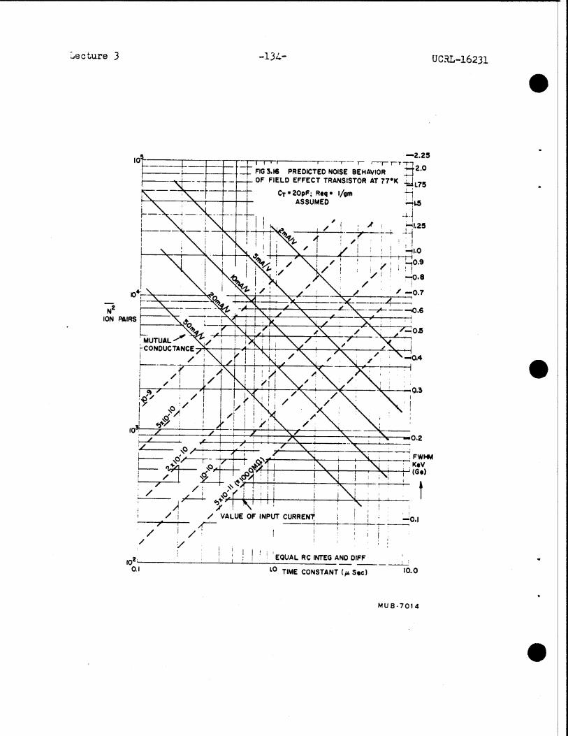


-138- UCRL-16231
LECTURE 4. MISCELLANEOUS DETECTOR TOPICS
Fred S. Goulding
Lawrence Radiation LaboratoryUniversity of CaliforniaBerkeley, California
July 30, 1965
4.1 DETECTOR PULSE SHAPE
The passage of an ionizing particle or the interaction of a gamma-ray in
the sensitive region of a detector releases a large number of hole-electron
pairs which are separated and collected by the electric field present in the
depleted region. The initial spatial distribution of the hole-electron pairs
depends upon the type and energy of the radiation and, therefore, the shape of
the current pulse obtained from the detector is changed by the same factors.
It is also determined by the thickness of the sensitive region, by the electric
field distribution within this region and by the mobilities of the charge
carriers in the semiconductor at its operating temperature. The interrelation
between these factors makes a general solution to the calculations of pulse
shape quite impossible. We will therefore content ourselves with discussing
some of the basic considerations and giving some examples of solutions for
particular cases. It is instructive to first consider the signal resulting
from creation of a single hole-electron pair in the sensitive volume. As the
result is different for p-i-n detectors, in which the electric field is constant
through the whole sensitive region, from that for p-n junctions, in which the
field is a linear function of distance from the back of the depletion layer,
we will deal with these two cases separately.

Lecture 4 UCRL-16231
4.1.1 Pulse Shape Due to a Single Hole-Electron Pair in a P-I-N Detector
We will consider the situation depicted in Fig. 4.1. The parameters shown
in this figure are self-explanatory and will be used here. We will assume that
the detector is connected to a charge sensitive preamplifier with a feedback
capacitor CF and an open loop gain -A, which is very large. Any chrage flowing
in the detector tends to produce a negative signal et the input to the amplifier
but the feedback via CF forces the amplifier input point (and therefore the
detector anode) to stay almost at constant potential. The simplest way to
calculate the signal is to consider the energy balance in the system. Thus,
as the carriers are collected by the electric field in the detector, energy is
dissipated* and, to maintain the energy stored in the detector dielectric, a
charge must flow into the positive side of the detector from the external
circuit. This charge flows almost entirely out of CF giving a negative output
signal from the amplifier.
We have:
1 Q2Energy W stored in the dielectric = 2 C
__
where Q = charge on the detector capacity C.
...
...
V2Also work done on the electron in time dt = Force X Distance = · q · µe.
_ _
_W2
From this:
dW V2 = · q · µedt W2
= Q2 · q· µe
W2C2_
Q dQC dt W2C2
= Q2 · q µe
i.e., dQ V= · q · µe
_ _ _
_ _dt W2
*This energy appears as thermal vibrations in the lattice due to theelectron wave interacting with the lattice.

Lecture 4 -140- UCRL-16231
This is the current ie in the external circuit.
W2V _ .
.. ie = · q · µe (4.1)
This current persists until the electron reaches the positive plate when
it suddenly becomes zero. The time Te taken for this to happen is given by:
_ _ µe V
Te = W-xo W
(4.2)
Similar equations can be derived for the signal due to hole flow:
Vih = · q µh
_
W2
W
(4.3)
Th = ·xo_ _µh V
(4.4)
The total charge flow in the external circuit is given by:
QTOTAL =
= q.
While this is anticipated, the author must comment that many beginners in this
field find it difficult to believe that the total charge flow is not 2 q.
We note that the output signal is the integrated value of i flowing in
the capacitor CF. The resulting output signal due to the hole-electron pair
is shown in Fig. 4.2 (the signal is inverted for convenience). The two compon-
ents of the signal are shown and it will be obvious from this diagram that,
for this type of detector, the signal due to either type of carrier is pro-
portional to the fraction of the sensitive region crossed by that carrier.
This simple situation results from the fact that the net charge residing in
the sensitive region is zero end, therefore, the electric field is constant.
We will shortly see that the situation is more complicated in the case of the

Lecture 4 -141- UCRL-16231
p-n junction detector. A complication arises in the foregoing analysis (and
for p-n junction detectors) if the electric field is large enough to produce
carrier velocities in the same range as thermal velocities of electrons in
the lattice. This is about 107 cm/sec. In germanium, the velocity of an
electron moving through the lattice is limited to about 107 cm/sec.16 and a
similar, though not so abrupt, limiting velocity exists for holes. In silicon,
the velocity of carriers does not saturate as in germanium but the mobility
falls fairly rapidly when carrier velocities reach the region of 107 cm/sec.
This limitation is of some significance when considering very fast timing
with thin (silicon) detectors and also when dealing with the case of germanium
detectors used at 77°K. The high mobility of carriers in germanium at this
temperature means that the saturation velocity is reached for electric fields
in the 1000 V/cm range. This is not an unusual field in germanium detectors
and the previous analysis must be applied with care to this case.
4.1.2 Pulse Shape Due to a Single Hole-Electron Pair in a p-n Junction Detector.
Fig. 4.3 depicts the situation here. The electric field is a linear
function of distance from the bask of the depletion layer. Again we will con-
sider the energy balance equations.
We have:_ _= ·_dWe Qdt C dt
dQe
For the electron:
W22V_ = E(x) µe = · x · µe
dx _dt
2 V µe t_W2
... x = xo e (4.5)

Lecture 4 -142- UCRL-16231
The work done on the electron in time dt:
( )= 4 V2
· q µe x2 dt
dt W4
_
= E(x) 2 · q · µe dt
W4
dWe_ _
... =
4 V2 · q · µe · x
2.?? ??? ???
Equating the two expressions for dWe/dt we have:
= ie = 4 V · q · µe x
2dQe _ _ W4dt
Substituting from (4.5):
4 V · q · µe xo 2 _ 4 µe · V · t
ie = W2
W4 e
The total charge flow due to electrons is therefore:
(4.6)
J-t
Qe = 0
ie dt
(4.7)
The electron is collected after a time Te given by:
W2Te = loge ( )
2 V µe
_Wxo
Substituting in (4.7), the total charge Qeo due to the electron is given by:
Qeo =
(4.9)

Lecture 4 -143- UCRL-16231
For the hole we have:
Also,
dxdt
= E (x ph = - · x · µh)_
dQdt_ = ih = · q · µh x
2_W4 4 V
... ih =
4 V · q · µh · xo _
e W2
W4
2
tih dt.
1 - e
(4.10)
(4.11)
(4.12)
Equation (4.12) shows that the hole collection waveform is a negative
exponential and requires an infinite time to be completed. The time constant
2 VW2
We have
_
Total charge due to hole = Qho = o_
W2 (4.13)
... Total charge (electrons + holes) = q
This is expected.
Fig. 4.4 shows the pulse shape which is produced. We see that this is
much more complicated than the p-i-n detector case and practical use of these

Lecture 4 -144- UCRL-16231
equations is very limited. However, it is interesting to calculate the time
constantW2
4 V · µh for a silicon detector made from p-type material.
We have:
W = 0.33 ex 10-4 µh * 500 cm
2/V sec.
... Hole collection time constant = x 10-9 sec_
ρ
2000ρ= n sec _
2000 (4.14)
If ρ = 1000 Ω cm
Hole T.C. = 0.5 nsec.
The electron component in the output signal is much faster than this. These
results indicate the possible uses of such detetors for fast timing applications.
The very fast apparent charge collection time in a p-n junction detector
introduces the possibility that other factors limit the rise time of the
output signal. For example, the dense plasma of holes and electrons produced
by a heavily ionizing particle must be eroded away partly by self-diffusion
before the holes and electrons can be considered to be moving under the influ-
ence of the applied electric field. The significance of this is indicated by
the fact that a fission fragment track might contain 1018 hole-electron pairs
per cm3 immediately after its formation and this is about five orders of magni-
tude higher than the equilibrium density of acceptors in the material. A
similar situation, though not so exaggerated, exists for alpha particles. It
is very likely that the ultimate timing possibilities of such semiconductor
detectors will be limited by factors like this but insufficient evidence exists
at the present time to determine the limit set by plasma erosion.
Another degradation of output signal occurs due to the series R, shunt
capacity time constant of the detector. If the detector is made with good

Lecture 4 -145- UCRL-16231
low sheet resistance n+ and p+ layers on front and back and is operated
in a punched-through mode this is not an important factor.* However, if
the detector volume is only partly depleted, the series resistance of the
undepleted bulk may be a serious factor in limiting the speed. As an
illustration we might consider a detector made with 500 Ω cm silicon
(p-type) on a wafer thickness of 500 microns but depleted only to a depth
of 100 microns. If the detector is of 1 cm2 area, its capacity will be
about 100 pF and the resistance of the 400 microns of undepleted bulk
material will be 20 ohms. The resulting RC time constant is 2 nsec. The
time constant for hole-collection in this detector is only 0.25 nsec -
showing that rise time in a case like this may be limited by the combination
of detector capacity and series resistance.
Two further possible limitations can be discussed using the example
of the previous paragraph. We will suppose now that the wafer had been
thinner so that the undepleted bulk was negligible. It is necessary to
apply 200 Volts to this detector to deplete 100 microns. The peak electric
field is 4 x 10⁴ V/cm and, assuming a hole mobility of 500 cm2/V sec., the
hole velocity should reach 2 x 107 cm/sec. We note that the peak field is
in the range where junction non-uniformity may cause small avalanching
effects (called microplasma) making the device noisy. Moreover, the calcu-
lated hole velocity is larger than the 107 cm/sec at which the mobility
falls off. The result of this is to slow down the hole collection somewhat.
However, the effect is a minor one as the holes spend most of their time
in the regions of lower electric field where normal mobility may be assumed.
For very fast timing purposes a punch-through device made on high resis-tivity material is best. By applying a large over-voltage the electricfield becomes constant across the device. We note that a carrier travelingat 2 x 107 cm/sec (a good value for the saturation velocity) crosses a25 micron region in 0.1 nsec.

Lecture 4 -146- UCRL-16231
We see that the pulse shape obtained by collection of a single hole-
electron pair in a p-n junction detector is quite complex and, moreover,
the collection times are so short in thin sensitive regions that secondary
effects often determine the output pulse shape. There is therefore little
point in extending the topic of p-n junction detectors to deal with the
complications which arise when collecting a track of ionization. However,
the problem is more manageable and important in the p-i-n detector and we
will now examine it for some types of radiation.
4.1.3 Pulse Shape Distribution for Gamma-rays in Germanium P-I-N
Detectors at 77°K.
Gamma-rays in the energy range of commonest interest may be considered
to possess a low probability of interacting in a germanium detector. More-
over, if the detector's linear dimensions are about 1 cm, the range of the
electrons produced by the gamma-ray is small compared with the sensitive
thickness of the detector (at 1 MeV the electron range in germanium is less
than 1 mm). Therefore we may consider gamma-rays in this energy range to
produce a uniform distribution of events in the detector volume and the
ionization due to each event to be localized at a point. These arguments
must not be applied to the case of low-energy gamma-rays where the absorb-
tion in the front region shields the beck regions giving a non-uniform event
distribution, nor can they be applied to very high-energy gamma-rays where
the range of electrons produced by the gamma-rays is a large fraction of the
detector dimensions. These restrictions limit the validity of this discuss-
ion to the energy range of about 100 keV to 2 MeV.
Since we can now regard the ionization produced by an interaction as
being localized at a point, a pulse shape like that in Fig. 4.2 will apply

Lecture 4 -147- UCRL-16231
to a single event uith the vertical scale being multiplied by the ratio
E/ε. The relative electron and hole contributions to the total signal
will depend upon the exact location of the event in the detector. How-
ever, in Fig. 4.2 the hole mobility was assumed to be much smaller than
the electron mobility. As seen in Fig. 1.2, the calculated hole mobility
at 77°K is slightly higher than the calculated electron mobility. In
practice, due to the velocity saturation phenomena in germanium at field
strengths in excess of 1000 V/cm (which is commonly used for detectors),
it appears that one can assume that both carriers travel at 1.5 x 10⁷ cms/sec.*
Therefore, if an ionizing event occurs at distance xo from the negative
electrode the range of pulse shapes will be as shown in Fig. 4.5. We
note that the fastest pulse occurs when the event is at the middle of the
sensitive region. Moreover, since we are assuming an equal probability of
an event occuring at any position, pulse shapes in the range shown in
Fig. 4.5 are equally probable.
The spread in pulse shape indicated by Fig. 4.5 has two possible con-
sequences. From the point of view of energy measurements, it may cause
a spread in pulse height following the shaping network of the amplifier
(see section 3.4). Present limitations on the thickness of germanium
detectors ( ~ 1 cm) which limits the maximum collection time to aoout
60 nsec and use of typical shaping network time constants in the 1 psec
region have made this an unimportant ractor up to the present time. How-
ever, as thicker detectors are developed it may become significant and,
if so, the effect (which is amenable to calculation) will influence the
choice of optimum shaping network. A more important consequence of the
spread in pulse shape, at the present time, is its effect on the fast
*This value appears to be the best fit to data we have obtained as wellas being close to that measured by Prior.16

Lecture 4 -148-
timing possibilities of germanium detectors. Here a timing pulse is
obtained when the pulse crosses a fixed threshold level. The relative
probability of the delay between the gamma-ray and the timing pulse
having a value t is easy to calculate for the shape distribution of
Fig. 4.5 and is shown in Fig. 4.6. Here the factor β is the setting
of the threshold pulse discriminator expressed as a fraction of the
total pulse height. We see that the distribution of time delays is
characterized by a sharp peak obtained from events in the central region
of the detector and a flat distribution due to the events in the outer
regions. In most practical. applications a range of gamma-ray energies
occurs resulting in a further time spread. However, we have used 3 mm
thick germanium detectors observing two gamma-ray lines (70 and 80 keV)
with a fast coincidence resolving time between the detectors of less
than 5 nsec (FWHM).
In the foregoing discussion we have made the assumption that the
sensitive region of the detector was completely intrinsic so the electric
field was constant through the whole volume. If this is not true, further
time spread may occur. In practice many detectors appear to contain sub-
stantial regions which are poorly compensated.* These regions cause many
very slow pulses which degrade energy spectra as well as coincidence
resolution. T. K. Alexander17 has used a shape discrimination system to
eliminate these slow pulses.
We tend to attribute this to the presence of impurities such as iron,nickel, etc. in germanium. The lithium compensates the acceptors dueto these atoms at the drifting temperatures but these impurity atomsdeionize well above 77°K resulting in overcompensated regions.
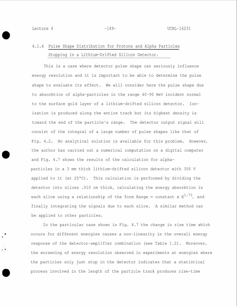
Lecture 4 -149- UCRL-16231
_
4.1.4 Pulse Shape Distribution for Protons and Alpha Particles
Stopping in a Lithium-Drifted Silicon Detector.
This is a case where detector pulse shape can seriously influence
energy resolution and it is important to be able to determine the pulse
shape to evaluate its effect. We will consider here the pulse shape due
to absorbtion of alpha-particles in the range 40-90 MeV incident normal
to the surface gold layer of a lithium-drifted silicon detector. Ion-
ization is produced along the entire track but its highest density is
toward the end of the particle's range. The detector output signal will
consist of the integral of a large number of pulse shapes like that of
Fig. 4.2. No analytical solution is available for this problem. However,
the author has carried out a numerical computation on a digital computer
and Fig. 4.7 shows the results of the calculation for alpha-
particles in a 3 mm thick lithium-drifted silicon detector with 350 V
applied to it (at 25°C). This calculation is performed by dividing the
detector into slices .010 cm thick, calculating the energy absorbtion in
each slice using a relationship of the form Range = constant x E1.73, and
finally integrating the signals due to each slice. A similar method can
be applied to other particles.
In the particular case shown in Fig. 4.7 the change in rise time which
occurs for different energies causes a non-linearity in the overall energy
response of the detector-amplifier combination (see Table 1.2). Moreover,
the worsening of energy resolution observed in experiments at energies where
the particles only just stop in the detector indicates that a statistical
process involved in the length of the particle track produces rise-time

Lecture 4 -150- UCRL-16231
variations which thereby cause a spread in pulse height ac the output of
the amplifier system.
4.2 RADIATION DAMAGE IN DETCTORS
Except in the case of some minor applications of detectors as radia-
tion dosimeters the only useful interactions between radiation and the
detector material are those producing hole-electron pairs in the material.
In this case the normal equilibrium of the material is restored in a very
short time and we use only the transient effect for measurements. However,
radiation in its many forms can interact with atoms in the lattice structure
and displace them from their lattice sites. Each such interaction produces
at least one vacancy and an interstitial atom in the lattice. This
vacancy-interstitial pair is known as a Frenkel pair or Frenkel defect.
In general, the atom ejected from its lattice site carries enough energy
to displace further atoms and more than one Frenkel pair is produced by
an interaction. The quantity of defects produced by a single interaction
and the probability of occurrence of a damaging interaction depends upon
the type and energy of the radiation. Dearnaley treats this problem in
some detail in his book18 and we will use his results in this discussion.
4.2.1 Damage Mechanism
The discussion which follows will deal with collisions between an
incoming particle and the semiconductor atoms. Gamma-rays interact in the
material to produce electrons with energies ranging up to the gamma-ray
energy and, therefore, the damage caused is similar to that of fast electrons.
Different types of particles react (with the atoms which constitute the
lattice) in different ways and this causes the amount and character of the
damage to differ considerably. Fast neutrons have very low probability of

Lecture 4 -151- UCRL-16231
producing direct hits with silicon* atoms but the average energy acquired
by the silicon atoms from the collisions is quite high. The resulting
energetic silicon atom produces many secondary defects and the overall
damage to the material is characterized by small highly damaged regions
separated by considerable amounts of undamaged material. In contrast to
this, heavy charged particles interact with silicon atoms by Rutherford
scattering (mutual electrical repulsion) so there are large numbers of
low energy exchanges and very few silicon atoms acquire high enough
energies to produce substantial numbers of secondary defects. Damage by
fast electrons is influenced largely by the fact that a silicon atom can
acquire little energy when an electron collides with it. Therefore damage
is limited almost entirely to the few silicon atoms which acquire suffi-
cient energy to be displaced from the lattice. For low electron energies
(< 250 keV in Si; < 600 keV in Ge) no collision can give sufficient energy
to a lattice atom to displace it. Measurements of the energy required to
displace a silicon atom indicate that 25 to 30 eV is necessary.
The case of slow neutron damage is a little different from those
discussed above. Here the capture of a neutron by Si30 (4% of silicon)
produces P31 and a β-particle whose energy ranges up to 1.5 MeV. Damage
of the Frenkel defect type is produced by the electrons as in the previous
paragraph. However, the phosphorous atoms now act as donors in the lattice
and the bulk resistivity changes. This can be considered to be damage or a
desirable result depending upon its effect on detector performance.**
Fortunately the cross-section for this process is small.
We will deal only with silicon in this discussion. Radiation damage ingermanium detectors used only for gamma-rays appears likely to be small.However, germanium detectors will be very susceptible to damage if used in asignificant flux of neutrons. The effects of the damage may not be evident,however, as long as the detector is maintained at a low temperature wherediffusion of lithium and vacancies is negligible.
**The production of P31 by slow neutron bombardment has been used as a methodof compensating p-type material to produce high resistivity silicon.20

Lecture 4 -152- UCRL-16231
A case which defies analysis is that of fission fragment damage.
The intense damage spike produced by the entry of highly charged heavy
particles and deposition in the lattice of radioactive nuclei is too
complicated a process to permit detailed understanding. However, in p-n
junction detectors, it is known that the damage tends to produce more
intrinsic material than was present before irradiation. This presumably
results from the production of donors and acceptors near the middle of
the band-gap of the material.
From these general considerations we conclude that the most important
types of damage to the nuclear spectrocopist, not concerned with heavy ion
or fission fragment research, are likely to be those due to fairly heavy
charged particles (such as protons or alpha particles) and to fast neutrons.
The cross section for fast neutron collisions is about 3 x 10-22 cm2
(corresponding to a mean free path of about 0.5 cm) and the energy distri-
bution of Si recoils is flat up to Emax where Emax is given by:
Emax = 0.133 En (4.15)
The average energy of the recoils is therefore half this value. The energy
of the silicon recoil atom is partly expended in producing ionization and
partly in producing secondary defects. As long as the silicon nucleus is
moving at high velocity it will be stripped of some of its atomic electrons
and therefore behave as a charged particle. As it slows down it will become
uncharged by capturing electrons. The threshold energy of an uncharged
silicon atom to produce ionization is 7 keV and therefore the minimum number
of defects per neutron collision (assuming ERECOIL > 7 keV) is 7000/Ed
where Ed is the energy required to displace a silicon atom.* This means
*Very little of the silicon atoms energy is likely to be lost to vibrationalmodes of the lattice as the wavelength equivalent of the silicon atom ismuch smaller than the lattice dimensions.

Lecture 4 -153- UCRL-16231
that each neutron collision produces a minimum of about 300 Frenkel pairs.
Depending upon the fraction of the primary silicon atom's recoil energy
used up in ionizing collisions before it slows down to the 7 keV level the
Emaxnumber of Frenkel pairs produced can range from 300 to about _ . If2 Ed
Emax = 1 MeV this upper limit is well over 1000 defects. It is likely
that most of the energy above 7 keV will be lost by ionizing collisions
and, for the moment, we will assume that 500 defects are produced per
fast neutron collision. 1010 neutrons/cm2 will then produce about 2 x 10⁹
primary recoils in a 0.1 cm thick (1 cm2) slab of silicon and 1012 total
Frenkel defects will be produced in the material as a result of this
bombardment.
In the case of charged particles, such as alpha-particles, the mean
energy acquired by the primary silicon recoils is low but the number of
primary recoils is large. Dearnaley has analyzed this situation and Fig. 4.3
shows his results for alpha-particles and protons. Integration of the curve
to determine the total number of defects produced by a 40 MeV alpha-particle
shows that it leaves about 400 defects along its track. This means that
1010 such alpha-particles will leave about 4 x 10¹² defects in a 0.1 cm
thick piece of silicon. This is about the same number as was calculated for
the fast neutron case but the defects have a different spatial distribution
in the material.
4.2.2 Consequences of Damage in p-n Junction Detectors
A confusing mass of literature exists on the results of radiation damage
to detectors. Most of the experimental data has been obtained under poorly
controlled conditions in which the measurement of damage was a secondary
objective in a nuclear experiment. Moreover the consequences of irradiation

Lecture 4 -154- UCRL-16231
depend on the type of detector and they may depend upon details of the
manufacturing process. To provide a logical interpretation of the results
some restrictions must be placed upon the scope of the following discussion.
In particular we will not discuss surface barrier detectors as the lack of
knowledge of the nature of the barrier makes it difficult to assess the
likely effect of radiation in the barrier itself. There is evidence that
the barrier is damaged by quite small doses of fission fragments ( ~ 107/cm2).
We will further restrict the discussion by eliminating consideration of any
deleterious effects produced by radiation in the surface layer at the edge
of the junction. There is evidence that surface properties can be affected
in certain radiation environments but the effects are complex and are quite
unimportant in the case of detectors used for spectroscopy.
These restrictions limit us to considering the coasequeaces of bulk
damage of the Frenkel defect type in silicon p-n junction and lithium drifted
silicon detectors. It is necessary to realize at the outset that the probable
consequences of damage to a detector are directly related to the ratio of the
number of active acceptor (or donor) atoms in the bulk to the number of
defects produced by the radiation. If few defects are produced compared with
the acceptor concentration,the effect of the damage on the detector properties
is likely to be small. A consequence of this is that p-n junction detectors -
particularly those made with low resistivity bulk material - are much less
prone to damage than lithium-drifted detectors. One might argue that this
is, in fact, a consequence of the thickness of the detector which is,
of course, related to the resistivity.

Lecture 4 -155- UCRL-16231
From Fig. 1.3 we see that the acceptor concentration in the bulk of
a detector made from 1000 ohm cm p-type silicon is about 2 x 10¹³ atoms/cm3.
We would therefore be surprised if a defect level close to this could not
be tolerated. According to Dearnaley's calculations this will correspond
to the damage produced by about 1011 alpha-particles (40 MeV), 1011 fast
neutrons, 5 x 10¹¹ protons (10 MeV) or 1014 fast electrons. Here we are
assuming that each defect finally behaves as an acceptor or donor. In fact,
the effects of damage become evident at just about these doses. However,
the details of the damage process and its precise effect in detector
characteristics are not easy to explain. In one group of detectors21 made
from p-type bulk material the effect of electron irradiation was to increase
the bulk resistivity but the effect of proton irradiation was the reverse.
In the first case, the damage did not anneal out over a long period of time
but it did so to a big extent in the second case. Any explanation for these
results must postulate the formation of different sets of levels due to the
defects or due to their migration through the lattice. Pairing of vacancies
and oxygen atoms has been postulated as one factor in this process. Pre-
sumably the striking difference between the effects of electrons and protons
must be associated with the different densities of defects in the "spikes"
produced by the two types of particles. One is tempted to explain the
recovery effect in the proton case by a partial re-association of vacancies
and interstitials in the rather dense damage track. If this is so, a similar
recovery might be expected after alpha-particle or fast neutron damage. To
my knowledge, detailed measurements on this have not been reported.
The use of p-n junction detectors in fission physics research has been
one of the most important areas of application of detectors for several years.
It has therefore been important to consider ways to reduce the sensitivity of

Lecture 4 -156- UCRL-16231
these detectors to fission fragment damage. P-N junction detectors made
on high resistivity p-type material (e.g., 2000 ohm cm) show severe damage
effects after doses of 107 to 108 fragments/cm2. As we might expect,
reduction of the bulk resistivity to 400 ohm cm has increased the useful
range into the 108 to 109 fragments/cm2 range. Furthermore, Gibson22 has
reported excellent radiation damage behaviour in thin punched-through
detectors operated at voltages much larger than those required to deplete
the thickness of the wafer. This might be anticipated since the detector
would be expected to operate reasonably well until the donor* (or acceptor)
density introduced by the damage process was high enough to prevent the
punch-through condition.
Apart from the effect of damage on the bulk resistivity of the detector
material (which causes electric field changes), the levels introduced in
the forbidden gap provide recombination and generation centers. Consequently
the detector leakage current tends to increase and significant amounts of
charge may disappear during the charge collection process. Since these
effects may not be uniform in the whole sensitive volume of the detector,
worsening of energy resolution and the appearance of multiple peaks in the
amplitude spectrum are common signs of substantial radiation damage.
4.2.3 Consequences of Damage in Lithium-Drifted Silicon Detectors.
From the considerations outlined in the previous section it will be
obvious that these detectors are more sensitive to damage than the p-n
junction detectors. In our experience the worst effect of the damage is
to prevent total depletion of the detector thickness by the applied voltage.
There is evidence that fission fragment damage at least in p-type materialtends to make the material change in an n-type direction.

Lecture 4 -157- UCRL-16231
We will consider a 3 mm thick silicon detector with 300 V applied to it.
We can easily show that this will only just be depleted if 2 x 10¹⁰
acceptors/cm3 are introduced uniformly through the material. In 3 mm
thickness this means that about 1010 acceptors/cm2 are permissable. From
section 4.3.1, we can see that 1010 neutrons/cm2 produce about 3 x 10¹²
defects in 3 mm of silicon. Alternatively 1010 40 MeV alphas/cm2 produce
about the same number of defects. We might therefore expect signs of
damage* to occur at neutron or alpha doses of about 108/cm2. Results in
agreement with this conclusion have been reported by Mann and Yntema23.
Our own experimental observations on damage in lithium-drifted silicon
detetors induced during nuclear reaction experiments in the bombarding
particle energy range from 20 to 120 MeV are of’ interest in throwing some
light on the damage process. In summary these results are as follows:
(a) For practical purposes, damage in such scattering experiments
is almost entirely due to fast neutrons. These neutrons originate
at the target, collimating slits, and in the carbon absorber of
the Faraday-cup. Clear proof that damage is due to neutrons is
afforded by the observation that damage is not confined to the
region of the collimating slit image in the detector.
(b) The dominant consequence of the damage is the appearance of a
dead layer at the entry window of the detector. Increasing the
applied voltage can correct this up to the limit at which edge
breakdown causes substantial noise.
*It seems likely, and is experimentally observed, that the failure to depletethe material, with consequent appearance of a dead layer at the entry faceof the detector, is the most impor tant consequence of damage. Leakagecurrent and charge loss during collection are negligible.

Lecture 4 -158-
(c) After irradiation, the effects of the damage increase by a large
factor over a period of several weeks. We deduce from this that
the vacancies/interstitial pairs have very little direct effect
on the electrical behavior of the detector. However, migration
of the vacancies and lithium atoms may cause lithium precipitation
at the vacancies in due course. Thus, the donors are slowly
removed and the material becomes uncompensated. A consequence
of this is that detectors show no signs of damage during experi-
ments until they have received neutron doses much larger than
the 108/cm3 mentioned earlier.
(d) No increase in leakage due to either surface or bulk effects is
noted at the radiation levels at which the previously mentioned
effects occur.
(e) No shift of peaks in spectra is observed, nor does the energy
resolution change until the dead layer appears.
(f) In fast coincidence experiments a change in timing is the first
apparent effect of radiation damage. In a sensitive experiment
this can be observed for a total dose an order of magnitude
smaller than that at which any dead layer is seen. The change in
timing results from electric field lines terminating on radiation
produced acceptors thereby reducing the electric field in the region
toward the back of the detector.
While some workers have reported cases where the characteristics have
been recovered by redrifting the lithium, our results, if correctly inter-
preted, offer little hope of any substantial improvement in the radiation
sensitivity of lithium-driited detectors. Almost perfect material is required
for thick detectors and an unfortunate consequence of radiation damage is that

Lecture 4 -159- UCRL-16231
we no longer have adequate material. Repurification of the mateial and
recrystallization may well be the only solution to damage in this case.
ACKNOWLEDGEMENTS
Many people have contributed ideas and effort to these notes. In
particular, I should like to thank W. Hansen, R. Lothrop, M. Roach,
B. Jarrett, D. Landis, R. Pehl, and S. Antman for spending valuable
time discussing various aspects of the lectures. My thanks are also
due to several experimenters in the Nuclear Chemistry Department of the
Lawrence Radiation Laboratory for their stimulation and constant interest
in developing and using detectors. Without their active support little
of this work would have been possible. Finally thanks are due to
Leo Schifferle and Mary Thibideau for their constant help in preparing
the script and figures.
This work was carried out as part of the program of the Nuclear
Chemistry Instrumentation Group of the Lawrence Radiation Laboratory
supported by A.E.C. contract No. W-7405-eng-48.
Lecture 4 -160- UCRL-16231
LECTURE 4. FIGURE CAPTIONS
Fig. 4.1 Collection of Hole-electron Pair in a p-i-n Detector
Fig. 4.2 Signal Output Due to a Single Electron Hole Pair in a p-i-n
Fig. 4.3 Collection of Hole-Electron Pair in a P-N-Junction
Fig. 4.4 Signal Output due to a Single Electron-Hole Pair in a P-N
Fig. 4.5 Expected Range of Pulse Shapes from p-i-n Germanium Detector at 77°K.
Fig. 4.6 Distribution in Triggering Delays of a Discriminator set to β-Peak
Pulse Amplitude from a Germanium Detector.
Fig. 4.7 Detector Pulse Shape for Alphas(Silicon Detector W = 3 mm,)
V = 350 V,
T = 25°C.
Fig. 4.8 Frenkel Defect Production by Alphas and Protons (Silicon)
(No Velocity Saturation Case)
Detector.
(No Velocity Saturation Case)
Junction Detector.
(Assuming V > 1000 Volts/cm)
(After Dearnaley)


-169- UCRL-16231
1. V. Fano, Phys. Rev. 70, 44 (1946).
2. V. Fano, Phys. Rev. 72, 26 (1947).
3. J. B. Birks, Theory and Practice of Scintillation Counting (Pergamon,
MacMillan, Co., New York, 1964) p. 662.
4. P. Iredale, Nuclear Inst. & Methods 11, 336 (1961).
5. P. Thieburger, et al., Proc. of Symposium on Nuclear Instruments,
Harwell, Sept., 1961 (Academic Press) p. 54.
6. W. Shockley, Proc. IRE 46, 973 (1958).
7. T. M. Buck, Semiconductor Nuclear Particle Detectors, N.R.C. Pub. #871,
p. 111 (1961).
8. F. S. Goulding, W. L. Hansen, N.R.C. Pub. #871, p. 202 (1961).
9. W. L. Hansen, F. S, Goulding, Nuclear Instr. & Methods 29, 345 (1964).
10. R. Deshpande, Solid State Electronics 8, 313 (1965).
11. H. Reiss, C. S. Fuller & F, J. Morin, Bell System Tech, Jour. XXXV,
535 (1956).
12. E. M. Pell, N.R.C. Pub. #871, p. 136 (1961).
13. W. L. Hansen, B. Jarrett, Nuclear Instr. & Methods 31, 301 (1964).
14. F. S. Goulding, W. L. Hansen, IEEE Trans. on Nucl. Sci. NS-11, 286 (1964).
15. A. J. Tavendale, IEEE Trans. on Nucl. Sci, NS-11, 191 (1964).
16. A. C. Prior, J. Chem. Phys, Solids 12, 175 (1960).
17. T. K. Alexander, et al., Phys. Rev. Letters 13, 86 (1964).
18. G. Dearnaley, D. C. Northrop, Semiconductor Counters for Nuclear
Radiations (John Wiley & Sons, Inc., New York, 1963).
19. (Not Used)

-170- UCRL-16231
20. J. Messier, et al., IEEE Trans. on Nucl. Sci. NS-11, 276 (1964).
21. R. E. Scott, IEEE Trans. on Nucl. Sci. NS-11, 206 (1964).
22. W. M. Gibson, Private Communication.
23. H. M. Mann & J. L. Yntema, IEEE Trans. on Nucl. Sci. NS-11, 201 (1964).
24. W. Van Hoosbroeck, Private Communication.
25. A. Van der Ziel, Proc. IRE 50, 1808 (1962).
26. A. Van der Ziel, Proc. IRE 51, 461 (1963).
27. O. Meyer, Nuclear Instr. & Methods 33, 164 (1965).
28. T. W. Nybakken, V. Vali, Nuclear Instr. & Methods 32, 121 (1965).

![AEC Tunnel Lighting AEC TUNNEL LIGHTING - …old.annell.se/AnnellFiles/Brochure_Tunnel_ENG_low_Del1[2].pdf · AEC Tunnel Lighting AEC TUNNEL LIGHTING | 3 NERO e GRIGIO per marchi](https://img.dokumen.tips/doc/110x75/5b733ee97f8b9a95348de2ee/aec-tunnel-lighting-aec-tunnel-lighting-old-2pdf-aec-tunnel-lighting-aec.jpg)