Embed Size (px)
Citation preview
- 1 -
TRXˍ024ˍ006 24-GHz Highly Integrated IQ Transceiver
Data Sheet Status: Date: Author: Filename:
final 2017-10-26 Silicon Radar GmbH DatasheetˍTRXˍ024ˍ006ˍV1.7
Version: Product number: Package: Marking: Page:
1.7 TRXˍ024ˍ006 QFN20, 3 × 3 mm² TRX006 YYWW
1 of 18
|Silicon Radar GmbH |Im Technologiepark 1
|15236 Frankfurt (Oder) |Germany
|fon +49.335.557 17 60 |fax +49.335.557 10 50
|http://www.siliconradar.com
24-GHz IQ Transceiver MMIC TRX_024_006
Data Sheet Version 1.7 2017-10-26
- 2 -
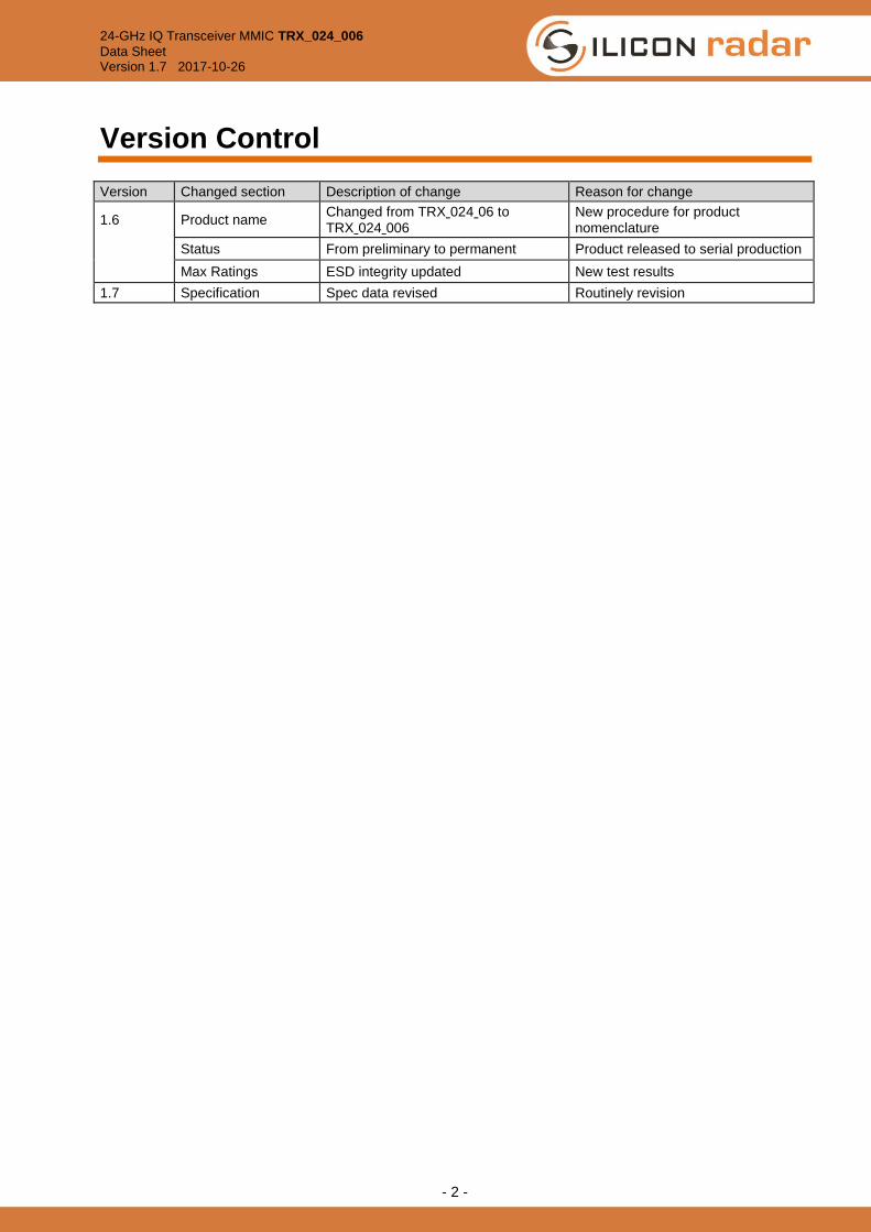
Version Control
Version Changed section Description of change Reason for change
1.6 Product name Changed from TRXˍ024ˍ06 to TRXˍ024ˍ006
New procedure for product nomenclature
Status From preliminary to permanent Product released to serial production
Max Ratings ESD integrity updated New test results
1.7 Specification Spec data revised Routinely revision
24-GHz IQ Transceiver MMIC TRXˍ024ˍ006
Data Sheet Version 1.7 2017-10-26
- 3 -
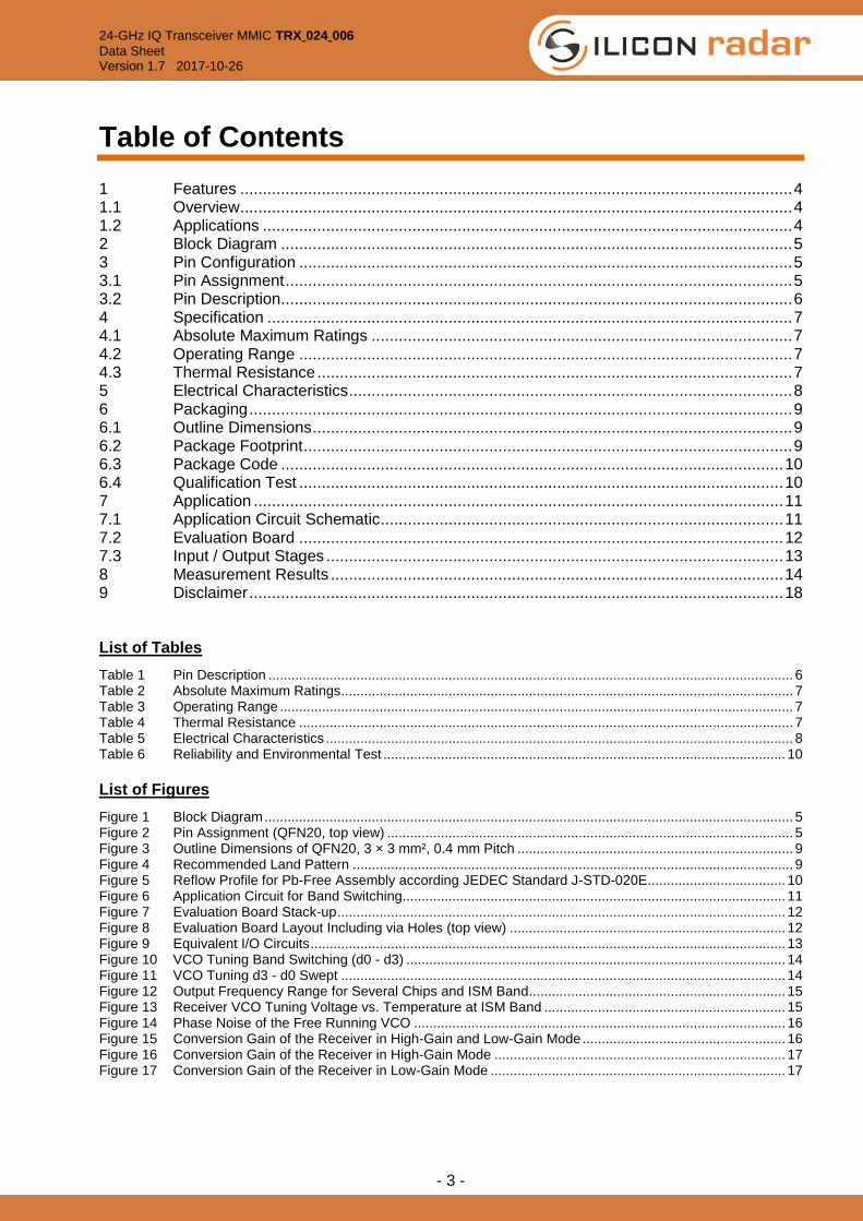
Table of Contents 1 Features .......................................................................................................................... 4 1.1 Overview .......................................................................................................................... 4 1.2 Applications ..................................................................................................................... 4 2 Block Diagram ................................................................................................................. 5 3 Pin Configuration ............................................................................................................. 5 3.1 Pin Assignment ................................................................................................................ 5 3.2 Pin Description ................................................................................................................. 6 4 Specification .................................................................................................................... 7 4.1 Absolute Maximum Ratings ............................................................................................. 7 4.2 Operating Range ............................................................................................................. 7 4.3 Thermal Resistance ......................................................................................................... 7 5 Electrical Characteristics .................................................................................................. 8 6 Packaging ........................................................................................................................ 9 6.1 Outline Dimensions .......................................................................................................... 9 6.2 Package Footprint ............................................................................................................ 9 6.3 Package Code ............................................................................................................... 10 6.4 Qualification Test ........................................................................................................... 10 7 Application ..................................................................................................................... 11 7.1 Application Circuit Schematic ......................................................................................... 11 7.2 Evaluation Board ........................................................................................................... 12 7.3 Input / Output Stages ..................................................................................................... 13 8 Measurement Results .................................................................................................... 14 9 Disclaimer ...................................................................................................................... 18 List of Tables
Table 1 Pin Description ......................................................................................................................................... 6 Table 2 Absolute Maximum Ratings...................................................................................................................... 7 Table 3 Operating Range ...................................................................................................................................... 7 Table 4 Thermal Resistance ................................................................................................................................. 7 Table 5 Electrical Characteristics .......................................................................................................................... 8 Table 6 Reliability and Environmental Test ......................................................................................................... 10 List of Figures
Figure 1 Block Diagram .......................................................................................................................................... 5 Figure 2 Pin Assignment (QFN20, top view) .......................................................................................................... 5 Figure 3 Outline Dimensions of QFN20, 3 × 3 mm², 0.4 mm Pitch ........................................................................ 9 Figure 4 Recommended Land Pattern ................................................................................................................... 9 Figure 5 Reflow Profile for Pb-Free Assembly according JEDEC Standard J-STD-020E.................................... 10 Figure 6 Application Circuit for Band Switching.................................................................................................... 11 Figure 7 Evaluation Board Stack-up ..................................................................................................................... 12 Figure 8 Evaluation Board Layout Including via Holes (top view) ........................................................................ 12 Figure 9 Equivalent I/O Circuits ............................................................................................................................ 13 Figure 10 VCO Tuning Band Switching (d0 - d3) ................................................................................................... 14 Figure 11 VCO Tuning d3 - d0 Swept .................................................................................................................... 14 Figure 12 Output Frequency Range for Several Chips and ISM Band................................................................... 15 Figure 13 Receiver VCO Tuning Voltage vs. Temperature at ISM Band ............................................................... 15 Figure 14 Phase Noise of the Free Running VCO ................................................................................................. 16 Figure 15 Conversion Gain of the Receiver in High-Gain and Low-Gain Mode ..................................................... 16 Figure 16 Conversion Gain of the Receiver in High-Gain Mode ............................................................................ 17 Figure 17 Conversion Gain of the Receiver in Low-Gain Mode ............................................................................. 17
24-GHz IQ Transceiver MMIC TRXˍ024ˍ006
Data Sheet Version 1.7 2017-10-26
- 4 -
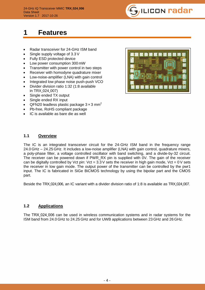
1 Features
Radar transceiver for 24-GHz ISM band
Single supply voltage of 3.3 V
Fully ESD protected device
Low power consumption 300 mW
Transmitter with power control in two steps
Receiver with homodyne quadrature mixer
Low-noise-amplifier (LNA) with gain control
Integrated low phase noise push-push VCO
Divider division ratio 1:32 (1:8 available in TRXˍ024ˍ007)
Single ended TX output
Single ended RX input
QFN20 leadless plastic package 3 × 3 mm2
Pb-free, RoHS compliant package
IC is available as bare die as well
1.1 Overview The IC is an integrated transceiver circuit for the 24-GHz ISM band in the frequency range 24.0 GHz – 24.25 GHz. It includes a low-noise amplifier (LNA) with gain control, quadrature mixers, a poly-phase filter, a voltage controlled oscillator with band switching, and a divide-by-32 circuit. The receiver can be powered down if PWR_RX pin is supplied with 0V. The gain of the receiver can be digitally controlled by Vct pin: Vct = 3.3 V sets the receiver in high gain mode, Vct = 0 V sets the receiver in low gain mode. The output power of the transmitter can be controlled by the pwr1 input. The IC is fabricated in SiGe BiCMOS technology by using the bipolar part and the CMOS part. Beside the TRXˍ024ˍ006, an IC variant with a divider division ratio of 1:8 is available as TRXˍ024ˍ007.
1.2 Applications The TRXˍ024ˍ006 can be used in wireless communication systems and in radar systems for the ISM band from 24.0 GHz to 24.25 GHz and for UWB applications between 23 GHz and 26 GHz.
24-GHz IQ Transceiver MMIC TRXˍ024ˍ006
Data Sheet Version 1.7 2017-10-26
- 5 -
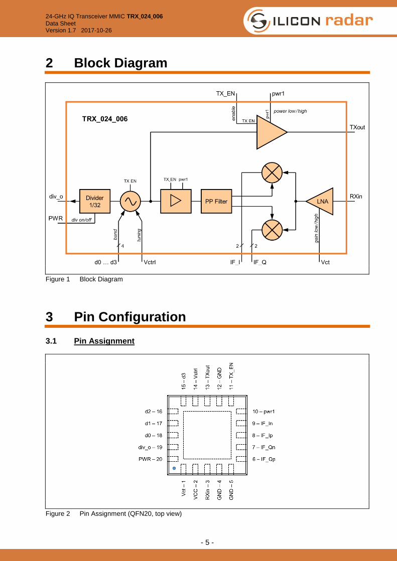
2 Block Diagram
Figure 1 Block Diagram
3 Pin Configuration
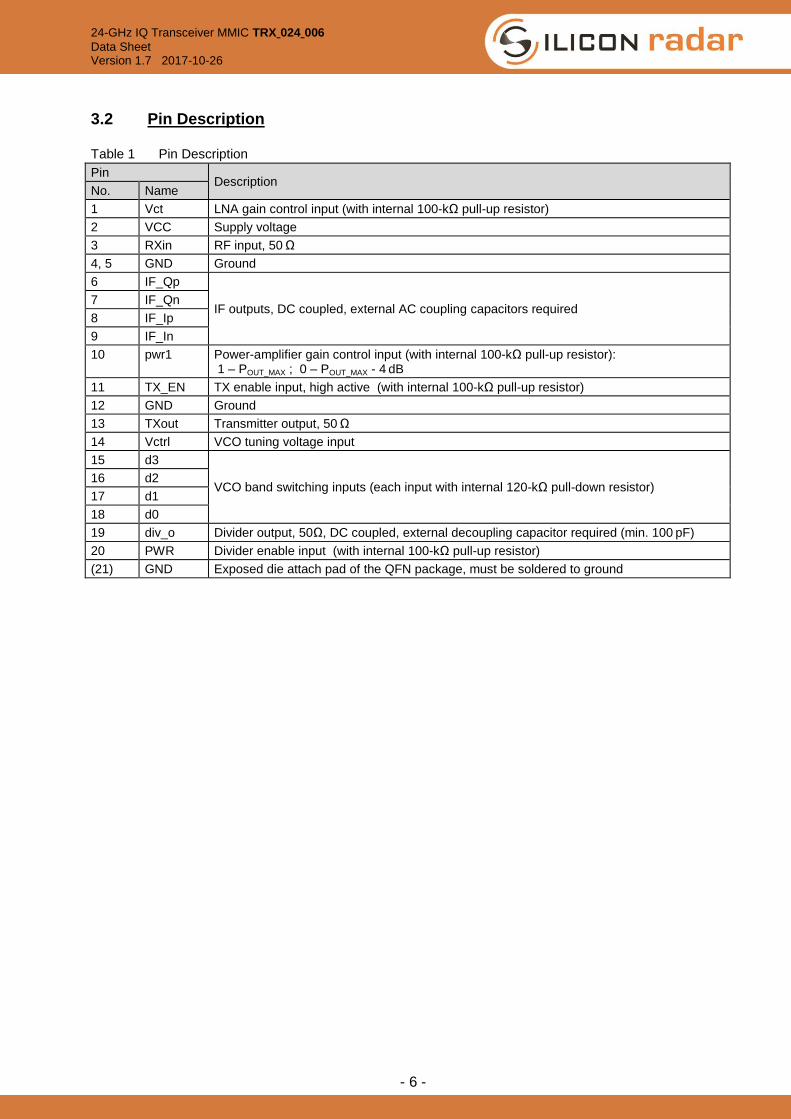
3.1 Pin Assignment
Figure 2 Pin Assignment (QFN20, top view)
24-GHz IQ Transceiver MMIC TRXˍ024ˍ006
Data Sheet Version 1.7 2017-10-26
- 6 -
3.2 Pin Description Table 1 Pin Description
Pin Description
No. Name
1 Vct LNA gain control input (with internal 100-kΩ pull-up resistor)
2 VCC Supply voltage
3 RXin RF input, 50 Ω
4, 5 GND Ground
6 IF_Qp
IF outputs, DC coupled, external AC coupling capacitors required 7 IF_Qn
8 IF_Ip
9 IF_In
10 pwr1 Power-amplifier gain control input (with internal 100-kΩ pull-up resistor): 1 – POUT_MAX ; 0 – POUT_MAX - 4 dB
11 TX_EN TX enable input, high active (with internal 100-kΩ pull-up resistor)
12 GND Ground
13 TXout Transmitter output, 50 Ω
14 Vctrl VCO tuning voltage input
15 d3
VCO band switching inputs (each input with internal 120-kΩ pull-down resistor) 16 d2
17 d1
18 d0
19 div_o Divider output, 50Ω, DC coupled, external decoupling capacitor required (min. 100 pF)
20 PWR Divider enable input (with internal 100-kΩ pull-up resistor)
(21) GND Exposed die attach pad of the QFN package, must be soldered to ground
24-GHz IQ Transceiver MMIC TRXˍ024ˍ006
Data Sheet Version 1.7 2017-10-26
- 7 -
4 Specification
4.1 Absolute Maximum Ratings Attempted operation outside the absolute maximum ratings of the part may cause permanent damage to the part. Actual performance of the IC is only guaranteed within the operational specifications, not at absolute maximum ratings. Table 2 Absolute Maximum Ratings
Parameter Symbol Min. Max. Unit Condition / Remark
Supply Voltage VCC 3.6 V to GND
DC voltage at RF pins VDCRF 0 2 mV IC provides low ohmic circuit to GND for TXout and RXin
Junction temperature TJ 150 °C
Storage temperature range TSTG -65 150 °C
DC voltage at control inputs VCTL -0.3 VCC + 0.3 V d0, d1, d2, d3, Vctrl
Input power into pin RFin PIN 0 dBm
ESD robustness 1)
VESD 500 V Class 1A 1)
1) According to ESDA/JEDEC Joint Standard for Electrostatic Discharge Sensitivity Testing, Human Body Model Component Level, ANSI/ESDA/JEDEC JS-001-2011
4.2 Operating Range Table 3 Operating Range
Parameter Symbol Min Max Unit Condition / Remark
Ambient temperature TA -40 85 °C
Supply voltage VCC 3.13 3.47 V (3.3V ± 5%)
DC voltage at control inputs VCTL 0 VCC V d0, d1, d2, d3, Vctrl
4.3 Thermal Resistance Table 4 Thermal Resistance
Parameter Symbol Min Typ Max. Unit Condition / Remark
Thermal resistance from junction to soldering point
RthJS 50 K/W
24-GHz IQ Transceiver MMIC TRXˍ024ˍ006
Data Sheet Version 1.7 2017-10-26
- 8 -
5 Electrical Characteristics TA = -40 °C ~ +85 °C unless otherwise noted. Typical values measured at TA = 25 °C and VCC = 3.3 V. Table 5 Electrical Characteristics
Parameter Symbol Min Typ Max Unit Condition / Remark
DC Parameters
Supply current consumption ICC 80 89 100 mA TX, divider enabled
Transmitter Section TX
Transmitter start frequency fTX 22.3 22.8 23.3 GHz
Transmitter stop frequency 25.9 26.4 26.9 GHz
Divider division ratio Ddiv_o 32 Note 1
Divider output frequency fdiv_o 700 840 MHz
Tuning voltage VCO Vctrl 0 3.3 V
Tuning slope VCO (Vctrl) ΔfTX/ΔVctrl 220 MHz/V Only Vctrl swept
Number of adjustable frequency bands
1)
16 d0 - d3: VCO band switching, Note 1
Pushing VCO ΔfTX/ΔVCC 135 MHz/V f = 24.15 GHz
Phase noise PN -102 -105 dBc/Hz at 1 MHz offset
Output impedance ZTXout 50
Transmitter output power PTX 2.5 4 6 dBm
Adjustable range output power (pwr1 pin)
PTX_ADJ 0 4 dBm Power amplifier gain control 1 – POUT_MAX 0 – POUT_MAX - 4 dBm
Divider output power 2)
Pdiv_o -9 -8.5 -8 dBm Note 2
Spurious power PSp- -40 dBm fTX - fdiv
PSp+ -43 dBm fTX + fdiv
Harmonics power PHa12 -46 dBm 12 GHz
PHa48 -40 dBm 48 GHz
Receiver Section TX
Receiver frequency fRX 22.3 26.9 GHz
Receiver input impedance ZRXIN 50
Number of adjustable gain modes
2 Adjustable LNA gain control
Gain high gain mode 18 dB Vct = 3.3 V
Gain low gain mode 11 dB Vct = 0
IF frequency range fIF 0 200 MHz
IF output impedance ZOUT 470 Differential
IQ amplitude imbalance 1.0 dB
IQ phase balance 10 deg
Noise figure (DSB) high gain mode
4 dB Simulated (double side band at fIF = 1 MHz)
Noise figure (DSB) low gain mode
6 dB Simulated
Input compression point 1dB ICP -20 -13 dBm
1) See also chapter “Measurement Results”, figure 10 and 11.
2) Divider output are loaded with 50, DC coupled, external decoupling capacitor ≥ 100 pF required.
24-GHz IQ Transceiver MMIC TRXˍ024ˍ006
Data Sheet Version 1.7 2017-10-26
- 9 -
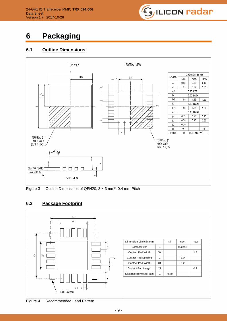
6 Packaging
6.1 Outline Dimensions
Figure 3 Outline Dimensions of QFN20, 3 × 3 mm², 0.4 mm Pitch
6.2 Package Footprint
Dimension Limits in mm min nom max
Contact Pitch E 0.4 BSC
Contact Pad Width W 1.8
Contact Pad Spacing C 3.0
Contact Pad Width X1 0.2
Contact Pad Length Y1 0.7
Distance Between Pads G 0.20
Figure 4 Recommended Land Pattern

24-GHz IQ Transceiver MMIC TRXˍ024ˍ006
Data Sheet Version 1.7 2017-10-26
- 10 -
Recommended Land Pattern
6.3 Package Code Top-Side Markings TRX006 YYWW
6.4 Qualification Test Table 6 Reliability and Environmental Test
Qualification Test JEDEC Standard Condition Pass / Fail
MSL3 J-STD-020E Reflow Simulation 3 times at 260°C pass
Tp ≤ Tc = tp ≤
TS.min = TS.max =
tS = TL = tL =
t25°C-to-Tp ≤
260 °C 30 s 150 °C 200 °C 60 s –120 s 217 °C 60 s – 150 s 480 s
Figure 5 Reflow Profile for Pb-Free Assembly according JEDEC Standard J-STD-020E
24-GHz IQ Transceiver MMIC TRXˍ024ˍ006
Data Sheet Version 1.7 2017-10-26
- 11 -
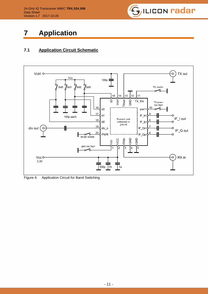
7 Application
7.1 Application Circuit Schematic
Figure 6 Application Circuit for Band Switching
24-GHz IQ Transceiver MMIC TRXˍ024ˍ006
Data Sheet Version 1.7 2017-10-26
- 12 -
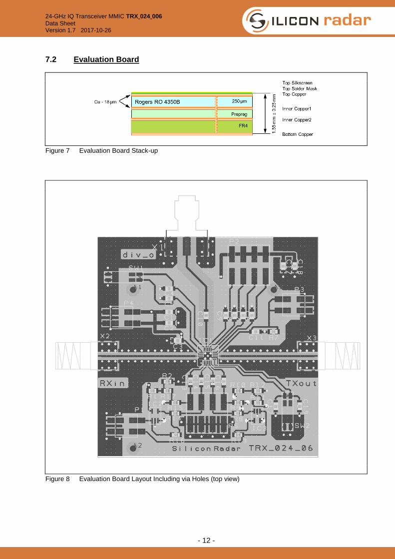
7.2 Evaluation Board
Figure 7 Evaluation Board Stack-up
Figure 8 Evaluation Board Layout Including via Holes (top view)
24-GHz IQ Transceiver MMIC TRXˍ024ˍ006
Data Sheet Version 1.7 2017-10-26
- 13 -
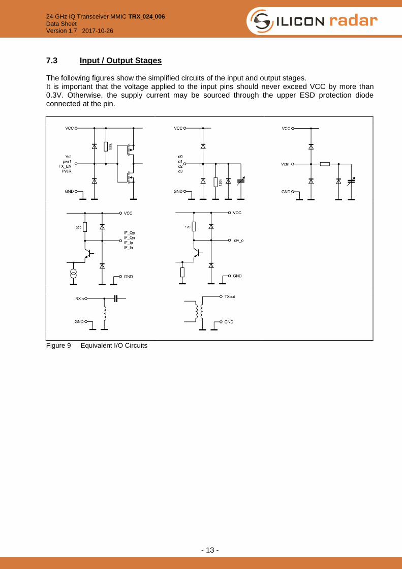
7.3 Input / Output Stages The following figures show the simplified circuits of the input and output stages. It is important that the voltage applied to the input pins should never exceed VCC by more than 0.3V. Otherwise, the supply current may be sourced through the upper ESD protection diode connected at the pin.
Figure 9 Equivalent I/O Circuits
24-GHz IQ Transceiver MMIC TRXˍ024ˍ006
Data Sheet Version 1.7 2017-10-26
- 14 -
8 Measurement Results
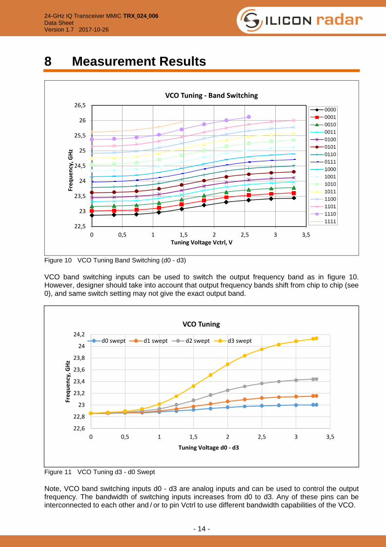
Figure 10 VCO Tuning Band Switching (d0 - d3)
VCO band switching inputs can be used to switch the output frequency band as in figure 10. However, designer should take into account that output frequency bands shift from chip to chip (see 0), and same switch setting may not give the exact output band.
Figure 11 VCO Tuning d3 - d0 Swept
Note, VCO band switching inputs d0 - d3 are analog inputs and can be used to control the output frequency. The bandwidth of switching inputs increases from d0 to d3. Any of these pins can be interconnected to each other and / or to pin Vctrl to use different bandwidth capabilities of the VCO.
22,5
23
23,5
24
24,5
25
25,5
26
26,5
0 0,5 1 1,5 2 2,5 3 3,5
Fre
qu
en
cy, G
Hz
Tuning Voltage Vctrl, V
VCO Tuning - Band Switching
0000
0001
0010
0011
0100
0101
0110
0111
1000
1001
1010
1011
1100
1101
1110
1111
22,6
22,8
23
23,2
23,4
23,6
23,8
24
24,2
0 0,5 1 1,5 2 2,5 3 3,5
Fre
qu
en
cy, G
Hz
Tuning Voltage d0 - d3
VCO Tuning
d0 swept d1 swept d2 swept d3 swept

24-GHz IQ Transceiver MMIC TRXˍ024ˍ006
Data Sheet Version 1.7 2017-10-26
- 15 -
Figure 12 Output Frequency Range for Several Chips and ISM Band
The input settings for the measurement shown in figure 8 are d3 = 0 (0 V), d2 = 1 (3.3 V). Inputs d0, d1, and Vctrl interconnected and swept together.
Figure 13 Receiver VCO Tuning Voltage vs. Temperature at ISM Band
The input settings for the measurement shown in figure 13 are d3 = 0 (0 V), d2 = 1 (3.3 V). Inputs d0, d1, and Vctrl interconnected and swept together.
24-GHz IQ Transceiver MMIC TRXˍ024ˍ006
Data Sheet Version 1.7 2017-10-26
- 16 -
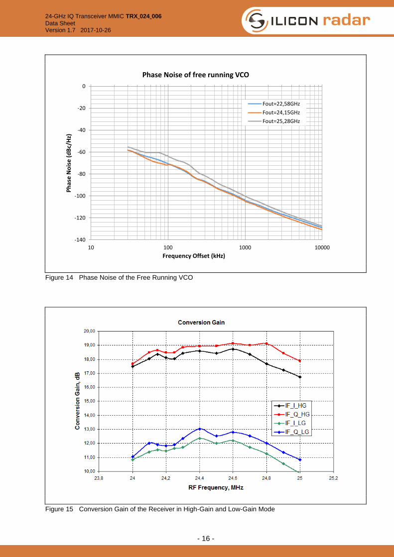
Figure 14 Phase Noise of the Free Running VCO
Figure 15 Conversion Gain of the Receiver in High-Gain and Low-Gain Mode
-140
-120
-100
-80
-60
-40
-20
0
10 100 1000 10000
Ph
ase
No
ise
(d
Bc/
Hz)
Frequency Offset (kHz)
Phase Noise of free running VCO
Fout=22,58GHz
Fout=24,15GHz
Fout=25,28GHz
24-GHz IQ Transceiver MMIC TRXˍ024ˍ006
Data Sheet Version 1.7 2017-10-26
- 17 -
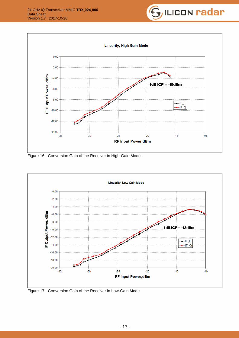
Figure 16 Conversion Gain of the Receiver in High-Gain Mode
Figure 17 Conversion Gain of the Receiver in Low-Gain Mode
24-GHz IQ Transceiver MMIC TRXˍ024ˍ006
Data Sheet Version 1.7 2017-10-26
- 18 -
9 Disclaimer Silicon Radar GmbH 2012. The information contained herein is subject to change at any time without notice. Silicon Radar GmbH assumes no responsibility or liability for any loss, damage or defect of a Product which is caused in whole or in part by
(i) use of any circuitry other than circuitry embodied in a Silicon Radar GmbH product, (ii) misuse or abuse including static discharge, neglect or accident, (iii) unauthorized modification or repairs which have been soldered or altered during assembly and are not capable of being
tested by Silicon Radar GmbH under its normal test conditions, or (iv) improper installation, storage, handling, warehousing or transportation, or (v) being subjected to unusual physical,
thermal, or electrical stress. Disclaimer: Silicon Radar GmbH makes no warranty of any kind, express or implied, with regard to this material, and specifically disclaims any and all express or implied warranties, either in fact or by operation of law, statutory or otherwise, including the implied warranties of merchantability and fitness for use or a particular purpose, and any implied warranty arising from course of dealing or usage of trade, as well as any common-law duties relating to accuracy or lack of negligence, with respect to this material, any Silicon Radar product and any product documentation. products sold by Silicon Radar are not suitable or intended to be used in a life support application or component, to operate nuclear facilities, or in other mission critical applications where human life may be involved or at stake. All sales are made conditioned upon compliance with the critical uses policy set forth below. CRITICAL USE EXCLUSION POLICY BUYER AGREES NOT TO USE SILICON RADAR GMBH'S PRODUCTS FOR ANY APPLICATION OR IN ANY COMPONENTS USED IN LIFE SUPPORT DEVICES OR TO OPERATE NUCLEAR FACILITIES OR FOR USE IN OTHER MISSION-CRITICAL APPLICATIONS OR COMPONENTS WHERE HUMAN LIFE OR PROPERTY MAY BE AT STAKE. Silicon Radar GmbH owns all rights, title and interest to the intellectual property related to Silicon Radar GmbH's products, including any software, firmware, copyright, patent, or trademark. The sale of Silicon Radar GmbH products does not convey or imply any license under patent or other rights. Silicon Radar GmbH retains the copyright and trademark rights in all documents, catalogs and plans supplied pursuant to or ancillary to the sale of products or services by Silicon Radar GmbH. Unless otherwise agreed to in writing by Silicon Radar GmbH, any reproduction, modification, translation, compilation, or representation of this material shall be strictly prohibited.