Embed Size (px)
Citation preview
Trembling electrons cause conductance fluctuation
∗Yu Iwasaki, Yoshiaki Hashimoto, Taketomo Nakamura, ShingoKatsumoto
Institute for Solid State Physics, University of Tokyo, 5-1-5 Kashiwanoha, Kashiwa, Chiba277-8581, Japan
E-mail: [email protected]
Abstract. The highly successful Dirac equation can predict peculiar effects such as Kleintunneling and the “Zitterbewegung” (German for trembling motion) of electrons. From thetime it was first identified by Erwin Schrodinger, Zitterbewegung (ZB) has been considereda key to understanding relativistic quantum mechanics. However, observing the original ZBof electrons is too difficult, and instead various emulations using entity models have beenproposed, producing several successes. Expectations are high regarding charge transportsin semiconductors and graphene; however, very few reports have appeared on them. Here,we report that ZB has a surprisingly large effect on charge transports when we play “flatpinball” with such trembling electrons in a semiconductor nanostructure. The stage here is anarrow strip of InAs two-dimensional electron gas with a strong Rashba spin-orbit coupling.Six quantum point contacts (QPCs) are attached to the strip as pinball pockets. The ZBappeared as a large reproducible conductance fluctuation versus in-plane magnetic fields in thetransport between two QPCs. Numerical simulations successfully reproduced our experimentalobservations, certifying that ZB causes a new type of conductance fluctuation.
In 1930, Erwin Schrodinger [1] found that a free particle described by the relativistic Diracequation undergoes oscillatory motion with the light velocity c. This phenomenon, calledZitterbewegung (meaning “trembling motion” and abbreviated as ZB), originates from thepure quantum nature of relativistic velocity, which does not commute, as an operator, withthe Dirac Hamiltonian. This means the velocity, despite long being a most familiar quantity tophysicists, is not a good quantum number for a free relativistic particle. Although interest in thisremarkable nature was stimulated among researchers, its estimated amplitude ~/m0c ∼ 386 fm,and the frequency 2m0c
2/~ ∼ 1.6×10²¹ rad./s for electrons, keep it very far out of experimentalreach [2]. Successful ZB emulations have been achieved in entity models, including those with asingle trapped ion [3] and ultra-cold atoms in Bose-Einstein condensates [4, 5]. However, clearobservation of ZB in more realistic emulations with electrons themselves in artificial vacuums,namely in solids [6–8], has been a major open task. In two-dimensional electron systemswith Rashba-type spin-orbit coupling (SOC) [9], ZB is predicted to appear as a meanderingof charge density [6] with relatively large amplitude of more than ten nanometers [8], whichis still barely observable by utilizing nanoscale techniques and superfine structures (although apossible observation was reported in a mesoscopic device [10]).
Here, we report observation of ZB as reproducible conductance fluctuation (CF) versusmagnetic fields in an InAs two-dimensional electron gas (2DEG) fabricated into an open billiardgeometry, which has quantum point contacts (QPCs) as emitters and billiard pockets. However,the experiment can be viewed as a pinball on a flat table (see Fig.1) rather than as a billiard,because the table has a considerable number of fixed scatterers (impurities). The “flat pinball
arX
iv:1
611.
0665
7v1
[co
nd-m
at.m
es-h
all]
21
Nov
201
6

with trembling electrons” model is also verified using a numerical simulation, which exhibitsmeandering of charge density and reproduces CF.
ResultsZB in Rashba modelLet us briefly view how ZB appears in the Rashba model described by the Hamiltonian
H =p2
2m∗ + (a+ b) · σ, a ≡ α
~
(py−px
), b ≡ g∗
2µB
(Bx
By
), σ ≡
(σxσy
), (1)
where p is the electron momentum, m∗ the effective mass, α the Rashba SOC parameter, g∗
the effective Lande g-factor, µB the Bohr magneton, B ≡ Bxx + Byy (with x, y as the unitcoordinate vectors) the in-plane magnetic flux density, and σx,y the Pauli matrices. As an initialcondition (t = 0), we consider an electron with a spin state of z-up in a Gaussian wavepacket
at an origin with central wave vector k = k0kx (vector along kx with size k0). After a timeevolution of t, the expectation value of the y-coordinate for finite |a+ b| is [11],
〈y(t)〉 =α
2
(a+ b)y[~ω(k0)]2
{1− cos[ω(k0)t]}, (2)
where~ω(k0) = |a+ b|, (3)
while the spin portion of the wavefunction is written as (cos[ω(k0)t], sin[ω(k0)t]). In the limitα→ 0, the amplitude of the ZB in Eq.(2) vanishes while it approaches k−1
0 for α→∞.Figure 2 (a) shows a schematic trace of the wavepacket oscillating along y according to Eq.(2)
with spin directions. As is easily understood, in a Rashba system, ZB appears as a meanderingelectron orbit with a spin precession around the vector sum of B and an effective magnetic fieldoriginating from SOC
Beff =2
g∗µBa =
2α
g∗µB
(k0
0
), (4)
which is perpendicular to the momentum.In the above formulas, the difficulties in the detection are apparent in that 1) the ZB
amplitude is the Fermi wavelength at most, and 2) to attain this amplitude the ZB frequency inEq.(3) should be very high above 1 THz. In the following, we consider solving these problemsin the introduction of the experimental setup.
xϕ
θ
yB
z
Figure 1. Pinball on a flat table. Electrons (green balls) are shot by QPCs (blue) into a2DEG (yellow) with scattering by impurities (red cylinders).
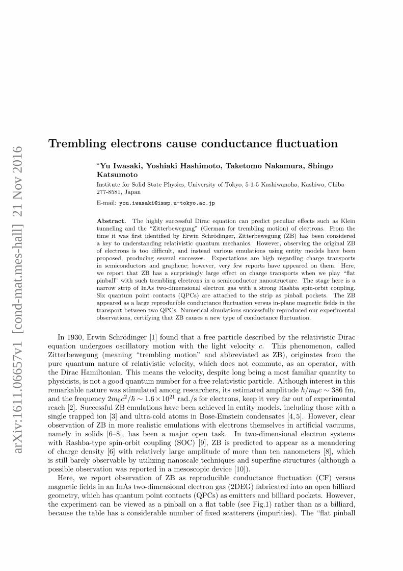
Experimental setupTo create a Rashba system, a 2DEG in a pseudomorphic InAs quantum well was grown withmolecular beam epitaxy. The layered structure has asymmetric (In,Ga)As/InAs interfaces inthe well region, whose structure is commonly adopted for strong Rashba SOI [12]. The electronmobility µ = 6.6×104 cm2/Vs and the sheet carrier concentration n = 1.1 × 10¹² /cm2 wereobtained from the longitudinal and Hall resistances. They produced the Fermi wavenumberkF= 2.6×10⁸ m−1, which corresponds to wavelength λF =2.4×10⁻⁸ m. The effects of quantumconfinement, wavefunction penetration into (In,Ga)As, and strain is renormalized into a shift inthe in-plane effective mass in InAs from bulk value 0.023m0 to 0.025m0 [13]. Then, the Fermivelocity vF = 1.2 × 10⁶ m/s and the Fermi energy EF = 106 meV, g∗ =8.6 [14] were obtained.The Rashba parameter α = 3.6 × 10⁻¹¹ eVm was obtained from the amplitude modulation ofthe Shubnikov-de Haas (SdH) conductance oscillation [15]. These parameters give the effectivemagnetic field strength (4) as 38 T, hence the ZB frequency 4.6 THz.
The high frequency problem can be solved by fixing the ZB in a steady state by usingspin-polarized electrons. This can be accomplished with a quantum point contact (QPC) on theconductance plateau of quantum conductance Gq ≡ 2e2/h, which was predicted theoretically [16]and confirmed experimentally [17]. Figure 2 (c) illustrates how the mechanism works to polarize
(b)(a)
(c)
A
k
E
B
C
(1, )
(1, )
(2, )(2, )
1 μm12
3
4 5 6
7
8
Bx
yφ
G1 G2 G4 G5 G6 G8
1.04 1.04 1.08 1.03 1.24 1.04
y (arb. unit)
t (ar
b. u
nit)
Figure 2. Experimental setup. (a) illustrates a ZB in the Rashba model. An electronwavepacket, with a spin parallel to the z-axis and an averaged momentum along x at timet = 0, oscillates along the y-axis in synchronization with the spin rotation in the z-x plane. (b)illustrates a scanning electron micrograph of the sample with the terminal numbers superposed.Pink false-colored areas act as gates isolated by trenches to define QPCs. Below the micrograph,the conductances of QPCs are listed in the unit of Gq (T = 55 mK). (c) illustrates dispersionsfor one-dimensional bands in a QPC with a Rashba SOI. The red and blue curves show up anddown spins, respectively. The extension of a crossing point reveals a small avoided crossing,which causes a spin rotation (and hence spin polarization) during an adiabatic transmissionthrough the QPC. A, C, and B indicate the positions of Fermi energy during the traversal atthe outlet, at the middle, and at a point between them, respectively [16].
spins of electrons passing through a QPC with Rashba SOI on the conductance plateau of Gq.On the top of the effective potential in the QPC, the Fermi energy places at the lowest branchin the discrete dispersion relations. When an electron passes through the QPC adiabatically,its energy shifts as A → B → C → B’ → A’. During the transition from C to B’, the avoidedcrossing between (0↓) and (1↑) flips up the electron spin. Owing to the “one-way spin rotation,”the spin polarization on plateau Gq reaches 0.7. Here, the spin separation of the dispersionbranch comes from the αpxσy/~ term, and the avoided crossing comes from −αpxσy/~ in (1).The Rashba SOI is thus necessary for the spin polarization.
Figure 2(b) shows a scanning electron micrograph from the sample, on which the numbersof the terminals are indicated. A right-handed spatial coordinate with a z-axis perpendicularto the 2DEG plane is taken as illustrated. The structure was fabricated with electron beamlithography and dry etching of trenches. Such trench-gate techniques are commonly used inInAs-based heterostructures [18], to which the Schottky gate technique is hardly applicable.The structure consists of a main conducting strip (terminal 3-7) with a width of 2 µm and sixQPCs opened on it. A problem here is that the gates (pink false-colored regions) are commonwith the neighboring ones and individual control of QPC conductance is difficult. Fortunately,after several cut-and-tries, we succeeded in tuning the QPC conductances at around 1.0Gq withall the gates grounded (except QPC-6), as shown in Fig.2(b). The fact that such coarse tuningwas successful indicates that the QPCs are on the 1.0Gq plateau, where the conductance is lesssensitive to the gate voltages than in other regions.
Then, in a conduction through any two of the QPCs, we emit spin-polarized electrons into themain strip region in one QPC and collect them through the other one. Owing to the electron-hole symmetry, this holds even for conduction paths with QPC-6, in which the polarization maybe insufficient. However, the effective opening of the QPCs is around 500 nm, which is still muchwider than the maximum amplitude of ZB. Here, we attempt to solve the problem by using thescatterers in the strip as amplifiers of the meandering motions. Because the width of the presentmean free path l0 ∼1 µm is about half that of the main strip, the emitted electrons shouldexperience a few scatterings before reaching a pocket. If we approximate such a scattering witha classical scattering for a hard cylindrical wall with radius R, the scattering angle γ for impactfactor bi is γ = 2 cos−1(bi/R). When bi oscillates against in-plane magnetic field B througha ZB with amplitude ∆bi, the oscillation is amplified to l0∆bi/R. The potential range R isroughly estimated to be an effective Bohr radius of 34 nm in InAs, which is even smaller thank−1
F . Hence, the amplified ZB can reach the order of l0 ∼ 1 µm, which can be resolved with thepresent QPCs.
The above rough classical sketch of scattering should be largely corrected in quantummechanics, in that the spread of wave packets weakens the amplification. As in the spin-polarization mechanism illustrated in Fig.2 (c), the wave packets emitted from a QPC shouldcover at least 2k−1
F . However, as shown experimentally in scanning gate microscopy [19], the wavepackets emitted from a QPC travel for surprisingly long distances without smooth spreading,owing to a kind of focusing effect. Therefore, we can expect that the above classical modelcan be half-quantitatively applicable. The experimental setup here can be viewed as a gameof pinball on a flat table with six pockets. The ball (wave packet) size may be larger than thepins (scattering centers), although minor wobbling in the orbits (the ZB) is amplified by thescattering.
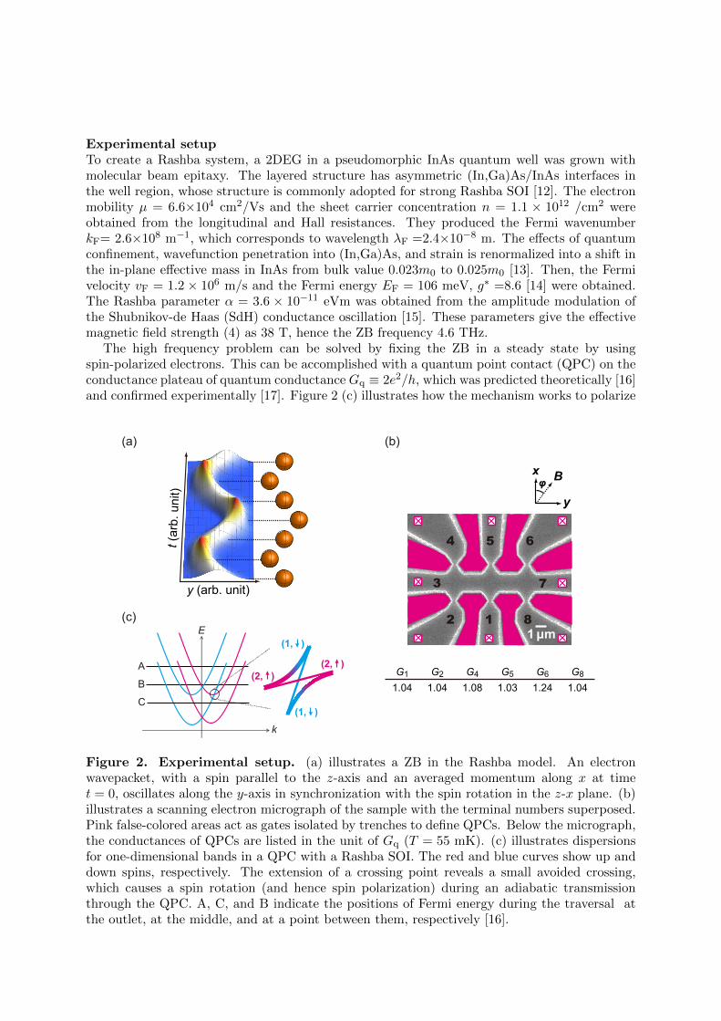
Conductance fluctuationsHenceforth, we use the notation Gi-j for the two-wire conductance between terminals i and j.Figure 3 (b) shows temperature variation of the two-wire conductance G1-5 as a function of thein-plane magnetic field along y-axis By. When the temperature was decreased, some aperiodicconductance oscillation versus By became visible and the amplitude increased. The oscillation
is reproducible, that is, almost the same pattern appears for two independent field sweepsat the same temperature, as demonstrated in Fig. 3 (a). Resemblances are also appreciablebetween the patterns for different temperatures. Such conductance fluctuations (CFs), that is,the aperiodic response to an external magnetic field, were observed for an arbitrary combinationof two electrodes for QPC connections.
The result indicates that ZB is modulated by an external magnetic field and appears as CFsin the pinball model. However, these remarkable features of CFs are also reminiscent of so-calleduniversal conductance fluctuation (UCF) [20]. We should thus check for the possibility of UCF.Because the applied field is in-plane, we can eliminate the quantum interference effect throughrandom paths tuned via the Aharonov-Bohm (AB) phase. However, there still remains thepossibility of interference in the spin portion of the wavefunction, which is modified by a spinprecession tuned via the in-plane magnetic field (spin-UCF) [21]; for the elimination, we needthe following two experiments.
The first is the rotation of the field direction from in-plane to perpendicular-to-plane (i.e.,rotating the elevation angle from 0 to π/2). The result is shown in Fig.3 (c). There is nosignificant variation in the amplitude and frequency distribution resulting from the patternchanges involving the angle. This is hardly conceivable for interference type CF, because ifthere is such a network of spatial interference and the perpendicular component of the field isincreased, the AB phase modulation participates in the interference modulation, which shouldbring some qualitative and systematic changes in the CF that stem from the geometric nature ofthe AB phase. The second is the magnetic response of G3-7, i.e., a transport without QPCs (andhence without spin polarization). Figures 3 (d, e) display the result, which exhibits a dramaticchange from Fig. 3 (c), in that in G3-7 almost no fluctuation is observable in the in-plane fieldand ordinary SdH oscillation appearing in the perpendicular field (although the SOI modulationis reduced, probably by loose confinement into the strip). This also indicates that the CFs arenot from an interference because if such an interference exists, it inevitably appears in G3-7, thepath of which goes through the strip.
The most plausible origin of the CFs is now the ZB modulation of scattering in the pinballsystem; thus, we further check the nature of CFs. The pinball model has two temperaturefactors; one is the spin polarization at QPCs and the other is the strength of the effective fieldBeff . The latter is related to Rashba splitting, which is approximately 6 K in the present case.The CF is visible at order-of-magnitude lower temperatures. Hence, the temperature dependenceobserved in Fig.3 (b) should come from spin polarization, which depends on the energy diagraminside the QPCs. Derivation of the explicit temperature dependence is difficult, although theorder estimation is reasonable because the effective EF is lower by an order of magnitude insidethe QPCs.
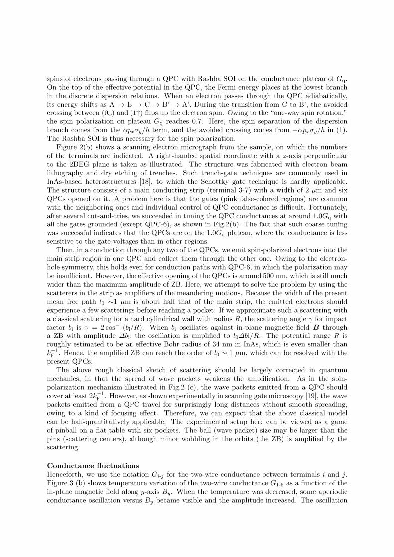
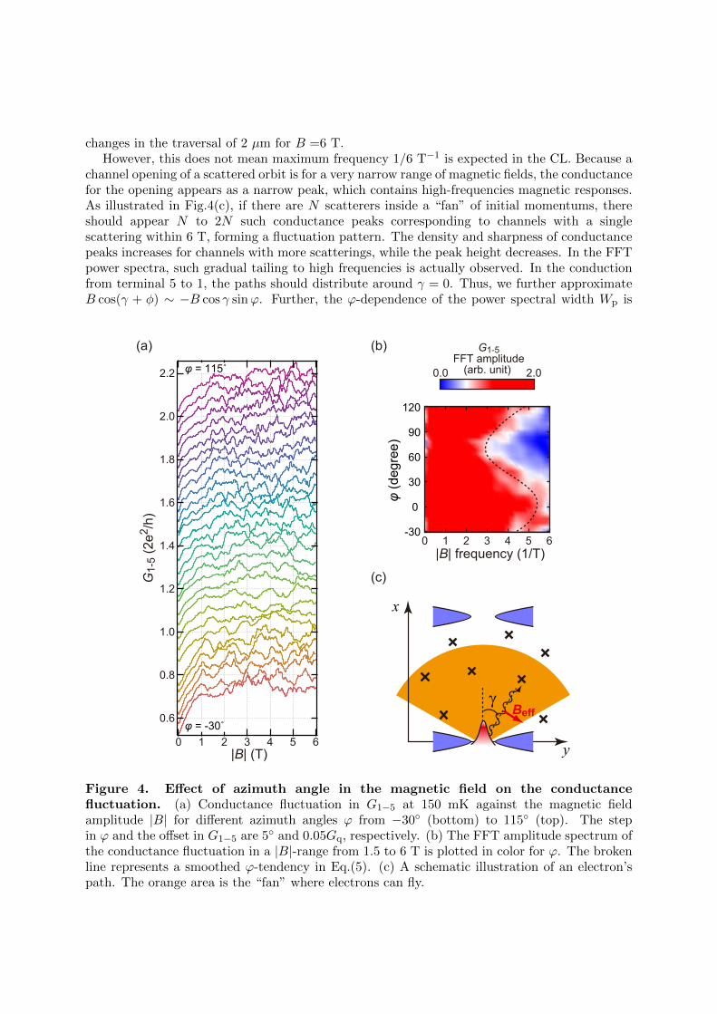
Azimuth angle dependenceFigure 4 (a) shows the variation of CF on the azimuth angle ϕ for an in-plane magnetic field.The fluctuation pattern changes with ϕ according to its resemblance to neighboring patterns.A frequency amplitude spectra obtained with a fast Fourier transform (FFT) is shown in Fig.4(b); it indicates some systematic angular dependence in the width of spectra.
Let us check the correspondence between the pinball game model and the experimental results.Because the spin polarization is along the y-axis directly near the emitter QPC [16], the electronswith momentum parallel to the x-axis do not tremble because Beff is perpendicular to themomentum from Eq.(1), which is parallel to the spins. Now we consider a path with an obliqueangle γ to the x-axis (Fig.4(c)). The length of Beff +B is approximated as Beff +B cos(γ + φ),where B is the external field strength and φ ≡ π/2 − ϕ for |Beff | � |B|. The “wavelength” ofZB is estimated as λZB ≡ π~2/αm∗ ≈ 270nm and the maximum modification of λZB with anexternal field for B =6 T and γ + φ = 0 is 34 nm. This means only a single cycle of meander

(a) (b)
(c)
(d)
(e)
4
5
6
7
8
9
G3-
7 (2
e2 /h)
Bz (T)6543210
6
|B| (T)
G1-
5 (2
e2 /h)
65432100.6
0.8
1.2
1.6
1.8
1.4
1.0
θ = 0˚
θ = 90˚
0.6
0.4
0.8
1.2
1.0
1.4
1.8
1.6
G1-
5 (2
e2 /h)
T = 4.2 KT = 4.2 K
T = 4.2 KT = 1.0 K
T = 4.2 KT = 0.5 K
T = 4.2 KT = 0.3 K
T = 4.2 KT = 0.15 K
By (T)6543210
G1-
5 (2
e2 /h)
By (T)543210
0.4
1.0
0.9
0.8
0.7
0.6
0.51
5
6.1
5.9
6.3
G3-
7 (2
e2 /h)
By (T)6543210
73
Figure 3. Reproducible conductance fluctuation against a magnetic field. (a) G1−5
is shown as a function of By for two individual magnetic sweeps with offset = 0.1Gq. The insetshows the terminal configuration. (b) G1−5 for different temperatures with offset = 0.2Gq. In(c), G1−5 at 70 mK is plotted versus the field amplitude |B|. The direction of the magneticfield (the zenith angle θ) is rotated from θ = 0 to 90◦ at azimuth angle ϕ =90◦. The steps inthe angle and conductance offsets are 10◦ and 0.2Gq, respectively. In (d) and (e), G3−7 (theconfiguration shown in the inset) at 70 mK is plotted as a function of By and Bz, respectively.
changes in the traversal of 2 µm for B =6 T.However, this does not mean maximum frequency 1/6 T−1 is expected in the CL. Because a
channel opening of a scattered orbit is for a very narrow range of magnetic fields, the conductancefor the opening appears as a narrow peak, which contains high-frequencies magnetic responses.As illustrated in Fig.4(c), if there are N scatterers inside a “fan” of initial momentums, thereshould appear N to 2N such conductance peaks corresponding to channels with a singlescattering within 6 T, forming a fluctuation pattern. The density and sharpness of conductancepeaks increases for channels with more scatterings, while the peak height decreases. In the FFTpower spectra, such gradual tailing to high frequencies is actually observed. In the conductionfrom terminal 5 to 1, the paths should distribute around γ = 0. Thus, we further approximateB cos(γ + φ) ∼ −B cos γ sinϕ. Further, the ϕ-dependence of the power spectral width Wp is
(a) (b)
(c)
0 1 32 4 5 6|B| frequency (1/T)
G1-5FFT amplitude
(arb. unit) 0.0 2.0
φ (d
egre
e)
-30
120
90
60
30
0
0.6
0.8
1.2
1.0
1.4
1.6
1.8
2.0
2.2
0 1 32 4 5 6|B| (T)
G1-
5 (2
e2 /h)
φ = 115˚
φ = -30˚
γBeff
x
y
Figure 4. Effect of azimuth angle in the magnetic field on the conductancefluctuation. (a) Conductance fluctuation in G1−5 at 150 mK against the magnetic fieldamplitude |B| for different azimuth angles ϕ from −30◦ (bottom) to 115◦ (top). The stepin ϕ and the offset in G1−5 are 5◦ and 0.05Gq, respectively. (b) The FFT amplitude spectrum ofthe conductance fluctuation in a |B|-range from 1.5 to 6 T is plotted in color for ϕ. The brokenline represents a smoothed ϕ-tendency in Eq.(5). (c) A schematic illustration of an electron’spath. The orange area is the “fan” where electrons can fly.
roughly written as
Wp(ϕ) ∝ l0λ2
ZB
∣∣∣∣∆λZB
∆B
∣∣∣∣ = l0πg∗µB
vF| sinϕ|, (5)
where l0 is the averaged ZB path length. Although the approximation is very coarse, Eq.(5)suggests that Wp takes a maximum around 90◦ and a minimum around 0◦, which is clearlyrecognizable in Fig.4 (b).
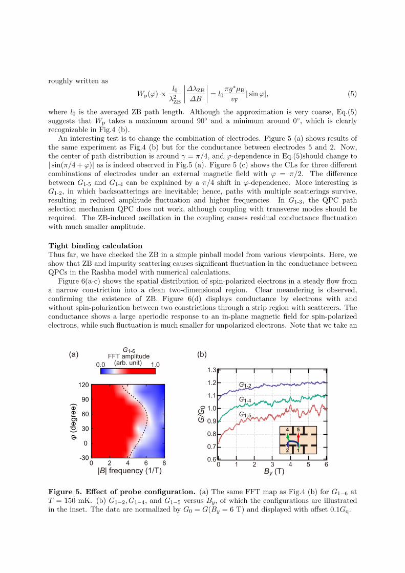
An interesting test is to change the combination of electrodes. Figure 5 (a) shows results ofthe same experiment as Fig.4 (b) but for the conductance between electrodes 5 and 2. Now,the center of path distribution is around γ = π/4, and ϕ-dependence in Eq.(5)should change to| sin(π/4 + ϕ)| as is indeed observed in Fig.5 (a). Figure 5 (c) shows the CLs for three differentcombinations of electrodes under an external magnetic field with ϕ = π/2. The differencebetween G1-5 and G1-4 can be explained by a π/4 shift in ϕ-dependence. More interesting isG1-2, in which backscatterings are inevitable; hence, paths with multiple scatterings survive,resulting in reduced amplitude fluctuation and higher frequencies. In G1-3, the QPC pathselection mechanism QPC does not work, although coupling with transverse modes should berequired. The ZB-induced oscillation in the coupling causes residual conductance fluctuationwith much smaller amplitude.
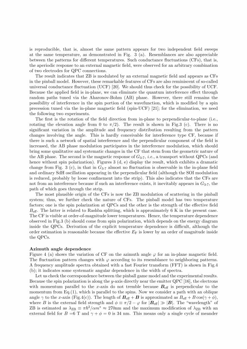
Tight binding calculationThus far, we have checked the ZB in a simple pinball model from various viewpoints. Here, weshow that ZB and impurity scattering causes significant fluctuation in the conductance betweenQPCs in the Rashba model with numerical calculations.
Figure 6(a-c) shows the spatial distribution of spin-polarized electrons in a steady flow froma narrow constriction into a clean two-dimensional region. Clear meandering is observed,confirming the existence of ZB. Figure 6(d) displays conductance by electrons with andwithout spin-polarization between two constrictions through a strip region with scatterers. Theconductance shows a large aperiodic response to an in-plane magnetic field for spin-polarizedelectrons, while such fluctuation is much smaller for unpolarized electrons. Note that we take an
(a) (b)
0 42 6 8|B| frequency (1/T)
G1-6FFT amplitude
(arb. unit) 0.0 1.0
φ (d
egre
e)
-30
120
90
60
30
0
By (T)
0.9
0.8
0.7
0.6
1.0
1.3
1.2
1.1
G/G
0
G1-5
G1-4
G1-2
0 654321
12
4 5
Figure 5. Effect of probe configuration. (a) The same FFT map as Fig.4 (b) for G1−6 atT = 150 mK. (b) G1−2, G1−4, and G1−5 versus By, of which the configurations are illustratedin the inset. The data are normalized by G0 = G(By = 6 T) and displayed with offset 0.1Gq.
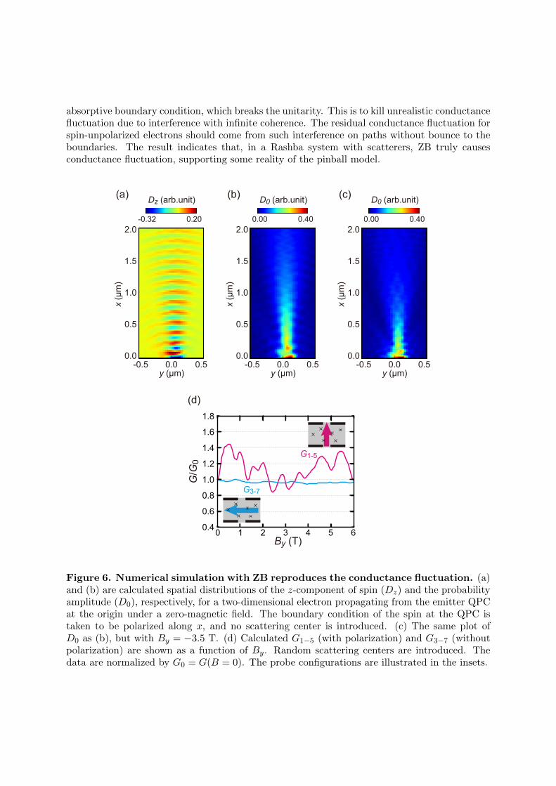
absorptive boundary condition, which breaks the unitarity. This is to kill unrealistic conductancefluctuation due to interference with infinite coherence. The residual conductance fluctuation forspin-unpolarized electrons should come from such interference on paths without bounce to theboundaries. The result indicates that, in a Rashba system with scatterers, ZB truly causesconductance fluctuation, supporting some reality of the pinball model.
(d)
By (T)6543210
G/G
0
1.0
0.8
0.6
0.4
1.2
1.4
1.6
1.8
G3-7
G1-5
Dz (arb.unit)
-0.32 0.20
-0.50.0
2.0
1.5
1.0
0.5
0.50.0y (μm)
x (μ
m)
D0 (arb.unit)
0.00 0.40
-0.50.0
2.0
1.5
1.0
0.5
0.50.0y (μm)
x (μ
m)
D0 (arb.unit)
0.00 0.40
-0.50.0
2.0
1.5
1.0
0.5
0.50.0y (μm)
x (μ
m)
(a) (b) (c)
Figure 6. Numerical simulation with ZB reproduces the conductance fluctuation. (a)and (b) are calculated spatial distributions of the z-component of spin (Dz) and the probabilityamplitude (D0), respectively, for a two-dimensional electron propagating from the emitter QPCat the origin under a zero-magnetic field. The boundary condition of the spin at the QPC istaken to be polarized along x, and no scattering center is introduced. (c) The same plot ofD0 as (b), but with By = −3.5 T. (d) Calculated G1−5 (with polarization) and G3−7 (withoutpolarization) are shown as a function of By. Random scattering centers are introduced. Thedata are normalized by G0 = G(B = 0). The probe configurations are illustrated in the insets.
MethodsTwo-dimensional electron system in an InAs quantum wellThe substrate was an InAs quantum well, grown on a (001) InP using the molecular beamepitaxy technique. It consists of, from the bottom, InAlAs and InGaAs (700 nm) as bufferlayers, InAs (4 nm), InGaAs (4 nm), InAlAs (10 nm), n-InAlAs (40 nm), InAlAs (5 nm), andInGaAs (2 nm). QPCs were fabricated by electron-beam lithography and Ar dry-etching withthe depth of 300 nm. Contacts were fabricated by AuGe deposition (100 nm) and subsequentannealing (280 degree, 5 min).
The specimen was cooled to 70 mK in a dilution fridge with a superconducting solenoid forapplying the magnetic field. A conventional lock-in technique was used for measuring two-wireconductances with frequencies lower than 1 kHz.
Setups for numerical calculationsFor numerical calculations we employed the “Kwant” package [22], which is based on a tight-binding approximation. The distance between two QPCs L = 1.8 µm, QPC width w = 400 nm,and Rashba strength α = 3.6×10⁻¹¹ eVm were adopted to simulate the experiment. The effectivemass m∗ = 0.025m0 (where m0 is the electron mass in vacuum) and g-factor g∗ = +8.6 wereadopted from previous studies [13]. EF was tuned to give the QPC conductance GQPC = 1.0Gq.The calculated area was 3.6 µm × 3.0 µm, and was surrounded by absorption walls (exceptfor the QPC passes) and simplified to a square lattice with the lattice constant a = 25 nm.Impurities were introduced by adding randomly-distributed values to onsite energy. The typicalamplitudes of the impurities were 0.2 eV.
References[1] Schrodinger, E. Uber die kraftefreie Bewegung in der relativistischen Quantenmechanik. Sitzungsber. Preuss.
Akad. Wiss. Berl. Phys.-math. Kl. 24, 418-428 (1930).[2] Zawadzki, W. and Rusin, T. M. Zitterbewegung (trembling motion) of electrons in semiconductors: a review.
J. Phys.: Condens. Matter 23, 143201 (2011).[3] Gerritsma, R. et al. Quantum simulation of the Dirac equation. Nature 463, 68-71 (2010).[4] LeBlanc, L. J. et al. Direct observation of zitterbewegung in a Bose-Einstein condensate. New J. Phys. 15,
073011 (2013).[5] Qu, C., Hamner, C., Gong, M., Zhang, C. and Engels, P. Observation of Zitterbewegung in a spin-orbit-
coupled Bose-Einstein condensate. Phys. Rev. A 88, 021604 (2013).[6] Schliemann, J., Loss, D. and Westervelt, R. M. Zitterbewegung of Electronic Wave Packets in III-V Zinc-
Blende Semiconductor Quantum Wells, Phys. Rev. Lett. 94, 206801 (2005).[7] Rusin, T. M. and Zawadzki, W. Theory of electron Zitterbewegung in graphene probed by femtosecond laser
pulses. Phys. Rev. B 80, 045416 (2009).[8] Brusheim, P. and Xu, H. Q. Spin transport and spin Hall effect in an electron waveguide in the presence of
an in-plane magnetic field and spin-orbit interaction. Phys. Rev. B 75, 195333 (2007).[9] Bychkov, Y. A. and Rashba, E. I. Properties of a 2D electron gas with lifted spectral degeneracy. JETP Lett.
39, 78-81 (1984).[10] Benter, T. et al. Quantized conductance and evidence for zitterbewegung in InAs spin filters. Appl. Phys.
Lett. 102, 212405 (2013).[11] Biswas, T. and Ghosh, T. K. Zitterbewegung of electrons in quantum wells and dots in the presence of an
in-plane magnetic field. J. Phys.: Condens. Matter 24, 185304 (2012).[12] Matsuda T. and Yoh K. Enhancement of Spin-Orbit Interaction by Bandgap Engineering in InAs-Based
Heterostructures. J. Electron. Mater. 37, 1806-1810 (2008).[13] Yang M. J., Lin-Chung P. J., Shanabrook, B. V., Waterman J. R., Wagner R. J. and Moore W. J.
Enhancement of cyclotron mass in semiconductor quantum wells. Phys. Rev. B 47, 1691-1694 (1993).[14] Yang M. J., Wagner R. J., Shanabrook B. V., Waterman J. R. and Moore W.J. Spin-resolved cyclotron
resonance in InAs quantum wells: A study of the energy-dependent g factor. Phys. Rev. B 47, 6807-6810(1993).
[15] Nitta J., Akazaki T., Takayanagi H. and Enoki T. Gate Control of Spin-Orbit Interaction in an InvertedIn0.53Ga0.47As/In0.52Al0.48As Heterostructure. Phys. Rev. Lett. 78, 1335-1338 (1997).
[16] Eto, M., Hayashi, T., Kurotani, Y. and Yokouchi, H. Spin injection using quantum point contacts withspin-orbit interaction and its detection. Phys. Stat. Sol. (c) 3, 4168-4171 (2006).
[17] S.-W. Kim, Y. Hashimoto, T. Nakamura, and S. Katsumoto Experimental Verification of a Spin-InterferenceDevice Action. Phys. Rev. B 94, 125307 (2016).
[18] Kohda, M. et al. Spin-orbit induced electronic spin separation in semiconductor nanostructures. NatureCommn. 3, 1082 (2012).
[19] Topinka, M. et al. Coherent branched flow in a two-dimensional electron gas. Nature 410, 183-186 (2001).[20] Lee P. A. and Stone A. D. Universal Conductance Fluctuations in Metals. Phys. Rev. Lett. 55, 1622-1625
(1985).[21] Scheid, M., Adagideli, I., Nitta, J. and Richter K., Anisotropic universal conductance fluctuations in
disordered quantum wires with Rashba and Dresselhaus spin-orbit interaction and an applied in-planemagnetic field. Semicond. Sci. Technol. 24, 064005 (2009).
[22] Groth, C. W., Wimmer, M., Akhmerov, R., and Waintl, X. Kwant: a software package for quantum transport.New. J. Phys. 16, 063065 (2014).
AcknowledgmentThis work was supported by a Grant-in-Aid for Scientific Research on Innovative Areas, “NanoSpin Conversion Science” (Grant No. 26103003), also by Grant No. 25247051 and by SpecialCoordination Funds for Promoting Science and Technology. Iwasaki was also supported by theJapan Society for the Promotion of Science through Program for Leading Graduate Schools(MERIT).
Author contributionsY. I. fabricated the sample and performed measurements. Y. H grew and provided the substrate.Y. I, T. N and S. K discussed the results and derived the theoretical model. Y. I and S. K wrotethe manuscript.