Embed Size (px)
Citation preview

IN
EN NC
OUT1 5
4310µF0.1µF
VIN = 3.3V
10µF
MBR0520L
MBR0520L
1:2.2
10µF
3
1
D2
SN6501
D1
Vcc
5
2
GND
GND
4 VOUT-REG = 5V
TPS76350
2GND
VOUT
SN6501www.ti.com SLLSEA0F –FEBRUARY 2012–REVISED AUGUST 2013
Transformer Driver for Isolated Power SuppliesCheck for Samples: SN6501
1FEATURES APPLICATIONS• Push-Pull Driver for Small Transformers • Isolated Interface Power Supply for CAN, RS-
485, RS-422, RS-232, SPI, I2C, Low-Power LAN• Single 3.3 V or 5 V Supply• Industrial Automation• High Primary-side Current Drive:• Process Control– 5 V Supply: 350 mA (max)• Medical Equipment– 3.3 V Supply: 150 mA (max)
• Low Ripple on Rectified Output Permits SmallOutput Capacitors
• Small 5-pin SOT23 Package
DESCRIPTIONThe SN6501 is a monolithic oscillator/power-driver, specifically designed for small form factor, isolated powersupplies in isolated interface applications. It drives a low-profile, center-tapped transformer primary from a 3.3 Vor 5 V DC power supply. The secondary can be wound to provide any isolated voltage based on transformerturns ratio.
The SN6501 consists of an oscillator followed by a gate drive circuit that provides the complementary outputsignals to drive the ground referenced N-channel power switches. The internal logic ensures break-before-makeaction between the two switches.
The SN6501 is available in a small SOT23-5 package, and is specified for operation at temperatures from –40°Cto 125°C.
Figure 1. Typical Operating Circuit
1
Please be aware that an important notice concerning availability, standard warranty, and use in critical applications ofTexas Instruments semiconductor products and disclaimers thereto appears at the end of this data sheet.
PRODUCTION DATA information is current as of publication date. Copyright © 2012–2013, Texas Instruments IncorporatedProducts conform to specifications per the terms of the TexasInstruments standard warranty. Production processing does notnecessarily include testing of all parameters.

50W
VIN
10µF
3
1
SN6501
5
2
4D2
D1
VCC
GND
GND50W
1 5
2
3 4
D1
VCC
D2
GND
GND
OSC
Q
Q
SN6501
Gate
Drive
D1
VCC
D2
GNDGND
SN6501SLLSEA0F –FEBRUARY 2012–REVISED AUGUST 2013 www.ti.com
These devices have limited built-in ESD protection. The leads should be shorted together or the device placed in conductive foamduring storage or handling to prevent electrostatic damage to the MOS gates.
FUNCTIONAL BLOCK DIAGRAM
PIN FUNCTIONS
PIN No. NAME DESCRIPTION1 D1 Drain 12 Vcc Supply voltage3 D2 Drain 2
4,5 GND Ground
SPACER
SPACER
TEST CIRCUIT
Figure 2. Test Circuit for RON, fSW, fSt, tr-D, tf-D, tBBM
2 Submit Documentation Feedback Copyright © 2012–2013, Texas Instruments Incorporated
Product Folder Links :SN6501

SN6501www.ti.com SLLSEA0F –FEBRUARY 2012–REVISED AUGUST 2013
ABSOLUTE MAXIMUM RATINGSover operating free-air temperature range (unless otherwise noted) (1)
VALUESVCC Supply voltage –0.3 V to +6 VVD1, VD2 Output switch voltage 14 VID1P, ID2P Peak output switch current 500 mAPTOT Continuous power dissipation 250 mW
Human Body Model ESDA/JEDEC JS-001-2012 ±4 kVESD Charged Device Model JEDEC JESD22-C101E All Pins ±1.5 kV
Machine Model JEDEC JESD22-A115-A ±200 VTSTG Storage temperature range –65°C to 150°CTJ Junction temperature 170°C
(1) Stresses beyond those listed under ABSOLUTE MAXIMUM RATINGS cause permanent damage to the device. These are stress ratingsonly and functional operation of the device at these or any other conditions beyond those indicated under RECOMMENDEDOPERATING CONDITIONS is not implied. Exposure to absolute-maximum-rated conditions for extended periods affects devicereliability.
THERMAL INFORMATIONSN6501
THERMAL METRIC (1) UNITSDBV 5-PINS
θJA Junction-to-ambient thermal resistance 208.3θJCtop Junction-to-case (top) thermal resistance 87.1θJB Junction-to-board thermal resistance 40.4
°C/WψJT Junction-to-top characterization parameter 5.2ψJB Junction-to-board characterization parameter 39.7θJCbot Junction-to-case (bottom) thermal resistance N/A
(1) For more information about traditional and new thermal metrics, see the IC Package Thermal Metrics application report, SPRA953.
need space between thermal table note and ROC title
RECOMMENDED OPERATING CONDITIONSMIN TYP MAX UNIT
VCC Supply voltage 3 5.5 VVCC = 5 V ± 10%, 0 11When connected to Transformer withVD1, VD2 Output switch voltage Vprimary winding Center-tappedVCC = 3.3 V ± 10% 0 7.2
VD1, VD2 Swing ≥ 3.8 V,VCC = 5 V ± 10% 350see Figure 58 for typical characteristicsD1 and D2 output switchID1, ID2 mAcurrent – Primary-side VD1, VD2 Swing ≥ 2.5 V,VCC = 3.3 V ± 10% 150see Figure 57 for typical characteristicsTA Ambient temperature –40 125 °C
Copyright © 2012–2013, Texas Instruments Incorporated Submit Documentation Feedback 3
Product Folder Links :SN6501

SN6501SLLSEA0F –FEBRUARY 2012–REVISED AUGUST 2013 www.ti.com
ELECTRICAL CHARACTERISTICSOver full-range of recommended operating conditions, unless otherwise noted
PARAMETER TEST CONDITIONS MIN TYP MAX UNITVCC = 3.3 V ± 10%, See Figure 2 1 3
RON Switch-on resistance ΩVCC = 5 V ± 10%, See Figure 2 0.6 2VCC = 3.3 V ± 10%, no load 150 400
ICC Average supply current (1) uAVCC = 5 V ± 10%, no load 300 700
fST Startup frequency VCC = 2.4 V, See Figure 2 300 kHzVCC = 3.3 V ± 10%, See Figure 2 250 360 550
fSW D1, D2 Switching frequency kHzVCC = 5 V ± 10%, See Figure 2 300 410 620VCC = 3.3 V ± 10%, See Figure 2 70
tr-D D1, D2 output rise time nsVCC = 5 V ± 10%, See Figure 2 80VCC = 3.3 V ± 10%, See Figure 2 110
tf-D D1, D2 output fall time nsVCC = 5 V ± 10%, See Figure 2 60VCC = 3.3 V ± 10%, See Figure 2 150
tBBM Break-before-make time nsVCC = 5 V ± 10%, See Figure 2 50
(1) Average supply current is the current used by SN6501 only. It does not include load current.
4 Submit Documentation Feedback Copyright © 2012–2013, Texas Instruments Incorporated
Product Folder Links :SN6501

TP1
0
10
20
30
40
50
60
70
80
90
Eff
icie
ncy -
%
I - mALOAD
0 10 20 30 40 50 60 70 9080 100
T1 = (Wurth Electronics Midcom)V = 3.3 V, V = 5 V
Unregulated outputIN OUT
760390013
V-
VO
UT
I - mALOAD
TP1
0
1
2
3
4
5
6
0 10 20 30 40 50 60 70 9080 100
T1 = (Wurth Electronics Midcom)V = 3.3 V, V = 5 V
Unregulated output
760390013
IN OUT
TP1
0
10
20
30
40
50
60
70
80
90E
ffic
ien
cy -
%
I - mALOAD
0 10 20 30 40 50 60 70 9080 100
T1 = (Wurth Electronics Midcom)V = 3.3 V, V = 3.3 V
Unregulated output
760390011
IN OUT
V-
VO
UT
I - mALOAD
TP1
0
1
2
3
4
5
6
0 10 20 30 40 50 60 70 9080 100
T1 = (Wurth Electronics Midcom)V = 3.3 V, V = 3.3 V
Unregulated output
760390011
IN OUT
0
10
20
30
40
50
60
70
80
90
Eff
icie
nc
y -
%
TP1
0 10 20 30 40 50 60 70 80 90 100
T1 = (Wurth Electronics Midcom)V = 5 V, V = 5 V
Unregulated outputIN OUT
760390012
I - mALOAD
V-
VO
UT
TP1
I - mALOAD
0
1
2
3
4
5
6
0 10 20 30 40 50 60 70 80 90 100
T1 = (Wurth Electronics Midcom)V = 5 V, V = 5 V
Unregulated output
760390012
IN OUT
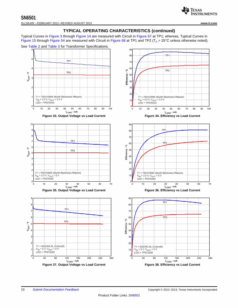
SN6501www.ti.com SLLSEA0F –FEBRUARY 2012–REVISED AUGUST 2013
TYPICAL OPERATING CHARACTERISTICSTypical Curves in Figure 3 through Figure 14 are measured with Circuit in Figure 67 at TP1; whereas, Typical Curves inFigure 15 through Figure 54 are measured with Circuit in Figure 68 at TP1 and TP2 (TA = 25°C unless otherwise noted).
See Table 2 and Table 3 for Transformer Specifications.
Figure 3. Output Voltage vs. Load Current Figure 4. Efficiency vs Load Current
Figure 5. Output Voltage vs Load Current Figure 6. Efficiency vs Load Current
Figure 7. Output Voltage vs Load Current Figure 8. Efficiency vs Load Current
Copyright © 2012–2013, Texas Instruments Incorporated Submit Documentation Feedback 5
Product Folder Links :SN6501

0 10 30 100
I - mALOAD
0
10
20
30
40
50
60
70
80
90
Eff
icie
nc
y -
%
TP1
20 40 50 60 70 80 90
T1 = 750313769 (Wurth Electronics Midcom)V = 3.3 V, V = 5 V
Uregulated outputIN OUT
V-
VO
UT
TP1
I - mALOAD
0
1
2
3
4
5
6
0 10 20 30 40 50 60 70 80 90 100
T1 = (Wurth Electronics Midcom)V = 3.3 V, V = 5 V
Unregulated output
750313769
IN OUT
0 10 30 100
I - mALOAD
0
10
20
30
40
50
60
70
80
90E
ffic
ien
cy
- %
TP1
20 40 50 60 70 80 90
T1 = 750313734 (Wurth Electronics Midcom)V = 3.3 V, V = 3.3 V
Uregulated outputIN OUT
V-
VO
UT
TP1
I - mALOAD
0
1
2
3
4
5
6
0 10 20 30 40 50 60 70 80 90 100
T1 = (Wurth Electronics Midcom)V = 3.3 V, V = 3.3 V
Unregulated output
750313734
IN OUT
0
I - mALOAD
0
10
20
30
40
50
60
70
80
90
Eff
icie
nc
y -
%
TP1
T1 = 750313734 (Wurth Electronics Midcom)V = 5 V, V = 5 V
Uregulated outputIN OUT
10 30 10020 40 50 60 70 80 90
V-
VO
UT
TP1
I - mALOAD
0
1
2
3
4
5
6
0 10 20 30 40 50 60 70 80 90 100
T1 = (Wurth Electronics Midcom)V = 5 V, V = 5 V
Unregulated output
750313734
IN OUT
SN6501SLLSEA0F –FEBRUARY 2012–REVISED AUGUST 2013 www.ti.com
TYPICAL OPERATING CHARACTERISTICS (continued)Typical Curves in Figure 3 through Figure 14 are measured with Circuit in Figure 67 at TP1; whereas, Typical Curves inFigure 15 through Figure 54 are measured with Circuit in Figure 68 at TP1 and TP2 (TA = 25°C unless otherwise noted).
See Table 2 and Table 3 for Transformer Specifications.
Figure 9. Output Voltage vs Load Current Figure 10. Efficiency vs Load Current
Figure 11. Output Voltage vs Load Current Figure 12. Efficiency vs Load Current
Figure 13. Output Voltage vs Load Current Figure 14. Efficiency vs Load Current
6 Submit Documentation Feedback Copyright © 2012–2013, Texas Instruments Incorporated
Product Folder Links :SN6501

0 10 30 100
I - mALOAD
0
10
20
30
40
50
60
70
80
90
Eff
icie
nc
y -
%
TP1
20 40 50 60 70 80 90
T1 = 750313710 (Wurth Electronics Midcom)V = 5 V, V = 3.3 V
LDO = TPS76333IN OUT
TP2
V-
VO
UT
TP1
I - mALOAD
0
1
2
3
4
5
6
0 10 20 30 40 50 60 70 80 90 100
T1 = (Wurth Electronics Midcom)V = 5 V, V = 3.3 V
LDO = TPS76333
750313710
IN OUT
TP2
V-
VO
UT
I - mALOAD
TP1
0
1
2
3
4
5
6
0 10 20 30 40 50 60 70 9080 100
T1 = (Wurth Electronics Midcom)V = 3.3 V, V = 3.3 V
LDO = TPS76333IN OUT
760390014
TP2
0
10
20
30
40
50
60
70
80
90E
ffic
ien
cy
- %
TP2
0 10 20 30 40 50 60 70 80 90 100
T1 = (Wurth Electronics Midcom)V = 3.3 V, V = 3.3 V
LDO = TPS763333
760390014
IN OUT
TP1
I - mALOAD
0
1
2
3
4
5
6
7
8
V-
VO
UT
I - mALOAD
TP1
TP2
0 10 20 30 40 50 60 70 9080 100
T1 = (Wurth Electronics Midcom)V = 5 V, V = 5 V
LDO = TPS73250IN OUT
760390014
I - mALOAD
TP1
TP2
0
10
20
30
40
50
60
70
80
90
Eff
icie
ncy -
%
0 10 20 30 40 50 60 70 9080 100
T1 = (Wurth Electronics Midcom)V = 5 V, V = 5 V
LDO = TPS73250IN OUT
760390014
SN6501www.ti.com SLLSEA0F –FEBRUARY 2012–REVISED AUGUST 2013
TYPICAL OPERATING CHARACTERISTICS (continued)Typical Curves in Figure 3 through Figure 14 are measured with Circuit in Figure 67 at TP1; whereas, Typical Curves inFigure 15 through Figure 54 are measured with Circuit in Figure 68 at TP1 and TP2 (TA = 25°C unless otherwise noted).
See Table 2 and Table 3 for Transformer Specifications.
Figure 15. Output Voltage vs Load Current Figure 16. Efficiency vs Load Current
Figure 17. Output Voltage vs Load Current Figure 18. Efficiency vs Load Current
Figure 19. Output Voltage vs Load Current Figure 20. Efficiency vs Load Current
Copyright © 2012–2013, Texas Instruments Incorporated Submit Documentation Feedback 7
Product Folder Links :SN6501

0 10 30 100
I - mALOAD
0
10
20
30
40
50
60
70
80
90
Eff
icie
nc
y -
%
TP1
20 40 50 60 70 80 90
T1 = 750313638 (Wurth Electronics Midcom)V = 3.3 V, V = 3.3 V
LDO = TPS76333IN OUT
TP2
V-
VO
UT
TP1
I - mALOAD
0
1
2
3
4
5
6
0 10 20 30 40 50 60 70 80 90 100
TP2
T1 = (Wurth Electronics Midcom)V = 3.3 V, V = 3.3 V
LDO = TPS76333
750313638
IN OUT
0 10 30 100
I - mALOAD
0
10
20
30
40
50
60
70
80
90E
ffic
ien
cy
- %
TP1
20 40 50 60 70 80 90
T1 = 750313638 (Wurth Electronics Midcom)V = 5 V, V = 5 V
LDO = TPS73250IN OUT
TP2
V-
VO
UT
TP1
I - mALOAD
0
1
2
3
4
5
8
0 10 20 30 40 50 60 70 80 90 100
TP2
T1 = (Wurth Electronics Midcom)V = 5 V, V = 5 V
LDO = TPS73250
750313638
IN OUT
7
6
0
1
2
3
4
5
6
7
8
V-
VO
UT
I - mALOAD
TP2
TP1
0 10 20 30 40 50 60 70 9080 100
T1 = (Wurth Electronics Midcom)V = 3.3 V, V = 5 V
LDO = TPS76350IN OUT
760390015
0
10
20
30
40
50
60
70
80
90
Eff
icie
nc
y -
%
0 10 20 30 40 50 60 70 80 90 100
I - mALOAD
T1 = (Wurth Electronics Midcom)V = 3.3 V, V = 5 V
LDO = TPS76350
760390015
IN OUT
TP1
TP2
SN6501SLLSEA0F –FEBRUARY 2012–REVISED AUGUST 2013 www.ti.com
TYPICAL OPERATING CHARACTERISTICS (continued)Typical Curves in Figure 3 through Figure 14 are measured with Circuit in Figure 67 at TP1; whereas, Typical Curves inFigure 15 through Figure 54 are measured with Circuit in Figure 68 at TP1 and TP2 (TA = 25°C unless otherwise noted).
See Table 2 and Table 3 for Transformer Specifications.
Figure 21. Output Voltage vs Load Current Figure 22. Efficiency vs Load Current
Figure 23. Output Voltage vs Load Current Figure 24. Efficiency vs Load Current
Figure 25. Output Voltage vs Load Current Figure 26. Efficiency vs Load Current
8 Submit Documentation Feedback Copyright © 2012–2013, Texas Instruments Incorporated
Product Folder Links :SN6501

0 40 80 120 160 200 240I - mALOAD
V-
VO
UT
0
1
2
3
4
5
6
7
8
TP1
TP2
T1 = (750310999 )Wurth Electronics Midcom
VIN = 5 V, VOUT = 5 V
LDO = TPS73250
0 40 80 120 160 200 240I - mALOAD
0
10
20
30
40
50
60
70
80TP1
TP2
Eff
icie
ncy -
%
90
T1 = ( )750310999 Wurth Electronics Midcom
V = 5 V, VIN OUT = 5 V
LDO = TPS73250
0 10 30 100
I - mALOAD
0
10
20
30
40
50
60
70
80
90E
ffic
ien
cy
- %
TP1
20 40 50 60 70 80 90
T1 = 750313626 (Wurth Electronics Midcom)V = 3.3 V, V = 5 V
LDO = TPS76350IN OUT
TP2
V-
VO
UT
TP1
I - mALOAD
0
1
2
3
4
5
8
0 10 20 30 40 50 60 70 80 90 100
TP2
T1 = (Wurth Electronics Midcom)V = 3.3 V, V = 5 V
LDO = TPS76350
750313626
IN OUT
7
6
0 10 30 100
I - mALOAD
0
10
20
30
40
50
60
70
80
90
Eff
icie
nc
y -
%
TP1
20 40 50 60 70 80 90
T1 = 750313638 (Wurth Electronics Midcom)V = 5 V, V = 3.3 V
LDO = TPS76333IN OUT
TP2
V-
VO
UT
TP1
I - mALOAD
0
1
2
3
4
5
6
0 10 20 30 40 50 60 70 80 90 100
T1 = (Wurth Electronics Midcom)V = 5 V, V = 3.3 V
LDO = TPS76333
750313638
IN OUT
TP2
SN6501www.ti.com SLLSEA0F –FEBRUARY 2012–REVISED AUGUST 2013
TYPICAL OPERATING CHARACTERISTICS (continued)Typical Curves in Figure 3 through Figure 14 are measured with Circuit in Figure 67 at TP1; whereas, Typical Curves inFigure 15 through Figure 54 are measured with Circuit in Figure 68 at TP1 and TP2 (TA = 25°C unless otherwise noted).
See Table 2 and Table 3 for Transformer Specifications.
Figure 27. Output Voltage vs Load Current Figure 28. Efficiency vs Load Current
Figure 29. Output Voltage vs Load Current Figure 30. Efficiency vs Load Current
Figure 31. Output Voltage vs Load Current Figure 32. Efficiency vs Load Current
Copyright © 2012–2013, Texas Instruments Incorporated Submit Documentation Feedback 9
Product Folder Links :SN6501
0
1
2
3
4
5
6
7
8
9
V-
VO
UT
TP1
TP2
0 40 80 120 160 200 240 280
I - mALOAD
T1 = (Coilcraft)V = 5 V, V = 5 V
LDO = TPS73250IN OUT
DA2303-AL
0 40 80 120 160 200 240 280
I - mALOAD
0
10
20
30
40
50
60
70
80
90
Eff
icie
nc
y -
%
TP1
TP2
T1 = (Coilcraft)V = 5 V, V = 5 V
LDO = TPS73250IN OUT
DA2303-AL
0 10 20 30 40 50 60 70I - mALOAD
V-
VO
UT
0
1
2
3
4
5
6
7
8
9
10
TP1
TP2
T1 = ( )750310995 Wurth Electronics Midcom
V = 3.3 V, VIN OUT = 5 V
LDO = TPS76350
0
10
20
30
40
50
60
70
80
90E
ffic
ien
cy -
%
0 10 20 30 40 50 60 70I - mALOAD
TP1
TP2
T1 = ( )750310995 Wurth Electronics Midcom
VIN = 3.3 V, V = 5 VOUT
LDO = TPS76350
0 20 40 60 70 90 100
I - mALOAD
0
10
20
30
40
50
60
70
80
Eff
icie
ncy -
%
90
10 30 50 80
TP1
TP2
T1 = ( )750310999 Wurth Electronics Midcom
V = 3.3 V, VIN OUT = 3.3 V
LDO = TPS76333
0 10 40 60 70 90 100
I - mALOAD
V-
VO
UT
0
1
2
3
4
5
6
TP1
TP2
805020 30
T1 = ( )750310999 Wurth Electronics Midcom
V = 3.3 V, VIN OUT = 3.3 V
LDO = TPS76333
SN6501SLLSEA0F –FEBRUARY 2012–REVISED AUGUST 2013 www.ti.com
TYPICAL OPERATING CHARACTERISTICS (continued)Typical Curves in Figure 3 through Figure 14 are measured with Circuit in Figure 67 at TP1; whereas, Typical Curves inFigure 15 through Figure 54 are measured with Circuit in Figure 68 at TP1 and TP2 (TA = 25°C unless otherwise noted).
See Table 2 and Table 3 for Transformer Specifications.
Figure 33. Output Voltage vs Load Current Figure 34. Efficiency vs Load Current
Figure 35. Output Voltage vs Load Current Figure 36. Efficiency vs Load Current
Figure 37. Output Voltage vs Load Current Figure 38. Efficiency vs Load Current
10 Submit Documentation Feedback Copyright © 2012–2013, Texas Instruments Incorporated
Product Folder Links :SN6501

0
1
2
3
4
5
6
7
8
9
V-
VO
UT
I - mALOAD
0 10 20 30 40 50 60 70 80
TP1
TP2
T1 = (Coilcraft)V = 3.3 V, V = 5 V
LDO = TPS76350IN OUT
MA5632-AL
I - mALOAD
0 10 20 30 40 50 60 70 80
T1 = (Coilcraft)V = 3.3 V, V = 5 V
LDO = TPS76350IN OUT
MA5632-AL
TP1
TP2
0
10
20
30
40
50
60
70
80
90
Eff
icie
ncy -
%
0 10 20 30 40 50 60 700
1
2
3
4
5
6
7
8
9
V-
VO
UT
I - mALOAD
TP1
TP2
T1 = (Coilcraft)V = 3.3 V, V = 5 V
LDO = TPS76350IN OUT
DA2304-AL
0
10
20
30
40
50
60
70
80
90E
ffic
ien
cy
- %
I - mALOAD
0 10 20 30 40 50 60 70 80
TP1
TP2
T1 = (Coilcraft)V = 3.3 V, V = 5 V
LDO = TPS76350IN OUT
DA2304-AL
T1 = (Coilcraft)V = 3.3 V, V = 3.3 V
LDO = TPS76333IN OUT
DA2303-AL
0
1
2
3
4
5
6
7
8
9
V-
VO
UT
0 20 40 60 80 100
I - mALOAD
TP2
TP1
TP1
TP2
0
10
20
30
40
50
60
70
80
90
Eff
icie
ncy -
%
0 20 40 60 80 100 120I - mALOAD
T1 = (Coilcraft)V = 3.3 V, V = 3.3 V
LDO = TPS76333IN OUT
DA2303-AL
SN6501www.ti.com SLLSEA0F –FEBRUARY 2012–REVISED AUGUST 2013
TYPICAL OPERATING CHARACTERISTICS (continued)Typical Curves in Figure 3 through Figure 14 are measured with Circuit in Figure 67 at TP1; whereas, Typical Curves inFigure 15 through Figure 54 are measured with Circuit in Figure 68 at TP1 and TP2 (TA = 25°C unless otherwise noted).
See Table 2 and Table 3 for Transformer Specifications.
Figure 39. Output Voltage vs Load Current Figure 40. Efficiency vs Load Current
Figure 41. Output Voltage vs Load Current Figure 42. Efficiency vs Load Current
Figure 43. Output Voltage vs Load Current Figure 44. Efficiency vs Load Current
Copyright © 2012–2013, Texas Instruments Incorporated Submit Documentation Feedback 11
Product Folder Links :SN6501

0
10
20
30
40
50
60
70
80
90
Eff
icie
nc
y -
%
0 10 20 30 40 50 60 70I - mALOAD
TP1
TP2
T1 = (Murata)V = 3.3 V, V = 5 V
LDO = TPS76350IN OUT
78253/35MC
0
1
2
3
4
5
6
7
8
V-
VO
UT
0 10 20 30 40 50 60 70I - mALOAD
TP1
TP2
T1 = (Murata)V = 3.3 V, V = 5 V
LDO = TPS76350IN OUT
78253/35MC
0
10
20
30
40
50
60
70
80
90E
ffic
ien
cy -
%
I - mALOAD
0 10 20 30 40 50 60 70 80 90 100 110 120
TP1
TP2
T1 = (Murata)V = 3.3 V, V = 3.3 V
LDO = TPS76333IN OUT
78253/55MC
0
1
2
3
4
5
6
7
8
V-
VO
UT
I - mALOAD
0 10 20 30 40 50 60 70 80 90 100 110 120
TP2
TP1
T1 = (Murata)V = 3.3 V, V = 3.3 V
LDO = TPS76333IN OUT
78253/55MC
I - mALOAD
0 20 40 60 80 100 120 140 160 180 200
TP1
TP2
0
1
2
3
4
5
6
7
8
V-
VO
UT
T1 = (Murata)V = 5 V, V = 5 V
LDO = TPS73250IN OUT
78253/55MC
0
10
20
30
40
50
60
70
80
90
Eff
icie
ncy -
%
I - mALOAD
0 20 40 60 80 100 120 140 160 180 200
TP2
TP1
T1 = (Murata)V = 5 V, V = 5 V
LDO = TPS73250IN OUT
78253/55MC
SN6501SLLSEA0F –FEBRUARY 2012–REVISED AUGUST 2013 www.ti.com
TYPICAL OPERATING CHARACTERISTICS (continued)Typical Curves in Figure 3 through Figure 14 are measured with Circuit in Figure 67 at TP1; whereas, Typical Curves inFigure 15 through Figure 54 are measured with Circuit in Figure 68 at TP1 and TP2 (TA = 25°C unless otherwise noted).
See Table 2 and Table 3 for Transformer Specifications.
Figure 45. Output Voltage vs Load Current Figure 46. Efficiency vs Load Current
Figure 47. Output Voltage vs Load Current Figure 48. Efficiency vs Load Current
Figure 49. Output Voltage vs Load Current Figure 50. Efficiency vs Load Current
12 Submit Documentation Feedback Copyright © 2012–2013, Texas Instruments Incorporated
Product Folder Links :SN6501

-55 -35 -15 5 25 45 65 85 105 125
T - Free-Air Temperature - °CA
0
50
100
150
200
250
300
350
I-
AC
Cm
V = 5 VCC
V = 3.3 VCC
-55 -35 -15 5 25 45 65 85 105 125
T - Free-Air Temperature - °CA
320
340
360
380
400
420
440
460
V = 5 VCC
V = 3.3 VCC
f -
Fre
qu
en
cy -
kH
zE
ffic
ien
cy -
%
TP1
0 10 20 30 40 50 60 70 80 90 100
I - mALOAD
0
TP2
T1 = (Murata)V = 3.3 V, V = 3.3 V
LDO = TPS76333
76253/55ENC
IN OUT10
20
30
40
50
60
70
80
90
V-
VO
UT
TP1
0 10 20 30 40 50 60 70 80 90 100
I - mALOAD
0
1
2
3
4
5
6
TP2
T1 = (Murata)V = 3.3 V, V = 3.3 V
LDO = TPS76333
76253/55ENC
IN OUT
Eff
icie
ncy -
%
TP1
0 20 40 60 80 100 120 140 160 180 200
I - mALOAD
0
TP2
T1 = (Murata)V = 5 V, V = 5 V
LDO = TPS73250
76253/55ENC
IN OUT10
20
30
40
50
60
70
80
90
V-
VO
UT
TP1
0 20 40 60 80 100 120 140 160 180 200
I - mALOAD
0
1
2
3
4
5
6
7
8
TP2
T1 = (Murata)V = 5 V, V = 5 V
LDO = TPS73250IN OUT
76253/55ENC
SN6501www.ti.com SLLSEA0F –FEBRUARY 2012–REVISED AUGUST 2013
TYPICAL OPERATING CHARACTERISTICS (continued)Typical Curves in Figure 3 through Figure 14 are measured with Circuit in Figure 67 at TP1; whereas, Typical Curves inFigure 15 through Figure 54 are measured with Circuit in Figure 68 at TP1 and TP2 (TA = 25°C unless otherwise noted).
See Table 2 and Table 3 for Transformer Specifications.
Figure 51. Output Voltage vs Load Current Figure 52. Efficiency vs Load Current
Figure 53. Output Voltage vs Load Current Figure 54. Efficiency vs Load Current
Figure 55. Average Supply Current vs Free-Air Temperature Figure 56. D1, D2 Switching Frequency vs Free-AirTemperature
Copyright © 2012–2013, Texas Instruments Incorporated Submit Documentation Feedback 13
Product Folder Links :SN6501

D1
500 mV/div
D2
Time - 200 ns/div
500 mV/div
V = 3.3 VCC
D1
D2
2 V/div
2 V/div
Time - 400 ns/div
V = 3.3 VCC
0 50 100 150 200
I , I - mAD1 D2
3
3.05
3.1
3.15
3.2
3.25
3.3
V, V
Vo
ltag
e S
win
g -
VD
1D
2
V = 3.3 VCC
I , I - mAD1 D2
V,
VV
olt
ag
e S
win
g -
VD
1D
2
4.55
4.6
4.65
4.7
4.75
4.8
4.85
4.9
4.95
5
0 100 200 300 400
V = 5 VCC
SN6501SLLSEA0F –FEBRUARY 2012–REVISED AUGUST 2013 www.ti.com
TYPICAL OPERATING CHARACTERISTICS (continued)Typical Curves in Figure 3 through Figure 14 are measured with Circuit in Figure 67 at TP1; whereas, Typical Curves inFigure 15 through Figure 54 are measured with Circuit in Figure 68 at TP1 and TP2 (TA = 25°C unless otherwise noted).
See Table 2 and Table 3 for Transformer Specifications.
Figure 57. D1, D2 Primary-side Output Switch Voltage Figure 58. D1, D2 Primary-side Output Switch VoltageSwing vs Current Swing vs Current
Figure 59. D1, D2 Switching Waveforms Figure 60. D1, D2 Break-Before-Make Waveform
14 Submit Documentation Feedback Copyright © 2012–2013, Texas Instruments Incorporated
Product Folder Links :SN6501

fOSC
S
S
G1
G2
Q1
Q2
Vcc
GNDGND
D2
SN6501
D1S
S
G2
G1
fOSC Freq.
DividerOSC
BBM
LogicQ1
Q2
Q1 on Q2 on
Q2 off
tBBM
Q1 off
SN6501www.ti.com SLLSEA0F –FEBRUARY 2012–REVISED AUGUST 2013
APPLICATION INFORMATIONThe SN6501 is a transformer driver designed for low-cost, small form-factor, isolated DC-DC converters utilizingthe push-pull topology. The device includes an oscillator that feeds a gate-drive circuit. The gate-drive,comprising a frequency divider and a break-before-make (BBM) logic, provides two complementary outputsignals which alternately turn the two output transistors on and off.
Figure 61. SN6501 Block Diagram and Output Timing with Break-Before-Make Action
The output frequency of the oscillator is divided down by an asynchronous divider that provides twocomplementary output signals, S and S, with a 50% duty cycle. A subsequent break-before-make logic inserts adead-time between the high-pulses of the two signals. The resulting output signals, G1 and G2, present the gate-drive signals for the output transistors Q1 and Q2. As shown in Figure 62, before either one of the gates canassume logic high, there must be a short time period during which both signals are low and both transistors arehigh-impedance. This short period, known as break-before-make time, is required to avoid shorting out both endsof the primary.
Figure 62. Detailed Output Signal Waveforms
PUSH-PULL CONVERTERPush-pull converters require transformers with center-taps to transfer power from the primary to the secondary(see Figure 63).
Copyright © 2012–2013, Texas Instruments Incorporated Submit Documentation Feedback 15
Product Folder Links :SN6501

RDS
B
H
A
A’VIN VP
VDS
VIN= VP+VDS
C
CR1
CR2
Q1Q2
VIN
VOUT
RL C
CR1
CR2
Q1Q2
VIN
VOUT
RL
SN6501SLLSEA0F –FEBRUARY 2012–REVISED AUGUST 2013 www.ti.com
Figure 63. Switching Cycles of a Push-Pull Converter
When Q1 conducts, VIN drives a current through the lower half of the primary to ground, thus creating a negativevoltage potential at the lower primary end with regards to the VIN potential at the center-tap.
At the same time the voltage across the upper half of the primary is such that the upper primary end is positivewith regards to the center-tap in order to maintain the previously established current flow through Q2, which nowhas turned high-impedance. The two voltage sources, each of which equaling VIN, appear in series and cause avoltage potential at the open end of the primary of 2×VIN with regards to ground.
Per dot convention the same voltage polarities that occur at the primary also occur at the secondary. Thepositive potential of the upper secondary end therefore forward biases diode CR1. The secondary current startingfrom the upper secondary end flows through CR1, charges capacitor C, and returns through the load impedanceRL back to the center-tap.
When Q2 conducts, Q1 goes high-impedance and the voltage polarities at the primary and secondary reverse.Now the lower end of the primary presents the open end with a 2×VIN potential against ground. In this case CR2is forward biased while CR1 is reverse biased and current flows from the lower secondary end through CR2,charging the capacitor and returning through the load to the center-tap.
CORE MAGNETIZATIONFigure 64 shows the ideal magnetizing curve for a push-pull converter with B as the magnetic flux density and Has the magnetic field strength. When Q1 conducts the magnetic flux is pushed from A to A’, and when Q2conducts the flux is pulled back from A’ to A. The difference in flux and thus in flux density is proportional to theproduct of the primary voltage, VP, and the time, tON, it is applied to the primary: B ≈ VP × tON.
Figure 64. Core Magnetization and Self-Regulation Through Positive Temperature Coefficient of RDS(on)
This volt-seconds (V-t) product is important as it determines the core magnetization during each switching cycle.If the V-t products of both phases are not identical, an imbalance in flux density swing results with an offset fromthe origin of the B-H curve. If balance is not restored, the offset increases with each following cycle and thetransformer slowly creeps toward the saturation region.
16 Submit Documentation Feedback Copyright © 2012–2013, Texas Instruments Incorporated
Product Folder Links :SN6501

SN6501www.ti.com SLLSEA0F –FEBRUARY 2012–REVISED AUGUST 2013
Fortunately, due to the positive temperature coefficient of a MOSFET’s on-resistance, the output FETs of theSN6501 have a self-correcting effect on V-t imbalance. In the case of a slightly longer on-time, the prolongedcurrent flow through a FET gradually heats the transistor which leads to an increase in RDS-on. The higherresistance then causes the drain-source voltage, VDS, to rise. Because the voltage at the primary is thedifference between the constant input voltage, VIN, and the voltage drop across the MOSFET, VP = VIN – VDS, VPis gradually reduced and V-t balance restored.
CONVERTER DESIGNThe following recommendations on components selection focus on the design of an efficient push-pull converterwith high current drive capability. Contrary to popular belief, the output voltage of the unregulated converteroutput drops significantly over a wide range in load current. The characteristic curve in Figure 41 for exampleshows that the difference between VOUT at minimum load and VOUT at maximum load exceeds a transceiver’ssupply range. Therefore, in order to provide a stable, load independent supply while maintaining maximumpossible efficiency the implementation of a low dropout regulator (LDO) is strongly advised.
The final converter circuit is shown in Figure 68. The measured VOUT and efficiency characteristics for theregulated and unregulated outputs are shown in Figure 37 to Figure 36.
SN6501 DRIVE CAPABILITYThe SN6501 transformer driver is designed for low-power push-pull converters with input and output voltages inthe range of 3 V to 5.5 V. While converter designs with higher output voltages are possible, care must be takenthat higher turns ratios don’t lead to primary currents that exceed the SN6501 specified current limits.
LDO SELECTIONThe minimum requirements for a suitable low dropout regulator are:• Its current drive capability should slightly exceed the specified load current of the application to prevent the
LDO from dropping out of regulation. Therefore for a load current of 100 mA, choose a 100 mA to 150 mALDO. While regulators with higher drive capabilities are acceptable, they also usually possess higher dropoutvoltages that will reduce overall converter efficiency.
• The internal dropout voltage, VDO, at the specified load current should be as low as possible to maintainefficiency. For a low-cost 150 mA LDO, a VDO of 150 mV at 100 mA is common. Be aware however, that thislower value is usually specified at room temperature and can increase by a factor of 2 over temperature,which in turn will raise the required minimum input voltage.
• The required minimum input voltage preventing the regulator from dropping out of line regulation is given with:VI-min = VDO-max + VO-max.
This means in order to determine VI for worst-case condition, the user must take the maximum values for VDOand VO specified in the LDO data sheet for rated output current (i.e., 100 mA) and add them together. Alsospecify that the output voltage of the push-pull rectifier at the specified load current is equal or higher than VI-min. If it is not, the LDO will lose line-regulation and any variations at the input will pass straight through to theoutput. Hence below VI-min the output voltage will follow the input and the regulator behaves like a simpleconductor.
• The maximum regulator input voltage must be higher than the rectifier output under no-load. Under thiscondition there is no secondary current reflected back to the primary, thus making the voltage drop acrossRDS-on negligible and allowing the entire converter input voltage to drop across the primary. At this point thesecondary reaches its maximum voltage of
VS-max = VIN-max × n
with VIN-max as the maximum converter input voltage and n as the transformer turns ratio. Thus to prevent theLDO from damage the maximum regulator input voltage must be higher than VS-max. Table 1 lists the maximumsecondary voltages for various turns ratios commonly applied in push-pull converters with 100 mA output drive.
Copyright © 2012–2013, Texas Instruments Incorporated Submit Documentation Feedback 17
Product Folder Links :SN6501

Forward Voltage, V - VF
0.2 0.3 0.4 0.5
1
Fo
rward
Cu
rren
t, I
-A
F
0.01
0.1
T = 125°CJ 25°C75°C -40°C
Forward Voltage, V - VF
0.20.1 0.3 0.4 0.5
1
Fo
rward
Cu
rren
t, I
-A
F
0.01
0.1
T = 100°CJ 75°C 25°C-25°C
0°C
SN6501SLLSEA0F –FEBRUARY 2012–REVISED AUGUST 2013 www.ti.com
Table 1. Required maximum LDO Input Voltages for Various Push-pull ConfigurationsPUSH-PULL CONVERTER LDO
CONFIGURATION VIN-max [V] TURNS-RATIO VS-max [V] VI-max [V]3.3 VIN to 3.3 VOUT 3.6 1.5 ± 3% 5.6 6 to 103.3 VIN to 5 VOUT 3.6 2.2 ± 3% 8.2 105 VIN to 5 VOUT 5.5 1.5 ± 3% 8.5 10
DIODE SELECTIONA rectifier diode should always possess low-forward voltage to provide as much voltage to the converter outputas possible. When used in high-frequency switching applications, such as the SN6501 however, the diode mustalso possess a short recovery time. Schottky diodes meet both requirements and are therefore stronglyrecommended in push-pull converter designs. An excellent choice for low-volt applications is the MBR0520L witha typical forward voltage of 275 mV at 100 mA forward current. For higher output voltages such as ±10 V andabove use the MBR0530 which provides a higher DC blocking voltage of 30 V.
Figure 65. Diode Forward Characteristics for MBR0520L (left) and MBR0530 (right)
CAPACITOR SELECTIONThe capacitors in the converter circuit in Figure 68 are multi-layer ceramic chip (MLCC) capacitors.
As with all high speed CMOS ICs, the SN6501 requires a bypass capacitor in the range of 10 nF to 100 nF.
The input bulk capacitor at the center-tap of the primary supports large currents into the primary during the fastswitching transients. For minimum ripple make this capacitor 10 μF to 22 μF. In a 2-layer PCB design with adedicated ground plane, place this capacitor close to the primary center-tap to minimize trace inductance. In a 4-layer board design with low-inductance reference planes for ground and VIN, the capacitor can be placed at thesupply entrance of the board. To ensure low-inductance paths use two vias in parallel for each connection to areference plane or to the primary center-tap.
The bulk capacitor at the rectifier output smoothes the output voltage. Make this capacitor 10 μF to 22 μF.
The small capacitor at the regulator input is not necessarily required. However, good analog design practicesuggests, using a small value of 47 nF to 100 nF improves the regulator’s transient response and noise rejection.
The LDO output capacitor buffers the regulated output for the subsequent isolator and transceiver circuitry. Thechoice of output capacitor depends on the LDO stability requirements specified in the data sheet. However, inmost cases, a low-ESR ceramic capacitor in the range of 4.7 μF to 10 μF will satisfy these requirements.
18 Submit Documentation Feedback Copyright © 2012–2013, Texas Instruments Incorporated
Product Folder Links :SN6501

Q
VIN
VF
RL
RDSVDS
VDO
VP
VI VO
VS
.
min
min
3.6 VVt = 7.2 Vμs for 3.3 V, and
2 250 kHz
5.5 VVt = 9.1Vμs for 5 V applications
2 300 kHz
³
´
³
´
max IN-maxmin IN-max
min
T VVt V =
2 2 f³ ´
´
SN6501www.ti.com SLLSEA0F –FEBRUARY 2012–REVISED AUGUST 2013
TRANSORMER SELECTION
V-t Product CalculationTo prevent a transformer from saturation its V-t product must be greater than the maximum V-t product appliedby the SN6501. The maximum voltage delivered by the SN6501 is the nominal converter input plus 10%. Themaximum time this voltage is applied to the primary is half the period of the lowest frequency at the specifiedinput voltage. Therefore, the transformer’s minimum V-t product is determined through:
(1)
Inserting the numeric values from the data sheet into the equation above yields the minimum V-t products of
(2)
Common V-t values for low-power center-tapped transformers range from 22 Vμs to 150 Vμs with typicalfootprints of 10 mm x 12 mm. However, transformers specifically designed for PCMCIA applications provide aslittle as 11 Vμs and come with a significantly reduced footprint of 6 mm x 6 mm only.
While Vt-wise all of these transformers can be driven by the SN6501, other important factors such as isolationvoltage, transformer wattage, and turns ratio must be considered before making the final decision.
Turns Ratio EstimateAssume the rectifier diodes and linear regulator has been selected. Also, it has been determined that thetransformer choosen must have a V-t product of at least 11 Vμs. However, before searching the manufacturerwebsites for a suitable transformer, the user still needs to know its minimum turns ratio that allows the push-pullconverter to operate flawlessly over the specified current and temperature range. This minimum transformationratio is expressed through the ratio of minimum secondary to minimum primary voltage multiplied by a correctionfactor that takes the transformer’s typical efficiency of 97% into account:
VP-min = VIN-min - VDS-max (3)
VS-min must be large enough to allow for a maximum voltage drop, VF-max, across the rectifier diode and stillprovide sufficient input voltage for the regulator to remain in regulation. From the LDO SELECTION section, thisminimum input voltage is known and by adding VF-max gives the minimum secondary voltage with:
VS-min = VF-max + VDO-max + VO-max (4)
Figure 66. Establishing the Required Minimum Turns Ratio Through nmin = 1.031 × VS-min / VP-min
Copyright © 2012–2013, Texas Instruments Incorporated Submit Documentation Feedback 19
Product Folder Links :SN6501

1 Fµ
VIN
MBR0520L
MBR0520L
T13
1
SN6501
5
2
4
TP1
0.1µF
D2
D1
VCC
GND
GND
1 5
43
10µF0.1µF
VIN
10µF
MBR0520L
MBR0520L
T1
10µF
3
1
SN6501
5
2
4
LDO
2
TP1 TP2VOUT
0.1µF
D2
D1
Vcc
GND
GND
IN
EN NC
OUT
GND
min
0.2V + 0.2V + 5.175 Vn = 1.031 = 2
3.234 V 3 Ω 150 mA´
- ´
F-max DO-max O-maxmin
IN-min DS-max D-max
V + V + Vn = 1.031
V R I´
- ´
SN6501SLLSEA0F –FEBRUARY 2012–REVISED AUGUST 2013 www.ti.com
Then calculating the available minimum primary voltage, VP-min, involves subtracting the maximum possible drain-source voltage of the SN6501, VDS-max, from the minimum converter input voltage VIN-min:
VP-min = VIN-min – VDS-max (5)
VDS-max however, is the product of the maximum RDS(on) and ID values for a given supply specified in the SN6501data sheet:
VDS-max = RDS-max × IDmax (6)
Then inserting Equation 6 into Equation 5 yields:VP-min = VIN-min - RDS-max x IDmax (7)
and inserting Equation 7 and Equation 4 into Equation 3 provides the minimum turns ration with:
(8)
Example:For a 3.3 VIN to 5 VOUT converter using the rectifier diode MBR0520L and the 5 V LDO TPS76350, the datasheet values taken for a load current of 100 mA and a maximum temperature of 85°C are VF-max = 0.2 V,VDO-max = 0.2 V, and VO-max = 5.175 V.
Then assuming that the converter input voltage is taken from a 3.3 V controller supply with a maximum ±2%accuracy makes VIN-min = 3.234 V. Finally the maximum values for drain-source resistance and drain current at3.3 V are taken from the SN6501 data sheet with RDS-max = 3 Ω and ID-max = 150 mA.
Inserting the values above into Equation 8 yields a minimum turns ratio of:
(9)
Most commercially available transformers for 3-to-5 V push-pull converters offer turns ratios between 2.0 and 2.3with a common tolerance of ±3%.
Recommended TransformersDepending on the application, use the minimum configuration in Figure 67 or standard configuration in Figure 68.
Figure 67. Unregulated Output for Low-Current Figure 68. Regulated Output for Stable SuppliesLoads with Wide Supply Range and High Current Loads
The Wurth Electronics Midcom isolation transformers in Table 2 are optimized designs for the SN6501, providinghigh efficiency and small form factor at low-cost.
The 1:1.1 and 1:1.7 turns-ratios are designed for logic applications with wide supply rails and low load currents.These applications operate without LDO, thus achieving further cost-reduction.
20 Submit Documentation Feedback Copyright © 2012–2013, Texas Instruments Incorporated
Product Folder Links :SN6501

SN6501www.ti.com SLLSEA0F –FEBRUARY 2012–REVISED AUGUST 2013
Table 2. Recommended Isolation Transformers Optimized for SN6501Turns V x T Isolation Dimensions Application LDO Figures Order No. ManufacturerRatio (Vμs) (VRMS) (mm)
Figure 31:1.1 11 2500 6.73 x 10.05 x 4.19 5V → 5V No 760390012Figure 4
Figure 51:1.1 7 2500 6.73 x 10.05 x 4.19 3.3V → 3.3V No 760390011Figure 6
Figure 71:1.7 11 2500 6.73 x 10.05 x 4.19 3.3V → 5V No 760390013Figure 8
Figure 95V → 5V Figure 101:1.1 11 5000 9.14 x 12.7 x 7.37 No 7503137343.3V → 3.3V Figure 11
Figure 12
Figure 131:1.7 11 5000 9.14 x 12.7 x 7.37 3.3V → 5V No 750313769Figure 14
Figure 15 Wurth5V → 5V Figure 16 Electronics1:1.3 11 2500 6.73 x 10.05 x 4.19 Yes 7603900143.3V → 3.3V Figure 17 Midcom
Figure 18
Figure 191:23:1 11 2500 6.73 x 10.05 x 4.19 5V → 3.3V Yes 750313710Figure 20
Figure 211:2.0 11 2500 6.73 x 10.05 x 4.19 3.3V → 5V Yes 760390015Figure 22
5V → 5V Figure 231:1.3 3.3V → 3.3V Figure 24Figure 2511 5000 9.14 x 12.7 x 7.37 Yes 750313638Figure 26
1.3:1 5V → 3.3V Figure 27Figure 28
Figure 291:2 11 5000 9.14 x 12.7 x 7.37 3.3V → 5V Yes 750313626Figure 30
Other isolation transformers that have been tested with SN6501 are listed in Table 3.
Table 3. Standard Isolation Transformers Tested With SN6501Turns V x T Isolation Dimensions Application LDO Figures Order No. ManufacturerRatio (Vμs) (V) (1) (mm)
Figure 315V → 5V Figure 321:1.5 11 2500 10 x 12.07 x 5.97 Yes 750310999 Wurth3.3V → 3.3V Figure 33
ElectronicsFigure 34Midcom
Figure 351:2.2 11 2500 10 x 12.07 x 5.97 3.3V → 5V Yes 750310995Figure 36
Figure 375V → 5V Figure 381:1.5 34.4 2500 10 x 12.7 x 5.97 Yes DA2303-AL3.3V → 3.3V Figure 39
Figure 40CoilcraftFigure 411:2.2 21.5 2500 10 x 12.7 x 5.97 3.3V → 5V Yes DA2304-ALFigure 42
Figure 431:2.0 10.2 2500 10 x 12.7 x 5.97 3.3V → 5V Yes MA5632-ALFigure 44
Figure 455V → 5V Figure 461:1.31 50 1500 9 x 12.7 x 6.35 Yes 78253/55MC3.3V → 3.3V Figure 47
Figure 48
Figure 491:2.27 35 1500 9 x 12.7 x 6.35 3.3V → 5V Yes 78253/35MC MurataFigure 50
Figure 515V → 5V Figure 521:1.33 50 6000 15 x 15.0 x 12.5 Yes 76253/55ENC3.3V → 3.3V Figure 53
Figure 54
(1) Wurth Electronics Midcom and Coilcraft Transformer Isolation ratings are specified in VRMS while Murata Transformers ratings are givenin VDC.
Copyright © 2012–2013, Texas Instruments Incorporated Submit Documentation Feedback 21
Product Folder Links :SN6501

n
VIN
VOUT =4n·VINn
VIN
VOUT+ =2n·VIN
VOUT- =2n·VIN
n
VINVOUT+ = n·VIN
VOUT- = n·VIN
n
VINVOUT =2n·VIN
SN6501SLLSEA0F –FEBRUARY 2012–REVISED AUGUST 2013 www.ti.com
HIGHER OUTPUT VOLTAGE DESIGNSThe SN6501 can drive push-pull converters that provide high output voltages of up to 30 V, or bipolar outputs ofup to ±15 V. Using commercially available center-tapped transformers, with their rather low turns ratios of 0.8 to5, requires different rectifier topologies to achieve high output voltages. Figure 69 to Figure 72 show some ofthese topologies together with their respective open-circuit output voltages.
Figure 69. Bridge Rectifier with Center-Tapped Figure 70. Bridge Rectifier Without Center-TappedSecondary Enables Bipolar Outputs Secondary Performs Voltage Doubling
Figure 71. Half-wave Rectifier Without Center- Figure 72. Half-wave Rectifier Without Centeredtapped Secondary Performs Voltage Doubling, Ground and Center-tapped Secondary Performs
Centered Ground provides Bipolar Outputs Voltage Doubling Twice, Hence Quadrupling VIN
APPLICATION CIRCUITSThe following application circuits are shown for a 3.3 V input supply commonly taken from the local, regulatedmicro-controller supply. For 5 V input voltages requiring different turn ratios refer to the transformermanufacturers and their websites listed in Table 4.
Table 4. Transformer ManufacturersCoilcraft Inc. http://www.coilcraft.comHalo-Electronics Inc. http://www.haloelectronics.comMurata Power Solutions http://www.murata-ps.comWurth Electronics Midcom Inc http://www.midcom-inc.com
22 Submit Documentation Feedback Copyright © 2012–2013, Texas Instruments Incorporated
Product Folder Links :SN6501

0.1µF
VS
10µF
MBR0520L
MBR0520L
1:2.2
10 µF
3
1
D2
SN6501
D1
Vcc
5
2
GND2 GND1
4
3.3V
IN
EN GND
OUT1 5
23TPS76350
10µF
ISO 5V
Vcc1 Vcc2
GND1 GND2
B
A
16
13
12
2,7,8 9,10,15
U0RxVDD
PA2
PA3
U0TxGND
11
13
14
12
8,18,21
RST
OSC0
OSC1
LDO
5
9
10
6
7,17,22
STELLARIS
LM3S102
0.1µF
1µF
0.1µF1µF18pF18pF
6MHz
R
RE
DE
D
1
3
4
5
6
0.1µF 0.1µF
ISO3082
ISO3088
ISO-BARRIER
4.7nF/
2kV
SM712
10 W(opt)
(opt)10 W
SN6501www.ti.com SLLSEA0F –FEBRUARY 2012–REVISED AUGUST 2013
Figure 73. Isolated RS-485 Interface
Copyright © 2012–2013, Texas Instruments Incorporated Submit Documentation Feedback 23
Product Folder Links :SN6501
Vcc1 Vcc2
GND1 GND2
OUTA
16
14
12
2,8 9,15
P3.1
P3.0
UCA0TXD
UCA0RXD
11
15
16
12
4
XOUT
XIN
5
6
2
MSP430
F2132
INA
OUTD
1
3
5
4
6
ISO7242
DVss
DVcc
0.1µF
0.1µF 0.1µF
EN1 EN27 10
INB13
11OUTB
INC
IND
16
0.1µF
OUTC
Vcc
GND
15
T1IN
9
11
12
10
C2-3
R1OUT
T2IN
14
13
5
7
8
VS-6
4
2
1
R2OUT
VS+
C1+
C1-
C2+TRS232
4.7k4.7k
R1IN
T1OUT
R2IN
T2OUT
1µF 1µF
1µF 1µF
TxD
RxD
RST
CST
ISOGND
10µF 0.1µF
MBR0520L
MBR0520L
1:2.2
0.1µF
3
1
D2
SN6501
D1
Vcc
4,5
2
GND
3.3V
IN
ONGND
OUT1 5
43LP2985-50
3.3µF
10µF
ISO-BARRIER
VIN
5VISO
2
BP
10nF
0.1µF
VS
10µF
MBR0520L
MBR0520L
1:2.2
10 µF
3
1
D2
SN6501
D1
5
2
GND2 GND1
4
3.3V
IN
EN GND
OUT1 5
23TPS76350
10µF
ISO 5V
Vcc1 Vcc2
GND1 GND2
CANH
CANL
8
7
6
4 5
CAN0Rx
VDD
CAN0Tx
OSC0
OSC1
LDO
STELLARIS
LM3S5Y36
RXD
TXD
1
2
3
0.1µF 0.1µF
ISO1050
ISO-BARRIER
4.7nF/
2kV
SM712
10 W (opt)
(opt)
Vcc
GNDAGND WAKE
VDDAVDDC VBAT
0.1µF*
0.1µF*18pF 18pF
6MHz
RST25
26
37312*40
32410*
7
31
30
9*
* = multiple pins and capacitors omitted for clarity purpose
10 W
SN6501SLLSEA0F –FEBRUARY 2012–REVISED AUGUST 2013 www.ti.com
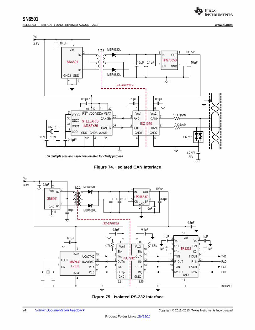
Figure 74. Isolated CAN Interface
Figure 75. Isolated RS-232 Interface
24 Submit Documentation Feedback Copyright © 2012–2013, Texas Instruments Incorporated
Product Folder Links :SN6501

VCC1 VCC2
GND1 GND2
OUTA
16
14
13
2,8 9,154
XOUT
XIN
5
6
2
MSP430
G2132(14-PW)
INA
OUTD
1
3
4
5
6
ISO7641
DVss
DVcc
0.1µF
0.1µF 0.1µF
EN1 EN27 10
INB12
11
OUTB
OUTC
IND
0.1µF
INC
SDI
P1.4
SCLK
SDO9
6
7
8
4.7k 4.7k
28
VBD
AGND
CH0
1,22
CS
26
23
24
25SCLK
SDI
20
SDO
ADS7953
CH155
BDGND
27
32
VA
31
REFP
2
MXO
3
AINP
REFM
30
VIN
GND
VOUT2 6
4REF50251µF
10µF
VS
0.1µF
MBR0520L
MBR0520L
1:1.5
0.1µF
3
1
D2
SN6501
D1
Vcc
4,5
2
GND
3.3V
IN
EN GND
OUT4 1
23TLV70733
10µF
3.3VISO
10µF22µF
16 Analog
Inputs
ISO-BARRIER
Vcc1 Vcc2
GND1 GND2
OUTA
16
14
13
2,8 9,15
P3.1
P3.0
UCB0CLK
UCB0SOMI12
11
14
13
4
XOUT
XIN
5
6
2
MSP430
F2132
INA
OUTD
1
3
4
5
6
ISO7242
DVss
DVcc
0.1µF
0.1µF 0.1µF
EN1 EN27 10
INB
12
11
OUTB
INC
IND
15
0.1µF
OUTC
10V..34V 0V
HV Supply bus
Vcc
GND
DB1
28
LD
16
26
25
23
SIP DB027
CLK
SOP
RLIM
NC
CE
2
13
1
14
24
IP4
IP3
IP5
IP6
11
18
9
20
22
12
17
19
21
10
HOT
4
6
8
RE0
RE1
IP0
IP1
IP2
3
5
7RE2
RE3
RE4
RE5
RE6
RE7 IP7
SN
65H
VS
885
44.8k
10µF
VIN
0.1µF
MBR0520L
MBR0520L
1:2.2
0.1µF
3
1
D2
SN6501
D1
Vcc
4,5
2
GND
3.3V
1 5
43
3.3µF
10µF
5VISO
IN
ONGND
OUT
LP2985-50
BP
2 10nF
SN6501www.ti.com SLLSEA0F –FEBRUARY 2012–REVISED AUGUST 2013
Figure 76. Isolated Digital Input Module
Figure 77. Isolated SPI Interface for an Analog Input Module with 16 Inputs
Copyright © 2012–2013, Texas Instruments Incorporated Submit Documentation Feedback 25
Product Folder Links :SN6501
Vcc1 Vcc2
GND1 GND2
8
7
4 54
XOUT
XIN
5
6
2
MSP430
G2132
1
2
3ISO7421
DVss
DVcc
0.1µF 0.1µF
6P3.0
P3.1
11
12
10µF
VS
0.1µF
MBR0520L
MBR0520L
1:1.5
0.1µF
3
1
D2
SN6501
D1
Vcc
4,5
2
GND
3.3V
IN
EN GND
OUT1 5
23TPS76333
10µF
10µF
INAOUTA
INB OUTB
0.1µF
15
VA
BASE
10
8
DBACK
DIN
16
DAC161P997
OUT9COMA
1
3
2
C2
13
C1
14
5
4
LOW
ERRLVL
3.3VISO
ISO-BARRIER
0.1µF
0.1µF20 W
VD
COMDC3
12
3 x 2.2nF
0.1µF 1µF
LOOP+
LOOP-
20 W
Vcc1 Vcc2
GND1 GND2
8
7
4 54
XOUT
XIN
5
6
2
MSP430
G2132
1
2
3 ISO1541
DVss
DVcc
0.1µF0.1µF 0.1µF
6SDA
SCL
9
8
10µF
VS
0.1µF
MBR0520L
MBR0520L
1:2.2
0.1µF
3
1
D2
SN6501
D1
Vcc
4,5
2
GND
3.3V
IN
ON GND
OUT1 5
23LP2981-50 10µF
10µF
SDA2SDA1
SCL1 SCL2
1.5k 1.5k 1.5k 1.5k
0.1µF
8
VDD
GND
AIN0
2
1
9
10SDA
SCL
4
ADDR
ADS1115
AIN3RDY
3
4 Analog
Inputs
7
VIN
GND
VOUT26
4REF5040
1µF22µF0.1µF
4
VDD
VOUTA11
10SDA
SCL
1
DAC8574
VOUTD8GND
6
12 3
VREFHA2
15
IOVDD
VREFL
5
4 Analog
Outputs
A3
16
A0
13
9
14LDAC
A1
5VISO
5VISO
5VISO
5VISO
SD
A
SC
LISO-BARRIER
1W
SN6501SLLSEA0F –FEBRUARY 2012–REVISED AUGUST 2013 www.ti.com
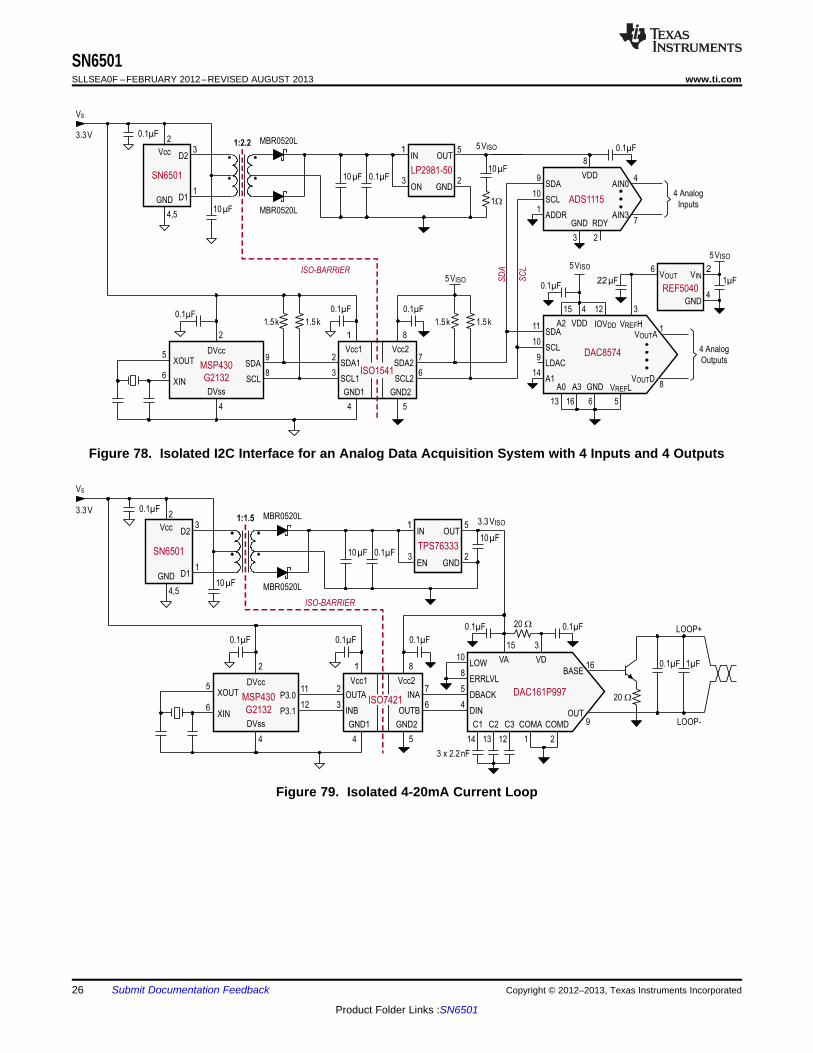
Figure 78. Isolated I2C Interface for an Analog Data Acquisition System with 4 Inputs and 4 Outputs
Figure 79. Isolated 4-20mA Current Loop
26 Submit Documentation Feedback Copyright © 2012–2013, Texas Instruments Incorporated
Product Folder Links :SN6501

SN6501www.ti.com SLLSEA0F –FEBRUARY 2012–REVISED AUGUST 2013
REVISION HISTORY
Changes from Original (February 2012) to Revision A Page
• Changed the device From: Product Preview To: Production ................................................................................................ 1• Added Figure 31 through Figure 34 ...................................................................................................................................... 9• Changed Equation 8 ........................................................................................................................................................... 20• Changed Equation 9 ........................................................................................................................................................... 20• Changed Table 4, From: Wuerth-Elektronik / Midcom To: Wurth Electronics Midcom Inc ................................................ 22• Changed Figure 77 ............................................................................................................................................................. 25
Changes from Revision A (March 2012) to Revision B Page
• Changed Feature From: Small 5-pin DBV Package To: Small 5-pin SOT23 Package ........................................................ 1• Changed Figure 68 title ...................................................................................................................................................... 20
Changes from Revision B (March 2012) to Revision C Page
• Changed the fOSC Oscillator frequency values ...................................................................................................................... 4• Changed Equation 2 ........................................................................................................................................................... 19
Changes from Revision C (March 2012) to Revision D Page
• Changed fOSC, Oscillator frequency To: fSW, D1, D2 Switching frequency ........................................................................... 4• Added graphs Figure 3 through Figure 8 .............................................................................................................................. 5• Added Figure 51 through Figure 54 .................................................................................................................................... 12• Changed the title of Figure 56 From: D1, D2 Oscillator Frequency vs Free-Air Temperature To: D1, D2 Switching
Frequency vs Free-Air Temperature ................................................................................................................................... 13• Added section: Recommended Transformers .................................................................................................................... 20• Changed the location and title of Figure 68 ........................................................................................................................ 20
Changes from Revision D (September 2012) to Revision E Page
• Changed Figure 22 ............................................................................................................................................................... 7
Changes from Revision E (January 2013) to Revision F Page
• Added Figure 9 through Figure 14 ........................................................................................................................................ 5• Added Figure 19 and Figure 20 ............................................................................................................................................ 7• Added Figure 23 through Figure 30 ...................................................................................................................................... 8• Changed Table 2 - Recommended Isolation Transformers Optimized for SN6501 ........................................................... 21
Copyright © 2012–2013, Texas Instruments Incorporated Submit Documentation Feedback 27
Product Folder Links :SN6501

PACKAGE OPTION ADDENDUM
www.ti.com 5-Aug-2013
Addendum-Page 1
PACKAGING INFORMATION
Orderable Device Status(1)
Package Type PackageDrawing
Pins PackageQty
Eco Plan(2)
Lead/Ball Finish MSL Peak Temp(3)
Op Temp (°C) Device Marking(4/5)
Samples
SN6501DBVR ACTIVE SOT-23 DBV 5 3000 Green (RoHS& no Sb/Br)
CU NIPDAU Level-1-260C-UNLIM -40 to 125 6501
SN6501DBVT ACTIVE SOT-23 DBV 5 250 Green (RoHS& no Sb/Br)
CU NIPDAU Level-1-260C-UNLIM -40 to 125 6501
(1) The marketing status values are defined as follows:ACTIVE: Product device recommended for new designs.LIFEBUY: TI has announced that the device will be discontinued, and a lifetime-buy period is in effect.NRND: Not recommended for new designs. Device is in production to support existing customers, but TI does not recommend using this part in a new design.PREVIEW: Device has been announced but is not in production. Samples may or may not be available.OBSOLETE: TI has discontinued the production of the device.
(2) Eco Plan - The planned eco-friendly classification: Pb-Free (RoHS), Pb-Free (RoHS Exempt), or Green (RoHS & no Sb/Br) - please check http://www.ti.com/productcontent for the latest availabilityinformation and additional product content details.TBD: The Pb-Free/Green conversion plan has not been defined.Pb-Free (RoHS): TI's terms "Lead-Free" or "Pb-Free" mean semiconductor products that are compatible with the current RoHS requirements for all 6 substances, including the requirement thatlead not exceed 0.1% by weight in homogeneous materials. Where designed to be soldered at high temperatures, TI Pb-Free products are suitable for use in specified lead-free processes.Pb-Free (RoHS Exempt): This component has a RoHS exemption for either 1) lead-based flip-chip solder bumps used between the die and package, or 2) lead-based die adhesive used betweenthe die and leadframe. The component is otherwise considered Pb-Free (RoHS compatible) as defined above.Green (RoHS & no Sb/Br): TI defines "Green" to mean Pb-Free (RoHS compatible), and free of Bromine (Br) and Antimony (Sb) based flame retardants (Br or Sb do not exceed 0.1% by weightin homogeneous material)
(3) MSL, Peak Temp. -- The Moisture Sensitivity Level rating according to the JEDEC industry standard classifications, and peak solder temperature.
(4) There may be additional marking, which relates to the logo, the lot trace code information, or the environmental category on the device.
(5) Multiple Device Markings will be inside parentheses. Only one Device Marking contained in parentheses and separated by a "~" will appear on a device. If a line is indented then it is a continuationof the previous line and the two combined represent the entire Device Marking for that device.
Important Information and Disclaimer:The information provided on this page represents TI's knowledge and belief as of the date that it is provided. TI bases its knowledge and belief on informationprovided by third parties, and makes no representation or warranty as to the accuracy of such information. Efforts are underway to better integrate information from third parties. TI has taken andcontinues to take reasonable steps to provide representative and accurate information but may not have conducted destructive testing or chemical analysis on incoming materials and chemicals.TI and TI suppliers consider certain information to be proprietary, and thus CAS numbers and other limited information may not be available for release.
In no event shall TI's liability arising out of such information exceed the total purchase price of the TI part(s) at issue in this document sold by TI to Customer on an annual basis.
PACKAGE OPTION ADDENDUM
www.ti.com 5-Aug-2013
Addendum-Page 2
OTHER QUALIFIED VERSIONS OF SN6501 :
• Automotive: SN6501-Q1
NOTE: Qualified Version Definitions:
• Automotive - Q100 devices qualified for high-reliability automotive applications targeting zero defects
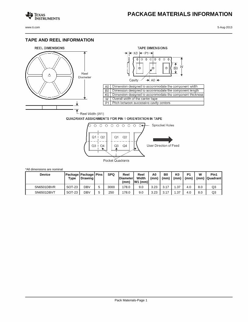
TAPE AND REEL INFORMATION
*All dimensions are nominal
Device PackageType
PackageDrawing
Pins SPQ ReelDiameter
(mm)
ReelWidth
W1 (mm)
A0(mm)
B0(mm)
K0(mm)
P1(mm)
W(mm)
Pin1Quadrant
SN6501DBVR SOT-23 DBV 5 3000 178.0 9.0 3.23 3.17 1.37 4.0 8.0 Q3
SN6501DBVT SOT-23 DBV 5 250 178.0 9.0 3.23 3.17 1.37 4.0 8.0 Q3
PACKAGE MATERIALS INFORMATION
www.ti.com 5-Aug-2013
Pack Materials-Page 1

*All dimensions are nominal
Device Package Type Package Drawing Pins SPQ Length (mm) Width (mm) Height (mm)
SN6501DBVR SOT-23 DBV 5 3000 180.0 180.0 18.0
SN6501DBVT SOT-23 DBV 5 250 180.0 180.0 18.0
PACKAGE MATERIALS INFORMATION
www.ti.com 5-Aug-2013
Pack Materials-Page 2


IMPORTANT NOTICE
Texas Instruments Incorporated and its subsidiaries (TI) reserve the right to make corrections, enhancements, improvements and otherchanges to its semiconductor products and services per JESD46, latest issue, and to discontinue any product or service per JESD48, latestissue. Buyers should obtain the latest relevant information before placing orders and should verify that such information is current andcomplete. All semiconductor products (also referred to herein as “components”) are sold subject to TI’s terms and conditions of salesupplied at the time of order acknowledgment.
TI warrants performance of its components to the specifications applicable at the time of sale, in accordance with the warranty in TI’s termsand conditions of sale of semiconductor products. Testing and other quality control techniques are used to the extent TI deems necessaryto support this warranty. Except where mandated by applicable law, testing of all parameters of each component is not necessarilyperformed.
TI assumes no liability for applications assistance or the design of Buyers’ products. Buyers are responsible for their products andapplications using TI components. To minimize the risks associated with Buyers’ products and applications, Buyers should provideadequate design and operating safeguards.
TI does not warrant or represent that any license, either express or implied, is granted under any patent right, copyright, mask work right, orother intellectual property right relating to any combination, machine, or process in which TI components or services are used. Informationpublished by TI regarding third-party products or services does not constitute a license to use such products or services or a warranty orendorsement thereof. Use of such information may require a license from a third party under the patents or other intellectual property of thethird party, or a license from TI under the patents or other intellectual property of TI.
Reproduction of significant portions of TI information in TI data books or data sheets is permissible only if reproduction is without alterationand is accompanied by all associated warranties, conditions, limitations, and notices. TI is not responsible or liable for such altereddocumentation. Information of third parties may be subject to additional restrictions.
Resale of TI components or services with statements different from or beyond the parameters stated by TI for that component or servicevoids all express and any implied warranties for the associated TI component or service and is an unfair and deceptive business practice.TI is not responsible or liable for any such statements.
Buyer acknowledges and agrees that it is solely responsible for compliance with all legal, regulatory and safety-related requirementsconcerning its products, and any use of TI components in its applications, notwithstanding any applications-related information or supportthat may be provided by TI. Buyer represents and agrees that it has all the necessary expertise to create and implement safeguards whichanticipate dangerous consequences of failures, monitor failures and their consequences, lessen the likelihood of failures that might causeharm and take appropriate remedial actions. Buyer will fully indemnify TI and its representatives against any damages arising out of the useof any TI components in safety-critical applications.
In some cases, TI components may be promoted specifically to facilitate safety-related applications. With such components, TI’s goal is tohelp enable customers to design and create their own end-product solutions that meet applicable functional safety standards andrequirements. Nonetheless, such components are subject to these terms.
No TI components are authorized for use in FDA Class III (or similar life-critical medical equipment) unless authorized officers of the partieshave executed a special agreement specifically governing such use.
Only those TI components which TI has specifically designated as military grade or “enhanced plastic” are designed and intended for use inmilitary/aerospace applications or environments. Buyer acknowledges and agrees that any military or aerospace use of TI componentswhich have not been so designated is solely at the Buyer's risk, and that Buyer is solely responsible for compliance with all legal andregulatory requirements in connection with such use.
TI has specifically designated certain components as meeting ISO/TS16949 requirements, mainly for automotive use. In any case of use ofnon-designated products, TI will not be responsible for any failure to meet ISO/TS16949.
Products Applications
Audio www.ti.com/audio Automotive and Transportation www.ti.com/automotive
Amplifiers amplifier.ti.com Communications and Telecom www.ti.com/communications
Data Converters dataconverter.ti.com Computers and Peripherals www.ti.com/computers
DLP® Products www.dlp.com Consumer Electronics www.ti.com/consumer-apps
DSP dsp.ti.com Energy and Lighting www.ti.com/energy
Clocks and Timers www.ti.com/clocks Industrial www.ti.com/industrial
Interface interface.ti.com Medical www.ti.com/medical
Logic logic.ti.com Security www.ti.com/security
Power Mgmt power.ti.com Space, Avionics and Defense www.ti.com/space-avionics-defense
Microcontrollers microcontroller.ti.com Video and Imaging www.ti.com/video
RFID www.ti-rfid.com
OMAP Applications Processors www.ti.com/omap TI E2E Community e2e.ti.com
Wireless Connectivity www.ti.com/wirelessconnectivity
Mailing Address: Texas Instruments, Post Office Box 655303, Dallas, Texas 75265Copyright © 2013, Texas Instruments Incorporated