Embed Size (px)
Citation preview
www.ti.com
FEATURES
APPLICATIONS
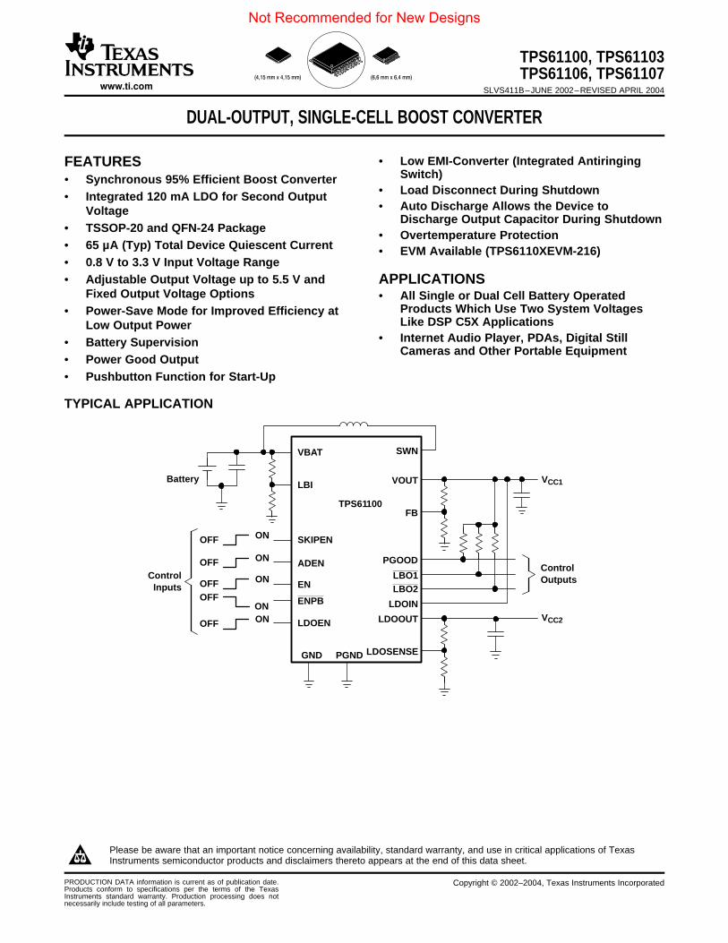
TYPICAL APPLICATION
OFF ON
OFF ON
OFF ON
OFFON
OFF ON
VBAT
LBI
SKIPEN
ADEN
EN
ENPB
LDOEN
SWN
VOUT
FB
PGOOD
LBO1LBO2
LDOIN
LDOOUT
LDOSENSEGND PGND
ControlInputs
ControlOutputs
VCC1
VCC2
TPS61100
Battery
TPS61100, TPS61103TPS61106, TPS61107
SLVS411B–JUNE 2002–REVISED APRIL 2004
DUAL-OUTPUT, SINGLE-CELL BOOST CONVERTER
• Low EMI-Converter (Integrated AntiringingSwitch)• Synchronous 95% Efficient Boost Converter
• Load Disconnect During Shutdown• Integrated 120 mA LDO for Second Output• Auto Discharge Allows the Device toVoltage
Discharge Output Capacitor During Shutdown• TSSOP-20 and QFN-24 Package • Overtemperature Protection• 65 µA (Typ) Total Device Quiescent Current • EVM Available (TPS6110XEVM-216)• 0.8 V to 3.3 V Input Voltage Range• Adjustable Output Voltage up to 5.5 V and
Fixed Output Voltage Options • All Single or Dual Cell Battery OperatedProducts Which Use Two System Voltages• Power-Save Mode for Improved Efficiency atLike DSP C5X ApplicationsLow Output Power
• Internet Audio Player, PDAs, Digital Still• Battery SupervisionCameras and Other Portable Equipment
• Power Good Output• Pushbutton Function for Start-Up
Please be aware that an important notice concerning availability, standard warranty, and use in critical applications of TexasInstruments semiconductor products and disclaimers thereto appears at the end of this data sheet.
PRODUCTION DATA information is current as of publication date. Copyright © 2002–2004, Texas Instruments IncorporatedProducts conform to specifications per the terms of the TexasInstruments standard warranty. Production processing does notnecessarily include testing of all parameters.
Not Recommended for New Designs
www.ti.com
DESCRIPTION
TPS61100, TPS61103TPS61106, TPS61107SLVS411B–JUNE 2002–REVISED APRIL 2004
These devices have limited built-in ESD protection. The leads should be shorted together or the deviceplaced in conductive foam during storage or handling to prevent electrostatic damage to the MOS gates.
The TPS6110x devices provide a complete power supply solution for products powered by either one or twoAlkaline, NiCd, or NiMH battery cells. The converter generates two stable output voltages that are either adjustedby an external resistor divider or fixed internally on the chip. It stays in operation with supply voltages down to0.8 V. The implemented boost converter is based on a fixed frequency, pulse-width-modulation (PWM) controllerusing a synchronous rectifier to obtain maximum efficiency.
The maximum peak current in the boost switch is limited to a value of 1800 mA.
The converter can be disabled to minimize battery drain. During shutdown, the load is completely disconnectedfrom the battery. An auto discharge function allows discharging the output capacitors during shutdown mode.This is especially useful in microcontroller applications where the microcontroller or microprocessor should notremain active due to the stored voltage on the output capacitors. Programming the ADEN-pin disables thisfeature. A low-EMI mode is implemented to reduce ringing and in effect lower radiated electromagnetic energywhen the converter enters the discontinuous conduction mode. A power good output at the boost stage providesadditional control of cascaded power supply components.
The built-in LDO can be used for a second output voltage derived either from the boost output or directly fromthe battery. The output voltage of this LDO can be programmed by an external resistor divider or is fixedinternally on the chip. The LDO can be enabled separately i.e., using the power good of the boost stage.
The device is packaged in a 20-pin TSSOP (20 PW) package or in a 24-pin QFN (24 RGE) package.
AVAILABLE PACKAGE OPTIONS
PACKAGE CODE
20-Pin TSSOP PW
24-Pin QFN RGE
AVAILABLE OUTPUT VOLTAGE OPTIONS
OUTPUT OUTPUTTA VOLTAGE VOLTAGE PART NUMBER (1) PART NUMBER (1)
DC/DC LDO
Adjustable Adjustable TPS61100PW TPS61100RGE
3.3 V Adjustable TPS61103PW TPS61103RGE40°C to 85°C
3.3 V 1.5 V TPS61106PW TPS61106RGE
3.3 V 1.8 V TPS61107PW TPS61107RGE
(1) The PW package is available taped and reeled. Add R suffix to device type (e.g., TPS61100PWR) toorder quantities of 2000 devices per reel. The RGE package is only available in reels. Add R suffix todevice type (e.g. TPS61100RGER) to order quantities of 3000 devices per reel.
2
Not Recommended for New Designs

www.ti.com
Anti-Ringing
GateCONTROL
PGND
RegulatorError
Amplifier
AutoDischarge
PGND
Control Logic
Vref
Oscillator
TemperatureControl
Low DropoutRegulator
AutoDischarge
GND
Low BatteryComparator
VOUT
PGND
FB
LDOIN
LDOOUT
LDOSENSE
SWN
VBAT
ENENPB
PGOODLDOENSKIPEN
ADEN
GND
LBI
LBO1
LBO2
TPS61100, TPS61103TPS61106, TPS61107
SLVS411B–JUNE 2002–REVISED APRIL 2004
FUNCTIONAL BLOCK DIAGRAM
3
Not Recommended for New Designs
www.ti.com
123
4 56789
10
201918
171615141312
11
VBATLBI
ENPBEN
ADENLDOSENSE
LDOENLDOIN
LDOOUTGND
FBVOUTSKIPENNCSWNPGOODSWNLBO2LBO1PGND
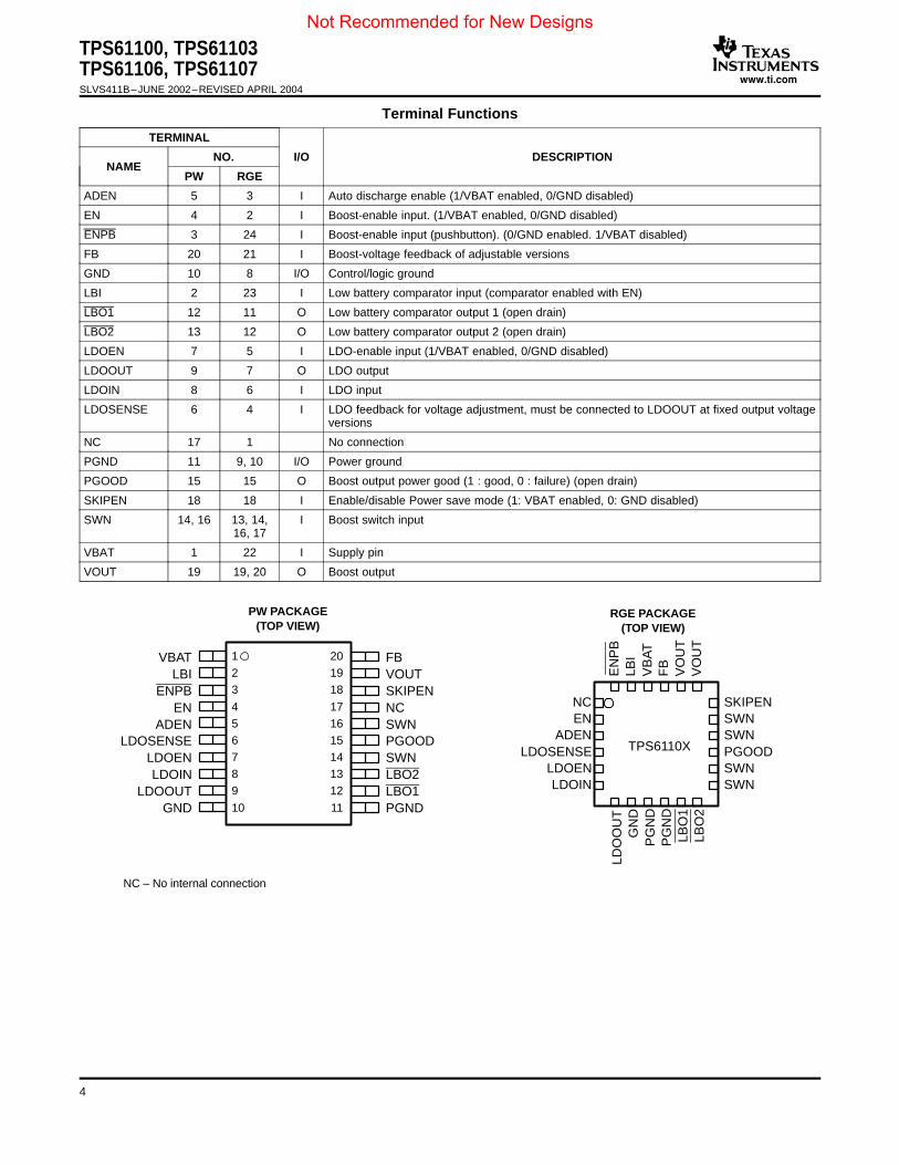
PW PACKAGE(TOP VIEW)
VB
AT
LBI
EN
PB
ENADEN
LDOINLDOEN
LDOSENSE
LBO
2
SWN
PGOODSWN
SKIPENV
OU
T
FB
TPS6110X
LDO
OU
TG
ND
LBO
1
PG
ND
NC
PG
ND
SWNSWN
VO
UT
RGE PACKAGE(TOP VIEW)
NC – No internal connection
TPS61100, TPS61103TPS61106, TPS61107SLVS411B–JUNE 2002–REVISED APRIL 2004
Terminal Functions
TERMINAL
NO. I/O DESCRIPTIONNAME
PW RGE
ADEN 5 3 I Auto discharge enable (1/VBAT enabled, 0/GND disabled)
EN 4 2 I Boost-enable input. (1/VBAT enabled, 0/GND disabled)
ENPB 3 24 I Boost-enable input (pushbutton). (0/GND enabled. 1/VBAT disabled)
FB 20 21 I Boost-voltage feedback of adjustable versions
GND 10 8 I/O Control/logic ground
LBI 2 23 I Low battery comparator input (comparator enabled with EN)
LBO1 12 11 O Low battery comparator output 1 (open drain)
LBO2 13 12 O Low battery comparator output 2 (open drain)
LDOEN 7 5 I LDO-enable input (1/VBAT enabled, 0/GND disabled)
LDOOUT 9 7 O LDO output
LDOIN 8 6 I LDO input
LDOSENSE 6 4 I LDO feedback for voltage adjustment, must be connected to LDOOUT at fixed output voltageversions
NC 17 1 No connection
PGND 11 9, 10 I/O Power ground
PGOOD 15 15 O Boost output power good (1 : good, 0 : failure) (open drain)
SKIPEN 18 18 I Enable/disable Power save mode (1: VBAT enabled, 0: GND disabled)
SWN 14, 16 13, 14, I Boost switch input16, 17
VBAT 1 22 I Supply pin
VOUT 19 19, 20 O Boost output
4
Not Recommended for New Designs
www.ti.com
DETAILED DESCRIPTION
SYNCHRONOUS RECTIFIER
CONTROLLER CIRCUIT
DEVICE ENABLE
LDO ENABLE
POWER GOOD
TPS61100, TPS61103TPS61106, TPS61107
SLVS411B–JUNE 2002–REVISED APRIL 2004
The device integrates an N-channel and a P-channel MOSFET transistor to realize a synchronous rectifier.Because the commonly used discrete Schottky rectifier is replaced with a low RDS(ON) PMOS switch, the powerconversion efficiency reaches 95%. To avoid ground shift due to the high currents in the NMOS switch, twoseparate ground pins are used. The reference for all control functions is the GND pin. The source of the NMOSswitch is connected to PGND. Both grounds must be connected on the PCB at only one point close to the GNDpin. A special circuit is applied to disconnect the load from the input during shutdown of the converter. Inconventional synchronous rectifier circuits, the backgate diode of the high-side PMOS is forward biased inshutdown and allows current flowing from the battery to the output. This device however uses a special circuitwhich takes the cathode of the backgate diode of the high-side PMOS and disconnects it from the source whenthe regulator is not enabled (EN = low).
The benefit of this feature for the system design engineer is that the battery is not depleted during shutdown ofthe converter. No additional components have to be added to the design to make sure that the battery isdisconnected from the output of the converter.
The controller circuit of the device is based on a fixed frequency multiple feedforward controller topology. Inputvoltage, output voltage, and voltage drop on the NMOS switch are monitored and forwarded to the regulator. Sochanges in the operating conditions of the converter directly affect the duty cycle and must not take the indirectand slow way through the control loop and the error amplifier. The control loop, determined by the error amplifier,only has to handle small signal errors. The input for it is the feedback voltage on the FB pin or, at fixed outputvoltage versions, the voltage on the internal resistor divider. It is compared with the internal reference voltage togenerate an accurate and stable output voltage.
The peak current of the NMOS switch is also sensed to limit the maximum current flowing through the switch andthe inductor. The nominal peak current limit is set to 1500 mA.
An internal temperature sensor prevents the device from getting overheated in case of excessive powerdissipation.
The device is put into operation when EN is set high. It is put into a shutdown mode when EN is set to GND. Italso can be enabled with a low signal on ENPB. This forces the converter to start up as long as the low signal isapplied. During this time EN must be set high to prevent the converter from going down into shutdown modeagain. If EN is high, a negative signal on ENPB is ignored.
In shutdown mode, the regulator stops switching, all internal control circuitry including the low-battery comparatoris switched off, and the load is isolated from the input (as described in the synchronous rectifier section). Thisalso means that the output voltage can drop below the input voltage during shutdown. During start-up of theconverter, the duty cycle and the peak current are limited in order to avoid high peak currents drawn from thebattery.
An undervoltage lockout function prevents device start-up if the supply voltage on VBAT is lower thanapproximately 0.7 V. When in operation and the battery is being discharged, the device automatically enters theshutdown mode if the voltage on VBAT drops below approximately 0.7 V. This undervoltage lockout function isimplemented in order to prevent the malfunctioning of the converter.
When the voltage is applied at VBAT, the LDO can be separately enabled and disabled by using the LDOEN pinin the same way as the EN pin at the dc/dc converter stage described above.
The PGOOD pin stays high impedance when the dc/dc converter delivers an output voltage within a definedvoltage window. So it can be used to enable the converter after pushbutton start-up, or to enable any connectedcircuitry such as cascaded converters (LDO) or processor circuits.
5
Not Recommended for New Designs
www.ti.com
POWER SAVE MODE
AUTO DISCHARGE
LOW BATTERY DETECTOR CIRCUIT—LBI/LBO
LOW-EMI SWITCH
LDO
TPS61100, TPS61103TPS61106, TPS61107SLVS411B–JUNE 2002–REVISED APRIL 2004
DETAILED DESCRIPTION (continued)
The SKIPEN pin can be used to select different operation modes. To enable power save, SKIPEN must be sethigh. Power save mode is used to improve efficiency at light load. In power save mode the converter onlyoperates when the output voltage trips below a set threshold voltage. It ramps up the output voltage with one orseveral pulses and goes again into power save mode once the output voltage exceeds the set threshold voltage.This power save mode can be disabled by setting the SKIPEN to GND.
The auto discharge function is needed in applications where the supply voltage of a microcontroller,microprocessor or memory has to be removed during shutdown in order to make sure that the system quicklygoes in a defined state. The auto discharge function is enabled when the ADEN is set high. It is disabled whenthe ADEN is set to GND. When the auto discharge function is enabled, the output capacitor is discharged afterthe device is programmed in the shutdown mode. The output capacitor is discharged by an integrated switch of400 Ω, hence the discharge time depends on the size of the output capacitor.
The low-battery detector circuit is typically used to supervise the battery voltage and to generate an error flagwhen the battery voltage drops below a user-set threshold voltage. The function is active only when the device isenabled. When the device is disabled, both LBO-pin are high-impedance. There are three programmedthresholds, 400 mV, 450 mV, and 500 mV. The outputs on LBO1 and LBO2 are shown as follows:
LBI INPUT LBO1 LBO2(mV)
0-400 0 0
400-450 1 0
450-500 0 1
500-VBAT 1 1
1 means that the output stays at high-impedance and 0 means that the output goes active low. If there is onlyone LBO output needed, both outputs can be tied together. Then the switching threshold is at 500 mV at LBI.
The battery voltage, at which the detection circuit switches, can be programmed with a resistive dividerconnected to the LBI-pin. The resistive divider scales down the battery voltage to a voltage level of 400 mV(450 mV, 500 mV), which is then compared to the LBI threshold voltage. The LBI-pin has a built-in hysteresis of10 mV. See the application section for more details about the programming of the LBI-threshold. If thelow-battery detection circuit is not used, the LBI-pin should be connected to GND (or to VBAT) and the LBO-pincan be left unconnected. Do not let the LBI-pin float.
The device integrates a circuit that removes the ringing that typically appears on the SW-node when theconverter enters discontinuous current mode. In this case, the current through the inductor ramps to zero and therectifying PMOS switch is turned off to prevent a reverse current flowing from the output capacitors back to thebattery. Due to the remaining energy that is stored in parasitic components of the semiconductor and theinductor, a ringing on the SW-pin is induced. The integrated antiringing switch clamps this voltage to VBAT andtherefore dampens ringing.
The built-in LDO can be used to generate a second output voltage derived from the dc/dc converter output, fromthe battery, or from another power source like an ac adapter or a USB power rail. The LDOSENSE input must beconnected to LDOOUT at fixed output voltage versions.
6
Not Recommended for New Designs

www.ti.com
ABSOLUTE MAXIMUM RATINGS (1)
RECOMMENDED OPERATING CONDITIONS
TPS61100, TPS61103TPS61106, TPS61107
SLVS411B–JUNE 2002–REVISED APRIL 2004
over operating free-air temperature range (unless otherwise noted)
UNIT
Input voltage range on VBAT, LBI, SKIPEN, EN, ENPB, ADEN, FB, LDOEN -0.3 V to 3.6 V
Input voltage range on SWN, VOUT, LDOIN, LDOOUT, LDOSENSE, PGOOD, LBO1, LBO2 -0.3 V to 7 V
Operating free air temperature range, TA -40°C to 85°C
Maximum junction temperature, TJ 150°C
Storage temperature range, Tstg -65°C to 150°C
Lead temperature 1,6 mm (1/16 inch) from case for 10s 260°C
(1) Stresses beyond those listed under,, absolute maximum ratings” may cause permanent damage to the device. These are stress ratingsonly, and functional operation of the device at these or any other conditions beyond those indicated under,, recommended operatingconditions” is not implied. Exposure to absolute-maximum-rated conditions for extended periods may affect device reliability.
MIN NOM MAX UNIT
VI Supply voltage at VBAT 0.8 3.3 V
L Boost—inductor 4.7 10 µH
Ci Boost—input capacitor 10 µF
Co Boost—output capacitor 22 100 µF
Ci LDO—input capacitor 1 µF
Co LDO—output capacitor 1 2.2 µF
TJ Operating virtual junction temperature -40 125 °C
7
Not Recommended for New Designs
www.ti.com
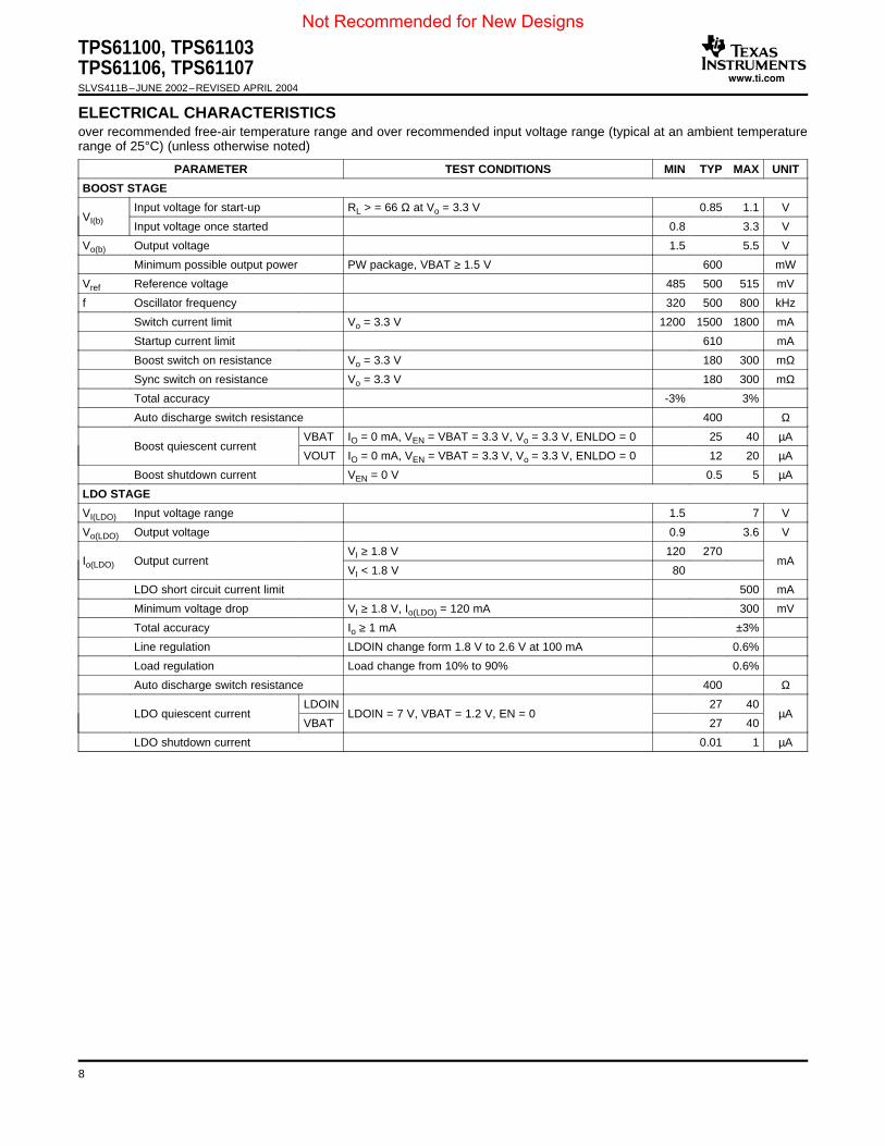
ELECTRICAL CHARACTERISTICS
TPS61100, TPS61103TPS61106, TPS61107SLVS411B–JUNE 2002–REVISED APRIL 2004
over recommended free-air temperature range and over recommended input voltage range (typical at an ambient temperaturerange of 25°C) (unless otherwise noted)
PARAMETER TEST CONDITIONS MIN TYP MAX UNIT
BOOST STAGE
Input voltage for start-up RL > = 66 Ω at Vo = 3.3 V 0.85 1.1 VVI(b) Input voltage once started 0.8 3.3 V
Vo(b) Output voltage 1.5 5.5 V
Minimum possible output power PW package, VBAT ≥ 1.5 V 600 mW
Vref Reference voltage 485 500 515 mV
f Oscillator frequency 320 500 800 kHz
Switch current limit Vo = 3.3 V 1200 1500 1800 mA
Startup current limit 610 mA
Boost switch on resistance Vo = 3.3 V 180 300 mΩ
Sync switch on resistance Vo = 3.3 V 180 300 mΩ
Total accuracy -3% 3%
Auto discharge switch resistance 400 Ω
VBAT IO = 0 mA, VEN = VBAT = 3.3 V, Vo = 3.3 V, ENLDO = 0 25 40 µABoost quiescent current
VOUT IO = 0 mA, VEN = VBAT = 3.3 V, Vo = 3.3 V, ENLDO = 0 12 20 µA
Boost shutdown current VEN = 0 V 0.5 5 µA
LDO STAGE
VI(LDO) Input voltage range 1.5 7 V
Vo(LDO) Output voltage 0.9 3.6 V
VI ≥ 1.8 V 120 270Io(LDO) Output current mA
VI < 1.8 V 80
LDO short circuit current limit 500 mA
Minimum voltage drop VI ≥ 1.8 V, Io(LDO) = 120 mA 300 mV
Total accuracy Io ≥ 1 mA ±3%
Line regulation LDOIN change form 1.8 V to 2.6 V at 100 mA 0.6%
Load regulation Load change from 10% to 90% 0.6%
Auto discharge switch resistance 400 Ω
LDOIN 27 40LDO quiescent current LDOIN = 7 V, VBAT = 1.2 V, EN = 0 µA
VBAT 27 40
LDO shutdown current 0.01 1 µA
8
Not Recommended for New Designs
www.ti.com
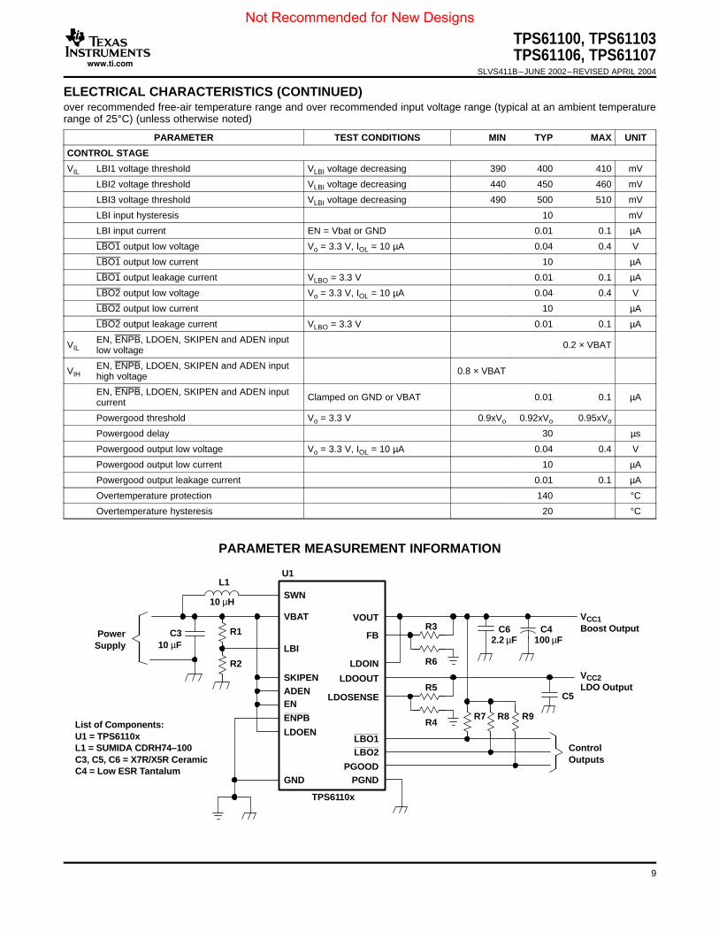
ELECTRICAL CHARACTERISTICS (CONTINUED)
PARAMETER MEASUREMENT INFORMATION
SWN
C310 µF
PowerSupply
L1
10 µH
R1
R2
VBAT VOUT
FBR3
R6LDOIN
R5
R4
LDOSENSE
LDOOUT
R7 R8 R9
C62.2 µF
C4100 µF
U1
LBO1LBO2
PGOODPGND
LBI
SKIPENADENEN
ENPB
LDOEN
GND
TPS6110x
List of Components:U1 = TPS6110xL1 = SUMIDA CDRH74–100C3, C5, C6 = X7R/X5R CeramicC4 = Low ESR Tantalum
VCC1Boost Output
VCC2LDO Output
ControlOutputs
C5
TPS61100, TPS61103TPS61106, TPS61107
SLVS411B–JUNE 2002–REVISED APRIL 2004
over recommended free-air temperature range and over recommended input voltage range (typical at an ambient temperaturerange of 25°C) (unless otherwise noted)
PARAMETER TEST CONDITIONS MIN TYP MAX UNIT
CONTROL STAGE
VIL LBI1 voltage threshold VLBI voltage decreasing 390 400 410 mV
LBI2 voltage threshold VLBI voltage decreasing 440 450 460 mV
LBI3 voltage threshold VLBI voltage decreasing 490 500 510 mV
LBI input hysteresis 10 mV
LBI input current EN = Vbat or GND 0.01 0.1 µA
LBO1 output low voltage Vo = 3.3 V, IOL = 10 µA 0.04 0.4 V
LBO1 output low current 10 µA
LBO1 output leakage current VLBO = 3.3 V 0.01 0.1 µA
LBO2 output low voltage Vo = 3.3 V, IOL = 10 µA 0.04 0.4 V
LBO2 output low current 10 µA
LBO2 output leakage current VLBO = 3.3 V 0.01 0.1 µA
EN, ENPB, LDOEN, SKIPEN and ADEN inputVIL 0.2 × VBATlow voltage
EN, ENPB, LDOEN, SKIPEN and ADEN inputVIH 0.8 × VBAThigh voltage
EN, ENPB, LDOEN, SKIPEN and ADEN input Clamped on GND or VBAT 0.01 0.1 µAcurrent
Powergood threshold Vo = 3.3 V 0.9xVo 0.92xVo 0.95xVo
Powergood delay 30 µs
Powergood output low voltage Vo = 3.3 V, IOL = 10 µA 0.04 0.4 V
Powergood output low current 10 µA
Powergood output leakage current 0.01 0.1 µA
Overtemperature protection 140 °C
Overtemperature hysteresis 20 °C
9
Not Recommended for New Designs
www.ti.com
TYPICAL CHARACTERISTICS
TPS61100, TPS61103TPS61106, TPS61107SLVS411B–JUNE 2002–REVISED APRIL 2004
Table of Graphs
BOOST CONVERTER Figure
vs Input voltage for VOUT = 3.3 V, 5.0 V 1Maximum output current
vs Input voltage for VOUT = 1.8 V, 2.5 V 2
vs Output current for VIN = 1.2 V, VOUT = 1.5 V 3
vs Output current for VIN = 1.2 V, VOUT = 2.5 V 4
vs Output current for VIN = 1.2 V, VOUT = 3.3 V 5
Efficiency vs Output current for VIN = 1.8 V, VOUT = 2.5 V 6
vs Output current for VIN = 2.4 V, VOUT = 3.3 V 7
vs Output current for VIN = 2.4 V, VOUT = 5.0 V 8
vs Input voltage for Iout = 10 mA/100 mA/200 mA, VOUT = 3.3 V 9
Output voltage vs Output current TPS61103/6 10
Minimum start-up supply voltage vs Load resistance 11
No-load supply current into VBAT vs Input voltage 12
No-load supply current into VOUT vs Input voltage 13
Output voltage (ripple) in continuous modeInductor current 14
Output voltage (ripple) in power save modeInductor current 15
Waveforms Load transient response for output current step of 40 mA to 120 mA 16
Line transient response for supply voltage step from 1 V to 1.5 V at Iout = 100 mA 17
Boost converter start-up after enable 18
LDO
vs Input voltage for VOUT = 2.5 V, 3.3 V 19Maximum output current
vs Input voltage for VOUT = 1.5 V, 1.8 V 20
Output voltage vs Output current TPS61106 21
Dropout voltage vs Output current TPS61100 at 3.3 V TPS61106 22
No-load supply current into LDOIN vs Input voltage 23
PSRR vs Frequency 24
Load transient response for output current step of 20 mA to 100 mA 25
Waveforms Line transient response for supply voltage step from 1.8 V to 2.4 V at Iout = 100 mA 26
LDO start-up after enable 27
10
Not Recommended for New Designs

www.ti.com
0
0.2
0.4
0.6
0.8
1
1.2
1.4
VI - Input Voltage - VM
axim
um
Ou
tpu
t Cu
rren
t - A
VO = 1.8 V VO = 2.5 V
0.8 1.81 1.2 1.4 1.6 2 2.2 2.4
TPS61100
0
0.2
0.4
0.6
0.8
1
1.2
0.8 1.8 3VI - Input Voltage - V
VO = 3.3 V
VO = 5 V
1 1.2 1.4 1.6 2 2.2 2.4 2.6 2.8 3.2
TPS61100
Max
imu
m O
utp
ut C
urr
ent -
A
0
10
20
30
40
50
60
70
80
90
100
0.1 1 10 100 1000
Eff
icie
ncy
- %
IO - Output Current - mA
TPS61100VO = 1.5 V,VBAT = 1.2 V
0
10
20
30
40
50
60
70
80
90
100
0.1 1 10 100 1000
Eff
icie
ncy
- %
IO - Output Current - mA
TPS61100VO = 2.5 V,VBAT = 1.2 V
TPS61100, TPS61103TPS61106, TPS61107
SLVS411B–JUNE 2002–REVISED APRIL 2004
MAXIMUM OUTPUT CURRENT MAXIMUM OUTPUT CURRENTvs vs
INPUT VOLTAGE INPUT VOLTAGE
Figure 1. Figure 2.
EFFICIENCY EFFICIENCYvs vs
OUTPUT CURRENT OUTPUT CURRENT
Figure 3. Figure 4.
11
Not Recommended for New Designs
www.ti.com
0
10
20
30
40
50
60
70
80
90
100
0.1 1 10 100 1000
Eff
icie
ncy
- %
IO - Output Current - mA
TPS61106VBAT = 1.2 V
0
10
20
30
40
50
60
70
80
90
100
0.1 1 10 100 1000E
ffic
ien
cy -
%
IO - Output Current - mA
TPS61100VO = 2.5 V,VBAT = 1.8 V
0
10
20
30
40
50
60
70
80
90
100
0.1 1 10 100 1000
Eff
icie
ncy
- %
IO - Output Current - mA
TPS61106VBAT = 2.4 V
0
10
20
30
40
50
60
70
80
90
100
0.1 1 10 100
Eff
icie
ncy
- %
IO - Output Current - mA
TPS61100VO = 5 V,VBAT = 2.4 V
TPS61100, TPS61103TPS61106, TPS61107SLVS411B–JUNE 2002–REVISED APRIL 2004
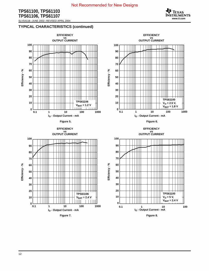
TYPICAL CHARACTERISTICS (continued)
EFFICIENCY EFFICIENCYvs vs
OUTPUT CURRENT OUTPUT CURRENT
Figure 5. Figure 6.
EFFICIENCY EFFICIENCYvs vs
OUTPUT CURRENT OUTPUT CURRENT
Figure 7. Figure 8.
12
Not Recommended for New Designs

www.ti.com
3.18
3.2
3.22
3.24
3.26
3.28
3.3
3.32
3.34
- O
utp
ut
Vo
ltag
e - V
IO - Output Current - mA
VO
TPS61103/6
VBAT = 1.2 V
0.1 1 10 100 10000
10
20
30
40
50
60
70
80
90
100
Eff
icie
ncy
- %
VI - Input Voltage - V
IO = 100 mA
IO = 10 mA
IO = 250 mA
TPS61106
0.8 1 1.2 1.4 1.6 1.8 2 2.2 2.4 2.6 2.8 3 3.2
0.7
0.75
0.8
0.85
0.9
0.95
1
1k10010
Min
imu
m S
tart
up
Su
pp
ly V
olta
ge
- V
Load Resistance - Ω
TPS61106
0
5
10
15
20
25
30
0.8 1 1.2 1.4 1.6 1.8 2 2.2 2.4 2.6 2.8 3 3.2 3.4 3.6
85°C
25°C
-40°C
VI - Input Voltage - V
No
-Lo
ad S
up
ply
Cu
rren
t In
to V
BA
T -
Aµ
TPS61100, TPS61103TPS61106, TPS61107
SLVS411B–JUNE 2002–REVISED APRIL 2004
TYPICAL CHARACTERISTICS (continued)
EFFICIENCY OUTPUT VOLTAGEvs vs
INPUT VOLTAGE OUTPUT CURRENT
Figure 9. Figure 10.
MINIMUM START-UP SUPPLY VOLTAGE NO-LOAD SUPPLY CURRENT INTO VBATvs vs
LOAD RESISTANCE INPUT VOLTAGE
Figure 11. Figure 12.
13
Not Recommended for New Designs
www.ti.com
Inductor Current200 mA/Div, DC
Output Voltage20 mV/Div, AC
Timebase - 1 µs/Div0
2
4
6
8
10
12
14
16
0.8 1 1.2 1.4 1.6 1.8 2 2.2 2.4 2.6 2.8 3 3.2 3.4 3.6
VI - Input Voltage - V
-40°C
85°C
25°C
TPS61106
N0-
Lo
ad S
up
ply
Cu
rren
t In
to -
VO
UT
-
Aµ
Timebase - 500 µs/Div
Inductor Current200 mA/Div, DC
Output Voltage50 mV/Div, AC
Output Voltage20 mV/Div, AC
Output Current50 mA/Div, DC
Timebase - 500 µs/Div
TPS61100, TPS61103TPS61106, TPS61107SLVS411B–JUNE 2002–REVISED APRIL 2004
TYPICAL CHARACTERISTICS (continued)
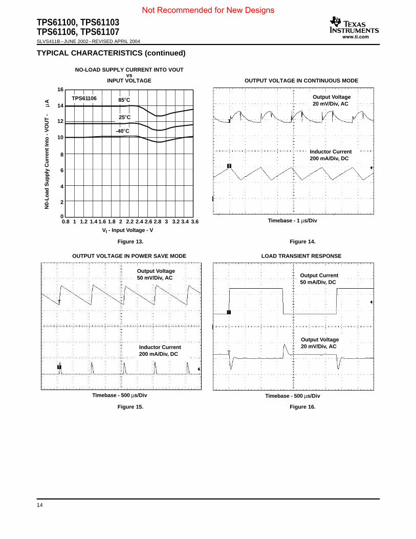
NO-LOAD SUPPLY CURRENT INTO VOUTvs
INPUT VOLTAGE OUTPUT VOLTAGE IN CONTINUOUS MODE
Figure 13. Figure 14.
OUTPUT VOLTAGE IN POWER SAVE MODE LOAD TRANSIENT RESPONSE
Figure 15. Figure 16.
14
Not Recommended for New Designs
www.ti.com
Output Voltage50 mV/Div, AC
Input Voltage500 mV/Div, DC
Timebase - 2 ms/Div
Output Voltage2 V/Div, DC
Input Current500 mA/Div, DC
Enable2 V/Div, DC
Voltage at SW2 V/Div, DC
Timebase - 400 µs/Div
0.1
0.15
0.2
0.25
0.3
0.35
2.5 3 3.5 4 4.5 5 5.5 6 6.5 7
VO = 3.3 V
VO = 2.5 V
Max
imu
m L
DO
Ou
tpu
t Cu
rren
t - A
LDO Input Voltage - V
0.1
0.15
0.2
0.25
0.3
0.35
1.5 2 2.5 3 3.5 4 4.5 5 5.5 6
VO = 1.8 V
VO = 1.5 V
Max
imu
m L
DO
Ou
tpu
t Cu
rren
t - A
LDO Input Voltage - V
TPS61100, TPS61103TPS61106, TPS61107
SLVS411B–JUNE 2002–REVISED APRIL 2004
TYPICAL CHARACTERISTICS (continued)
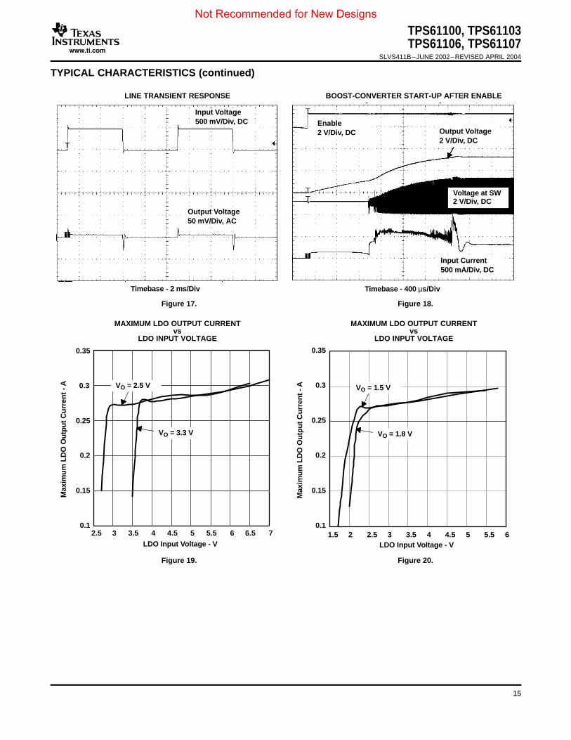
LINE TRANSIENT RESPONSE BOOST-CONVERTER START-UP AFTER ENABLE
Figure 17. Figure 18.
MAXIMUM LDO OUTPUT CURRENT MAXIMUM LDO OUTPUT CURRENTvs vs
LDO INPUT VOLTAGE LDO INPUT VOLTAGE
Figure 19. Figure 20.
15
Not Recommended for New Designs

www.ti.com
1.45
1.46
1.47
1.48
1.49
1.5
1.51
0 50 100 150 200
LD
O O
utp
ut
Vo
ltag
e - V
LDO Output Current - mA
TPS61106LDOIN = 1.8 V
0
0.5
1
1.5
2
2.5
3
3.5
0 100 200 300 400 500
TPS61106(LDO OUTPUT
VOLTAGE 1.5 V)
TPS61100(LDO OUTPUTVOLTAGE 3.3 V)
LD
O D
rop
ou
t V
olta
ge
- V
LDO Output Current - mA
1k 10k 100k 1M 10M0
10
20
30
40
70
60
50
80
PS
RR
- d
B
f - Frequency - Hz
LDO Output Current 10 mA
LDO Output Current 100 mA
TPS61106LDOIN = 3.3 V
0
5
10
15
20
25
30
35
0.8 1 1.2 1.4 1.6 1.8 2 2.2 2.4 2.6 2.8 3 3.2 3.4 3.6
85°C
25°C
-40°C
LDOIN Input Voltage - V
Su
pp
ly C
urr
ent
Into
LD
OIN
-
Aµ
TPS61100, TPS61103TPS61106, TPS61107SLVS411B–JUNE 2002–REVISED APRIL 2004
TYPICAL CHARACTERISTICS (continued)
LDO OUTPUT VOLTAGE LDO DROPOUT VOLTAGEvs vs
LDO OUTPUT CURRENT LDO OUTPUT CURRENT
Figure 21. Figure 22.
SUPPLY CURRENT INTO LDOIN PSRRvs vs
LDOIN INPUT VOLTAGE FREQUENCY
Figure 23. Figure 24.
16
Not Recommended for New Designs

www.ti.com
Output Current50 mA/Div, DC
Output Voltage20 mV/Div, AC
Timebase - 1 ms/Div
Input Voltage1 V/Div, DC
Output Voltage10 mV/Div, AC
Timebase - 2 ms/Div
LDO-Enable2 V/Div, DC
LDO-Output Voltage1 V/Div, DC
Input Current50 mA/Div, DC
Timebase - 50 µs/Div
TPS61100, TPS61103TPS61106, TPS61107
SLVS411B–JUNE 2002–REVISED APRIL 2004
TYPICAL CHARACTERISTICS (continued)
LDO LOAD TRANSIENT RESPONSE LDO LINE TRANSIENT RESPONSE
Figure 25. Figure 26.
LDO START-UP AFTER ENABLE
Figure 27.
17
Not Recommended for New Designs
www.ti.com
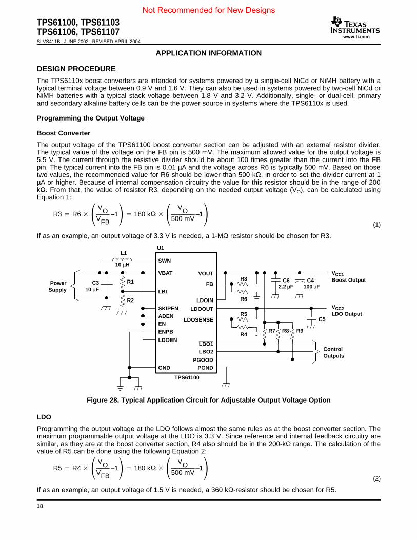
APPLICATION INFORMATION
DESIGN PROCEDURE
Programming the Output Voltage
R3 R6 VOVFB
–1 180 k VO500 mV
–1(1)
SWN
C310 µF
PowerSupply
L1
10 µH
R1
R2
VBAT VOUT
FBR3
R6LDOIN
R5
R4
LDOSENSE
LDOOUT
R7 R8 R9
C62.2 µF
C4100 µF
U1
LBO1LBO2
PGOODPGND
LBI
SKIPENADENEN
ENPB
LDOEN
GND
TPS61100
VCC1Boost Output
VCC2LDO Output
ControlOutputs
C5
R5 R4 VOVFB
–1 180 k VO500 mV
–1(2)
TPS61100, TPS61103TPS61106, TPS61107SLVS411B–JUNE 2002–REVISED APRIL 2004
The TPS6110x boost converters are intended for systems powered by a single-cell NiCd or NiMH battery with atypical terminal voltage between 0.9 V and 1.6 V. They can also be used in systems powered by two-cell NiCd orNiMH batteries with a typical stack voltage between 1.8 V and 3.2 V. Additionally, single- or dual-cell, primaryand secondary alkaline battery cells can be the power source in systems where the TPS6110x is used.
Boost Converter
The output voltage of the TPS61100 boost converter section can be adjusted with an external resistor divider.The typical value of the voltage on the FB pin is 500 mV. The maximum allowed value for the output voltage is5.5 V. The current through the resistive divider should be about 100 times greater than the current into the FBpin. The typical current into the FB pin is 0.01 µA and the voltage across R6 is typically 500 mV. Based on thosetwo values, the recommended value for R6 should be lower than 500 kΩ, in order to set the divider current at 1µA or higher. Because of internal compensation circuitry the value for this resistor should be in the range of 200kΩ. From that, the value of resistor R3, depending on the needed output voltage (VO), can be calculated usingEquation 1:
If as an example, an output voltage of 3.3 V is needed, a 1-MΩ resistor should be chosen for R3.
Figure 28. Typical Application Circuit for Adjustable Output Voltage Option
LDO
Programming the output voltage at the LDO follows almost the same rules as at the boost converter section. Themaximum programmable output voltage at the LDO is 3.3 V. Since reference and internal feedback circuitry aresimilar, as they are at the boost converter section, R4 also should be in the 200-kΩ range. The calculation of thevalue of R5 can be done using the following Equation 2:
If as an example, an output voltage of 1.5 V is needed, a 360 kΩ-resistor should be chosen for R5.
18
Not Recommended for New Designs

www.ti.com
Programming the LBI/LBO Threshold Voltage
R1 R2 VBATVLBI-threshold
–1 390 k VBAT450 mV
–1(3)
VBAT VLBI-threshold R1R2
1 500 mV 680 k390 k
1(4)
Inductor Selection
IL IOUT VOUT
VBAT 0.8(5)
TPS61100, TPS61103TPS61106, TPS61107
SLVS411B–JUNE 2002–REVISED APRIL 2004
APPLICATION INFORMATION (continued)
The current through the resistive divider should be about 100 times greater than the current into the LBI pin. Thetypical current into the LBI pin is 0.01 µA, and the voltage across R2 is equal to the LBI voltage threshold that isgenerated on-chip, which has a value of 400 mV, 450 mV or 500 mV. The recommended value for R2is thereforein the range of 500 kΩ. From that, the value of resistor R1, depending on the desired minimum battery voltageVBAT, can be calculated using Equation 3.
For example, if the low-battery detection circuit should flag an error condition for the 450 mV threshold on theLBO outputs at a battery voltage of 1.23 V, a 680-kΩ resistor should be chosen for R1. The resulting batteryvoltages of the other thresholds can be calculated using Equation 4:
The result for the 500-mV threshold in our example is 1.37 V and for the 400-mV threshold 1.1 V. This results inthe following truth table for the battery supervisor outputs:
VBAT [V] LBO1 LBO2
0-1.1 0 0
1.1-1.23 1 0
1.23-1.37 0 1
1.37-VBAT max 1 1
If the application requires only a simple LBI/LBO function both LBO outputs can be connected together. The LBIthreshold then is 500 mV.
The outputs of the low battery supervisor are simple open-drain outputs that go active low if the dedicated batteryvoltage drops below the programmed threshold voltage on LBI. The output requires a pullup resistor with arecommended value of 1 MΩ. The maximum voltage which is used to pull up the LBO outputs should not exceedthe output voltage of the boost converter. If not used, the LBO pin can be left floating or tied to GND.
A boost converter normally requires two main passive components for storing energy during the conversion. Aboost inductor and a storage capacitor at the output are required. To select the boost inductor, it isrecommended to keep the possible peak inductor current below the current limit threshold of the power switch inthe chosen configuration. For example, the current limit threshold of the TPS6110x's switch is 1200 mA at anoutput voltage of 3.3 V. The highest peak current through the inductor and the switch depends on the outputload, the input (VBAT), and the output voltage (VOUT). Estimation of the maximum average inductor current can bedone using Equation 5:
For example, for an output current of 100 mA at 3.3 V, at least 515 mA of current flows through the inductor at aminimum input voltage of 0.8 V.
19
Not Recommended for New Designs

www.ti.com
L VBAT VOUT–VBAT
IL ƒ VOUT (6)
CAPACITOR SELECTION
Input Capacitor
Output Capacitor Boost Converter
Cmin IOUT VOUT VBAT
ƒ V VOUT (7)
TPS61100, TPS61103TPS61106, TPS61107SLVS411B–JUNE 2002–REVISED APRIL 2004
The second parameter for choosing the inductor is the desired current ripple in the inductor. Normally, it isadvisable to work with a ripple of less than 20% of the average inductor current. A smaller ripple reduces themagnetic hysteresis losses in the inductor, as well as output voltage ripple and EMI. But in the same way,regulation time at load changes rises. In addition, a larger inductor increases the total system costs. With thoseparameters, it is possible to calculate the value for the inductor by using Equation 6:
Parameter 0 is the switching frequency and∆ IL is the ripple current in the inductor, i.e., 20% × IL. In this example,the desired inductor has the value of 12 µH. With this calculated value and the calculated currents, it is possibleto choose a suitable inductor. Care has to be taken that load transients and losses in the circuit can lead tohigher currents as estimated in Equation 5. Also, the losses in the inductor caused by magnetic hysteresis lossesand copper losses are a major parameter for total circuit efficiency.
Table 1. Inductors
VENDOR RECOMMENDED INDUCTOR SERIES
CDRH73
CDRH74Sumida
CDRH5D18
CDRH6D38
DR73Coiltronics
DR74
LQS66CMurata
LQN6C
SLF 7045TDK
SLF 7032
WE-PD Type MWurth Electronic
WE-PD Type S
At least a 10-µF input capacitor is recommended to improve transient behavior of the regulator and EMI behaviorof the total power supply circuit. A ceramic capacitor or a tantalum capacitor with a 100-nF ceramic capacitor inparallel, placed close to the IC, is recommended.
The major parameter necessary to define the output capacitor is the maximum allowed output voltage ripple ofthe converter. This ripple is determined by two parameters of the capacitor, the capacitance and the ESR. It ispossible to calculate the minimum capacitance needed for the defined ripple, supposing that the ESR is zero, byusing Equation 7:
Parameter f is the switching frequency and ∆V is the maximum allowed ripple.
20
Not Recommended for New Designs
www.ti.com
VESR IOUT RESR (8)
Output Capacitor LDO
LAYOUT CONSIDERATIONS
APPLICATION EXAMPLES
SWN
C310 µF
L1
10 µH
R1
R2
VBAT VOUT
LDOIN
LDOSENSE
LDOOUT
R7 R8 R9
C62.2 µF
C4100 µF
U1
LBO1LBO2
PGOODPGND
LBI
SKIPENADENEN
ENPB
LDOEN
GND
TPS61106
List of Components:U1 = TPS61106L1 = SUMIDA CDRH74–100C3, C5, C6 = X7R/X5R CeramicC4 = Low ESR Tantalum
3.3 V,>250 mA
C52.2 µF
1.5 V,>120 mA
LBO1LBO2
PGOOD
TPS61100, TPS61103TPS61106, TPS61107
SLVS411B–JUNE 2002–REVISED APRIL 2004
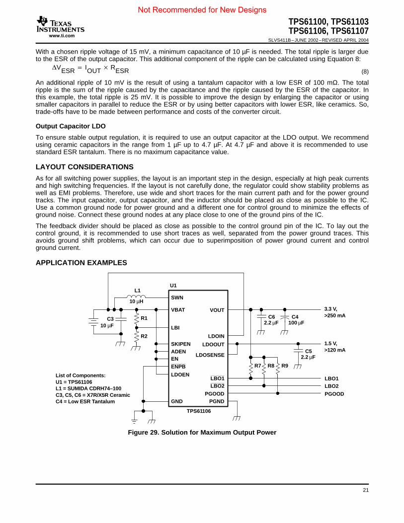
With a chosen ripple voltage of 15 mV, a minimum capacitance of 10 µF is needed. The total ripple is larger dueto the ESR of the output capacitor. This additional component of the ripple can be calculated using Equation 8:
An additional ripple of 10 mV is the result of using a tantalum capacitor with a low ESR of 100 mΩ. The totalripple is the sum of the ripple caused by the capacitance and the ripple caused by the ESR of the capacitor. Inthis example, the total ripple is 25 mV. It is possible to improve the design by enlarging the capacitor or usingsmaller capacitors in parallel to reduce the ESR or by using better capacitors with lower ESR, like ceramics. So,trade-offs have to be made between performance and costs of the converter circuit.
To ensure stable output regulation, it is required to use an output capacitor at the LDO output. We recommendusing ceramic capacitors in the range from 1 µF up to 4.7 µF. At 4.7 µF and above it is recommended to usestandard ESR tantalum. There is no maximum capacitance value.
As for all switching power supplies, the layout is an important step in the design, especially at high peak currentsand high switching frequencies. If the layout is not carefully done, the regulator could show stability problems aswell as EMI problems. Therefore, use wide and short traces for the main current path and for the power groundtracks. The input capacitor, output capacitor, and the inductor should be placed as close as possible to the IC.Use a common ground node for power ground and a different one for control ground to minimize the effects ofground noise. Connect these ground nodes at any place close to one of the ground pins of the IC.
The feedback divider should be placed as close as possible to the control ground pin of the IC. To lay out thecontrol ground, it is recommended to use short traces as well, separated from the power ground traces. Thisavoids ground shift problems, which can occur due to superimposition of power ground current and controlground current.
Figure 29. Solution for Maximum Output Power
21
Not Recommended for New Designs

www.ti.com
SWN
C310 µF
L1
10 µH
R1
R2
VBAT VOUT
LDOIN
LDOSENSE
LDOOUT
R7 R8 R9
C62.2 µF
C4100 µF
U1
LBO1LBO2
PGOODPGND
LBI
SKIPENADENEN
ENPB
LDOEN
GND
TPS61106
List of Components:U1 = TPS61106L1 = SUMIDA 5D18–100C3, C5, C6 = X7R/X5R CeramicC4 = Low ESR, Low Profile Tantalum
3.3 V
C52.2 µF
1.5 V
LBO1LBO2
PGOOD
SWN
C310 µF
L1
10 µH
R1
R2
VBAT VOUT
LDOIN
LDOSENSE
LDOOUT
R7 R8 R9
C62.2 µF
C4100 µF
U1
LBO1LBO2
PGOODPGND
LBI
SKIPENADENEN
ENPB
LDOEN
GND
TPS61106
List of Components:U1 = TPS61106L1 = SUMIDA CDRH74–100C3, C5, C6,C7, C8 = X7R/X5R CeramicC4 = Low ESR TantalumDS1 = BAT54S
3.3 V
C52.2 µF
1.5 V
LBO1LBO2
PGOOD
C7
0.1 µF
DS1
C81 µF
6 V
TPS61100, TPS61103TPS61106, TPS61107SLVS411B–JUNE 2002–REVISED APRIL 2004
Figure 30. Low Profile Solution, Maximum Height 1,8 mm
Figure 31. Dual Power Supply With Auxiliary Positive Output Voltage
22
Not Recommended for New Designs

www.ti.com
SWN
C310 µF
L1
10 µH
R1
R2
VBAT VOUT
LDOIN
LDOSENSE
LDOOUT
R7 R8 R9
C62.2 µF
C4100 µF
U1
LBO1LBO2
PGOODPGND
LBI
SKIPENADENEN
ENPB
LDOEN
GND
TPS61106
List of Components:U1 = TPS61106L1 = SUMIDA CDRH74–100C3, C5, C6,C7, C8 = X7R/X5R CeramicC4 = Low ESR TantalumDS1 = BAT54S
3.3 V
C52.2 µF
1.5 V
LBO1LBO2
PGOOD
C7
0.1 µF
DS1C8
1 µF
–3 V
SWN
C310 µF
L1
10 µH
R1
R2
VBAT VOUT
FBR3
R6LDOIN
R5
R4
LDOSENSE
LDOOUT
R7 R8 R9
C622 µF
C52.2 µF
U1
LBO1LBO2
PGOODPGND
LBI
SKIPENADENEN
ENPB
LDOEN
GND
TPS61100
List of Components:U1 = TPS61100L1 = SUMIDA CDRH74–100C3, C5 = X7R/X5R CeramicC6 = X7R/X5R Ceramic or Low ESR Tantalum
3.3 V
LBO1LBO2
PGOOD
TPS61100, TPS61103TPS61106, TPS61107
SLVS411B–JUNE 2002–REVISED APRIL 2004
Figure 32. Dual Power Supply With Auxiliary Negative Output Voltage
Figure 33. Single Output Using LDO as Filter
23
Not Recommended for New Designs

www.ti.com
SWN
C310 µF
L1
10 µH
R1
R2
VBAT VOUT
LDOIN
LDOSENSE
LDOOUT
R7 R8 R9
C62.2 µF
C4100 µF
U1
LBO1LBO2
PGOODPGND
LBI
SKIPENADENEN
ENPB
LDOEN
GND
TPS61106
List of Components:U1 = TPS61106L1 = SUMIDA 5D18–100C3, C5, C6 = X7R/X5R CeramicC4 = Low ESR Tantalum
3.3 V
C52.2 µF
1.5 V
LBO1LBO2
R10
SWN
C310 µF
USB-Input4.2 V – 5.5 V
L1
10 µH
R1
R2
VBAT VOUT
FBR3 1 MΩ
R6180 kΩ
LDOIN
R5 1.022 MΩ
R4180 kΩ
LDOSENSE
LDOOUT
R7 R8 R9
C62.2 µF
C4100 µF
U1
LBO1LBO2
PGOODPGND
LBI
SYNCADENEN
ENPB
LDOEN
GND
TPS61100
VCC3.3 V SystemSupply
ControlOutputs
R10680 kΩ
R111 MΩ
R12180 kΩ
D2
D1
List of Components:U1 = TPS61100L1 = SUMIDA CDRH73–100C3, C6 = X7R/X5R CeramicC4 = Low ESR TantalumD1 = ON-Semiconductor MBR0520
TPS61100, TPS61103TPS61106, TPS61107SLVS411B–JUNE 2002–REVISED APRIL 2004
Figure 34. Simple Solution Using a Pushbutton for Start-Up
Figure 35. Dual Input Power Supply
24
Not Recommended for New Designs

www.ti.com
SWN
C310 µF
L1
10 µH
R1
R2
VBAT VOUT
FB
LDOIN
LDOSENSE
LDOOUT
R7 R8 R9
C62.2 µF
C4100 µF
U1
LBO1LBO2
PGOODPGND
LBI
SKIPENADEN
EN
ENPB
LDOEN
GND
TPS6110XRGE
C52.2 µF
R3
R6
R5
R4
LBO1LBO2PGOOD
LDOOUT
OUTPUT
LDOEN
ENPB
EN
ADEN
SKIPEN
INPUT
R11
R10
THERMAL INFORMATION
PD(MAX) TJ(MAX) TA
RJA
150°C 85°C155 kW
420 mW(9)
TPS61100, TPS61103TPS61106, TPS61107
SLVS411B–JUNE 2002–REVISED APRIL 2004
Figure 36. TPS6110x EVM Circuit Diagram
Implementation of integrated circuits in low-profile and fine-pitch surface-mount packages typically requiresspecial attention to power dissipation. Many system-dependent issues such as thermal coupling, airflow, addedheat sinks and convection surfaces, and the presence of other heat-generating components affect thepower-dissipation limits of a given component.
Three basic approaches for enhancing thermal performance are listed below.• Improving the power dissipation capability of the PCB design.• Improving the thermal coupling of the component to the PCB.• Introducing airflow in the system.
The maximum junction temperature (TJ) of the TPS6110x devices is 150°C. The thermal resistance of the 20-pinTSSOP package (PW) isRΘJA = 155 K/W (QFN package, RGE, 161 K/W). Specified regulator operation isassured to a maximum ambient temperature TA of 85°C. Therefore, the maximum power dissipation is about 420mW. More power can be dissipated if the maximum ambient temperature of the application is lower.
25
Not Recommended for New Designs
PACKAGE OPTION ADDENDUM
www.ti.com 10-Jun-2014
Addendum-Page 1
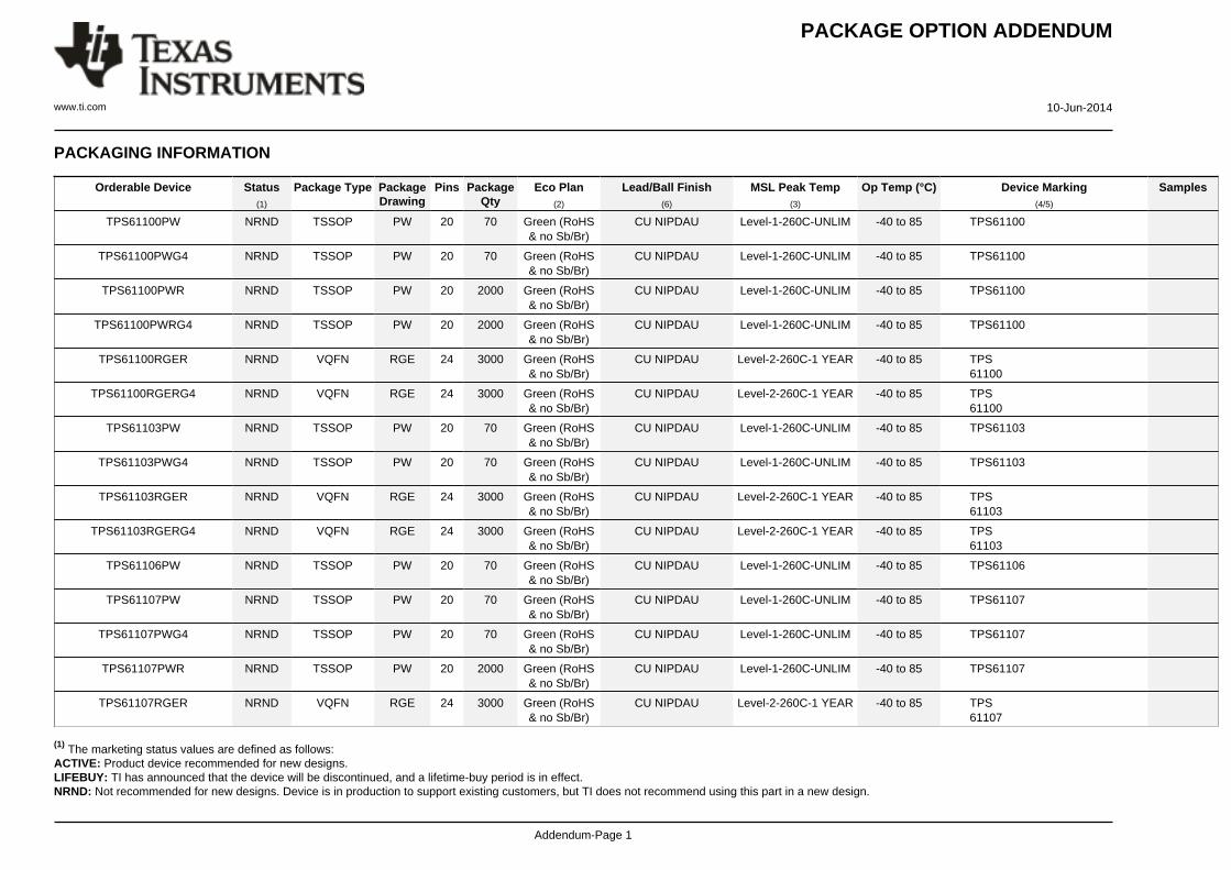
PACKAGING INFORMATION
Orderable Device Status(1)
Package Type PackageDrawing
Pins PackageQty
Eco Plan(2)
Lead/Ball Finish(6)
MSL Peak Temp(3)
Op Temp (°C) Device Marking(4/5)
Samples
TPS61100PW NRND TSSOP PW 20 70 Green (RoHS& no Sb/Br)
CU NIPDAU Level-1-260C-UNLIM -40 to 85 TPS61100
TPS61100PWG4 NRND TSSOP PW 20 70 Green (RoHS& no Sb/Br)
CU NIPDAU Level-1-260C-UNLIM -40 to 85 TPS61100
TPS61100PWR NRND TSSOP PW 20 2000 Green (RoHS& no Sb/Br)
CU NIPDAU Level-1-260C-UNLIM -40 to 85 TPS61100
TPS61100PWRG4 NRND TSSOP PW 20 2000 Green (RoHS& no Sb/Br)
CU NIPDAU Level-1-260C-UNLIM -40 to 85 TPS61100
TPS61100RGER NRND VQFN RGE 24 3000 Green (RoHS& no Sb/Br)
CU NIPDAU Level-2-260C-1 YEAR -40 to 85 TPS61100
TPS61100RGERG4 NRND VQFN RGE 24 3000 Green (RoHS& no Sb/Br)
CU NIPDAU Level-2-260C-1 YEAR -40 to 85 TPS61100
TPS61103PW NRND TSSOP PW 20 70 Green (RoHS& no Sb/Br)
CU NIPDAU Level-1-260C-UNLIM -40 to 85 TPS61103
TPS61103PWG4 NRND TSSOP PW 20 70 Green (RoHS& no Sb/Br)
CU NIPDAU Level-1-260C-UNLIM -40 to 85 TPS61103
TPS61103RGER NRND VQFN RGE 24 3000 Green (RoHS& no Sb/Br)
CU NIPDAU Level-2-260C-1 YEAR -40 to 85 TPS61103
TPS61103RGERG4 NRND VQFN RGE 24 3000 Green (RoHS& no Sb/Br)
CU NIPDAU Level-2-260C-1 YEAR -40 to 85 TPS61103
TPS61106PW NRND TSSOP PW 20 70 Green (RoHS& no Sb/Br)
CU NIPDAU Level-1-260C-UNLIM -40 to 85 TPS61106
TPS61107PW NRND TSSOP PW 20 70 Green (RoHS& no Sb/Br)
CU NIPDAU Level-1-260C-UNLIM -40 to 85 TPS61107
TPS61107PWG4 NRND TSSOP PW 20 70 Green (RoHS& no Sb/Br)
CU NIPDAU Level-1-260C-UNLIM -40 to 85 TPS61107
TPS61107PWR NRND TSSOP PW 20 2000 Green (RoHS& no Sb/Br)
CU NIPDAU Level-1-260C-UNLIM -40 to 85 TPS61107
TPS61107RGER NRND VQFN RGE 24 3000 Green (RoHS& no Sb/Br)
CU NIPDAU Level-2-260C-1 YEAR -40 to 85 TPS61107
(1) The marketing status values are defined as follows:ACTIVE: Product device recommended for new designs.LIFEBUY: TI has announced that the device will be discontinued, and a lifetime-buy period is in effect.NRND: Not recommended for new designs. Device is in production to support existing customers, but TI does not recommend using this part in a new design.

PACKAGE OPTION ADDENDUM
www.ti.com 10-Jun-2014
Addendum-Page 2
PREVIEW: Device has been announced but is not in production. Samples may or may not be available.OBSOLETE: TI has discontinued the production of the device.
(2) Eco Plan - The planned eco-friendly classification: Pb-Free (RoHS), Pb-Free (RoHS Exempt), or Green (RoHS & no Sb/Br) - please check http://www.ti.com/productcontent for the latest availabilityinformation and additional product content details.TBD: The Pb-Free/Green conversion plan has not been defined.Pb-Free (RoHS): TI's terms "Lead-Free" or "Pb-Free" mean semiconductor products that are compatible with the current RoHS requirements for all 6 substances, including the requirement thatlead not exceed 0.1% by weight in homogeneous materials. Where designed to be soldered at high temperatures, TI Pb-Free products are suitable for use in specified lead-free processes.Pb-Free (RoHS Exempt): This component has a RoHS exemption for either 1) lead-based flip-chip solder bumps used between the die and package, or 2) lead-based die adhesive used betweenthe die and leadframe. The component is otherwise considered Pb-Free (RoHS compatible) as defined above.Green (RoHS & no Sb/Br): TI defines "Green" to mean Pb-Free (RoHS compatible), and free of Bromine (Br) and Antimony (Sb) based flame retardants (Br or Sb do not exceed 0.1% by weightin homogeneous material)
(3) MSL, Peak Temp. - The Moisture Sensitivity Level rating according to the JEDEC industry standard classifications, and peak solder temperature.
(4) There may be additional marking, which relates to the logo, the lot trace code information, or the environmental category on the device.
(5) Multiple Device Markings will be inside parentheses. Only one Device Marking contained in parentheses and separated by a "~" will appear on a device. If a line is indented then it is a continuationof the previous line and the two combined represent the entire Device Marking for that device.
(6) Lead/Ball Finish - Orderable Devices may have multiple material finish options. Finish options are separated by a vertical ruled line. Lead/Ball Finish values may wrap to two lines if the finishvalue exceeds the maximum column width.
Important Information and Disclaimer:The information provided on this page represents TI's knowledge and belief as of the date that it is provided. TI bases its knowledge and belief on informationprovided by third parties, and makes no representation or warranty as to the accuracy of such information. Efforts are underway to better integrate information from third parties. TI has taken andcontinues to take reasonable steps to provide representative and accurate information but may not have conducted destructive testing or chemical analysis on incoming materials and chemicals.TI and TI suppliers consider certain information to be proprietary, and thus CAS numbers and other limited information may not be available for release.
In no event shall TI's liability arising out of such information exceed the total purchase price of the TI part(s) at issue in this document sold by TI to Customer on an annual basis.
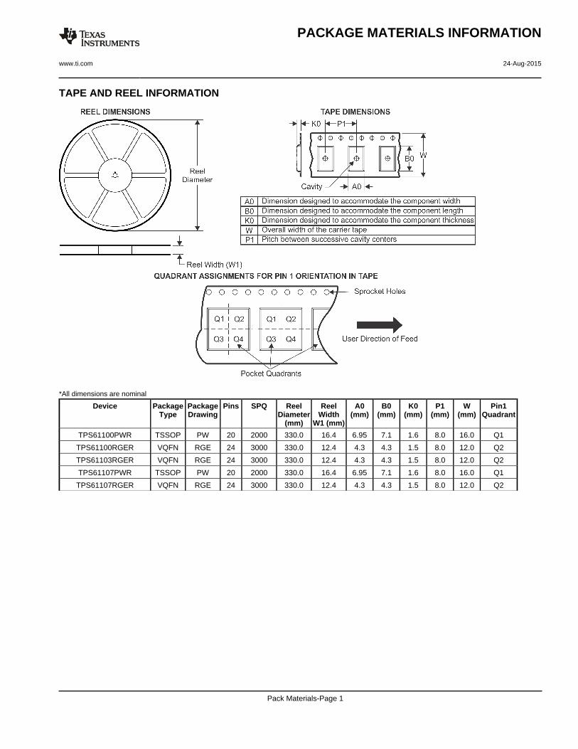
TAPE AND REEL INFORMATION
*All dimensions are nominal
Device PackageType
PackageDrawing
Pins SPQ ReelDiameter
(mm)
ReelWidth
W1 (mm)
A0(mm)
B0(mm)
K0(mm)
P1(mm)
W(mm)
Pin1Quadrant
TPS61100PWR TSSOP PW 20 2000 330.0 16.4 6.95 7.1 1.6 8.0 16.0 Q1
TPS61100RGER VQFN RGE 24 3000 330.0 12.4 4.3 4.3 1.5 8.0 12.0 Q2
TPS61103RGER VQFN RGE 24 3000 330.0 12.4 4.3 4.3 1.5 8.0 12.0 Q2
TPS61107PWR TSSOP PW 20 2000 330.0 16.4 6.95 7.1 1.6 8.0 16.0 Q1
TPS61107RGER VQFN RGE 24 3000 330.0 12.4 4.3 4.3 1.5 8.0 12.0 Q2
PACKAGE MATERIALS INFORMATION
www.ti.com 24-Aug-2015
Pack Materials-Page 1

*All dimensions are nominal
Device Package Type Package Drawing Pins SPQ Length (mm) Width (mm) Height (mm)
TPS61100PWR TSSOP PW 20 2000 367.0 367.0 38.0
TPS61100RGER VQFN RGE 24 3000 338.1 338.1 20.6
TPS61103RGER VQFN RGE 24 3000 338.1 338.1 20.6
TPS61107PWR TSSOP PW 20 2000 367.0 367.0 38.0
TPS61107RGER VQFN RGE 24 3000 338.1 338.1 20.6
PACKAGE MATERIALS INFORMATION
www.ti.com 24-Aug-2015
Pack Materials-Page 2


IMPORTANT NOTICE
Texas Instruments Incorporated and its subsidiaries (TI) reserve the right to make corrections, enhancements, improvements and otherchanges to its semiconductor products and services per JESD46, latest issue, and to discontinue any product or service per JESD48, latestissue. Buyers should obtain the latest relevant information before placing orders and should verify that such information is current andcomplete. All semiconductor products (also referred to herein as “components”) are sold subject to TI’s terms and conditions of salesupplied at the time of order acknowledgment.TI warrants performance of its components to the specifications applicable at the time of sale, in accordance with the warranty in TI’s termsand conditions of sale of semiconductor products. Testing and other quality control techniques are used to the extent TI deems necessaryto support this warranty. Except where mandated by applicable law, testing of all parameters of each component is not necessarilyperformed.TI assumes no liability for applications assistance or the design of Buyers’ products. Buyers are responsible for their products andapplications using TI components. To minimize the risks associated with Buyers’ products and applications, Buyers should provideadequate design and operating safeguards.TI does not warrant or represent that any license, either express or implied, is granted under any patent right, copyright, mask work right, orother intellectual property right relating to any combination, machine, or process in which TI components or services are used. Informationpublished by TI regarding third-party products or services does not constitute a license to use such products or services or a warranty orendorsement thereof. Use of such information may require a license from a third party under the patents or other intellectual property of thethird party, or a license from TI under the patents or other intellectual property of TI.Reproduction of significant portions of TI information in TI data books or data sheets is permissible only if reproduction is without alterationand is accompanied by all associated warranties, conditions, limitations, and notices. TI is not responsible or liable for such altereddocumentation. Information of third parties may be subject to additional restrictions.Resale of TI components or services with statements different from or beyond the parameters stated by TI for that component or servicevoids all express and any implied warranties for the associated TI component or service and is an unfair and deceptive business practice.TI is not responsible or liable for any such statements.Buyer acknowledges and agrees that it is solely responsible for compliance with all legal, regulatory and safety-related requirementsconcerning its products, and any use of TI components in its applications, notwithstanding any applications-related information or supportthat may be provided by TI. Buyer represents and agrees that it has all the necessary expertise to create and implement safeguards whichanticipate dangerous consequences of failures, monitor failures and their consequences, lessen the likelihood of failures that might causeharm and take appropriate remedial actions. Buyer will fully indemnify TI and its representatives against any damages arising out of the useof any TI components in safety-critical applications.In some cases, TI components may be promoted specifically to facilitate safety-related applications. With such components, TI’s goal is tohelp enable customers to design and create their own end-product solutions that meet applicable functional safety standards andrequirements. Nonetheless, such components are subject to these terms.No TI components are authorized for use in FDA Class III (or similar life-critical medical equipment) unless authorized officers of the partieshave executed a special agreement specifically governing such use.Only those TI components which TI has specifically designated as military grade or “enhanced plastic” are designed and intended for use inmilitary/aerospace applications or environments. Buyer acknowledges and agrees that any military or aerospace use of TI componentswhich have not been so designated is solely at the Buyer's risk, and that Buyer is solely responsible for compliance with all legal andregulatory requirements in connection with such use.TI has specifically designated certain components as meeting ISO/TS16949 requirements, mainly for automotive use. In any case of use ofnon-designated products, TI will not be responsible for any failure to meet ISO/TS16949.
Products ApplicationsAudio www.ti.com/audio Automotive and Transportation www.ti.com/automotiveAmplifiers amplifier.ti.com Communications and Telecom www.ti.com/communicationsData Converters dataconverter.ti.com Computers and Peripherals www.ti.com/computersDLP® Products www.dlp.com Consumer Electronics www.ti.com/consumer-appsDSP dsp.ti.com Energy and Lighting www.ti.com/energyClocks and Timers www.ti.com/clocks Industrial www.ti.com/industrialInterface interface.ti.com Medical www.ti.com/medicalLogic logic.ti.com Security www.ti.com/securityPower Mgmt power.ti.com Space, Avionics and Defense www.ti.com/space-avionics-defenseMicrocontrollers microcontroller.ti.com Video and Imaging www.ti.com/videoRFID www.ti-rfid.comOMAP Applications Processors www.ti.com/omap TI E2E Community e2e.ti.comWireless Connectivity www.ti.com/wirelessconnectivity
Mailing Address: Texas Instruments, Post Office Box 655303, Dallas, Texas 75265Copyright © 2015, Texas Instruments Incorporated