Embed Size (px)
Citation preview
TOLERANCE BASED RELIABILITY ANALYSIS OF
AN ANALOG ELECTRIC CIRCUIT
A THESIS SUBMITTED TO
THE GRADUATE SCHOOL OF NATURAL AND APPLIED SCIENCES
OF
MIDDLE EAST TECHNICAL UNIVERSITY
BY
SİNAN ÇAKIR
IN PARTIAL FULFILLMENT OF THE REQUIREMENTS
FOR
THE DEGREE OF MASTER OF SCIENCE
IN
OPERATIONAL RESEARCH
JANUARY 2011
b
Approval of the thesis:
TOLERANCE BASED RELIABILITY ANALYSIS OF
AN ANALOG ELECTRIC CIRCUIT
submitted by SİNAN ÇAKIR in partial fulfillment of the requirements for the degree of Master of Science in Operational Research Department, Middle East Technical University by,
Prof. Dr. Canan Özgen Dean, Graduate School of Natural and Applied Sciences
Prof. Dr. Çağlar Güven Head of Department, Operational Research
Assoc. Prof. Dr. Yasemin Serin Supervisor, Industrial Engineering Dept., METU
Examining Committee Members:
Assoc. Prof. Dr. Canan Sepil Industrial Engineering Dept., METU
Assoc. Prof. Dr. Yasemin Serin Industrial Engineering Dept., METU
Prof. Dr. Meral Azizoğlu Industrial Engineering Dept., METU
Asst. Prof. Dr. Sedef Meral Industrial Engineering Dept., METU
Alper Ünver, M.Sc. Chief Researcher, TÜBİTAK-SAGE
Date:

iii
I hereby declare that all information in this document has been obtained and
presented in accordance with academic rules and ethical conduct. I also declare
that, as required by these rules and conduct, I have fully cited and referenced all
material and results that are not original to this work.
Name, Last Name: Sinan Çakır
Signature :
iv
ABSTRACT
TOLERANCE BASED RELIABILITY ANALYSIS OF
AN ANALOG ELECTRIC CIRCUIT
Çakır, Sinan
M.Sc., Department of Operational Research
Supervisor: Assoc. Prof. Dr. Yasemin Serin
January 2011, 82 pages
This thesis deals with the reliability analysis of a fuel pump driver circuit (FPDC),
which regulates the amount of fuel pumped to a turbojet engine. Reliability
analysis in such critical circuits has great importance since unexpected failures may
cause serious financial loss and even human death.
In this study, two types of reliability analysis are used: “Worst Case Circuit
Tolerance Analysis” (WCCTA) and “Failure Modes and Effects Analysis”
(FMEA). WCCTA involves the analysis of the circuit operation under varying
parameters in their tolerance bands. These parameters include the resistances of the
resistors, operating temperature and voltage input value. The operation of FPDC is
checked and the most critical parameters are determined in the worst case
conditions. While performing WCCTA, a method that guarantees the exact worst
case conditions is used rather than probabilistic methods like Monte Carlo analysis.
The results showed that the parameter variations do not affect the circuit operation
v
unfavorably; operating temperature, voltage input variation and tolerance bands for
the resistances are fairly compatible with the circuit operation.
FMEA is implemented according to the short circuit and open circuit failures of all
the electronic components used in FPDC. The components whose failure has
catastrophic effect on the circuit operation have been determined and some
preventive actions have been offered for some catastrophic failures.
Keywords: Reliability, Worst Case Circuit Analysis, Failure Modes and Effects
Analysis, Analog Circuit Analysis, Tolerance Analysis
vi
ÖZ
BİR ANALOG ELEKTRİK DEVRESİNİN TOLERANS
TABANLI GÜVENİLİRLİK ANALİZİ
Çakır, Sinan
Yüksek Lisans, Yöneylem Araştırması Bölümü
Tez Yöneticisi: Doç. Dr. Yasemin Serin
Ocak 2011, 82 sayfa
Bu tezde bir yakıt pompası sürücü devresinin güvenilirlik analizi
gerçekleştirilmiştir. Bu devre, bir turbojet motora yeterli miktarda yakıt
pompalanmasından sorumludur ve kritik bir öneme sahiptir. Bu türde kritik öneme
sahip devrelerde oluşabilecek beklenmedik hatalar ciddi maddi hasara ve hatta
ölümlere sebep verebileceği için güvenilirlik analizi büyük önem taşımaktadır.
Bu çalışmada, iki tür güvenilirlik analizi gerçekleştirilmiştir: “En Kötü Durum
Devre Tolerans Analizi” (EKDDTA) ve “Hata Türü ve Etkileri Analizi” (HTEA).
EKDDTA ile temel olarak, değişkenler tolerans aralıkları içerisinde değerler
alırken devrenin analizi gerçekleştirilmektedir. Yakıt pompası sürücü devresindeki
karar değişkenleri, direnç değerleri, devrenin çalışma sıcaklığı ve girdideki voltaj
seviyesidir. En kötü durumda devrenin işlevselliği kontrol edilerek en kritik öneme
sahip devre elemanları belirlenmiştir. EKDDTA gerçekleştirilirken Monte Carlo
analizi gibi rassal yöntemler yerine en kötü duruma kesin olarak ulaşmayı sağlayan
bir yöntem kullanılmıştır. Yapılan analizler sonucunda, değişkenlerin tolerans

vii
aralıkları içerisinde aldıkları değerler devrenin işleyişini istenmeyen şekilde
etkilemediği; devrenin çalışma sıcaklığı, girdi voltajı aralığı ve dirençlerin tolerans
aralığının devrenin işleyişi ile uyumlu olduğu gözlenmiştir.
HTEA ise, devredeki elemanların kısa devre ve açık devre hatalarına uğradıkları
durumda devrenin analizinin incelenmesi yoluyla gerçekleştirilmiştir. Yıkıcı etkiye
sebep olacak parça hataları belirlenmiş ve bu hatalardan uygun olanları için
engellemeye yönelik önleyici faaliyetler önerilmiştir.
Anahtar Kelimeler: Güvenilirlik, En Kötü Durum Devre Analizi, Hata Türü ve
Etkileri Analizi, Analog Devre Analizi, Tolerans Analizi

viii
To Ayşegül
and My Family

ix
ACKNOWLEDGMENTS
This thesis work has been completed with the help and support of a considerable
number of people. It is a pleasure for me to have the opportunity to acknowledge
their help and support here. I apologize and express my gratitude to the ones whose
names have not been mentioned in this limited space.
First and foremost, I would like to express my sincere gratitude to Dr. Yasemin
Serin for all her valuable efforts in every step of this thesis. Her encouragement,
support and patience always guided me throughout this period.
My last two years as a research engineer at TÜBİTAK-SAGE have shaped up my
area of interest and my personality. During these two years, I have had the
opportunity to work in a nice environment, which I am greatly indebted to the staff
of the institute and improved myself in many various disciplines. Above all, I have
most felt the encouragement and support of my senior colleagues: Alper Ünver and
Kenan Bozkaya, who have witnessed my thesis work from the beginning and have
been very helpful with their experience and knowledge about the topic. I feel very
lucky to share the same office and work together with them.
This thesis would never be complete without the reviews and comments of the
examining committee, Dr. Canan Sepil, Dr. Meral Azizoğlu and Dr. Sedef Meral.
I appreciate the valuable feedback I have received from them.
I am also grateful to Murat Tunç for all his efforts to explain all the details of the
circuit handled in this study and Ali Karakoç for his valuable aids on the
computational part. Also I would like to thank Melih Çelik for all his supports that
he gave to me, being a new student in the department.

x
I also thank the other residents of 20/15, Şafak Bayram and Kutay Erbayat for
providing me a warm and sincere home environment. Kutay deserves an extra
gratitude for creating a competitive atmosphere and encouraging me to complete
this study just in time.
My family deserves special mention for their everlasting support. I am very
grateful for their trust, understanding and patience.
Last and the most, I would like to express my gratitude to Ayşegül Yılmaz, who
was beside me in the whole period. During my study, my dear Ayşegül never got
tired of encouraging me and I always felt her great support on me. I am
extraordinary fortunate for having her love, patience and confidence.
xi
TABLE OF CONTENTS
ABSTRACT ............................................................................................................. iv
ÖZ............................................................................................................................. vi
ACKNOWLEDGMENTS ........................................................................................ ix
TABLE OF CONTENTS ......................................................................................... xi
LIST OF TABLES ................................................................................................. xiv
LIST OF FIGURES ................................................................................................ xvi
CHAPTERS
1. INTRODUCTION ............................................................................................ 1
1.1. Review of Worst Case Circuit Tolerance Analysis .................................. 2
1.2. Review of the Failure Modes and Effects Analysis.................................. 8
1.3. Reliability Allocation and Prediction ..................................................... 10
1.4. Fault Tree Analysis ................................................................................. 13
2. PRINCIPLES OF ELECTRIC CIRCUIT ANALYSIS .................................. 14
2.1. Current, Voltage and Power ................................................................... 15
2.2. Ground (GND) Node .............................................................................. 16
2.3. Circuit Elements ..................................................................................... 16
2.3.1. Resistor .......................................................................................... 16
2.3.2. Capacitor ....................................................................................... 17
2.3.3. Zener Diode ................................................................................... 17
2.3.4. Bipolar Junction Transistor (BJT) ................................................. 19
xii
2.3.5. Metal Oxide Semiconductor Field Effect Transistor (MOSFET) . 22
2.3.6. Comparator .................................................................................... 24
2.4. Circuit Analysis ...................................................................................... 24
2.4.1. Kirchhoff‟s Voltage Law (KVL)................................................... 24
2.4.2. Kirchhoff‟s Current Law (KCL) ................................................... 25
3. PROBLEM DEFINITION .............................................................................. 26
3.1. Description of the Fuel Pump Driver Circuit (FPDC) ............................ 27
3.2. Problems Under Consideration ............................................................... 29
3.3. Objectives ............................................................................................... 36
3.4. Solution Method ..................................................................................... 37
4. WORST CASE CIRCUIT TOLERANCE ANALYSIS ................................ 40
4.1. Optimization Results .............................................................................. 40
4.1.1. Minimization of VCBb .................................................................... 41
4.1.2. Maximization of VBEb ................................................................... 42
4.1.3. Maximization of VBCa ................................................................... 43
4.1.4. Minimization of (VEBa - VEBaON) ................................................... 44
4.1.5. Maximization of VGSA ................................................................... 46
4.1.6. Minimization of (VDSA - VGSA) ..................................................... 47
4.1.7. Minimization of VGSB .................................................................... 48
4.1.8. Maximization of (VDSB - VGSB) ..................................................... 49
4.2. Interpretation of Optimization Results ................................................... 50
5. FAILURE MODES AND EFFECTS ANALYSIS ........................................ 52
5.1. Short Circuit Failure ............................................................................... 53
5.2. Open Circuit Failure ............................................................................... 53
5.3. FMEA Matrix ......................................................................................... 53
5.4. FMEA Results ........................................................................................ 56

xiii
5.4.1. Short Circuit Failure of R1 ............................................................ 57
5.4.2. Short Circuit Failure of R2 ............................................................ 58
5.4.3. Short Circuit Failure of R3 ............................................................ 58
5.4.4. Short Circuit Failure of R4 ............................................................ 59
5.4.5. Short Circuit Failure of R5 ............................................................ 60
5.4.6. Short Circuit Failure of R6 ............................................................ 61
5.4.7. Open Circuit Failure of R7 ............................................................ 61
5.4.8. Short Circuit Failure of R8 ............................................................ 62
5.4.9. Short Circuit Failure of R9 ............................................................ 63
5.4.10. Open Circuit Failure of Z1 .......................................................... 64
5.4.11. Open Circuit Failure of Z2 .......................................................... 65
5.5. Interpretation of FMEA Results ............................................................. 66
6. CONCLUSION .............................................................................................. 71
REFERENCES ................................................................................................... 75
APPENDIX A. CODE DESCRIPTIONS .......................................................... 77
xiv
LIST OF TABLES
TABLES
Table 1.1. Fault Set of Video Amplifier Circuit [9] .................................................. 9
Table 1.2. Temperature Factors for Low Frequency FET Type ............................. 12
Table 2.1. BJT Operating Regions and Voltage Requirements .............................. 21
Table 2.2. MOSFET Operating Regions and Voltage Requirements ..................... 23
Table 2.3. MOSFET Current Characteristics in Different Operating Regions ....... 23
Table 3.1. Descriptions of Uncontrollable Variables .............................................. 30
Table 3.2. Intervals of Decision Variables .............................................................. 31
Table 3.3. Parameters and Constants Used in the Constraints ................................ 32
Table 3.4. Constraints.............................................................................................. 33
Table 3.5. Assumed Transistor Operating Regions and Required Conditions........ 36
Table 3.6. Objective Functions and Check Conditions ........................................... 37
Table 4.1. Binding Constraints for Min. VCBb......................................................... 41
Table 4.2. Binding Constraints for Max. VBEb Problem ......................................... 43
Table 4.3. Binding Constraints for Max. VBCa Problem ......................................... 44
Table 4.4. Binding Constraints for Min. (VEBa – VEBaON) Problem ........................ 45
Table 4.5. Binding Constraints for Max. VGSA Problem ......................................... 47
Table 4.6. Binding Constraints for Max. (VDSA-VGSA) Problem ............................. 48
Table 4.7. Binding Constraints for Max. VGSB Problem ......................................... 49
Table 4.8. Binding Constraints for Max. VGSB Problem ......................................... 50
Table 4.9. Pout and T Values at Optimum Value of Each Objective ....................... 51
Table 5.1. Short and Open Circuit Failures Examination ....................................... 54
Table 5.2. Failures That Will Be Analyzed Computationally ................................. 55
Table 5.3. New Objectives, When to Use and Their Check Conditions ................. 56
xv
Table 5.4. Short Circuit Failure Effect of R1........................................................... 57
Table 5.5. Short Circuit Failure Effect of R2........................................................... 58
Table 5.6. Short Circuit Failure Effect of R3........................................................... 59
Table 5.7. Short Circuit Failure Effect of R4........................................................... 60
Table 5.8. Short Circuit Failure Effect of R5........................................................... 60
Table 5.9. Short Circuit Failure Effect of R6........................................................... 61
Table 5.10. Open Circuit Failure Effect of R7......................................................... 62
Table 5.11. Short Circuit Failure Effect of R8......................................................... 63
Table 5.12. Short Circuit Failure Effect of R9......................................................... 63
Table 5.13. Open Circuit Failure Effect of Z1 ......................................................... 65
Table 5.14. Open Circuit Failure Effect of Z2 ......................................................... 66
Table 5.15. Revised FMEA Matrix ......................................................................... 67
Table 5.16. Failure Distributions According to FMD-97 ....................................... 68
xvi
LIST OF FIGURES
FIGURES
Figure 1.1. Distribution & Histogram of Overcurrent Circuit Output for Normal
Tolerance Parts [12] ............................................................................................. 5
Figure 1.2. Distribution & Histogram of Overcurrent Circuit Output for Tight
Tolerance Parts [12] ............................................................................................. 5
Figure 1.3. Sensitivity over Various Frequency Levels [8] ...................................... 6
Figure 1.4. Step Response of the Inductor Lx [2] ...................................................... 7
Figure 1.5. Open and Short Circuit Failure Simulation [5] ..................................... 10
Figure 1.6. Sample Fault Tree ................................................................................. 13
Figure 2.1. Schematic Representation of Fuel Pump Driver Circuit ...................... 15
Figure 2.2. Schematic Representation of a Resistor................................................ 16
Figure 2.3. Schematic Representations of a Capacitor............................................ 17
Figure 2.4. Schematic Representation of a Zener Diode......................................... 18
Figure 2.5. I-V Characteristics of a Diode .............................................................. 18
Figure 2.6. Schematic Representations of NPN and PNP type BJT‟s .................... 19
Figure 2.7. Operating Modes of a NPN Transistor ................................................. 20
Figure 2.8. VBE(on) vs. IC Characteristics of ZXTN2063E6 BJT “b” ....................... 21
Figure 2.9. Schematic Representations of MOSFET Transistors ........................... 22
Figure 2.10. KVL Loop Example............................................................................ 25
Figure 2.11. KCL Node Example............................................................................ 25
Figure 3.1. Schematic Representation of Fuel Pump Driver Circuit ...................... 27
Figure 3.2. Relationship Between the Circuit and Other Elements ........................ 28
Figure 3.3. VBEaON vs. ICa Characteristics [17] ........................................................ 36
Figure 3.4. Optimization Flowchart ........................................................................ 38
Figure 3.5. ModeFRONTIER File Graphical Interface .......................................... 39
xvii
Figure 4.1. Minimized VCBb vs. Pout Characteristics under varying T and R1…R9
variables .............................................................................................................. 41
Figure 4.2. Maximized VBEb vs. Pout Characteristics under varying T and R1…R9
variables .............................................................................................................. 42
Figure 4.3. Maximized VBCa vs. Pout Characteristics under varying T and R1…R9
variables .............................................................................................................. 43
Figure 4.4. Minimized (VEBa – VEBaON) vs. Pout Characteristics under varying T and
R1…R9 variables ................................................................................................. 44
Figure 4.5. Minimized (VEBa – VEBaON) vs. Pout Characteristics under varying T and
R1…R9 variables (R4, R5, R6, R8 and R9 with 1% tolerance band) ..................... 46
Figure 4.6. Maximized VGSA vs. Pout Characteristics under varying T and R1…R9
variables .............................................................................................................. 46
Figure 4.7. Minimized (VDSA-VGSA) vs. Pout Characteristics under varying T and
R1…R9 variables ................................................................................................. 47
Figure 4.8. Minimized VGSB vs. Pout Characteristics under varying T and R1…R9
variables .............................................................................................................. 48
Figure 4.9. Maximized (VDSB - VGSB) vs. Pout Characteristics under varying T and
R1…R9 variables ................................................................................................. 49
Figure 5.1. Preventive Action for Open Circuit Failure of Z1................................. 69
Figure 5.2. Preventive Action for Open Circuit Failure of Z2................................. 69
1
CHAPTER 1
INTRODUCTION
In today‟s competitive world, reliability is a very important concept in electric
circuits, which may be considered as the brain of many technological devices.
There are many factors that affect the reliability of a circuit. Also there is a list of
issues like cost, logistics, usability etc. required to be considered while keeping the
reliability at high levels. However, ensuring a high reliability must be the primary
concern in the circuits that have critical tasks. Therefore, reliability analysis should
be performed on all circuitry that is safety critical. Most effective actions to make a
circuit more reliable are taken in the design phase by following the advised
procedures and performing various reliability analyses. There are many reliability
analysis methods, like worst case circuit tolerance analysis, failure modes and
effects analysis, fault tree analysis, reliability allocation and prediction. In this
study, worst case circuit tolerance analysis and failure modes and effects analysis
of a fuel pump driver circuit will be performed. This circuit has a very critical
mission, which is supplying the required amount of fuel to a turbojet engine. In
case of a failure; the air vehicle, whose thrust is created by the amount of the fuel
pumped, is subject to fall.
Worst case circuit analysis takes the component variability into consideration and
investigates the circuit operation under the worst case conditions, which consists of
most extreme environmental and operating conditions. Temperature, radiation and
humidity can be considered as the most effective environmental factors and the
worst case operating conditions are usually formed by the external electrical inputs.
2
Failure modes and effect analysis is another important analysis method used in
circuit reliability analysis. In this analysis, the failure mechanisms of the
components and their effects on the circuit operation are examined. With this
analysis, it is aimed to design robust circuits, which can even withstand failures of
some components in the circuit.
Both worst case circuit analysis and failure modes and effects analysis must be
performed in the design phase to take the necessary actions at the right time.
Several actions, like modifying the circuit design, adding new components or
changing the components used in the circuit, can be taken to make a circuit more
reliable. In the design phase, the designer has more flexibility and the modifications
will not increase the cost significantly. However, if the reliability analyses are
skipped in the design phase and a major defect is realized after the manufacturing
phase, it will have a huge effect on the cost of the project and surely the customer
satisfaction will decrease. Catastrophic failures may even cost a human‟s life.
Hereafter, review on the worst case circuit tolerance analysis and failure modes and
effects analysis, both of which are applied to the fuel pump driver circuit, will be
given. Furthermore, brief information about the fault tree analysis, reliability
allocation and prediction will be supplied.
1.1. Review of Worst Case Circuit Tolerance Analysis
Worst case circuit tolerance analysis is performed under the toughest
environmental and operating conditions, while the component variables take value
in their tolerance bands. However, finding the worst case conditions is the
challenging part of this analysis. There are various methods generated for this
purpose and these methods will be described below.
Worst case circuit analysis can be performed in time and frequency domain
depending on the operation of the circuit under consideration. Actually, in which
domain the circuit is to be analyzed in is determined by the circuit itself.
The analyses performed in time domain can be classified in two topics: Transient
analyses, which focuses on the circuit timing during the transitions and the steady
3
state analyses, which investigate the circuit operation after all the transients are
finished.
If the worst case is analyzed in frequency domain, time is not considered and the
circuit operation is analyzed under various frequencies. Not whole of the electronic
circuits can be analyzed in frequency domain, since the signal that runs through the
circuit must be oscillating with a frequency for the circuit to be analyzed in
frequency domain. However, this is not the case in all the circuits.
Most common method for the worst case circuit analysis is the well-known Monte
Carlo method. Monte Carlo method is a stochastic method and used frequently in
SPICE (Simulation Program with Integrated Circuit Emphasis) programs, which
simulate the circuit operation depending on the simulation models of the
components used in the circuit. However, it is not guaranteed to reach the worst
case conditions in the circuit with this method due to its probabilistic nature. To
approach the worst case conditions, performing very large numbers of Monte Carlo
simulation may be required.
“Tolerance Design of Electronic Circuits” composed by Spence and Soin [7] is a
very good reference for understanding tolerance based circuit design and analysis.
In this book, the authors started with presenting general concepts and
representations for tolerance design and analysis. They supplied an overview of
tolerance design for various circuit types and explained Monte Carlo tolerance
analysis method with supportive examples. Finally, they gave suggestions for
circuit performance calculations and dealt with the use of sensitivity analysis.
“Worst Case Circuit Analysis Application Guidelines” published by Reliability
Information Analysis Center (RIAC) [16] is as well a good reference particularly
for the worst case circuit tolerance analysis. In this document, worst case circuit
analysis techniques and methods are reviewed and the worst case analyses of an
analog circuit and a digital circuit have been performed. The analysis of the analog
circuit has been made with three different methods: Extreme value analysis,
root-sum-squared analysis, Monte Carlo analysis and the results obtained with each
method are compared, in order to observe their successes in determining circuit
4
performance. In digital circuit analysis, worst case analysis is based on the timing
parameters and required delay times in the circuit. Extreme value analysis, which is
the only applicable method in this case, has been used for the analysis.
In the literature, there are a number of studies, in which the worst case analyses of
various circuits are performed. Most outstanding studies can be listed as follows:
Tian and Shi [8] and Dreyer [1] performed the worst case analyses of electronic
circuits in frequency domain while generating new algorithms to reach the worst
case conditions. Likewise, Femia and Spagnuolo [2] and Tian and Ling [9]
investigated the operations of various circuits in time domain. Kolev [4] generated
a method to reach the exact worst case solution in the time domain. However, the
majority of the studies in the worst case circuit analysis concentrate on the
frequency domain analysis since it is fairly easier and is a more applicable analysis
method.
The earliest studies that could be found about the effect of the components‟
tolerance on the circuit performance are White‟s papers: “Introduction to Six
Sigma with a Design Example” [11] and its continuation study, “Component
Tolerance and Circuit Performance: A Case Study” [12] . In these studies, main
aim is to reach six sigma quality by choosing electronic components with adequate
tolerance bands. In these studies, a simple overcurrent detector circuit has been
analyzed and Monte Carlo simulation method has been used. White used uniform
distribution for the components‟ tolerances in [11], then he repeated the same study
in [12] with normal distribution. White has approached the problem with a
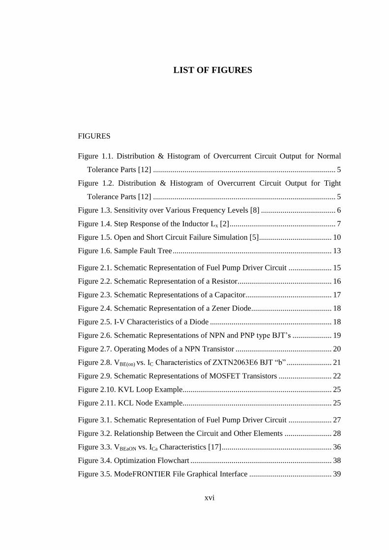
statistical point of view and constituted the following distributions as shown in
Figure 1.1 and Figure 1.2.
5
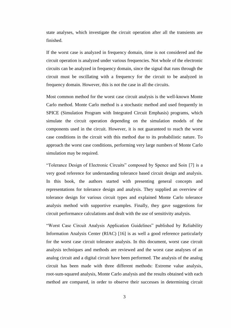
Figure 1.1. Distribution & Histogram of Overcurrent Circuit Output for
Normal Tolerance Parts [12]
Figure 1.2. Distribution & Histogram of Overcurrent Circuit Output for Tight
Tolerance Parts [12]
Figure 1.1 and Figure 1.2 shows the effect of normal and tight tolerances on the
circuit performance. In his paper, White also compared the results obtained for
normally distributed components values with the uniformly distributed components
in [12] and concluded that more realistic results are obtained with normally
distributed tolerances.
In 1996, Tian and Ling [9] have improved two complementary algorithms:
Analytical and accurate algorithms to obtain the worst case solutions. While the
analytical algorithm is faster than the accurate algorithm, it comprises more interval
expansion error. They applied their algorithms both in time domain and frequency
6
domain and compared the results obtained with the analytical and accurate
algorithms.
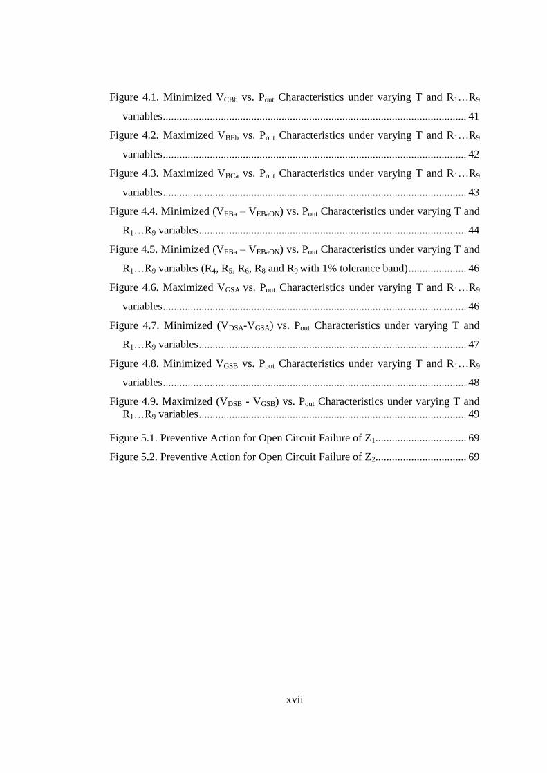
Tian and Shi [8] took various circuits in their study and made their analyses in
frequency domain. They defined the monotonicity concept and performed their
worst case analysis checking the monotonicity condition of the relevant function.
According to Tian and Shi, a function is monotonic if this function is
monotonically decreasing or increasing due to the changes in the parameter space,
where the parameters are defined in an interval. After the specified algorithms are
run, the sensitivities of the voltage or current levels according to the components in
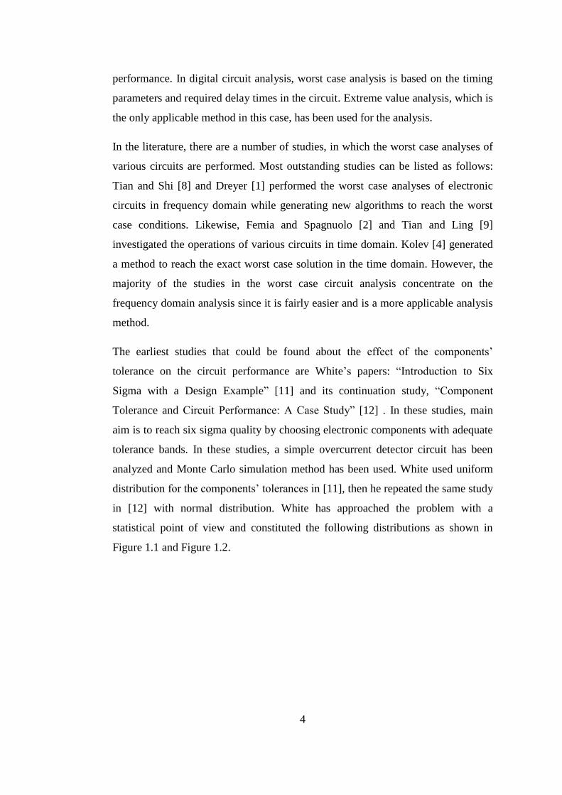
the circuit are drawn in frequency domain. Figure 1.3 shows the sensitivity of
voltage, V(2) versus circuit parameter R over the parameter space.
Figure 1.3. Sensitivity over Various Frequency Levels [8]
Dreyer [1] focused on the worst case analysis of integrated circuits and performed
his analyses with successive application of the interval-valued Sherman-Morrison
formula. In his study, he dealt with an operational amplifier, which includes several
transistors and resistors inside. However, he simplified the circuit scheme by using
the small-circuit equivalent schematics for the transistors and supplied the
sensitivity analysis result in frequency domain like Tian and Shi [8].
Kolev [4] generated a method to reach the exact worst case solution. While
reaching the exact solution, inner and outer solutions are found first and the exact
7
solution is determined if the certain monotonicity conditions are fulfilled. He
applied his methods to a notch filter circuit. Although this circuit can be analyzed
in frequency domain, he has chosen to analyze it in time domain. By fixing the
operating frequency of the circuit, the transient analysis is performed according to
the methods he generated.
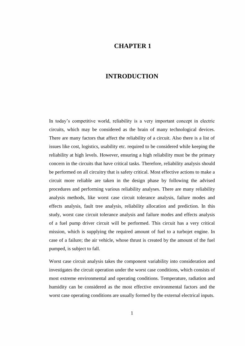
Femia and Spagnuolo [2] also performed analyses in time domain, however with
fairly different methodology. Like Kolev, they also aimed to reach the exact or
with their words, „true‟ worst case conditions with a new approach. Their method is
based on the joint usage of genetic algorithms and affine arithmetic. They offered
the usage of genetic algorithms to reach the inner solution and minimize the
underestimation error obtained in stochastic methods. Likewise, affine arithmetic is
used to reach the outer solution and minimize the overestimation errors obtained
with the interval arithmetic methods. They performed the transient analyses of
various circuits and compared their results with the Monte-Carlo analysis results. In
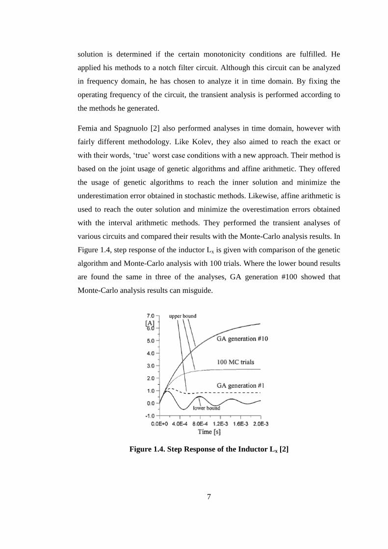
Figure 1.4, step response of the inductor Lx is given with comparison of the genetic
algorithm and Monte-Carlo analysis with 100 trials. Where the lower bound results
are found the same in three of the analyses, GA generation #100 showed that
Monte-Carlo analysis results can misguide.
Figure 1.4. Step Response of the Inductor Lx [2]
8
In this thesis, the exact or true worst case conditions are aimed and instead of using
Monte Carlo simulation method, a deterministic optimization model that ensures to
reach the worst case is constructed. This model is solved using MATLAB and
ModeFRONTIER softwares. The worst case circuit tolerance analysis is performed
according to:
- Resistance variations within the tolerance bands
- Operating temperature interval of the circuit (environmental condition)
- Voltage input variations (operating condition)
In the reliability analysis of the fuel pump driver circuit, the operating region of the
transistors are taken as base and the effects of component variability, temperature
and the voltage input are assessed by checking the operating regions of the
transistors if they remain in their desired regions. In the literature, no study that
considers the operating regions of the transistors and performs the reliability
analyses according to these conditions has been found to our best knowledge.
Dreyer [1] and Tien and Ling [9] performed the worst case analysis of circuits that
include transistors in their scheme. However, in their analyses they used the small
signal models for the transistors, which simulate the operation of the transistors
only while they are operating in small currents.
1.2. Review of the Failure Modes and Effects Analysis
Failure modes and effect analysis is another important concept in circuit reliability
analysis. By applying this method, it is aimed to examine the effects of the
components‟ failures in the circuit. Each component has different failure modes
with different probabilities. Most common failure modes can be listed as follows:
- Open circuit
- Short circuit
- Part-parameter shift
- Dielectric breakdown
- Wear
9
This analysis method is well defined in U.S. military document MIL-HDBK-338B
[13] and the failure distributions for each part are given in FMD-97 document [15].
These two documents constitute a base for FMEA and are taken into consideration
in the FMEA studies done in this thesis. Depending on the FMEA results, the weak
parts of the circuit in issue have been determined and some modifications to
minimize the number of catastrophic and critical circuit failures have been
suggested.
In the literature, there are two outstanding studies that are fairly related with the
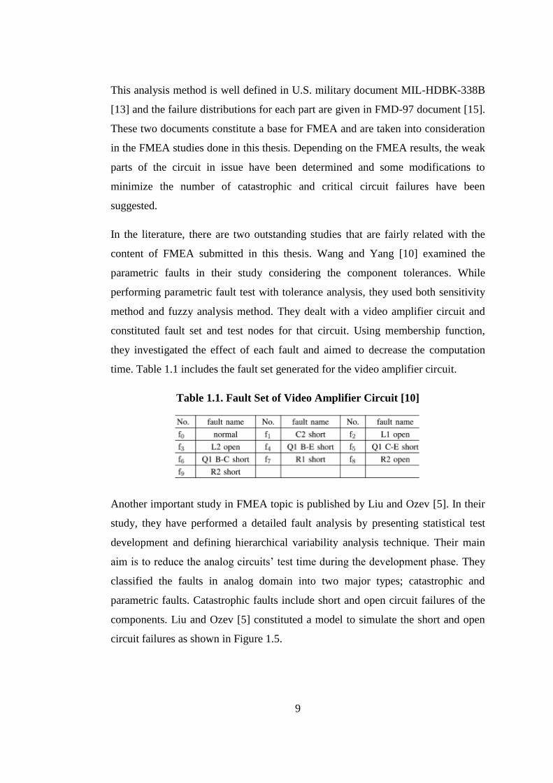
content of FMEA submitted in this thesis. Wang and Yang [10] examined the
parametric faults in their study considering the component tolerances. While
performing parametric fault test with tolerance analysis, they used both sensitivity
method and fuzzy analysis method. They dealt with a video amplifier circuit and
constituted fault set and test nodes for that circuit. Using membership function,
they investigated the effect of each fault and aimed to decrease the computation
time. Table 1.1 includes the fault set generated for the video amplifier circuit.
Table 1.1. Fault Set of Video Amplifier Circuit [10]
Another important study in FMEA topic is published by Liu and Ozev [5]. In their
study, they have performed a detailed fault analysis by presenting statistical test
development and defining hierarchical variability analysis technique. Their main
aim is to reduce the analog circuits‟ test time during the development phase. They
classified the faults in analog domain into two major types; catastrophic and
parametric faults. Catastrophic faults include short and open circuit failures of the
components. Liu and Ozev [5] constituted a model to simulate the short and open
circuit failures as shown in Figure 1.5.
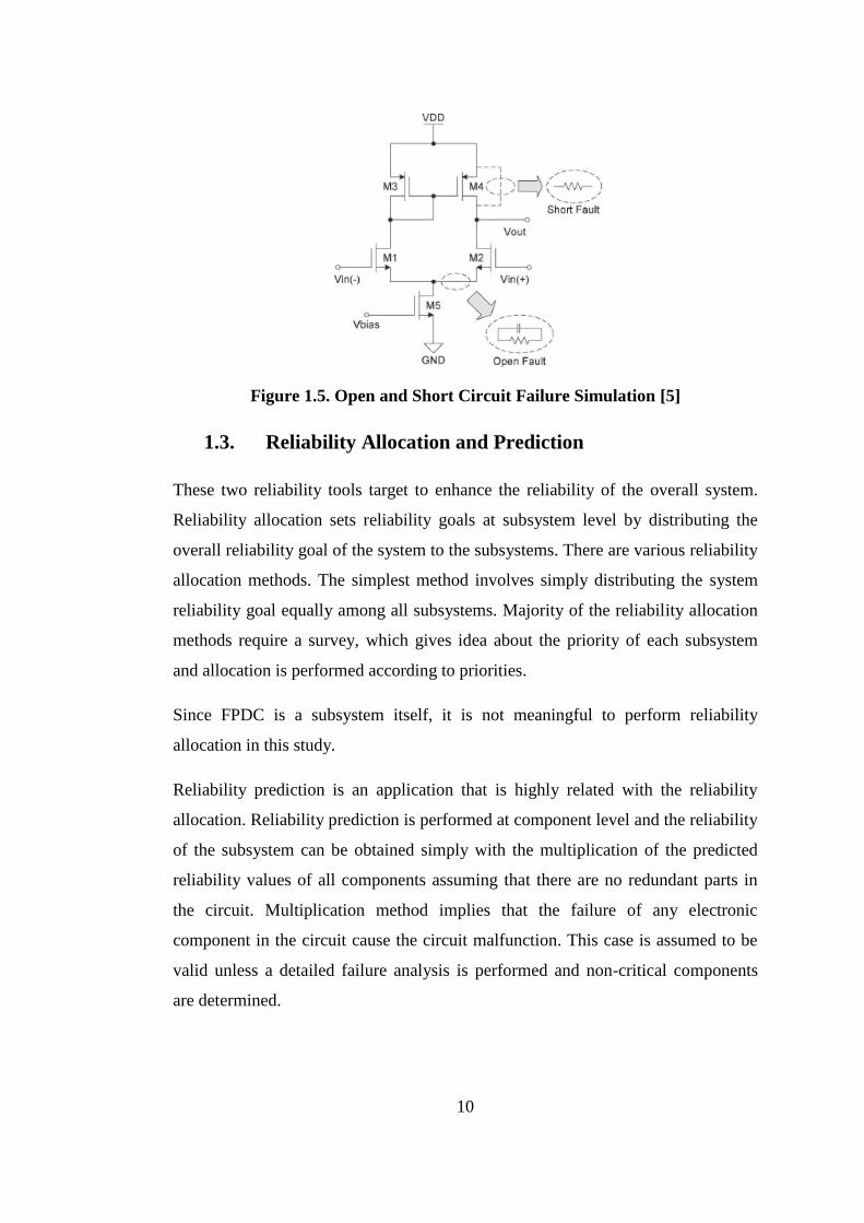
10
Figure 1.5. Open and Short Circuit Failure Simulation [5]
1.3. Reliability Allocation and Prediction
These two reliability tools target to enhance the reliability of the overall system.
Reliability allocation sets reliability goals at subsystem level by distributing the
overall reliability goal of the system to the subsystems. There are various reliability
allocation methods. The simplest method involves simply distributing the system
reliability goal equally among all subsystems. Majority of the reliability allocation
methods require a survey, which gives idea about the priority of each subsystem
and allocation is performed according to priorities.
Since FPDC is a subsystem itself, it is not meaningful to perform reliability
allocation in this study.
Reliability prediction is an application that is highly related with the reliability
allocation. Reliability prediction is performed at component level and the reliability
of the subsystem can be obtained simply with the multiplication of the predicted
reliability values of all components assuming that there are no redundant parts in
the circuit. Multiplication method implies that the failure of any electronic
component in the circuit cause the circuit malfunction. This case is assumed to be
valid unless a detailed failure analysis is performed and non-critical components
are determined.
11
Obtained reliability prediction results are compared with reliability allocation
values and it is checked if the target values hold. Thus, actions to enhance
reliability are taken at the design phase. However, it must be kept in mind that
reliability prediction values are only approximated values and do not reflect the real
reliability values, which can only be obtained by performing appropriate reliability
tests.
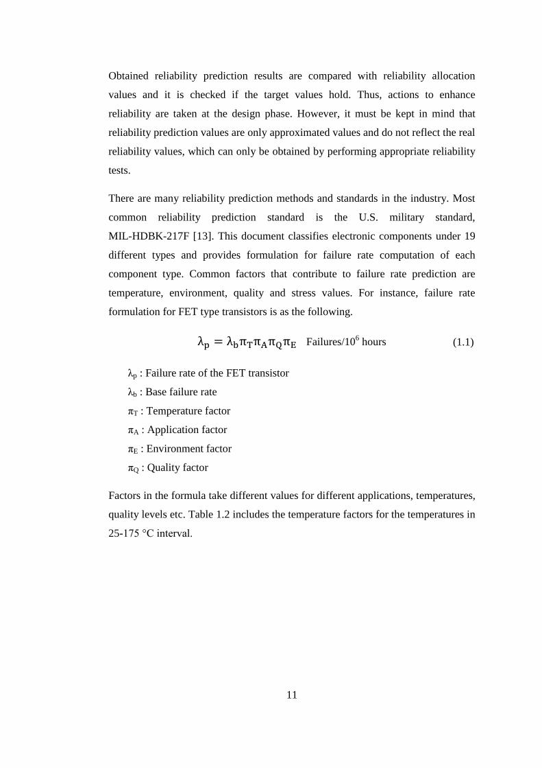
There are many reliability prediction methods and standards in the industry. Most
common reliability prediction standard is the U.S. military standard,
MIL-HDBK-217F [13]. This document classifies electronic components under 19
different types and provides formulation for failure rate computation of each
component type. Common factors that contribute to failure rate prediction are
temperature, environment, quality and stress values. For instance, failure rate
formulation for FET type transistors is as the following.
Failures/106 hours
λp : Failure rate of the FET transistor
λb : Base failure rate
πT : Temperature factor
πA : Application factor
πE : Environment factor
πQ : Quality factor
Factors in the formula take different values for different applications, temperatures,
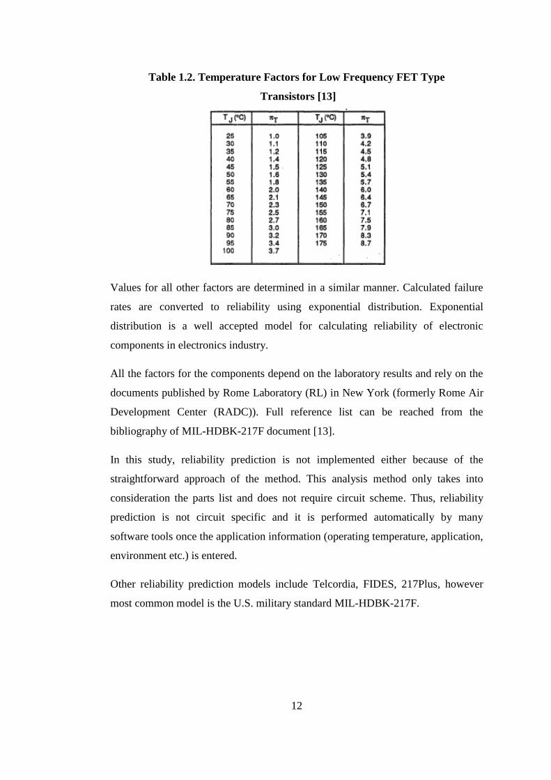
quality levels etc. Table 1.2 includes the temperature factors for the temperatures in
25-175 °C interval.
(1.1)
12
Table 1.2. Temperature Factors for Low Frequency FET Type
Transistors [13]
Values for all other factors are determined in a similar manner. Calculated failure
rates are converted to reliability using exponential distribution. Exponential
distribution is a well accepted model for calculating reliability of electronic
components in electronics industry.
All the factors for the components depend on the laboratory results and rely on the
documents published by Rome Laboratory (RL) in New York (formerly Rome Air
Development Center (RADC)). Full reference list can be reached from the
bibliography of MIL-HDBK-217F document [13].
In this study, reliability prediction is not implemented either because of the
straightforward approach of the method. This analysis method only takes into
consideration the parts list and does not require circuit scheme. Thus, reliability
prediction is not circuit specific and it is performed automatically by many
software tools once the application information (operating temperature, application,
environment etc.) is entered.
Other reliability prediction models include Telcordia, FIDES, 217Plus, however
most common model is the U.S. military standard MIL-HDBK-217F.
13
1.4. Fault Tree Analysis
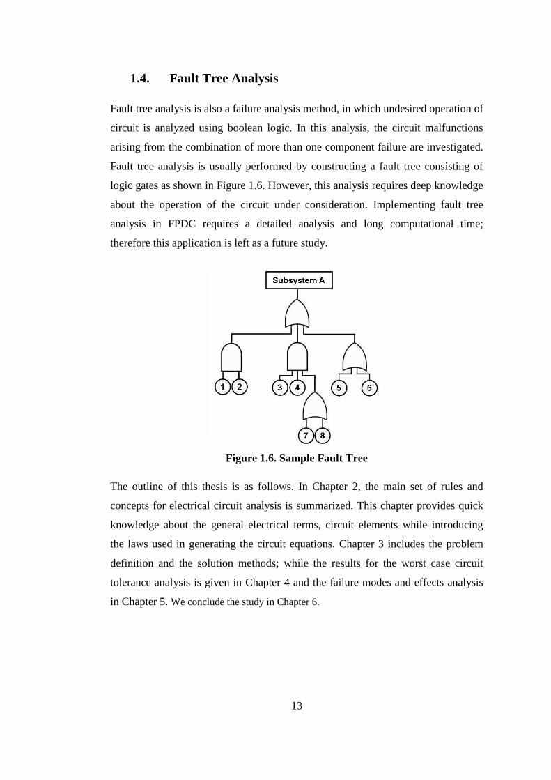
Fault tree analysis is also a failure analysis method, in which undesired operation of
circuit is analyzed using boolean logic. In this analysis, the circuit malfunctions
arising from the combination of more than one component failure are investigated.
Fault tree analysis is usually performed by constructing a fault tree consisting of
logic gates as shown in Figure 1.6. However, this analysis requires deep knowledge
about the operation of the circuit under consideration. Implementing fault tree
analysis in FPDC requires a detailed analysis and long computational time;
therefore this application is left as a future study.
Figure 1.6. Sample Fault Tree
The outline of this thesis is as follows. In Chapter 2, the main set of rules and
concepts for electrical circuit analysis is summarized. This chapter provides quick
knowledge about the general electrical terms, circuit elements while introducing
the laws used in generating the circuit equations. Chapter 3 includes the problem
definition and the solution methods; while the results for the worst case circuit
tolerance analysis is given in Chapter 4 and the failure modes and effects analysis
in Chapter 5. We conclude the study in Chapter 6.
14
CHAPTER 2
PRINCIPLES OF ELECTRIC CIRCUIT ANALYSIS
There are many different elements in an electronic circuit and each of these
elements has several parameters that affect the circuit‟s performance. However,
most of these parameters vary due to imperfect manufacturing process. In this
study, we investigate the operation of an electronic circuit which controls the
power supply of a fuel pump that is responsible from pumping fuel to a turbojet
engine when the control variables are in their tolerance bands while proposing an
alternative methodology to basic circuit simulation methods.
In Figure 2.1, the schematic of the Fuel Pump Driver Circuit is shown. In this
circuit, there are 6 different elements, each of which contributes to the circuit‟s
performance in various ways. They are:
1) Resistor
2) Capacitor
3) Bipolar Junction Transistor (BJT)
4) Metal Oxide Semiconductor Field Effect Transistor (MOSFET)
5) Zener Diode
6) Comparator
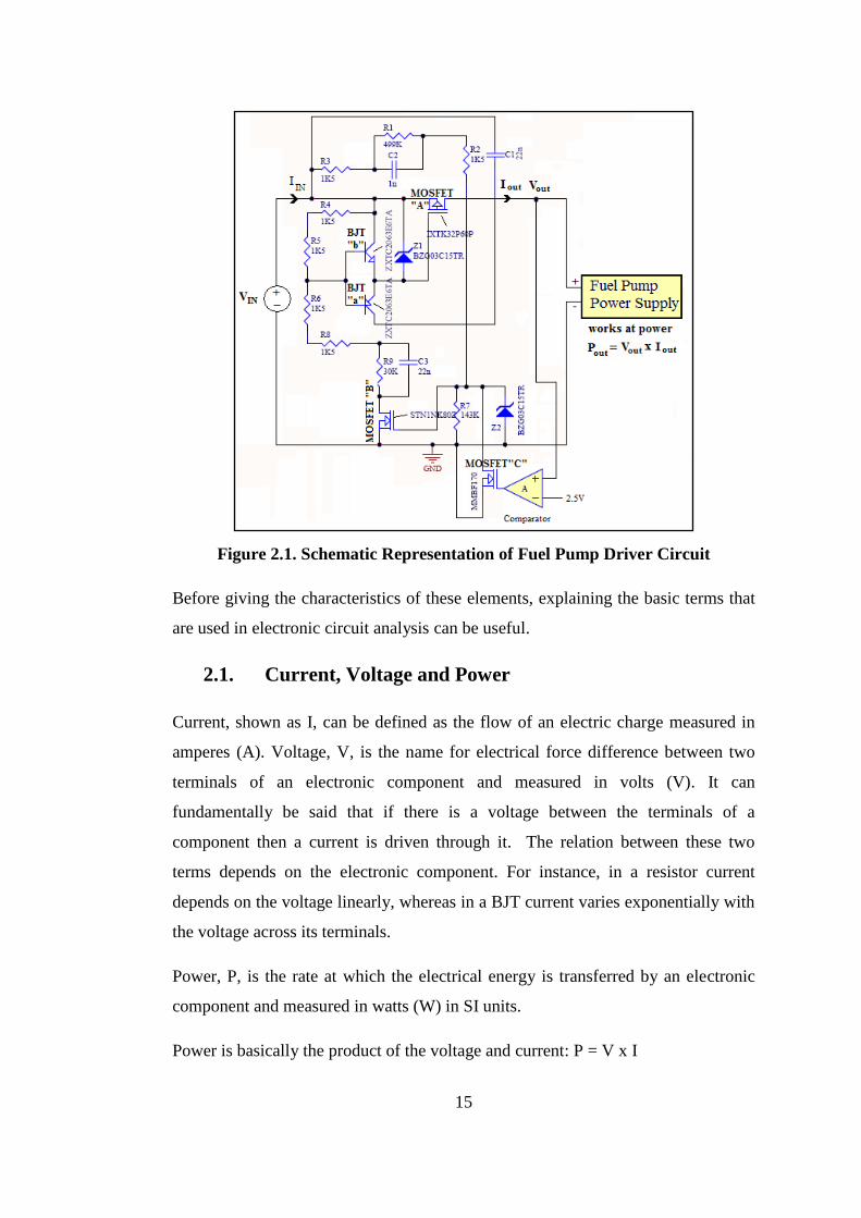
15
Figure 2.1. Schematic Representation of Fuel Pump Driver Circuit
Before giving the characteristics of these elements, explaining the basic terms that
are used in electronic circuit analysis can be useful.
2.1. Current, Voltage and Power
Current, shown as I, can be defined as the flow of an electric charge measured in
amperes (A). Voltage, V, is the name for electrical force difference between two
terminals of an electronic component and measured in volts (V). It can
fundamentally be said that if there is a voltage between the terminals of a
component then a current is driven through it. The relation between these two
terms depends on the electronic component. For instance, in a resistor current
depends on the voltage linearly, whereas in a BJT current varies exponentially with
the voltage across its terminals.
Power, P, is the rate at which the electrical energy is transferred by an electronic
component and measured in watts (W) in SI units.
Power is basically the product of the voltage and current: P = V x I
16
2.2. Ground (GND) Node
This node is the reference node in a circuit which is basically assumed to have “0”
voltage so that all the elements in the circuit will function correctly having the
same point of reference.
2.3. Circuit Elements
The operations of the electronic components used in the circuit are summarized
below.
2.3.1. Resistor
Resistor is a two terminal electronic component that produces voltage across its
terminals. It can be used for maintaining the voltage at a terminal at desired levels
or regulating the current that flows through a path to a desired level. Actually,
resistors are very basic circuit elements and used for many purposes in electronic
circuits. The main characteristics of a resistor are its resistance, tolerance and
power rating. The resistance is represented with letter “R” and the SI unit for it is
“ohm” (Ω). Figure 2.2 shows a schematic representation of a resistor.
Figure 2.2. Schematic Representation of a Resistor
The behavior of an ideal resistor is dictated by the relationship specified in Ohm‟s
law:
V = I x R
As can be figured from the formula, in a resistor current through a resistor varies
linearly with the voltage across its terminals.
Resistors as manufactured are subject to a certain percentage tolerance. This
tolerance may be as low as 0.01% of the resistance or up high like 5% or even
(2.1)
17
10%. Using a resistor with a tight tolerance can make the design more robust, but it
slightly increases cost. However choosing a resistor with a wide tolerance, thus
with a lower cost, may cause the circuit fail in some cases. In this study, the
tolerance for all the resistors are 5% and the analyses are carried out for the varying
resistance values within this 5% tolerance band.
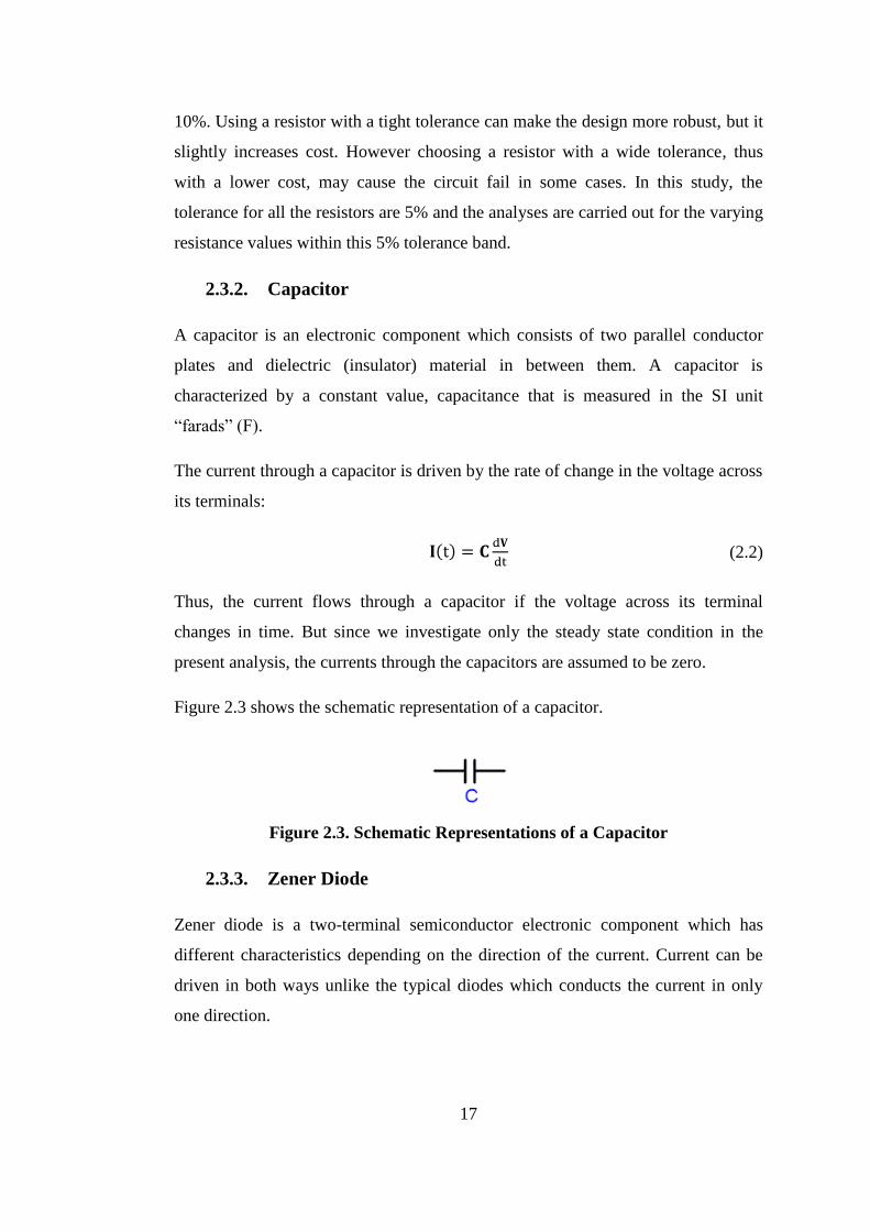
2.3.2. Capacitor
A capacitor is an electronic component which consists of two parallel conductor
plates and dielectric (insulator) material in between them. A capacitor is
characterized by a constant value, capacitance that is measured in the SI unit
“farads” (F).
The current through a capacitor is driven by the rate of change in the voltage across
its terminals:
Thus, the current flows through a capacitor if the voltage across its terminal
changes in time. But since we investigate only the steady state condition in the
present analysis, the currents through the capacitors are assumed to be zero.
Figure 2.3 shows the schematic representation of a capacitor.
Figure 2.3. Schematic Representations of a Capacitor
2.3.3. Zener Diode
Zener diode is a two-terminal semiconductor electronic component which has
different characteristics depending on the direction of the current. Current can be
driven in both ways unlike the typical diodes which conducts the current in only
one direction.
(2.2)
18
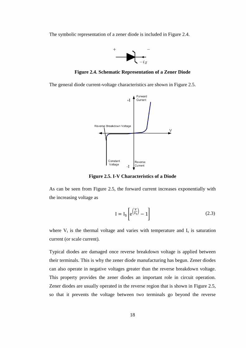
The symbolic representation of a zener diode is included in Figure 2.4.
Figure 2.4. Schematic Representation of a Zener Diode
The general diode current-voltage characteristics are shown in Figure 2.5.
Figure 2.5. I-V Characteristics of a Diode
As can be seen from Figure 2.5, the forward current increases exponentially with
the increasing voltage as
where Vt is the thermal voltage and varies with temperature and Is is saturation
current (or scale current).
Typical diodes are damaged once reverse breakdown voltage is applied between
their terminals. This is why the zener diode manufacturing has begun. Zener diodes
can also operate in negative voltages greater than the reverse breakdown voltage.
This property provides the zener diodes an important role in circuit operation.
Zener diodes are usually operated in the reverse region that is shown in Figure 2.5,
so that it prevents the voltage between two terminals go beyond the reverse
(2.3)
19
breakdown voltage and contributes to the circuit operation with that valuable
property.
Unfortunately, a general formula that characterizes the reverse current does not
exist. Reverse current vs. the voltage characteristics can only be obtained from
circuit simulation tools. That is how the reverse characteristics of BZG03C15
coded zener diode which is used in our circuit are generated.
2.3.4. Bipolar Junction Transistor (BJT)
A Bipolar Junction Transistor is a three terminal semiconductor electronic
component. It can be used in different circuit applications like switching and
amplifying, that is, increasing the input current in the output.
BJT‟s have two different types: NPN and PNP. The operations of these two types
of BJT‟s are slightly different. The schematics of NPN and PNP are given in
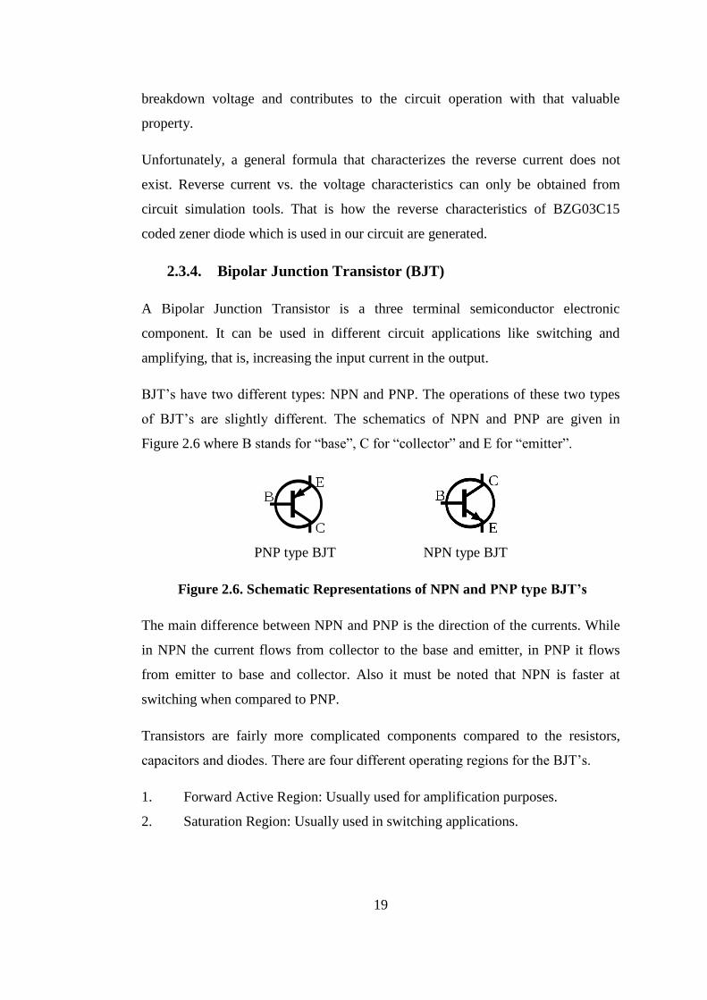
Figure 2.6 where B stands for “base”, C for “collector” and E for “emitter”.
PNP type BJT NPN type BJT
Figure 2.6. Schematic Representations of NPN and PNP type BJT’s
The main difference between NPN and PNP is the direction of the currents. While
in NPN the current flows from collector to the base and emitter, in PNP it flows
from emitter to base and collector. Also it must be noted that NPN is faster at
switching when compared to PNP.
Transistors are fairly more complicated components compared to the resistors,
capacitors and diodes. There are four different operating regions for the BJT‟s.
1. Forward Active Region: Usually used for amplification purposes.
2. Saturation Region: Usually used in switching applications.
20
3. Cut-off Region: Off condition for a BJT (no current flows through the
terminals)
4. Reverse-Active Region: Collector and emitter changes roles, seldom used.
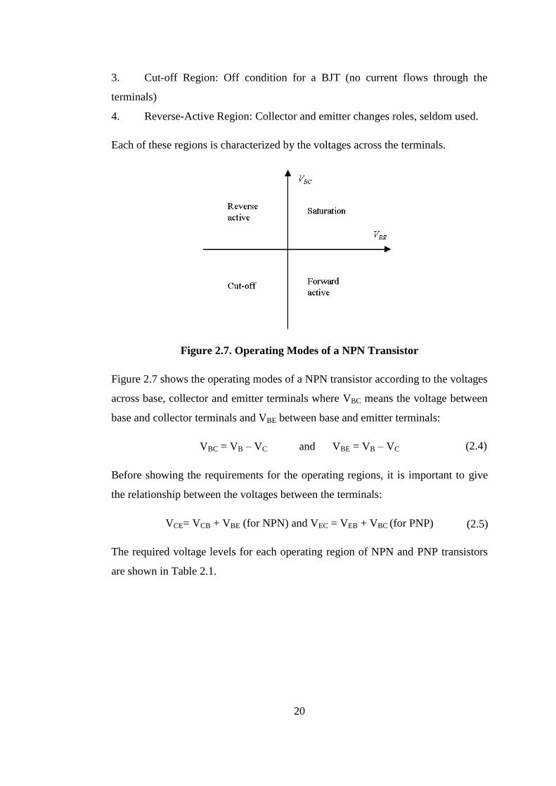
Each of these regions is characterized by the voltages across the terminals.
Figure 2.7. Operating Modes of a NPN Transistor
Figure 2.7 shows the operating modes of a NPN transistor according to the voltages
across base, collector and emitter terminals where VBC means the voltage between
base and collector terminals and VBE between base and emitter terminals:
VBC = VB – VC and VBE = VB – VC
Before showing the requirements for the operating regions, it is important to give
the relationship between the voltages between the terminals:
VCE= VCB + VBE (for NPN) and VEC = VEB + VBC (for PNP)
The required voltage levels for each operating region of NPN and PNP transistors
are shown in Table 2.1.
(2.4)
(2.5)
21
Table 2.1. BJT Operating Regions and Voltage Requirements
Region For NPN For PNP
Forward
Active
VCE > VCE(sat),
VBE > VBE(on) and VBC < 0
VEC > VEC(sat), VEB > VEB(on)
and VCB < 0
Saturation VCE < VCE(sat), VBE > VBE(on)
and VBC > 0
VEC < VEC(sat), VEB > VEB(on)
and VCB > 0
Cut-off VBE < VBE(on) and VBC < 0 VEB < VEB(on) and VCB < 0
Reverse
Active VBE < VBE(on) and VBC > 0 VEB < VEB(on) and VCB > 0
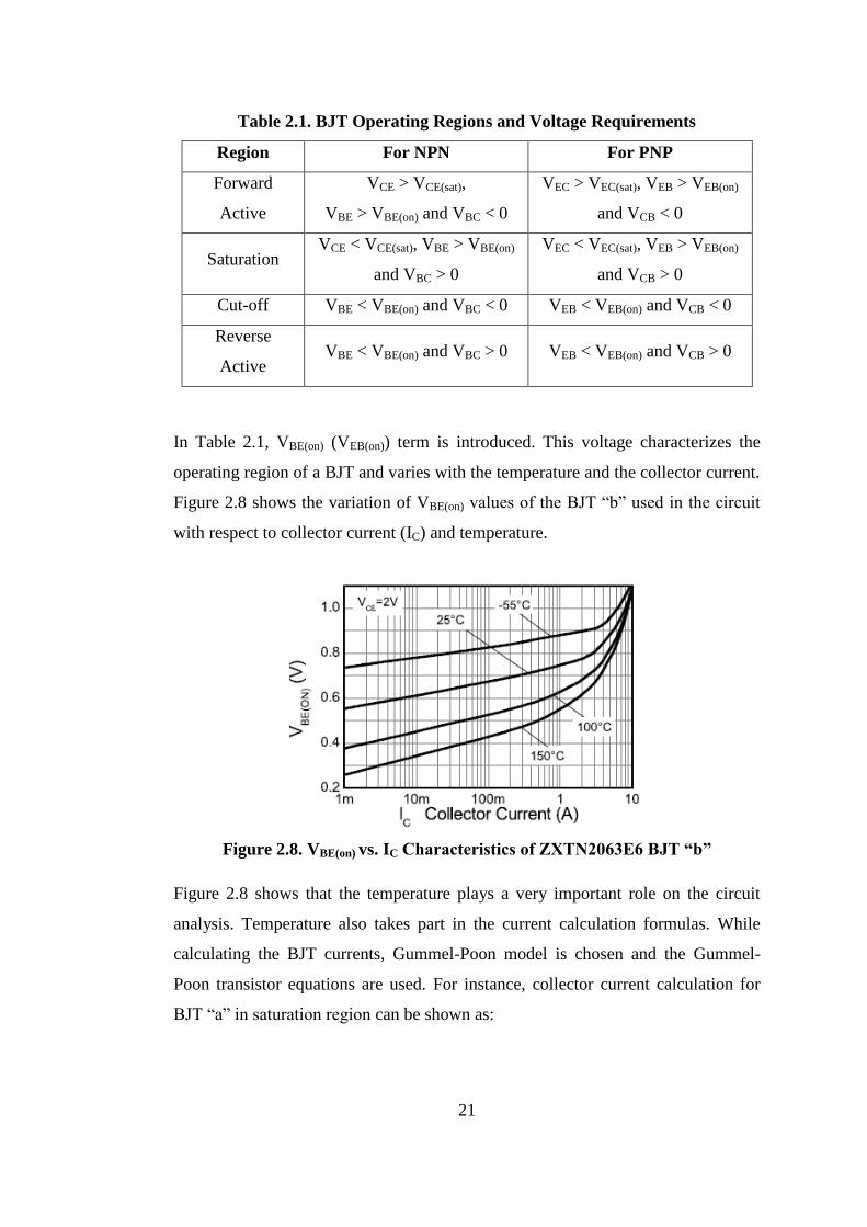
In Table 2.1, VBE(on) (VEB(on)) term is introduced. This voltage characterizes the
operating region of a BJT and varies with the temperature and the collector current.
Figure 2.8 shows the variation of VBE(on) values of the BJT “b” used in the circuit
with respect to collector current (IC) and temperature.
Figure 2.8. VBE(on) vs. IC Characteristics of ZXTN2063E6 BJT “b”
Figure 2.8 shows that the temperature plays a very important role on the circuit
analysis. Temperature also takes part in the current calculation formulas. While
calculating the BJT currents, Gummel-Poon model is chosen and the Gummel-
Poon transistor equations are used. For instance, collector current calculation for
BJT “a” in saturation region can be shown as:
22
It can be figured out from the formula that there are various parameters like Is, the
transport saturation current; Vt, the thermal voltage and βR, the ideal maximum
forward beta that effect the current values of a BJT. Details of the Gummel-Poon
model and the complete set of current equations can be reached from [1].
In the circuit scheme supplied in Figure 2.1, there are two BJT‟s, one NPN and one
PNP. In the circuit operation, these transistors are used as switches and their
normal region of operation must be Cut-off and Saturation respectively in order to
run the circuit properly. Throughout this study, PNP transistor in the circuit is
called as BJT “a” and the NPN transistor as BJT “b”.
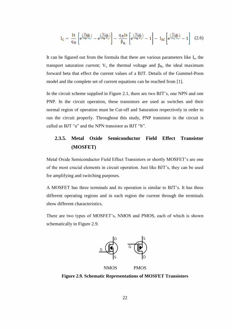
2.3.5. Metal Oxide Semiconductor Field Effect Transistor
(MOSFET)
Metal Oxide Semiconductor Field Effect Transistors or shortly MOSFET‟s are one
of the most crucial elements in circuit operation. Just like BJT‟s, they can be used
for amplifying and switching purposes.
A MOSFET has three terminals and its operation is similar to BJT‟s. It has three
different operating regions and in each region the current through the terminals
show different characteristics.
There are two types of MOSFET‟s, NMOS and PMOS, each of which is shown
schematically in Figure 2.9.
NMOS PMOS
Figure 2.9. Schematic Representations of MOSFET Transistors
(2.6)
23
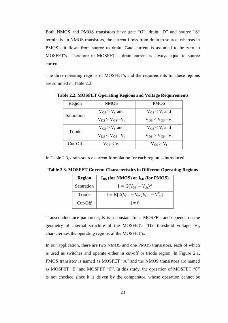
Both NMOS and PMOS transistors have gate “G”, drain “D” and source “S“
terminals. In NMOS transistors, the current flows from drain to source, whereas in
PMOS‟s it flows from source to drain. Gate current is assumed to be zero in
MOSFET‟s. Therefore in MOSFET‟s, drain current is always equal to source
current.
The three operating regions of MOSFET‟s and the requirements for these regions
are summed in Table 2.2.
Table 2.2. MOSFET Operating Regions and Voltage Requirements
Region NMOS PMOS
Saturation VGS > Vt and
VDS > VGS –Vt
VGS < Vt and
VDS < VGS –Vt
Triode VGS > Vt and
VDS < VGS –Vt
VGS < Vt and
VDS > VGS –Vt
Cut-Off VGS < Vt VGS > Vt
In Table 2.3, drain-source current formulation for each region is introduced.
Table 2.3. MOSFET Current Characteristics in Different Operating Regions
Region IDS (for NMOS) or ISD (for PMOS)
Saturation
Triode
Cut-Off I = 0
Transconductance parameter, K is a constant for a MOSFET and depends on the
geometry of internal structure of the MOSFET. The threshold voltage, Vth
characterizes the operating regions of the MOSFET‟s.
In our application, there are two NMOS and one PMOS transistors, each of which
is used as switches and operate either in cut-off or triode region. In Figure 2.1,
PMOS transistor is named as MOSFET “A” and the NMOS transistors are named
as MOSFET “B” and MOSFET “C”. In this study, the operation of MOSFET “C”
is not checked since it is driven by the comparator, whose operation cannot be
24
(2.7)
simulated with basic simulation tools. Thus, MOSFET “C” is assumed to be
operating properly since it only depends on the proper operation of the comparator.
Throughout this study, PMOS transistor is referred as MOSFET “A” and NMOS
transistor, whose operation is checked, as MOSFET “B”.
2.3.6. Comparator
A comparator is a basic integrated circuit which compares two voltage inputs and
generates an output voltage depending on the comparison of the input voltage. In
our circuit, one of the input nodes is connected to the reduced output voltage and
the other to 2.5V reference voltage. The reduced output voltage will be around the
reference voltage depending on the input voltage.
So what the comparator output will be:
5V if the reduced output voltage is higher than 2.5V
0V if the reduced output voltage is lower than 2.5V
A basic circuitry consisting of three resistors are used to reduce the output voltage
to voltages around 2.5V.
2.4. Circuit Analysis
In order to perform performance analysis for the circuit given in Figure 1, a set of
equations is generated utilizing the characteristics of each circuit element explained
above. However, the characteristics of the elements are not sufficient to build up all
the equations. Two basic principles are taken into consideration in the circuit
analysis: Kirchhoff‟s Voltage Law and Kirchhoff‟s Current Law. These two laws
are briefly explained next.
2.4.1. Kirchhoff’s Voltage Law (KVL)
KVL basically implies that the sum of all voltages around any closed circuit (loop)
equals zero. It can be formulated as
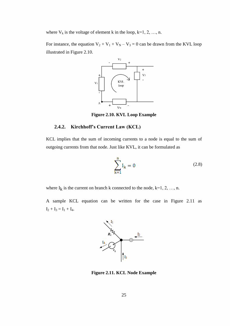
25
where Vk is the voltage of element k in the loop, k=1, 2, …, n.
For instance, the equation V2 + V1 + VN – V3 = 0 can be drawn from the KVL loop
illustrated in Figure 2.10.
Figure 2.10. KVL Loop Example
2.4.2. Kirchhoff’s Current Law (KCL)
KCL implies that the sum of incoming currents to a node is equal to the sum of
outgoing currents from that node. Just like KVL, it can be formulated as
where Ik is the current on branch k connected to the node, k=1, 2, …, n.
A sample KCL equation can be written for the case in Figure 2.11 as
I2 + I3 = I1 + I4.
Figure 2.11. KCL Node Example
(2.8)
26
CHAPTER 3
PROBLEM DEFINITION
Monte Carlo simulation is widely used in reliability analysis of complicated
electronic circuits ([2],[4],[8],[11],[12]). Given the tolerance bands of the elements
in the circuit, simulation produces the possible realizations of the circuit
performance. However, this simulation can only provide limited worst case results.
The main purpose of this study is to perform reliability analysis of the fuel pump
driver circuit ensuring the real worst case conditions. The worst case results are
obtained by solving linear and nonlinear circuit equations taking into consideration
the tolerance bands of resistances and temperature interval.
Unlike most of the worst case circuit analysis studies in the literature, temperature
effect is also taken into account by defining it as a decision variable varying in the
operating temperature interval of the circuit. This helps us to see the circuit‟s
performance in harsh environments.
There are various issues in reliability analysis. In this work we perform the
following two analyses:
1) Worst case circuit tolerance analysis at discrete power output requirements
2) Failure modes and effect analysis
Before starting with the analysis, the fuel pump driver circuit‟s normal operation
will be explained.
27
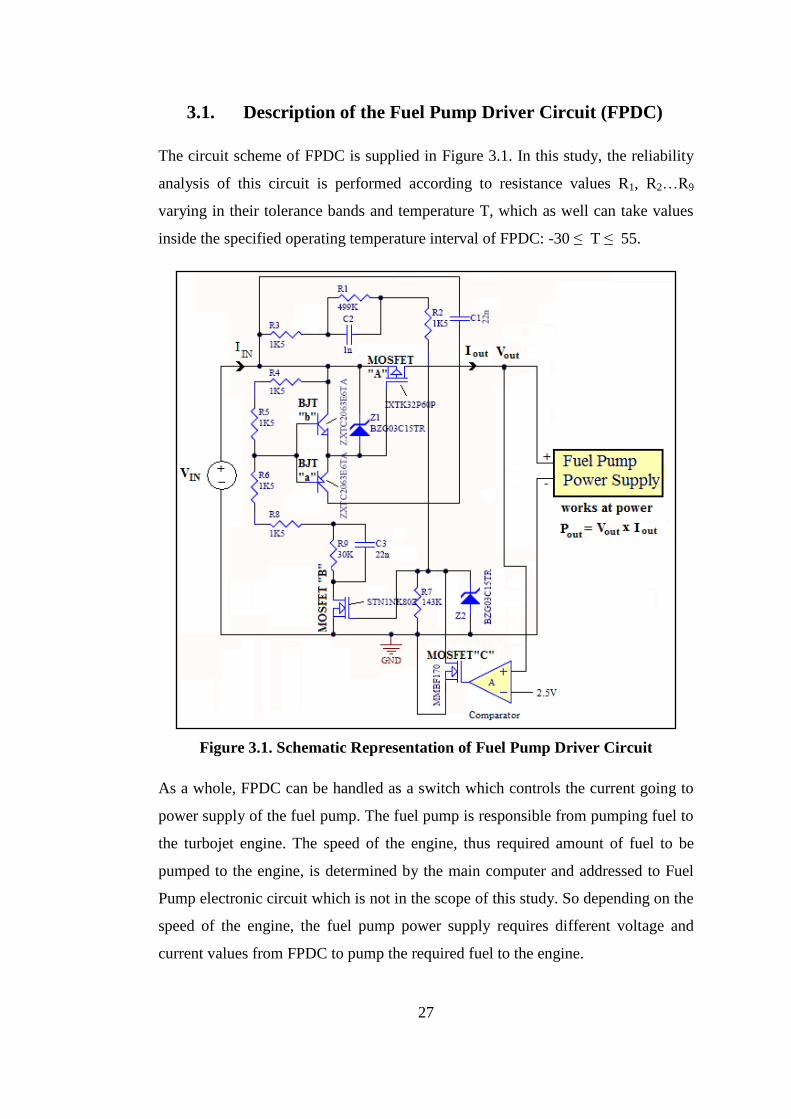
3.1. Description of the Fuel Pump Driver Circuit (FPDC)
The circuit scheme of FPDC is supplied in Figure 3.1. In this study, the reliability
analysis of this circuit is performed according to resistance values R1, R2…R9
varying in their tolerance bands and temperature T, which as well can take values
inside the specified operating temperature interval of FPDC: -30 ≤ T ≤ 55.
Figure 3.1. Schematic Representation of Fuel Pump Driver Circuit
As a whole, FPDC can be handled as a switch which controls the current going to
power supply of the fuel pump. The fuel pump is responsible from pumping fuel to
the turbojet engine. The speed of the engine, thus required amount of fuel to be
pumped to the engine, is determined by the main computer and addressed to Fuel
Pump electronic circuit which is not in the scope of this study. So depending on the
speed of the engine, the fuel pump power supply requires different voltage and
current values from FPDC to pump the required fuel to the engine.
28
The alternator which converts the mechanical energy of the engine to electrical
energy supplies voltage to FPDC. Faster the engine rotates the higher voltage the
alternator generates. Thus a linear relationship can be established between the
output power requirement and the input voltage of the pump driver circuit.
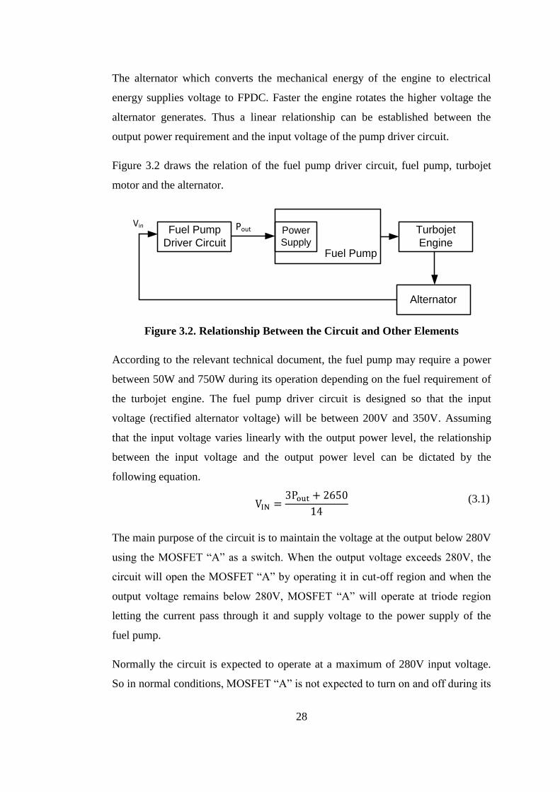
Figure 3.2 draws the relation of the fuel pump driver circuit, fuel pump, turbojet
motor and the alternator.
PoutFuel Pump
Driver Circuit
Power
SupplyFuel Pump
Turbojet
Engine
Alternator
Vin
Figure 3.2. Relationship Between the Circuit and Other Elements
According to the relevant technical document, the fuel pump may require a power
between 50W and 750W during its operation depending on the fuel requirement of
the turbojet engine. The fuel pump driver circuit is designed so that the input
voltage (rectified alternator voltage) will be between 200V and 350V. Assuming
that the input voltage varies linearly with the output power level, the relationship
between the input voltage and the output power level can be dictated by the
following equation.
The main purpose of the circuit is to maintain the voltage at the output below 280V
using the MOSFET “A” as a switch. When the output voltage exceeds 280V, the
circuit will open the MOSFET “A” by operating it in cut-off region and when the
output voltage remains below 280V, MOSFET “A” will operate at triode region
letting the current pass through it and supply voltage to the power supply of the
fuel pump.
Normally the circuit is expected to operate at a maximum of 280V input voltage.
So in normal conditions, MOSFET “A” is not expected to turn on and off during its
(3.1)
29
operation. In this study, assuming the input voltage will remain below 280V, the
operation of the circuit will be analyzed for tolerant resistance values and varying
temperature at discrete input voltages or output powers.
3.2. Problems Under Consideration
The problem considered here serves purpose for analyzing the circuit operation by
checking the transistor voltage levels. In this problem, the control/decision
variables are resistance values R1, R2…R9, temperature T and the voltage input
VIN. The rest of the variables (voltage, current levels etc..) are determined by these
control variables. Their values are uniquely determined according to T and VIN
values at the instance. Note that R1, R2…R9 vary within their tolerance bands
which is ±5% in our case and T can take any value between -30 and 55 °C.
In the real case, neither tolerant resistance values, nor the temperature and the
voltage input values can be controlled. However, they are treated as control
variables in the optimization routine. The optimizations are performed in discrete
VIN instances, while R1, R2…R9 and T variables are iteratively generated by
ModeFrontier program and sent to MATLAB, where the problem is defined and
the equations are solved for the instant R1, R2…R9 and T values.
By solving the problem defined here, it is intended to observe:
1) The effect of the resistor tolerances which arises from manufacturing
process and cannot be controlled.
2) To verify that the circuit operates properly in the specified operating
temperature of the circuit.
3) To make sure that the circuit operates properly in 200 ≤ VIN ≤ 280 interval.
The problem is handled by solving several non-linear programs. The objective
function will be changed sequentially to check the condition at certain nodes of the
circuit while all of the constraints governing the system are satisfied.
In this section, the description of the variables, constants, constraints and the
objectives with their check conditions are provided. Firstly, the decision variables
30
and the constants that are used in the problem will be introduced. There are 44
variables including the decision variables and the uncontrollable variables. Table
3.1 lists the uncontrollable variables and their descriptions.
Table 3.1. Descriptions of Uncontrollable Variables
Decision Variable Description
I1 Current through R3
I2 Current through R4
I3 Current through R7
Iz1 Reverse Current through Z1
Iz2 Reverse Current through Z2
ICa Collector Current of BJT “a”
IEa Emitter Current of BJT “a”
IBa Base Current of BJT “a”
ICb Collector Current of BJT “b”
IEb Emitter Current of BJT “b”
IBb Base Current of BJT “b”
ISDA Current through MOSFET “A”
IDSB Current through MOSFET “B”
IIN Input Current
VDSB Drain-to-Source Voltage of MOSFET “B”
VGSB Gate-to-Source Voltage of MOSFET “B”
VDSA Drain-to-Source Voltage of MOSFET “A”
VGSA Gate-to-Source Voltage of MOSFET “A”
VEca Emitter-to-Collector Voltage of BJT “a”
VEba Emitter-to-Base Voltage of BJT “a”
VBca Base-to-Collector Voltage of BJT “a”
VCeb Collector-to-Emitter Voltage of BJT “b”
VBeb Base-to-Emitter Voltage of BJT “b”
VCBb Collector-to-Base Voltage of BJT “b”
31
Table 3.1 (cont’d)
VC1 Voltage Across the C1
Vout Voltage at the Output
Vz1 Reverse Voltage Across Z1
Vz2 Reverse Voltage Across Z2
Vt Thermal Voltage
qBa Normalized majority base charge of BJT “a”
q1sa Variable used in Normalized majority base
charge calculation of BJT “a”
q2sa Variable used in Normalized majority base
charge calculation of BJT “a”
Pout Output Power
Emitter-Base Turn-On Voltage of BJT “a”
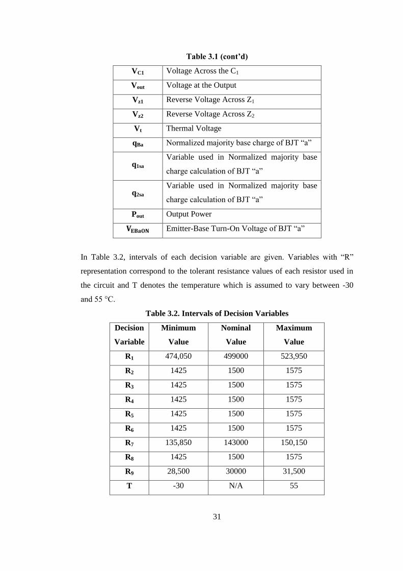
In Table 3.2, intervals of each decision variable are given. Variables with “R”
representation correspond to the tolerant resistance values of each resistor used in
the circuit and T denotes the temperature which is assumed to vary between -30
and 55 °C.
Table 3.2. Intervals of Decision Variables
Decision
Variable
Minimum
Value
Nominal
Value
Maximum
Value
R1 474,050 499000 523,950
R2 1425 1500 1575
R3 1425 1500 1575
R4 1425 1500 1575
R5 1425 1500 1575
R6 1425 1500 1575
R7 135,850 143000 150,150
R8 1425 1500 1575
R9 28,500 30000 31,500
T -30 N/A 55
32
Note that each resistance value varies 5% around its nominal value. This 5%
tolerance arises from the manufacturing process and it is remarked at the technical
specification of every resistor.
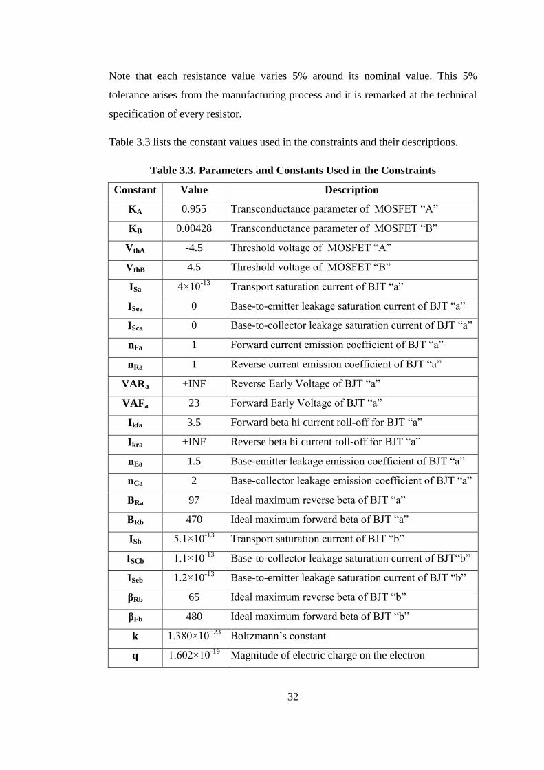
Table 3.3 lists the constant values used in the constraints and their descriptions.
Table 3.3. Parameters and Constants Used in the Constraints
Constant Value Description
KA 0.955 Transconductance parameter of MOSFET “A”
KB 0.00428 Transconductance parameter of MOSFET “B”
VthA -4.5 Threshold voltage of MOSFET “A”
VthB 4.5 Threshold voltage of MOSFET “B”
ISa 4×10-13
Transport saturation current of BJT “a”
ISea 0 Base-to-emitter leakage saturation current of BJT “a”
ISca 0 Base-to-collector leakage saturation current of BJT “a”
nFa 1 Forward current emission coefficient of BJT “a”
nRa 1 Reverse current emission coefficient of BJT “a”
VARa +INF Reverse Early Voltage of BJT “a”
VAFa 23 Forward Early Voltage of BJT “a”
Ikfa 3.5 Forward beta hi current roll-off for BJT “a”
Ikra +INF Reverse beta hi current roll-off for BJT “a”
nEa 1.5 Base-emitter leakage emission coefficient of BJT “a”
nCa 2 Base-collector leakage emission coefficient of BJT “a”
ΒRa 97 Ideal maximum reverse beta of BJT “a”
ΒRb 470 Ideal maximum forward beta of BJT “a”
ISb 5.1×10⁻¹³
Transport saturation current of BJT “b”
ISCb 1.1×10⁻¹³
Base-to-collector leakage saturation current of BJT“b”
ISeb 1.2×10⁻¹³
Base-to-emitter leakage saturation current of BJT “b”
βRb 65 Ideal maximum reverse beta of BJT “b”
βFb 480 Ideal maximum forward beta of BJT “b”
k 1.380×10⁻²³
Boltzmann‟s constant
q 1.602×10⁻¹⁹
Magnitude of electric charge on the electron
33
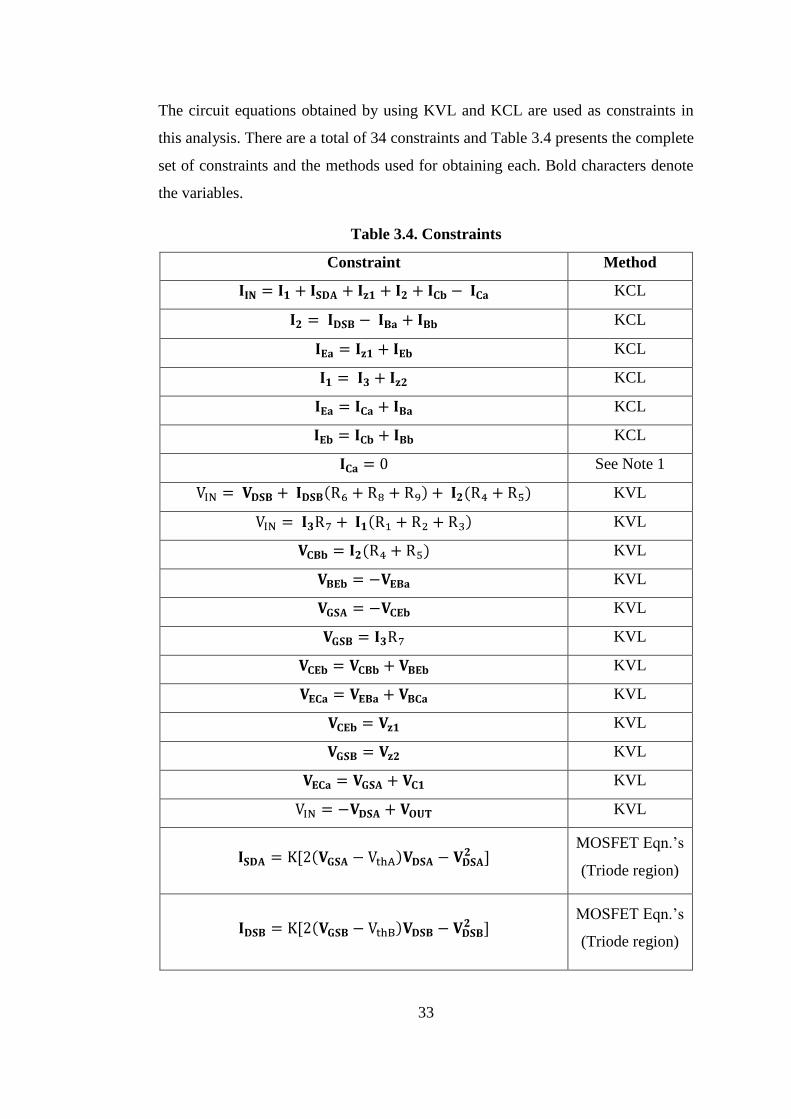
The circuit equations obtained by using KVL and KCL are used as constraints in
this analysis. There are a total of 34 constraints and Table 3.4 presents the complete
set of constraints and the methods used for obtaining each. Bold characters denote
the variables.
Table 3.4. Constraints
Constraint Method
KCL
KCL
KCL
KCL
KCL
KCL
See Note 1
KVL
KVL
KVL
KVL
KVL
KVL
KVL
KVL
KVL
KVL
KVL
KVL
MOSFET Eqn.‟s
(Triode region)
MOSFET Eqn.‟s
(Triode region)
34
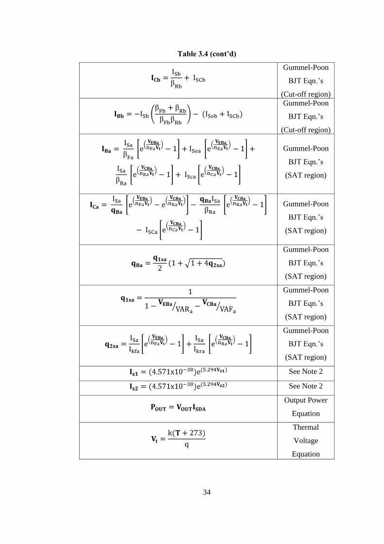
Table 3.4 (cont’d)
Gummel-Poon
BJT Eqn.‟s
(Cut-off region)
Gummel-Poon
BJT Eqn.‟s
(Cut-off region)
Gummel-Poon
BJT Eqn.‟s
(SAT region)
Gummel-Poon
BJT Eqn.‟s
(SAT region)
Gummel-Poon
BJT Eqn.‟s
(SAT region)
Gummel-Poon
BJT Eqn.‟s
(SAT region)
Gummel-Poon
BJT Eqn.‟s
(SAT region)
See Note 2
See Note 2
Output Power
Equation
Thermal
Voltage
Equation
35
Table 3.4 (cont’d)
Vin – Pout
Relationship
See Note 3
474,050 ≤ R1 ≤ 523,950 R1 tolerance
1425 ≤ R2 ≤ 1575 R2 tolerance
1425 ≤ R3 ≤ 1575 R3 tolerance
1425 ≤ R4 ≤ 1575 R4 tolerance
1425 ≤ R5 ≤ 1575 R5 tolerance
1425 ≤ R6 ≤ 1575 R6 tolerance
135,850 ≤ R7 ≤ 150,150 R7 tolerance
1425 ≤ R8 ≤ 1575 R8 tolerance
28,500 ≤ R9 ≤ 31,500 R9 tolerance
-30 ≤ T ≤ 55 Temperature
interval
Note 1: It is known that . Since the circuit is
analyzed at steady state conditions and at no voltage variations, we can say that VC1
does not vary with time. Therefore we can conclude that as shown
in the table.
Note 2: Actually in the literature no relationship has been established between
reverse voltage (Vz) and reverse current (Iz) of zener diodes. What we have done
here to relate them is to use the simulation results of the zener diode with part
number BZG03C15TR which is used in the design and fit the simulation
characteristics into an equation.
Note 3: There is no formulized relationship between VBEaON, ICa and T in the
literature as well. The data points in Figure 3.3 which represents VBEaON vs. ICa
relationship of BJT “a” at various temperatures are used to relate VBEaON and T.
36
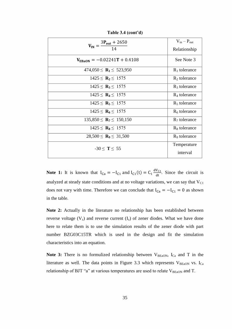
Figure 3.3. VBEaON vs. ICa Characteristics [17]
Noting that , the relationship between VEBaON and T has been
formed using the data points in the leftmost part of the graph (the points with the
smallest values).
3.3. Objectives
There are 8 linear objectives each of which will be optimized separately. The
objectives are chosen in order to check the circuit‟s operation in different
temperature and resistance values.
The transistors in FPDC behave like switches such that the circuit operates properly
only if each transistor stays in its correct position. So it is vital to check all the
MOSFET and BJT voltages if they remain in the range that obeys the assumed
operation regions. Table 3.5 shows the region each transistor is assumed to operate
in and the conditions for those regions.
Table 3.5. Assumed Transistor Operating Regions and Required Conditions
Transistor Operating Region Required Conditions
BJT “b” Cut-off AND
BJT “a” Saturation AND
MOSFET “A” Triode
MOSFET “B” Triode
37
Note that VEC < VECa(sat), which as well is a required condition for MOSFET “A” to
operate in saturation region, is missing in Table 3.5. This is because running
computational analysis for this objective is unnecessary since VECa is minorly
affected by R1, R2…R9 and T variations and the exact value of VECa(sat) cannot be
exactly determined. According to technical datasheet of BJT “a”, VECa(sat) value is
around 0.01 V and VECa is found to be 0.0003 ± 0.0001 V in any R, T and VIN
values. Thus, it is assumed that this condition is satisfied and no computational
analysis will be performed for VECa.
The objective function forms and their check conditions are listed in Table 3.6.
Table 3.6. Objective Functions and Check Conditions
Objective Function Check Condition
Minimize
Maximize
Maximize
Minimize
Maximize
Minimize )
Minimize
Maximize ( )
If at any temperature and resistance value, for instance, is below 0 or is
above VBEbON, it can be said that BJT “b” operates in wrong region and circuit fails
at that temperature and resistance value.
3.4. Solution Method
To solve the nonlinear optimization problems defined above, MATLAB (ver.
R2006a) and ModeFRONTIER (MF) (ver. 4.0) softwares are used.
Note that when the variables R and T are fixed, the system of equations in Table
3.4 has a unique solution. We observed that MATLAB can quickly give this unique
38
solution whereas the optimization problem takes a long time in MATLAB when R
and T variables change in tolerance limit. On the other hand, ModeFRONTIER can
optimize the defined objective in an impressively short time by generating smart R
and T values iteratively and solving the equations in MATLAB with the generated
values. Hence we decided to use them sequentially, making evaluations in
MATLAB and improvements in MF. The solution times for each problem vary
with the complexity of the relevant objective function. However, it can be said that
the maximum solution time in one VIN instance is reduced to 24 minutes with the
iterative use of MATLAB and MF.
Figure 3.4 shows the optimization flowchart of the problem. This optimization
routine is repeated for all the objectives defined in Table 3.6.
MATLAB solves the
equations and computes
the unique solution
Initial
VIN=200
MF generates
R1..R9 and T
values to improve
the objective
R1R2 ... R9 T
Vin=
280 ?
VIN = VIN +4
Obj.
Impr. ≤ 1e-5
?
Yes
No
Solution
No
END
Yes
Figure 3.4. Optimization Flowchart
MATLAB is used for defining all the constant values and the constraints. Decision
variables, T and R1, R2…R9 are also defined as constants in MATLAB code.
However the values of these variables are generated from MF.
The objective functions are described in MF and the software runs a pre-defined
algorithm for optimization. In this study, each objective is optimized for
21 different power output (Pout) requirements and the optimum values in different
requirements are graphically illustrated below.
39
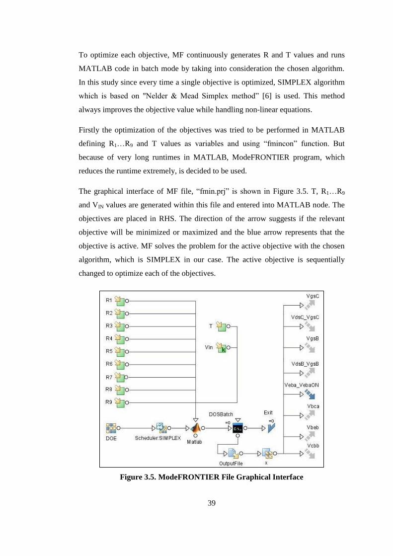
To optimize each objective, MF continuously generates R and T values and runs
MATLAB code in batch mode by taking into consideration the chosen algorithm.
In this study since every time a single objective is optimized, SIMPLEX algorithm
which is based on "Nelder & Mead Simplex method” [6] is used. This method
always improves the objective value while handling non-linear equations.
Firstly the optimization of the objectives was tried to be performed in MATLAB
defining R1…R9 and T values as variables and using “fmincon” function. But
because of very long runtimes in MATLAB, ModeFRONTIER program, which
reduces the runtime extremely, is decided to be used.
The graphical interface of MF file, “fmin.prj” is shown in Figure 3.5. T, R1…R9
and VIN values are generated within this file and entered into MATLAB node. The
objectives are placed in RHS. The direction of the arrow suggests if the relevant
objective will be minimized or maximized and the blue arrow represents that the
objective is active. MF solves the problem for the active objective with the chosen
algorithm, which is SIMPLEX in our case. The active objective is sequentially
changed to optimize each of the objectives.
Figure 3.5. ModeFRONTIER File Graphical Interface
40
CHAPTER 4
WORST CASE CIRCUIT TOLERANCE ANALYSIS
In this chapter, circuit performance is examined under varying temperature and
resistance values. The following sections include the optimization results of the
problems defined in CHAPTER 3. The optimum values achieved for each of the
objectives represent the worst case conditions for the circuit operation. In this way,
it is aimed to observe that the circuit operates properly even in the worst case
conditions.
4.1. Optimization Results
This section includes the results obtained by MATLAB and ModeFRONTIER
softwares. The optimum values of the objectives shown in Table 3.6 are
respectively supplied for the required range 50 Pout 420 watts in figures and the
binding tolerance constraints for each objective are given.
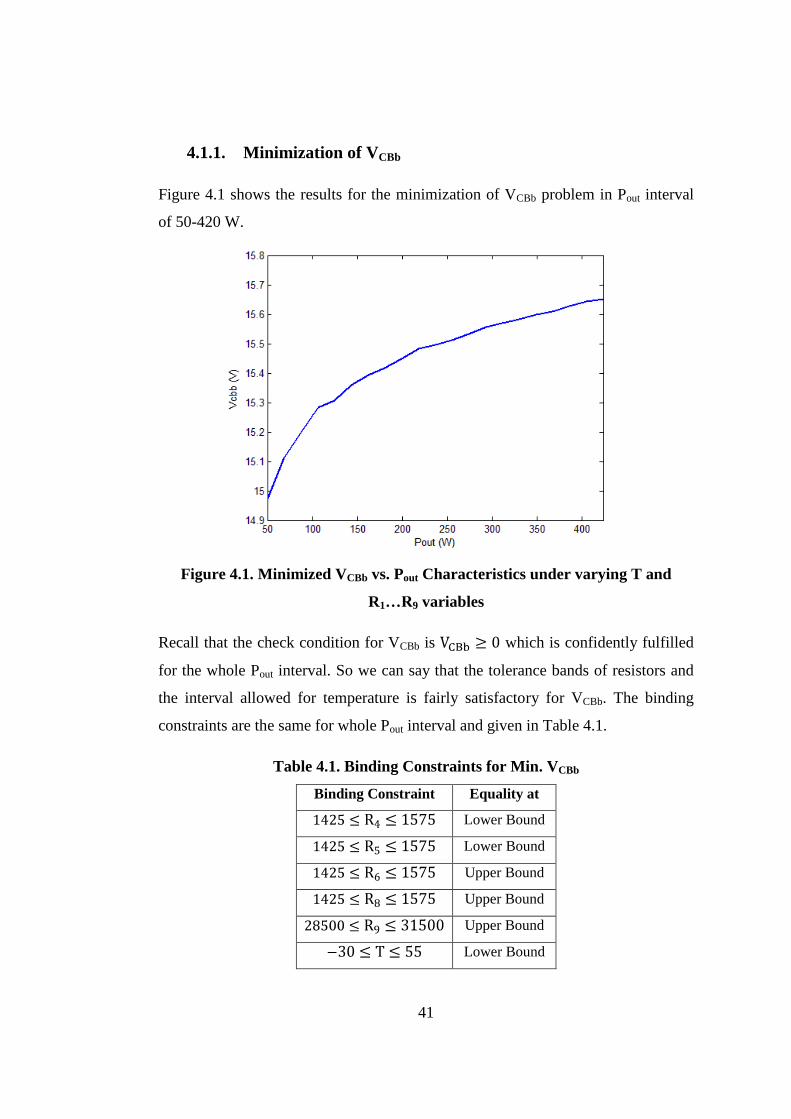
41
4.1.1. Minimization of VCBb
Figure 4.1 shows the results for the minimization of VCBb problem in Pout interval
of 50-420 W.
Figure 4.1. Minimized VCBb vs. Pout Characteristics under varying T and
R1…R9 variables
Recall that the check condition for VCBb is which is confidently fulfilled
for the whole Pout interval. So we can say that the tolerance bands of resistors and
the interval allowed for temperature is fairly satisfactory for VCBb. The binding
constraints are the same for whole Pout interval and given in Table 4.1.
Table 4.1. Binding Constraints for Min. VCBb
Binding Constraint Equality at
Lower Bound
Lower Bound
Upper Bound
Upper Bound
Upper Bound
Lower Bound
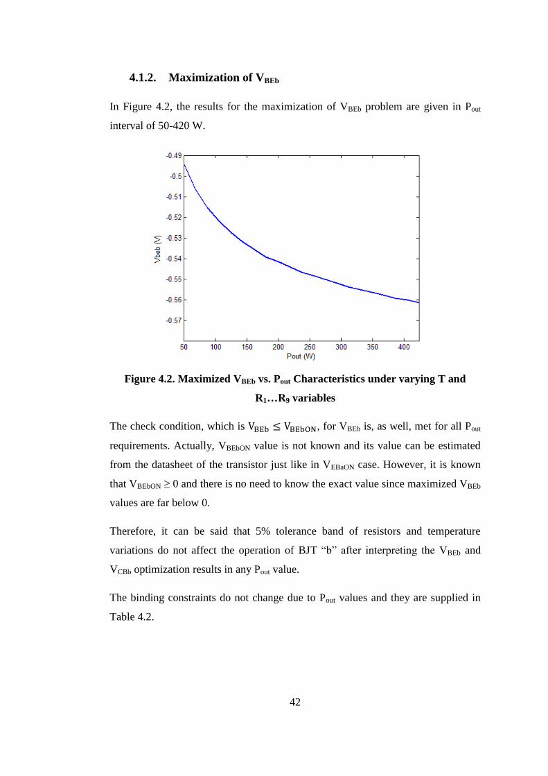
42
4.1.2. Maximization of VBEb
In Figure 4.2, the results for the maximization of VBEb problem are given in Pout
interval of 50-420 W.
Figure 4.2. Maximized VBEb vs. Pout Characteristics under varying T and
R1…R9 variables
The check condition, which is , for VBEb is, as well, met for all Pout
requirements. Actually, VBEbON value is not known and its value can be estimated
from the datasheet of the transistor just like in VEBaON case. However, it is known
that VBEbON ≥ 0 and there is no need to know the exact value since maximized VBEb
values are far below 0.
Therefore, it can be said that 5% tolerance band of resistors and temperature
variations do not affect the operation of BJT “b” after interpreting the VBEb and
VCBb optimization results in any Pout value.
The binding constraints do not change due to Pout values and they are supplied in
Table 4.2.
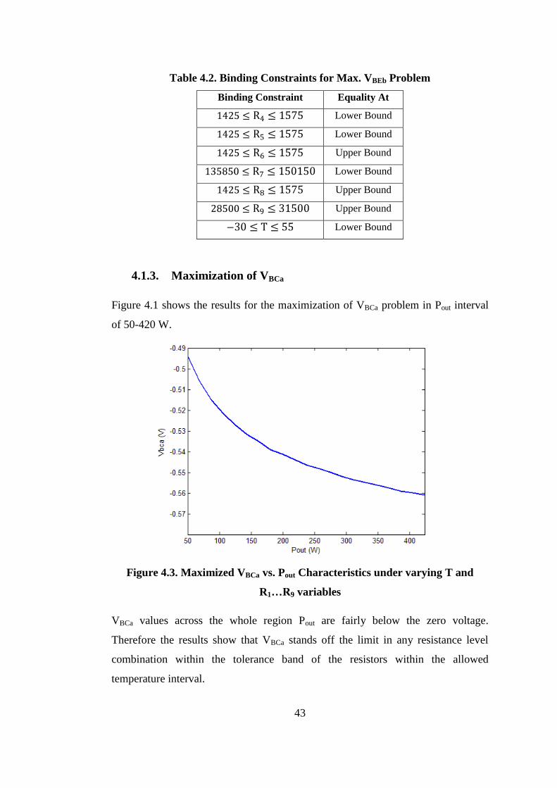
43
Table 4.2. Binding Constraints for Max. VBEb Problem
Binding Constraint Equality At
Lower Bound
Lower Bound
Upper Bound
Lower Bound
Upper Bound
Upper Bound
Lower Bound
4.1.3. Maximization of VBCa
Figure 4.1 shows the results for the maximization of VBCa problem in Pout interval
of 50-420 W.
Figure 4.3. Maximized VBCa vs. Pout Characteristics under varying T and
R1…R9 variables
VBCa values across the whole region Pout are fairly below the zero voltage.
Therefore the results show that VBCa stands off the limit in any resistance level
combination within the tolerance band of the resistors within the allowed
temperature interval.
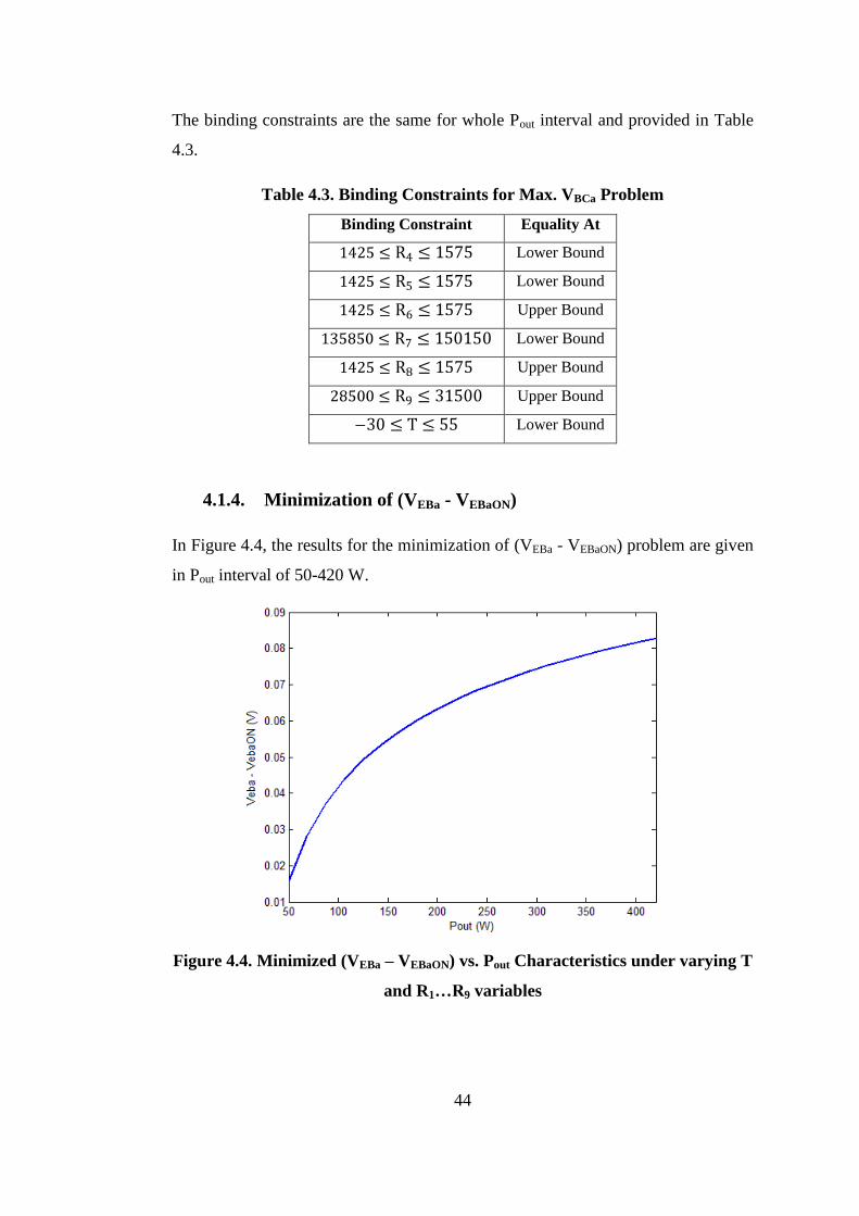
44
The binding constraints are the same for whole Pout interval and provided in Table
4.3.
Table 4.3. Binding Constraints for Max. VBCa Problem
Binding Constraint Equality At
Lower Bound
Lower Bound
Upper Bound
Lower Bound
Upper Bound
Upper Bound
Lower Bound
4.1.4. Minimization of (VEBa - VEBaON)
In Figure 4.4, the results for the minimization of (VEBa - VEBaON) problem are given
in Pout interval of 50-420 W.
Figure 4.4. Minimized (VEBa – VEBaON) vs. Pout Characteristics under varying T
and R1…R9 variables
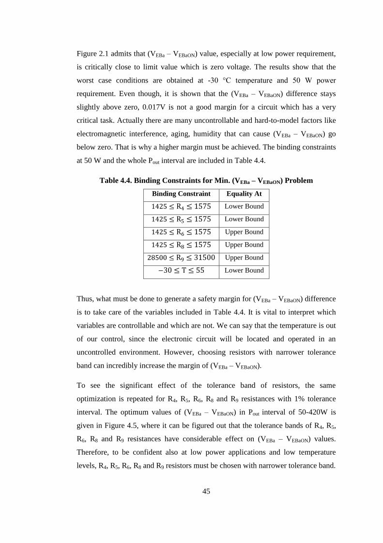
45
Figure 2.1 admits that (VEBa – VEBaON) value, especially at low power requirement,
is critically close to limit value which is zero voltage. The results show that the
worst case conditions are obtained at -30 °C temperature and 50 W power
requirement. Even though, it is shown that the (VEBa – VEBaON) difference stays
slightly above zero, 0.017V is not a good margin for a circuit which has a very
critical task. Actually there are many uncontrollable and hard-to-model factors like
electromagnetic interference, aging, humidity that can cause (VEBa – VEBaON) go
below zero. That is why a higher margin must be achieved. The binding constraints
at 50 W and the whole Pout interval are included in Table 4.4.
Table 4.4. Binding Constraints for Min. (VEBa – VEBaON) Problem
Binding Constraint Equality At
Lower Bound
Lower Bound
Upper Bound
Upper Bound
Upper Bound
Lower Bound
Thus, what must be done to generate a safety margin for (VEBa – VEBaON) difference
is to take care of the variables included in Table 4.4. It is vital to interpret which
variables are controllable and which are not. We can say that the temperature is out
of our control, since the electronic circuit will be located and operated in an
uncontrolled environment. However, choosing resistors with narrower tolerance
band can incredibly increase the margin of (VEBa – VEBaON).
To see the significant effect of the tolerance band of resistors, the same
optimization is repeated for R4, R5, R6, R8 and R9 resistances with 1% tolerance
interval. The optimum values of (VEBa – VEBaON) in Pout interval of 50-420W is
given in Figure 4.5, where it can be figured out that the tolerance bands of R4, R5,
R6, R8 and R9 resistances have considerable effect on (VEBa – VEBaON) values.
Therefore, to be confident also at low power applications and low temperature
levels, R4, R5, R6, R8 and R9 resistors must be chosen with narrower tolerance band.
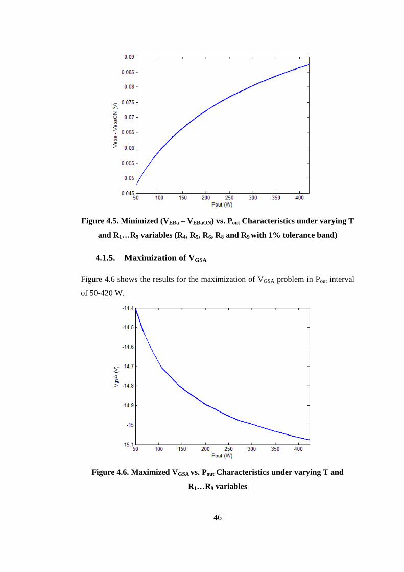
46
Figure 4.5. Minimized (VEBa – VEBaON) vs. Pout Characteristics under varying T
and R1…R9 variables (R4, R5, R6, R8 and R9 with 1% tolerance band)
4.1.5. Maximization of VGSA
Figure 4.6 shows the results for the maximization of VGSA problem in Pout interval
of 50-420 W.
Figure 4.6. Maximized VGSA vs. Pout Characteristics under varying T and
R1…R9 variables
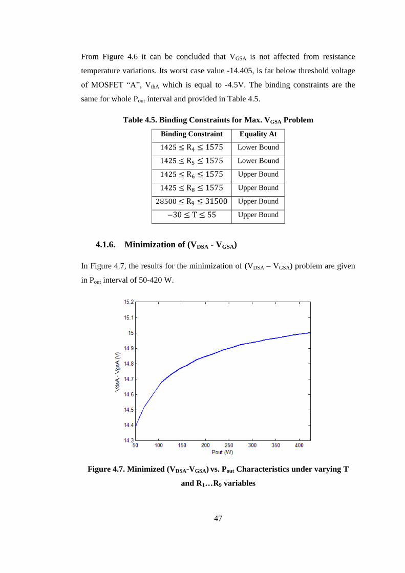
47
From Figure 4.6 it can be concluded that VGSA is not affected from resistance
temperature variations. Its worst case value -14.405, is far below threshold voltage
of MOSFET “A”, VthA which is equal to -4.5V. The binding constraints are the
same for whole Pout interval and provided in Table 4.5.
Table 4.5. Binding Constraints for Max. VGSA Problem
Binding Constraint Equality At
Lower Bound
Lower Bound
Upper Bound
Upper Bound
Upper Bound
Upper Bound
4.1.6. Minimization of (VDSA - VGSA)
In Figure 4.7, the results for the minimization of (VDSA – VGSA) problem are given
in Pout interval of 50-420 W.
Figure 4.7. Minimized (VDSA-VGSA) vs. Pout Characteristics under varying T
and R1…R9 variables
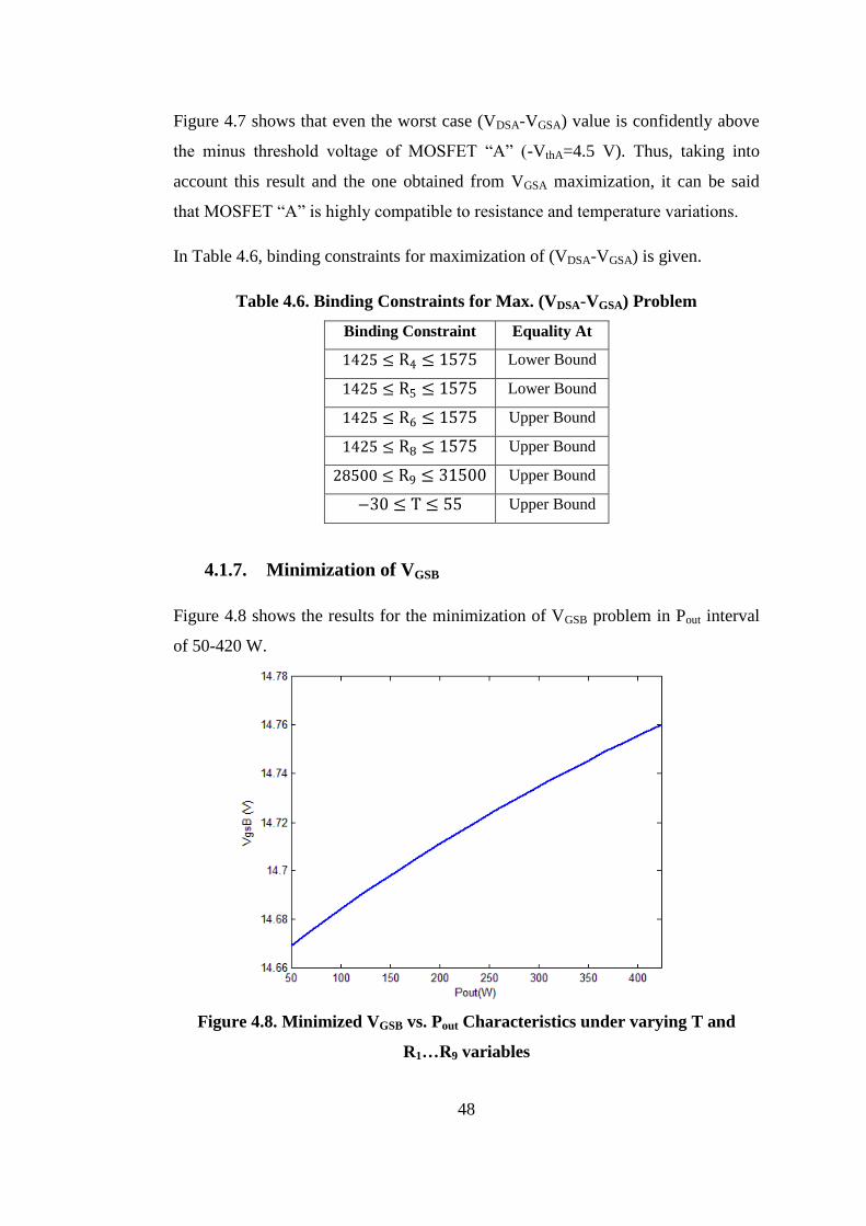
48
Figure 4.7 shows that even the worst case (VDSA-VGSA) value is confidently above
the minus threshold voltage of MOSFET “A” (-VthA=4.5 V). Thus, taking into
account this result and the one obtained from VGSA maximization, it can be said
that MOSFET “A” is highly compatible to resistance and temperature variations.
In Table 4.6, binding constraints for maximization of (VDSA-VGSA) is given.
Table 4.6. Binding Constraints for Max. (VDSA-VGSA) Problem
Binding Constraint Equality At
Lower Bound
Lower Bound
Upper Bound
Upper Bound
Upper Bound
Upper Bound
4.1.7. Minimization of VGSB
Figure 4.8 shows the results for the minimization of VGSB problem in Pout interval
of 50-420 W.
Figure 4.8. Minimized VGSB vs. Pout Characteristics under varying T and
R1…R9 variables
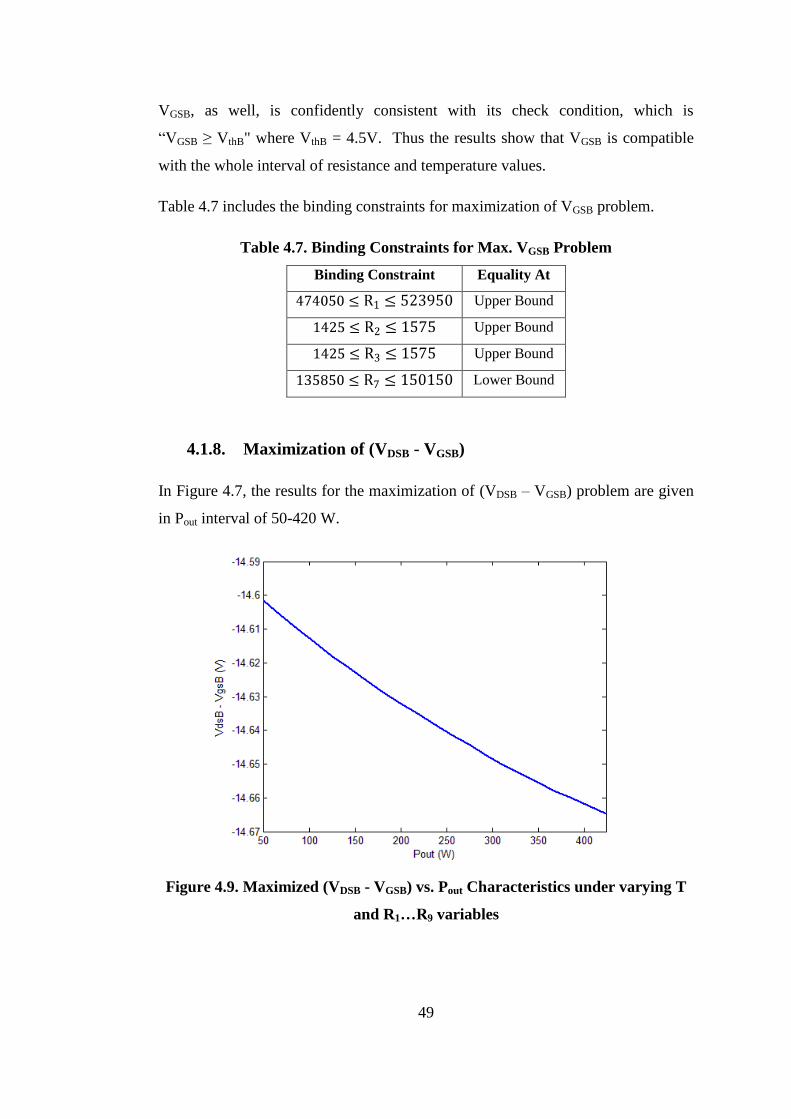
49
VGSB, as well, is confidently consistent with its check condition, which is
“VGSB ≥ VthB" where VthB = 4.5V. Thus the results show that VGSB is compatible
with the whole interval of resistance and temperature values.
Table 4.7 includes the binding constraints for maximization of VGSB problem.
Table 4.7. Binding Constraints for Max. VGSB Problem
Binding Constraint Equality At
Upper Bound
Upper Bound
Upper Bound
Lower Bound
4.1.8. Maximization of (VDSB - VGSB)
In Figure 4.7, the results for the maximization of (VDSB – VGSB) problem are given
in Pout interval of 50-420 W.
Figure 4.9. Maximized (VDSB - VGSB) vs. Pout Characteristics under varying T
and R1…R9 variables
50
Figure 4.9 indicates that (VDSB - VGSB) objective also holds its check condition
(VDSB - VGSB) ≤ -VthB. Therefore, taking into consideration the optimization results
of VGSB and (VDSB - VGSB), it can be concluded that MOSFET “B” operates in the
right region within the tolerance band of resistors and the temperature variations.
The binding constraints for maximization of (VDSB - VGSB) are included in Table
4.8.
Table 4.8. Binding Constraints for Max. VGSB Problem
Binding Constraint Equality At
Upper Bound
Upper Bound
Upper Bound
Lower Bound
Lower Bound
Lower Bound
Lower Bound
4.2. Interpretation of Optimization Results
The optimization results show that under varying T and R1…R9 variables all the
check conditions hold in any Pout value in the interval of 50-420 watts. While some
objectives like (VEBa - VEBaON) are slightly above or below their limit, some are
confidently consistent with their check conditions.
When dealing with the results component by component, it can be said that BJT
“a” has the most critical condition, by means of its (VEBa - VEBaON) voltage. To
apply a meaningful safety margin for that voltage level, R4, R5, R6, R8 and R9
resistors must be replaced with their identical parts with 1% tolerance band.
The voltage levels of BJT “b”, MOSFET “A” and MOSFET “B” have enough
safety margin from their critical value, thus we can conclude that these components
are highly compatible to temperature variations between -30°C / 55°C and 5%
tolerance band of the resistors.
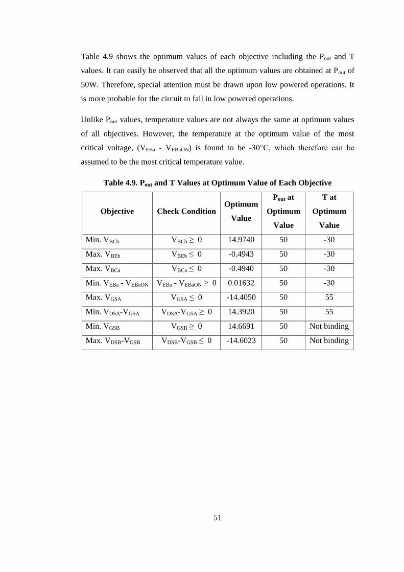
51
Table 4.9 shows the optimum values of each objective including the Pout and T
values. It can easily be observed that all the optimum values are obtained at Pout of
50W. Therefore, special attention must be drawn upon low powered operations. It
is more probable for the circuit to fail in low powered operations.
Unlike Pout values, temperature values are not always the same at optimum values
of all objectives. However, the temperature at the optimum value of the most
critical voltage, (VEBa - VEBaON) is found to be -30°C, which therefore can be
assumed to be the most critical temperature value.
Table 4.9. Pout and T Values at Optimum Value of Each Objective
Objective Check Condition Optimum
Value
Pout at
Optimum
Value
T at
Optimum
Value
Min. VBCb VBCb ≥ 0 14.9740 50 -30
Max. VBEb VBEb ≤ 0 -0.4943 50 -30
Max. VBCa VBCa ≤ 0 -0.4940 50 -30
Min. VEBa - VEBaON VEBa - VEBaON ≥ 0 0.01632 50 -30
Max. VGSA VGSA ≤ 0 -14.4050 50 55
Min. VDSA-VGSA VDSA-VGSA ≥ 0 14.3920 50 55
Min. VGSB VGSB ≥ 0 14.6691 50 Not binding
Max. VDSB-VGSB VDSB-VGSB ≤ 0 -14.6023 50 Not binding
52
CHAPTER 5
FAILURE MODES AND EFFECTS ANALYSIS
Each electronic component has a possibility of failing and the mechanisms of these
failures vary from component to component. Most common failures are short
circuit and open circuit failures which are the primary causes of the failures for
most of the components. Other failures cover drift, parameter change, intermittent
connection etc.. However, the failures which affect the circuit operation in the
worst manner are the short and open circuit failures.
In this study, the effects of open circuit and short circuit failures of all the
components in FPDC will be examined. Some failures do not affect the circuit
operation at all, while some may cause catastrophic circuit failure. To examine the
effects of each failure, tolerance analysis is carried out when necessary. Yet the
effects of some failures are so obvious that they can be figured out at a glance on
the circuit scheme. Thus; no further analyses are needed for the failures whose
effect can be obviously realized. In this study, only the failures whose effect cannot
be obviously figured out are handled.
In this section, primarily brief information about short circuit and open circuit
failures is given and then the effects of short and open circuit failures of each
component used in the circuit are analyzed.
53
5.1. Short Circuit Failure
When a component undergoes a short circuit failure, an extremely low resistance is
observed between its terminals and the component acts simply like a wire. So while
analyzing the short circuit failure of a component, whatever its type is, the
component will be bypassed with simple wire across its terminals. The effect of
this failure will be analyzed with MATLAB and ModeFRONTIER, when
necessary.
5.2. Open Circuit Failure
This failure causes an unexpected disconnection between the terminals of a
component. When an open circuit failure happens in a component, no current
passes through it and the path including the component acts like a cut wire.
This, as well, is a very important type of failure and can happen in most of the
components. While analyzing the open circuit failure, the current through the
relevant path is assumed to be zero and the effect of the failure will be again
examined with MATLAB and Mode FRONTIER over the whole region of VIN,
when necessary.
5.3. FMEA Matrix
There are a total number of 18 electronic components in FPDC. Investigating the
short circuit and open circuit failures of each component by MATLAB and
ModeFRONTIER softwares takes extremely long time. Hence, it is unnecessary to
perform the analysis for the failures whose effect is obvious and can be realized
without any computation.
In this section, a matrix which includes the failures of each component and their
effects is given. In this matrix, the failures that need a computational analysis are
also shown.
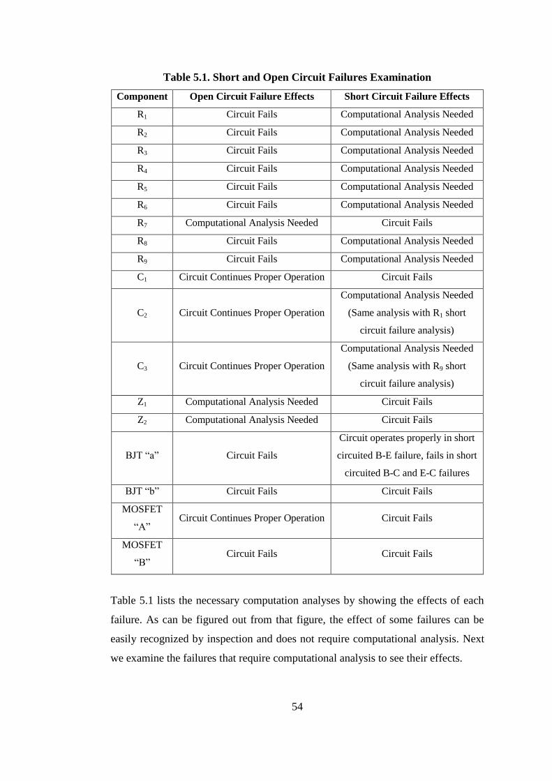
54
Table 5.1. Short and Open Circuit Failures Examination
Component Open Circuit Failure Effects Short Circuit Failure Effects
R1 Circuit Fails Computational Analysis Needed
R2 Circuit Fails Computational Analysis Needed
R3 Circuit Fails Computational Analysis Needed
R4 Circuit Fails Computational Analysis Needed
R5 Circuit Fails Computational Analysis Needed
R6 Circuit Fails Computational Analysis Needed
R7 Computational Analysis Needed Circuit Fails
R8 Circuit Fails Computational Analysis Needed
R9 Circuit Fails Computational Analysis Needed
C1 Circuit Continues Proper Operation Circuit Fails
C2 Circuit Continues Proper Operation
Computational Analysis Needed
(Same analysis with R1 short
circuit failure analysis)
C3 Circuit Continues Proper Operation
Computational Analysis Needed
(Same analysis with R9 short
circuit failure analysis)
Z1 Computational Analysis Needed Circuit Fails
Z2 Computational Analysis Needed Circuit Fails
BJT “a” Circuit Fails
Circuit operates properly in short
circuited B-E failure, fails in short
circuited B-C and E-C failures
BJT “b” Circuit Fails Circuit Fails
MOSFET
“A” Circuit Continues Proper Operation Circuit Fails
MOSFET
“B” Circuit Fails Circuit Fails
Table 5.1 lists the necessary computation analyses by showing the effects of each
failure. As can be figured out from that figure, the effect of some failures can be
easily recognized by inspection and does not require computational analysis. Next
we examine the failures that require computational analysis to see their effects.
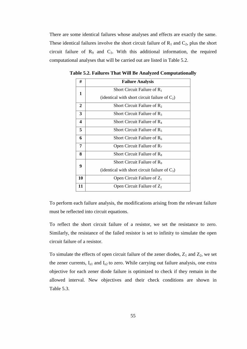
55
There are some identical failures whose analyses and effects are exactly the same.
These identical failures involve the short circuit failure of R1 and C2, plus the short
circuit failure of R9 and C3. With this additional information, the required
computational analyses that will be carried out are listed in Table 5.2.
Table 5.2. Failures That Will Be Analyzed Computationally
# Failure Analysis
1 Short Circuit Failure of R1
(identical with short circuit failure of C2)
2 Short Circuit Failure of R2
3 Short Circuit Failure of R3
4 Short Circuit Failure of R4
5 Short Circuit Failure of R5
6 Short Circuit Failure of R6
7 Open Circuit Failure of R7
8 Short Circuit Failure of R8
9 Short Circuit Failure of R9
(identical with short circuit failure of C3)
10 Open Circuit Failure of Z1
11 Open Circuit Failure of Z2
To perform each failure analysis, the modifications arising from the relevant failure
must be reflected into circuit equations.
To reflect the short circuit failure of a resistor, we set the resistance to zero.
Similarly, the resistance of the failed resistor is set to infinity to simulate the open
circuit failure of a resistor.
To simulate the effects of open circuit failure of the zener diodes, Z1 and Z2, we set
the zener currents, Iz1 and Iz2 to zero. While carrying out failure analysis, one extra
objective for each zener diode failure is optimized to check if they remain in the
allowed interval. New objectives and their check conditions are shown in
Table 5.3.
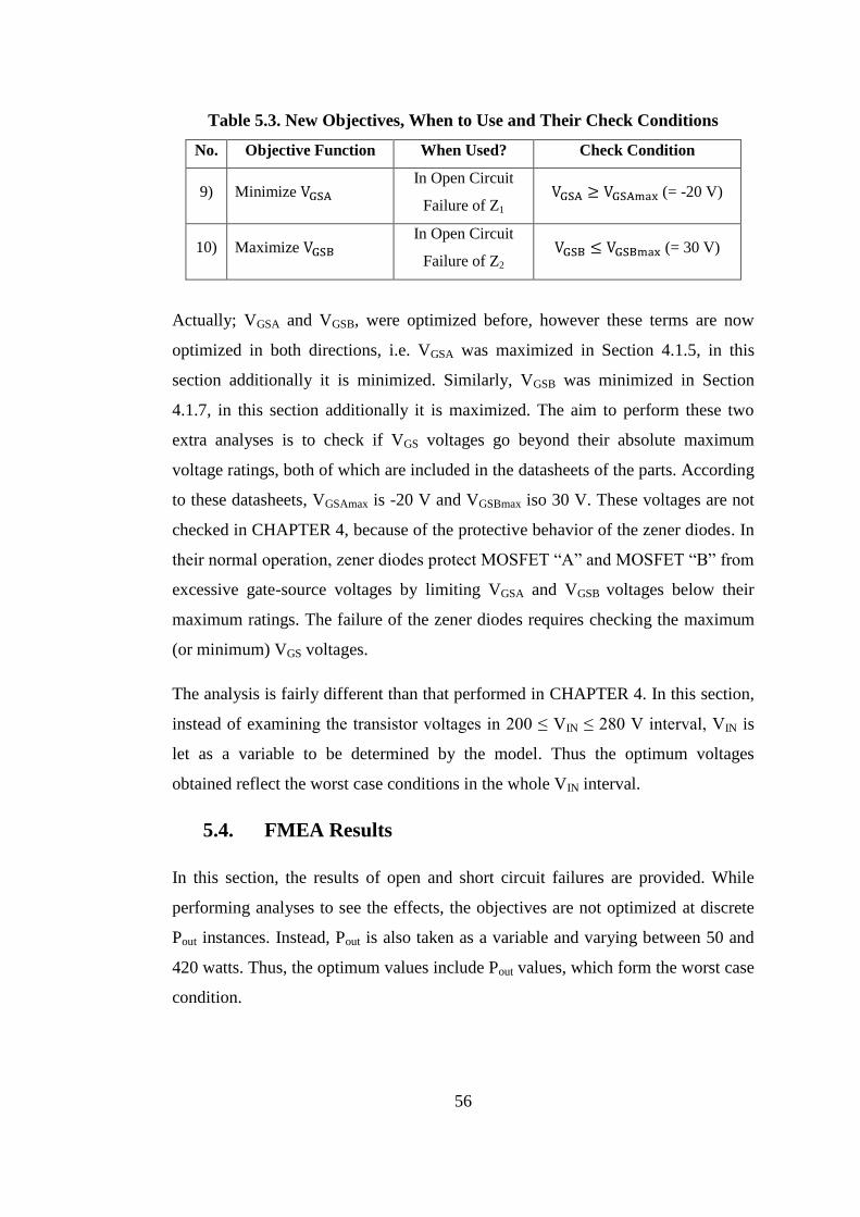
56
Table 5.3. New Objectives, When to Use and Their Check Conditions
No. Objective Function When Used? Check Condition
9) Minimize In Open Circuit
Failure of Z1 (= -20 V)
10) Maximize In Open Circuit
Failure of Z2 (= 30 V)
Actually; VGSA and VGSB, were optimized before, however these terms are now
optimized in both directions, i.e. VGSA was maximized in Section 4.1.5, in this
section additionally it is minimized. Similarly, VGSB was minimized in Section
4.1.7, in this section additionally it is maximized. The aim to perform these two
extra analyses is to check if VGS voltages go beyond their absolute maximum
voltage ratings, both of which are included in the datasheets of the parts. According
to these datasheets, VGSAmax is -20 V and VGSBmax iso 30 V. These voltages are not
checked in CHAPTER 4, because of the protective behavior of the zener diodes. In
their normal operation, zener diodes protect MOSFET “A” and MOSFET “B” from
excessive gate-source voltages by limiting VGSA and VGSB voltages below their
maximum ratings. The failure of the zener diodes requires checking the maximum
(or minimum) VGS voltages.
The analysis is fairly different than that performed in CHAPTER 4. In this section,
instead of examining the transistor voltages in 200 ≤ VIN ≤ 280 V interval, VIN is
let as a variable to be determined by the model. Thus the optimum voltages
obtained reflect the worst case conditions in the whole VIN interval.
5.4. FMEA Results
In this section, the results of open and short circuit failures are provided. While
performing analyses to see the effects, the objectives are not optimized at discrete
Pout instances. Instead, Pout is also taken as a variable and varying between 50 and
420 watts. Thus, the optimum values include Pout values, which form the worst case
condition.
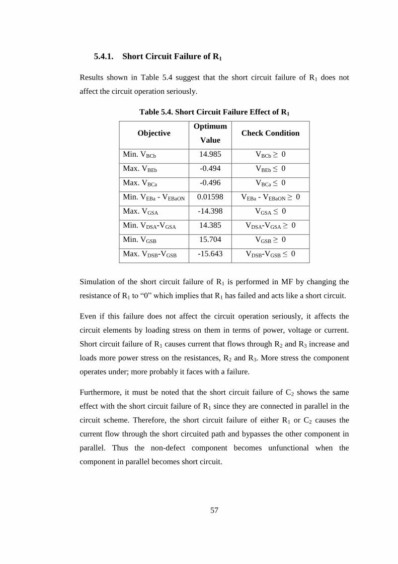
57
5.4.1. Short Circuit Failure of R1
Results shown in Table 5.4 suggest that the short circuit failure of R1 does not
affect the circuit operation seriously.
Table 5.4. Short Circuit Failure Effect of R1
Objective Optimum
Value Check Condition
Min. VBCb 14.985 VBCb ≥ 0
Max. VBEb -0.494 VBEb ≤ 0
Max. VBCa -0.496 VBCa ≤ 0
Min. VEBa - VEBaON 0.01598 VEBa - VEBaON ≥ 0
Max. VGSA -14.398 VGSA ≤ 0
Min. VDSA-VGSA 14.385 VDSA-VGSA ≥ 0
Min. VGSB 15.704 VGSB ≥ 0
Max. VDSB-VGSB -15.643 VDSB-VGSB ≤ 0
Simulation of the short circuit failure of R1 is performed in MF by changing the
resistance of R1 to “0” which implies that R1 has failed and acts like a short circuit.
Even if this failure does not affect the circuit operation seriously, it affects the
circuit elements by loading stress on them in terms of power, voltage or current.
Short circuit failure of R1 causes current that flows through R2 and R3 increase and
loads more power stress on the resistances, R2 and R3. More stress the component
operates under; more probably it faces with a failure.
Furthermore, it must be noted that the short circuit failure of C2 shows the same
effect with the short circuit failure of R1 since they are connected in parallel in the
circuit scheme. Therefore, the short circuit failure of either R1 or C2 causes the
current flow through the short circuited path and bypasses the other component in
parallel. Thus the non-defect component becomes unfunctional when the
component in parallel becomes short circuit.
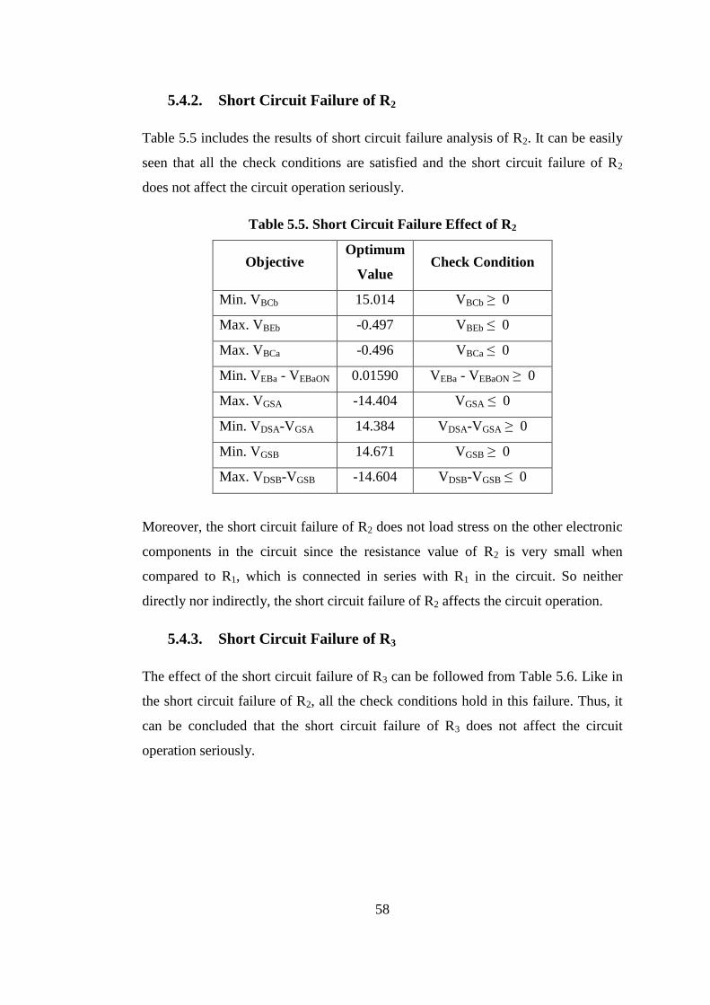
58
5.4.2. Short Circuit Failure of R2
Table 5.5 includes the results of short circuit failure analysis of R2. It can be easily
seen that all the check conditions are satisfied and the short circuit failure of R2
does not affect the circuit operation seriously.
Table 5.5. Short Circuit Failure Effect of R2
Objective Optimum
Value Check Condition
Min. VBCb 15.014 VBCb ≥ 0
Max. VBEb -0.497 VBEb ≤ 0
Max. VBCa -0.496 VBCa ≤ 0
Min. VEBa - VEBaON 0.01590 VEBa - VEBaON ≥ 0
Max. VGSA -14.404 VGSA ≤ 0
Min. VDSA-VGSA 14.384 VDSA-VGSA ≥ 0
Min. VGSB 14.671 VGSB ≥ 0
Max. VDSB-VGSB -14.604 VDSB-VGSB ≤ 0
Moreover, the short circuit failure of R2 does not load stress on the other electronic
components in the circuit since the resistance value of R2 is very small when
compared to R1, which is connected in series with R1 in the circuit. So neither
directly nor indirectly, the short circuit failure of R2 affects the circuit operation.
5.4.3. Short Circuit Failure of R3
The effect of the short circuit failure of R3 can be followed from Table 5.6. Like in
the short circuit failure of R2, all the check conditions hold in this failure. Thus, it
can be concluded that the short circuit failure of R3 does not affect the circuit
operation seriously.
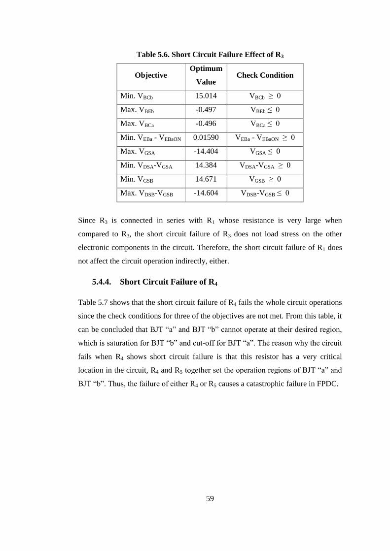
59
Table 5.6. Short Circuit Failure Effect of R3
Objective Optimum
Value Check Condition
Min. VBCb 15.014 VBCb ≥ 0
Max. VBEb -0.497 VBEb ≤ 0
Max. VBCa -0.496 VBCa ≤ 0
Min. VEBa - VEBaON 0.01590 VEBa - VEBaON ≥ 0
Max. VGSA -14.404 VGSA ≤ 0
Min. VDSA-VGSA 14.384 VDSA-VGSA ≥ 0
Min. VGSB 14.671 VGSB ≥ 0
Max. VDSB-VGSB -14.604 VDSB-VGSB ≤ 0
Since R3 is connected in series with R1 whose resistance is very large when
compared to R3, the short circuit failure of R3 does not load stress on the other
electronic components in the circuit. Therefore, the short circuit failure of R1 does
not affect the circuit operation indirectly, either.
5.4.4. Short Circuit Failure of R4
Table 5.7 shows that the short circuit failure of R4 fails the whole circuit operations
since the check conditions for three of the objectives are not met. From this table, it
can be concluded that BJT “a” and BJT “b” cannot operate at their desired region,
which is saturation for BJT “b” and cut-off for BJT “a”. The reason why the circuit
fails when R4 shows short circuit failure is that this resistor has a very critical
location in the circuit, R4 and R5 together set the operation regions of BJT “a” and
BJT “b”. Thus, the failure of either R4 or R5 causes a catastrophic failure in FPDC.
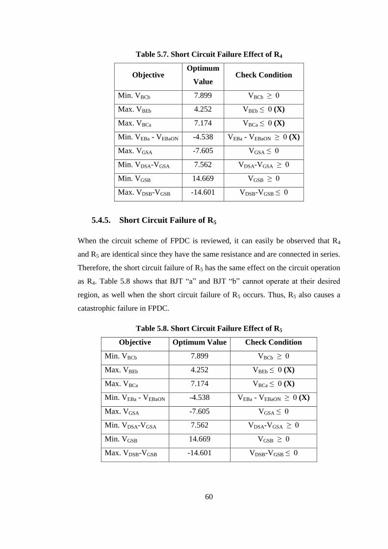
60
Table 5.7. Short Circuit Failure Effect of R4
Objective Optimum
Value Check Condition
Min. VBCb 7.899 VBCb ≥ 0
Max. VBEb 4.252 VBEb ≤ 0 (X)
Max. VBCa 7.174 VBCa ≤ 0 (X)
Min. VEBa - VEBaON -4.538 VEBa - VEBaON ≥ 0 (X)
Max. VGSA -7.605 VGSA ≤ 0
Min. VDSA-VGSA 7.562 VDSA-VGSA ≥ 0
Min. VGSB 14.669 VGSB ≥ 0
Max. VDSB-VGSB -14.601 VDSB-VGSB ≤ 0
5.4.5. Short Circuit Failure of R5
When the circuit scheme of FPDC is reviewed, it can easily be observed that R4
and R5 are identical since they have the same resistance and are connected in series.
Therefore, the short circuit failure of R5 has the same effect on the circuit operation
as R4. Table 5.8 shows that BJT “a” and BJT “b” cannot operate at their desired
region, as well when the short circuit failure of R5 occurs. Thus, R5 also causes a
catastrophic failure in FPDC.
Table 5.8. Short Circuit Failure Effect of R5
Objective Optimum Value Check Condition
Min. VBCb 7.899 VBCb ≥ 0
Max. VBEb 4.252 VBEb ≤ 0 (X)
Max. VBCa 7.174 VBCa ≤ 0 (X)
Min. VEBa - VEBaON -4.538 VEBa - VEBaON ≥ 0 (X)
Max. VGSA -7.605 VGSA ≤ 0
Min. VDSA-VGSA 7.562 VDSA-VGSA ≥ 0
Min. VGSB 14.669 VGSB ≥ 0
Max. VDSB-VGSB -14.601 VDSB-VGSB ≤ 0
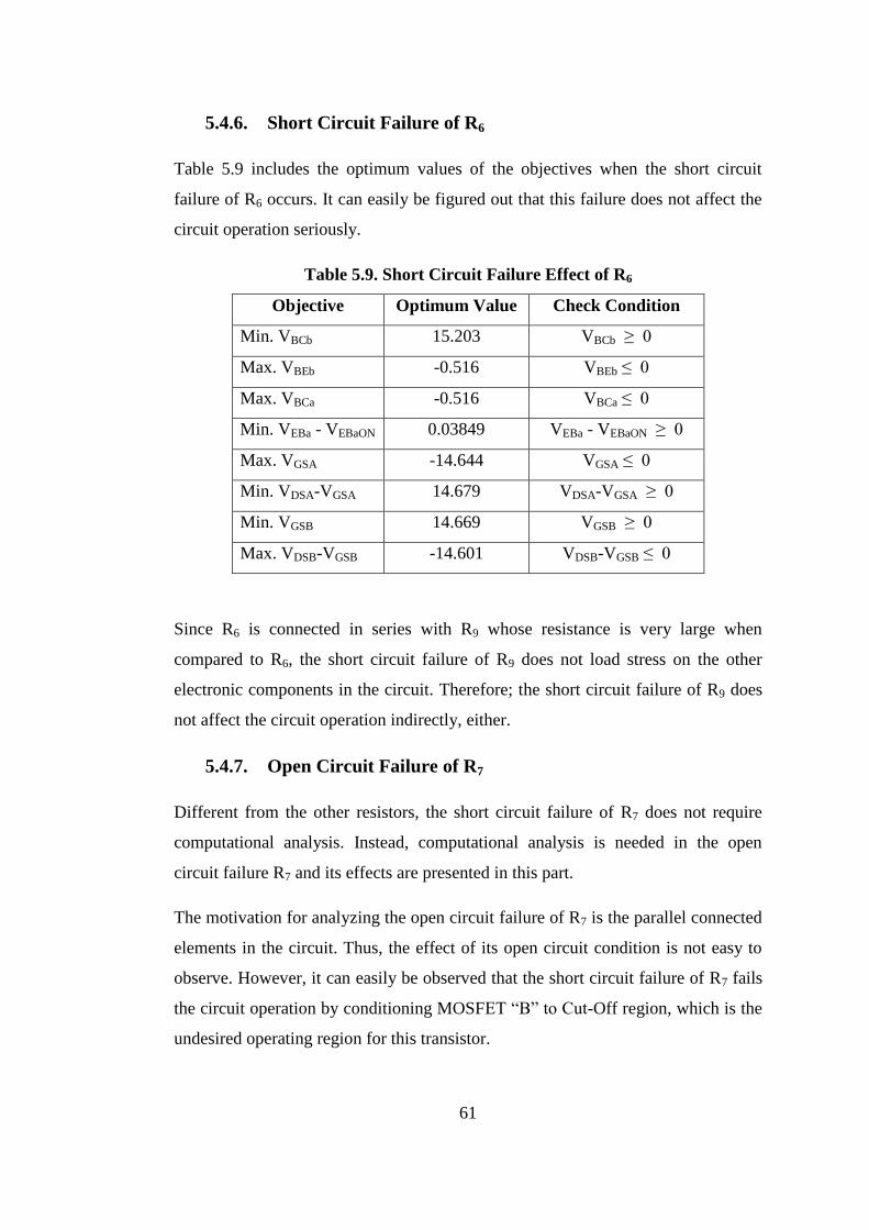
61
5.4.6. Short Circuit Failure of R6
Table 5.9 includes the optimum values of the objectives when the short circuit
failure of R6 occurs. It can easily be figured out that this failure does not affect the
circuit operation seriously.
Table 5.9. Short Circuit Failure Effect of R6
Objective Optimum Value Check Condition
Min. VBCb 15.203 VBCb ≥ 0
Max. VBEb -0.516 VBEb ≤ 0
Max. VBCa -0.516 VBCa ≤ 0
Min. VEBa - VEBaON 0.03849 VEBa - VEBaON ≥ 0
Max. VGSA -14.644 VGSA ≤ 0
Min. VDSA-VGSA 14.679 VDSA-VGSA ≥ 0
Min. VGSB 14.669 VGSB ≥ 0
Max. VDSB-VGSB -14.601 VDSB-VGSB ≤ 0
Since R6 is connected in series with R9 whose resistance is very large when
compared to R6, the short circuit failure of R9 does not load stress on the other
electronic components in the circuit. Therefore; the short circuit failure of R9 does
not affect the circuit operation indirectly, either.
5.4.7. Open Circuit Failure of R7
Different from the other resistors, the short circuit failure of R7 does not require
computational analysis. Instead, computational analysis is needed in the open
circuit failure R7 and its effects are presented in this part.
The motivation for analyzing the open circuit failure of R7 is the parallel connected
elements in the circuit. Thus, the effect of its open circuit condition is not easy to
observe. However, it can easily be observed that the short circuit failure of R7 fails
the circuit operation by conditioning MOSFET “B” to Cut-Off region, which is the
undesired operating region for this transistor.
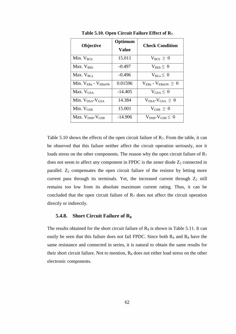
62
Table 5.10. Open Circuit Failure Effect of R7
Objective Optimum
Value Check Condition
Min. VBCb 15.011 VBCb ≥ 0
Max. VBEb -0.497 VBEb ≤ 0
Max. VBCa -0.496 VBCa ≤ 0
Min. VEBa - VEBaON 0.01596 VEBa - VEBaON ≥ 0
Max. VGSA -14.405 VGSA ≤ 0
Min. VDSA-VGSA 14.384 VDSA-VGSA ≥ 0
Min. VGSB 15.001 VGSB ≥ 0
Max. VDSB-VGSB -14.906 VDSB-VGSB ≤ 0
Table 5.10 shows the effects of the open circuit failure of R7. From the table, it can
be observed that this failure neither affect the circuit operation seriously, nor it
loads stress on the other components. The reason why the open circuit failure of R7
does not seem to affect any component in FPDC is the zener diode Z2 connected in
parallel. Z2 compensates the open circuit failure of the resistor by letting more
current pass through its terminals. Yet, the increased current through Z2 still
remains too low from its absolute maximum current rating. Thus, it can be
concluded that the open circuit failure of R7 does not affect the circuit operation
directly or indirectly.
5.4.8. Short Circuit Failure of R8
The results obtained for the short circuit failure of R8 is shown in Table 5.11. It can
easily be seen that this failure does not fail FPDC. Since both R6 and R8 have the
same resistance and connected in series, it is natural to obtain the same results for
their short circuit failure. Not to mention, R8 does not either load stress on the other
electronic components.
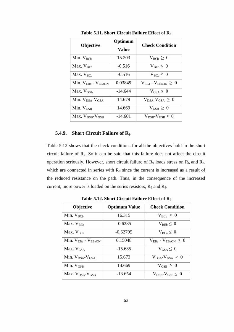
63
Table 5.11. Short Circuit Failure Effect of R8
Objective Optimum
Value Check Condition
Min. VBCb 15.203 VBCb ≥ 0
Max. VBEb -0.516 VBEb ≤ 0
Max. VBCa -0.516 VBCa ≤ 0
Min. VEBa - VEBaON 0.03849 VEBa - VEBaON ≥ 0
Max. VGSA -14.644 VGSA ≤ 0
Min. VDSA-VGSA 14.679 VDSA-VGSA ≥ 0
Min. VGSB 14.669 VGSB ≥ 0
Max. VDSB-VGSB -14.601 VDSB-VGSB ≤ 0
5.4.9. Short Circuit Failure of R9
Table 5.12 shows that the check conditions for all the objectives hold in the short
circuit failure of R9. So it can be said that this failure does not affect the circuit
operation seriously. However, short circuit failure of R9 loads stress on R6 and R8,
which are connected in series with R9 since the current is increased as a result of
the reduced resistance on the path. Thus, in the consequence of the increased
current, more power is loaded on the series resistors, R6 and R8.
Table 5.12. Short Circuit Failure Effect of R9
Objective Optimum Value Check Condition
Min. VBCb 16.315 VBCb ≥ 0
Max. VBEb -0.6285 VBEb ≤ 0
Max. VBCa -0.62795 VBCa ≤ 0
Min. VEBa - VEBaON 0.15048 VEBa - VEBaON ≥ 0
Max. VGSA -15.685 VGSA ≤ 0
Min. VDSA-VGSA 15.673 VDSA-VGSA ≥ 0
Min. VGSB 14.669 VGSB ≥ 0
Max. VDSB-VGSB -13.654 VDSB-VGSB ≤ 0
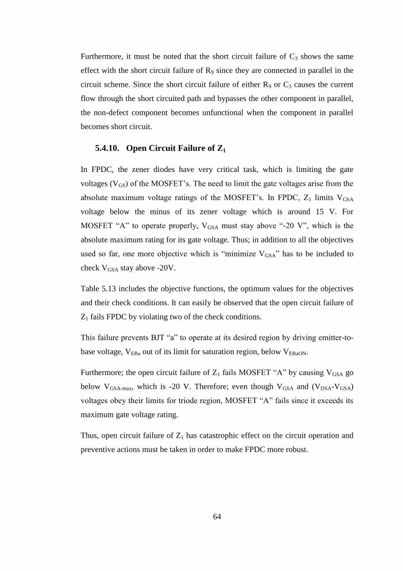
64
Furthermore, it must be noted that the short circuit failure of C3 shows the same
effect with the short circuit failure of R9 since they are connected in parallel in the
circuit scheme. Since the short circuit failure of either R9 or C3 causes the current
flow through the short circuited path and bypasses the other component in parallel,
the non-defect component becomes unfunctional when the component in parallel
becomes short circuit.
5.4.10. Open Circuit Failure of Z1
In FPDC, the zener diodes have very critical task, which is limiting the gate
voltages (VGS) of the MOSFET‟s. The need to limit the gate voltages arise from the
absolute maximum voltage ratings of the MOSFET‟s. In FPDC, Z1 limits VGSA
voltage below the minus of its zener voltage which is around 15 V. For
MOSFET “A” to operate properly, VGSA must stay above “-20 V”, which is the
absolute maximum rating for its gate voltage. Thus; in addition to all the objectives
used so far, one more objective which is “minimize VGSA” has to be included to
check VGSA stay above -20V.
Table 5.13 includes the objective functions, the optimum values for the objectives
and their check conditions. It can easily be observed that the open circuit failure of
Z1 fails FPDC by violating two of the check conditions.
This failure prevents BJT “a” to operate at its desired region by driving emitter-to-
base voltage, VEBa out of its limit for saturation region, below VEBaON.
Furthermore; the open circuit failure of Z1 fails MOSFET “A” by causing VGSA go
below VGSA-max, which is -20 V. Therefore; even though VGSA and (VDSA-VGSA)
voltages obey their limits for triode region, MOSFET “A” fails since it exceeds its
maximum gate voltage rating.
Thus, open circuit failure of Z1 has catastrophic effect on the circuit operation and
preventive actions must be taken in order to make FPDC more robust.
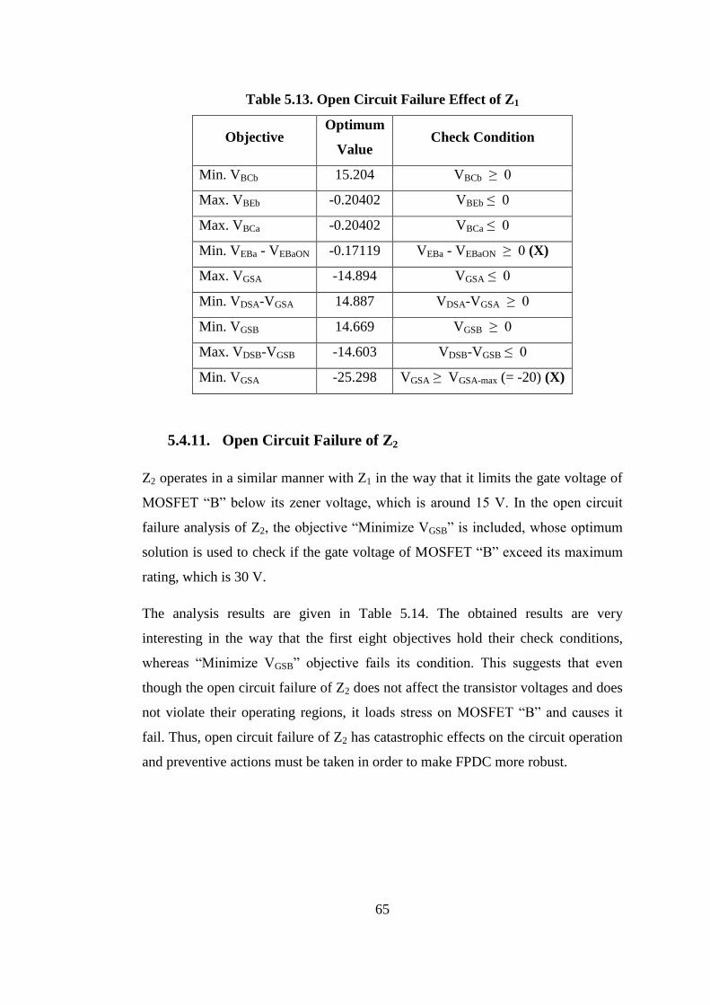
65
Table 5.13. Open Circuit Failure Effect of Z1
Objective Optimum
Value Check Condition
Min. VBCb 15.204 VBCb ≥ 0
Max. VBEb -0.20402 VBEb ≤ 0
Max. VBCa -0.20402 VBCa ≤ 0
Min. VEBa - VEBaON -0.17119 VEBa - VEBaON ≥ 0 (X)
Max. VGSA -14.894 VGSA ≤ 0
Min. VDSA-VGSA 14.887 VDSA-VGSA ≥ 0
Min. VGSB 14.669 VGSB ≥ 0
Max. VDSB-VGSB -14.603 VDSB-VGSB ≤ 0
Min. VGSA -25.298 VGSA ≥ VGSA-max (= -20) (X)
5.4.11. Open Circuit Failure of Z2
Z2 operates in a similar manner with Z1 in the way that it limits the gate voltage of
MOSFET “B” below its zener voltage, which is around 15 V. In the open circuit
failure analysis of Z2, the objective “Minimize VGSB” is included, whose optimum
solution is used to check if the gate voltage of MOSFET “B” exceed its maximum
rating, which is 30 V.
The analysis results are given in Table 5.14. The obtained results are very
interesting in the way that the first eight objectives hold their check conditions,
whereas “Minimize VGSB” objective fails its condition. This suggests that even
though the open circuit failure of Z2 does not affect the transistor voltages and does
not violate their operating regions, it loads stress on MOSFET “B” and causes it
fail. Thus, open circuit failure of Z2 has catastrophic effects on the circuit operation
and preventive actions must be taken in order to make FPDC more robust.
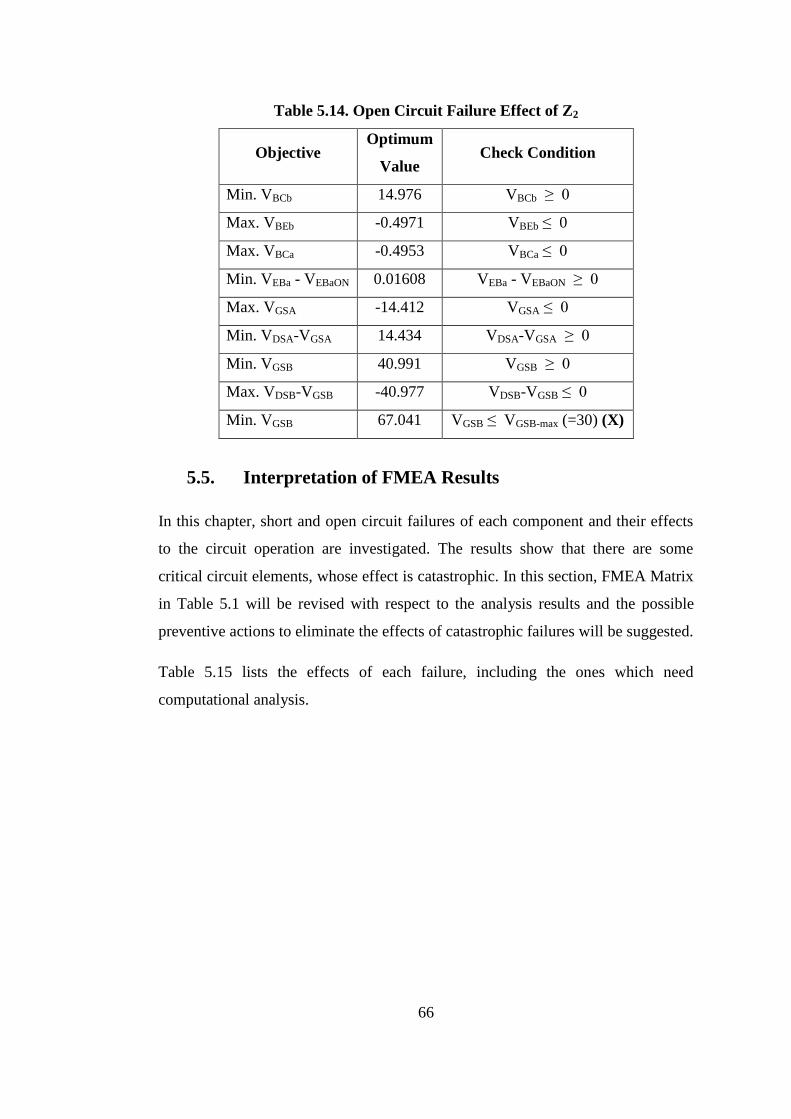
66
Table 5.14. Open Circuit Failure Effect of Z2
Objective Optimum
Value Check Condition
Min. VBCb 14.976 VBCb ≥ 0
Max. VBEb -0.4971 VBEb ≤ 0
Max. VBCa -0.4953 VBCa ≤ 0
Min. VEBa - VEBaON 0.01608 VEBa - VEBaON ≥ 0
Max. VGSA -14.412 VGSA ≤ 0
Min. VDSA-VGSA 14.434 VDSA-VGSA ≥ 0
Min. VGSB 40.991 VGSB ≥ 0
Max. VDSB-VGSB -40.977 VDSB-VGSB ≤ 0
Min. VGSB 67.041 VGSB ≤ VGSB-max (=30) (X)
5.5. Interpretation of FMEA Results
In this chapter, short and open circuit failures of each component and their effects
to the circuit operation are investigated. The results show that there are some
critical circuit elements, whose effect is catastrophic. In this section, FMEA Matrix
in Table 5.1 will be revised with respect to the analysis results and the possible
preventive actions to eliminate the effects of catastrophic failures will be suggested.
Table 5.15 lists the effects of each failure, including the ones which need
computational analysis.
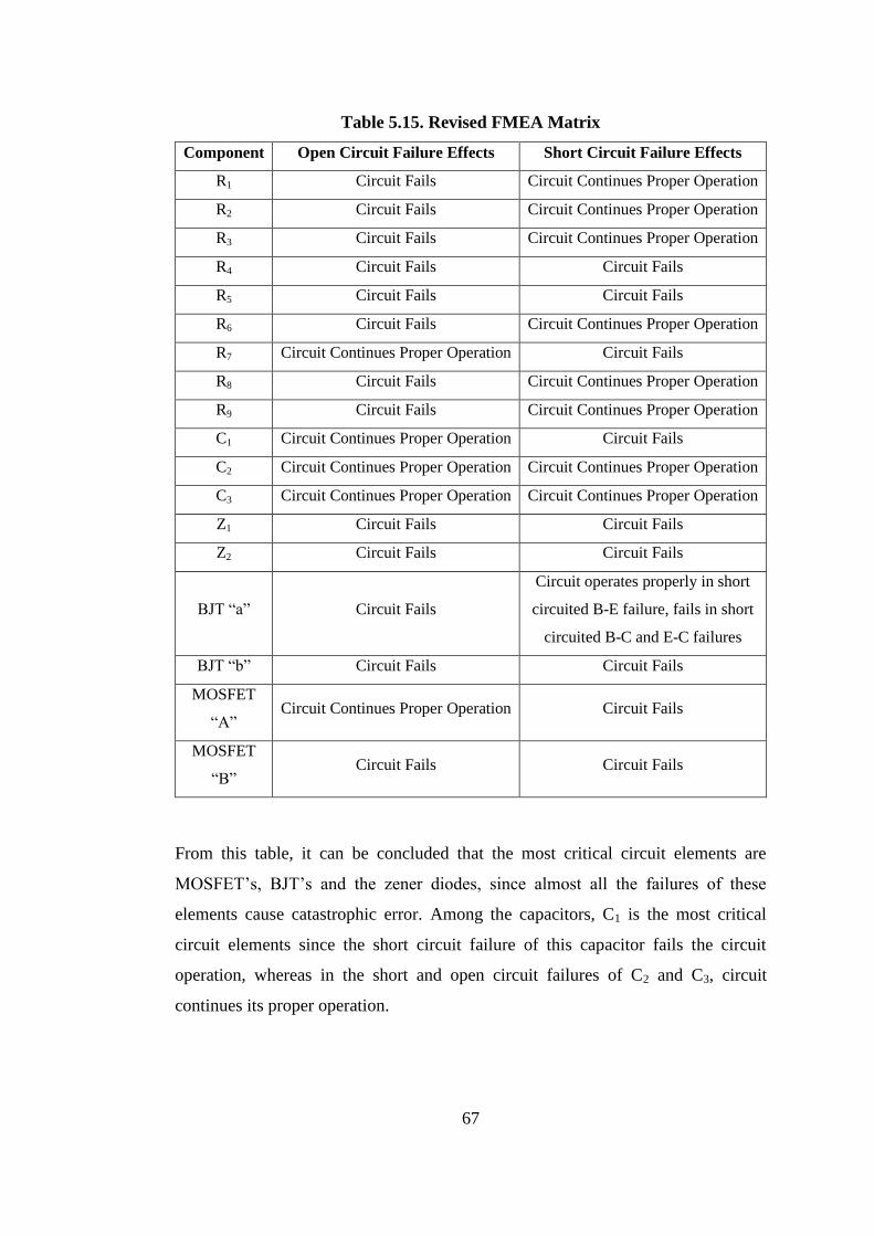
67
Table 5.15. Revised FMEA Matrix
Component Open Circuit Failure Effects Short Circuit Failure Effects
R1 Circuit Fails Circuit Continues Proper Operation
R2 Circuit Fails Circuit Continues Proper Operation
R3 Circuit Fails Circuit Continues Proper Operation
R4 Circuit Fails Circuit Fails
R5 Circuit Fails Circuit Fails
R6 Circuit Fails Circuit Continues Proper Operation
R7 Circuit Continues Proper Operation Circuit Fails
R8 Circuit Fails Circuit Continues Proper Operation
R9 Circuit Fails Circuit Continues Proper Operation
C1 Circuit Continues Proper Operation Circuit Fails
C2 Circuit Continues Proper Operation Circuit Continues Proper Operation
C3 Circuit Continues Proper Operation Circuit Continues Proper Operation
Z1 Circuit Fails Circuit Fails
Z2 Circuit Fails Circuit Fails
BJT “a” Circuit Fails
Circuit operates properly in short
circuited B-E failure, fails in short
circuited B-C and E-C failures
BJT “b” Circuit Fails Circuit Fails
MOSFET
“A” Circuit Continues Proper Operation Circuit Fails
MOSFET
“B” Circuit Fails Circuit Fails
From this table, it can be concluded that the most critical circuit elements are
MOSFET‟s, BJT‟s and the zener diodes, since almost all the failures of these
elements cause catastrophic error. Among the capacitors, C1 is the most critical
circuit elements since the short circuit failure of this capacitor fails the circuit
operation, whereas in the short and open circuit failures of C2 and C3, circuit
continues its proper operation.
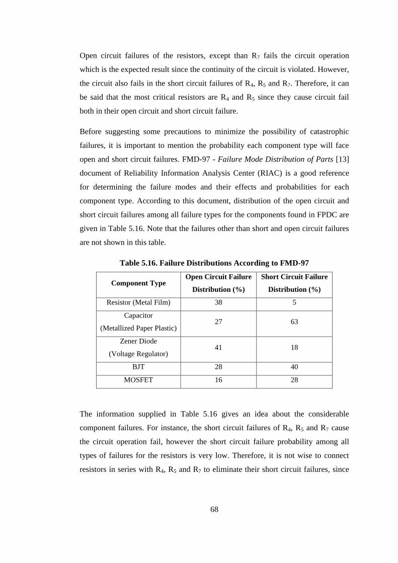
68
Open circuit failures of the resistors, except than R7 fails the circuit operation
which is the expected result since the continuity of the circuit is violated. However,
the circuit also fails in the short circuit failures of R4, R5 and R7. Therefore, it can
be said that the most critical resistors are R4 and R5 since they cause circuit fail
both in their open circuit and short circuit failure.
Before suggesting some precautions to minimize the possibility of catastrophic
failures, it is important to mention the probability each component type will face
open and short circuit failures. FMD-97 - Failure Mode Distribution of Parts [13]
document of Reliability Information Analysis Center (RIAC) is a good reference
for determining the failure modes and their effects and probabilities for each
component type. According to this document, distribution of the open circuit and
short circuit failures among all failure types for the components found in FPDC are
given in Table 5.16. Note that the failures other than short and open circuit failures
are not shown in this table.
Table 5.16. Failure Distributions According to FMD-97
Component Type Open Circuit Failure
Distribution (%)
Short Circuit Failure
Distribution (%)
Resistor (Metal Film) 38 5
Capacitor
(Metallized Paper Plastic) 27 63
Zener Diode
(Voltage Regulator) 41 18
BJT 28 40
MOSFET 16 28
The information supplied in Table 5.16 gives an idea about the considerable
component failures. For instance, the short circuit failures of R4, R5 and R7 cause
the circuit operation fail, however the short circuit failure probability among all
types of failures for the resistors is very low. Therefore, it is not wise to connect
resistors in series with R4, R5 and R7 to eliminate their short circuit failures, since
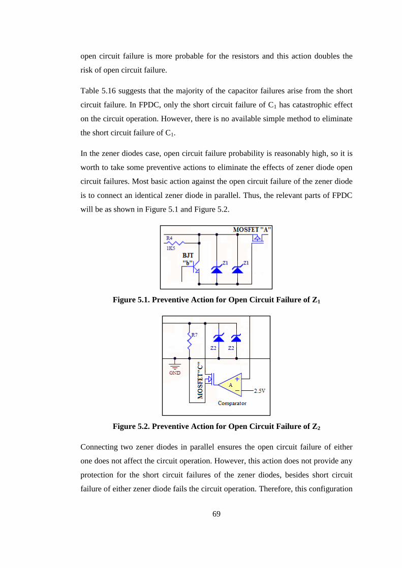
69
open circuit failure is more probable for the resistors and this action doubles the
risk of open circuit failure.
Table 5.16 suggests that the majority of the capacitor failures arise from the short
circuit failure. In FPDC, only the short circuit failure of C1 has catastrophic effect
on the circuit operation. However, there is no available simple method to eliminate
the short circuit failure of C1.
In the zener diodes case, open circuit failure probability is reasonably high, so it is
worth to take some preventive actions to eliminate the effects of zener diode open
circuit failures. Most basic action against the open circuit failure of the zener diode
is to connect an identical zener diode in parallel. Thus, the relevant parts of FPDC
will be as shown in Figure 5.1 and Figure 5.2.
Figure 5.1. Preventive Action for Open Circuit Failure of Z1
Figure 5.2. Preventive Action for Open Circuit Failure of Z2
Connecting two zener diodes in parallel ensures the open circuit failure of either
one does not affect the circuit operation. However, this action does not provide any
protection for the short circuit failures of the zener diodes, besides short circuit
failure of either zener diode fails the circuit operation. Therefore, this configuration
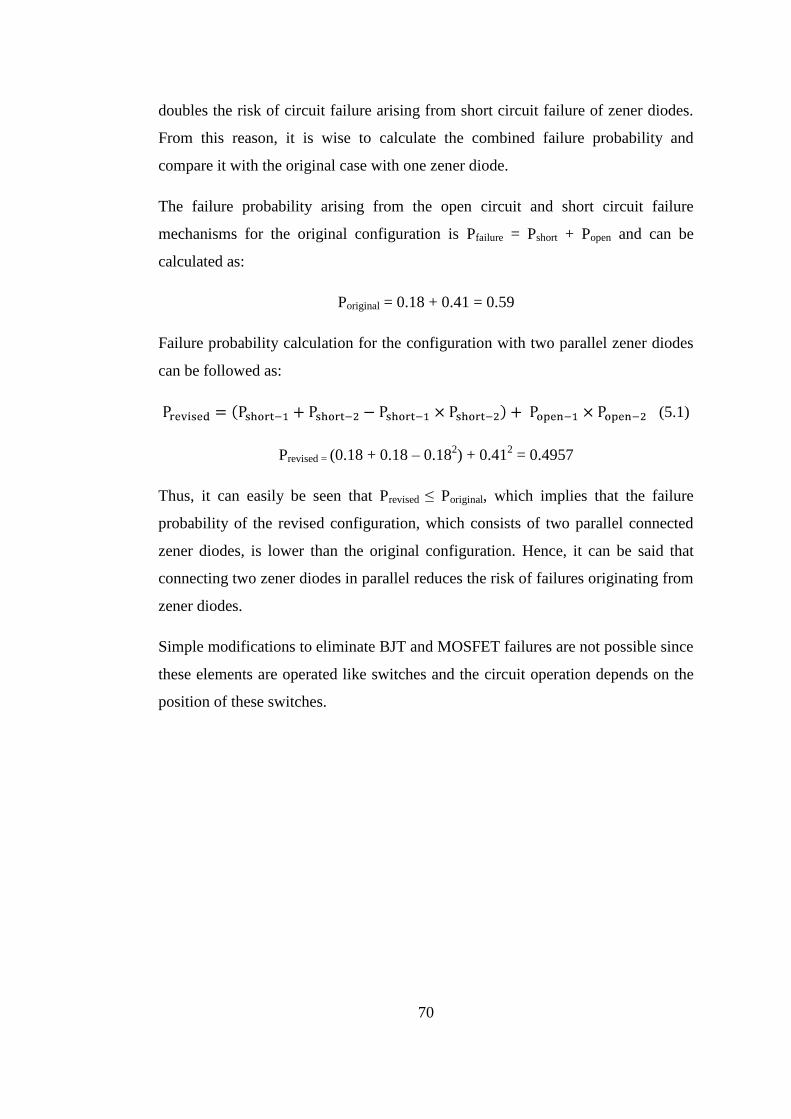
70
doubles the risk of circuit failure arising from short circuit failure of zener diodes.
From this reason, it is wise to calculate the combined failure probability and
compare it with the original case with one zener diode.
The failure probability arising from the open circuit and short circuit failure
mechanisms for the original configuration is Pfailure = Pshort + Popen and can be
calculated as:
Poriginal = 0.18 + 0.41 = 0.59
Failure probability calculation for the configuration with two parallel zener diodes
can be followed as:
(5.1)
Prevised = (0.18 + 0.18 – 0.182) + 0.41
2 = 0.4957
Thus, it can easily be seen that Prevised ≤ Poriginal, which implies that the failure
probability of the revised configuration, which consists of two parallel connected
zener diodes, is lower than the original configuration. Hence, it can be said that
connecting two zener diodes in parallel reduces the risk of failures originating from
zener diodes.
Simple modifications to eliminate BJT and MOSFET failures are not possible since
these elements are operated like switches and the circuit operation depends on the
position of these switches.
71
CHAPTER 6
CONCLUSION
Circuit reliability analysis is a critical application that is performed frequently
especially in analog circuit design phase. This analysis becomes more of an issue in
the circuits which have critical tasks. In this thesis, the reliability analysis of the
Fuel Pump Driver Circuit (FPDC) is examined. This circuit is responsible from
supplying the power that the fuel pump requires in order to pump the required
amount of fuel to the turbojet engine. FPDC has a very critical mission in such a
way that if this circuit fails, the turbojet engine rotation will slow down and the air
vehicle will face the risk of falling. Therefore, it is desirable to confirm that the
circuit operates properly in the worst case conditions, or even at the failure of some
components in the circuit.
The primary tools for circuit reliability can be counted as reliability allocation and
prediction, worst case circuit tolerance analysis, failure modes and effects analysis
and fault-tree analysis. The applicable reliability analyses for FPDC are the worst
case circuit tolerance analysis and the failure modes and effects analysis. During
the reliability analysis of FPDC, these two analyses are performed to observe the
effects and conditions are checked if the circuit operates correctly.
Firstly, the worst case circuit tolerance analysis of FPDC has been performed. This
analysis investigates the effects of the tolerant resistances, different temperature
and input voltage values on the circuit operation.
72
In the worst case analysis of FPDC, the effort is to find the input voltage,
temperature and resistance values that constitute the worst case condition for the
defined objective function. Once the optimum value for the objective function is
reached, we check if it remains in the feasible interval. This analysis is repeated for
eight objectives, each of which sets a check condition for the operating region of a
transistor. These analyses are run utilizing two software programs: MATLAB and
ModeFRONTIER. Parameter values are generated in ModeFRONTIER and these
values are sent to MATLAB to solve the equations defined in it.
The worst case circuit analysis results show that FPDC operates with no problem in
the whole band of resistance tolerances, temperature and input voltage interval.
Therefore, we can conclude that FPDC withstands all variations in the circuit.
Optimum objective values are drawn in power output band and the most critical
power requirement condition has been determined to be 50 W, which is the lower
bound for the power output. Similarly, the most critical temperature seems to be -
30 °C since it is the binding constraint for four of the objectives.
After completing the worst case analysis, the failure modes and effects analysis is
performed. This analysis is fulfilled by examining the short circuit and open circuit
failures of all the components used in the circuit. However, computational analysis
is performed only for the failures, whose effect is not obvious and cannot be
observed by inspection. The computational analyses are also performed in
MATLAB and ModeFRONTIER programs. The components whose failure cause
catastrophic circuit failure have been determined according to the FMEA results.
The failure distributions of each component type per FMD-97 document have been
introduced and some preventive actions are suggested to minimize the number of
catastrophic failures taking into consideration the failure distributions.
In real world applications, Monte Carlo analysis is used frequently to perform
circuit worst case analysis and failure modes and effects analysis. Besides, basic
circuit simulation tools (more generally SPICE tools) depend on Monte Carlo
analysis while carrying out worst case circuit tolerance analysis. Nevertheless,
Monte Carlo analysis is a probabilistic method and does not guarantee to reach the
73
worst case conditions. In this study, by moving the circuit analysis to a
deterministic model and presenting an alternative method for circuit reliability
analysis, the real worst case conditions have been reached. Therefore, it can be said
that it is ensured that FPDC operates properly in the desired region in any condition
with certainty depending on the results obtained with this method.
An initial effort has been made to reflect the equations that govern the circuit
operation; this is the most time consuming part of this study. However, once the
circuit equalities are introduced to MATLAB and ModeFRONTIER, this method
provides great flexibility and enables the user to reach the worst case results in a
meaningful time.
Furthermore, transistors are also included in the tolerance analysis in this study. As
far as we know, no other study considered the operating regions of the transistors in
the reliability analysis applications. In this thesis, the reliability analysis is
performed on the basis of the operating regions of the transistors. The impression
about the correct operation of the circuit is obtained from the operating regions of
the transistors.
The method used in this study can be applied to other circuits, which do not include
complex components like integrated circuits and operate in the steady state
conditions. In the case of larger electronic circuits, this method can be applied with
no problem by decomposing the circuit into smaller fragments so that the solution
times do not increase seriously and complete reliability analysis of the circuit can
be performed by composing the results obtained from each fragment.
To apply the method presented in this study, the steady state conditions are
necessary, since timing is not considered in the calculations and it is assumed that
no transitions occur in the circuit. However, the circuits which are used for
switching application usually have two states: ON and OFF condition. In FPDC
case, there are two states, as well. The investigated state in this study is the default
ON state, which includes the normal operating conditions. Unless the input voltage
VIN exceeds 280 V, this state is preserved and the steady state conditions are
reached if VIN does not vary in time. In this thesis, the analyses are performed
74
assuming that VIN does not vary in time and remains below 280 V. The OFF state,
which includes the operation where VIN is larger than 280 V, is aimed to be
analyzed as well. But because of the lack of steady state conditions in that state, the
analyses with the methods used in ON state got difficult to use and the analyses for
the OFF state is excluded from the content of this study. However as a future study,
it may be aimed to analyze OFF state of FPDC presenting new methods and
complete reliability analysis of this circuit.
75
REFERENCES
[1] Dreyer, A., Interval Analysis of Linear Analog Circuits, 12th GAMM -
IMACS International Symposium on Scientific Computing, Computer Arithmetic
and Validated Numerics (2006), 14-22.
[2] Femia, N. and Spagnuolo, G., True Worst-Case Circuit Tolerance Analysis
Using Genetic Algorithms and Affine Arithmetic, IEEE Transactions on Circuits
and Systems I: Fundamental Theory and Applications, 47-9 (2000), 1285-1296.
[3] Gummel, H.K. and Poon, H.C., An Integral Charge Control Model of
Bipolar Transistors, Bell Systems Technical Journal, 49 (1970), 827-852.
[4] Kolev, L., Worst-Case Tolerance Analysis of Linear DC and AC Electric
Circuits, IEEE Transactions on Circuits and Systems I: Fundamental Theory and
Applications, 49-12 (2002), 1693-1701.
[5] Liu, F. and Ozev, S., Statistical Test Development for Analog Circuits
Under High Process Variations, IEEE Transactions On Computer-Aided Design of
Integrated Circuits and Systems, 26-8 (2007), 1465-1477.
[6] Nelder, J.A. and Mead, R.A., Simplex for Function Minimization, The
Computer Journal, 7 (1965), 308–313.
[7] Spence, R. and Soin R., Tolerance Design of Electronic Circuits, Addison-
Wesley (1988),
[8] Tian, M.W. and Shi, R.C.-J., Worst Case Tolerance Analysis of Linear
Analog Circuits Using Sensitivity Bands, IEEE Transactions on Circuits and
Systems I: Fundamental Theory and Applications, 47-8 (2000), 1138-1145.
[9] Tian, M.W., Ling, X.-T. and Liu, R.-W., Novel Methods for Circuit Worst-
Case Tolerance Analysis, IEEE Transactions on Circuits and Systems I:
Fundamental Theory and Applications, 43-4 (1996), 272-278.
76
[10] Wang, P. and Yang, S., A New Diagnosis Approach for Handling Tolerance
in Analog and Mixed-Signal Circuits by Using Fuzzy Math, IEEE Transactions on
Circuits and Systems – I, 52-10 (2005), 2118-2127.
[11] White, R. V., An Introduction to Six Sigma With a Design Example, IEEE
Applied Power Electronics Conference and Exposition, (1992), 28-35.
[12] White, R. V., Component Tolerance And Circuit Performance: A Case
Study, IEEE Applied Power Electronics Conference and Exposition, (1993), 922-
927.
[13] Reliability Prediction of Electronic Equipment, MIL-HDBK-217F, U.S.
Department of Defense (1991).
[14] Electronic Reliability Design Handbook, MIL-HDBK-338B, U.S.
Department of Defense (1998).
[15] Failure Mode/Mechanism Distributions, FMD-97, Reliability Information
Analysis Center (RIAC), Rome (NY, USA) (1998), sample version available online at
http://src.alionscience.com/pdf/RAC-1ST/FMD97_1ST.pdf (last accessed 23rd
January 2011).
[16] Worst Case Circuit Analysis Application Guidelines, Reliability
Information Analysis Center (RIAC), Rome (NY, USA) (1993)
[17] ZXTC2063E6, Complementary Medium Power Transistors Datasheet
(2007), available at http://www.diodes.com/datasheets/ZXTC2063E6.pdf (last
accessed 25th January 2011).
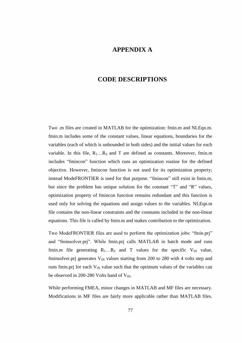
77
APPENDIX A
CODE DESCRIPTIONS
Two .m files are created in MATLAB for the optimization: fmin.m and NLEqn.m.
fmin.m includes some of the constant values, linear equations, boundaries for the
variables (each of which is unbounded in both sides) and the initial values for each
variable. In this file, R1…R9 and T are defined as constants. Moreover, fmin.m
includes “fmincon” function which runs an optimization routine for the defined
objective. However, fmincon function is not used for its optimization property;
instead ModeFRONTIER is used for that purpose. “fmincon” still exist in fmin.m,
but since the problem has unique solution for the constant “T” and “R” values,
optimization property of fmincon function remains redundant and this function is
used only for solving the equations and assign values to the variables. NLEqn.m
file contains the non-linear constraints and the constants included in the non-linear
equations. This file is called by fmin.m and makes contribution to the optimization.
Two ModeFRONTIER files are used to perform the optimization jobs: “fmin.prj”
and “fminsolver.prj”. While fmin.prj calls MATLAB in batch mode and runs
fmin.m file generating R1…R9 and T values for the specific VIN value,
fminsolver.prj generates VIN values starting from 200 to 280 with 4 volts step and
runs fmin.prj for each VIN value such that the optimum values of the variables can
be observed in 200-280 Volts band of VIN.
While performing FMEA, minor changes in MATLAB and MF files are necessary.
Modifications in MF files are fairly more applicable rather than MATLAB files.
78
This is because MF has good interface and the modifications can be done easily
and quickly. Not modifying the MATLAB codes is highly desirable; however it is
not possible for the open circuit failures of the zener diodes, Z1 and Z2. Fortunately,
failures of the resistors can be simulated only by modifying the MF file, fmin.prj. It
is simply applied by changing the resistance value of short circuited resistor to zero
and open circuited resistor to infinity instead of defining it in an interval, like what
is done in tolerance analysis case.
Also in FMEA, VIN is let as a variable to be determined by the model. This
modification is also introduced in fmin.prj defining VIN as a variable, varying in
200-280V interval.
The content of fmin.m and NLEqn.m is provided in the following pages. Note that
the scripts after “%” sign stand for the comments
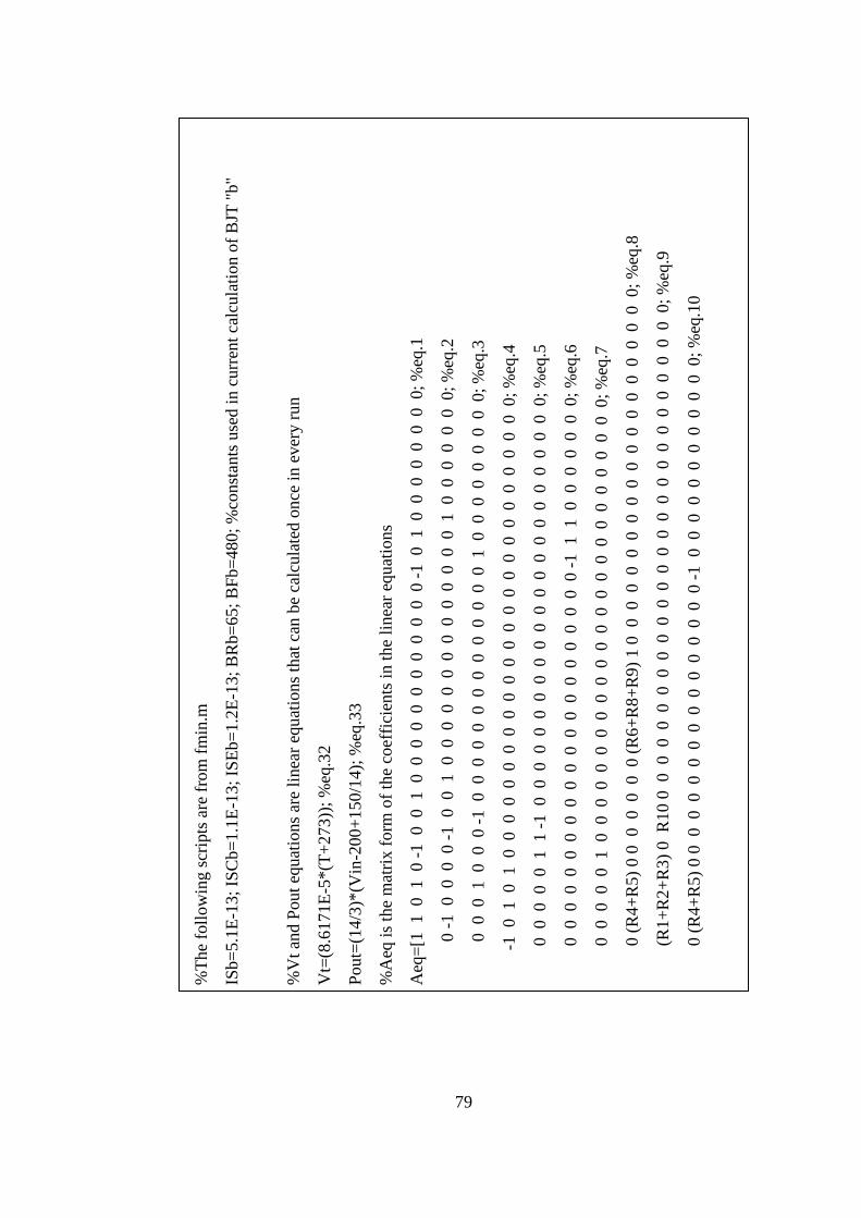
79
%T
he
foll
ow
ing s
crip
ts a
re f
rom
fm
in.m
ISb=
5.1
E-1
3;
ISC
b=
1.1
E-1
3;
ISE
b=
1.2
E-1
3;
BR
b=
65;
BF
b=
480;
%co
nst
ants
use
d i
n c
urr
ent
calc
ula
tion o
f B
JT "
b"
%V
t an
d P
out
equat
ions
are
linea
r eq
uat
ions
that
can
be
calc
ula
ted o
nce
in
ever
y r
un
Vt=
(8.6
171E
-5*(T
+273))
; %
eq.3
2
Pout=
(14/3
)*(V
in-2
00+
150/1
4);
%eq
.33
%A
eq i
s th
e m
atri
x f
orm
of
the
coef
fici
ents
in t
he
linea
r eq
uat
ions
Aeq
=[1
1 0 1 0 -
1 0 0
1 0 0 0 0 0 0
0 0 0 0 0 0 -
1 0 1 0 0 0 0 0 0 0 0;
%eq
.1
0 -
1 0 0 0 0 -
1 0
0 1 0 0 0 0 0 0 0 0 0 0 0 0 0 0 1 0 0 0 0 0 0 0;
%eq
.2
0 0 0 1 0 0 0 -
1 0 0 0 0 0 0 0 0 0 0 0 0 0 0 1 0 0
0 0 0 0 0 0 0;
%eq
.3
-1
0 1 0 1 0 0 0 0 0 0 0 0 0 0 0 0 0 0 0 0 0 0 0 0 0 0
0 0 0 0 0;
%eq
.4
0
0 0 0 0 1 1 -
1 0 0 0 0 0 0 0 0 0 0 0 0 0 0 0 0 0 0 0 0 0 0 0 0;
%eq
.5
0
0 0 0 0 0 0 0 0 0 0 0 0 0 0 0 0 0 0 0 0 0 -
1 1 1 0 0 0 0 0 0 0;
%eq
.6
0
0 0 0 0 1 0 0 0 0 0 0 0 0 0 0 0 0 0 0 0 0 0 0 0 0 0 0 0 0 0 0;
%eq
.7
0
(R
4+
R5)
0 0
0 0 0 0 0 (
R6
+R
8+
R9)
1 0
0 0 0 0 0 0 0 0 0 0 0 0 0 0 0 0 0 0 0 0;
%eq
.8
(
R1+
R2+
R3)
0 R
10 0
0 0 0 0 0 0 0 0 0 0 0 0 0 0 0 0 0 0 0 0 0 0 0 0 0 0 0 0;
%eq
.9
0
(R
4+
R5)
0 0
0 0 0 0 0 0 0 0 0 0 0
0 0 0 0 -
1 0 0 0 0 0 0 0 0 0 0 0 0;
%eq
.10
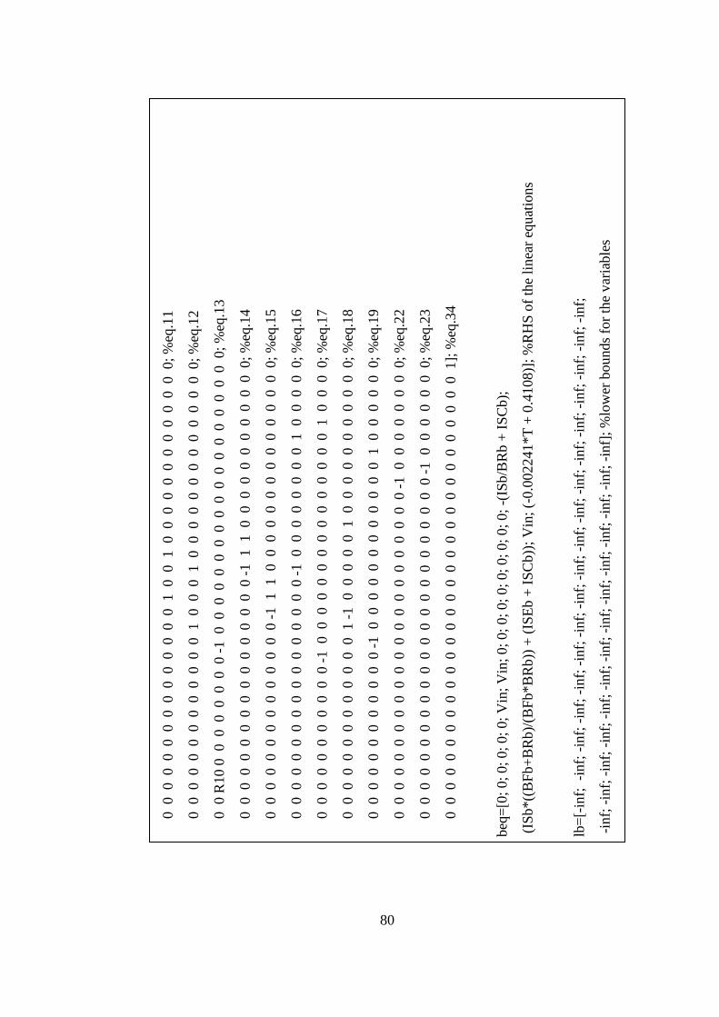
80
0
0 0 0 0 0 0 0 0 0 0 0 0 0 0 1 0 0 1 0 0 0 0 0 0 0 0 0 0 0 0 0;
%eq
.11
0
0 0 0 0 0 0 0 0 0 0 0 0 1 0 0 0 1 0 0 0 0 0 0 0 0 0 0 0 0 0 0;
%eq
.12
0
0 R
10 0
0 0 0 0
0 0 0 -
1 0 0 0 0 0 0 0 0 0 0 0 0 0 0 0 0 0 0 0 0;
%eq
.13
0
0 0 0 0 0 0 0 0 0 0 0
0 0 0 0 0 -
1 1 1 0 0 0 0 0 0 0 0 0 0 0 0;
%eq
.14
0
0 0 0 0 0 0 0 0 0 0 0 0 0 -
1 1 1 0 0 0 0 0 0 0 0 0 0 0 0 0 0 0;
%eq
.15
0
0 0 0 0 0 0 0 0 0 0 0 0 0 0 0 0 -
1 0 0 0 0 0 0 0 0 1 0 0 0 0 0;
%eq
.16
0
0 0 0 0 0 0 0 0 0 0 -
1 0 0 0 0 0 0 0 0 0 0 0 0 0 0 0 1 0 0 0 0;
%eq
.17
0
0 0 0 0 0 0 0 0 0 0 0
0 1 -
1 0 0 0 0 0 1 0 0 0 0 0 0 0 0 0 0 0;
%eq
.18
0
0 0 0 0 0 0 0 0 0 0 0 -
1 0 0 0 0 0 0 0 0 0 0 0 0 1 0 0 0 0 0 0;
%eq
.19
0
0 0 0 0 0 0 0 0 0 0 0 0 0 0 0 0 0 0 0 0 0 0 -
1 0 0 0 0 0 0 0 0;
%eq
.22
0
0 0 0 0 0 0 0 0 0 0 0 0 0 0 0 0 0 0 0 0 0 0 0 -
1 0 0 0 0 0 0 0;
%eq
.23
0
0 0 0 0 0 0 0 0 0 0 0 0 0 0 0 0 0 0 0 0 0 0 0 0 0 0 0 0 0 0 1];
%eq
.34
beq
=[0
; 0;
0;
0;
0;
0;
Vin
; V
in;
0;
0;
0;
0;
0;
0;
0;
0;
0;
0;
-(IS
b/B
Rb +
IS
Cb);
(IS
b*((
BF
b+
BR
b)/
(BF
b*B
Rb))
+ (
ISE
b +
IS
Cb))
; V
in;
(-0.0
02241*T
+ 0
.4108)]
; %
RH
S o
f th
e li
nea
r eq
uat
ions
lb=
[-in
f;
-inf;
-in
f; -
inf;
-in
f; -
inf;
-in
f; -
inf;
-in
f; -
inf;
-in
f; -
inf;
-in
f; -
inf;
-in
f; -
inf;
-in
f; -
inf;
-in
f; -
inf;
-in
f; -
inf;
-in
f; -
inf;
-in
f; -
inf;
-in
f; -
inf;
-in
f; -
inf;
-in
f; -
inf]
; %
low
er b
ounds
for
the
var
iable
s
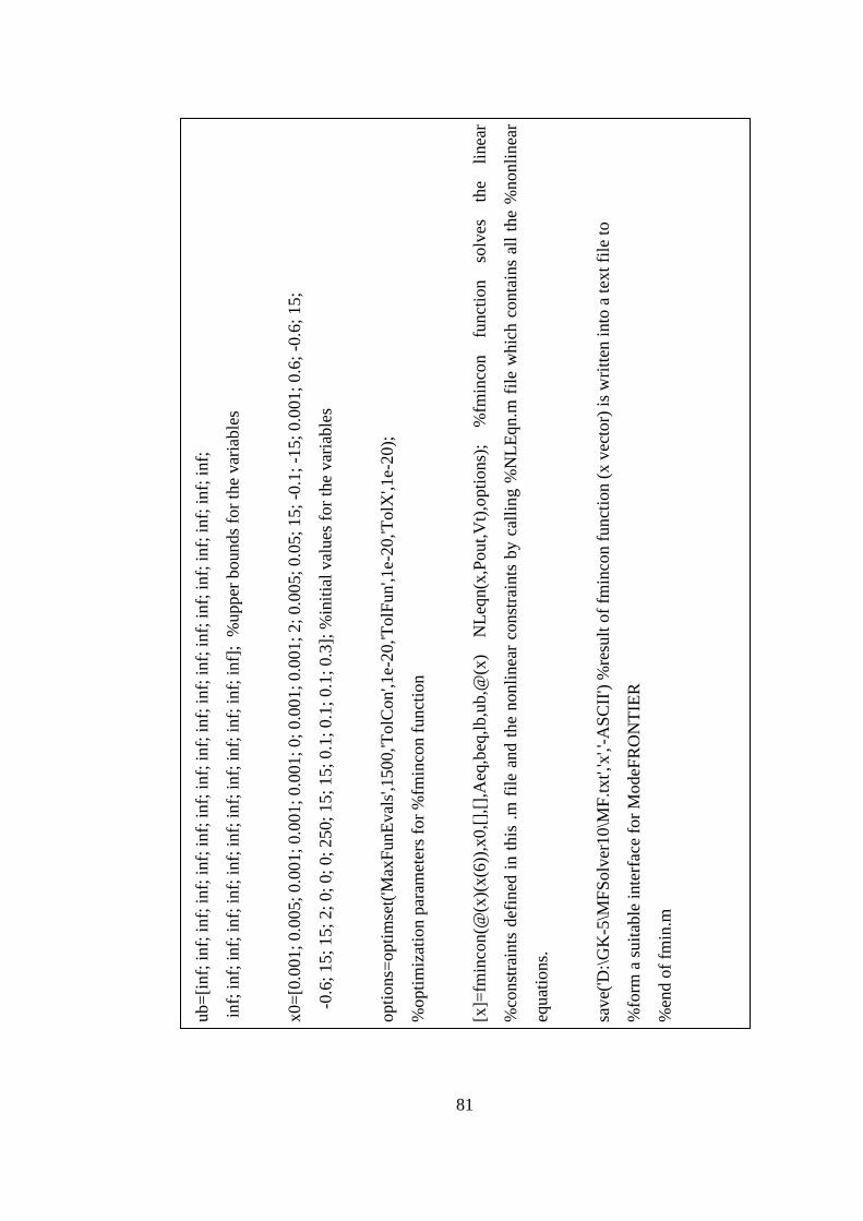
81
ub=
[inf;
inf;
inf;
inf;
inf;
inf;
inf;
inf;
inf;
inf;
inf;
inf;
inf;
inf;
inf;
inf;
inf;
inf;
inf;
inf;
in
f; i
nf;
inf;
inf;
inf;
inf;
in
f; i
nf;
inf;
inf;
inf;
inf]
; %
upper
bounds
for
the
var
iable
s
x0=
[0.0
01;
0.0
05;
0.0
01;
0.0
01;
0.0
01;
0;
0.0
01;
0.0
01
; 2;
0.0
05;
0.0
5;
15;
-0.1
; -1
5;
0.0
01;
0.6
; -0
.6;
15;
-
0.6
; 15;
15;
2;
0;
0;
0;
250;
15;
15;
0.1
; 0.1
; 0.1
; 0.3
]; %
init
ial
val
ues
for
the
var
iable
s
opti
ons=
opti
mse
t('M
axF
unE
val
s',1
500,'T
olC
on',1
e-20,'T
olF
un',1
e-20,'T
olX
',1e-
20);
%opti
miz
atio
n p
aram
eter
s fo
r %
fmin
con f
un
ctio
n
[x]=
fmin
con
(@(x
)(x(6
)),x
0,[
],[]
,Aeq
,beq
,lb,u
b,@
(x)
NL
eqn(x
,Pout,
Vt)
,opti
ons)
; %
fmin
con
funct
ion
solv
es
the
linea
r
%co
nst
rain
ts d
efin
ed i
n t
his
.m
fil
e an
d t
he
nonli
nea
r co
nst
rain
ts b
y c
alli
ng %
NL
Eqn.m
fil
e w
hic
h c
onta
ins
all
the
%nonli
nea
r
equat
ions.
save(
'D:\
GK
-5\M
FS
olv
er10
\MF
.txt','x
','-A
SC
II')
%re
sult
of
fmin
con f
un
ctio
n (
x v
ecto
r) i
s w
ritt
en i
nto
a t
ext
file
to
%fo
rm a
suit
able
inte
rfac
e fo
r M
odeF
RO
NT
IER
%en
d o
f fm
in.m
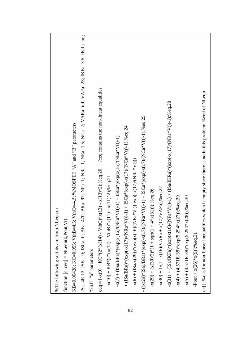
82
%T
he
foll
ow
ing s
crip
ts a
re f
rom
NL
eqn.m
funct
ion [
c, c
eq]
= N
Leq
n(x
,Pout,
Vt)
KB
=0.0
0428;
KC
=0.9
55;
Vth
B=
4.5
; V
thC
=-4
.5;
%M
OS
FE
T “
A”
and “
B”
par
amet
ers
ISa=
4E
-13;
ISE
a=0;
ISC
a=0;
BF
a=470;
BR
a=97;
NF
a=1;
NR
a=1,
NE
a=1.5
; N
Ca=
2;
VA
Ra=
inf;
VA
Fa=
23;
IKF
a=3.5
; IK
Ra=
inf;
%B
JT “
a” p
aram
eter
s
ceq =
[-x
(9)
+ K
C*(2
*(x
(14)
- V
thC
)*x(1
3)
- x(1
3)^
2);
%eq
.20
/ceq
conta
ins
the
non
-lin
ear
equ
alit
ies
-x
(10)
+ K
B*(2
*(x
(12
) -
Vth
B)*
x(1
1)
- x(1
1)^
2);
%eq
.21
-x
(7)
+ (
ISa/
BF
a)*(e
xp(x
(16)/
(NF
a*V
t))-
1)
+ I
SE
a*(e
xp(x
(16
)/(N
Ea*
Vt)
)-1)
+
(IS
a/B
Ra)
*(e
xp(-
x(1
7)/
(NR
a*V
t))-
1)
+ I
SC
a*(e
xp(-
x(1
7)/
(NC
a*V
t))-
1);
%eq
.24
-x
(6)
+ (
ISa/
x(2
9))
*(e
xp(x
(16)/
(NF
a*V
t))-
exp(-
x(1
7)/
(NR
a*V
t)))
- ((
x(2
9)*
ISa)
/BR
a)*(e
xp(-
x(1
7)/
(NR
a*V
t))-
1)
– I
SC
a*(e
xp(-
x(1
7)/
(NC
a*V
t))-
1);
%eq
.25
-x
(29)
+ (
x(3
0)/
2)*
(1 +
sqrt
(1 +
4*x(3
1))
);%
eq.2
6
-x
(30)
+ 1
/(1 -
x(1
6)/
VA
Ra
+ x
(17)/
VA
Fa)
;%eq
.27
-x
(31)
+ (
ISa/
IKF
a)*(e
xp(x
(16)/
(NF
a*V
t))-
1)
+ (
ISa/
IKR
a)*
(exp(-
x(1
7)/
(NR
a*V
t))-
1);
%eq
.28
-x
(4)
+ (
4.5
71E
-38)*
exp(5
.294*x(2
7))
;%eq
.29
-x
(5)
+ (
4.5
71E
-38)*
exp(5
.294*x(2
8))
;%eq
.30
-P
out
+ x
(26)*
x(9
)];%
eq.3
1
c=[]
; %
c is
for
non
-lin
ear
ineq
ual
itie
s w
hic
h i
s em
pty
sin
ce t
her
e is
no
in t
his
pro
ble
m %
end o
f N
Leq
n