Embed Size (px)
Citation preview
This article was downloaded by: [Monash University Library]On: 26 October 2012, At: 07:53Publisher: Taylor & FrancisInforma Ltd Registered in England and Wales Registered Number: 1072954 Registeredoffice: Mortimer House, 37-41 Mortimer Street, London W1T 3JH, UK
Applied Spectroscopy ReviewsPublication details, including instructions for authors andsubscription information:http://www.tandfonline.com/loi/laps20
Tip-Enhanced Raman Spectroscopy andMapping of Graphene SheetsMarcos Ghislandi a c , Günter G. Hoffmann a , Evgeniy Tkalya b c ,Lijing Xue a c & Gijsbertus De With aa Laboratory of Materials and Interface Chemistry, EindhovenUniversity of Technology, Eindhoven, The Netherlandsb Laboratory of Polymer Chemistry, Eindhoven University ofTechnology, Eindhoven, The Netherlandsc Dutch Polymer Institute, Eindhoven, The Netherlands
Accepted author version posted online: 19 Mar 2012.Version ofrecord first published: 29 May 2012.
To cite this article: Marcos Ghislandi, Günter G. Hoffmann, Evgeniy Tkalya, Lijing Xue & GijsbertusDe With (2012): Tip-Enhanced Raman Spectroscopy and Mapping of Graphene Sheets, AppliedSpectroscopy Reviews, 47:5, 371-381
To link to this article: http://dx.doi.org/10.1080/05704928.2012.666773
PLEASE SCROLL DOWN FOR ARTICLE
Full terms and conditions of use: http://www.tandfonline.com/page/terms-and-conditions
This article may be used for research, teaching, and private study purposes. Anysubstantial or systematic reproduction, redistribution, reselling, loan, sub-licensing,systematic supply, or distribution in any form to anyone is expressly forbidden.
The publisher does not give any warranty express or implied or make any representationthat the contents will be complete or accurate or up to date. The accuracy of anyinstructions, formulae, and drug doses should be independently verified with primarysources. The publisher shall not be liable for any loss, actions, claims, proceedings,demand, or costs or damages whatsoever or howsoever caused arising directly orindirectly in connection with or arising out of the use of this material.
Applied Spectroscopy Reviews, 47:371–381, 2012Copyright © Taylor & Francis Group, LLCISSN: 0570-4928 print / 1520-569X onlineDOI: 10.1080/05704928.2012.666773
Tip-Enhanced Raman Spectroscopy and Mappingof Graphene Sheets
MARCOS GHISLANDI,1,3 GUNTER G. HOFFMANN,1
EVGENIY TKALYA,2,3 LIJING XUE,1,3 ANDGIJSBERTUS DE WITH1
1Laboratory of Materials and Interface Chemistry, Eindhoven Universityof Technology, Eindhoven, The Netherlands2Laboratory of Polymer Chemistry, Eindhoven University of Technology,Eindhoven, The Netherlands3Dutch Polymer Institute, Eindhoven, The Netherlands
Abstract: Single graphene sheets, a few graphene layers, and bulk graphite, obtainedvia both micromechanical cleavage of highly oriented pyrolytic graphite and carbonvapor deposition methods, were deposited on a thin glass substrate without the use ofany chemical treatment. Micro-Raman spectroscopy, tip-enhanced Raman spectroscopy(TERS), and tip-enhanced Raman spectroscopy mapping (TERM) were used for char-acterization of the graphene layers. In particular, TERM allows for the investigationof individual graphene sheets with high Raman signal enhancement factors and allowsfor imaging of local defects with nanometer resolution. Enhancement up to 560% ofthe graphene Raman band intensity was obtained using TERS. TERM (with resolutionbetter than 100 nm) showed an increase in the number of structural defects (D band)on the edges of both graphene and graphite regions.
Keywords Graphene, tip-enhanced Raman, tip-enhanced mapping
Introduction
Graphene was first described by Geim and coworkers as monocrystalline graphitic films,which are a few atomic layers thick but are nonetheless of remarkably high quality, stableunder ambient conditions, and metallic in nature (1, 2). The films were found by theauthors to be a two-dimensional (2D) semimetal with a tiny overlap between the valenceand conductance bands. Due to the possibility of producing these allotropes of carbonin large quantities, making it feasible to use them for numerous applications (3–6), ithas become increasingly important to analyze these materials, to establish, ultimately,structure–property relations on the nanometer length scale (3).
Only recently has 2D graphene been produced by simply removing sheet after sheetfrom graphite to obtain a single graphene layer. Micromechanical cleavage (MC) (1) andcarbon vapor deposition (CVD) (7, 8) have since been reported as common preparationroutes in order to achieve graphene platelets; a great deal of attention is paid to this form
Address correspondence to Marcos Ghislandi, Eindhoven University of Technology, Den Dolech2, Helix Building, 5612 AZ, Eindhoven, The Netherlands. E-mail: [email protected]
371
Dow
nloa
ded
by [
Mon
ash
Uni
vers
ity L
ibra
ry]
at 0
7:53
26
Oct
ober
201
2
372 M. Ghislandi et al.
of carbon because of its extraordinary functional properties and potential low productioncosts (2, 7, 9–12).
The conventional Raman spectrum of graphene and graphene layers has been studiedin great detail by Ferrari et al. (13, 14). Graphene shows a Raman spectrum similar to that ofgraphite, where the differences observed mirror the missing interaction between the layers.The 2D peak (second-order) changes in shape, width, and position for an increasing numberof layers, reflecting the change in the electron bands via a double-resonant Raman process.The G peak exhibits slight shifts in position and great decrease in the peak intensity of theG/2D ratio.
Raman spectroscopy, in particular micro-Raman spectroscopy (15), surface-enhancedRaman spectroscopy (SERS) (16–18), and the recently introduced tip-enhanced Ramanspectroscopy (TERS) (19–23) are characterization techniques that are able to providechemical as well as functional information on these class of carbon materials (24). Thelatter, TERS, is a characterization technique combining the power of Raman spectroscopyto reveal the chemical composition and molecular structure with the ultra-high spatialresolution of scanning probe microscopy (SPM). Theoretically, TERS allows spectroscopicanalysis of any kind of macromolecular material (as well as inorganic materials like Si)with nanometer resolution, depending on probe quality. Recently, tip-enhanced Ramanmapping (TERM) was demonstrated with lateral resolution better than 50 nm and it waspossible to identify, for example, local defects along one individual single-walled carbonnanotube. Novotny and Hartschuh’s group (20, 25, 26) realized a resolution of 15 nm withan enhancement of 4, whereas our group resolved about 30 nm while enhancing the G-line256 times (24).
The potential of TERS is enormous: TERS on biological macromolecules such asproteins and ribonucleic acids (27) as well as on various organic dyes (28, 29) has beendemonstrated and resulted in spectra that are enhanced compared to conventional confocalRaman spectroscopy by several orders of magnitude. Theoretically, even subnanometerspatial resolution should be possible by tuning the interaction between the tip and thesample. Experimental obstacles like tip production (30) and tip melting still hamper theseachievements.
SERS was proven to be effective at enhancing the graphene Raman signal (17). In thepresent study we show for the first time enhanced Raman spectra using TERS and TERMresults obtained from graphene.
Experimental
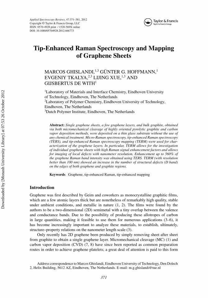
A general view of the multipurpose scanning near-field optical spectrometer NTEGRASpectra (NT-MDT, Moscow, Russia) is shown in Figure 1. The tip is positioned in oneof the two longitudinal lobes near rims of the diffraction-limited laser spot to locallyenhance the electromagnetic field beneath its apex. This system allows one to lock thetip position inside the laser spot to maintain optimum illumination conditions. A near-fieldRaman image is established by raster scanning the sample with an xy-scan stage. All Ramanspectra are recorded within a spectral range of 150–3500 cm−1. A 200-line/mm gratingprovides a spectral resolution of better than 15 cm−1. The pinhole size used with the 100×oil immersion objective was equal to 60 µm.
Mechanically cleaved graphene was obtained from HOPG ZYH supplied by NT-MDTCompany. Flakes were removed from bulk graphite piece by attaching them to a normaltransparent adhesive tape. After removing the tape, macroscopically homogeneous layers
Dow
nloa
ded
by [
Mon
ash
Uni
vers
ity L
ibra
ry]
at 0
7:53
26
Oct
ober
201
2
Mapping of Graphene Sheets 373
Figure 1. (Left) Schematic optical setup of the TERS instrument used and (right) picture of theTERS equipment. (color figure available online.)
remained attached to it. The tape was then placed in acetone for 1 h in order to release theglueing interaction between the tape and graphite sheets. Graphene sheets (10 × 10 mm2)produced via a CVD method were purchased from Graphene Laboratories (NY, USA). Thefilms were grown directly on an Ni film deposited on an oxidized silicon wafer.
A thin (0.17-mm) glass substrate, 50 × 24 mm2, was cleaned with an ulraviolet–ozonecleaning system from NovaScan Technologies, Inc. (PSD–UV, Iowa, USA) for 20 min atroom temperature to remove molecular organic contamination. Both cleaved graphene ontape and CVD graphene on nickel were carefully transferred (7) onto the cleaned glassusing a thermal release tape (Graphene Laboratories); after a quick removal of the tape,some thin graphite flakes were visible and the transparent graphene could be identified byRaman.
Results and Discussion
The two most intense Raman features for graphite are the G peak at ∼1570 cm−1 and the2D peak at ∼2680 cm−1. The G band is a tangential shear mode of carbon atoms thatcorresponds to the stretching mode in the graphite plane. The G peak is due to the doublydegenerate zone center E2g mode (14). The 2D band has nothing to do with the G peak butis a second-order process from two-zone boundary phonons. It is an intrinsic property ofgraphite and is present even in defect-free structures. Because zone-boundary phonons donot satisfy the Raman fundamental selection rule, they are not seen in first-order Ramanspectra of defect-free graphite. Such phonons give rise to a peak at ∼1350 cm−1 in graphitecontaining defects, usually called the D peak (13). With a conventional Raman spectroscopysetup, a large area of the graphite/graphene surface is analyzed at the same time and theaverage number and type of defects can be calculated. However, TERS was utilized in orderto learn more about the local defect distribution in individual graphene sheets and optimizeprocedures for their functionalization.
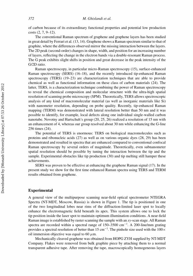
The material composition of the tip localizes and enhances the scattered optical radia-tion over the incident radiation, its geometry and the polarization state of the incident lightin the local excitation-based scheme are of greatest importance for efficient enhancements.For our experiments we used gold tips etched from a 0.2-mm gold wire in our laboratoryfollowing a procedure used by Ren et al. (31). To obtain a measure of the sharpness andquality of the resulting tip, we mapped the reflection of the laser light from the tip using
Dow
nloa
ded
by [
Mon
ash
Uni
vers
ity L
ibra
ry]
at 0
7:53
26
Oct
ober
201
2
374 M. Ghislandi et al.
Figure 2. Scanning electron microscopy and reflectivity mapping of gold tips. (color figure availableonline.)
a photomultiplier while moving the tip in two dimensions using the scanner of the shearforce head. In Figure 2 we show scanning electron microscopy images and the resultingscan of a tip. Though the scan does not necessarily show a one-to-one correspondence tothe shape of the tip, the images clearly show the nice symmetry of the tip by the detectionof diffraction rings and a tip radius below 60 nm. This indicates a resolution of around 25nm or roughly half the tip radius.
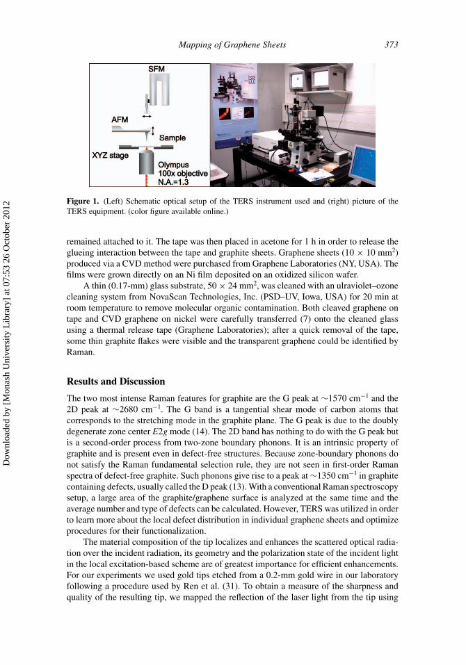
Spectroscopic imaging of mechanically cleaved (MC) graphene/graphite was obtainedby accumulation of local Raman data using TERM. Figure 3 shows an optical microscopyimage and tip-enhanced Raman topographical scans of graphite/graphene samples that weretaken with the self-made gold scanning force microscopy tip for tip-on operation mode (inthis mode the tip is close to the sample surface and active in the near field). More detailson the experiments performed can be found in Kharintsev et al. (24).
We can compare the intensity of the 2D peak region (2630–2675 cm−1) and also theshift position of these peaks. It is possible to identify clearly defined areas corresponding tographene using TERM (black dot in Figure 3, right). This is due to a better lateral resolutionpromoted by this technique (32).
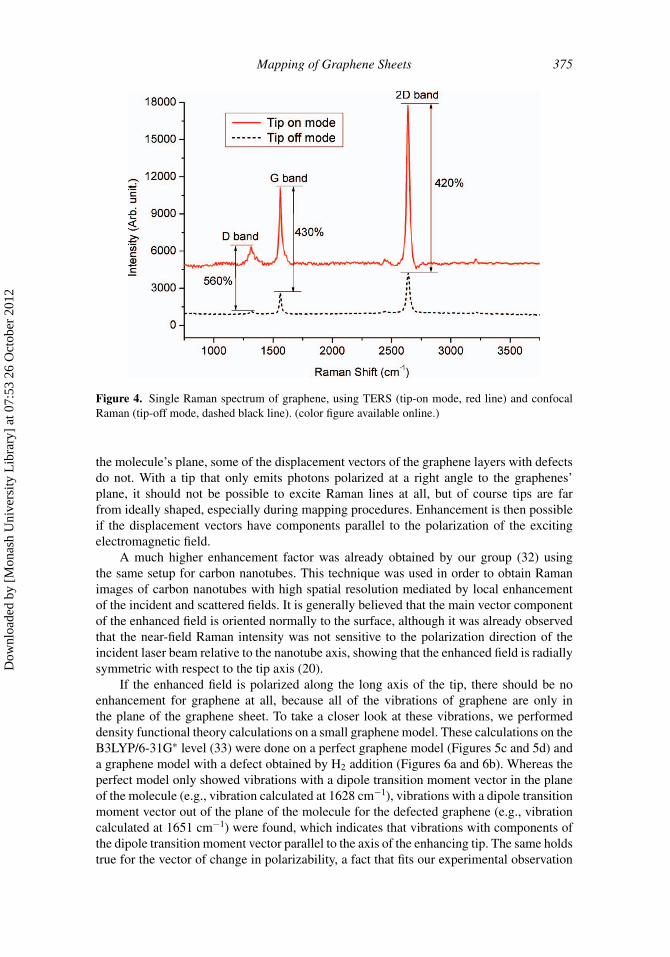
In the region where graphene was found, two single Raman spectra were acquired (10-sacquisition time), comparing tip-on mode and tip-off mode (in this mode, the SPM tip is faraway from the sample surface; Figure 4). An enhancement of more than 400% was verifiedfor the G and 2D bands and an enhancement of more than 500% was obtained for the Dband using TERS. Though the displacement vectors of the vibrations of graphene lie in
Figure 3. (Left) Optical microscopy image, (middle) tip-enhanced Raman mapping showing 2Dpeak intensity, and (right) 2D shift position. (color figure available online.)
Dow
nloa
ded
by [
Mon
ash
Uni
vers
ity L
ibra
ry]
at 0
7:53
26
Oct
ober
201
2
Mapping of Graphene Sheets 375
Figure 4. Single Raman spectrum of graphene, using TERS (tip-on mode, red line) and confocalRaman (tip-off mode, dashed black line). (color figure available online.)
the molecule’s plane, some of the displacement vectors of the graphene layers with defectsdo not. With a tip that only emits photons polarized at a right angle to the graphenes’plane, it should not be possible to excite Raman lines at all, but of course tips are farfrom ideally shaped, especially during mapping procedures. Enhancement is then possibleif the displacement vectors have components parallel to the polarization of the excitingelectromagnetic field.
A much higher enhancement factor was already obtained by our group (32) usingthe same setup for carbon nanotubes. This technique was used in order to obtain Ramanimages of carbon nanotubes with high spatial resolution mediated by local enhancementof the incident and scattered fields. It is generally believed that the main vector componentof the enhanced field is oriented normally to the surface, although it was already observedthat the near-field Raman intensity was not sensitive to the polarization direction of theincident laser beam relative to the nanotube axis, showing that the enhanced field is radiallysymmetric with respect to the tip axis (20).
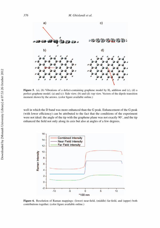
If the enhanced field is polarized along the long axis of the tip, there should be noenhancement for graphene at all, because all of the vibrations of graphene are only inthe plane of the graphene sheet. To take a closer look at these vibrations, we performeddensity functional theory calculations on a small graphene model. These calculations on theB3LYP/6-31G∗ level (33) were done on a perfect graphene model (Figures 5c and 5d) anda graphene model with a defect obtained by H2 addition (Figures 6a and 6b). Whereas theperfect model only showed vibrations with a dipole transition moment vector in the planeof the molecule (e.g., vibration calculated at 1628 cm−1), vibrations with a dipole transitionmoment vector out of the plane of the molecule for the defected graphene (e.g., vibrationcalculated at 1651 cm−1) were found, which indicates that vibrations with components ofthe dipole transition moment vector parallel to the axis of the enhancing tip. The same holdstrue for the vector of change in polarizability, a fact that fits our experimental observation
Dow
nloa
ded
by [
Mon
ash
Uni
vers
ity L
ibra
ry]
at 0
7:53
26
Oct
ober
201
2
376 M. Ghislandi et al.
Figure 5. (a), (b) Vibrations of a defect-containing graphene model by H2 addition and (c), (d) aperfect graphene model. (a) and (c): Side view; (b) and (d): top view. Vectors of the dipole transitionmoment shown by the arrows. (color figure available online.)
well in which the D band was more enhanced than the G peak. Enhancement of the G peak(with lower efficiency) can be attributed to the fact that the conditions of the experimentwere not ideal: the angle of the tip with the graphene plane was not exactly 90◦, and the tipenhanced the field not only along its axis but also at angles of a few degrees.
Figure 6. Resolution of Raman mappings: (lower) near-field, (middle) far-field, and (upper) bothcontributions together. (color figure available online.)
Dow
nloa
ded
by [
Mon
ash
Uni
vers
ity L
ibra
ry]
at 0
7:53
26
Oct
ober
201
2
Mapping of Graphene Sheets 377
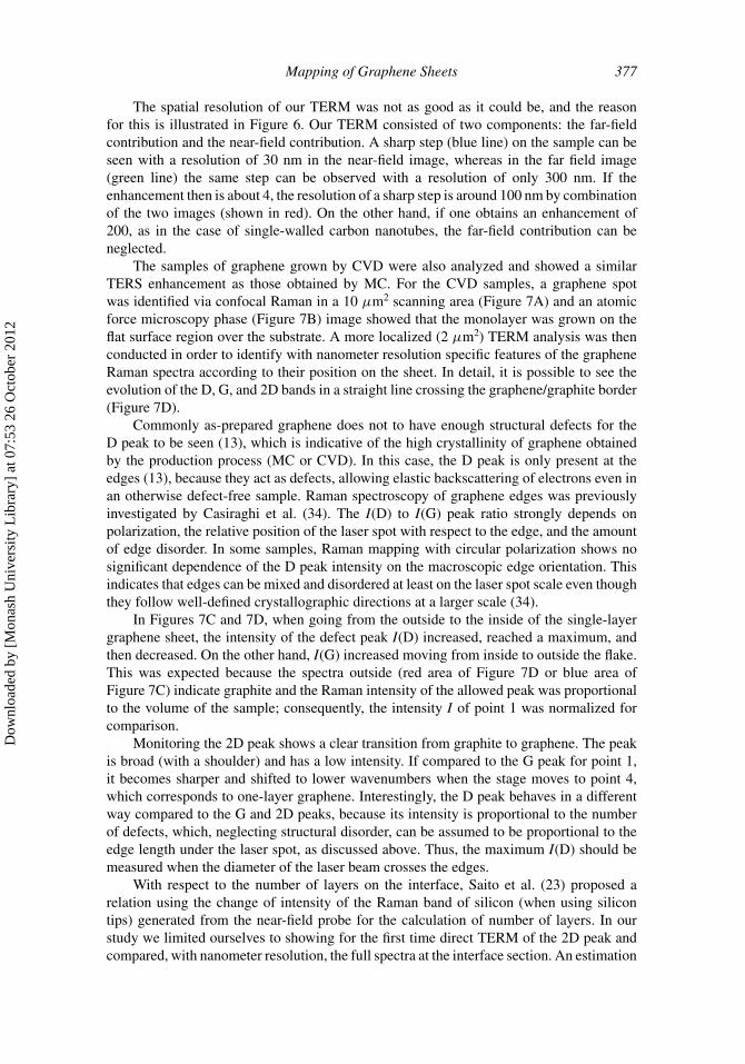
The spatial resolution of our TERM was not as good as it could be, and the reasonfor this is illustrated in Figure 6. Our TERM consisted of two components: the far-fieldcontribution and the near-field contribution. A sharp step (blue line) on the sample can beseen with a resolution of 30 nm in the near-field image, whereas in the far field image(green line) the same step can be observed with a resolution of only 300 nm. If theenhancement then is about 4, the resolution of a sharp step is around 100 nm by combinationof the two images (shown in red). On the other hand, if one obtains an enhancement of200, as in the case of single-walled carbon nanotubes, the far-field contribution can beneglected.
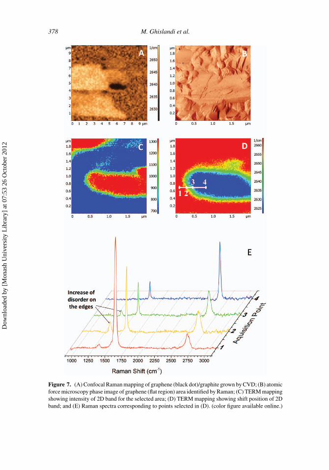
The samples of graphene grown by CVD were also analyzed and showed a similarTERS enhancement as those obtained by MC. For the CVD samples, a graphene spotwas identified via confocal Raman in a 10 µm2 scanning area (Figure 7A) and an atomicforce microscopy phase (Figure 7B) image showed that the monolayer was grown on theflat surface region over the substrate. A more localized (2 µm2) TERM analysis was thenconducted in order to identify with nanometer resolution specific features of the grapheneRaman spectra according to their position on the sheet. In detail, it is possible to see theevolution of the D, G, and 2D bands in a straight line crossing the graphene/graphite border(Figure 7D).
Commonly as-prepared graphene does not to have enough structural defects for theD peak to be seen (13), which is indicative of the high crystallinity of graphene obtainedby the production process (MC or CVD). In this case, the D peak is only present at theedges (13), because they act as defects, allowing elastic backscattering of electrons even inan otherwise defect-free sample. Raman spectroscopy of graphene edges was previouslyinvestigated by Casiraghi et al. (34). The I(D) to I(G) peak ratio strongly depends onpolarization, the relative position of the laser spot with respect to the edge, and the amountof edge disorder. In some samples, Raman mapping with circular polarization shows nosignificant dependence of the D peak intensity on the macroscopic edge orientation. Thisindicates that edges can be mixed and disordered at least on the laser spot scale even thoughthey follow well-defined crystallographic directions at a larger scale (34).
In Figures 7C and 7D, when going from the outside to the inside of the single-layergraphene sheet, the intensity of the defect peak I(D) increased, reached a maximum, andthen decreased. On the other hand, I(G) increased moving from inside to outside the flake.This was expected because the spectra outside (red area of Figure 7D or blue area ofFigure 7C) indicate graphite and the Raman intensity of the allowed peak was proportionalto the volume of the sample; consequently, the intensity I of point 1 was normalized forcomparison.
Monitoring the 2D peak shows a clear transition from graphite to graphene. The peakis broad (with a shoulder) and has a low intensity. If compared to the G peak for point 1,it becomes sharper and shifted to lower wavenumbers when the stage moves to point 4,which corresponds to one-layer graphene. Interestingly, the D peak behaves in a differentway compared to the G and 2D peaks, because its intensity is proportional to the numberof defects, which, neglecting structural disorder, can be assumed to be proportional to theedge length under the laser spot, as discussed above. Thus, the maximum I(D) should bemeasured when the diameter of the laser beam crosses the edges.
With respect to the number of layers on the interface, Saito et al. (23) proposed arelation using the change of intensity of the Raman band of silicon (when using silicontips) generated from the near-field probe for the calculation of number of layers. In ourstudy we limited ourselves to showing for the first time direct TERM of the 2D peak andcompared, with nanometer resolution, the full spectra at the interface section. An estimation
Dow
nloa
ded
by [
Mon
ash
Uni
vers
ity L
ibra
ry]
at 0
7:53
26
Oct
ober
201
2
378 M. Ghislandi et al.
Figure 7. (A) Confocal Raman mapping of graphene (black dot)/graphite grown by CVD; (B) atomicforce microscopy phase image of graphene (flat region) area identified by Raman; (C) TERM mappingshowing intensity of 2D band for the selected area; (D) TERM mapping showing shift position of 2Dband; and (E) Raman spectra corresponding to points selected in (D). (color figure available online.)
Dow
nloa
ded
by [
Mon
ash
Uni
vers
ity L
ibra
ry]
at 0
7:53
26
Oct
ober
201
2
Mapping of Graphene Sheets 379
of the higher TERS resolution using a slice through the intensity image provided spatialresolution better than 60 nm for the present experimental setup.
Conclusions
Single graphene sheets, a few graphene layers, and bulk graphite were successfully de-posited on a thin glass substrate, without the use of any chemical treatment, which can leadto contamination and damaging of the molecular structure of the specimens.
Raman spectroscopy combined with a scanning probe microscopy setup, so-calledapertureless near-field optical microscopy—in particular tip-enhanced Raman spectroscopyand mapping (TERS and TERM)—allows detection of structural defects with lateralresolution in the nanometer range. We have demonstrated for the first time direct en-hancement of more than 400% for the D, G, and 2D bands of graphene using TERS.TERM on graphite/graphene samples grown by CVD shows the different Raman prop-erties in the center and at the edges of the platelets, confirming (with resolution betterthan 100 nm) an increase in the D band on the edges of both graphene and graphiteregions.
Acknowledgments
This work is part of the Research Programme of the Dutch Polymer Institute (DPI), Eind-hoven, The Netherlands, project nos. 648 and 692. Financial support is gratefully acknowl-edged. We thank also to Jos Laven (TU/e) for help with preliminary measurements on aconventional confocal Raman spectrometer.
References
1. Novoselov, K.S., Geim, A.K., Morozov, S.V., Jiang, D., Zhang, Y., Dubonos, S.V., Grigorieva,I.V., and Firsov, A.A. (2004) Electric field effect in atomically thin carbon films. Science, 306:666–669.
2. Geim, A.K. and Novoselov, K.S. (2007) The rise of graphene. Nat. Mater., 6: 183–191.3. Castro Neto, A.H., Guinea, F., Peres, N.M.R., Novoselov, K.S., and Geim, A.K. (2009) The
electronic properties of graphene. Rev. Mod. Phys., 81: 109–162.4. Eda, G., Fanchini, G., and Chhowalla, M. (2008) Large-area ultrathin films of reduced graphene
oxide as a transparent and flexible electronic material. Nature Nanotechnology, 3: 270–274.5. Tkalya, E., Ghislandi, M., Alekseev, A., Koning, C., and Loos, J. (2010) Latex-based concept for
the preparation of graphene-based polymer nanocomposites. J. Mater. Chem., 20: 3035–3039.6. Stankovich, S., Dikin, D.A., Dommett, G.H.B., Kohlhaas, K.M., Zimney, E.J., Stach, E.A., Piner,
R.D., Nguyen, S.T., and Ruoff, R.S. (2006) Graphene-based composite materials. Nature, 442:282–286.
7. Kim, K.S., Zhao, Y., Jang, H., Lee, S.Y., Kim, J.M., Kim, K.S., Ahn, J.-H., Kim, P., Choi, J.-Y.,and Hong, B.H. (2009) Large-scale pattern growth of graphene films for stretchable transparentelectrodes. Nature, 457: 706–710.
8. Li, X., Cai, W., An, J., Kim, S., Nah, J., Yang, D., Piner, R., Velamakanni, A., Jung, I., Tutuc, E.,Banerjee, S.K., Colombo, L., and Ruoff, R.S. (2009) Large-area synthesis of high-quality anduniform graphene films on copper foils. Science, 324: 1312–1314.
9. Zhang, Y.B., Small, J.P., Pontius, W.V., and Kim, P. (2005) Fabrication and electric-field-dependent transport measurements of mesoscopic graphite devices. Appl. Phys. Lett., 86: 073104.
Dow
nloa
ded
by [
Mon
ash
Uni
vers
ity L
ibra
ry]
at 0
7:53
26
Oct
ober
201
2
380 M. Ghislandi et al.
10. Wang, X.L. (2008) Proposal for a new class of materials: Spin gapless semiconductors. Phys.Rev. Lett., 100: 156404.
11. Ramanathan, T., Abdala, A.A., Stankovich, S., Dikin, D.A., Herrera-Alonso, M., Piner, R.D.,Adamson, D.H., Schniepp, H.C., Chen, X., Ruoff, R.S., Nguyen, S.T., Aksay, I.A., Prud’homme,R.K., and Brinson, L.C. (2008) Functionalized graphene sheets for polymer nanocomposites.Nature Nanotechnology, 3: 327–331.
12. Reina, A., Jia, X.T., Ho, J., Nezich, D., Son, H.B., Bulovic, V., Dresselhaus, M.S., and Kong, J.(2009) Large area, few-layer graphene films on arbitrary substrates by chemical vapor deposition.Nano Lett., 9: 30–35.
13. Ferrari, A.C., Meyer, J.C., Scardaci, V., Casiraghi, C., Lazzeri, M., Mauri, F., Piscanec, S., Jiang,D., Novoselov, K.S., Roth, S., and Geim, A.K. (2006) Raman spectrum of graphene and graphenelayers. Phys. Rev. Lett., 97: 187401.
14. Ferrari, A.C. (2007) Raman spectroscopy of graphene and graphite: Disorder, electron–phononcoupling, doping and nonadiabatic effects. Solid State Comm., 143: 47–57.
15. Lewis, I.R. and Griffiths, P.R. (1996) Raman spectrometry with fiber-optic sampling. Appl.Spectros., 50: A12–A30.
16. Chang, R.K. and Laube, B.L. (1984) Surface-enhanced Raman-scattering and nonlinear opticsapplied to electrochemistry. CRC Crit. Rev. Solid State Mater. Sci., 12: 1–73.
17. Schedin, F., Lidorikis, E., Lombardo, A., Kravets, V.G., Geim, A.K., Grigorenko, A.N.,Novoselov, K.S., and Ferrari, A.C. (2010) Surface-enhanced Raman spectroscopy of graphene.ACS Nano, 4: 5617–5626.
18. Goncalves, G., Marques, P., Granadeiro, C.M., Nogueira, H.I.S., Singh, M.K., and Gracio, J.(2009) Surface modification of graphene nanosheets with gold nanoparticles: The role of oxygenmoieties at graphene surface on gold nucleation and growth. Chem. Mater., 21: 4796–4802.
19. Stockle, R.M., Suh, Y.D., Deckert, V., and Zenobi, R. (2000) Nanoscale chemical analysis bytip-enhanced Raman spectroscopy. Chem. Phys. Lett., 318: 131–136.
20. Hartschuh, A., Sanchez, E.J., Xie, X.S., and Novotny, L. (2003) High-resolution near-field Ramanmicroscopy of single-walled carbon nanotubes. Phys. Rev. Lett., 90: 095503.
21. Cancado, L.G., Hartschuh, A., and Novotny, L. (2009) Tip-enhanced Raman spectroscopy ofcarbon nanotubes. J. Raman Spectros., 40: 1420–1426.
22. Chan, K.L.A. and Kazarian, S.G. (2011) Tip-enhanced Raman mapping with top-illuminationAFM. Nanotechnology, 22: 175701 (5 pp.).
23. Saito, Y., Verma, P., Masui, K., Inouye, Y., and Kawata, S. (2009) Nano-scale analysis of graphenelayers by tip-enhanced near-field Raman spectroscopy. J. Raman Spectros., 40: 1434–1440.
24. Kharintsev, S.S., Hoffmann, G.G., Dorozhkin, P.S., de With, G., and Loos, J. (2007) Atomicforce and shear force based tip-enhanced Raman spectroscopy and imaging. Nanotechnology,18: 315502 (9 pp.).
25. Sanchez, E.J., Novotny, L., and Xie, X.S. (1999) Near-field fluorescence microscopy based ontwo-photon excitation with metal tips. Phys. Rev. Lett., 82: 4014–4017.
26. Novotny, L. and Stranick, S.J. (2006) Near–field optical microscopy and spectroscopy withpointed probes. Ann. Rev. Phys. Chem., 303–331.
27. Bailo, E. and Deckert, V. (2008) Tip-enhanced Raman spectroscopy of single RNA strands:Towards a novel direct-sequencing method. Angew. Chem. Int. Ed., 47: 1658–1661.
28. Pettinger, B. (2010) Single-molecule surface- and tip-enhanced Raman spectroscopy. Mol. Phys.,108: 2039–2059.
29. Zeisel, D., Dutoit, B., Deckert, V., Roth, T., and Zenobi, R. (1997) Optical spectroscopy and laserdesorption on a nanometer scale. Anal. Chem., 69: 749–754.
30. Kharintsev, S.S., Noskov, A.I., Hoffmann, G.G., and Loos, J. (2010) Near-field optical taper an-tennas fabricated with a highly replicable AC electrochemical etching method. Nanotechnology,22: 025202 (11 pp.).
31. Ren, B., Picardi, G., and Pettinger, B. (2004) Preparation of gold tips suitable for tip-enhancedRaman spectroscopy and light emission by electrochemical etching. Rev. Sci. Instrum., 75:837–841.
Dow
nloa
ded
by [
Mon
ash
Uni
vers
ity L
ibra
ry]
at 0
7:53
26
Oct
ober
201
2

Mapping of Graphene Sheets 381
32. Kharintsev, S.S., Hoffmann, G.G., Loos, J., de With, G., Dorozhkin, P.S., and Salakhov, M.K.(2007) Subwavelength-resolution near-field Raman spectroscopy. J. Exp. Theor. Phys., 105:909–915.
33. Frisch, M.J., et al (2009) Gaussian 09, Revision B.01. Gaussian, Inc.: Wallingford, CT.34. Casiraghi, C., Hartschuh, A., Qian, H., Piscanec, S., Georgi, C., Fasoli, A., Novoselov, K.S.,
Basko, D.M., and Ferrari, A.C. (2009) Raman spectroscopy of graphene edges. Nano Lett., 9:1433–1441.
Dow
nloa
ded
by [
Mon
ash
Uni
vers
ity L
ibra
ry]
at 0
7:53
26
Oct
ober
201
2