Embed Size (px)
Citation preview

Thermomechanical fatigue failure of interfaces in lead-freesoldersCitation for published version (APA):Erinc, M. E. (2007). Thermomechanical fatigue failure of interfaces in lead-free solders. Eindhoven: TechnischeUniversiteit Eindhoven. https://doi.org/10.6100/IR630785
DOI:10.6100/IR630785
Document status and date:Published: 01/01/2007
Document Version:Publisher’s PDF, also known as Version of Record (includes final page, issue and volume numbers)
Please check the document version of this publication:
• A submitted manuscript is the version of the article upon submission and before peer-review. There can beimportant differences between the submitted version and the official published version of record. Peopleinterested in the research are advised to contact the author for the final version of the publication, or visit theDOI to the publisher's website.• The final author version and the galley proof are versions of the publication after peer review.• The final published version features the final layout of the paper including the volume, issue and pagenumbers.Link to publication
General rightsCopyright and moral rights for the publications made accessible in the public portal are retained by the authors and/or other copyright ownersand it is a condition of accessing publications that users recognise and abide by the legal requirements associated with these rights.
• Users may download and print one copy of any publication from the public portal for the purpose of private study or research. • You may not further distribute the material or use it for any profit-making activity or commercial gain • You may freely distribute the URL identifying the publication in the public portal.
If the publication is distributed under the terms of Article 25fa of the Dutch Copyright Act, indicated by the “Taverne” license above, pleasefollow below link for the End User Agreement:www.tue.nl/taverne
Take down policyIf you believe that this document breaches copyright please contact us at:[email protected] details and we will investigate your claim.
Download date: 12. Apr. 2020

Thermomechanical fatigue failure of
interfaces in lead-free solders
Muge Erinc
This research was financially supported by the Dutch Technology Foundation STW(project number EWT.4924), applied science division of NWO and the technologyprogram of the Ministry of Economic Affairs of the Netherlands.
CIP-DATA LIBRARY TECHNISCHE UNIVERSITEIT EINDHOVEN
Erinc, Muge
Thermomechanical fatigue failure of interfaces in lead-free solders.
Eindhoven University of Technology, 2007.Proefschrift.
A catalogue record is available from the Eindhoven University of TechnologyLibrary. ISBN: 978-90-386-1149-5
This thesis is prepared with LATEX2ǫ
Cover design: Sjoerd Cloos
Printed by the Universiteitsdrukkerij TU Eindhoven, Eindhoven, The Netherlands.
Thermomechanical fatigue failure of
interfaces in lead-free solders
Proefschrift
ter verkrijging van de graad van doctoraan de Technische Universiteit Eindhoven,
op gezag van de Rector Magnificus, prof.dr.ir. C.J. van Duijn,voor een commissie aangewezen door het College voor Promoties
in het openbaar te verdedigen opmaandag 3 december 2007 om 16.00 uur
door
Muge Erinc
geboren te Ankara, Turkije
Dit proefschrift is goedgekeurd door de promotor:
prof.dr.ir. M.G.D. Geers
Copromotor:dr.ir. P.J.G. Schreurs
Contents
Summary vii
1 Introduction 11.1 Solders in Microelectronics . . . . . . . . . . . . . . . . . . . . . . . . . . 11.2 Objective . . . . . . . . . . . . . . . . . . . . . . . . . . . . . . . . . . . . 31.3 Outline of thesis . . . . . . . . . . . . . . . . . . . . . . . . . . . . . . . . 4
2 Microstructural Analysis of SnAgCu 52.1 Introduction . . . . . . . . . . . . . . . . . . . . . . . . . . . . . . . . . . 62.2 Experimental Procedure . . . . . . . . . . . . . . . . . . . . . . . . . . . 72.3 Results & Discussion . . . . . . . . . . . . . . . . . . . . . . . . . . . . . 9
2.3.1 Microstructure . . . . . . . . . . . . . . . . . . . . . . . . . . . . 92.3.2 Mode I and Mode II failure . . . . . . . . . . . . . . . . . . . . . 132.3.3 Micro-mechanical properties . . . . . . . . . . . . . . . . . . . . 15
2.4 Conclusions . . . . . . . . . . . . . . . . . . . . . . . . . . . . . . . . . . 18
3 Bump/pad interfacial fatigue fracture 213.1 Introduction . . . . . . . . . . . . . . . . . . . . . . . . . . . . . . . . . . 223.2 Experimental Procedure . . . . . . . . . . . . . . . . . . . . . . . . . . . 233.3 Results of fatigue tests . . . . . . . . . . . . . . . . . . . . . . . . . . . . 25
3.3.1 Failure Types . . . . . . . . . . . . . . . . . . . . . . . . . . . . . 273.3.2 Size Effect . . . . . . . . . . . . . . . . . . . . . . . . . . . . . . . 293.3.3 Fractography . . . . . . . . . . . . . . . . . . . . . . . . . . . . . 30
3.4 Cohesive Zone Model (CZM) . . . . . . . . . . . . . . . . . . . . . . . . 313.4.1 Characterization of CZM . . . . . . . . . . . . . . . . . . . . . . 323.4.2 Parameter determination . . . . . . . . . . . . . . . . . . . . . . 33
3.5 Application to SnAgCu solder interconnect . . . . . . . . . . . . . . . . 363.6 Conclusions . . . . . . . . . . . . . . . . . . . . . . . . . . . . . . . . . . 38
4 Intergranular thermal fatigue damage 394.1 Introduction . . . . . . . . . . . . . . . . . . . . . . . . . . . . . . . . . . 404.2 Experimental . . . . . . . . . . . . . . . . . . . . . . . . . . . . . . . . . 42
4.2.1 Experimental Procedure . . . . . . . . . . . . . . . . . . . . . . . 42
v
vi CONTENTS
4.2.2 Results and Discussion . . . . . . . . . . . . . . . . . . . . . . . . 444.3 Simulations . . . . . . . . . . . . . . . . . . . . . . . . . . . . . . . . . . 47
4.3.1 Parameter identification . . . . . . . . . . . . . . . . . . . . . . . 504.3.2 Sensitivity Analysis . . . . . . . . . . . . . . . . . . . . . . . . . 524.3.3 BGA solder ball simulations . . . . . . . . . . . . . . . . . . . . . 53
4.4 Conclusions . . . . . . . . . . . . . . . . . . . . . . . . . . . . . . . . . . 56
5 Microstructural modeling and fatigue life predictions 595.1 Introduction . . . . . . . . . . . . . . . . . . . . . . . . . . . . . . . . . . 605.2 Experimental Analyses . . . . . . . . . . . . . . . . . . . . . . . . . . . . 61
5.2.1 Blowholes in solder balls . . . . . . . . . . . . . . . . . . . . . . 615.2.2 Crystallography . . . . . . . . . . . . . . . . . . . . . . . . . . . . 62
5.3 Numerical Analyses . . . . . . . . . . . . . . . . . . . . . . . . . . . . . 645.3.1 Cohesive zone model . . . . . . . . . . . . . . . . . . . . . . . . . 645.3.2 The slice model . . . . . . . . . . . . . . . . . . . . . . . . . . . . 655.3.3 Fatigue life predictions . . . . . . . . . . . . . . . . . . . . . . . . 675.3.4 Validation . . . . . . . . . . . . . . . . . . . . . . . . . . . . . . . 74
5.4 Conclusions . . . . . . . . . . . . . . . . . . . . . . . . . . . . . . . . . . 75
6 Impact of miniaturization on solder reliability 776.1 Introduction . . . . . . . . . . . . . . . . . . . . . . . . . . . . . . . . . . 786.2 Simulations . . . . . . . . . . . . . . . . . . . . . . . . . . . . . . . . . . 79
6.2.1 Geometrical Considerations . . . . . . . . . . . . . . . . . . . . . 796.2.2 Microstructural Considerations . . . . . . . . . . . . . . . . . . . 82
6.3 Conclusions . . . . . . . . . . . . . . . . . . . . . . . . . . . . . . . . . . 85
7 Conclusions 87
Bibliography 91
Samenvatting 99
Acknowledgements 101
Curriculum Vitae 103
Summary
Thermomechanical fatigue failure of interfaces in lead-free solders
The European Union Waste Electrical and Electronic Equipment Directive (WEEE)and Restriction of Hazardous Substances Directive (RoHS) banned lead from elec-tronic systems from July 1, 2006 onwards, which has led to much interest in lead-free solders in the past years. Among several lead-free solder alternatives, SnAgCuis a widely accepted replacement due to its better creep-fatigue resistance and mi-crostructural stability. SnAgCu has been extensively studied in the past decade,however, there are still issues to be resolved concerning solder reliability, the un-derlying mechanisms of thermo-mechanical fatigue failure, fatigue life predictionsand the overall effect of decreasing component size, driven by the ongoing miniatur-ization trend. This thesis aims to scientifically contribute to this subject by a coupledexperimental-numerical approach.
In solder joint reliability, the bump/pad interface has a crucial role, the quality ofwhich is determined by the metallization and interfacial defects. Solder balls, sol-der paste and cast eutectic SnAgCu are reflowed on Cu, Ni/Au and Cu/Ni(V)/Aumetallization layers and the substrate influence on the bulk and interfacial met-allurgy is examined. The damage propagation at SnAgCu soldered joints on Cuand Ni/Au substrates are investigated and microstructure related damage localiza-tion is identified as the dominant failure mechanism. Therefore, continuum dam-age approaches are believed to be inadequate for solder joint reliability predictions.Nano-indentation and tensile testing is used for the mechanical characterization ofSnAgCu. An assessment on indentation parameters for solders is conducted and theinfluence of the Ag content on material properties of SnAgCu is presented.
One of the main causes of ball grid array (BGA) failure is thermo-mechanical fatiguecrack propagation in the solder, which is almost always observed at the bump/padjunction. Motivated by this fact, a combined experimental-numerical study on thecyclic mechanical response of SnAgCu/Ni-Au interface is conducted. In this study,damage evolution at the bond/pad interface is characterized by dedicated fatiguetests. Local deformations leading to crack propagation are simulated by separation
vii
viii SUMMARY
of interfaces through a cohesive zone approach. Solder joints are tested under cyclicshear and cyclic tension for different specimen sizes and strain amplitudes. Twodifferent damage mechanisms are observed: local deformations in the bulk and at thebonding interface. The interfacial failure mode is typically favored at a high initialstress, and a small solder volume. Crack propagation is simulated by an irreversiblelinear traction-separation cohesive zone law accompanied by a non-linear interfacialdamage parameter. Later, tensile and shear experiments are used to characterize thecohesive zone parameters for the normal and the tangential opening, respectively.
Interfacial fatigue damage in BGA solders is caused by the difference in coefficientof thermal expansion (CTE) of the materials in the package. Apart from this thermalincompatibility in the package, Sn based solders are themselves prone to thermalfatigue damage due to the intrinsic thermal anisotropy of the β-Sn phase. Ther-mal fatigue causes local deformations especially at the grain boundaries. Hence,the thermal fatigue response of bulk SnAgCu is investigated as well. Bulk SnAgCuspecimens are thermally cycled between -40 and 125◦C and mechanically tested af-terwards in order to quantify the thermal fatigue damage. A size dependent cyclicsoftening behavior is observed. Test specimens are individually modeled includingthe microstructure and local crystallographic orientations, on the basis of orienta-tion imaging scans (OIM). Both thermal cycling and tensile testing are imposed asboundary conditions. Reproducing the experimental results in the simulations, pa-rameters of a cohesive zone based intergranular fatigue damage model are identified.Finally, the intergranular damage law characterized in this study is combined withthe bump/pad interfacial damage law, and a 2D microstructure-incorporated fatiguelife prediction tool is established. Using this tool, it is shown that the failure mode ofa soldered joint depends extensively on its geometry.
The model presented above is extended to 3D for a more complete description ofthe problem. To provide the microstructural input, a database containing OIM scansof several SnAgCu solder balls is constructed. A missing constituent in the modelso far, interfacial defects, i.e. voids, are examined statistically using newly manu-factured BGA packages, revealing information on their size, position and frequency.Combining all the data collected, i.e. material properties, microstructure, defects,local damage laws, a 3D slice model from a BGA package is constructed. The slicemodel contains a single solder ball connecting the board and the chip. A series ofcase studies is created using experimental input such as different microstructuresand initial defects allowing a statistical analysis. Fatigue life of these models arepredicted and the results are validated by failure distribution analyses of BGA pack-ages provided by the industry. Here the critical solder ball assumption is made: if asolder ball fails, the electrical circuit of the BGA package is open, thus the packagefails. Setting a critical damage value for the interfaces accumulating fatigue damage,a good agreement with the experiments and simulations is obtained. It is seen thatmicrostructural modeling allows to predict and understand the scatter in the solderball fatigue life observed in reality.
Finally, the effect of solder ball size and geometry on interconnect reliability is dis-

SUMMARY ix
cussed on the basis of numerical analyses. For this purpose, a geometry factor anda microstructure factor is defined, and their influence on damage evolution is dis-cussed.

x SUMMARY

CHAPTER ONE
Introduction
1.1 Solders in Microelectronics
Soft solders are fusible metal alloys with a melting point up to 450◦C, used to connectmetallic surfaces, especially in the fields of electronics and plumbing. The most fre-quent application of soldering is assembling electronic components to printed circuitboards (PCBs). Today, miniaturization is the major driving force in consumer elec-tronics design and production. Efforts in decreasing component dimensions have ledto the development of ball grid array (BGA) and flip chip packages (Figure 1.1); withthe introduction of BGAs more than 1000 in/out terminals can be placed in a singleassembly. Bonding of the die to a substrate and its encapsulation is referred to as 1st
level, bonding of the mold and die to PCB is referred as 2nd level packaging. In flip-chips, no wiring is necessary because the chip is flipped over and directly connectedvia tiny solder balls (φ <100 µm) to the board. The 2nd level solder ball diameters arein the range of 300-760 µm. The pads on both the chip side and the printed circuitboard side contain thin films of lamellar metallic layers, the so-called under bumpmetallization (UBM). The purpose of the UBM is to prevent oxidation of copper andto enhance wetting of solder to the pad. In commercial packages, standard UBMthickness is in the range of 5-20 µm.
As a joining material, solder provides electrical, thermal and mechanical continuityin electronic packages. Solder balls in a microelectronic assembly are subjected todifferent types of loading:
• Thermal cycling due to repeated power switching evokes heat related phenom-ena. In connection, the mismatch in the coefficient of thermal expansion (CTE)between the package components causes cyclic mechanical strains.
• As a result of the multi-phase nature of Sn based solder alloys and the thermalanisotropy of β-Sn, internal stresses build up in the solder.
1

2 1 INTRODUCTION
Die Paddle Die Attach Epoxy
Substrate
Thermal ViasThermal PadsGround Plane
PC Board
Die
Figure 1.1: A commercial ball grid array package and its cross-section.
• Cyclic thermomechanical loading evokes creep-fatigue damage or creep rup-ture.
• Flex bending and buckling of the board induces bending moments as well asshear and tensile stresses on the solder joints.
The strains in a solder ball are dependent on the location of the ball on the BGA.The balls at corners experience the highest strains, resulting from a combination ofshear stresses and large tensile stresses, decreasing towards a neutral point at thecenter. The outer solder balls are termed as the critical balls; they exhibit a highrisk of failure compared to inner solder balls (Figure 1.2). Selection of an appropri-ate solder/substrate combination, in other words, the metallization, determines thelong-term joint reliability since failure often occurs near metallization layers.
Imposed by the European Union Waste Electrical and Electronic Equipment Di-rective (WEEE) and Restriction of Hazardous Substances Directive (RoHS), lead isbanned from electronic systems by July 1, 2006 except a limited number of specialapplications, triggering much interest in lead-free solders. Apart from the legal en-forcement, there are also a number of technological drivers emerging from the minia-turization trend:
• Miniaturization enforces the pitch size to be continuously reduced. The inter-nal liquid pressure of molten SnPb does not allow production of very smallsolder balls, because the SnPb droplet cannot solidify preserving the radius ofcurvature.
• Furthermore, smaller packages result in high current densities causing over-heating in heat-sink parts, such as the solder balls. It is well established thatSnPb is highly susceptible to heat, invoking coarsening in the eutectic lamellaewhich further leads to mixed creep-fatigue failure at the phase boundaries.
Due to the reasons stated above, lead-free solder alternatives have become an im-portant research topic for the microelectronics industry. SnAgCu was indicatedas the most promising solder in avionics and automotive applications where thesolder joints are subjected to numerous thermal cycles and mechanical vibrations,
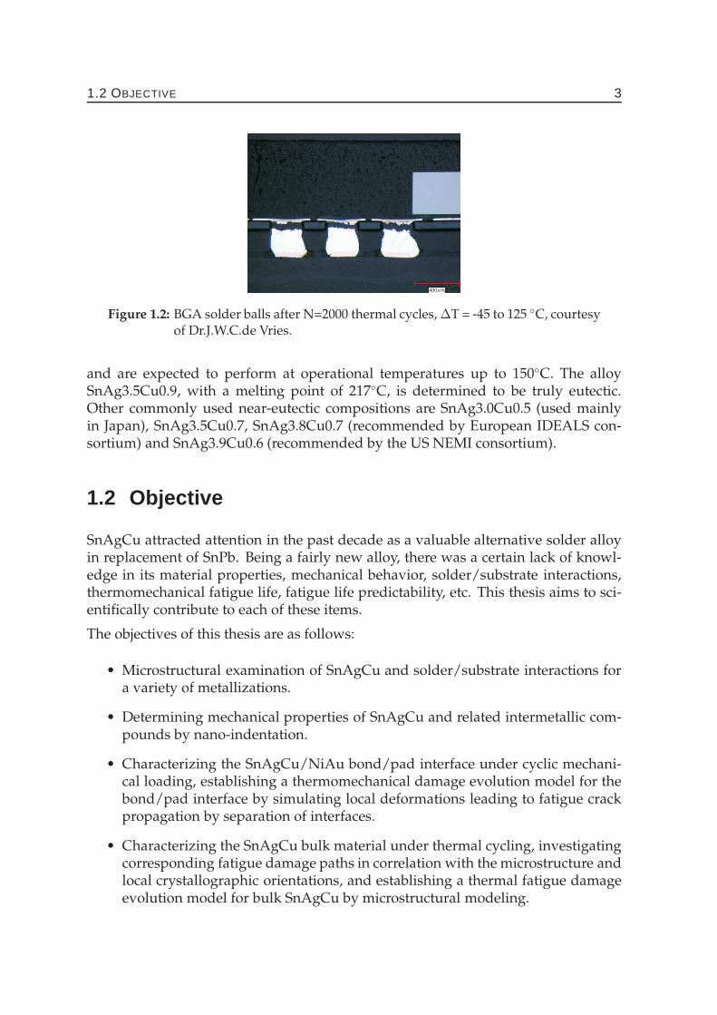
1.2 OBJECTIVE 3
400 mm
Figure 1.2: BGA solder balls after N=2000 thermal cycles, ∆T = -45 to 125 ◦C, courtesyof Dr.J.W.C.de Vries.
and are expected to perform at operational temperatures up to 150◦C. The alloySnAg3.5Cu0.9, with a melting point of 217◦C, is determined to be truly eutectic.Other commonly used near-eutectic compositions are SnAg3.0Cu0.5 (used mainlyin Japan), SnAg3.5Cu0.7, SnAg3.8Cu0.7 (recommended by European IDEALS con-sortium) and SnAg3.9Cu0.6 (recommended by the US NEMI consortium).
1.2 Objective
SnAgCu attracted attention in the past decade as a valuable alternative solder alloyin replacement of SnPb. Being a fairly new alloy, there was a certain lack of knowl-edge in its material properties, mechanical behavior, solder/substrate interactions,thermomechanical fatigue life, fatigue life predictability, etc. This thesis aims to sci-entifically contribute to each of these items.
The objectives of this thesis are as follows:
• Microstructural examination of SnAgCu and solder/substrate interactions fora variety of metallizations.
• Determining mechanical properties of SnAgCu and related intermetallic com-pounds by nano-indentation.
• Characterizing the SnAgCu/NiAu bond/pad interface under cyclic mechani-cal loading, establishing a thermomechanical damage evolution model for thebond/pad interface by simulating local deformations leading to fatigue crackpropagation by separation of interfaces.
• Characterizing the SnAgCu bulk material under thermal cycling, investigatingcorresponding fatigue damage paths in correlation with the microstructure andlocal crystallographic orientations, and establishing a thermal fatigue damageevolution model for bulk SnAgCu by microstructural modeling.
4 1 INTRODUCTION
• Developing a package size computational tool for solder joint reliability includ-ing microstructure, local crystallography and initial defects.
• Further predictions on solder joint reliability regarding solder geometry andsolder size (miniaturization).
1.3 Outline of thesis
Chapter 1 gives a brief introduction on lead-free solders in ball grid array packagesand solder fatigue.
In Chapter 2, microstructural observations on SnAgCu solder and solder/substrateinteraction are presented. Nano-indentation is used to determine the mechanicalproperties of SnAgCu. The exploitation of the nano-indentation technique for softmetals like solders is discussed.
Chapter 3 focuses on fatigue damage characterization of the bump/pad interfaceby inverse modeling. A combined experimental-numerical study on the cyclic me-chanical response of SnAgCu/Ni-Au interface is conducted. Fatigue experiments aresimulated reproducing the stress state in the specimen, from which the parametersof a cohesive zone based fatigue damage model are identified.
Chapter 4 exploits the same methods developed in Chapter 3 further, in order toinvestigate thermal fatigue in bulk SnAgCu. Here, bulk SnAgCu samples are ther-mally cycled, followed by mechanical testing to evaluate the fatigue damage. Testsamples are modeled including the original microstructure on the basis of which theexperiments are simulated. Reproducing the experimental results, parameters of acohesive zone based fatigue damage model are identified.
In Chapter 5, the numerical tools used so far are extended to 3D. The damage lawsidentified are combined and integrated in a 3D solder interconnect model. Manymodels are created using experimental input such as different microstructures andinitial defects, enabling statistical analysis. Fatigue life of these models are predictedand the results are validated using industrial failure distribution charts.
In Chapter 6, the solder ball model developed so far is extended in order to predictthe effect of solder ball size and geometry, in other words miniaturization, on inter-connect reliability on the basis of numerical analyses.
The conclusions drawn from the current study are presented in Chapter 7.
CHAPTER TWO
Microstructural Analysis of SnAgCu 1
Abstract
In solder joint reliability, the solder/pad interface plays a vital role, the quality ofwhich is determined by the metallization. In this paper, microstructural analyses ofSnAgCu alloy and soldered joints are conducted in connection with the metalliza-tion. Solder balls, solder paste and cast SnAgCu are reflowed on Cu, Ni/Au andCu/Ni(V)/Au substrates. The influence of the selected substrate on bulk and in-terfacial metallurgy, and the preferential crack propagation under tensile and shearloading is examined. It is seen that microstructural entities, i.e. intermetallic layersand primary crystals, strongly influence the crack path. Void formation is a commonproblem in BGA production, since voids degrade the mechanical properties of thesolder joint. In order to increase the joint quality, different laser reflow parametersare investigated, and an optimum procedure is established. Nano-indentation andtensile testing is used for the mechanical characterization of SnAgCu. The elasticmodulus of SnAgCu is found to increase with increasing Ag content for the consid-ered alloys. Noticing the strong influence of indentation depth, sequential loadingand peak hold time on the results obtained by nano-indentation, an assessment onthese indentation parameters for solders is conducted.
1Reproduced in part from: M. Erinc, P.J.G. Schreurs, G.Q. Zhang, M.G.D. Geers, (2005). Microstruc-tural Damage Analysis of SnAgCu Solder Joints and an Assessment on Indentation Procedures. Jour-nal of Materials Science: Materials in Electronics, 16, 93–100.
5
6 2 MICROSTRUCTURAL ANALYSIS OF SNAGCU
2.1 Introduction
Efforts in decreasing component dimensions led to the development of ball grid ar-rays (BGAs) and flip chips replacing lead-frame packages. SnAgCu is by now themost widely accepted Pb-free replacement for SnPb solder in microelectronics indus-try, due to its microstructural stability and improved creep-fatigue resistance [1, 2].BGAs can contain more than 1000 in/out terminals with solder balls of 300-760 µm indiameter. In flip-chips, galvanic deposition techniques allow for solder diameters ofas small as 35 µm. The pads on both the chip side and the printed circuit board (PCB)side contain thin films of lamellar metallic layers, the so-called under bump metal-lization (UBM), which serves as a passivation and diffusion barrier layer, as shownin Figure 2.1. Selection of an appropriate solder/UBM combination determines thelong-term joint reliability since failure often occurs along these layers. Importantcharacteristics of the metallization are the structure of the intermetallic compounds(IMCs), their morphology and thickness, mechanical properties of individual layers,adhesion between IMC layers and solder, microstructural evolution after multiplereflows and diffusion properties [3, 4]. Studies on the intermetallic compounds inSnAgCu during reflow and in the solid state can be found in [5–8].
Moulding Compound
SolderMask
Cu
Ni
Au
Solder Ball
Figure 2.1: Under bump metallization.
For Sn-rich solders, nickel based UBMs, Ni(P)/Cu, Ni(P)/Au, Ni(V)/Cu, Ni(V)/Al,etc. are commonly used. A 10-15 µm thick Ni film serves as a diffusion barrier be-tween the Cu pad and the solder, and slows down the reaction kinetics of formationof Cu6Sn5 [9, 10]. Phosphorus addition (∼9wt%) decreases the high internal stressinduced by electroless nickel deposition. With a different purpose, addition of vana-dium decreases the magnetism of nickel and speeds up the fabrication. Vanadium asan impurity in nickel is also reported to lower the Ni(V)/Cu6Sn5 interfacial energyand thereby prevents spalling into the solder [11]. Above the nickel layer, a 300 nm- 1 µm thick Au, Cu, Al or Sn film is deposited for passivation. Details of the inter-facial reaction of SnAgCu on electroless Ni(P)/Au UBM are given in [12]. Duringreflow, Ni(P) crystallizes to Ni3P and Ni3Sn4, among which Ni3P is a brittle phase. ANi(V)/Cu UBM is shown to be unstable with SnAgCu due to the spalling of inter-
2.2 EXPERIMENTAL PROCEDURE 7
metallic compounds after 20 reflows [13]. When Au is used as a passivation layer,it diffuses rapidly in SnAgCu during reflow. It is reported that the precipitation ofAuSn4, being a brittle phase, might take place in the solder after reflow [14].
In the literature, lead-free solder joint reliability is generally approached in a statis-tical manner, for which failure distribution charts are reported as typically used bythe industry. In order to reveal the underlying damage mechanisms and understandthe role of metallization on crack propagation, a more fundamental approach is re-quired. Hence, the current study focuses on a detailed analysis of the morphology ofthe bulk, and interfacial structures of SnAgCu reflowed on Cu, Ni/Au and Ni(V)/Ausubstrates, in order to establish a correlation between the interfacial microstructureand corresponding crack paths. The data collected in this study will be used later ina microstructure incorporated solder joint simulation to predict the fatigue life of thejoint. The material properties that will be used in such a simulation are here collectedusing the nano-indentation technique.
There have been several research initiatives towards determining material propertiesof solders and related intermetallic compounds by nano-indentation [15–19]. Moti-vated by the large scatter in the reported results, an assessment of indentation pro-cedures for solders is conducted. Operating parameters such as indentation depth,sequential loading and peak hold time have a strong influence on the results obtainedby nano-indentation.
Void formation is a common problem in BGA production, since voids degrade themechanical properties of the solder joint. In order to increase the joint quality, dif-ferent laser reflow parameters are investigated, and an optimum procedure is estab-lished.
2.2 Experimental Procedure
The following experimental set-ups have been made to address the present questionsat hand:
1. SnAgCu solder balls (0.3-0.76 mm in diameter) from different manufacturersand a cast SnAgCu sample were supplied. The composition of the alloys variedbetween 3.5-4.0 Ag and 0.5-0.7 Cu. The initial microstructure of the solder balls,and the cast alloy is investigated after standard metallographical preparation.
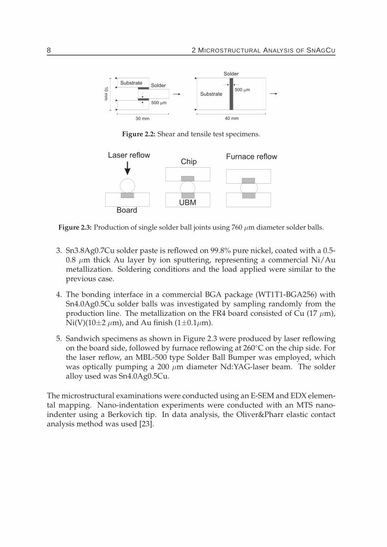
2. Sn3.8Ag0.7Cu solder paste is reflowed on commercial purity copper, repre-senting a non-UBM case. For better wetting, the cross-sections to be solderedwere polished. Specimens shown in Figure 2.2 were soldered at 260◦C on ahot plate and air cooled, and mounted to a computer controlled tensile stage.Specimens were flat and symmetric in order to minimize non-planar forces andbending moments. The load applied corresponded to a strain of 0.3-1% with astrain rate of 10−4. This strain range is concurrent with BGA flexure measure-ments [20–22].
8 2 MICROSTRUCTURAL ANALYSIS OF SNAGCU
Substrate
Substrate
Solder
Solder
30 mm
10
mm
40 mm
500 mm
500 mm
Figure 2.2: Shear and tensile test specimens.
Laser reflow Furnace reflow
Board
Chip
UBM
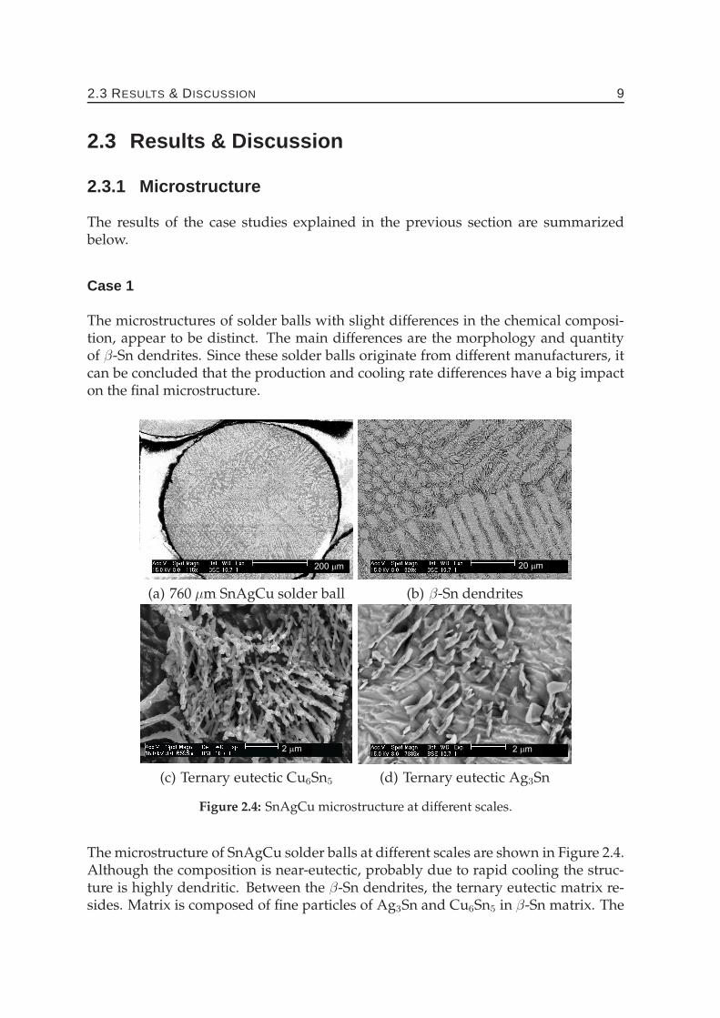
Figure 2.3: Production of single solder ball joints using 760 µm diameter solder balls.
3. Sn3.8Ag0.7Cu solder paste is reflowed on 99.8% pure nickel, coated with a 0.5-0.8 µm thick Au layer by ion sputtering, representing a commercial Ni/Aumetallization. Soldering conditions and the load applied were similar to theprevious case.
4. The bonding interface in a commercial BGA package (WT1T1-BGA256) withSn4.0Ag0.5Cu solder balls was investigated by sampling randomly from theproduction line. The metallization on the FR4 board consisted of Cu (17 µm),Ni(V)(10±2 µm), and Au finish (1±0.1µm).
5. Sandwich specimens as shown in Figure 2.3 were produced by laser reflowingon the board side, followed by furnace reflowing at 260◦C on the chip side. Forthe laser reflow, an MBL-500 type Solder Ball Bumper was employed, whichwas optically pumping a 200 µm diameter Nd:YAG-laser beam. The solderalloy used was Sn4.0Ag0.5Cu.
The microstructural examinations were conducted using an E-SEM and EDX elemen-tal mapping. Nano-indentation experiments were conducted with an MTS nano-indenter using a Berkovich tip. In data analysis, the Oliver&Pharr elastic contactanalysis method was used [23].
2.3 RESULTS & DISCUSSION 9
2.3 Results & Discussion
2.3.1 Microstructure
The results of the case studies explained in the previous section are summarizedbelow.
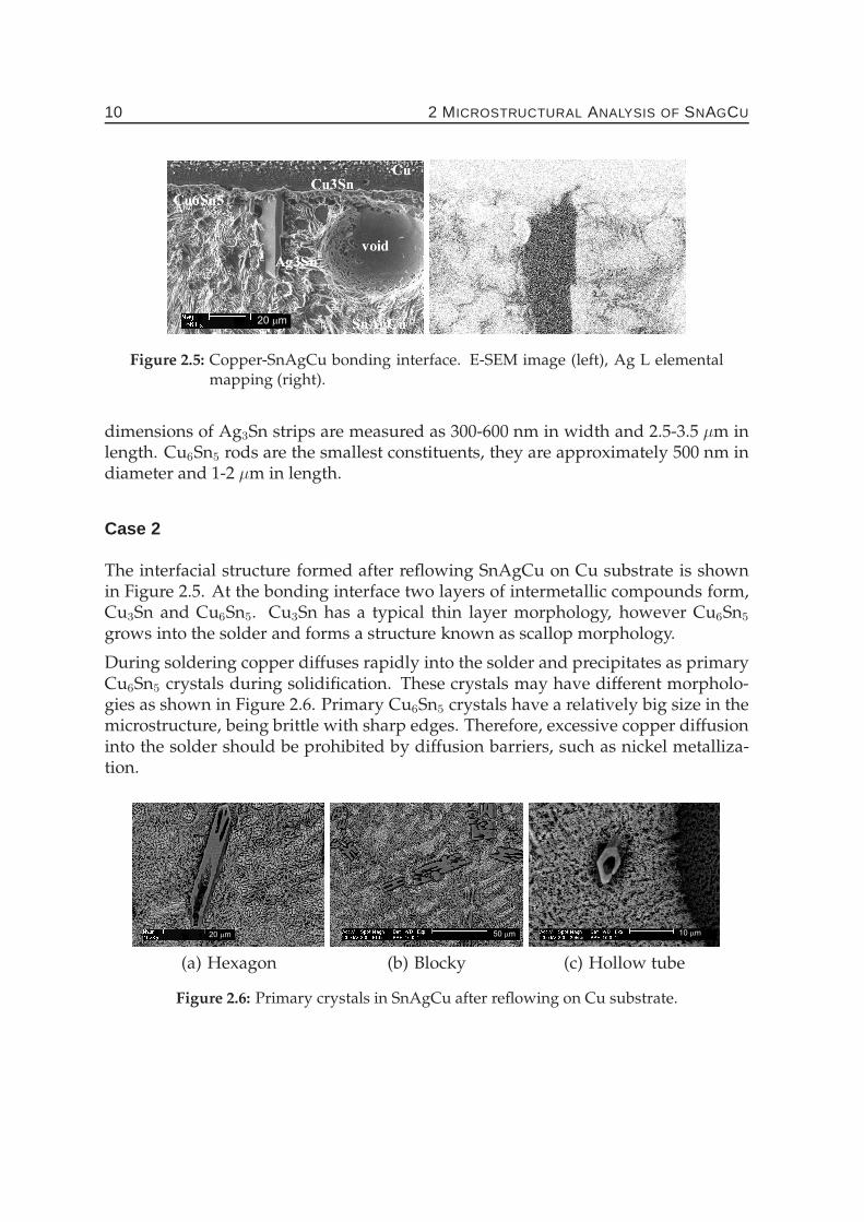
Case 1
The microstructures of solder balls with slight differences in the chemical composi-tion, appear to be distinct. The main differences are the morphology and quantityof β-Sn dendrites. Since these solder balls originate from different manufacturers, itcan be concluded that the production and cooling rate differences have a big impacton the final microstructure.
200 mm
(a) 760 µm SnAgCu solder ball
20 mm
(b) β-Sn dendrites
2 mm
(c) Ternary eutectic Cu6Sn5
2 mm
(d) Ternary eutectic Ag3Sn
Figure 2.4: SnAgCu microstructure at different scales.
The microstructure of SnAgCu solder balls at different scales are shown in Figure 2.4.Although the composition is near-eutectic, probably due to rapid cooling the struc-ture is highly dendritic. Between the β-Sn dendrites, the ternary eutectic matrix re-sides. Matrix is composed of fine particles of Ag3Sn and Cu6Sn5 in β-Sn matrix. The
10 2 MICROSTRUCTURAL ANALYSIS OF SNAGCU
20 mm
Figure 2.5: Copper-SnAgCu bonding interface. E-SEM image (left), Ag L elementalmapping (right).
dimensions of Ag3Sn strips are measured as 300-600 nm in width and 2.5-3.5 µm inlength. Cu6Sn5 rods are the smallest constituents, they are approximately 500 nm indiameter and 1-2 µm in length.
Case 2
The interfacial structure formed after reflowing SnAgCu on Cu substrate is shownin Figure 2.5. At the bonding interface two layers of intermetallic compounds form,Cu3Sn and Cu6Sn5. Cu3Sn has a typical thin layer morphology, however Cu6Sn5
grows into the solder and forms a structure known as scallop morphology.
During soldering copper diffuses rapidly into the solder and precipitates as primaryCu6Sn5 crystals during solidification. These crystals may have different morpholo-gies as shown in Figure 2.6. Primary Cu6Sn5 crystals have a relatively big size in themicrostructure, being brittle with sharp edges. Therefore, excessive copper diffusioninto the solder should be prohibited by diffusion barriers, such as nickel metalliza-tion.
20 mm
(a) Hexagon
50 mm
(b) Blocky
10 mm
(c) Hollow tube
Figure 2.6: Primary crystals in SnAgCu after reflowing on Cu substrate.
2.3 RESULTS & DISCUSSION 11
SnAgCu
Ni
Ni Sn3 4
Ni Sn3 2
10 mm
Figure 2.7: Ni/Au-SnAgCu bonding interface.
Case 3
The Ni/Au-SnAgCu interface is shown in Figure 2.7. During reflow, two transitionintermetallic layers form between Ni and SnAgCu, i.e. a 2.5-6.4 µm thick Ni3Sn2 layerand a 2-3.75 µm thick Ni3Sn4 layer. The morphology is similar to a Cu/SnAgCu in-terface, even tough Ni3Sn4 scallops are narrower and have a rough lateral surfacecompared to Cu6Sn5. It can be expected that narrow scallops provide a larger sur-face area for Ni diffusion into the solder. Near the bonding interface, primary crys-tals of Ni3Sn4 precipitate. Some of these crystals have a well-defined morphology,i.e. dipyramids, though some are idiomorphic. Since Ni acts as a diffusion barrierbetween Cu and the solder, large Cu-Sn crystals do not appear in the matrix, eventough some Cu already present in the solder still precipitates as shown in Figure 2.8.
After reflow, no Au was detectable at the bonding interface. The high diffusion rateof Au in Sn [3], together with hot-plate reflowing allows Au to diffuse longer dis-tances without segregation. Little Au (1-3%wt) was detected in the solid solutionand in the intermetallic compounds.
5 mm
(a) (Cu,Ni)6Sn5 hollow tube
5 mm
(b) Ni3Sn4 pyramid
Figure 2.8: Primary crystals in SnAgCu after reflowing on Ni substrate.
12 2 MICROSTRUCTURAL ANALYSIS OF SNAGCU
Case 4
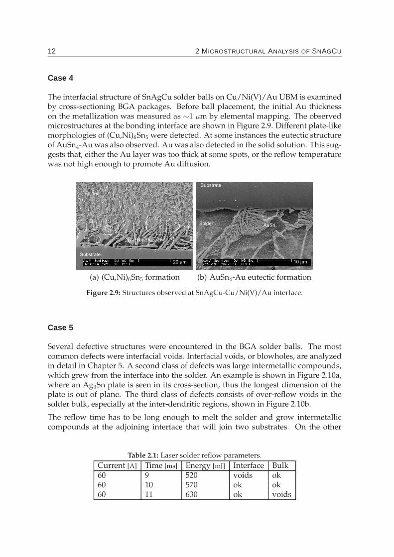
The interfacial structure of SnAgCu solder balls on Cu/Ni(V)/Au UBM is examinedby cross-sectioning BGA packages. Before ball placement, the initial Au thicknesson the metallization was measured as ∼1 µm by elemental mapping. The observedmicrostructures at the bonding interface are shown in Figure 2.9. Different plate-likemorphologies of (Cu,Ni)6Sn5 were detected. At some instances the eutectic structureof AuSn4-Au was also observed. Au was also detected in the solid solution. This sug-gests that, either the Au layer was too thick at some spots, or the reflow temperaturewas not high enough to promote Au diffusion.
Substrate
Solder
(Cu,Ni) Sn6 5
20 mm
(a) (Cu,Ni)6Sn5 formation
SnAgCu
Ni
Ni Sn3 4
Ni Sn3 2
Substrate
Solder AuSn4
10 mm
(b) AuSn4-Au eutectic formation
Figure 2.9: Structures observed at SnAgCu-Cu/Ni(V)/Au interface.
Case 5
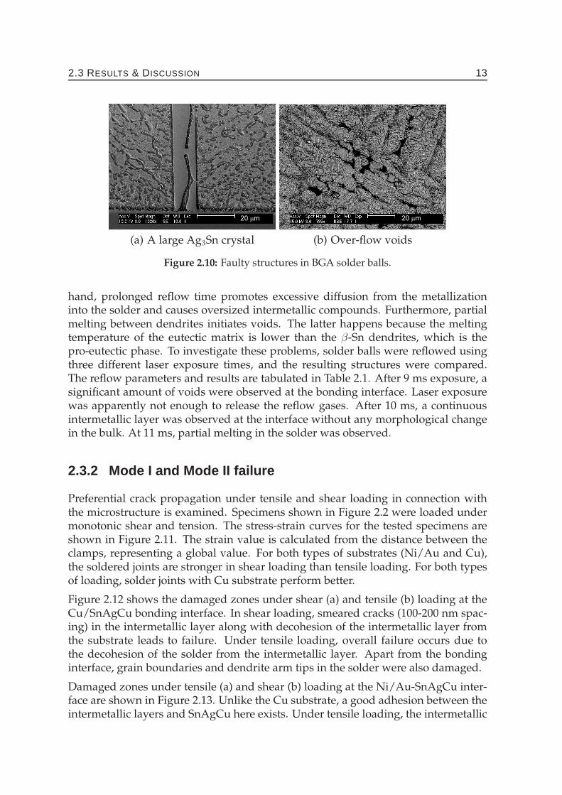
Several defective structures were encountered in the BGA solder balls. The mostcommon defects were interfacial voids. Interfacial voids, or blowholes, are analyzedin detail in Chapter 5. A second class of defects was large intermetallic compounds,which grew from the interface into the solder. An example is shown in Figure 2.10a,where an Ag3Sn plate is seen in its cross-section, thus the longest dimension of theplate is out of plane. The third class of defects consists of over-reflow voids in thesolder bulk, especially at the inter-dendritic regions, shown in Figure 2.10b.
The reflow time has to be long enough to melt the solder and grow intermetalliccompounds at the adjoining interface that will join two substrates. On the other
Table 2.1: Laser solder reflow parameters.
Current [A] Time [ms] Energy [mJ] Interface Bulk60 9 520 voids ok60 10 570 ok ok60 11 630 ok voids
2.3 RESULTS & DISCUSSION 13
20 mm
(a) A large Ag3Sn crystal
20 mm
(b) Over-flow voids
Figure 2.10: Faulty structures in BGA solder balls.
hand, prolonged reflow time promotes excessive diffusion from the metallizationinto the solder and causes oversized intermetallic compounds. Furthermore, partialmelting between dendrites initiates voids. The latter happens because the meltingtemperature of the eutectic matrix is lower than the β-Sn dendrites, which is thepro-eutectic phase. To investigate these problems, solder balls were reflowed usingthree different laser exposure times, and the resulting structures were compared.The reflow parameters and results are tabulated in Table 2.1. After 9 ms exposure, asignificant amount of voids were observed at the bonding interface. Laser exposurewas apparently not enough to release the reflow gases. After 10 ms, a continuousintermetallic layer was observed at the interface without any morphological changein the bulk. At 11 ms, partial melting in the solder was observed.
2.3.2 Mode I and Mode II failure
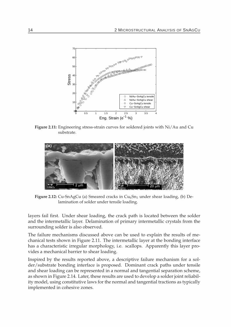
Preferential crack propagation under tensile and shear loading in connection withthe microstructure is examined. Specimens shown in Figure 2.2 were loaded undermonotonic shear and tension. The stress-strain curves for the tested specimens areshown in Figure 2.11. The strain value is calculated from the distance between theclamps, representing a global value. For both types of substrates (Ni/Au and Cu),the soldered joints are stronger in shear loading than tensile loading. For both typesof loading, solder joints with Cu substrate perform better.
Figure 2.12 shows the damaged zones under shear (a) and tensile (b) loading at theCu/SnAgCu bonding interface. In shear loading, smeared cracks (100-200 nm spac-ing) in the intermetallic layer along with decohesion of the intermetallic layer fromthe substrate leads to failure. Under tensile loading, overall failure occurs due tothe decohesion of the solder from the intermetallic layer. Apart from the bondinginterface, grain boundaries and dendrite arm tips in the solder were also damaged.
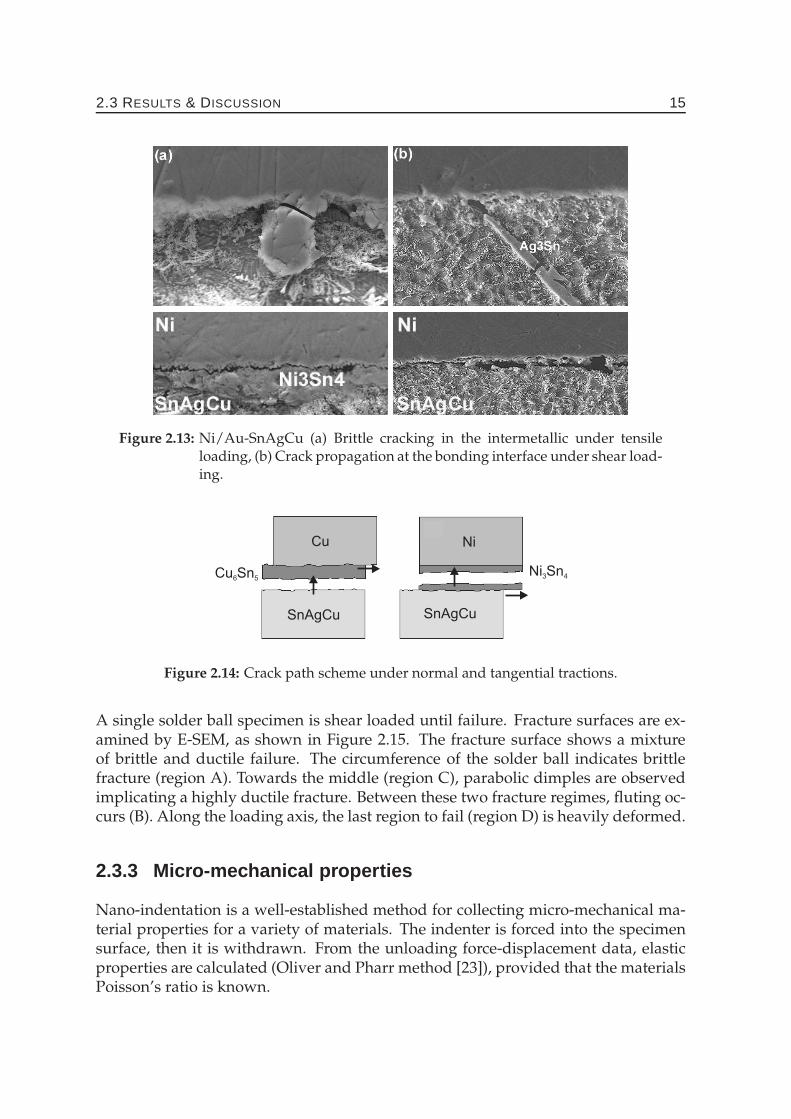
Damaged zones under tensile (a) and shear (b) loading at the Ni/Au-SnAgCu inter-face are shown in Figure 2.13. Unlike the Cu substrate, a good adhesion between theintermetallic layers and SnAgCu here exists. Under tensile loading, the intermetallic
14 2 MICROSTRUCTURAL ANALYSIS OF SNAGCU
0 0.5 1 1.5 2 2.5 3 3.5 40
10
20
30
40
50
60
70
Eng. Strain (e−1 %)
Str
ess
Ni/Au−SnAgCu tensileNi/Au−SnAgCu shearCu−SnAgCu tensileCu−SnAgCu shear
Figure 2.11: Engineering stress-strain curves for soldered joints with Ni/Au and Cusubstrate.
2 mm 20 mm
Figure 2.12: Cu-SnAgCu (a) Smeared cracks in Cu6Sn5 under shear loading, (b) De-lamination of solder under tensile loading.
layers fail first. Under shear loading, the crack path is located between the solderand the intermetallic layer. Delamination of primary intermetallic crystals from thesurrounding solder is also observed.
The failure mechanisms discussed above can be used to explain the results of me-chanical tests shown in Figure 2.11. The intermetallic layer at the bonding interfacehas a characteristic irregular morphology, i.e. scallops. Apparently this layer pro-vides a mechanical barrier to shear loading.
Inspired by the results reported above, a descriptive failure mechanism for a sol-der/substrate bonding interface is proposed. Dominant crack paths under tensileand shear loading can be represented in a normal and tangential separation scheme,as shown in Figure 2.14. Later, these results are used to develop a solder joint reliabil-ity model, using constitutive laws for the normal and tangential tractions as typicallyimplemented in cohesive zones.
2.3 RESULTS & DISCUSSION 15
Figure 2.13: Ni/Au-SnAgCu (a) Brittle cracking in the intermetallic under tensileloading, (b) Crack propagation at the bonding interface under shear load-ing.
Cu
SnAgCu SnAgCu
Cu Sn6 5
Ni
Ni Sn3 4
Figure 2.14: Crack path scheme under normal and tangential tractions.
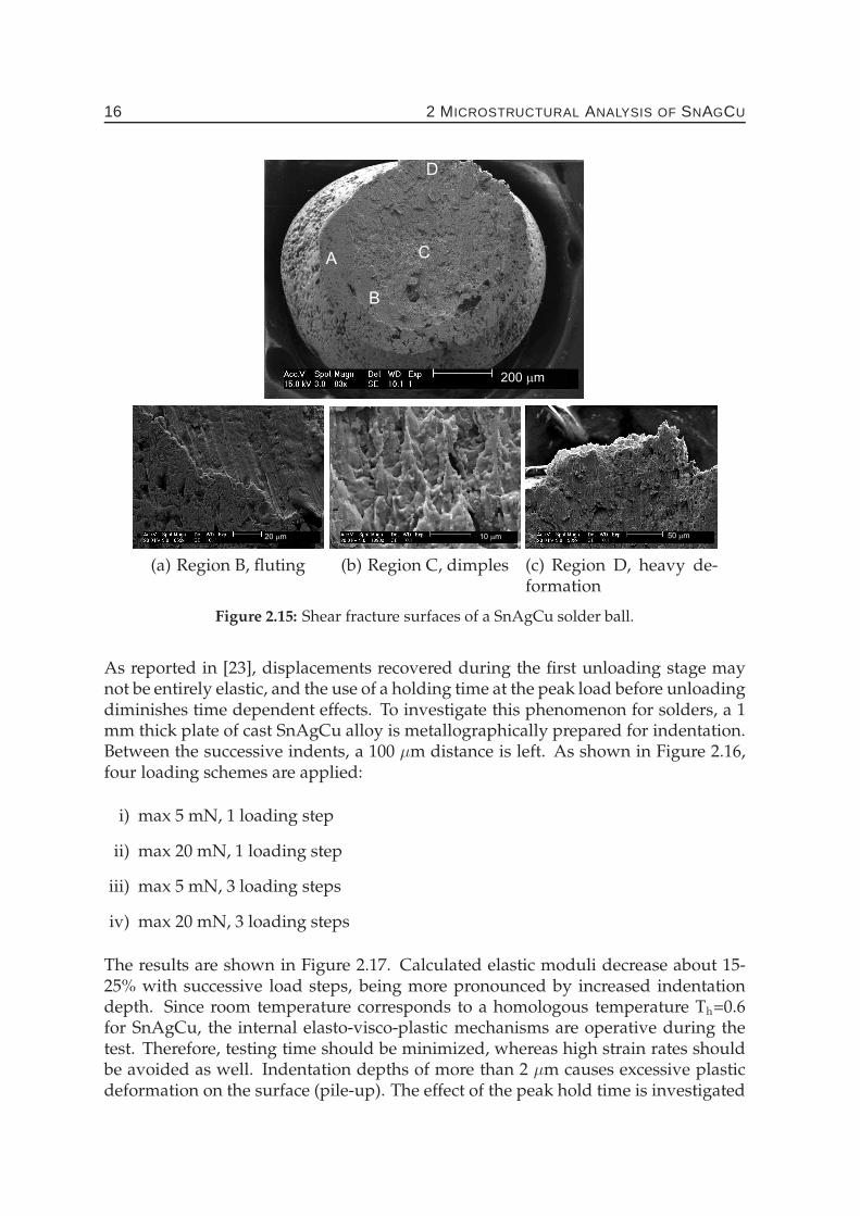
A single solder ball specimen is shear loaded until failure. Fracture surfaces are ex-amined by E-SEM, as shown in Figure 2.15. The fracture surface shows a mixtureof brittle and ductile failure. The circumference of the solder ball indicates brittlefracture (region A). Towards the middle (region C), parabolic dimples are observedimplicating a highly ductile fracture. Between these two fracture regimes, fluting oc-curs (B). Along the loading axis, the last region to fail (region D) is heavily deformed.
2.3.3 Micro-mechanical properties
Nano-indentation is a well-established method for collecting micro-mechanical ma-terial properties for a variety of materials. The indenter is forced into the specimensurface, then it is withdrawn. From the unloading force-displacement data, elasticproperties are calculated (Oliver and Pharr method [23]), provided that the materialsPoisson’s ratio is known.
16 2 MICROSTRUCTURAL ANALYSIS OF SNAGCU
A
B
C
D
200 mm
20 mm
(a) Region B, fluting
10 mm
(b) Region C, dimples
50 mm
(c) Region D, heavy de-formation
Figure 2.15: Shear fracture surfaces of a SnAgCu solder ball.
As reported in [23], displacements recovered during the first unloading stage maynot be entirely elastic, and the use of a holding time at the peak load before unloadingdiminishes time dependent effects. To investigate this phenomenon for solders, a 1mm thick plate of cast SnAgCu alloy is metallographically prepared for indentation.Between the successive indents, a 100 µm distance is left. As shown in Figure 2.16,four loading schemes are applied:
i) max 5 mN, 1 loading step
ii) max 20 mN, 1 loading step
iii) max 5 mN, 3 loading steps
iv) max 20 mN, 3 loading steps
The results are shown in Figure 2.17. Calculated elastic moduli decrease about 15-25% with successive load steps, being more pronounced by increased indentationdepth. Since room temperature corresponds to a homologous temperature Th=0.6for SnAgCu, the internal elasto-visco-plastic mechanisms are operative during thetest. Therefore, testing time should be minimized, whereas high strain rates shouldbe avoided as well. Indentation depths of more than 2 µm causes excessive plasticdeformation on the surface (pile-up). The effect of the peak hold time is investigated
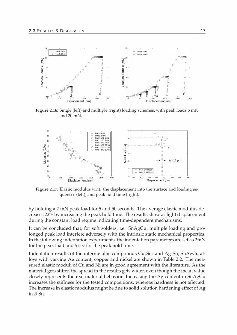
2.3 RESULTS & DISCUSSION 17
0 500 1000 1500 2000 25000
5
10
15
20
25
Displacement [nm]
Load
on
Sam
ple
[mN
]
load1 5mNload1 20mN
0 500 1000 1500 2000 25000
5
10
15
20
25
Displacement [nm]
Load
on
Sam
ple
[mN
]
load1 5mNload1 20mN
Figure 2.16: Single (left) and multiple (right) loading schemes, with peak loads 5 mNand 20 mN.
0 500 1000 1500 2000 2500 300015
20
25
30
35
40
45
50
55
60
Displacement [nm]
Mod
ulus
[GP
a]
load1 5mNload1 20mNload 1 of 3 5mNload 2 of 3 5mNload 3 of 3 5mNload 1 of 3 20mNload 2 of 3 20mNload 3 of 3 20mN
300 400 500 600 700 800 900 10000
10
20
30
40
50
60
Displacement [nm]
Mod
ulus
[GP
a]
∆ =16 µm
load1 2mN 5secload1 2mN 50sec
Figure 2.17: Elastic modulus w.r.t. the displacement into the surface and loading se-quences (left), and peak hold time (right).
by holding a 2 mN peak load for 5 and 50 seconds. The average elastic modulus de-creases 22% by increasing the peak hold time. The results show a slight displacementduring the constant load regime indicating time-dependent mechanisms.
It can be concluded that, for soft solders, i.e. SnAgCu, multiple loading and pro-longed peak load interfere adversely with the intrinsic static mechanical properties.In the following indentation experiments, the indentation parameters are set as 2mNfor the peak load and 5 sec for the peak hold time.
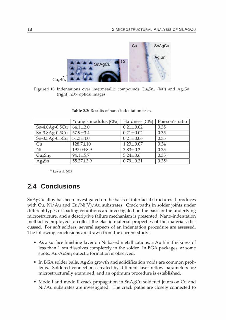
Indentation results of the intermetallic compounds Cu6Sn5 and Ag3Sn, SnAgCu al-loys with varying Ag content, copper and nickel are shown in Table 2.2. The mea-sured elastic moduli of Cu and Ni are in good agreement with the literature. As thematerial gets stiffer, the spread in the results gets wider, even though the mean valueclosely represents the real material behavior. Increasing the Ag content in SnAgCuincreases the stiffness for the tested compositions, whereas hardness is not affected.The increase in elastic modulus might be due to solid solution hardening effect of Agin β-Sn.
18 2 MICROSTRUCTURAL ANALYSIS OF SNAGCU
CuSnAgCu
Cu Sn6 5
SnAgCuCu
Ag Sn3
Figure 2.18: Indentations over intermetallic compounds Cu6Sn5 (left) and Ag3Sn(right), 20× optical images.
Table 2.2: Results of nano-indentation tests.
Young’s modulus [GPa] Hardness [GPa] Poisson’s ratioSn-4.0Ag-0.5Cu 64.1±2.0 0.21±0.02 0.35Sn-3.8Ag-0.5Cu 57.9±3.4 0.21±0.02 0.35Sn-3.5Ag-0.5Cu 51.3±4.0 0.21±0.06 0.35Cu 128.7±10 1.23±0.07 0.34Ni 197.0±8.9 3.83±0.2 0.35Cu6Sn5 94.1±5.7 5.24±0.6 0.35a
Ag3Sn 55.27±3.9 0.79±0.21 0.35a
aLee et al. 2003
2.4 Conclusions
SnAgCu alloy has been investigated on the basis of interfacial structures it produceswith Cu, Ni/Au and Cu/Ni(V)/Au substrates. Crack paths in solder joints underdifferent types of loading conditions are investigated on the basis of the underlyingmicrostructure, and a descriptive failure mechanism is presented. Nano-indentationmethod is employed to collect the elastic material properties of the materials dis-cussed. For soft solders, several aspects of an indentation procedure are assessed.The following conclusions are drawn from the current study:
• As a surface finishing layer on Ni based metallizations, a Au film thickness ofless than 1 µm dissolves completely in the solder. In BGA packages, at somespots, Au-AuSn4 eutectic formation is observed.
• In BGA solder balls, Ag3Sn growth and solidification voids are common prob-lems. Soldered connections created by different laser reflow parameters aremicrostructurally examined, and an optimum procedure is established.
• Mode I and mode II crack propagation in SnAgCu soldered joints on Cu andNi/Au substrates are investigated. The crack paths are closely connected to
2.4 CONCLUSIONS 19
the underlying microstructure. Therefore, continuum damage approaches arebelieved to be inadequate for solder joint reliability predictions.
• For soft metals (or alloys) like Sn based solders, a strong influence of in-dentation parameters on the measured material properties is observed. ForSnAgCu solder, an indentation depth of more than 500nm, and sequential load-ing schemes cause an underestimate in the elastic material properties due totemperature effects. Prolonging the peak hold time evokes time-dependent in-ternal mechanisms.
• The Ag content has a direct effect on the elastic modulus of SnAgCu alloys.For a 3.5-3.8 and 4.0 Ag content, the elastic modulus is found to increase withincreasing Ag content. This phenomenon is believed to be due to the dispersionhardening effect of Ag3Sn or solid solution hardening of (Ag).

CHAPTER THREE
Bump/pad interfacial fatigue fracture 1
Abstract
In ball grid array (BGA) packages, solder balls are exposed to cyclic thermome-chanical strains arising from the thermal mismatch between package components.Thermo-mechanical fatigue crack propagation in solder balls is almost always ob-served at the chip side of the bump/pad junction. The objective of the experimentalpart of this study is to characterize the bump/pad interface under fatigue loading.Fatigue specimens are prepared by reflowing Sn3.8Ag0.5Cu lead-free solder alloy onNi/Au substrates. Obtained results show that fatigue damage evolution stronglydepends on the microstructure. Applied strain and solder volume both have an in-fluence on the fatigue damage mechanism. In the numerical part of the study, fa-tigue experiments are modeled using the finite element technique. A cohesive zoneapproach is used to predict the fatigue damage evolution in soldered connections.Crack propagation is simulated by an irreversible linear traction-separation cohesivezone law accompanied by a non-linear damage parameter. Cohesive zone elementsare placed where failure is experimentally observed. Damage evolution parametersfor normal and tangential interaction are scrutinized through dedicated fatigue testsin pure tensile and shear directions. The proposed cohesive zone model is quanti-tatively capable of describing fatigue failure in soldered joints, which can be furtherextended to a numerical life-time prediction tool in microelectronic packages.
1Reproduced from: M. Erinc, P.J.G. Schreurs, M.G.D. Geers (2007). Integrated numerical-experimental analysis of interfacial fatigue fracture in SnAgCu solder joints. International Journal ofSolids and Structures, 44, 5680–5694.
21
22 3 BUMP/PAD INTERFACIAL FATIGUE FRACTURE
3.1 Introduction
Miniaturization trend in microelectronics has recently led to the development of ballgrid array (BGA) and flip-chip packages. As size gets smaller, local operating tem-peratures increase, hence the package components are exposed to higher mechanicalstrains. In service use, thermal expansion coefficient mismatch between the packagecomponents leads to cyclic thermomechanical strains. In a microelectronic package,solder balls are prone to thermomechanical fatigue failure (Figure 1.2), which re-sults in an open circuit and causes the electronic device to stop functioning. Anotherconsequence of miniaturization is that in small parts mechanical properties becomeinhomogeneous due to size effects. It is previously reported that size effect causesmicrostructurally driven damage localization in lead-free solders [24]. Therefore,an in-depth study relating microstructure and fatigue damage evolution is crucialfor the physical understanding of the thermomechanical fatigue problem in solderjoints.
From July 2006 on, lead (Pb) containing parts are not used in microelectronic pack-ages due to legislation. Among lead-free alternatives SnAgCu is a widely acceptedlead-free replacement due to its better creep-fatigue resistance and microstructuralstability. A broad review on lead-free solders in microelectronics is available in theliterature [3]. Microstructural evolution in annealed cast SnAgCu alloy is reportedin [1]. In their study, eutectic intermetallic components were found to coarsen, how-ever the rate of reaction was significantly slower than in SnPb solder. On bond pads,Ni/Au is the most widely used surface finish. Interfacial structure between SnAgCuand Ni/Au metallization has been extensively studied [6, 14, 25–27]. Solders are ex-posed to high homologous temperatures in service, therefore, in microstructural andmechanical characterization, evaluation of time-dependent properties becomes cru-cial. Time dependent material behavior of SnAgCu in connection with microstruc-ture is studied in detail [28–31]. A review on solder joint fatigue models is givenin [32]. However, experimental validation of these models at the level of a singlesolder interconnect is hardly existing in the literature. A chip size experimental andnumerical study of SnPb solder fatigue fracture is carried out in [33].
Fatigue life predictions for solder joints are generally carried out by using a Coffin-Manson rule or a similar empirical relationship, where the solder material is treatedas a homogenous continuum. Driven by miniaturization, solder joints have becomeso small that the size of microstructural entities in the solder is comparable to that ofthe joint itself. In order to predict fatigue failure at these size scales, rather than scaleindependent continuum-based approaches, local damage formulations in the solderjoint are needed.
The objectives of this study are:
(i) to establish a link between microstructure and damage in lead-free solder jointsunder cyclic mechanical loading,
(ii) to characterize fatigue damage evolution at the bond/pad interface and
3.2 EXPERIMENTAL PROCEDURE 23
(iii) to simulate local deformations leading to fatigue crack propagation by separa-tion of interfaces.
As motivated above, eutectic SnAgCu is here selected as the lead-free solder alloyof interest, and Ni/Au as the substrate in order to incorporate the full metallurgyat the bump/pad interface. In commercial packages, Ni is used as a diffusion bar-rier between Cu and solder, therefore Cu is not needed in the test specimens. It hasbeen previously shown by the authors that the crack path between Ni/Au substrateand SnAgCu follows physical boundaries in the microstructure (interfaces) and thecrack propagation can be split into normal and tangential components [26]. Such aninterfacial failure scheme can be modeled effectively with a cohesive zone approach.In the cohesive zone formulation used in this study, normal and tangential tractionsare decoupled. Therefore, two sets of experiments are set up; specimens that willinduce pure tensile loading at the solder/metallization interface, and specimens thatwill induce pure shear loading at the solder/metallization interface. Later, tensileexperiments are used to characterize the cohesive zone parameters for normal open-ing, and shear experiments are used to characterize the cohesive zone parameters fortangential opening.
Ni/Au-SnAgCu fatigue specimens are cyclically loaded with constant amplitude.Fatigue life is determined by the decrease in the reaction force. Experimental pro-cedures and the results of fatigue tests are explained in Section 3.2 and Section 3.3,respectively. For every fatigue test sample, the stress-strain data as a function ofnumber of cycles is plotted. Individual fatigue test samples are modeled using thefinite element technique. Cohesive zone elements are placed at the regions wherefailure is observed. In Section 3.4, the cohesive zone model used in this study andthe details of inverse parameter estimation is discussed. Last, in Section 3.5, a sol-der ball is modeled in 2D, and the fatigue life is predicted using the methodologydiscussed so far.
3.2 Experimental Procedure
First, mechanical properties of the materials that are going to be used in fatiguetests are measured. For this purpose, two half tensile parts are soldered withSn3.8Ag0.5Cu. In order to be able to measure the Young’s modulus for soft mate-rials like solders, very small strains should be measured with high accuracy. Con-tact strain measuring techniques at these small scales may induce undesired effects,i.e. sliding of extenso-meter legs, holes for extenso-meter pins. For this reason, anon-contact optical strain mapping method is used. The specimen is first sprayedto create a fine distribution of black dots on white background. The tensile test iscarried out in-situ under an optical microscope and high resolution digital imagesare acquired periodically by a digital camera. These images are then uploaded tostrain mapping software [34] where local strains are calculated by masking the sub-strate. The soldered joint was 200 µm thick and 10 mm long. Since image acquisition
24 3 BUMP/PAD INTERFACIAL FATIGUE FRACTURE
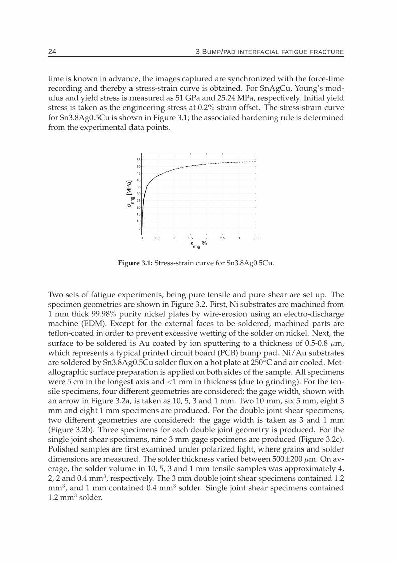
time is known in advance, the images captured are synchronized with the force-timerecording and thereby a stress-strain curve is obtained. For SnAgCu, Young’s mod-ulus and yield stress is measured as 51 GPa and 25.24 MPa, respectively. Initial yieldstress is taken as the engineering stress at 0.2% strain offset. The stress-strain curvefor Sn3.8Ag0.5Cu is shown in Figure 3.1; the associated hardening rule is determinedfrom the experimental data points.
0 0.5 1 1.5 2 2.5 3 3.5
5
10
15
20
25
30
35
40
45
50
55
εeng
%
σ eng [M
Pa]
Figure 3.1: Stress-strain curve for Sn3.8Ag0.5Cu.
Two sets of fatigue experiments, being pure tensile and pure shear are set up. Thespecimen geometries are shown in Figure 3.2. First, Ni substrates are machined from1 mm thick 99.98% purity nickel plates by wire-erosion using an electro-dischargemachine (EDM). Except for the external faces to be soldered, machined parts areteflon-coated in order to prevent excessive wetting of the solder on nickel. Next, thesurface to be soldered is Au coated by ion sputtering to a thickness of 0.5-0.8 µm,which represents a typical printed circuit board (PCB) bump pad. Ni/Au substratesare soldered by Sn3.8Ag0.5Cu solder flux on a hot plate at 250◦C and air cooled. Met-allographic surface preparation is applied on both sides of the sample. All specimenswere 5 cm in the longest axis and <1 mm in thickness (due to grinding). For the ten-sile specimens, four different geometries are considered; the gage width, shown withan arrow in Figure 3.2a, is taken as 10, 5, 3 and 1 mm. Two 10 mm, six 5 mm, eight 3mm and eight 1 mm specimens are produced. For the double joint shear specimens,two different geometries are considered: the gage width is taken as 3 and 1 mm(Figure 3.2b). Three specimens for each double joint geometry is produced. For thesingle joint shear specimens, nine 3 mm gage specimens are produced (Figure 3.2c).Polished samples are first examined under polarized light, where grains and solderdimensions are measured. The solder thickness varied between 500±200 µm. On av-erage, the solder volume in 10, 5, 3 and 1 mm tensile samples was approximately 4,2, 2 and 0.4 mm3, respectively. The 3 mm double joint shear specimens contained 1.2mm3, and 1 mm contained 0.4 mm3 solder. Single joint shear specimens contained1.2 mm3 solder.
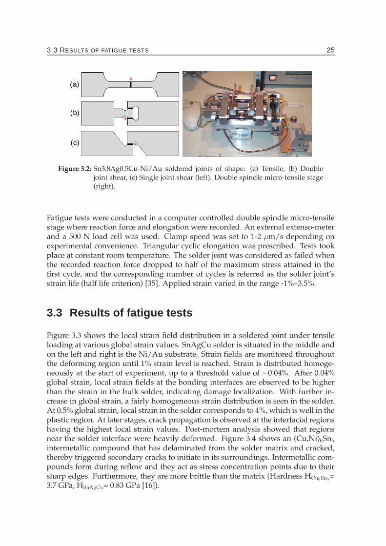
3.3 RESULTS OF FATIGUE TESTS 25
Figure 3.2: Sn3.8Ag0.5Cu-Ni/Au soldered joints of shape: (a) Tensile, (b) Doublejoint shear, (c) Single joint shear (left). Double spindle micro-tensile stage(right).
Fatigue tests were conducted in a computer controlled double spindle micro-tensilestage where reaction force and elongation were recorded. An external extenso-meterand a 500 N load cell was used. Clamp speed was set to 1-2 µm/s depending onexperimental convenience. Triangular cyclic elongation was prescribed. Tests tookplace at constant room temperature. The solder joint was considered as failed whenthe recorded reaction force dropped to half of the maximum stress attained in thefirst cycle, and the corresponding number of cycles is referred as the solder joint’sstrain life (half life criterion) [35]. Applied strain varied in the range -1%–3.5%.
3.3 Results of fatigue tests
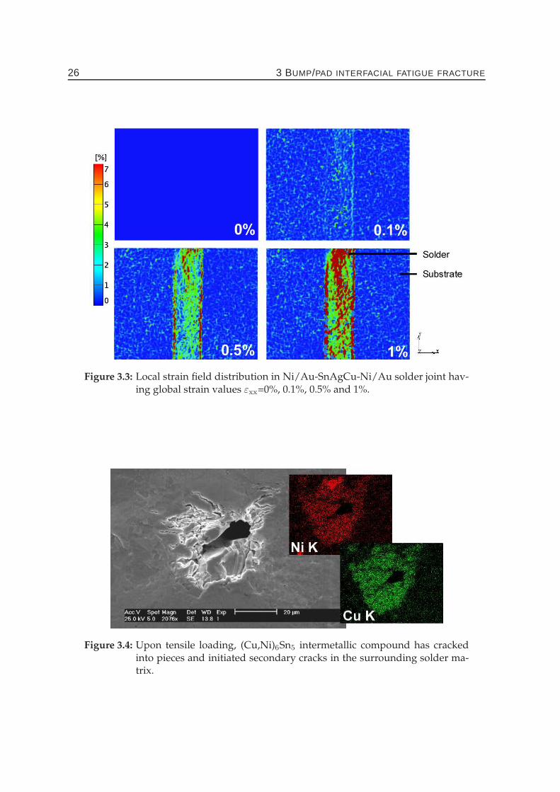
Figure 3.3 shows the local strain field distribution in a soldered joint under tensileloading at various global strain values. SnAgCu solder is situated in the middle andon the left and right is the Ni/Au substrate. Strain fields are monitored throughoutthe deforming region until 1% strain level is reached. Strain is distributed homoge-neously at the start of experiment, up to a threshold value of ∼0.04%. After 0.04%global strain, local strain fields at the bonding interfaces are observed to be higherthan the strain in the bulk solder, indicating damage localization. With further in-crease in global strain, a fairly homogeneous strain distribution is seen in the solder.At 0.5% global strain, local strain in the solder corresponds to 4%, which is well in theplastic region. At later stages, crack propagation is observed at the interfacial regionshaving the highest local strain values. Post-mortem analysis showed that regionsnear the solder interface were heavily deformed. Figure 3.4 shows an (Cu,Ni)6Sn5
intermetallic compound that has delaminated from the solder matrix and cracked,thereby triggered secondary cracks to initiate in its surroundings. Intermetallic com-pounds form during reflow and they act as stress concentration points due to theirsharp edges. Furthermore, they are more brittle than the matrix (Hardness HCu6Sn5
=3.7 GPa, HSnAgCu= 0.83 GPa [16]).
26 3 BUMP/PAD INTERFACIAL FATIGUE FRACTURE
Figure 3.3: Local strain field distribution in Ni/Au-SnAgCu-Ni/Au solder joint hav-ing global strain values εxx=0%, 0.1%, 0.5% and 1%.
Figure 3.4: Upon tensile loading, (Cu,Ni)6Sn5 intermetallic compound has crackedinto pieces and initiated secondary cracks in the surrounding solder ma-trix.
3.3 RESULTS OF FATIGUE TESTS 27
0 500 1000 15005
10
15
20
25
N (cycles)
Shear
Str
ess [M
Pa]
Type A
Type B
Type C
500 mm 1e3 mm 10 mm
Figure 3.5: Stress drop regimes observed in cyclic strain controlled experiments andtypical micrographs corresponding to A, B and C failure types.
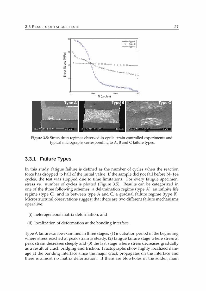
3.3.1 Failure Types
In this study, fatigue failure is defined as the number of cycles when the reactionforce has dropped to half of the initial value. If the sample did not fail before N=1e4cycles, the test was stopped due to time limitations. For every fatigue specimen,stress vs. number of cycles is plotted (Figure 3.5). Results can be categorized inone of the three following schemes: a delamination regime (type A), an infinite liferegime (type C), and in between type A and C, a gradual failure regime (type B).Microstructural observations suggest that there are two different failure mechanismsoperative:
(i) heterogeneous matrix deformation, and
(ii) localization of deformation at the bonding interface.
Type A failure can be examined in three stages: (1) incubation period in the beginningwhere stress reached at peak strain is steady, (2) fatigue failure stage where stress atpeak strain decreases steeply and (3) the last stage where stress decreases graduallyas a result of crack bridging and friction. Fractographs show highly localized dam-age at the bonding interface since the major crack propagates on the interface andthere is almost no matrix deformation. If there are blowholes in the solder, main
28 3 BUMP/PAD INTERFACIAL FATIGUE FRACTURE
crack preferentially propagates on that weaker interface. Here the dominating fail-ure mechanism is delamination. Strain life is between N=1000-2000 cycles. Type Afailure is observed in the fatigue specimens in which the initial stress was highest.In addition, solder volume being less than ∼1 mm3 seemed to increase the tendencytowards delamination.
An infinite fatigue life (type C) is observed when the initial stress was less than 17MPa, and/or when solder volume exceeded 3 mm3. This suggests that strain lifeof SnAgCu solder joints is not only determined by the initial stress state but alsodepends on geometry. In the solder matrix many small cracks are observed. Thepattern of these cracks coincides with the pattern observed in the polarized imagestaken before the fatigue tests. For the present case, it can be concluded that fatiguecracks initiate on domain boundaries where there is a slight difference in the crystal-lographic orientation. Another interesting point was that slip lines appeared in β-Sndendrite arms but not in the eutectic matrix, most probably due to the hard inter-metallic particles in the ternary eutectic matrix. In type C specimens, a major fatiguecrack was still not observed after N=1e4 cycles. These results suggest that a fatiguelimit exists in both normal and tangential directions of the bonding interface, with aroughly estimated value of σf=17 MPa. In order to verify the fatigue limit, a separatetesting procedure is necessary.
Specimens in which fatigue failure proceeds gradually are referred as type B. Frac-tographs show heavy deformation in the matrix as well as an interfacial crack whichhas led to failure. Surface relief in the solder matrix consists of slip in β-Sn dendrites,many short cracks on domain boundaries in the eutectic matrix, deformation bands45◦ in the loading direction, and secondary cracks on grain boundaries. Strain life isbetween N=2000-5000 cycles. Here, both deformation mechanisms mentioned aboveare operative.
Whether the fracture behavior will be abrupt (by delamination) or gradual dependson local soldering conditions. Existence of manufacturing defects on the surface, un-der wetting, insufficient intermetallic growth will favor delamination leading to asudden failure. If the fatigue crack propagation is taking place in the solder veryclose to the bump/pad, dimples and fatigue striations are observed in the frac-tographs and the expected failure type is gradual.
Shear specimens show more matrix deformation than tensile specimens. This sug-gests that the interfacial region is weaker in the normal direction than in the tangen-tial direction. In the tangential direction, the scallop geometry of intermetallic com-pounds serve as a mechanical barrier and solder cannot delaminate easily. Therefore,energy dissipation due to plastic deformation in the matrix is promoted over dam-age localization at the bonding interface. This observation is in accordance with theresults shown in Section 2.3.2.
3.3 RESULTS OF FATIGUE TESTS 29
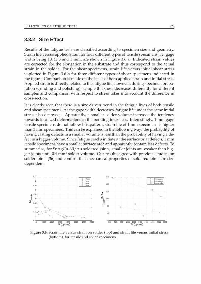
3.3.2 Size Effect
Results of the fatigue tests are classified according to specimen size and geometry.Strain life versus applied strain for four different types of tensile specimens, i.e. gagewidth being 10, 5, 3 and 1 mm, are shown in Figure 3.6 a. Indicated strain valuesare corrected for the elongation in the substrate and thus correspond to the actualstrain in the solder. For the shear specimens, strain life versus initial shear stressis plotted in Figure 3.6 b for three different types of shear specimens indicated inthe figure. Comparison is made on the basis of both applied strain and initial stress.Applied strain is directly related to the fatigue life, however, during specimen prepa-ration (grinding and polishing), sample thickness decreases differently for differentsamples and comparison with respect to stress takes into account the difference incross-section.
It is clearly seen that there is a size driven trend in the fatigue lives of both tensileand shear specimens. As the gage width decreases, fatigue life under the same initialstress also decreases. Apparently, a smaller solder volume increases the tendencytowards localized deformations at the bonding interfaces. Interestingly, 1 mm gagetensile specimens do not follow this pattern; strain life of 1 mm specimens is higherthan 3 mm specimens. This can be explained in the following way: the probability ofhaving casting defects in a smaller volume is less than the probability of having a de-fect in a bigger volume. Since fatigue cracks initiate at the surface or at defects, 1 mmtensile specimens have a smaller surface area and apparently contain less defects. Tosummarize, for SnAgCu-Ni/Au soldered joints, smaller joints are weaker than big-ger joints until 0.4 mm3 solder volume. Our results agree with previous studies onsolder joints [36] and confirm that mechanical properties of soldered joints are sizedependent.
0 1000 2000 3000 4000 5000 6000 70000.5
1
1.5
2
2.5
3
3.5
4
4.5
5
5.5
N (cycles)
∆εte
nsile
10mm5mm3mm1mm
400 600 800 1000 1200 1400 1600 1800 2000 220040
60
80
100
120
140
160
N (cycles)
σ shea
r [MP
a]
3mm double1mm double3mm single
Figure 3.6: Strain life versus strain on solder (top) and strain life versus initial stress(bottom), for tensile and shear specimens.
30 3 BUMP/PAD INTERFACIAL FATIGUE FRACTURE
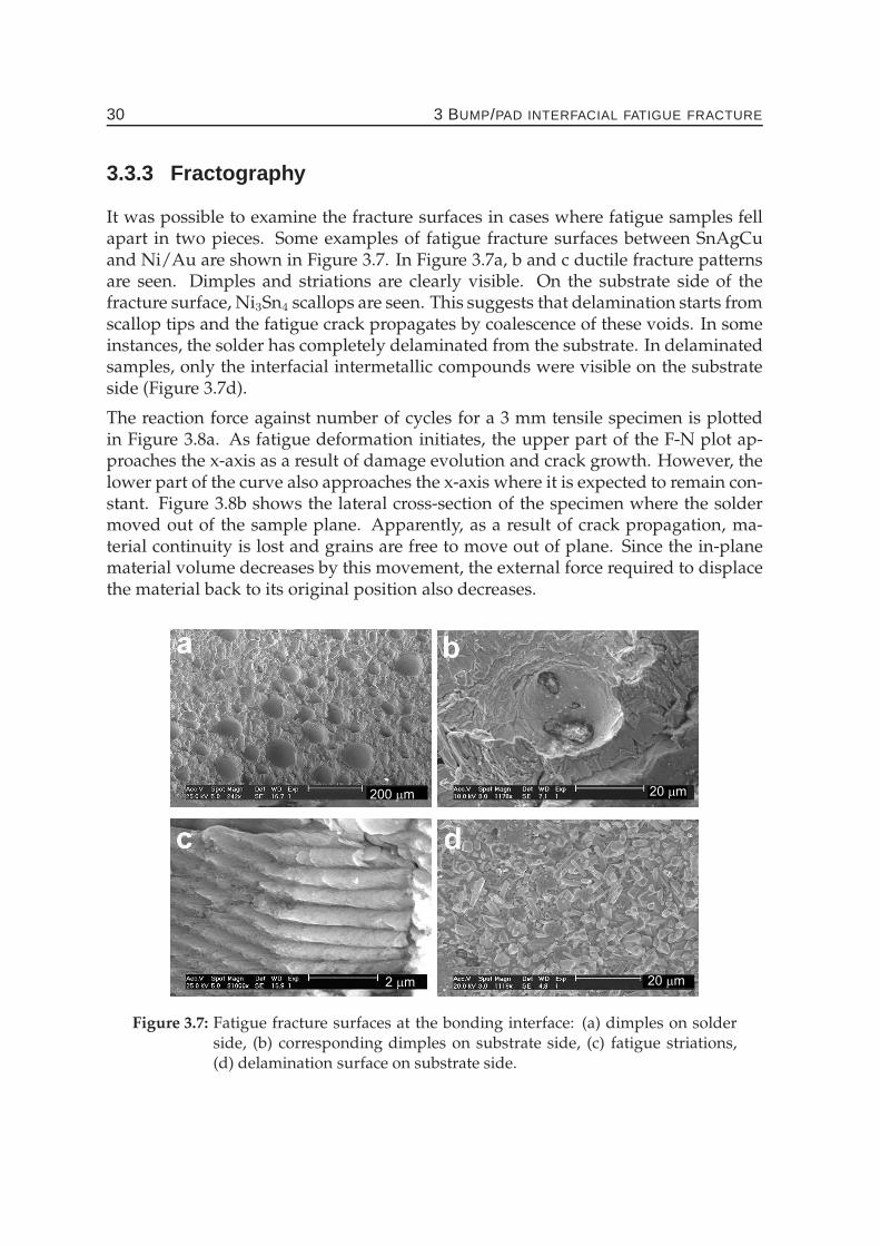
3.3.3 Fractography
It was possible to examine the fracture surfaces in cases where fatigue samples fellapart in two pieces. Some examples of fatigue fracture surfaces between SnAgCuand Ni/Au are shown in Figure 3.7. In Figure 3.7a, b and c ductile fracture patternsare seen. Dimples and striations are clearly visible. On the substrate side of thefracture surface, Ni3Sn4 scallops are seen. This suggests that delamination starts fromscallop tips and the fatigue crack propagates by coalescence of these voids. In someinstances, the solder has completely delaminated from the substrate. In delaminatedsamples, only the interfacial intermetallic compounds were visible on the substrateside (Figure 3.7d).
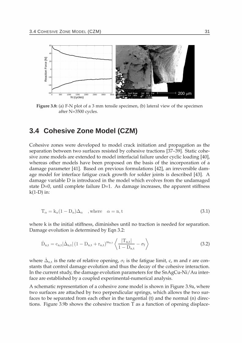
The reaction force against number of cycles for a 3 mm tensile specimen is plottedin Figure 3.8a. As fatigue deformation initiates, the upper part of the F-N plot ap-proaches the x-axis as a result of damage evolution and crack growth. However, thelower part of the curve also approaches the x-axis where it is expected to remain con-stant. Figure 3.8b shows the lateral cross-section of the specimen where the soldermoved out of the sample plane. Apparently, as a result of crack propagation, ma-terial continuity is lost and grains are free to move out of plane. Since the in-planematerial volume decreases by this movement, the external force required to displacethe material back to its original position also decreases.
200 mm 20 mm
2 mm 20 mm
Figure 3.7: Fatigue fracture surfaces at the bonding interface: (a) dimples on solderside, (b) corresponding dimples on substrate side, (c) fatigue striations,(d) delamination surface on substrate side.
3.4 COHESIVE ZONE MODEL (CZM) 31
0 500 1000 1500 2000 2500 3000 3500−60
−40
−20
0
20
40
60
N (cycles)
Rea
ctio
n F
orce
[N]
200 mm
Figure 3.8: (a) F-N plot of a 3 mm tensile specimen, (b) lateral view of the specimenafter N=3500 cycles.
3.4 Cohesive Zone Model (CZM)
Cohesive zones were developed to model crack initiation and propagation as theseparation between two surfaces resisted by cohesive tractions [37–39]. Static cohe-sive zone models are extended to model interfacial failure under cyclic loading [40],whereas other models have been proposed on the basis of the incorporation of adamage parameter [41]. Based on previous formulations [42], an irreversible dam-age model for interface fatigue crack growth for solder joints is described [43]. Adamage variable D is introduced in the model which evolves from the undamagedstate D=0, until complete failure D=1. As damage increases, the apparent stiffnessk(1-D) in:
Tα = kα(1 − Dα)∆α ,where α = n, t (3.1)
where k is the initial stiffness, diminishes until no traction is needed for separation.Damage evolution is determined by Eqn 3.2:
Dn,t = cn,t|∆n,t| (1 − Dn,t + rn,t)mn,t
⟨ |Tn,t|1 − Dn,t
− σf
⟩
(3.2)
where ∆n,t is the rate of relative opening, σf is the fatigue limit, c, m and r are con-stants that control damage evolution and thus the decay of the cohesive interaction.In the current study, the damage evolution parameters for the SnAgCu-Ni/Au inter-face are established by a coupled experimental-numerical analysis.
A schematic representation of a cohesive zone model is shown in Figure 3.9a, wheretwo surfaces are attached by two perpendicular springs, which allows the two sur-faces to be separated from each other in the tangential (t) and the normal (n) direc-tions. Figure 3.9b shows the cohesive traction T as a function of opening displace-
32 3 BUMP/PAD INTERFACIAL FATIGUE FRACTURE
D m[ m] N (cycles)
T[M
Pa]
F [N
]
Figure 3.9: Constitutive behavior of the CZM.
ment ∆ for various number of cycles. A cyclic sinusoidal displacement is appliedto the upper nodes and the lower nodes are restricted. As maximum opening dis-placement increases, maximum traction decreases as a result of damage evolutionvia cyclic loading. The cohesive zone formulation is implemented in the commercialfinite element package MSC.Marc/Mentat as a user defined element in 2D which canbe used both in plane strain and in plane stress to describe the interfacial interaction.
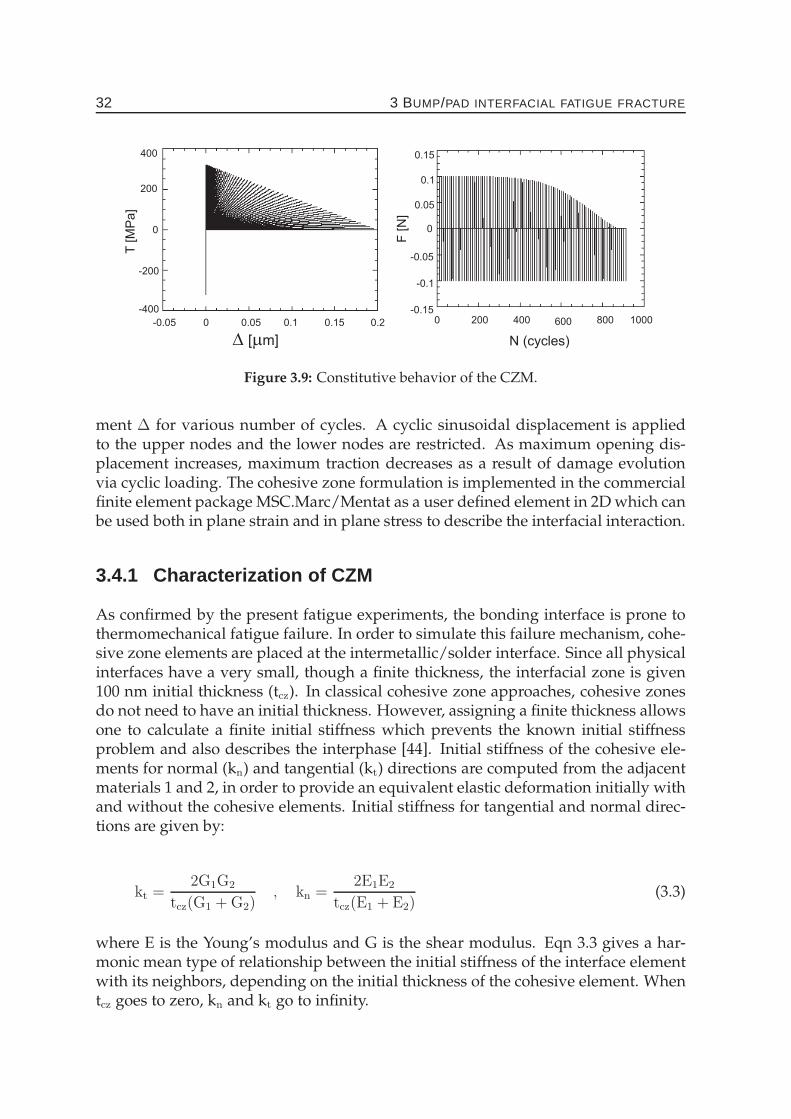
3.4.1 Characterization of CZM
As confirmed by the present fatigue experiments, the bonding interface is prone tothermomechanical fatigue failure. In order to simulate this failure mechanism, cohe-sive zone elements are placed at the intermetallic/solder interface. Since all physicalinterfaces have a very small, though a finite thickness, the interfacial zone is given100 nm initial thickness (tcz). In classical cohesive zone approaches, cohesive zonesdo not need to have an initial thickness. However, assigning a finite thickness allowsone to calculate a finite initial stiffness which prevents the known initial stiffnessproblem and also describes the interphase [44]. Initial stiffness of the cohesive ele-ments for normal (kn) and tangential (kt) directions are computed from the adjacentmaterials 1 and 2, in order to provide an equivalent elastic deformation initially withand without the cohesive elements. Initial stiffness for tangential and normal direc-tions are given by:
kt =2G1G2
tcz(G1 + G2), kn =
2E1E2
tcz(E1 + E2)(3.3)
where E is the Young’s modulus and G is the shear modulus. Eqn 3.3 gives a har-monic mean type of relationship between the initial stiffness of the interface elementwith its neighbors, depending on the initial thickness of the cohesive element. Whentcz goes to zero, kn and kt go to infinity.
3.4 COHESIVE ZONE MODEL (CZM) 33
800 1000 1200 1400 1600 1800−1
−0.8
−0.6
−0.4
−0.2
0
0.2
0.4
0.6
0.8
1
N (cycles)
σ norm
aliz
ed
e=1 f=1e6e=1 f=1e3e=2 f=1e3e=3 f=1e3e=4 f=1e3
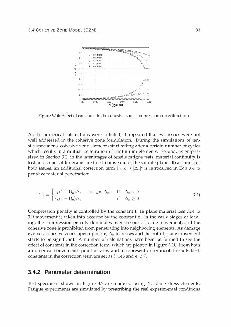
Figure 3.10: Effect of constants in the cohesive zone compression correction term.
As the numerical calculations were initiated, it appeared that two issues were notwell addressed in the cohesive zone formulation. During the simulations of ten-sile specimens, cohesive zone elements start failing after a certain number of cycleswhich results in a mutual penetration of continuum elements. Second, as empha-sized in Section 3.3, in the later stages of tensile fatigue tests, material continuity islost and some solder grains are free to move out of the sample plane. To account forboth issues, an additional correction term f ∗ kn ∗ |∆n|e is introduced in Eqn 3.4 topenalize material penetration:
Tn =
{
kn(1 − Dn)∆n − f ∗ kn ∗ |∆n|e if ∆n < 0
kn(1 − Dn)∆n if ∆n ≥ 0(3.4)
Compression penalty is controlled by the constant f. In plane material loss due to3D movement is taken into account by the constant e. In the early stages of load-ing, the compression penalty dominates over the out of plane movement, and thecohesive zone is prohibited from penetrating into neighboring elements. As damageevolves, cohesive zones open up more, ∆n increases and the out-of-plane movementstarts to be significant. A number of calculations have been performed to see theeffect of constants in the correction term, which are plotted in Figure 3.10. From botha numerical convenience point of view and to represent experimental results best,constants in the correction term are set as f=1e3 and e=3.7.
3.4.2 Parameter determination
Test specimens shown in Figure 3.2 are modeled using 2D plane stress elements.Fatigue experiments are simulated by prescribing the real experimental conditions
34 3 BUMP/PAD INTERFACIAL FATIGUE FRACTURE
Table 3.1: Cohesive zone parameters for normal and tangential direction characteriz-ing interfacial separation in a SnAgCu solder joint under cyclic loading.
Tensile experiments Gage [mm] ǫpeak % cn [N/mm] mn rExp. 11 5 2.0 68000 3.16 1e-6Exp. 12 1 1.7 68000 3.16 3e-5Exp. 13 3 1.4 68000 3.16 1e-6Shear experiments Gage [mm] γpeak % ct [N/mm] mt rExp. 21 3 1.8 46000 3.14 4e-5Exp. 22 3 2.9 48000 3.13 3e-6
at the specimen boundaries. Cohesive zone elements are placed between the in-termetallic compound and solder, where fatigue failure is typically observed. Inthe simulations, damage evolution parameters are tuned to obtain the same globalstress-strain response as measured in the experiments. By modeling the completetest-specimen, experimental stress-strain data is converted indirectly to the traction-displacement in the cohesive zones. A set of damage evolution parameters c, m andr in Eqn 3.2 is obtained which characterizes the strength of SnAgCu-Ni/Au bondinginterface under cyclic strain. Among these, c is related to the damage initiation be-fore any softening starts. The power parameter m takes values between 3 and 3.3,and is responsible from the sharpness of the softening. Parameter r takes values closeto 0+, and is the slope of the softening tail in the last stages of deformation. Smallervalues of r predict a longer life time.
In the present model, damage evolution is activated only during loading, and inhib-ited during unloading in the cyclic load sequence. SnAgCu is modeled as indicatedin Section 3.2, with Poisson’s ratio ν=0.35. Young’s modulus and Poisson’s ratio ofNi is taken as 198 GPa and 0.31. Young’s modulus of the intermetallic compoundNi3Sn4 is reported as 140.4 GPa [45], and Poisson’s ratio is taken as ν=0.2. Substratenickel and the intermetallic compound Ni3Sn4 are modeled linear elastically, sincethe stress state at the peak of the cycle is safely below the yield stress of both materi-als. Fatigue experiments were conducted at room temperature. SnAgCu is modeledby a time independent elasto-plastic material model combined with a steady-statecreep model for bulk SnAgCu [30] shown in Eqn 3.5, where A1 and A2 are 4e-7 and1e-12 s−1, Q1 and Q2 are 26.8 and 61.4 kJ/mol, n1 and n2 are 3 and 12, respectively.
ε = A1
(
σ
σN
)n1
exp
(
−Q1
RT
)
+ A2
(
σ
σN
)n2
exp
(
−Q2
RT
)
(3.5)
Blowholes are a common problem in soldering. A blowhole is a void at thebump/pad junction which decreases the cross-sectional area and therefore decreasesthe strength of the interface. For this reason, test specimens were examined in thepresence of blowholes. In the numerical simulation of these specimens, initial dam-age in the corresponding cohesive zone elements is set to 1. Figure 3.11 shows the
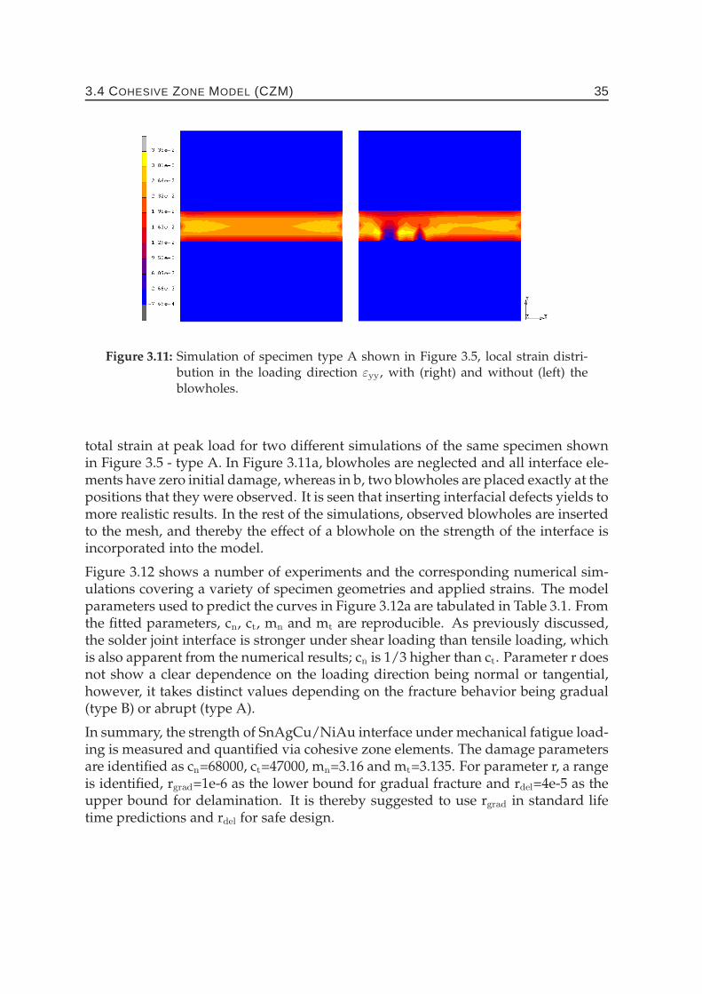
3.4 COHESIVE ZONE MODEL (CZM) 35
Figure 3.11: Simulation of specimen type A shown in Figure 3.5, local strain distri-bution in the loading direction εyy, with (right) and without (left) theblowholes.
total strain at peak load for two different simulations of the same specimen shownin Figure 3.5 - type A. In Figure 3.11a, blowholes are neglected and all interface ele-ments have zero initial damage, whereas in b, two blowholes are placed exactly at thepositions that they were observed. It is seen that inserting interfacial defects yields tomore realistic results. In the rest of the simulations, observed blowholes are insertedto the mesh, and thereby the effect of a blowhole on the strength of the interface isincorporated into the model.
Figure 3.12 shows a number of experiments and the corresponding numerical sim-ulations covering a variety of specimen geometries and applied strains. The modelparameters used to predict the curves in Figure 3.12a are tabulated in Table 3.1. Fromthe fitted parameters, cn, ct, mn and mt are reproducible. As previously discussed,the solder joint interface is stronger under shear loading than tensile loading, whichis also apparent from the numerical results; cn is 1/3 higher than ct. Parameter r doesnot show a clear dependence on the loading direction being normal or tangential,however, it takes distinct values depending on the fracture behavior being gradual(type B) or abrupt (type A).
In summary, the strength of SnAgCu/NiAu interface under mechanical fatigue load-ing is measured and quantified via cohesive zone elements. The damage parametersare identified as cn=68000, ct=47000, mn=3.16 and mt=3.135. For parameter r, a rangeis identified, rgrad=1e-6 as the lower bound for gradual fracture and rdel=4e-5 as theupper bound for delamination. It is thereby suggested to use rgrad in standard lifetime predictions and rdel for safe design.

36 3 BUMP/PAD INTERFACIAL FATIGUE FRACTURE
0 500 1000 1500 2000 2500−80
−60
−40
−20
0
20
40
60
80
N (cycles)
σ [M
Pa]
exp.11sim.11exp.12sim.12exp.13sim.13exp.21sim.21exp.22sim.22
Figure 3.12: Comparison of experimental results and numerical calculations.
3.5 Application to SnAgCu solder interconnect
The cohesive zone parameters given above are used to simulate a solder bump hav-ing the dimensions 760 µm diameter, 500 µm height and 100 µm thickness in 2Dplane stress. The solder material is SnAgCu, metallization is 20 µm copper pad and10 µm nickel diffusion barrier. Between the metallization and solder, there is a 2 µmthick Ni3Sn4 intermetallic layer. Cohesive zone (cz) elements having a 100 nm initialthickness are placed between the solder and the intermetallic layer. Bottom nodes areconstrained in both x and y directions, and the middle top node is loaded in cyclicshear. All material properties are the same as in the previous section. Copper ismodeled linear elastically with the material parameters E=128 GPa and ν=0.35. Thegeometry of the solder bump and the prescribed loading is shown in Figure 3.13.Numerical analysis is carried out at 1% alternating cyclic strain for 5000 cycles. Ateach cohesive zone an effective damage value Deff is calculated from the normal andtangential damage components according to the following relation:
Deff = (D2t + D2
n − DtDn)1
2 (3.6)
Contour plot of effective damage Deff at the end of cycles N=0, 1000, 3000 and 5000 isshown in Figure 3.14. For visibility nodal values are linearly averaged in the contourplot. Thus, damage is made visible through the neighboring continuum elements,only for visualization purposes.
The solder ball geometry does not allow to simply justify a plane deformation state.The solder ball model is run with a plane stress and a plane strain assumption. Dam-age values for the plane stress case is higher than the plane strain case with the same

3.5 APPLICATION TO SNAGCU SOLDER INTERCONNECT 37
0 10 20 30 40 50 60−1
−0.8
−0.6
−0.4
−0.2
0
0.2
0.4
0.6
0.8
1
t [sec]
Nor
mal
ized
str
ain
1 cycle
Figure 3.13: (a) 2D SnAgCu solder ball with Cu/Ni/Au metallization, (b) Prescribedloading on the top middle node εxx.
boundary and loading conditions. Thus plane stress assumption provides a lowerbound for the fatigue life in the present study, which is preferential from an engi-neering perspective.
To summarize the discussion so far, an adequate agreement between experimentaland numerical work has been established, whereby the cohesive zone approach isproven to be an effective tool in solder joint fatigue failure simulation. The model isnumerically stable, and has the potential to be extended to chip size modeling andcomponent life time predictions. The proposed model has the potential for blowholesto be included in the calculation, provided that adequate data on blowhole size anddistribution specific to the manufacturing procedure is known in advance.
Figure 3.14: Effective damage (Deff ) in a SnAgCu solder bump after indicated numberof cycles of shear strain.
38 3 BUMP/PAD INTERFACIAL FATIGUE FRACTURE
3.6 Conclusions
A combined experimental-numerical study on solder joint fatigue failure is carriedout. Ni/Au-SnAgCu solder joints are tested under cyclic shear and cyclic tensionfor different specimen geometries and strain amplitudes. From the qualitative andquantitative data obtained, interfacial separation due to fatigue damage evolution atthe bump/pad interface is simulated using cohesive zone elements. The followingconclusions are drawn from the present study:
• From the local strain fields observed in a soldered joint under tensile loading,strain localization is seen to be strongly microstructure dependent. Highestlocal strains are observed at the solder joint interface followed by grain bound-aries.
• Two different microstructural failure mechanisms are observed; i.e. heteroge-neous matrix deformation and localization of deformation at the bonding in-terface. The interfacial failure mode is typically favored at a high initial stress,and small solder volume.
• Strain life of soldered joints is size dependent.
• A strain life fatigue limit for the SnAgCu-Ni/Au bonding interface is observed.
• Cohesive zone material parameters for bump/pad fatigue crack propagationhave been established for normal and tangential directions separately usingdifferent sample geometries and strain amplitudes.
• An adequate agreement between experimental and numerical work has beenestablished, whereby the cohesive zone approach is proven to be an effectivetool in solder joint fatigue failure simulation. The model is numerically stable,and has the potential to be extended to chip size modeling and component lifetime predictions.
At present, a mechanical model for cyclic mechanical loading has been established.This study is complemented in Chapter 4 by thermally cycled non-constrained sol-der specimens, in order to quantify the bulk damage in the solder due to thermalcycling. Both mechanical and thermal damage mechanisms is combined in Chap-ter 5 to predict thermomechanical damage in solder balls in a BGA assembly.
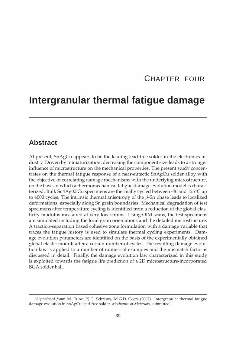
CHAPTER FOUR
Intergranular thermal fatigue damage 1
Abstract
At present, SnAgCu appears to be the leading lead-free solder in the electronics in-dustry. Driven by miniaturization, decreasing the component size leads to a strongerinfluence of microstructure on the mechanical properties. The present study concen-trates on the thermal fatigue response of a near-eutectic SnAgCu solder alloy withthe objective of correlating damage mechanisms with the underlying microstructure,on the basis of which a thermomechanical fatigue damage evolution model is charac-terized. Bulk Sn4Ag0.5Cu specimens are thermally cycled between -40 and 125◦C upto 4000 cycles. The intrinsic thermal anisotropy of the β-Sn phase leads to localizeddeformations, especially along Sn grain boundaries. Mechanical degradation of testspecimens after temperature cycling is identified from a reduction of the global elas-ticity modulus measured at very low strains. Using OIM scans, the test specimensare simulated including the local grain orientations and the detailed microstructure.A traction-separation based cohesive zone formulation with a damage variable thattraces the fatigue history is used to simulate thermal cycling experiments. Dam-age evolution parameters are identified on the basis of the experimentally obtainedglobal elastic moduli after a certain number of cycles. The resulting damage evolu-tion law is applied to a number of numerical examples and the mismatch factor isdiscussed in detail. Finally, the damage evolution law characterized in this studyis exploited towards the fatigue life prediction of a 2D microstructure-incorporatedBGA solder ball.
1Reproduced from: M. Erinc, P.J.G. Schreurs, M.G.D. Geers (2007). Intergranular thermal fatiguedamage evolution in SnAgCu lead-free solder. Mechanics of Materials, submitted.
39

40 4 INTERGRANULAR THERMAL FATIGUE DAMAGE
4.1 Introduction
In microelectronic packages, solder joints are responsible for both the electrical andthe mechanical connection between the printed circuit board (PCB) and the chip.During service, local operating temperatures increase and decrease repeatedly. Com-ponents of the package are exposed to thermomechanical strains arising from differ-ent coefficients of thermal expansion of the materials involved. Cyclic mechanicalstrains in the solder lead to thermomechanical fatigue crack initiation and propa-gation. As a result of legislation and technological requirements, microelectronicsindustry recently switched to eutectic SnAgCu solders as a replacement for the tra-ditional SnPb solder. A broad review on solder materials, reliability issues and sol-der/substrate interactions can be found in the literature [3, 12, 46]. The reliability,failure and lifetime behavior of this solder alloy remains a subject of broad interest,since critical technology sectors (automotive, aerospace, etc.) are still exempted fromusing lead-free solders.
Figure 4.1: A 760 µm diameter SnAgCu BGA solder ball, polarized light image.
Thermomechanical fatigue failure in ball grid array (BGA) packages generally occursat the bump/pad interface. In Chapter 3, a cohesive zone based interfacial separationmodel for the SnAgCu/Ni-Au (bump/pad) interface was developed. Apart from thebump/pad fatigue crack propagation in solder balls, Sn based solders are prone tothermal fatigue damage due to the intrinsic thermal anisotropy of the β-Sn phase. Ithas been well reported in the literature that thermal fatigue in Sn causes intergran-ular fatigue damage [47–51]. This issue is intrinsic to Sn-based solder balls due totheir polycrystalline structure (Figure 4.1). Also, for packages where higher quan-tities of solder are used (i.e. QFN type packages), thermally induced intergranularfatigue failure becomes dominant over solder/pad interfacial fatigue failure [52]. Inthis context, a study on thermomechanical loading in Sn-Ag based lead-free solderswith local grain orientations is given in [53]. Solders are exposed to high homolo-gous temperatures in service use, and therefore their microstructural and mechan-
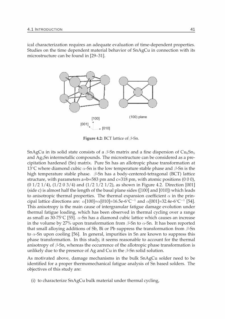
4.1 INTRODUCTION 41
ical characterization requires an adequate evaluation of time-dependent properties.Studies on the time dependent material behavior of SnAgCu in connection with itsmicrostructure can be found in [29–31].
[100]
[010][001]
(100) plane
Figure 4.2: BCT lattice of β-Sn.
SnAgCu in its solid state consists of a β-Sn matrix and a fine dispersion of Cu6Sn5
and Ag3Sn intermetallic compounds. The microstructure can be considered as a pre-cipitation hardened (Sn) matrix. Pure Sn has an allotropic phase transformation at13◦C where diamond cubic α-Sn is the low temperature stable phase and β-Sn is thehigh temperature stable phase. β-Sn has a body-centered-tetragonal (BCT) latticestructure, with parameters a=b=583 pm and c=318 pm, with atomic positions (0 0 0),(0 1/2 1/4), (1/2 0 3/4) and (1/2 1/2 1/2), as shown in Figure 4.2. Direction [001](side c) is almost half the length of the basal plane sides ([100] and [010]) which leadsto anisotropic thermal properties. The thermal expansion coefficient α in the prin-cipal lattice directions are: α[100]=α[010]=16.5e-6◦C−1 and α[001]=32.4e-6◦C−1 [54].This anisotropy is the main cause of intergranular fatigue damage evolution underthermal fatigue loading, which has been observed in thermal cycling over a rangeas small as 30-75◦C [55]. α-Sn has a diamond cubic lattice which causes an increasein the volume by 27% upon transformation from β-Sn to α-Sn. It has been reportedthat small alloying additions of Sb, Bi or Pb suppress the transformation from β-Snto α-Sn upon cooling [56]. In general, impurities in Sn are known to suppress thisphase transformation. In this study, it seems reasonable to account for the thermalanisotropy of β-Sn, whereas the occurrence of the allotropic phase transformation isunlikely due to the presence of Ag and Cu in the β-Sn solid solution.
As motivated above, damage mechanisms in the bulk SnAgCu solder need to beidentified for a proper thermomechanical fatigue analysis of Sn based solders. Theobjectives of this study are:
(i) to characterize SnAgCu bulk material under thermal cycling,
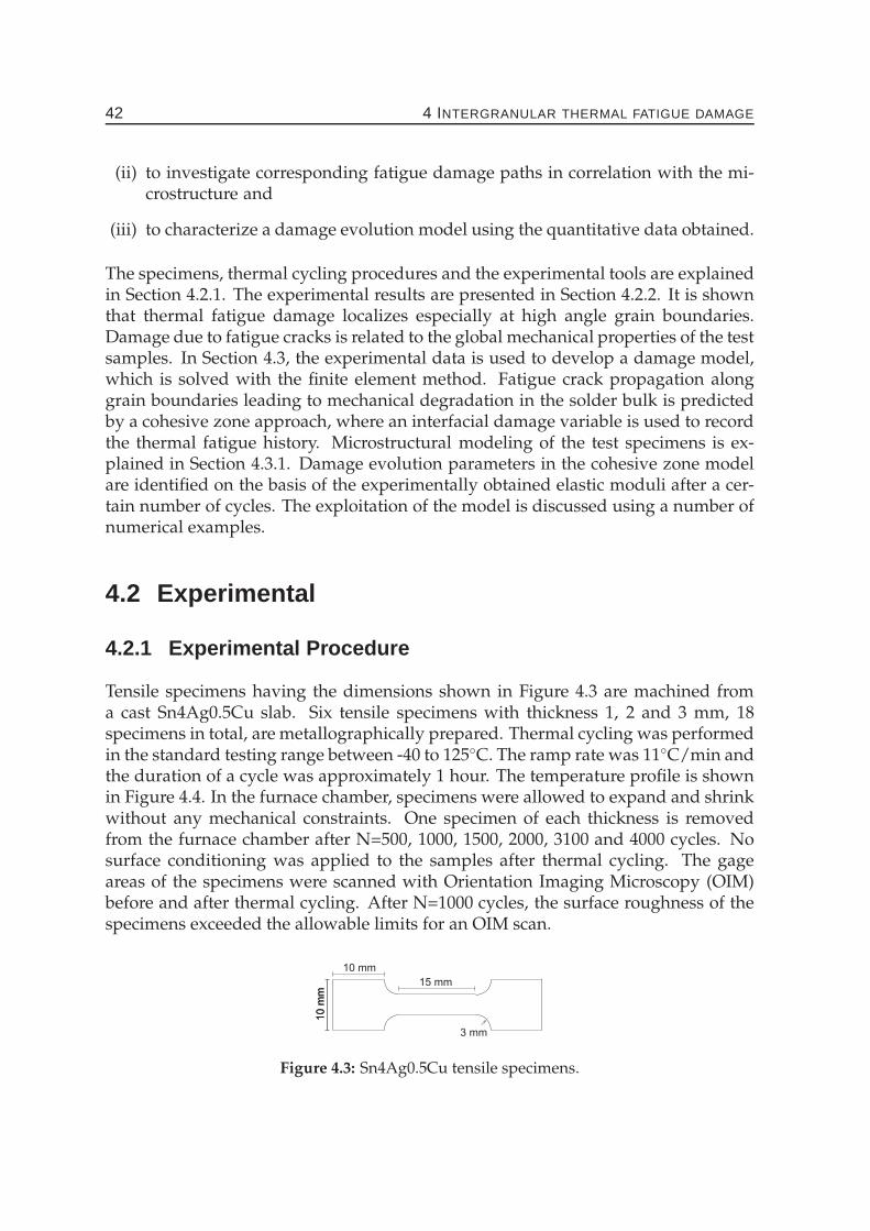
42 4 INTERGRANULAR THERMAL FATIGUE DAMAGE
(ii) to investigate corresponding fatigue damage paths in correlation with the mi-crostructure and
(iii) to characterize a damage evolution model using the quantitative data obtained.
The specimens, thermal cycling procedures and the experimental tools are explainedin Section 4.2.1. The experimental results are presented in Section 4.2.2. It is shownthat thermal fatigue damage localizes especially at high angle grain boundaries.Damage due to fatigue cracks is related to the global mechanical properties of the testsamples. In Section 4.3, the experimental data is used to develop a damage model,which is solved with the finite element method. Fatigue crack propagation alonggrain boundaries leading to mechanical degradation in the solder bulk is predictedby a cohesive zone approach, where an interfacial damage variable is used to recordthe thermal fatigue history. Microstructural modeling of the test specimens is ex-plained in Section 4.3.1. Damage evolution parameters in the cohesive zone modelare identified on the basis of the experimentally obtained elastic moduli after a cer-tain number of cycles. The exploitation of the model is discussed using a number ofnumerical examples.
4.2 Experimental
4.2.1 Experimental Procedure
Tensile specimens having the dimensions shown in Figure 4.3 are machined froma cast Sn4Ag0.5Cu slab. Six tensile specimens with thickness 1, 2 and 3 mm, 18specimens in total, are metallographically prepared. Thermal cycling was performedin the standard testing range between -40 to 125◦C. The ramp rate was 11◦C/min andthe duration of a cycle was approximately 1 hour. The temperature profile is shownin Figure 4.4. In the furnace chamber, specimens were allowed to expand and shrinkwithout any mechanical constraints. One specimen of each thickness is removedfrom the furnace chamber after N=500, 1000, 1500, 2000, 3100 and 4000 cycles. Nosurface conditioning was applied to the samples after thermal cycling. The gageareas of the specimens were scanned with Orientation Imaging Microscopy (OIM)before and after thermal cycling. After N=1000 cycles, the surface roughness of thespecimens exceeded the allowable limits for an OIM scan.
10
mm
10 mm
10
mm
15 mm
3 mm
Figure 4.3: Sn4Ag0.5Cu tensile specimens.

4.2 EXPERIMENTAL 43
t [min]
T[º
C]
a
bc
Figure 4.4: Thermal cycling temperature profile, ramp rate: 11◦C. (a: required profile,b: air in test chamber, c: temperature on sample, Philips Applied Tech-nologies).
After thermal cycling, strain gages were attached to the specimens to measure theoverall Young’s modulus which is used later as a macroscopic damage indicator.Four strain gages were glued on the damaged samples; two perpendicular to theloading direction for temperature compensation and two active gages for the dis-placement measurement. Tensile tests were performed in a computer controlled dou-ble spindle micro-tensile stage shown in Figure 4.5. A 20 N load cell was used andthe clamp speed was equal to 0.5 µm/s. An appropriate strain (in the order of e-5)was applied to produce a stress of ∼2 MPa in the cross-section of the specimen. Thecritical resolved shear stress for some slip systems in Sn is as low as 3-4 MPa [57].Therefore, in order to limit the amount of plasticity in the material, the stress levelwas chosen to be below 2 MPa. The calculations were computed over the elasticrange of the hysteresis curves. A reference elastic modulus value of 64±1 GPa wasmeasured prior to thermal cycling.
Figure 4.5: Double spindle micro-tensile stage (Kammrath&Weiss).
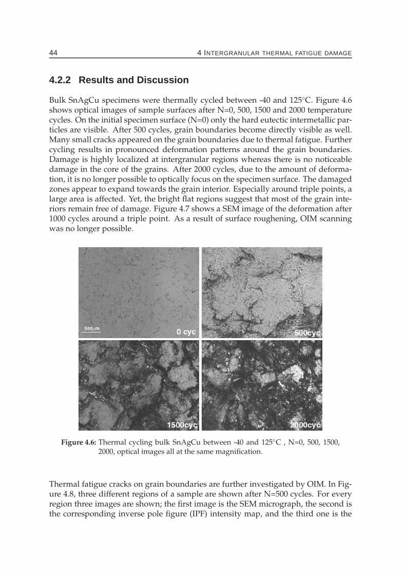
44 4 INTERGRANULAR THERMAL FATIGUE DAMAGE
4.2.2 Results and Discussion
Bulk SnAgCu specimens were thermally cycled between -40 and 125◦C. Figure 4.6shows optical images of sample surfaces after N=0, 500, 1500 and 2000 temperaturecycles. On the initial specimen surface (N=0) only the hard eutectic intermetallic par-ticles are visible. After 500 cycles, grain boundaries become directly visible as well.Many small cracks appeared on the grain boundaries due to thermal fatigue. Furthercycling results in pronounced deformation patterns around the grain boundaries.Damage is highly localized at intergranular regions whereas there is no noticeabledamage in the core of the grains. After 2000 cycles, due to the amount of deforma-tion, it is no longer possible to optically focus on the specimen surface. The damagedzones appear to expand towards the grain interior. Especially around triple points, alarge area is affected. Yet, the bright flat regions suggest that most of the grain inte-riors remain free of damage. Figure 4.7 shows a SEM image of the deformation after1000 cycles around a triple point. As a result of surface roughening, OIM scanningwas no longer possible.
Figure 4.6: Thermal cycling bulk SnAgCu between -40 and 125◦C , N=0, 500, 1500,2000, optical images all at the same magnification.
Thermal fatigue cracks on grain boundaries are further investigated by OIM. In Fig-ure 4.8, three different regions of a sample are shown after N=500 cycles. For everyregion three images are shown; the first image is the SEM micrograph, the second isthe corresponding inverse pole figure (IPF) intensity map, and the third one is the
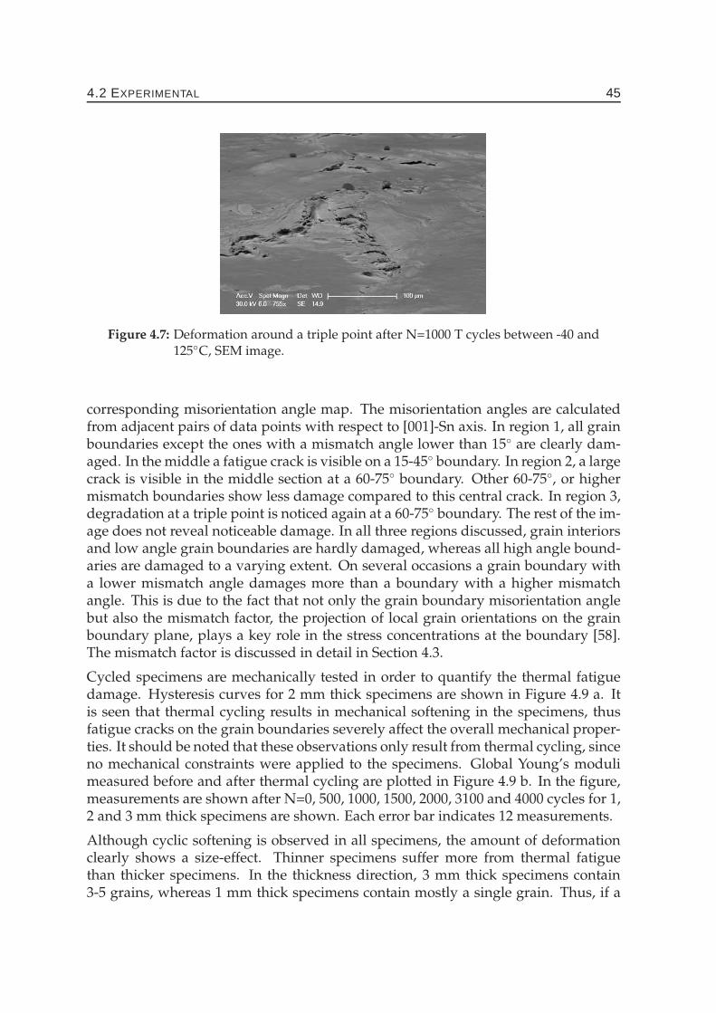
4.2 EXPERIMENTAL 45
Figure 4.7: Deformation around a triple point after N=1000 T cycles between -40 and125◦C, SEM image.
corresponding misorientation angle map. The misorientation angles are calculatedfrom adjacent pairs of data points with respect to [001]-Sn axis. In region 1, all grainboundaries except the ones with a mismatch angle lower than 15◦ are clearly dam-aged. In the middle a fatigue crack is visible on a 15-45◦ boundary. In region 2, a largecrack is visible in the middle section at a 60-75◦ boundary. Other 60-75◦, or highermismatch boundaries show less damage compared to this central crack. In region 3,degradation at a triple point is noticed again at a 60-75◦ boundary. The rest of the im-age does not reveal noticeable damage. In all three regions discussed, grain interiorsand low angle grain boundaries are hardly damaged, whereas all high angle bound-aries are damaged to a varying extent. On several occasions a grain boundary witha lower mismatch angle damages more than a boundary with a higher mismatchangle. This is due to the fact that not only the grain boundary misorientation anglebut also the mismatch factor, the projection of local grain orientations on the grainboundary plane, plays a key role in the stress concentrations at the boundary [58].The mismatch factor is discussed in detail in Section 4.3.
Cycled specimens are mechanically tested in order to quantify the thermal fatiguedamage. Hysteresis curves for 2 mm thick specimens are shown in Figure 4.9 a. Itis seen that thermal cycling results in mechanical softening in the specimens, thusfatigue cracks on the grain boundaries severely affect the overall mechanical proper-ties. It should be noted that these observations only result from thermal cycling, sinceno mechanical constraints were applied to the specimens. Global Young’s modulimeasured before and after thermal cycling are plotted in Figure 4.9 b. In the figure,measurements are shown after N=0, 500, 1000, 1500, 2000, 3100 and 4000 cycles for 1,2 and 3 mm thick specimens are shown. Each error bar indicates 12 measurements.
Although cyclic softening is observed in all specimens, the amount of deformationclearly shows a size-effect. Thinner specimens suffer more from thermal fatiguethan thicker specimens. In the thickness direction, 3 mm thick specimens contain3-5 grains, whereas 1 mm thick specimens contain mostly a single grain. Thus, if a
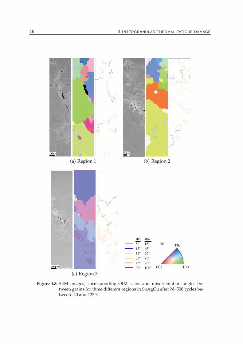
46 4 INTERGRANULAR THERMAL FATIGUE DAMAGE
(a) Region 1 (b) Region 2
(c) Region 3
Tin110
100001
Figure 4.8: SEM images, corresponding OIM scans and misorientation angles be-tween grains for three different regions in SnAgCu after N=500 cycles be-tween -40 and 125◦C.
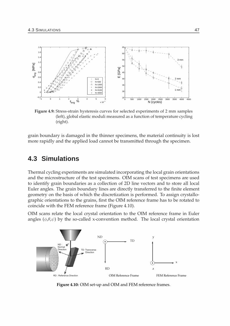
4.3 SIMULATIONS 47
−1 0 1 2 3 4 5 6
x 10−3
−0.2
0
0.2
0.4
0.6
0.8
1
1.2
1.4
1.6
1.8
εeng %
σ eng
[MP
a]
N=0N=500N=1000N=2000N=3100N=4000
0 500 1000 1500 2000 2500 3000 3500 4000 450025
30
35
40
45
50
55
60
65
1 mm
2 mm
3 mm
N (cycles)
E [G
Pa]
Figure 4.9: Stress-strain hysteresis curves for selected experiments of 2 mm samples(left), global elastic moduli measured as a function of temperature cycling(right).
grain boundary is damaged in the thinner specimens, the material continuity is lostmore rapidly and the applied load cannot be transmitted through the specimen.
4.3 Simulations
Thermal cycling experiments are simulated incorporating the local grain orientationsand the microstructure of the test specimens. OIM scans of test specimens are usedto identify grain boundaries as a collection of 2D line vectors and to store all localEuler angles. The grain boundary lines are directly transferred to the finite elementgeometry on the basis of which the discretization is performed. To assign crystallo-graphic orientations to the grains, first the OIM reference frame has to be rotated tocoincide with the FEM reference frame (Figure 4.10).
OIM scans relate the local crystal orientation to the OIM reference frame in Eulerangles (φ,θ,ψ) by the so-called x-convention method. The local crystal orientation
RD : Reference Direction
TD: TransverseDirection
ND :NormalDirection
ND- TD
?
RD
OIM Reference Frame
y
- x
6
z
FEM Reference Frame
Figure 4.10: OIM set-up and OIM and FEM reference frames.
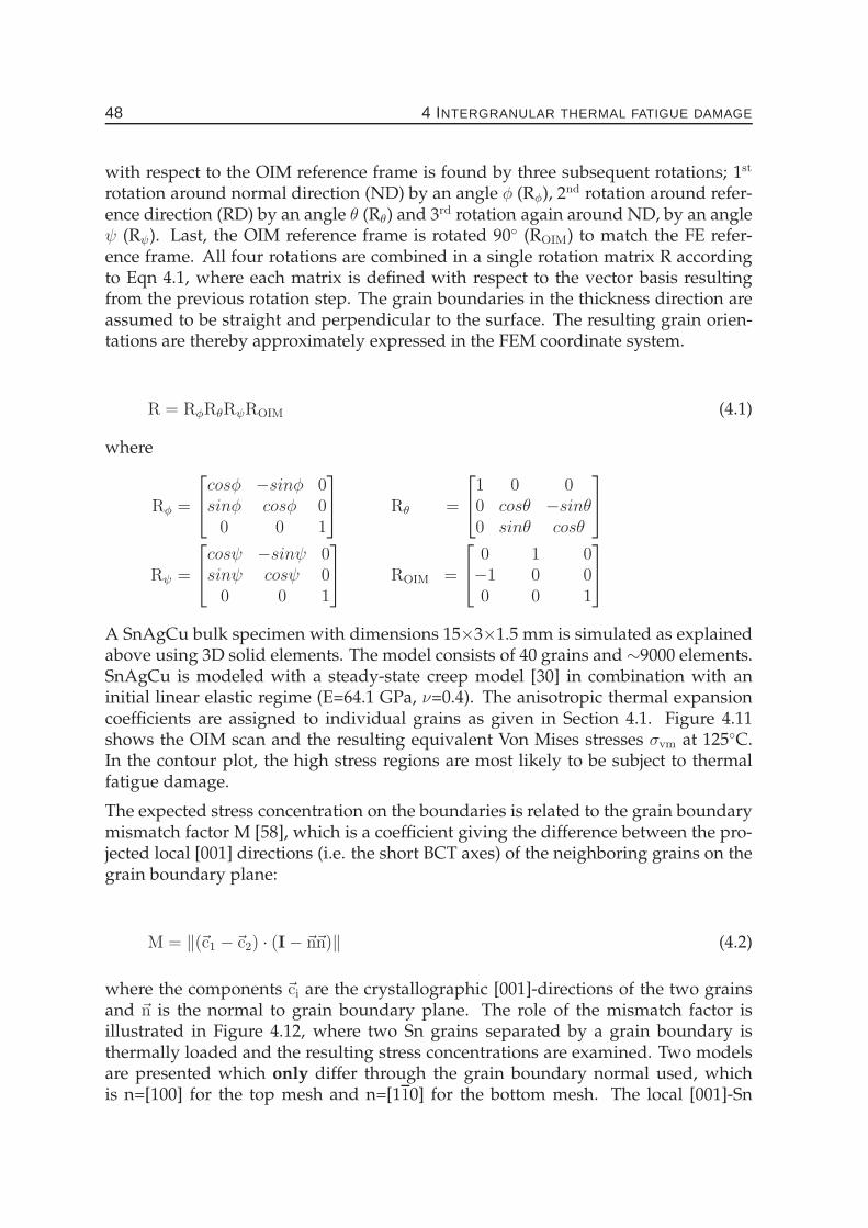
48 4 INTERGRANULAR THERMAL FATIGUE DAMAGE
with respect to the OIM reference frame is found by three subsequent rotations; 1st
rotation around normal direction (ND) by an angle φ (Rφ), 2nd rotation around refer-ence direction (RD) by an angle θ (Rθ) and 3rd rotation again around ND, by an angleψ (Rψ). Last, the OIM reference frame is rotated 90◦ (ROIM) to match the FE refer-ence frame. All four rotations are combined in a single rotation matrix R accordingto Eqn 4.1, where each matrix is defined with respect to the vector basis resultingfrom the previous rotation step. The grain boundaries in the thickness direction areassumed to be straight and perpendicular to the surface. The resulting grain orien-tations are thereby approximately expressed in the FEM coordinate system.
R = RφRθRψROIM (4.1)
where
Rφ =
cosφ −sinφ 0sinφ cosφ 0
0 0 1
Rθ =
1 0 00 cosθ −sinθ0 sinθ cosθ
Rψ =
cosψ −sinψ 0sinψ cosψ 0
0 0 1
ROIM =
0 1 0−1 0 00 0 1
A SnAgCu bulk specimen with dimensions 15×3×1.5 mm is simulated as explainedabove using 3D solid elements. The model consists of 40 grains and ∼9000 elements.SnAgCu is modeled with a steady-state creep model [30] in combination with aninitial linear elastic regime (E=64.1 GPa, ν=0.4). The anisotropic thermal expansioncoefficients are assigned to individual grains as given in Section 4.1. Figure 4.11shows the OIM scan and the resulting equivalent Von Mises stresses σvm at 125◦C.In the contour plot, the high stress regions are most likely to be subject to thermalfatigue damage.
The expected stress concentration on the boundaries is related to the grain boundarymismatch factor M [58], which is a coefficient giving the difference between the pro-jected local [001] directions (i.e. the short BCT axes) of the neighboring grains on thegrain boundary plane:
M = ‖(~c1 −~c2) · (I − ~n~n)‖ (4.2)
where the components ~ci are the crystallographic [001]-directions of the two grainsand ~n is the normal to grain boundary plane. The role of the mismatch factor isillustrated in Figure 4.12, where two Sn grains separated by a grain boundary isthermally loaded and the resulting stress concentrations are examined. Two modelsare presented which only differ through the grain boundary normal used, whichis n=[100] for the top mesh and n=[110] for the bottom mesh. The local [001]-Sn
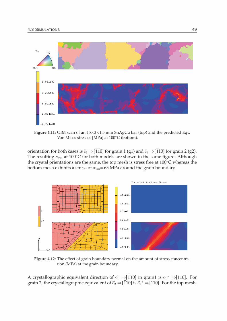
4.3 SIMULATIONS 49
Tin110
100001
Figure 4.11: OIM scan of an 15×3×1.5 mm SnAgCu bar (top) and the predicted Eqv.Von Mises stresses [MPa] at 100◦C (bottom).
orientation for both cases is~c1 ⇒[110] for grain 1 (g1) and~c2 ⇒[110] for grain 2 (g2).The resulting σvm at 100◦C for both models are shown in the same figure. Althoughthe crystal orientations are the same, the top mesh is stress free at 100◦C whereas thebottom mesh exhibits a stress of σvm= 65 MPa around the grain boundary.
Figure 4.12: The effect of grain boundary normal on the amount of stress concentra-tion (MPa) at the grain boundary.
A crystallographic equivalent direction of ~c1 ⇒[110] in grain1 is ~c1∗ ⇒[110]. For
grain 2, the crystallographic equivalent of~c2 ⇒[110] is~c2∗ ⇒[110]. For the top mesh,
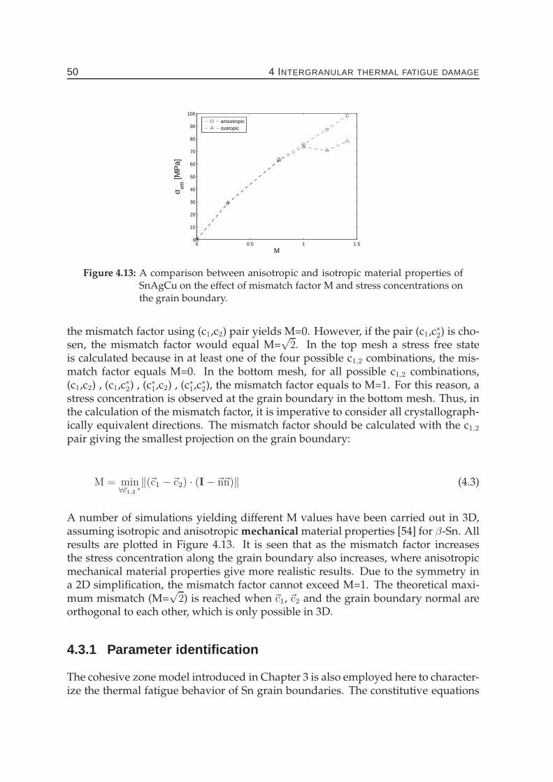
50 4 INTERGRANULAR THERMAL FATIGUE DAMAGE
0 0.5 1 1.50
10
20
30
40
50
60
70
80
90
100
M
σ vm [M
Pa]
anisotropicisotropic
Figure 4.13: A comparison between anisotropic and isotropic material properties ofSnAgCu on the effect of mismatch factor M and stress concentrations onthe grain boundary.
the mismatch factor using (c1,c2) pair yields M=0. However, if the pair (c1,c∗2) is cho-sen, the mismatch factor would equal M=
√2. In the top mesh a stress free state
is calculated because in at least one of the four possible c1,2 combinations, the mis-match factor equals M=0. In the bottom mesh, for all possible c1,2 combinations,(c1,c2) , (c1,c∗2) , (c∗1,c2) , (c∗1,c∗2), the mismatch factor equals to M=1. For this reason, astress concentration is observed at the grain boundary in the bottom mesh. Thus, inthe calculation of the mismatch factor, it is imperative to consider all crystallograph-ically equivalent directions. The mismatch factor should be calculated with the c1,2
pair giving the smallest projection on the grain boundary:
M = min∀~c1,2
∗
‖(~c1 −~c2) · (I − ~n~n)‖ (4.3)
A number of simulations yielding different M values have been carried out in 3D,assuming isotropic and anisotropic mechanical material properties [54] for β-Sn. Allresults are plotted in Figure 4.13. It is seen that as the mismatch factor increasesthe stress concentration along the grain boundary also increases, where anisotropicmechanical material properties give more realistic results. Due to the symmetry ina 2D simplification, the mismatch factor cannot exceed M=1. The theoretical maxi-mum mismatch (M=
√2) is reached when ~c1, ~c2 and the grain boundary normal are
orthogonal to each other, which is only possible in 3D.
4.3.1 Parameter identification
The cohesive zone model introduced in Chapter 3 is also employed here to character-ize the thermal fatigue behavior of Sn grain boundaries. The constitutive equations

4.3 SIMULATIONS 51
Figure 4.14: Sections from a sample mesh with local magnifications showing the gran-ular structure and cohesive zone elements at the grain boundaries.
of the CZM were given in Eqn.s 3.1, 3.2 and 3.6.
The parameter identification is performed on the basis of 1 mm thick test specimens,as justified by the following arguments. First, the 1 mm thick specimens have asingle grain in the thickness and thus grain boundaries perpendicular to the spec-imen surface can be effectively approximated in 2D. For thicker specimens such asimplification cannot be made since there are more grains in the thickness. Second,the biggest solder balls used in BGA packages have a diameter of 760 µm, whichis closely represented by the considered specimens, since their thickness reduces to∼800 µm after the initial surface preparation. The simulations are simplified to 2Das explained above, to prevent laborious 3D calculations. A plane-stress assump-tion is made since out-of plane deformations were observed in the test specimens(Figures 4.6 and 4.7).
The mesh is produced by placing cohesive zone (cz) elements at the grain boundariesusing the OIM output files, such that the tangential direction of the cz element cor-responds with the grain boundary plane, and the normal direction is parallel to thegrain boundary normal. As explained in Section 3.4.1, cz elements are assigned anextremely small, yet finite, initial thickness tcz=100 nm, by which a finite initial stiff-
0 500 1000 1500 2000 2500 3000 3500 4000 450025
30
35
40
45
50
55
60
65
70
N (cycles)
Egl
obal
[GP
a]
exp. resultsc=42000 m=2.95c=42000 m=2.96c=42000 m=2.94c=41000 m=2.94c=41000 m=2.93c=41500 m=2.94
Figure 4.15: Fit of cohesive zone based fatigue damage model to experimental results.
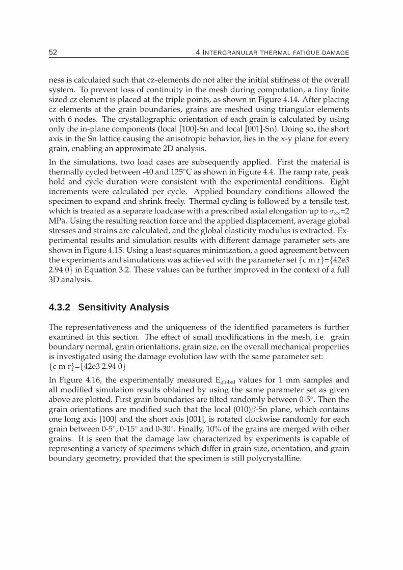
52 4 INTERGRANULAR THERMAL FATIGUE DAMAGE
ness is calculated such that cz-elements do not alter the initial stiffness of the overallsystem. To prevent loss of continuity in the mesh during computation, a tiny finitesized cz element is placed at the triple points, as shown in Figure 4.14. After placingcz elements at the grain boundaries, grains are meshed using triangular elementswith 6 nodes. The crystallographic orientation of each grain is calculated by usingonly the in-plane components (local [100]-Sn and local [001]-Sn). Doing so, the shortaxis in the Sn lattice causing the anisotropic behavior, lies in the x-y plane for everygrain, enabling an approximate 2D analysis.
In the simulations, two load cases are subsequently applied. First the material isthermally cycled between -40 and 125◦C as shown in Figure 4.4. The ramp rate, peakhold and cycle duration were consistent with the experimental conditions. Eightincrements were calculated per cycle. Applied boundary conditions allowed thespecimen to expand and shrink freely. Thermal cycling is followed by a tensile test,which is treated as a separate loadcase with a prescribed axial elongation up to σxx=2MPa. Using the resulting reaction force and the applied displacement, average globalstresses and strains are calculated, and the global elasticity modulus is extracted. Ex-perimental results and simulation results with different damage parameter sets areshown in Figure 4.15. Using a least squares minimization, a good agreement betweenthe experiments and simulations was achieved with the parameter set {c m r}={42e32.94 0} in Equation 3.2. These values can be further improved in the context of a full3D analysis.
4.3.2 Sensitivity Analysis
The representativeness and the uniqueness of the identified parameters is furtherexamined in this section. The effect of small modifications in the mesh, i.e. grainboundary normal, grain orientations, grain size, on the overall mechanical propertiesis investigated using the damage evolution law with the same parameter set:{c m r}={42e3 2.94 0}In Figure 4.16, the experimentally measured Eglobal values for 1 mm samples andall modified simulation results obtained by using the same parameter set as givenabove are plotted. First grain boundaries are tilted randomly between 0-5◦. Then thegrain orientations are modified such that the local (010)β-Sn plane, which containsone long axis [100] and the short axis [001], is rotated clockwise randomly for eachgrain between 0-5◦, 0-15◦ and 0-30◦. Finally, 10% of the grains are merged with othergrains. It is seen that the damage law characterized by experiments is capable ofrepresenting a variety of specimens which differ in grain size, orientation, and grainboundary geometry, provided that the specimen is still polycrystalline.
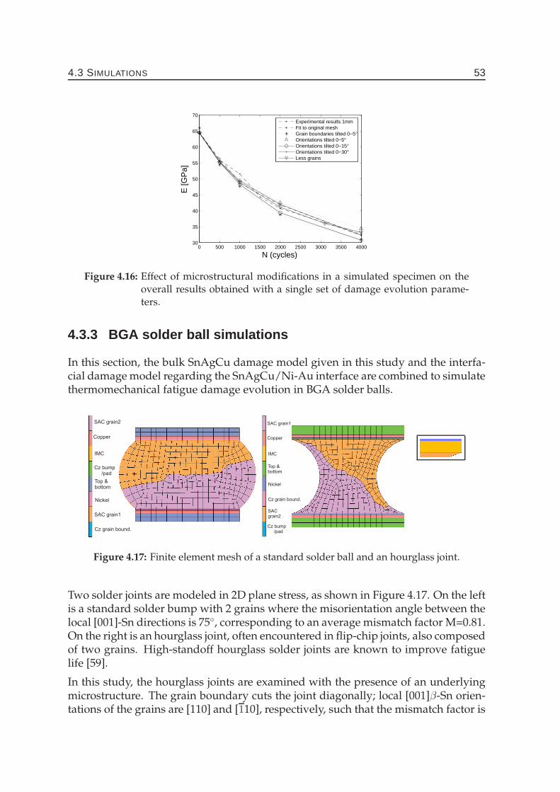
4.3 SIMULATIONS 53
0 500 1000 1500 2000 2500 3000 3500 400030
35
40
45
50
55
60
65
70
N (cycles)
E [G
Pa]
Experimental results 1mmFit to original meshGrain boundaries tilted 0−5°Orientations tilted 0−5°Orientations tilted 0−15°Orientations tilted 0−30°Less grains
Figure 4.16: Effect of microstructural modifications in a simulated specimen on theoverall results obtained with a single set of damage evolution parame-ters.
4.3.3 BGA solder ball simulations
In this section, the bulk SnAgCu damage model given in this study and the interfa-cial damage model regarding the SnAgCu/Ni-Au interface are combined to simulatethermomechanical fatigue damage evolution in BGA solder balls.
SAC grain2
Copper
IMC
Cz bump/pad
Top &bottom
Nickel
SAC grain1
Cz grain bound.
Cz grain bound.
SAC grain1
Copper
IMC
Top &bottom
Nickel
SACgrain2
Cz bump/pad
Figure 4.17: Finite element mesh of a standard solder ball and an hourglass joint.
Two solder joints are modeled in 2D plane stress, as shown in Figure 4.17. On the leftis a standard solder bump with 2 grains where the misorientation angle between thelocal [001]-Sn directions is 75◦, corresponding to an average mismatch factor M=0.81.On the right is an hourglass joint, often encountered in flip-chip joints, also composedof two grains. High-standoff hourglass solder joints are known to improve fatiguelife [59].
In this study, the hourglass joints are examined with the presence of an underlyingmicrostructure. The grain boundary cuts the joint diagonally; local [001]β-Sn orien-tations of the grains are [110] and [110], respectively, such that the mismatch factor is
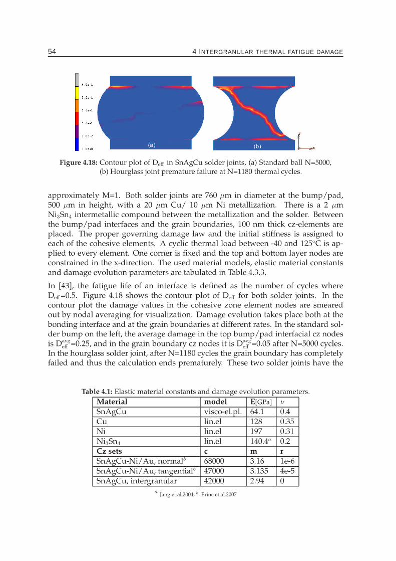
54 4 INTERGRANULAR THERMAL FATIGUE DAMAGE
Figure 4.18: Contour plot of Deff in SnAgCu solder joints, (a) Standard ball N=5000,(b) Hourglass joint premature failure at N=1180 thermal cycles.
approximately M=1. Both solder joints are 760 µm in diameter at the bump/pad,500 µm in height, with a 20 µm Cu/ 10 µm Ni metallization. There is a 2 µmNi3Sn4 intermetallic compound between the metallization and the solder. Betweenthe bump/pad interfaces and the grain boundaries, 100 nm thick cz-elements areplaced. The proper governing damage law and the initial stiffness is assigned toeach of the cohesive elements. A cyclic thermal load between -40 and 125◦C is ap-plied to every element. One corner is fixed and the top and bottom layer nodes areconstrained in the x-direction. The used material models, elastic material constantsand damage evolution parameters are tabulated in Table 4.3.3.
In [43], the fatigue life of an interface is defined as the number of cycles whereDeff=0.5. Figure 4.18 shows the contour plot of Deff for both solder joints. In thecontour plot the damage values in the cohesive zone element nodes are smearedout by nodal averaging for visualization. Damage evolution takes place both at thebonding interface and at the grain boundaries at different rates. In the standard sol-der bump on the left, the average damage in the top bump/pad interfacial cz nodesis Davg
eff =0.25, and in the grain boundary cz nodes it is Davgeff =0.05 after N=5000 cycles.
In the hourglass solder joint, after N=1180 cycles the grain boundary has completelyfailed and thus the calculation ends prematurely. These two solder joints have the
Table 4.1: Elastic material constants and damage evolution parameters.
Material model E[GPa] νSnAgCu visco-el.pl. 64.1 0.4Cu lin.el 128 0.35Ni lin.el 197 0.31Ni3Sn4 lin.el 140.4a 0.2Cz sets c m r
SnAgCu-Ni/Au, normalb 68000 3.16 1e-6SnAgCu-Ni/Au, tangentialb 47000 3.135 4e-5SnAgCu, intergranular 42000 2.94 0
aJang et al.2004, b Erinc et al.2007
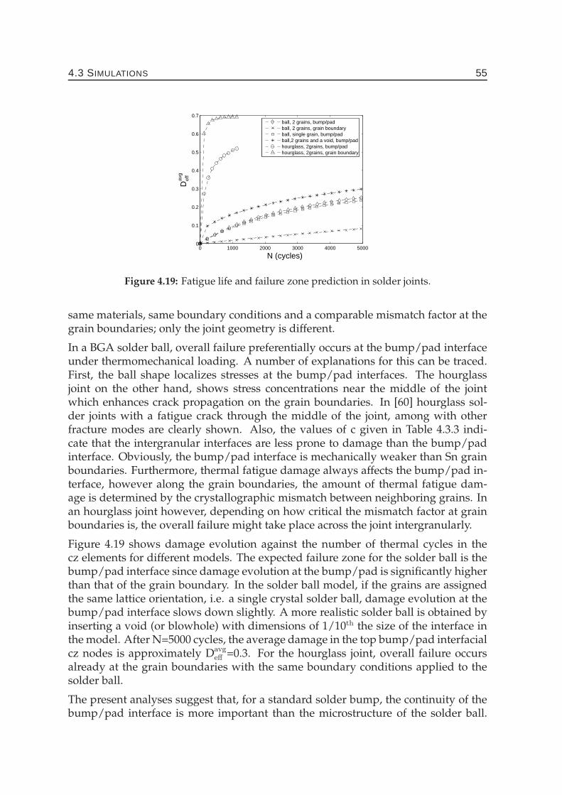
4.3 SIMULATIONS 55
0 1000 2000 3000 4000 50000
0.1
0.2
0.3
0.4
0.5
0.6
0.7
N (cycles)
Def
fav
g
ball, 2 grains, bump/padball, 2 grains, grain boundaryball, single grain, bump/padball,2 grains and a void, bump/padhourglass, 2grains, bump/padhourglass, 2grains, grain boundary
Figure 4.19: Fatigue life and failure zone prediction in solder joints.
same materials, same boundary conditions and a comparable mismatch factor at thegrain boundaries; only the joint geometry is different.
In a BGA solder ball, overall failure preferentially occurs at the bump/pad interfaceunder thermomechanical loading. A number of explanations for this can be traced.First, the ball shape localizes stresses at the bump/pad interfaces. The hourglassjoint on the other hand, shows stress concentrations near the middle of the jointwhich enhances crack propagation on the grain boundaries. In [60] hourglass sol-der joints with a fatigue crack through the middle of the joint, among with otherfracture modes are clearly shown. Also, the values of c given in Table 4.3.3 indi-cate that the intergranular interfaces are less prone to damage than the bump/padinterface. Obviously, the bump/pad interface is mechanically weaker than Sn grainboundaries. Furthermore, thermal fatigue damage always affects the bump/pad in-terface, however along the grain boundaries, the amount of thermal fatigue dam-age is determined by the crystallographic mismatch between neighboring grains. Inan hourglass joint however, depending on how critical the mismatch factor at grainboundaries is, the overall failure might take place across the joint intergranularly.
Figure 4.19 shows damage evolution against the number of thermal cycles in thecz elements for different models. The expected failure zone for the solder ball is thebump/pad interface since damage evolution at the bump/pad is significantly higherthan that of the grain boundary. In the solder ball model, if the grains are assignedthe same lattice orientation, i.e. a single crystal solder ball, damage evolution at thebump/pad interface slows down slightly. A more realistic solder ball is obtained byinserting a void (or blowhole) with dimensions of 1/10th the size of the interface inthe model. After N=5000 cycles, the average damage in the top bump/pad interfacialcz nodes is approximately Davg
eff =0.3. For the hourglass joint, overall failure occursalready at the grain boundaries with the same boundary conditions applied to thesolder ball.
The present analyses suggest that, for a standard solder bump, the continuity of thebump/pad interface is more important than the microstructure of the solder ball.
56 4 INTERGRANULAR THERMAL FATIGUE DAMAGE
However, for an hourglass joint, the microstructure is crucial since existence of criti-cal grain boundaries might cause fatigue crack propagation and overall failure acrossthe joint. Based on the adopted analytical formula for the damage evolution, an es-timate for the lifetime can be computed. The standard solder bump with the goodinterface will fail at their bond/pad interface at N≈27e3 cycles whereas the ball witha blowhole will fail at N≈18e3 thermal cycles between -40 and 125◦C according tothe selected failure criterion. The analysis suggests that a small void such as 1/10length of the interface reduces the fatigue life of the joint by 1/3.
4.4 Conclusions
Thermal fatigue damage mechanisms in bulk Sn4.0Ag0.5Cu lead-free solder are ex-amined in correlation with the underlying microstructure. All observations andresults reflect the response under pure thermal cycling, with no mechanical con-straints. Intergranular fatigue cracks induced by the intrinsic thermal anisotropyof β-Sn are here predicted through the damage in the interfacial cohesive zone ele-ments. The mechanical degradation in the thermally cycled specimens measured bytensile experiments is used to identify the damage evolution parameters using a cou-pled numerical-experimental approach. The representativeness of the parameters isinvestigated by a sensitivity analysis. The model is applied to BGA solder balls, andthe thermomechanical fatigue life is predicted. From the present study, the followingconclusions are drawn:
• Thermal fatigue loading causes local damage patterns along Sn grain bound-aries. At grain boundaries where the local mismatch angle between two grainswas less than 15◦, no significant damage was observed. For higher angleboundaries, the amount of deformation depends on the mismatch factor onthe boundaries. The surface deformation was clearly visible without any mag-nification.
• Thermal fatigue cracks on the grain boundaries severely affect the overall me-chanical properties. In the worst case, after N=4000 cycles the stiffness hasdropped to half of its initial value.
• SnAgCu reflects size dependent thermomechanical properties. Thick sampleswith more grains in the thickness are more resistant to thermal fatigue than thinsamples where only a single grain in the thickness remains.
• The degradation of the overall stiffness due to thermal fatigue is used as aninput to identify damage evolution parameters for a cohesive zone based inter-facial fatigue damage model by inverse modeling. A good agreement betweenthe experiments and simulations is established.
• The damage model investigated is used to assess microstructural aspects in thethermomechanical fatigue life of BGA solder joints. The simulations suggest
4.4 CONCLUSIONS 57
that for a standard BGA ball, the integrity of the bump/pad interface is moreimportant than the microstructure in this respect. For hourglass solder joints,depending on the geometry, intergranular damage might dominate over inter-facial damage.
In continuation to this work, different ranges of temperatures in thermal cyclingcan be investigated to relate the amount of damage to the temperature rangeapplied. In the following chapter, a statistical representation of SnAgCu solder ballmicrostructures and interfacial defects are established, and the model is expandedto a 3D chip scale fatigue life prediction tool.


CHAPTER FIVE
Microstructural modelingand fatigue life predictions 1
Abstract
The ongoing miniaturization trend in the micro-electronic industry enforces compo-nent sizes to the micron, or even to the nano scale. At these scales, the underlying mi-crostructural sizes and the geometrical dimensions are comparable. The increasinginfluence of microscopic entities on the overall mechanical properties makes contin-uum material models more and more questionable. In this study, the thermomechan-ical reliability of lead-free BGA solder balls is investigated by microstructural mod-eling. Microstructural input is provided by orientation imaging microscopy (OIM),converted into a finite element framework. Blowholes in BGA solder balls are ex-amined by optical microscopy and a statistical analyses on their size, position andfrequency is conducted. Combining the microstructural data with the appropriatematerial models, three dimensional slice models are created. The fatigue life of thepackage is determined through a critical solder ball. The thermomechanical relia-bility of the slice models are predicted using cohesive zone based fatigue damagemodels. The simulation results are validated by statistical analyses provided by theindustry. Microstructural modeling allows to predict and understand the scatter inthe solder ball fatigue life in reality. The methodology used in this study will be fur-ther used to assess solder interconnect reliability under different geometrical and/orloading conditions.
1Reproduced from: M. Erinc, P.J.G. Schreurs, M.G.D. Geers (2007). Microstructural modeling andinterfacial reliability of SnAgCu solder interconnects. Microelectronic Engineering, submitted.
59
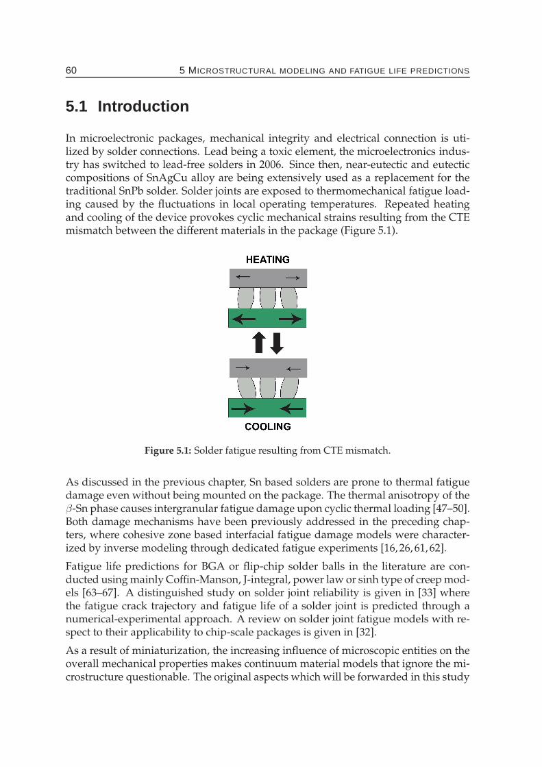
60 5 MICROSTRUCTURAL MODELING AND FATIGUE LIFE PREDICTIONS
5.1 Introduction
In microelectronic packages, mechanical integrity and electrical connection is uti-lized by solder connections. Lead being a toxic element, the microelectronics indus-try has switched to lead-free solders in 2006. Since then, near-eutectic and eutecticcompositions of SnAgCu alloy are being extensively used as a replacement for thetraditional SnPb solder. Solder joints are exposed to thermomechanical fatigue load-ing caused by the fluctuations in local operating temperatures. Repeated heatingand cooling of the device provokes cyclic mechanical strains resulting from the CTEmismatch between the different materials in the package (Figure 5.1).
Figure 5.1: Solder fatigue resulting from CTE mismatch.
As discussed in the previous chapter, Sn based solders are prone to thermal fatiguedamage even without being mounted on the package. The thermal anisotropy of theβ-Sn phase causes intergranular fatigue damage upon cyclic thermal loading [47–50].Both damage mechanisms have been previously addressed in the preceding chap-ters, where cohesive zone based interfacial fatigue damage models were character-ized by inverse modeling through dedicated fatigue experiments [16, 26, 61, 62].
Fatigue life predictions for BGA or flip-chip solder balls in the literature are con-ducted using mainly Coffin-Manson, J-integral, power law or sinh type of creep mod-els [63–67]. A distinguished study on solder joint reliability is given in [33] wherethe fatigue crack trajectory and fatigue life of a solder joint is predicted through anumerical-experimental approach. A review on solder joint fatigue models with re-spect to their applicability to chip-scale packages is given in [32].
As a result of miniaturization, the increasing influence of microscopic entities on theoverall mechanical properties makes continuum material models that ignore the mi-crostructure questionable. The original aspects which will be forwarded in this study
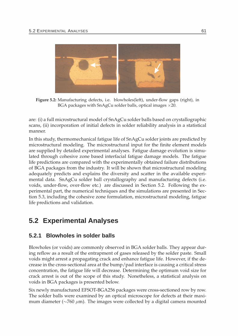
5.2 EXPERIMENTAL ANALYSES 61
Figure 5.2: Manufacturing defects, i.e. blowholes(left), under-flow gaps (right), inBGA packages with SnAgCu solder balls, optical images ×20.
are: (i) a full microstructural model of SnAgCu solder balls based on crystallographicscans, (ii) incorporation of initial defects in solder reliability analysis in a statisticalmanner.
In this study, thermomechanical fatigue life of SnAgCu solder joints are predicted bymicrostructural modeling. The microstructural input for the finite element modelsare supplied by detailed experimental analyses. Fatigue damage evolution is simu-lated through cohesive zone based interfacial fatigue damage models. The fatiguelife predictions are compared with the experimentally obtained failure distributionsof BGA packages from the industry. It will be shown that microstructural modelingadequately predicts and explains the diversity and scatter in the available experi-mental data. SnAgCu solder ball crystallography and manufacturing defects (i.e.voids, under-flow, over-flow etc.) are discussed in Section 5.2. Following the ex-perimental part, the numerical techniques and the simulations are presented in Sec-tion 5.3, including the cohesive zone formulation, microstructural modeling, fatiguelife predictions and validation.
5.2 Experimental Analyses
5.2.1 Blowholes in solder balls
Blowholes (or voids) are commonly observed in BGA solder balls. They appear dur-ing reflow as a result of the entrapment of gases released by the solder paste. Smallvoids might arrest a propagating crack and enhance fatigue life. However, if the de-crease in the cross-sectional area at the bump/pad interface is causing a critical stressconcentration, the fatigue life will decrease. Determining the optimum void size forcrack arrest is out of the scope of this study. Nonetheless, a statistical analysis onvoids in BGA packages is presented below.
Six newly manufactured EFSOT-BGA256 packages were cross-sectioned row by row.The solder balls were examined by an optical microscope for defects at their maxi-mum diameter (∼760 µm). The images were collected by a digital camera mounted
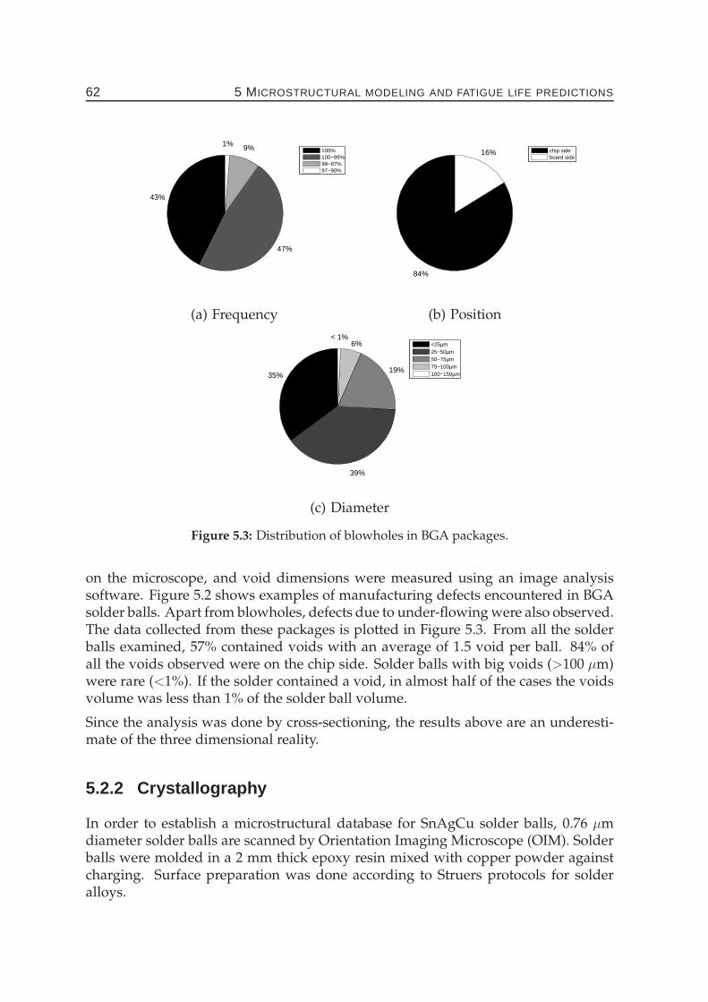
62 5 MICROSTRUCTURAL MODELING AND FATIGUE LIFE PREDICTIONS
43%
47%
9%1%100%100−99%99−97%97−90%
(a) Frequency
84%
16% chip sideboard side
(b) Position
35%
39%
19%
6%< 1%
<25µm25−50µm50−75µm75−100µm100−150µm
(c) Diameter
Figure 5.3: Distribution of blowholes in BGA packages.
on the microscope, and void dimensions were measured using an image analysissoftware. Figure 5.2 shows examples of manufacturing defects encountered in BGAsolder balls. Apart from blowholes, defects due to under-flowing were also observed.The data collected from these packages is plotted in Figure 5.3. From all the solderballs examined, 57% contained voids with an average of 1.5 void per ball. 84% ofall the voids observed were on the chip side. Solder balls with big voids (>100 µm)were rare (<1%). If the solder contained a void, in almost half of the cases the voidsvolume was less than 1% of the solder ball volume.
Since the analysis was done by cross-sectioning, the results above are an underesti-mate of the three dimensional reality.
5.2.2 Crystallography
In order to establish a microstructural database for SnAgCu solder balls, 0.76 µmdiameter solder balls are scanned by Orientation Imaging Microscope (OIM). Solderballs were molded in a 2 mm thick epoxy resin mixed with copper powder againstcharging. Surface preparation was done according to Struers protocols for solderalloys.
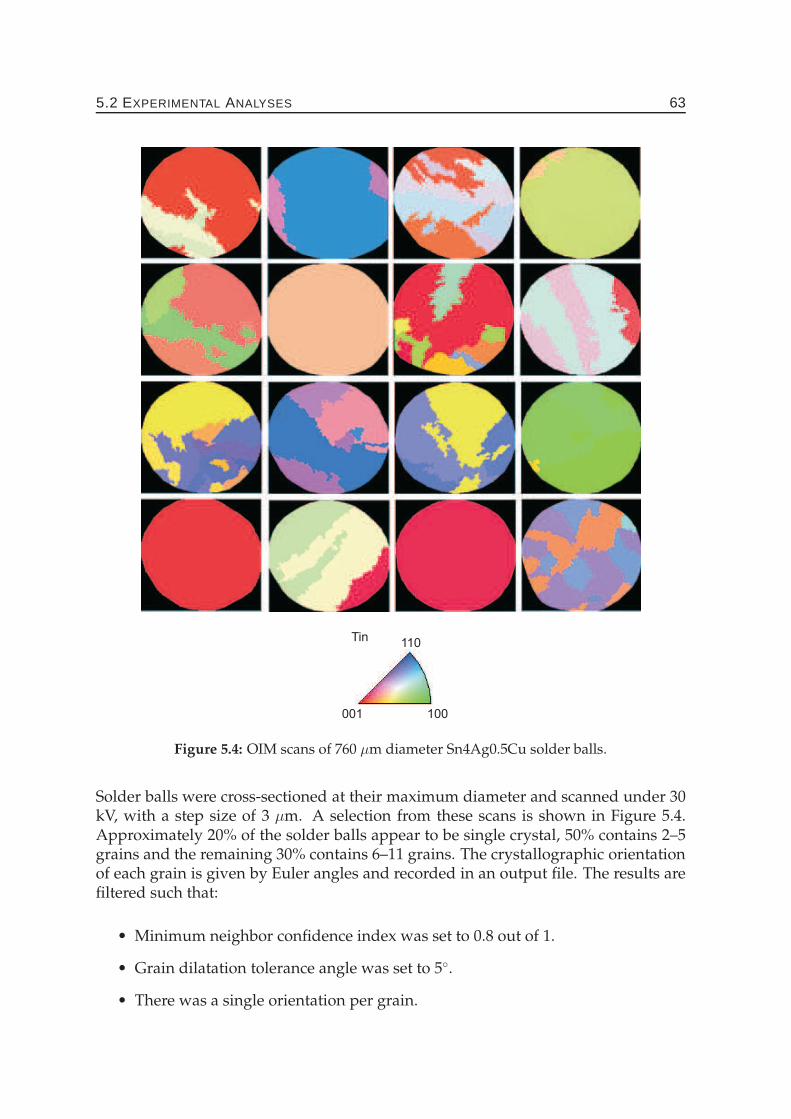
5.2 EXPERIMENTAL ANALYSES 63
Tin110
100001
Figure 5.4: OIM scans of 760 µm diameter Sn4Ag0.5Cu solder balls.
Solder balls were cross-sectioned at their maximum diameter and scanned under 30kV, with a step size of 3 µm. A selection from these scans is shown in Figure 5.4.Approximately 20% of the solder balls appear to be single crystal, 50% contains 2–5grains and the remaining 30% contains 6–11 grains. The crystallographic orientationof each grain is given by Euler angles and recorded in an output file. The results arefiltered such that:
• Minimum neighbor confidence index was set to 0.8 out of 1.
• Grain dilatation tolerance angle was set to 5◦.
• There was a single orientation per grain.
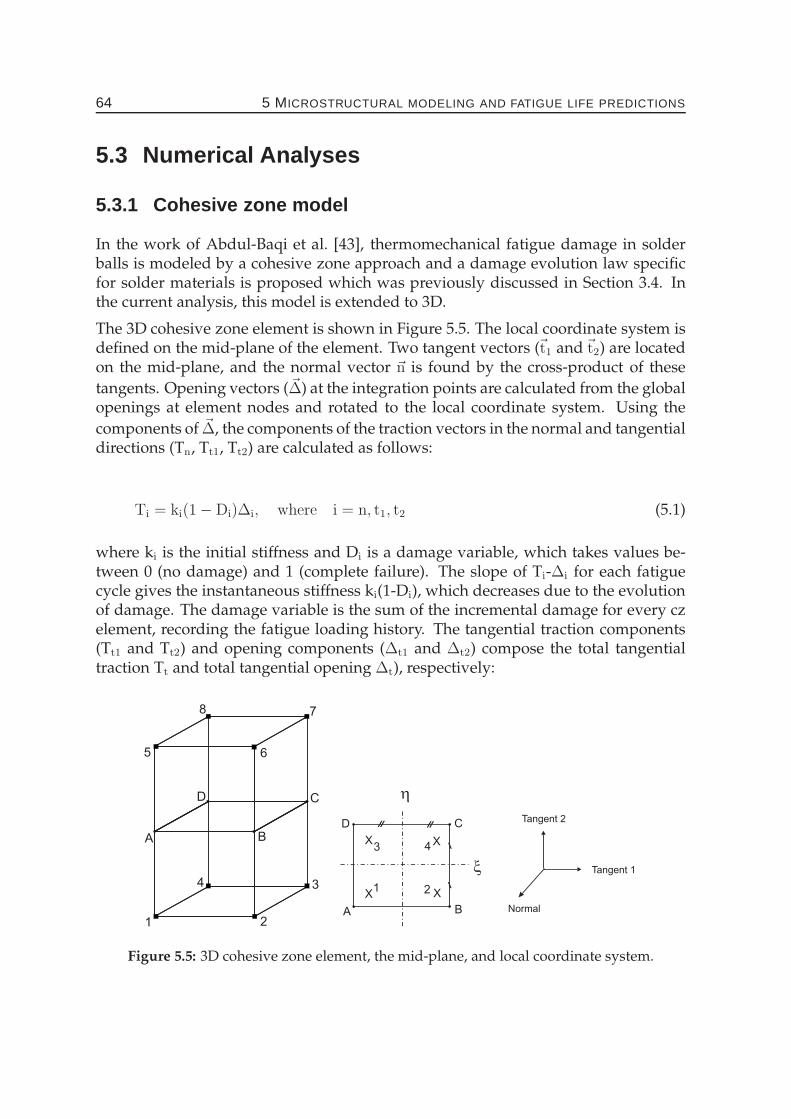
64 5 MICROSTRUCTURAL MODELING AND FATIGUE LIFE PREDICTIONS
5.3 Numerical Analyses
5.3.1 Cohesive zone model
In the work of Abdul-Baqi et al. [43], thermomechanical fatigue damage in solderballs is modeled by a cohesive zone approach and a damage evolution law specificfor solder materials is proposed which was previously discussed in Section 3.4. Inthe current analysis, this model is extended to 3D.
The 3D cohesive zone element is shown in Figure 5.5. The local coordinate system isdefined on the mid-plane of the element. Two tangent vectors (~t1 and~t2) are locatedon the mid-plane, and the normal vector ~n is found by the cross-product of these
tangents. Opening vectors (~∆) at the integration points are calculated from the globalopenings at element nodes and rotated to the local coordinate system. Using the
components of ~∆, the components of the traction vectors in the normal and tangentialdirections (Tn, Tt1, Tt2) are calculated as follows:
Ti = ki(1 − Di)∆i, where i = n, t1, t2 (5.1)
where ki is the initial stiffness and Di is a damage variable, which takes values be-tween 0 (no damage) and 1 (complete failure). The slope of Ti-∆i for each fatiguecycle gives the instantaneous stiffness ki(1-Di), which decreases due to the evolutionof damage. The damage variable is the sum of the incremental damage for every czelement, recording the fatigue loading history. The tangential traction components(Tt1 and Tt2) and opening components (∆t1 and ∆t2) compose the total tangentialtraction Tt and total tangential opening ∆t), respectively:
1 2
34
5 6
78
A B
CD h
x
IIII
I
I
Tangent 1
Tangent 2
NormalA B
CD
X X
X X1 2
3 4
Figure 5.5: 3D cohesive zone element, the mid-plane, and local coordinate system.
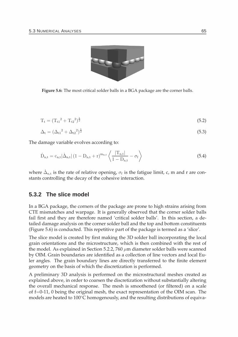
5.3 NUMERICAL ANALYSES 65
Figure 5.6: The most critical solder balls in a BGA package are the corner balls.
Tt = (Tt12 + Tt2
2)1
2 (5.2)
∆t = (∆t12 + ∆t2
2)1
2 (5.3)
The damage variable evolves according to:
Dn,t = cn,t|∆n,t| (1 − Dn,t + r)mn,t
⟨ |Tn,t|1 − Dn,t
− σf
⟩
(5.4)
where ∆n,t is the rate of relative opening, σf is the fatigue limit, c, m and r are con-stants controlling the decay of the cohesive interaction.
5.3.2 The slice model
In a BGA package, the corners of the package are prone to high strains arising fromCTE mismatches and warpage. It is generally observed that the corner solder ballsfail first and they are therefore named ‘critical solder balls’. In this section, a de-tailed damage analysis on the corner solder ball and the top and bottom constituents(Figure 5.6) is conducted. This repetitive part of the package is termed as a ‘slice’.
The slice model is created by first making the 3D solder ball incorporating the localgrain orientations and the microstructure, which is then combined with the rest ofthe model. As explained in Section 5.2.2, 760 µm diameter solder balls were scannedby OIM. Grain boundaries are identified as a collection of line vectors and local Eu-ler angles. The grain boundary lines are directly transferred to the finite elementgeometry on the basis of which the discretization is performed.
A preliminary 3D analysis is performed on the microstructural meshes created asexplained above, in order to coarsen the discretization without substantially alteringthe overall mechanical response. The mesh is smoothened (or filtered) on a scaleof f=0-11, 0 being the original mesh, the exact representation of the OIM scan. Themodels are heated to 100◦C homogenously, and the resulting distributions of equiva-
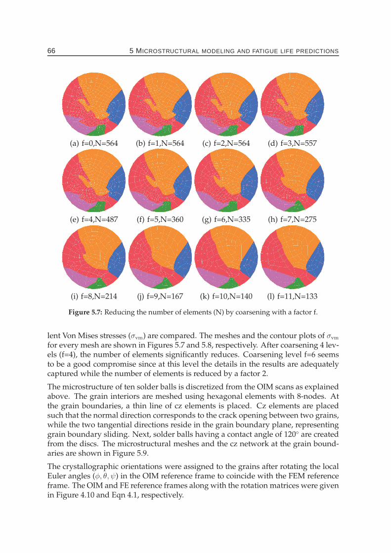
66 5 MICROSTRUCTURAL MODELING AND FATIGUE LIFE PREDICTIONS
(a) f=0,N=564 (b) f=1,N=564 (c) f=2,N=564 (d) f=3,N=557
(e) f=4,N=487 (f) f=5,N=360 (g) f=6,N=335 (h) f=7,N=275
(i) f=8,N=214 (j) f=9,N=167 (k) f=10,N=140 (l) f=11,N=133
Figure 5.7: Reducing the number of elements (N) by coarsening with a factor f.
lent Von Mises stresses (σvm) are compared. The meshes and the contour plots of σvm
for every mesh are shown in Figures 5.7 and 5.8, respectively. After coarsening 4 lev-els (f=4), the number of elements significantly reduces. Coarsening level f=6 seemsto be a good compromise since at this level the details in the results are adequatelycaptured while the number of elements is reduced by a factor 2.
The microstructure of ten solder balls is discretized from the OIM scans as explainedabove. The grain interiors are meshed using hexagonal elements with 8-nodes. Atthe grain boundaries, a thin line of cz elements is placed. Cz elements are placedsuch that the normal direction corresponds to the crack opening between two grains,while the two tangential directions reside in the grain boundary plane, representinggrain boundary sliding. Next, solder balls having a contact angle of 120◦ are createdfrom the discs. The microstructural meshes and the cz network at the grain bound-aries are shown in Figure 5.9.
The crystallographic orientations were assigned to the grains after rotating the localEuler angles (φ, θ, ψ) in the OIM reference frame to coincide with the FEM referenceframe. The OIM and FE reference frames along with the rotation matrices were givenin Figure 4.10 and Eqn 4.1, respectively.
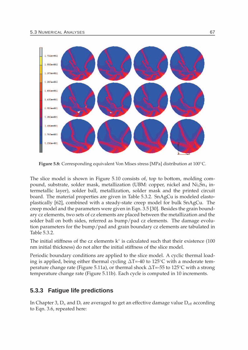
5.3 NUMERICAL ANALYSES 67
Figure 5.8: Corresponding equivalent Von Mises stress [MPa] distribution at 100◦C.
The slice model is shown in Figure 5.10 consists of, top to bottom, molding com-pound, substrate, solder mask, metallization (UBM: copper, nickel and Ni3Sn4 in-termetallic layer), solder ball, metallization, solder mask and the printed circuitboard. The material properties are given in Table 5.3.2. SnAgCu is modeled elasto-plastically [62], combined with a steady-state creep model for bulk SnAgCu. Thecreep model and the parameters were given in Eqn. 3.5 [30]. Besides the grain bound-ary cz elements, two sets of cz elements are placed between the metallization and thesolder ball on both sides, referred as bump/pad cz elements. The damage evolu-tion parameters for the bump/pad and grain boundary cz elements are tabulated inTable 5.3.2.
The initial stiffness of the cz elements k◦ is calculated such that their existence (100nm initial thickness) do not alter the initial stiffness of the slice model.
Periodic boundary conditions are applied to the slice model. A cyclic thermal load-ing is applied, being either thermal cycling ∆T=-40 to 125◦C with a moderate tem-perature change rate (Figure 5.11a), or thermal shock ∆T=-55 to 125◦C with a strongtemperature change rate (Figure 5.11b). Each cycle is computed in 10 increments.
5.3.3 Fatigue life predictions
In Chapter 3, Dn and Dt are averaged to get an effective damage value Deff accordingto Eqn. 3.6, repeated here:

68 5 MICROSTRUCTURAL MODELING AND FATIGUE LIFE PREDICTIONS
(a) Disc nr.1
(b) Disc nr.3
(c) Disc nr.4
(d) Disc nr.5

5.3 NUMERICAL ANALYSES 69
(e) Disc nr.6
(f) Disc nr.8
(g) Disc nr.9
(h) Disc nr.10
Figure 5.9: Examples of microstructural meshes.
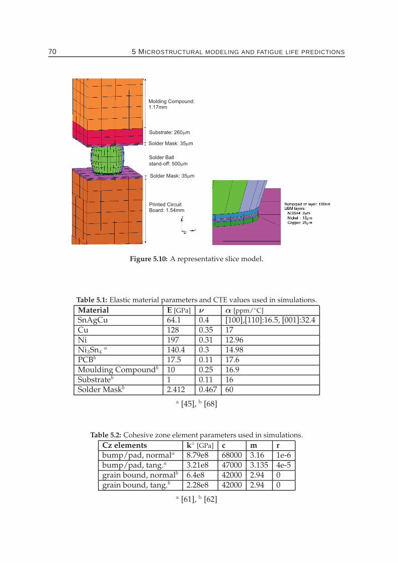
70 5 MICROSTRUCTURAL MODELING AND FATIGUE LIFE PREDICTIONS
Molding Compound:1.17mm
Substrate: 260 mm
Solder Mask: 35 mm
Solder Mask: 35 mm
Printed CircuitBoard: 1.54mm
Solder Ball
stand-off: 500 mm
Figure 5.10: A representative slice model.
Table 5.1: Elastic material parameters and CTE values used in simulations.
Material E [GPa] ν α [ppm/◦C]
SnAgCu 64.1 0.4 [100],[110]:16.5, [001]:32.4Cu 128 0.35 17Ni 197 0.31 12.96Ni3Sn4
a 140.4 0.3 14.98PCBb 17.5 0.11 17.6Moulding Compoundb 10 0.25 16.9Substrateb 1 0.11 16Solder Maskb 2.412 0.467 60
a [45], b [68]
Table 5.2: Cohesive zone element parameters used in simulations.
Cz elements k◦ [GPa] c m r
bump/pad, normala 8.79e8 68000 3.16 1e-6bump/pad, tang.a 3.21e8 47000 3.135 4e-5grain bound, normalb 6.4e8 42000 2.94 0grain bound, tang.b 2.28e8 42000 2.94 0
a [61], b [62]
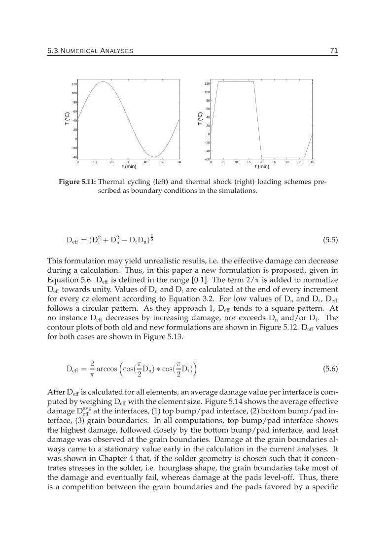
5.3 NUMERICAL ANALYSES 71
0 10 20 30 40 50 60
−40
−20
0
20
40
60
80
100
120
t (min)
T (°
C)
0 5 10 15 20 25 30 35 40−60
−40
−20
0
20
40
60
80
100
120
t (min)
T (°
C)
Figure 5.11: Thermal cycling (left) and thermal shock (right) loading schemes pre-scribed as boundary conditions in the simulations.
Deff = (D2t + D2
n − DtDn)1
2 (5.5)
This formulation may yield unrealistic results, i.e. the effective damage can decreaseduring a calculation. Thus, in this paper a new formulation is proposed, given inEquation 5.6. Deff is defined in the range [0 1]. The term 2/π is added to normalizeDeff towards unity. Values of Dn and Dt are calculated at the end of every incrementfor every cz element according to Equation 3.2. For low values of Dn and Dt, Deff
follows a circular pattern. As they approach 1, Deff tends to a square pattern. Atno instance Deff decreases by increasing damage, nor exceeds Dn and/or Dt. Thecontour plots of both old and new formulations are shown in Figure 5.12. Deff valuesfor both cases are shown in Figure 5.13.
Deff =2
πarccos
(
cos(π
2Dn) ∗ cos(
π
2Dt)
)
(5.6)
After Deff is calculated for all elements, an average damage value per interface is com-puted by weighing Deff with the element size. Figure 5.14 shows the average effectivedamage Davg
eff at the interfaces, (1) top bump/pad interface, (2) bottom bump/pad in-terface, (3) grain boundaries. In all computations, top bump/pad interface showsthe highest damage, followed closely by the bottom bump/pad interface, and leastdamage was observed at the grain boundaries. Damage at the grain boundaries al-ways came to a stationary value early in the calculation in the current analyses. Itwas shown in Chapter 4 that, if the solder geometry is chosen such that it concen-trates stresses in the solder, i.e. hourglass shape, the grain boundaries take most ofthe damage and eventually fail, whereas damage at the pads level-off. Thus, thereis a competition between the grain boundaries and the pads favored by a specific
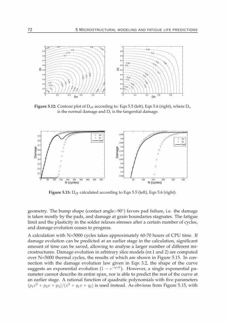
72 5 MICROSTRUCTURAL MODELING AND FATIGUE LIFE PREDICTIONS
0.05
0.1
0.150.2 0.25
0.3
0.35
0.4
0.45
0.5
0.55
0.6
0.65
0.7
0.75
0.8
0.85
0.9 0.9
0.9
0.95 0.95
0.95
Dn
Dt
0 0.2 0.4 0.6 0.8 10
0.1
0.2
0.3
0.4
0.5
0.6
0.7
0.8
0.9
1
0.1
0.15 0.2
0.25
0.30.35
0.40.45
0.5
0.55
0.60.65
0.7
0.75
0.8 0.85
0.9
0.95
Dn
Dt
0 0.2 0.4 0.6 0.8 10
0.1
0.2
0.3
0.4
0.5
0.6
0.7
0.8
0.9
1
Figure 5.12: Contour plot of Deff according to: Eqn 5.5 (left), Eqn 5.6 (right), where Dn
is the normal damage and Dt is the tangential damage.
0 50 100 150 200 250 300 350 400 4500
0.1
0.2
0.3
0.4
0.5
0.6
0.7
0.8
0.9
N (cycles)
Dam
age
DnDtDeff
50 100 150 200 250 300
0.45
0.5
0.55
0.6
0.65
0.7
0.75
0.8
0.85
0.9
0.95
N (cycles)
Dam
age
DnDtDeff
Figure 5.13: Deff calculated according to Eqn 5.5 (left), Eqn 5.6 (right).
geometry. The bump shape (contact angle>90◦) favors pad failure, i.e. the damageis taken mostly by the pads, and damage at grain boundaries stagnates. The fatiguelimit and the plasticity in the solder relaxes stresses after a certain number of cycles,and damage evolution ceases to progress.
A calculation with N=5000 cycles takes approximately 60-70 hours of CPU time. Ifdamage evolution can be predicted at an earlier stage in the calculation, significantamount of time can be saved, allowing to analyse a larger number of different mi-crostructures. Damage evolution in arbitrary slice models (nr.1 and 2) are computedover N=5000 thermal cycles, the results of which are shown in Figure 5.15. In con-nection with the damage evolution law given in Eqn 3.2, the shape of the curvesuggests an exponential evolution (1 − e−a∗N ). However, a single exponential pa-rameter cannot describe its entire span, nor is able to predict the rest of the curve atan earlier stage. A rational function of quadratic polynomials with five parameters(p1x
2 + p2x + p3)/(x2 + q1x + q2) is used instead. As obvious from Figure 5.15, with
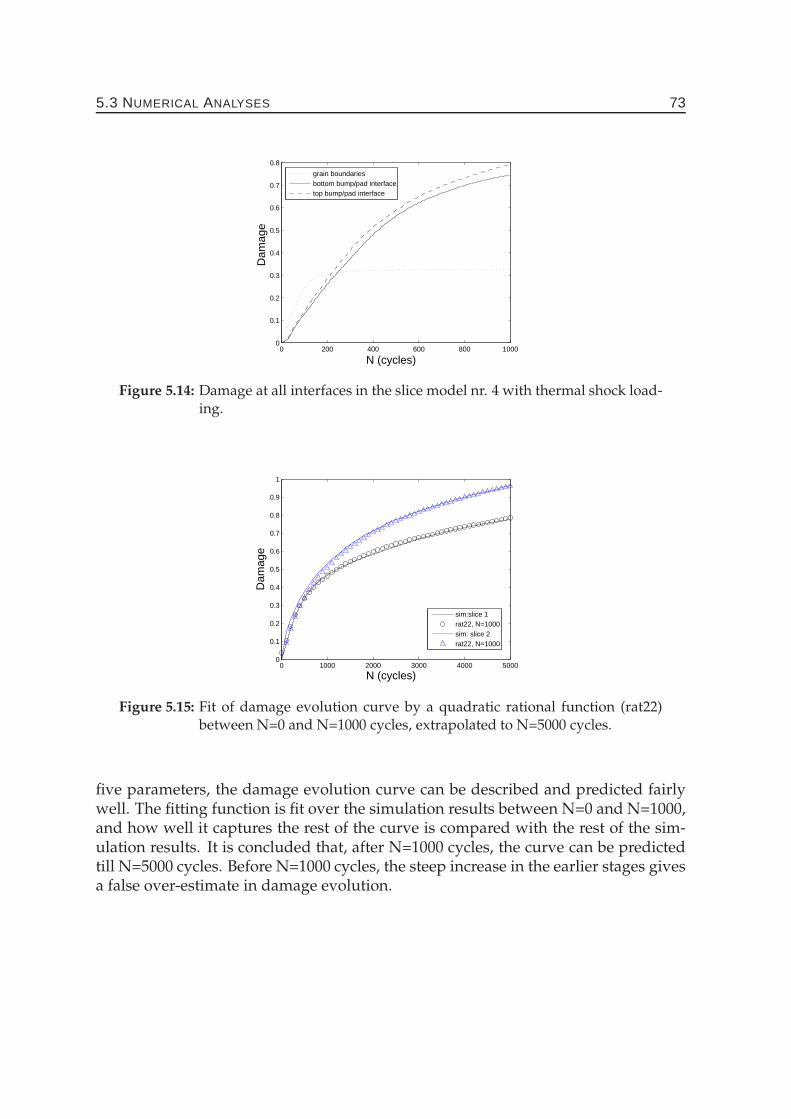
5.3 NUMERICAL ANALYSES 73
0 200 400 600 800 10000
0.1
0.2
0.3
0.4
0.5
0.6
0.7
0.8
N (cycles)
Dam
age
grain boundariesbottom bump/pad interfacetop bump/pad interface
Figure 5.14: Damage at all interfaces in the slice model nr. 4 with thermal shock load-ing.
0 1000 2000 3000 4000 50000
0.1
0.2
0.3
0.4
0.5
0.6
0.7
0.8
0.9
1
N (cycles)
Dam
age
sim:slice 1rat22, N=1000sim: slice 2rat22, N=1000
Figure 5.15: Fit of damage evolution curve by a quadratic rational function (rat22)between N=0 and N=1000 cycles, extrapolated to N=5000 cycles.
five parameters, the damage evolution curve can be described and predicted fairlywell. The fitting function is fit over the simulation results between N=0 and N=1000,and how well it captures the rest of the curve is compared with the rest of the sim-ulation results. It is concluded that, after N=1000 cycles, the curve can be predictedtill N=5000 cycles. Before N=1000 cycles, the steep increase in the earlier stages givesa false over-estimate in damage evolution.
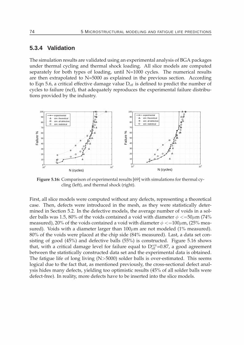
74 5 MICROSTRUCTURAL MODELING AND FATIGUE LIFE PREDICTIONS
5.3.4 Validation
The simulation results are validated using an experimental analysis of BGA packagesunder thermal cycling and thermal shock loading. All slice models are computedseparately for both types of loading, until N=1000 cycles. The numerical resultsare then extrapolated to N=5000 as explained in the previous section. Accordingto Eqn 5.6, a critical effective damage value Deff is defined to predict the number ofcycles to failure (ncf), that adequately reproduces the experimental failure distribu-tions provided by the industry.
103
104
0
10
20
30
40
50
60
70
80
90
100
N (cycles)
Fai
lure
%
experimentalsim: theoreticalsim: all defectivesim: statistical
103
104
0
10
20
30
40
50
60
70
80
90
100
N (cycles)
Fai
lure
%
experimentalsim: theoreticalsim: all defectivesim: statistical
Figure 5.16: Comparison of experimental results [69] with simulations for thermal cy-cling (left), and thermal shock (right).
First, all slice models were computed without any defects, representing a theoreticalcase. Then, defects were introduced in the mesh, as they were statistically deter-mined in Section 5.2. In the defective models, the average number of voids in a sol-der balls was 1.5, 80% of the voids contained a void with diameter φ <=50µm (74%measured), 20% of the voids contained a void with diameter φ <=100µm, (25% mea-sured). Voids with a diameter larger than 100µm are not modeled (1% measured).80% of the voids were placed at the chip side (84% measured). Last, a data set con-sisting of good (45%) and defective balls (55%) is constructed. Figure 5.16 showsthat, with a critical damage level for failure equal to Dcrit
eff =0.87, a good agreementbetween the statistically constructed data set and the experimental data is obtained.The fatigue life of long living (N>5000) solder balls is over-estimated. This seemslogical due to the fact that, as mentioned previously, the cross-sectional defect anal-ysis hides many defects, yielding too optimistic results (45% of all solder balls weredefect-free). In reality, more defects have to be inserted into the slice models.
5.4 CONCLUSIONS 75
5.4 Conclusions
In this study, the thermomechanical reliability of lead-free BGA solder balls is inves-tigated by microstructural modeling. Three dimensional solder joints are simulatedincorporating the microstructure, local orientations and initial defects, which werenot handled in the literature before. The fatigue life is determined using cohesivezone based damage models for bump/pad crack propagation and intergranular fa-tigue damage. It is seen that microstructural modeling allows to predict and under-stand the scatter in the solder ball fatigue life observed in reality. The methodologyused in this study will be used to assess solder interconnect reliability under differentgeometrical and/or loading conditions, especially regarding the effect of miniatur-ization on solder reliability.
The following conclusions are drawn from the current analyses:
• Manufacturing defects in EFSOT-BGA256 packages are optically examined.57% of all solder balls examined contained voids, on average 1.5 void per ball.84% of all the voids observed were on the chip side. Solder balls with big voids(>100 µm) were rare (<1%). If the solder contained a void, almost half of thecases the voids volume was less than 1% of the solder ball volume.
• 760 µm SnAgCu solder balls from a single manufacturer are examined for theircrystallographic structure. Approximately 20% of the solder balls were singlecrystal, 50% contained 2–5 grains, remaining 30% contained 6–11 grains.
• Microstructural meshes of 10 solder balls are created. At the grain boundariesand bump/pad interfaces, cohesive zone elements are placed. The thermalfatigue damage evolution at certain interfaces is monitored through these czelements. Fatigue lives of the solder balls are predicted under thermal cycling(∆T=-40 to 125◦C), or thermal shock (∆T=-55 to 125◦C) loading.
• The numerical results are compared with experimental fatigue life analyses ob-tained from the industry. A critical effective damage value for failure for aninterface is determined. After inserting initial defects into the models, an ade-quate agreement between the numerical analyses and the experimental valuesis achieved.


CHAPTER SIX
Impact of miniaturization on solderreliability
Abstract
The solder ball model developed in this thesis is extended in order to predict theeffect of solder ball size and geometry on the interconnect reliability, which is par-ticularly important for miniaturization. In BGA packages the pitch size is correlatedto the solder ball diameter and the stand-off height. In this study, pitch size is alsocorrelated to the contact angle between the solder and the substrate. Finite elementslice models are constructed separately for five contact angles with different stand-off heights. Bump/pad interfaces and the bulk solder are analyzed by determiningplastic strain accumulation and equivalent Von Mises stresses resulting from ther-mal loading. Geometrical and microstructural criticality are quantified by describinga geometry factor and a microstructure factor. The geometry factor is related to theshape of the solder, and the microstructure factor is related to the grain boundaryarea and the mismatch of local crystallographic orientations at the grain boundaries.The influence of these two factors on solder reliability is discussed.
77
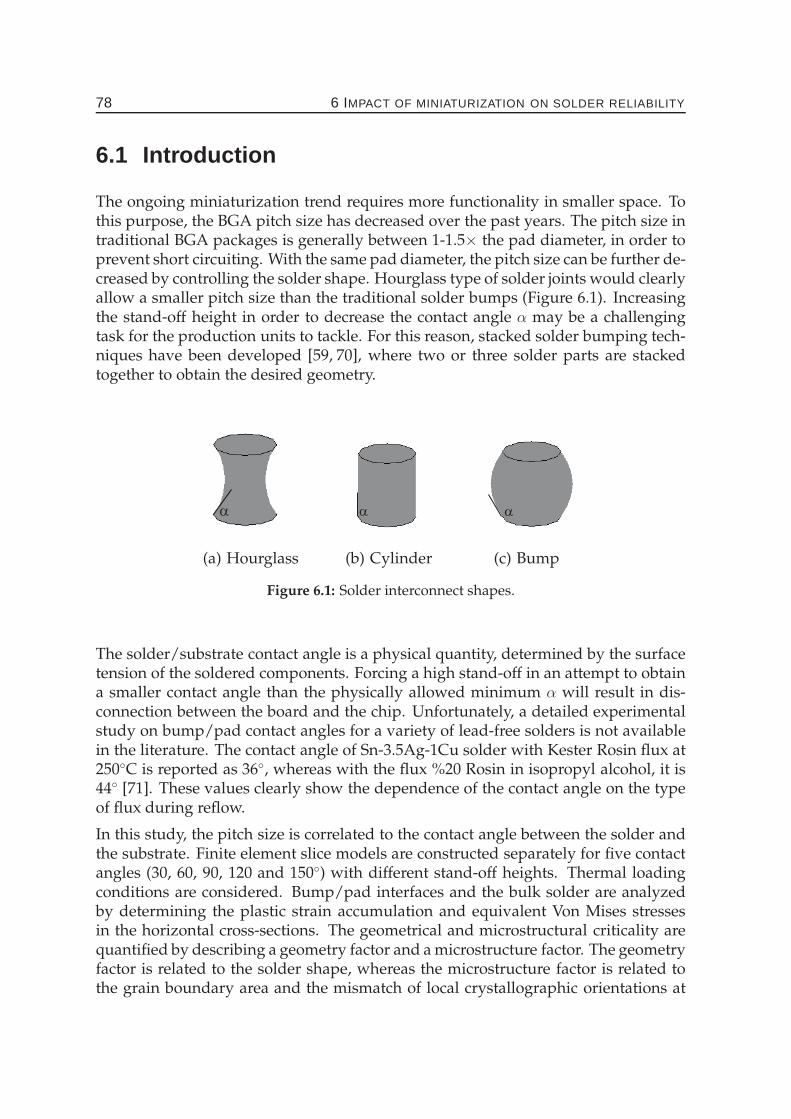
78 6 IMPACT OF MINIATURIZATION ON SOLDER RELIABILITY
6.1 Introduction
The ongoing miniaturization trend requires more functionality in smaller space. Tothis purpose, the BGA pitch size has decreased over the past years. The pitch size intraditional BGA packages is generally between 1-1.5× the pad diameter, in order toprevent short circuiting. With the same pad diameter, the pitch size can be further de-creased by controlling the solder shape. Hourglass type of solder joints would clearlyallow a smaller pitch size than the traditional solder bumps (Figure 6.1). Increasingthe stand-off height in order to decrease the contact angle α may be a challengingtask for the production units to tackle. For this reason, stacked solder bumping tech-niques have been developed [59, 70], where two or three solder parts are stackedtogether to obtain the desired geometry.
a
(a) Hourglass
a
(b) Cylinder
a
(c) Bump
Figure 6.1: Solder interconnect shapes.
The solder/substrate contact angle is a physical quantity, determined by the surfacetension of the soldered components. Forcing a high stand-off in an attempt to obtaina smaller contact angle than the physically allowed minimum α will result in dis-connection between the board and the chip. Unfortunately, a detailed experimentalstudy on bump/pad contact angles for a variety of lead-free solders is not availablein the literature. The contact angle of Sn-3.5Ag-1Cu solder with Kester Rosin flux at250◦C is reported as 36◦, whereas with the flux %20 Rosin in isopropyl alcohol, it is44◦ [71]. These values clearly show the dependence of the contact angle on the typeof flux during reflow.
In this study, the pitch size is correlated to the contact angle between the solder andthe substrate. Finite element slice models are constructed separately for five contactangles (30, 60, 90, 120 and 150◦) with different stand-off heights. Thermal loadingconditions are considered. Bump/pad interfaces and the bulk solder are analyzedby determining the plastic strain accumulation and equivalent Von Mises stressesin the horizontal cross-sections. The geometrical and microstructural criticality arequantified by describing a geometry factor and a microstructure factor. The geometryfactor is related to the solder shape, whereas the microstructure factor is related tothe grain boundary area and the mismatch of local crystallographic orientations at
6.2 SIMULATIONS 79
the grain boundaries. The influence of these two factors on damage evolution isdiscussed in a miniaturization context.
6.2 Simulations
BGA package slice models with five different contact angles α = 30, 60, 90, 120 and150◦ are created. The slice models shown in Figure 6.2 consist of, top to bottom,molding compound, solder mask, intermetallic compound, solder ball, intermetalliccompound, solder mask and the printed circuit board. The UBM layers Cu/Ni(Au)are situated in the solder mask, approximating the physical reality better than theslice models shown in Section 5.3.2. The material properties are assigned as givenin Table 5.3.2, except the printed circuit board. Here orthotropic elastic and thermalmaterial properties are used, as listed in Table 6.1 [72].
Table 6.1: Orthotropic elastic material properties for the FR-4 PCB [72].
Direction E [GPa] ν α [ppm]
x 25.2 0.39 (xy) 14.5y 25.2 0.11 (yz) 14.5z 11 0.11 (xz) 63.5
In order to separate the effect of size and geometry from the microstructure, the sol-der joints in the slice models are first considered as single crystals. Periodic bound-ary conditions are applied to (xy) and (yz) edge planes. A monotonously increasingthermal load is applied from T=25 to 125◦C homogenously, in 10 increments. Twodifferent stand-off height values are considered for all contact angles being h = 234and 300 µm, where the solder pad diameter is fixed to 250 µm.
6.2.1 Geometrical Considerations
A geometry factor GF is next proposed allowing to compare the criticality imposedby the solder geometry (Eqn. 6.1):
GF =
(
dmid
h
)1
2
V−1
3 (6.1)
where h is the stand-off, dmid is the diameter of solder joint at h/2 and V is the to-tal solder volume. According to this relationship, the GF values calculated for theseveral solder shapes discussed are tabulated in Table 6.2.
Unlike the previous chapters, cohesive zone elements are not used in the present
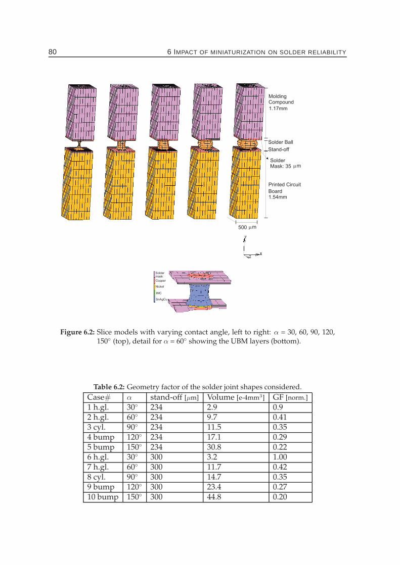
80 6 IMPACT OF MINIATURIZATION ON SOLDER RELIABILITY
MoldingCompound
1.17mm
mmSolderMask: 35
Printed Circuit
Board1.54mm
Solder Ball
Stand-off
mm500
Soldermask
Copper
Nickel
IMC
SnAgCu
Figure 6.2: Slice models with varying contact angle, left to right: α = 30, 60, 90, 120,150◦ (top), detail for α = 60◦ showing the UBM layers (bottom).
Table 6.2: Geometry factor of the solder joint shapes considered.
Case# α stand-off [µm] Volume [e-4mm3] GF [norm.]
1 h.gl. 30◦ 234 2.9 0.92 h.gl. 60◦ 234 9.7 0.413 cyl. 90◦ 234 11.5 0.354 bump 120◦ 234 17.1 0.295 bump 150◦ 234 30.8 0.226 h.gl. 30◦ 300 3.2 1.007 h.gl. 60◦ 300 11.7 0.428 cyl. 90◦ 300 14.7 0.359 bump 120◦ 300 23.4 0.2710 bump 150◦ 300 44.8 0.20
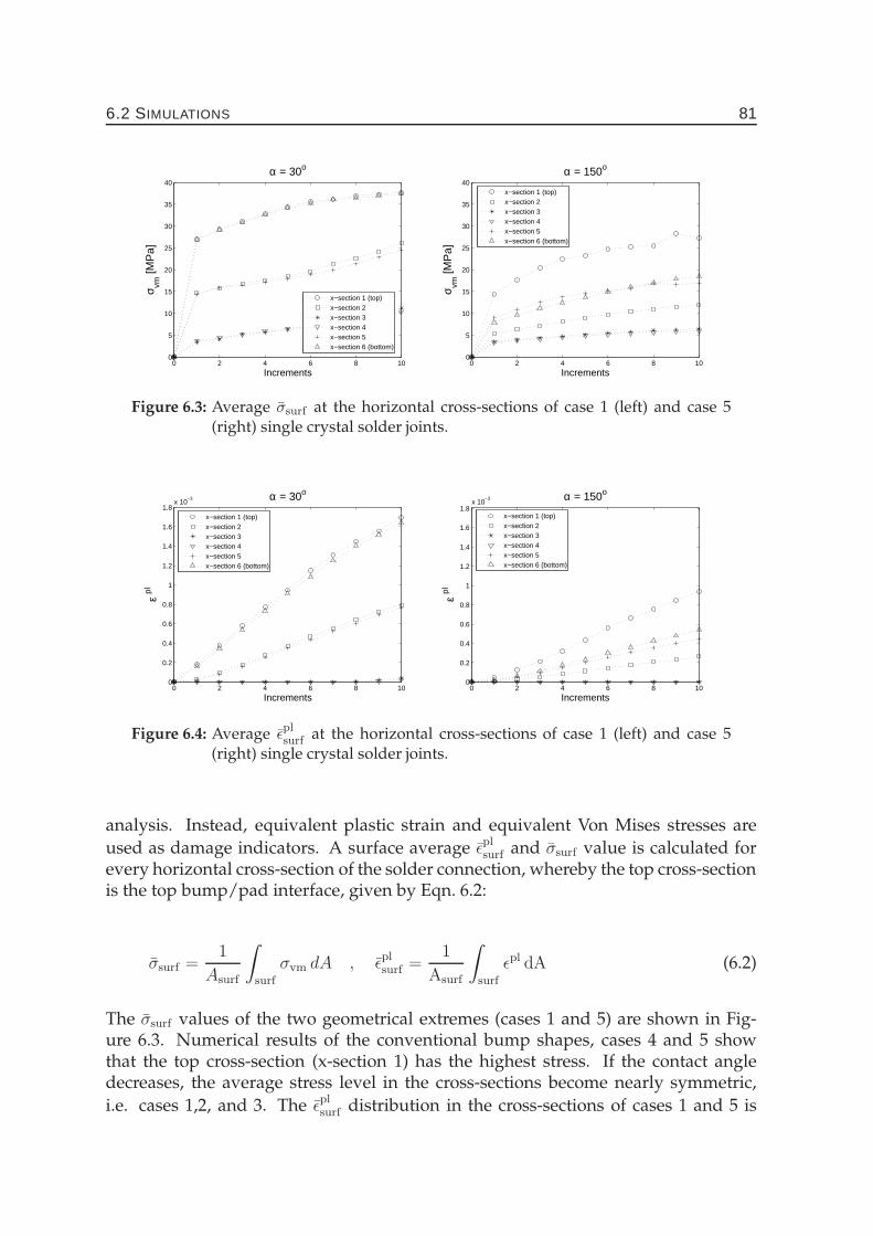
6.2 SIMULATIONS 81
0 2 4 6 8 100
5
10
15
20
25
30
35
40
Increments
σ vm [M
Pa]
α = 30ο
x−section 1 (top)x−section 2x−section 3 x−section 4x−section 5x−section 6 (bottom)
0 2 4 6 8 100
5
10
15
20
25
30
35
40
Increments
σ vm [M
Pa]
α = 150ο
x−section 1 (top)x−section 2x−section 3x−section 4x−section 5x−section 6 (bottom)
Figure 6.3: Average σsurf at the horizontal cross-sections of case 1 (left) and case 5(right) single crystal solder joints.
0 2 4 6 8 100
0.2
0.4
0.6
0.8
1
1.2
1.4
1.6
1.8x 10
−3
Increments
ε pl
α = 30ο
x−section 1 (top)x−section 2x−section 3x−section 4x−section 5x−section 6 (bottom)
0 2 4 6 8 100
0.2
0.4
0.6
0.8
1
1.2
1.4
1.6
1.8x 10
−3
Increments
ε pl
α = 150ο
x−section 1 (top)x−section 2x−section 3x−section 4x−section 5x−section 6 (bottom)
Figure 6.4: Average ǫplsurf at the horizontal cross-sections of case 1 (left) and case 5
(right) single crystal solder joints.
analysis. Instead, equivalent plastic strain and equivalent Von Mises stresses are
used as damage indicators. A surface average ǫplsurf and σsurf value is calculated for
every horizontal cross-section of the solder connection, whereby the top cross-sectionis the top bump/pad interface, given by Eqn. 6.2:
σsurf =1
Asurf
∫
surf
σvm dA , ǫplsurf =
1
Asurf
∫
surf
ǫpl dA (6.2)
The σsurf values of the two geometrical extremes (cases 1 and 5) are shown in Fig-ure 6.3. Numerical results of the conventional bump shapes, cases 4 and 5 showthat the top cross-section (x-section 1) has the highest stress. If the contact angledecreases, the average stress level in the cross-sections become nearly symmetric,
i.e. cases 1,2, and 3. The ǫplsurf distribution in the cross-sections of cases 1 and 5 is
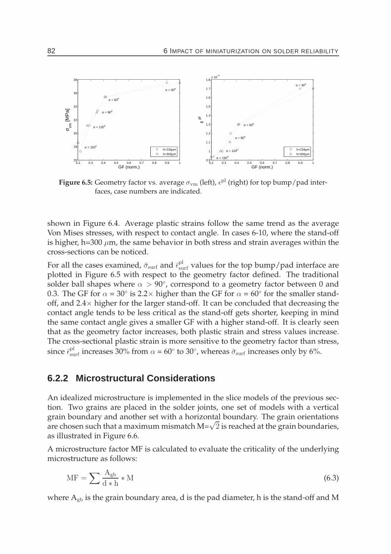
82 6 IMPACT OF MINIATURIZATION ON SOLDER RELIABILITY
0.2 0.3 0.4 0.5 0.6 0.7 0.8 0.9 126
28
30
32
34
36
38
GF (norm.)
σ vm [M
Pa]
α = 30ο
α = 60ο
α = 90ο
α = 120ο
α = 150οh=234µm
h=300µm
0.2 0.3 0.4 0.5 0.6 0.7 0.8 0.9 10.9
1
1.1
1.2
1.3
1.4
1.5
1.6
1.7
1.8x 10
−3
GF (norm.)
ε pl
α = 30ο
α = 60ο
α = 90ο
α = 120ο
α = 150ο
h=234µm
h=300µm
Figure 6.5: Geometry factor vs. average σvm (left), ǫpl (right) for top bump/pad inter-faces, case numbers are indicated.
shown in Figure 6.4. Average plastic strains follow the same trend as the averageVon Mises stresses, with respect to contact angle. In cases 6-10, where the stand-offis higher, h=300 µm, the same behavior in both stress and strain averages within thecross-sections can be noticed.
For all the cases examined, σsurf and ǫplsurf values for the top bump/pad interface are
plotted in Figure 6.5 with respect to the geometry factor defined. The traditionalsolder ball shapes where α > 90◦, correspond to a geometry factor between 0 and0.3. The GF for α = 30◦ is 2.2× higher than the GF for α = 60◦ for the smaller stand-off, and 2.4× higher for the larger stand-off. It can be concluded that decreasing thecontact angle tends to be less critical as the stand-off gets shorter, keeping in mindthe same contact angle gives a smaller GF with a higher stand-off. It is clearly seenthat as the geometry factor increases, both plastic strain and stress values increase.The cross-sectional plastic strain is more sensitive to the geometry factor than stress,
since ǫplsurf increases 30% from α = 60◦ to 30◦, whereas σsurf increases only by 6%.
6.2.2 Microstructural Considerations
An idealized microstructure is implemented in the slice models of the previous sec-tion. Two grains are placed in the solder joints, one set of models with a verticalgrain boundary and another set with a horizontal boundary. The grain orientationsare chosen such that a maximum mismatch M=
√2 is reached at the grain boundaries,
as illustrated in Figure 6.6.
A microstructure factor MF is calculated to evaluate the criticality of the underlyingmicrostructure as follows:
MF =∑ Agb
d ∗ h∗ M (6.3)
where Agb is the grain boundary area, d is the pad diameter, h is the stand-off and M
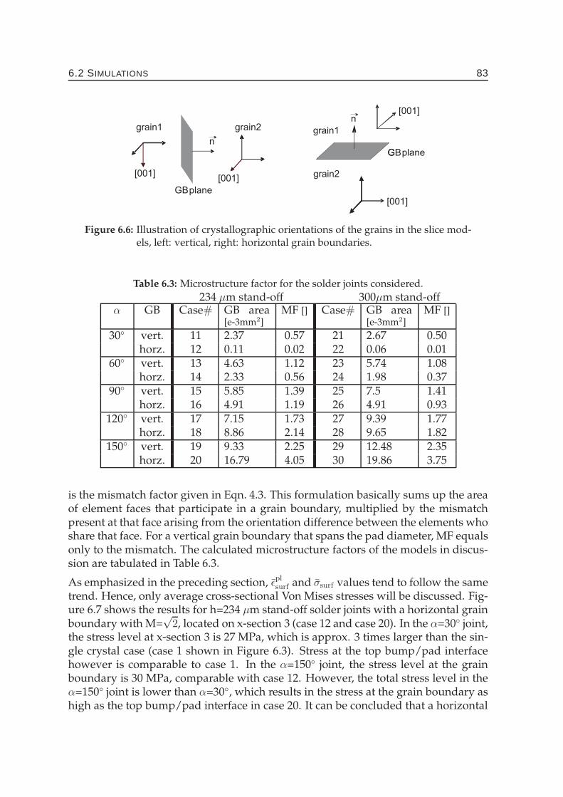
6.2 SIMULATIONS 83
grain1 grain2
GBplane
grain1
grain2
GBplaneG
n
[001][001]
[001]
[001]
n
Figure 6.6: Illustration of crystallographic orientations of the grains in the slice mod-els, left: vertical, right: horizontal grain boundaries.
Table 6.3: Microstructure factor for the solder joints considered.
234 µm stand-off 300µm stand-offα GB Case# GB area
[e-3mm2]MF [] Case# GB area
[e-3mm2]MF []
30◦ vert. 11 2.37 0.57 21 2.67 0.50horz. 12 0.11 0.02 22 0.06 0.01
60◦ vert. 13 4.63 1.12 23 5.74 1.08horz. 14 2.33 0.56 24 1.98 0.37
90◦ vert. 15 5.85 1.39 25 7.5 1.41horz. 16 4.91 1.19 26 4.91 0.93
120◦ vert. 17 7.15 1.73 27 9.39 1.77horz. 18 8.86 2.14 28 9.65 1.82
150◦ vert. 19 9.33 2.25 29 12.48 2.35horz. 20 16.79 4.05 30 19.86 3.75
is the mismatch factor given in Eqn. 4.3. This formulation basically sums up the areaof element faces that participate in a grain boundary, multiplied by the mismatchpresent at that face arising from the orientation difference between the elements whoshare that face. For a vertical grain boundary that spans the pad diameter, MF equalsonly to the mismatch. The calculated microstructure factors of the models in discus-sion are tabulated in Table 6.3.
As emphasized in the preceding section, ǫplsurf and σsurf values tend to follow the same
trend. Hence, only average cross-sectional Von Mises stresses will be discussed. Fig-ure 6.7 shows the results for h=234 µm stand-off solder joints with a horizontal grainboundary with M=
√2, located on x-section 3 (case 12 and case 20). In the α=30◦ joint,
the stress level at x-section 3 is 27 MPa, which is approx. 3 times larger than the sin-gle crystal case (case 1 shown in Figure 6.3). Stress at the top bump/pad interfacehowever is comparable to case 1. In the α=150◦ joint, the stress level at the grainboundary is 30 MPa, comparable with case 12. However, the total stress level in theα=150◦ joint is lower than α=30◦, which results in the stress at the grain boundary ashigh as the top bump/pad interface in case 20. It can be concluded that a horizontal
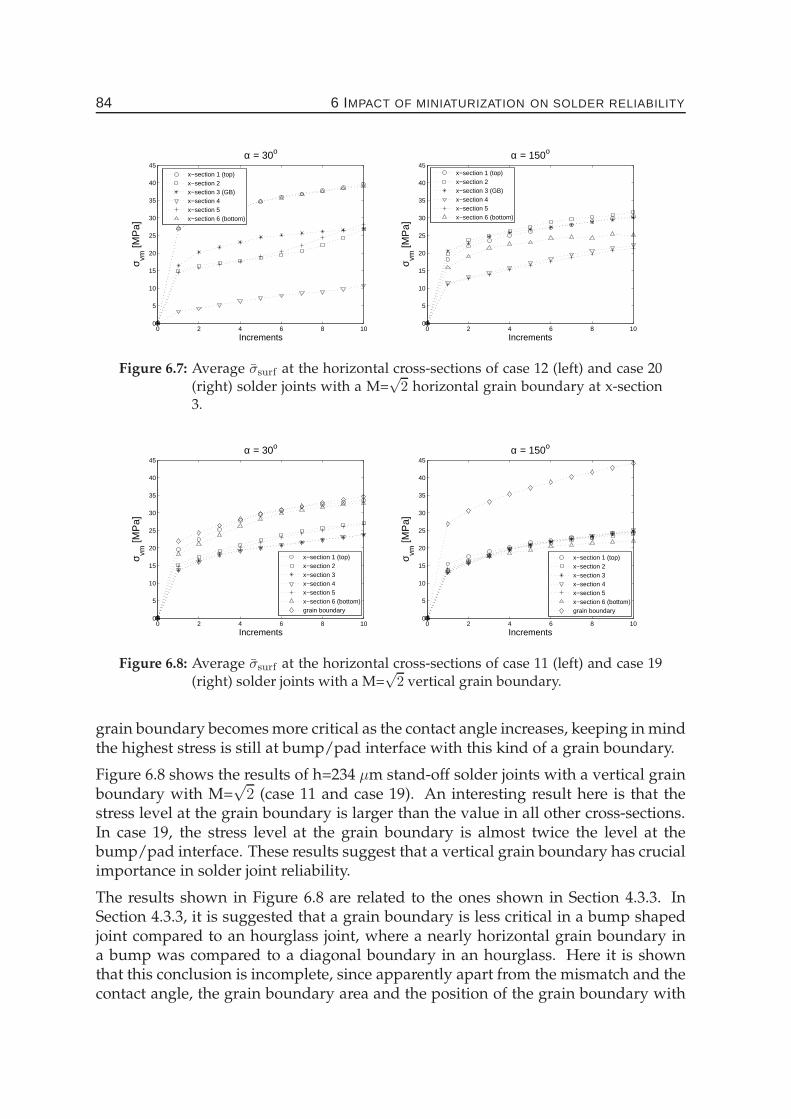
84 6 IMPACT OF MINIATURIZATION ON SOLDER RELIABILITY
0 2 4 6 8 100
5
10
15
20
25
30
35
40
45
Increments
σ vm [M
Pa]
α = 30ο
x−section 1 (top)x−section 2x−section 3 (GB)x−section 4x−section 5x−section 6 (bottom)
0 2 4 6 8 100
5
10
15
20
25
30
35
40
45
Increments
σ vm [M
Pa]
α = 150ο
x−section 1 (top)x−section 2x−section 3 (GB)x−section 4x−section 5x−section 6 (bottom)
Figure 6.7: Average σsurf at the horizontal cross-sections of case 12 (left) and case 20(right) solder joints with a M=
√2 horizontal grain boundary at x-section
3.
0 2 4 6 8 100
5
10
15
20
25
30
35
40
45
Increments
σ vm [M
Pa]
α = 30ο
x−section 1 (top)x−section 2x−section 3x−section 4x−section 5x−section 6 (bottom)grain boundary
0 2 4 6 8 100
5
10
15
20
25
30
35
40
45
Increments
σ vm [M
Pa]
α = 150ο
x−section 1 (top)x−section 2x−section 3x−section 4x−section 5x−section 6 (bottom)grain boundary
Figure 6.8: Average σsurf at the horizontal cross-sections of case 11 (left) and case 19(right) solder joints with a M=
√2 vertical grain boundary.
grain boundary becomes more critical as the contact angle increases, keeping in mindthe highest stress is still at bump/pad interface with this kind of a grain boundary.
Figure 6.8 shows the results of h=234 µm stand-off solder joints with a vertical grainboundary with M=
√2 (case 11 and case 19). An interesting result here is that the
stress level at the grain boundary is larger than the value in all other cross-sections.In case 19, the stress level at the grain boundary is almost twice the level at thebump/pad interface. These results suggest that a vertical grain boundary has crucialimportance in solder joint reliability.
The results shown in Figure 6.8 are related to the ones shown in Section 4.3.3. InSection 4.3.3, it is suggested that a grain boundary is less critical in a bump shapedjoint compared to an hourglass joint, where a nearly horizontal grain boundary ina bump was compared to a diagonal boundary in an hourglass. Here it is shownthat this conclusion is incomplete, since apparently apart from the mismatch and thecontact angle, the grain boundary area and the position of the grain boundary with

6.3 CONCLUSIONS 85
0.4 0.6 0.8 1 1.2 1.4 1.6 1.8 2 2.232
34
36
38
40
42
44
46
Microstructure factor
σ vm [M
Pa]
h=234µm, vert.
h=300µm, vert.
11 1315
17
19
21 2325
27
29
Figure 6.9: Microstructure factor vs. average σsurf on the grain boundaries, case num-bers are indicated.
respect to the pad planes are also factors that affect the stress concentration. For thisreason, the microstructure formulation given in Eqn. 6.3 is extended to include thegrain boundary position as follows:
MF′ =∑ Agb
d ∗ h∗ M ∗ sin β (6.4)
where β is the angle between the grain boundary normal and pad normal. In thisway, a horizontal grain boundary has no effect in the total microstructure factorwhereas a vertical grain boundary is fully taken into account.
In Figure 6.9, σsurf values for the grain boundaries are plotted in with respect to themicrostructure factor, calculated according to Eqn. 6.4. Horizontal grain boundariesare discarded since they are not critical. The stress level on grain boundaries clearlyincrease with increasing microstructure factor. Smaller stand-off pronounces this ef-fect. It can be concluded that vertical grain boundaries that touch the bump/padinterface have the highest average stress level under thermal loading and thus theyconstitute a possible crack initiation path.
6.3 Conclusions
With the ongoing miniaturization trend, it is a necessity to determine solder relia-bility with respect to size and to evaluate the increasing influence of microstructure.To this purpose, finite element slice models have been constructed for different con-tact angles and stand-off heights. The geometrical and microstructural criticality arequantified by describing a geometry factor and a microstructure factor. The geome-try factor is related to the solder shape, and the microstructure factor is related to thegrain boundary area and the mismatch of local crystallographic orientations at thegrain boundaries.
From the current study, the following conclusions are drawn:

86 6 IMPACT OF MINIATURIZATION ON SOLDER RELIABILITY
• As the geometry factor increases, cross-sectional averages of plastic strain andVon Mises stress values increase. Plastic strain is more sensitive to the geometryfactor than stress.
• A horizontal grain boundary becomes more critical as the contact angle in-creases. However the highest stress is still at bump/pad interface, thus a hori-zontal grain boundary is not critical compared to the overall.
• A vertical grain boundary may play a crucial role in solder joint reliability,which becomes more pronounced as the grain boundary area increases.
• The stress level at a grain boundary increases with increasing microstructurefactor. Smaller stand-off pronounces this effect.
• Vertical grain boundaries that touch the bump/pad interface have the high-est stress level under thermal loading and therefore constitute a possible crackinitiation path starting from the bump/pad interface.
Recommendations:In the finite element models discussed so far, substrate warpage, or bending, is notincluded. Warpage is negligible in small packages. In order to make a full stress anal-ysis for bigger packages, substrate bending has to be included as one of the boundaryconditions.
In this chapter, solder reliability analysis is conducted through plastic strain accu-mulation and equivalent Von Mises stresses. For a complete fatigue life analysis, thecohesive zone formulation for 3D shown in Chapter 5 should be employed as well.
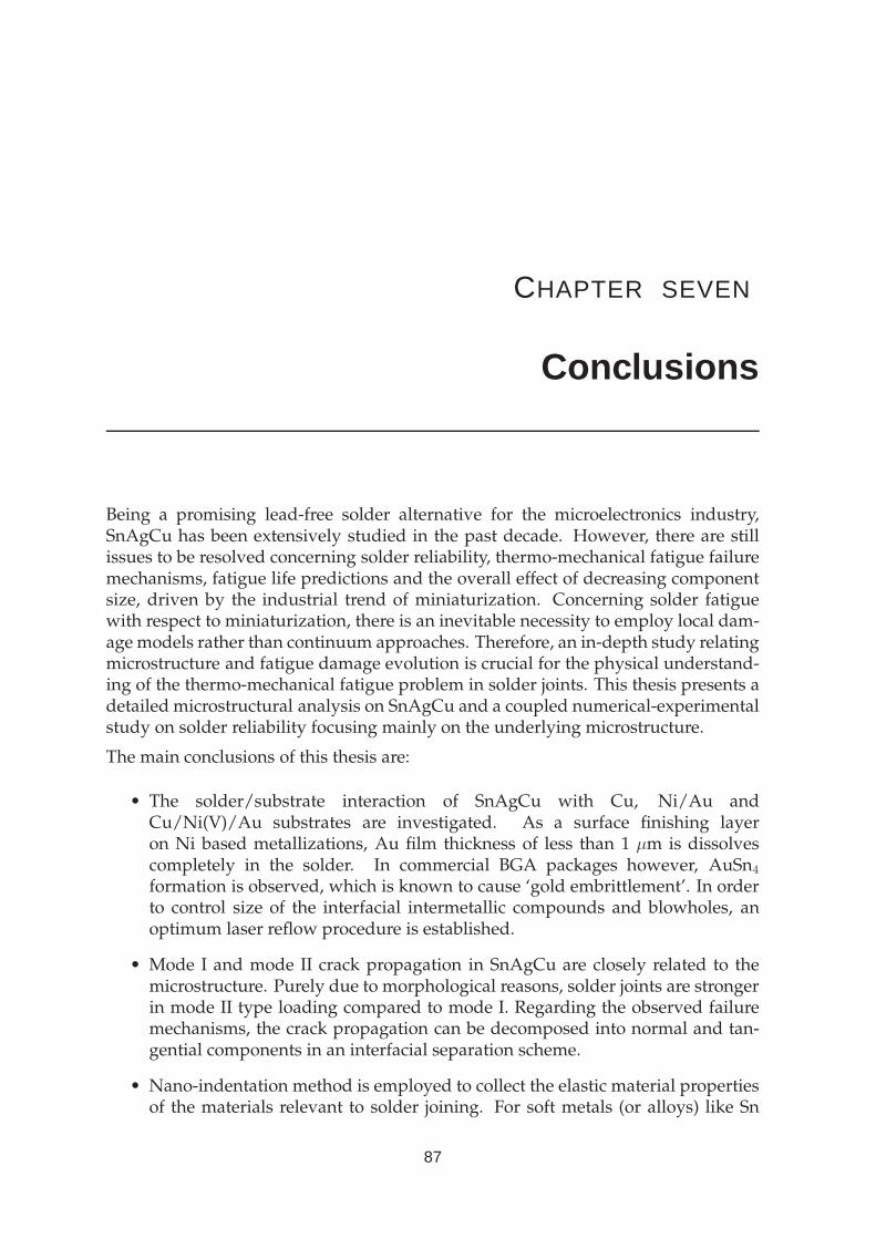
CHAPTER SEVEN
Conclusions
Being a promising lead-free solder alternative for the microelectronics industry,SnAgCu has been extensively studied in the past decade. However, there are stillissues to be resolved concerning solder reliability, thermo-mechanical fatigue failuremechanisms, fatigue life predictions and the overall effect of decreasing componentsize, driven by the industrial trend of miniaturization. Concerning solder fatiguewith respect to miniaturization, there is an inevitable necessity to employ local dam-age models rather than continuum approaches. Therefore, an in-depth study relatingmicrostructure and fatigue damage evolution is crucial for the physical understand-ing of the thermo-mechanical fatigue problem in solder joints. This thesis presents adetailed microstructural analysis on SnAgCu and a coupled numerical-experimentalstudy on solder reliability focusing mainly on the underlying microstructure.
The main conclusions of this thesis are:
• The solder/substrate interaction of SnAgCu with Cu, Ni/Au andCu/Ni(V)/Au substrates are investigated. As a surface finishing layeron Ni based metallizations, Au film thickness of less than 1 µm is dissolvescompletely in the solder. In commercial BGA packages however, AuSn4
formation is observed, which is known to cause ‘gold embrittlement’. In orderto control size of the interfacial intermetallic compounds and blowholes, anoptimum laser reflow procedure is established.
• Mode I and mode II crack propagation in SnAgCu are closely related to themicrostructure. Purely due to morphological reasons, solder joints are strongerin mode II type loading compared to mode I. Regarding the observed failuremechanisms, the crack propagation can be decomposed into normal and tan-gential components in an interfacial separation scheme.
• Nano-indentation method is employed to collect the elastic material propertiesof the materials relevant to solder joining. For soft metals (or alloys) like Sn
87
88 7 CONCLUSIONS
based solders, a strong influence of indentation parameters on the measuredmaterial properties is observed. Prolonging the peak hold time evokes time-dependent internal mechanisms. An assessment on indentation parameters forsolders is conducted.
• Depending on the joint size and geometry, two competitive damage mecha-nisms are identified under thermo-mechanical fatigue loading: bump/pad in-terfacial crack propagation and intergranular failure. Both mechanisms are ex-perimentally investigated and local damage models are developed by inversemodeling:
(i) In service use, the CTE mismatch between the package components leadsto cyclic thermo-mechanical strains in the solder joints. The ‘bump’ shapelocalizes these strains at the bump/pad interfaces, where the overall fail-ure is generally observed. Since the fatigue crack paths are known in ad-vance and the crack can be split into normal and tangential components,cohesive zones are used to simulate the fatigue crack propagation. A lineartraction-separation based cohesive zone model is proposed. An interfacialdamage variable is used to monitor the fatigue loading history. Using puretensile and pure shear fatigue tests, the damage evolution parameters forthe normal and the tangential openings in the cohesive zone model areidentified. An adequate agreement between experimental and numericalwork is established, whereby the cohesive zone approach is proven to bean effective tool in modeling solder joint fatigue failure.
(ii) In Sn based solders, the intrinsic thermal anisotropy of β-Sn causes causeslocal deformations especially on the grain boundaries under cyclic thermalloading. A size dependent cyclic softening behavior is observed. The me-chanical degradation of the specimens after temperature cycling is quan-tified from a reduction of the global elasticity modulus measured at smallstrains. Using OIM scans, the test specimens are simulated including thelocal grain orientations and the detailed microstructure. Using the devel-oped cohesive zone law, damage evolution parameters for thermal fatigueon Sn grain boundaries are identified on the basis of the mechanical re-sponse of the thermally cycled specimens. The representativeness of theparameters is investigated by a sensitivity analysis. It is shown that thedamage law characterized by experiments is capable of representing a va-riety of specimens which differ in grain size, orientation, and grain bound-ary geometry, provided that the specimen is still polycrystalline.
• Thermo-mechanical fatigue life of SnAgCu solder joints is size dependent.
• The amount of thermal fatigue damage on a Sn grain boundary is related toboth the local crystallographical mismatch and the grain boundary plane, givenby a ‘mismatch factor’. The mismatch factor in the literature is here extendedsuch that the crystallographically equivalent directions are also taken into ac-count.
89
• Thermo-mechanical damage localization in a solder ball is closely related to thejoint geometry and the amount of interfacial defects. A solder joint with a con-tact angle larger than 90◦ localizes strains at the joining interface, whereby theintegrity of the bump/pad interface is more important than the microstructurein this respect. For hourglass solder joints, where the contact angle is smallerthan 90◦, intergranular damage might dominate over interfacial damage de-pending on the crystallographical state.
• Manufacturing defects in EFSOT-BGA256 packages are optically examined.57% of all solder balls examined contained voids. 84% of all the voids observedwere on the chip side. Solder balls with big voids (>100 µm) were rare (<1%).If the solder contained a void, the voids volume appeared to be less than 1% ofthe solder ball volume in half of the cases.
• The numerical tools presented in 2D are extended to 3D for a complete de-scription of the industrial problem. Combining the data collected (i.e. materialproperties, microstructure, defects, local damage laws), 3D slice models repre-senting critical solder balls are constructed. The fatigue life of these models arepredicted and the results are validated by industrial failure distribution analy-ses of BGA packages. Using a critical damage value for the interfaces subjectedto fatigue damage, a good agreement with the experiments and simulationsis obtained. It is shown that microstructural modeling allows to predict andunderstand the scatter in the solder ball fatigue life observed in reality.
• The solder ball model developed so far is extended in order to predict the effectof miniaturization on interconnect reliability on the basis of numerical analy-ses. Finite element slice models are constructed separately for different contactangles with different stand-off heights. A geometry factor, related to the contactangle and the stand-off, and a microstructure factor, related to grain boundaryarea, grain boundary position and the mismatch of local crystallographic orien-tations at the grain boundaries are defined. The influence of these two factorson solder reliability is studied:
(i) As the geometry factor increases, both plastic strain and stress values in-crease. Plastic strain is affected more by the geometry factor than stress.
(ii) Vertical grain boundaries that touch the bump/pad interface have thehighest stresses under thermal loading and thus they create a possiblecrack path at the bump/pad interface. Horizontal grain boundaries donot affect the overall situation.

Bibliography
[1] Allen L.A., Notis M.R., Chromik R.R., and Vinci R.P. Microstructural evolutionin lead-free solder alloys: Part1, cast Sn-Ag-Cu eutectic. Journal of MaterialsResearch, 19:1417–1424, 2004.
[2] Matin M.A., Vellinga W.P., and Geers M.G.D. Quantitative microscopy of mi-crostructural evolution in eutectic solders subjected to static thermal load. InProceedings of EuroSimE, Aix-en-Provence, France, 2003.
[3] Abtew M. and Seldavuray G. Lead-free solders in microelectronics. MaterialsScience and Engineering R, 27:95–141, 2000.
[4] Luo W.C., Ho C.E., Tsai J.Y., Lin Y.L., and Kao C.R. Solid-state reactions betweenNi and SnAgCu solders with different Cu concentrations. Materials Science andEngineering A, 396:385–391, 2005.
[5] Kim K.S., Huh S.H., and Suganuma K. Effects of intermetallic compounds onproperties of SnAgCu lead-free soldered joints. Journal of Alloys and Compounds,352:226–236, 2003.
[6] Yoon J., Kim S., and Jung S. IMC morphology, interfacial reaction and jointreliability of Pb-free Sn-Ag-Cu solder on electrolytic Ni BGA substrate. Journalof Alloys and Compounds, 392:247–252, 2005.
[7] Chun H.S., Yoon J.W., and Jung S.B. Solid-state interfacial reactions betweenSn3.5Ag0.7Cu solder and electroless Ni-immersion Au substrate during hightemperature storage test. Journal of Alloys and Compounds, 439:91–96, 2007.
[8] Shih P.C. and Lin K.L. Spallation of interfacial AgAuCuZn compounds inSnAgCu/SnZnBi joints during 210oC reflow. Journal of Alloys and Compounds,439:137–142, 2007.
[9] Liu P.L. and J.K. Shang. Interfacial embrittlement by bismuth segregation incopper/tin-bismuth Pb-free solder interconnect. Metall. Mater. Trans. A, 31:286,2000.
91
92 BIBLIOGRAPHY
[10] Chan Y.C., Tu P.L., Tang C.W., K.C. Hung, and Lai K.L. Reliability studies of µ-BGA solder joints - effect of Ni-Sn intermetallic compound. Journal of MaterialsResearch, 24:25–32, 2001.
[11] Liu C.Y., Tu K.N., Sheng T.T., Tung C.H., Frear D.R., and Elenius P. Electron mi-croscopy study of interfacial reaction between eutectic SnPb and Cu/Ni(V)/Althin-film metallization. Journal of Applied Physics, 87:750–754, 2000.
[12] Zeng K. and Tu K.N. Six cases of reliability study of Pb-free solder joints inelectronic packaging technology. Materials Science and Engineering R, 38:55–105,2002.
[13] Li M., Zhang F., Chen W.T., Zeng K., Tu K.N., Balkan H., and EleniusP. Interfacial microstructure evolution between eutectic SnAgCu solder andAl/Ni(V)/Cu thin-films. Journal of Materials Research, 17:1612–1621, 2001.
[14] Ratchev P., Vandevelde B., and De Wolf I. Reliability and failure analysis ofSn-Ag-Cu solder interconnections for PSGA packages on Ni/Au surface finish.IEEE Transactions On Device And Materials Reliability, 4:5–10, 2004.
[15] Li D., Liu D., and Conway P.P. Characteristics of intermetallics and microme-chanical properties during thermal ageing of SnAgCu flip-chip solder intercon-nects. Materials Science and Engineering A, 391:95–103, 2005.
[16] Erinc M., Schreurs P.J.G., Zhang G.Q., and Geers M.G.D. Characterizationand fatigue damage simulation in SAC solder joints. Microelectronics Reliabil-ity, 44:1287–1292, 2004.
[17] Deng X., Chawla N., Chawla K.K., and Koopman M. Deformation behaviorof (Cu, Ag)Sn intermetallics by nanoindentation. Acta Materialia, 52:4291–4303,2004.
[18] Chromik R.R., Vinci R.P., Allen S.L., and Notis M.R. Nanoindentation measure-ments on Cu-Sn and Ag-Sn intermetallics formed in Pb-free solder joints. Journalof Materials Research, 18:2251, 2003.
[19] Rhee H., Lucas J.P., and Subramanian K.N. Micromechanical characterization ofthermomechanically fatigued lead-free solder joints. Journal of Materials Science:Materials in Electronics, 13:477–484, 2003.
[20] Liu H., Basaran C., Cartwright A.N., and Casey W. Application of moire in-terferometry to determine strain fields and debonding of solder joints in BGApackages. IEEE Transactions on Components and Packaging Technologies, 27:217–223, 2004.
[21] Stout E.A., Sottos N.R., and Skipor A.F. Mechanical characterization of plasticball grid array package flexure using moire interferometry. IEEE Transactions onAdvanced Packaging, 23:637–645, 2000.

BIBLIOGRAPHY 93
[22] Drexler S.E. Plastic strain in thermally cycled flip-chip PBGA solder bumps.IEEE Transactions on Advanced Packaging, 23:646–651, 2000.
[23] Oliver W.C. and Pharr G.M. An improved technique for determining hardnessand elastic modulus using load and displacement sensing indentation experi-ments. Journal of Materials Research, 7:1564, 1992.
[24] Matin M.A. Microstructure evolution and thermo-mechanical fatigue of solder mate-rials. PhD thesis, Technische Universiteit Eindhoven, 2005.
[25] Sharif A. and Chan Y.C. Interfacial reactions of Sn-3.5%Ag and Sn-3.5%Ag-0.5%Cu solder with electroless Ni/Au metallization during multiple reflow cy-cles. Journal of Materials Science: Materials in Electronics, 16:153–158, 2005.
[26] Erinc M., Schreurs P.J.G., Zhang G.Q., and M.G.D. Geers. Microstructural dam-age analysis of SnAgCu solder joints and an assessment on indentation proce-dures. Journal of Materials Science: Materials in Electronics, 16:93–100, 2005.
[27] Zeng K., Vuorinen V., and Kivilahti J.K. Interfacial reactions between lead-freeSnAgCu solder and Ni(P) surface finish on PWBs. IEEE Transactions on Electron-ics Packaging Manufacturing, 25:162–167, 2002.
[28] Plumbridge W.J., Gagg C.R., and Peters S. The creep of leadfree solders at ele-vated temperatures. Journal of Electronic Materials, 30:1178–1183, 2001.
[29] Wiese S., Feustel F., and Meusel E. Characterisation of constitutive behaviour ofSnAg, SnAgCu and SnPb solder in flip chip solder joints. Sensors and ActuatorsA, 99:188–193, 2002.
[30] Wiese S. and Wolter K.J. Microstructure and creep behaviour of eutectic SnAgand SnAgCu solders. Microelectronics Reliability, 44:1923–1931, 2004.
[31] Lin C.K. and Chu D.Y. Creep rupture of lead-free Sn-3.5Ag and Sn-3.5Ag-0.5Cusolders. Journal of Materials Science: Materials in Electronics, 16:355–365, 2005.
[32] Lee W.W., Nguyen L.T., and Selvaduray G.S. Solder joint fatigue models: reviewand applicability to chip scale packages. Microelectronics Reliability, 40:231–244,2000.
[33] Towashiraporn P., Subbarayan G., and Desai C.S. A hybrid model for com-putationally efficient fatigue fracture simulations at microelectronic assemblyinterfaces. International Journal of Solids and Structures, 42:4468–4483, 2005.
[34] GOM GmbH. Aramis v 5.3.0 User’s Manual, 2004.
[35] Metals Handbook, volume 8: Mechanical Testing, Fatigue Testing. Metals Park,Ohio: American Society for Metals, 9th edition, 1978-1989. pp:361–437.
[36] Visser J.W.W. Microstructure and deformation analysis of lead-free solder joints.Technical Report MT02.12, Technische Universiteit Eindhoven, 2002.
94 BIBLIOGRAPHY
[37] Dugdale D.S. Yielding in steel sheets containing slits. Journal of the Mechanicsand Physics of Solids, 8:100–104, 1960.
[38] Barenblatt G.I. The mathematical theory of equilibrium cracks in brittle fracture.Advances in Applied Mechanics, 7:55–129, 1962.
[39] Needleman A. An analysis of decohesion along an imperfect interface. Interna-tional Journal of Fracture, 42:21–40, 1990.
[40] Foulk J.W., Allen D.H., and Helms K.L.E. A model for predicting the damageand environmental degradation dependent life of SCS-6/Timetal21S[0]4 metalmatrix composite. Mechanics of Materials, 29:53–68, 1998.
[41] De-Andres A., Perez J.L., and Ortiz M. Elastoplastic finite element analysis ofthree-dimensional fatigue crack growth in aluminum shafts subjected to axialloading. International Journal of Solids and Structures, 36:2231–2258, 1999.
[42] Roe K.L. and Siegmund T. An irreversible cohesive zone model for interface fa-tigue crack growth simulation. Engineering Fracture Mechanics, 70:209–232, 2003.
[43] Abdul-Baqi A., Schreurs P.J.G., and Geers M.G.D. Fatigue damage modelingin solder interconnects using a cohesive zone approach. International Journal ofSolids and Structures, 42:927–942, 2005.
[44] Chaboche J.L., Feyel F., and Monerie Y. Interface debonding models: a viscousregularization with a limited rate dependency. International Journal of Solids andStructures, 38:3127–3160, 2001.
[45] Jang G.Y., Lee J.W., and Duh J.G. The nanoindentation characteristics of Cu6Sn5,Cu3Sn, and Ni3Sn4 intermetallic compounds in the solder bump. Jounal of Elec-tronics Materials, 33:1103–1110, 2004.
[46] Laurila T., Vuorinen V., and Kivilahti J.K. Interfacial reactions between lead-freesolders and common base materials. Materials Science and Engineering R, 49:1–60,2005.
[47] Matin A., Coenen E.W.C., Vellinga W.P., and Geers M.G.D. Correlation betweenthermal fatigue and thermal anisotropy in a Pb-free solder alloy. Scripta Materi-alia, 53:927–932, 2006.
[48] Subramanian K.N. and Lee J.G. Effect of anisotropy of tin on thermomechanicalbehavior of solder joints. Journal of Materials Science: Materials in Electronics,15:235–240, 2004.
[49] Telang A.U., Bieler T.R., Lucas J.P., Subramanian K.N., Lehman L.P., Xing Y.,and Cotts E.J. Grain-boundary character and grain growth in bulk tin and bulklead-free solder alloys. Journal of Electronic Materials, 33:1412–1423, 2004.

BIBLIOGRAPHY 95
[50] Vianco P.T., Rejent J.A., and Kilgo A.C. Creep behavior of the ternary 95.5Sn-3.9Ag-0.6Cu solder: Part ii–aged condition. Journal of Electronic Materials,33:1473–1484, 2004.
[51] Erinc M., Schreurs P.J.G., and M.G.D. Zhang. A coupled numerical and exper-imental study on thermo-mechanical fatigue failure in SnAgCu solder joints.Proceedings in EuroSimE, London, 2007.
[52] De Vries J.W.C., Jansen M.Y., and Van Driel W.D. The effect of board stiffnesson the solder-joint reliability of HVQFN-packages. In Proceedings of EuroSimE,London, England, 2007.
[53] Telang A.U., Bieler T.R., and Crimp M.A. Grain boundary sliding on near-7◦,14◦, and 22◦ special boundaries during thermomechanical cycling in surface-mount lead-free solder joint specimens. Materials Science and Engineering A,421:22–34, 2006.
[54] Pearson W.B. A handbook of lattice spacings and structure of metals and alloys, vol-ume 2. Pergamon Press, London, 1958.
[55] Lea C. A Scientific Guide to Surface Mount Technology. Electrochemical Publica-tions Ltd., GB-Port Erin, British Isles, 1988.
[56] Lewis W.R. Notes on Soldering. Tin Research Institute, 1961.
[57] Matin M.A., Vellinga W. P., and Geers M.G.D. Aspects of coarsening in eutecticSnPb. Acta Materialia, 52:3475–3482, 2004.
[58] Ubachs R.L.J.M., Schreurs P.J.G., and Geers M.G.D. Elasto-viscoplastic nonlocaldamage modelling of thermal fatigue in anisotropic lead-free solder. Mechanicsof Materials, 39:685–701, 2007.
[59] Liu X., Xu S., Lu G.Q., and Dillard D.A. Stacked solder bumping technology forimproved solder joint reliability. Microelectronics Reliability, 41:1979–1992, 2001.
[60] Lee H.T., Lin H.S., Lee C.S., and Chen P.W. Reliability of Sn-Ag-Sb lead-freesolder joints. Materials Science and Engineering A, 407:36–44, 2005.
[61] Erinc M., Schreurs P.J.G., and Geers M.G.D. Integrated numerical-experimentalanalysis of interfacial fatigue fracture in SnAgCu solder joints. International Jour-nal of Solids and Structures, 44:5680–5694, 2007.
[62] Erinc M., Schreurs P.J.G., and Geers M.G.D. Intergranular thermal fatigue dam-age evolution in snagcu lead-free solder joints. Mechanics of Materials, submitted,2007b.
[63] Tchankov D., Sakane M., Itoh T., and Hamada N. Crack opening displacementapproach to assess multiaxial low cycle fatigue. International Journal of Fatigue,in press, 2007.
96 BIBLIOGRAPHY
[64] Desai C.S., Basaran C., Dishong T., and Prince J.L. Thermomechanical analysisin electronic packaging with unified constitutive model for materials and joints.IEEE Transactions on Components, Packaging, and Manufacturing Technology – PartB, 21:87–97, 1998.
[65] Li X. and Wang Z. Thermo-fatigue life evaluation of SnAgCu solder joints inflip chip assemblies. Journal of Materials Processing Technology, 18:6–12, 2007.
[66] Tee T.Y., Ng H.S., Yap D., Baraton X., and Zhong Z. Board level solder jointreliability modeling and testing of TFBGA packages for telecommunication ap-plications. Microelectronics Reliabilty, 43:1117–1123, 2003.
[67] Zhang X., Kripesh V., Chai T.C., Tan T.C., and Pinjala D. Board level solderjoint reliability analysis of a fine pitch Cu post type wafer level package (WLP).Microelectronics Reliability, in press, 2007.
[68] Lai Y.S., Wang T.H., and Lee C.C. Thermal-mechanical coupling analysis forcoupled power and thermal cycling reliability of chip-scale packages. In Pro-ceedings of EuroSimE, Berlin, Germany, 2005.
[69] De Vries J.W.C., Jansen M.Y., and Van Driel W.D. On the difference betweenthermal cycling and thermal shock testing for board level reliability of solderedinterconnections. Journal of Microelectronics & Reliability, 47:444–449, 2007.
[70] Yeung B.H. and Lee T.T.T. Evaluation and optimization of package processing,design, and reliability through solder joint profile prediction. In Proceedings of51st ECTC, 2001.
[71] National Institute of Standards and Technology.www.metallurgy.nist.gov/solder/clech/Sn-Ag-Cu Fit.htm, 2007.
[72] Towashiraporn P., Subbarayan G., McIlvanie B., Hunter B.C., Love D., and Sul-livan B. The effect of model building on the accuracy of fatigue life predictionsin electronic packages. Microelectronics Reliability, 44:115–127, 2004.
[73] Armin R. The Basics of Soldering. John Wiley & Sons, 1993.
[74] Frear D.R. The mechanical behavior of interconnect materials for electronicpackaging. Journal of Metals, 48:49–53, 1996.
[75] Guo F., Choi S., Subramanian K.N., Bieler T.R., Lucas J.P., Achari A., andParuchuri M. Evaluation of creep behavior of near-eutectic Sn-Ag solders con-taining small amount of alloy additions. Materials Science and Engineering A,351:190–199, 2003.
[76] Kariya Y., Morihata T., Hazawa E., and Otsuka M. Assessment of low-cyclefatigue life of Sn-3.5mass%Ag-X(X=Bi or Cu)alloy by strain range partitioningapproach. Journal of Electronic Materials, 30:1184–1189, 2001.
BIBLIOGRAPHY 97
[77] Kempf B., Graff M., Hutin O., and Rettenmayr M. Lead-free Ball-Grid-Arrayballs: Production method and properties. Journal of Electronic Materials, 31:1270–1275, 2002.
[78] Kim H.K., Tu K.N., and Totta P.A. Ripening-assisted asymmetric spalling ofCu-Sn compound spheroids in solder joints on Si wafers. Applied Physics Letters,68:2204, 1996.
[79] Lee H.T., Chen M.H., Jao H.M., and Liao T.L. Influence of interfacial intermetal-lic compound on fracture behavior of solder joints. Materials Science and Engi-neering A, 358:134–141, 2003.
[80] Liu X. Processing and Reliability Assessment of Solder Joint Interconnection for PowerChips. PhD thesis, Virginia Polytechnic Institute and State University, 2001.
[81] Liu A.A., Kim H.K., and Tu K.N. Spalling of Cu6Sn5 spheroids in the solderingreaction of eutectic SnPb on Cr/Cu/Au thin films. Journal of Applied Physics,80:2774, 1996.
[82] Poon N.M., Wu C.M.L., Lai J.K.L., and Chan Y.C. Residual shear strength ofSn-Ag and Sn-Bi lead-free SMT joints after thermal shock. IEEE Transactions onAdvanced Packaging, 23:708–714, 2000.
[83] Spraul M., Nuchter W., Moller A., Wunderle B., and Michel B. Reliability ofSnPb and Pb-free flip chips under different test conditions. Microelectronics Reli-ability, 47:252–258, 2007.
[84] Stam F.A. and Davitt E. Effects of thermomechanical cycling on lead and lead-free (SnPb and SnAgCu) surface mount solder joints. Microelectronics Reliability,41:1815–1822, 2001.
[85] Suganuma K. and Nakamura Y. Microstructure and strength of interface be-tween Sn-Ag eutectic solder and Cu. Journal of Japanese Institute of Metals,59:1299–1305, 1995.
[86] Van den Bosch M.J., Schreurs P.J.G., and Geers M.G.D. An improved descrip-tion of the exponential Xu and Needleman cohesive zone law for mixed-modedecohesion. Engineering Fracture Mechanics, 73:1220–1234, 2006.
[87] Vandevelde B., Gonzalez M., Limaye P., Ratchev P., and Beyne E. Thermal cy-cling reliability of SnAgCu and SnPb solder joints: A comparison for severalIC-packages. Microelectronics Reliability, 47:259–265, 2007.
[88] Yu D.Q., Zhao J., and Wang L. Improvement on the microstructure stability, me-chanical and wetting properties of Sn-Ag-Cu lead-free solder with the additionof rare earth elements. Journal of Alloys and Compounds, 376:170–175, 2004.

98 BIBLIOGRAPHY
Samenvatting
Volgens de EU-norm, opgesteld door de Electrical and Electronic Equipment Direc-tive (WEEE) en de Restriction of Hazardous Substances Directive (RoHS), is het ge-bruik van lood in electronische apparaten niet meer toegestaan vanaf 1 juli 2006. Insoldeerverbindingen wordt de PbSn-soldeer daarom vervangen door een SnAgCu-legering, die een stabiele microstructuur heeft met goede kruip- en vermoeiingsei-genschappen. Hoewel er de afgelopen tien jaar veel onderzoek is gedaan naar de ei-genschappen van SnAgCu, bestaan er nog steeds onduidelijkheden ten aanzien vande te verwachten levensduur van de soldeerverbindingen, waarin ze worden toege-past, vooral in samenhang met de steeds verdergaande miniaturisatie. In dit proef-schrift wordt beschreven hoe via een gekoppelde experimenteel-numerieke werkwij-ze, de mechanismen bij thermo-mechanisch bezwijken zijn onderzocht.
In de micro-electronica bestaat de soldeerverbinding bij zogenaamde Ball Grid Ar-rays (BGA’s) uit een soldeer bump tussen verbindingsplaatsen (pads) op chip en Prin-ted Circuit Board (PCB). De betrouwbaarheid van de soldeerverbinding wordt voor-al bepaald door de metallisatie van en de defecten in het overgangsgebied (interfa-ce) tussen bump en pad. Om dit te onderzoeken zijn oldeerbumps, soldeerpasta engegoten eutectisch SnAgCu aangebracht op een Cu, Ni/Au en Cu/Ni(V)/Au me-tallisatie. De invloed van dit substraat op de metallurgie van soldeer en interface isonderzocht, evenals de voortplanting van defecten in SnAgCu-soldeerverbindingenop Cu en Ni/Au metallisatie. Het belangrijkste bezwijkmechanisme bleek localisatievan schade in de bump/pad interface, zodat geconcludeerd kon worden dat een con-tinuumsmodel niet geschikt is voor bestudering van het fenomeen. De mechanischeeigenschappen van SnAgCu zijn gekarakteriseerd met nano-indentatie experimen-ten en trekproeven. De invloed van de Ag concentratie op deze eigenschappen isonderzocht.
Een van de belangrijkste oorzaken van het bezwijken van BGA’s, namelijk scheur-voortplanting tijdens wisselende thermo-mechanische belasting, wordt vrijwel altijdwaargenomen in de bump/pad interface. Dit thermo-mechanisch vermoeiingsge-drag van SnAgCu/Ni-Au verbindingen is daarom nader onderzocht. Allereerst zijnvermoeiingsexperimenten uitgevoerd om de evolutie van defecten in de bump/padinterface te karakteriseren. Schade bleek op te treden zowel in het soldeermateriaal
99

100 SAMENVATTING
van de bump als in de bump/pad interface. Bezwijken van de interface trad meestalop bij grote initiele spanningen en bij geringe soldeer volumes. Scheurvoortplan-ting werd vervolgens gesimuleerd met een cohesive zone model, waarbij de interactiekracht tussen twee punten aan beide zijden van de interface lineair gerelateerd wordtaan hun relatieve verplaatsing (=opening van de interface). De stijfheid in normaleen tangentiele richting wordt door wisselende belasting gereduceerd m.b.v. een scha-deparameter, waarvan de toename – van 0 (geen schade) tot 1 (volledig bezwijken) –beschreven wordt door een schade-evolutievergelijking. De schadegroeiparametersin deze relatie zijn bepaald door fitten van experimentele en numerieke resultaten.
Bij wisselende temperatuurbelasting ontstaat schade in de bump/pad interface t.g.v.het verschil in thermische uitzettingscoefficient van de diverse materialen. In hetsoldeermateriaal zelf veroorzaakt de anisotropie in thermische eigenschappen vande Sn β-fase lokale deformaties in de kristalgrenzen, die resulteren in thermischevermoeiingsschade. Om dit nader te onderzoeken zijn SnAgCu-proefstukken her-haald verwarmd tot 125o C en afgekoeld tot -40o C. Daarna werden ze onderworpenaan mechanische belasting om via metingen van de stijfheid de vermoeiingsscha-de te karakteriseren. Het verband tussen kracht en verlenging tijdens een trekproefliet verzwakkend materiaalgedrag (softening) zien, dat afhankelijk bleek te zijn vande proefstuk geometrie (scale effect). Van alle proefstukken is een numeriek eindigeelementenmodel gemaakt, inclusief kristallen met kristallografische orientaties vaneigenschappen. Ook zijn cohesive zone elementen aangebracht tussen de kristal-len. De microstructuur was vooraf gemeten m.b.v. Orientation Imaging Microscopy(OIM). Zowel de wisselende temperatuurbelasting als de erop volgende trekproefzijn met het model gesimuleerd. Door fitten van experimentele en numerieke re-sultaten, konden de schadegroeiparameters van de interkristallijne cohesive zonesworden bepaald. Een twee-dimensionaal model van de hele soldeerverbinding metdaarin kristallen, kristalgrenzen, bump/pad en interkristallijne cohesive zones, isvervolgens gebruikt om vermoeiingslevensduur te voorspellen. Gebleken is dat hetbezwijkgedrag afhangt van de geometrie.
Ten behoeve van een realistische analyse is een drie-dimensionaal slice-model vaneen soldeerverbinding gemaakt, bestaande uit een soldeerbump en een aangrenzenddeel van chip en PCB. Ook nu is de microstructuur gemodelleerd inclusief cohesivezones in bump/pad interface en tussen kristallen. De microstructuur is gebaseerdop OIM-data van diverse SnAgCu-soldeerbumps. Modellering van defecten zoalsblow holes is gebaseerd op statistisch onderzoek van BGA’s, resulterend in gegevensover grootte, positie en aantal. Diverse modellen zijn geanalyseerd, waarna de datastatistisch zijn verwerkt. Vermoeiingslevensduur wordt door de modellen voorspelden vergeleken met gegevens uit de industriele praktijk. De invloed van de grootte,vorm en microstructuur van de soldeerbump op het bezwijkgedrag van de soldeer-verbinding, is onderzocht.

Acknowledgements
With deep gratitude I would first like to thank my promoter Marc Geers, for makingthis thesis possible by his faith in me to manage a numerical-experimental study con-sidering my materials science background. His positive and constructive personalitycombined with deep knowledge made this task an educative and a truly enjoyableone. Second, I would like to thank my copromotor Piet Schreurs. I have benefitedfrom his everyday availability, the friendly attitude and pragmatic approach to thenumerical problems. In short, Marc and Piet, it was a very pleasant and satisfactorytime of my life, hartelijk bedankt!
I sincerely thank the committee members; prof.dr.ir. Bert Verlinden, prof.dr.ir. JaapM.J. den Toonder, prof.dr.ir. Jeff Th.M. De Hosson, dr.ing. Steffen Wiese andprof.dr.ir. Kouchi Zhang for their valuable comments on this thesis. Special thanksto Kouchi Zhang for his supervision in 2003-2004.
I would like to thank my fellow project members, Rene Ubachs and Abdul Matin. Itwas nice to see how our work completed each other, which resulted in one numerical,one experimental and a coupled numerical-experimental work. Thanks for all thediscussions and the scientific input, and all the nice time we had together duringconferences! Next, I sincerely thank the STW members who had the time to join ourmeetings and contributed to this work by the fruitful discussions.
Marcel Kouters, Peter Teesink and Tim Assman contributed this thesis during theirbachelor end projects, their work is much appreciated. Very special thanks to Hansde Vries from Philips App.Tech., for that he always had time for me and was alwayswilling to help me. I would also like to acknowledge Willem van Driel from NXPSemiconductors for the nice discussions we had and the ‘custom made specimens’ inNijmegen, in 2003-2004.
Marc van Maris, thanks for running all the machinary, teaching us how to use them,and for the good ideas in constructing challenging set-ups. Sjef, thank you very muchfor machining n (n>500) samples for me. Patrick & Leo, thanks for all the hardware& software you have arranged, and also for your patience in n (n>3) times changingmy tea-spilled-keyboard. Alice, Yvon and Marleen, thanks for your kindness, andfor not following the ‘minimum answer principle’ that governs this country.
I would like to thank my friends and colleagues, basically all MATE people; An-
101

102 ACKNOWLEDGEMENTS
ish, Arash, Bhairav, Erica, Frederico, Gabriel, Jan, Jesus, Johan, Katja, Hamid, Hans,Linda, Marcel, Marco, Matej, Michiel, MK, Mohammad, Murthy, Peter, Roel, Ron,Sebastiaan and Varya. Here, a special subset has to be mentioned, the Turkish cluster,Barıs, Cem, Kanat, Isa, Izzet, Ozlem and Tuncay. The lunches we had together weretruly, homely.
Then, I would like to thank for all the quality time I had with Quadrivium, especiallyVokollage, and The Knights (KotKT). I am very grateful to my friends in Eindhoven,Bianca, Jessica and Nele for their warm company, and to the old friends in mete-abroad for the e-support to every single one of us wherever we are in the world.
My special thanks goes to all Van Meijltjes and Rullenraadjes, especially Andre en Le-nie. There are no words to express my gratitude to my mum and dad, and my familyin Ankara, who have unconditionally loved and supported me all these years. Fi-nally, many thanks to my husband, William, for that I have the most enjoyable -evenfruitful- nurdiest discussions with you, and in the mean time share such uncondi-tional love and care. If you were a melody, it would only be the good notes.
Muge ErincEindhoven, December 2007.
Curriculum Vitae
2.10.1978 Born in Ankara, Turkey.
1984–1995 Primary, secondary and high school in TED Ankara College, Ankara, Turkey.
1995–2000 Bachelor’s Degree, Metallurgical & Materials Engineering Department, MiddleEast Technical University, Ankara, Turkey.
2001–2003 Master’s Degree, Metallurgical & Materials Engineering Department, under su-pervision of Prof.Dr. E. Tekin, Research topic: ‘Isothermal Transformations inLow Alloy Steels at Sub-Ms temperatures’, Middle East Technical University,Ankara, Turkey.
2003–2007 PhD, Mechanical Engineering Department, Institute of Materials Technology,under supervision of prof.dr.ir. M.G.D. Geers, Research topic: ‘Thermomechan-ical fatigue failure of interfaces in lead-free solders’, Eindhoven University ofTechnology, The Netherlands.
103


![Article A Novel Method for High Temperature Fatigue Testing of … · 2021. 3. 16. · et al. [22] developed a complex thermomechanical fatigue (TMF) test rig with loading, heating,](https://img.dokumen.tips/doc/110x75/6148eeaa9241b00fbd673b82/article-a-novel-method-for-high-temperature-fatigue-testing-of-2021-3-16-et.jpg)


![Effect of Constitutive Model on Thermomechanical Fatigue ... · subjected automotive powertrain components to severe thermomechanical fatigue (TMF) loadings [1]. The design against](https://img.dokumen.tips/doc/110x75/5e932c9e8a6031207607f5b6/effect-of-constitutive-model-on-thermomechanical-fatigue-subjected-automotive.jpg)


