Embed Size (px)
Citation preview
PPGCC
Pontifícia Universidade Católica do RioGrande do Sul
Faculdade de InformáticaPós-Graduação em Ciência da Computação
Non-Volatile Memory: Emerging Technologies And
Their Impacts on Memory Systems
Taciano Perez, César A. F. De Rose
Technical Report Nº 060
Porto Alegre, September 2010
Abstract
For almost 30 years, computer memory systems have been essentially the same: volatile,high speed memory technologies like SRAM and DRAM used for cache and main memory;magnetic disks for high-end data storage; and persistent, low speed �ash memory for storagewith low capacity/low energy consumption requirements such as embedded/mobile devices.Today we watch the emergence of new non-volatile memory technologies, such as Phase-Change RAM (PCRAM), Magnetoresistive RAM (MRAM) and Resistive RAM (RRAM),that promise to radically change the landscape of memory systems. This paper summarizesthe current state of memory system design, presents these new memory technologies andsurveys the current proposals on how to apply these technologies to improve memoryhierarchies. We conclude that the introduction of these new technologies will probablyresult in more complex memory hierarchies, but is likely to allow the construction ofmemory chips that are non-volatile, low-energy and have density and latency close to orbetter than current DRAM chips, improving performance/e�ciency and allowing memorysystems to continue to scale up.
2
Contents
ABSTRACT 2
Chapter 1: Introduction 5
Chapter 2: Memory Systems: Current Landscape 62.1 Processor Cache: SRAM . . . . . . . . . . . . . . . . . . . . . . . . . . . . 72.2 Main Memory: DRAM . . . . . . . . . . . . . . . . . . . . . . . . . . . . . 92.3 Persistent Storage: Disk, Flash . . . . . . . . . . . . . . . . . . . . . . . . 112.4 Limitations of Current Memory Technologies . . . . . . . . . . . . . . . . . 13
2.4.1 A Note on Energy-Proportional Computing . . . . . . . . . . . . . 15
Chapter 3: Emerging Memory Technologies 173.1 Phase-Change RAM (PCRAM) . . . . . . . . . . . . . . . . . . . . . . . . 173.2 Resistive RAM (RRAM) . . . . . . . . . . . . . . . . . . . . . . . . . . . . 18
3.2.1 Memristor . . . . . . . . . . . . . . . . . . . . . . . . . . . . . . . . 193.3 Magnetoresistive RAM (MRAM) . . . . . . . . . . . . . . . . . . . . . . . 21
3.3.1 STT-RAM . . . . . . . . . . . . . . . . . . . . . . . . . . . . . . . . 223.4 Comparison Between Memory Technologies . . . . . . . . . . . . . . . . . . 23
Chapter 4: Impacts on Memory Systems 254.1 Cache . . . . . . . . . . . . . . . . . . . . . . . . . . . . . . . . . . . . . . 25
4.1.1 MRAM as L2 and L3 cache . . . . . . . . . . . . . . . . . . . . . . 254.1.2 Hybrid SRAM/MRAM and SRAM/PCRAM as L2 and L3 caches . 264.1.3 Fault-tolerant architecture for NVM caches . . . . . . . . . . . . . . 27
4.2 Main Memory . . . . . . . . . . . . . . . . . . . . . . . . . . . . . . . . . . 274.2.1 Pioneer work: �ash-based main memory . . . . . . . . . . . . . . . 274.2.2 PCRAM as main memory . . . . . . . . . . . . . . . . . . . . . . . 28
4.2.2.1 Improving latency, energy and endurance through bu�erorganization and partial writes . . . . . . . . . . . . . . . 28
3
4.2.2.2 Improving endurance and energy consumption through 3Dstacking . . . . . . . . . . . . . . . . . . . . . . . . . . . . 29
4.2.2.3 Combining both approaches . . . . . . . . . . . . . . . . . 304.2.3 Hybrid PCRAM-DRAM main memory . . . . . . . . . . . . . . . . 30
4.2.3.1 Qureshi et al. hybrid approach . . . . . . . . . . . . . . . 304.2.3.2 FLAM hybrid approach . . . . . . . . . . . . . . . . . . . 314.2.3.3 BPRAM hybrid approach . . . . . . . . . . . . . . . . . . 32
4.3 Persistent Storage . . . . . . . . . . . . . . . . . . . . . . . . . . . . . . . . 334.3.1 PCRAM as a disk replacement . . . . . . . . . . . . . . . . . . . . 334.3.2 PCRAM or STT-MRAM as disk replacement . . . . . . . . . . . . 34
4.4 Other Memory Systems . . . . . . . . . . . . . . . . . . . . . . . . . . . . . 364.4.1 PCRAM for MPP checkpointing . . . . . . . . . . . . . . . . . . . . 364.4.2 MRAM in GPU. . . . . . . . . . . . . . . . . . . . . . . . . . . . . 37
4.5 Operating System . . . . . . . . . . . . . . . . . . . . . . . . . . . . . . . . 374.5.1 OS improvements to support FLAM. . . . . . . . . . . . . . . . . . 374.5.2 BPFS �le system . . . . . . . . . . . . . . . . . . . . . . . . . . . . 38
Chapter 5: Conclusion 40
BIBLIOGRAPHY 42
4
1 Introduction
For almost 30 years the memory hierarchy used in computer design has been essentiallythe same: volatile, high speed memory technologies like SRAM and DRAM used for cacheand main memory; magnetic disks for high-end data storage; and persistent, low speed�ash memory for storage with low capacity/low energy consumption requirements, such asembedded/mobile devices [13].
Today we watch the emergence of new memory technologies under research that promiseto change signi�cantly the landscape of memory systems. Non-Volatile Memory (NVM)technologies such as Phase-Change RAM (PCRAM), Magnetic RAM (MRAM) and Re-sistive RAM (RRAM) will possibly enable memory chips that are non-volatile, requirelow-energy and have density and latency closer to current DRAM chips [4].
Even though most of these technologies are still in early prototyping stages, their ex-pected properties in terms of density, latency, energy and endurance are already estimated.Based on these estimations, several papers have been published proposing practical appli-cations for these new NVM technologies. These papers provide initial insight on what theimpacts on memory systems should be if such technologies evolve to be competitive in themarket.
The memory system is one of the most critical components of modern computers. It hasattained a high level of complexity due to the many layers involved in memory hierarchy:application software, operating system, cache, main memory and disk. Any relevant changein one level of the memory hierarchy (such as the introduction of the aforementioned NVMtechnologies) can potentially impact several other layers and overall system behavior. Forthis reason, it is essential to consider the di�erent possible scenarios for using these newmemory technologies from a broad perspective.
There are several studies that explore the impact of new NVM technologies on speci�cparts of the memory system, but we are not aware of any comprehensive survey of theliterature on potential applications of new NVM technologies. The intention of the presentwork is to provide such comprehensive survey. To attain this goal, it is divided in foursections:
1. A review of the current technologies used in memory systems.
2. A presentation of the most relevant NVM technologies currently under research:PCRAM, RRAM and MRAM.
3. A survey of the practical applications proposed so far for these technologies.
4. A discussion of their implications for memory system design.
5
2 Memory Systems: Current Landscape
In order to discuss the emergent NVM technologies, we need to start by summarizing thecurrent state of memory systems. This is a well-known subject, and we have extractedmost of the information present in this section from the comprehensive textbook Memory
Systems: Cache, DRAM, Disk by Bruce Jacob, Spencer W. Ng and David T. Wang [13]and Ulrich Drepper's online paper What Every Programmer Should Know About Memory
[9].An ideal memory system would be fast, cheap, persistent and big (highly dense). Until
now, all known memory/storage technologies address only some of these characteristics.Static RAM (SRAM) is very fast, but it's expensive, has low density and is not persistent.Dynamic RAM (DRAM) has better densities and is cheaper (but still expensive) at thecost of being a little slower, and it's not persistent as well. Disks are cheap, highly denseand persistent, but very slow. Flash memory is between DRAM and disk; it is a persistentsolid-state memory with higher densities than DRAM, but its write latency is much higherthan the latter.
Fortunately, it is possible to design a memory system that incorporates all these di�er-ent technologies in a single memory hierarchy. Such hierarchy allows the creation of asystem that approaches the performance of the fastest component, the cost of the cheapestcomponent and energy consumption of the most power-e�cient component. This is pos-sible due to a phenomenon known as locality of reference, so named because memoryreferences tend to be localized in time and space. This can be so summarized:
� If you use something once, you are likely to use it again (temporal locality).
� If you use something once, you are likely to use its neighbor (spatial locality) [13].
This phenomenon can be exploited by creating di�erent memory levels; the �rst levels aresmaller and more expensive, but have fastest access, and the other layers are progressivelybigger and cheaper, but have slower access times. Appropriate heuristics are then appliedto decide which data will be accessed more often and place them at the �rst levels, andmove the data down on the hierarchy as it ceases to be used frequently. Figure 2.1 depictsthe concept of memory hierarchy.
For at least the last 30 years, we have been building memory hierarchies that rely onSRAM for caches, DRAM for main memory and disk or �ash as persistent storage. In thenext sections we will describe these technologies in more detail.
6
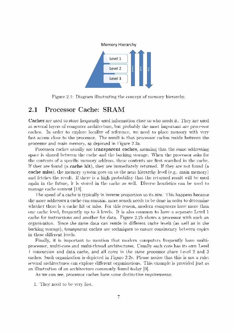
Figure 2.1: Diagram illustrating the concept of memory hierarchy.
2.1 Processor Cache: SRAM
Caches are used to store frequently used information close to who needs it. They are usedat several layers of computer architecture, but probably the most important are processorcaches. In order to explore locality of reference, we need to place memory with veryfast access close to the processor. The result is that processor caches reside between theprocessor and main memory, as depicted in Figure 2.2a.
Processor caches usually are transparent caches, meaning that the same addressingspace is shared between the cache and the backing storage. When the processor asks forthe contents of a speci�c memory address, these contents are �rst searched in the cache.If they are found (a cache hit), they are immediately returned. If they are not found (acache miss), the memory system goes on to the next hierarchy level (e.g., main memory)and fetches the result. If there is a high probability that the returned result will be usedagain in the future, it is stored in the cache as well. Diverse heuristics can be used tomanage cache content [13].
The speed of a cache is typically in inverse proportion to its size. This happens becausethe more addresses a cache can contain, more search needs to be done in order to determinewhether there is a cache hit or miss. For this reason, modern computers have more thanone cache level, frequently up to 3 levels. It is also common to have a separate Level 1cache for instructions and another for data. Figure 2.2b shows a processor with such anorganization. Since the same data can reside in di�erent cache levels (as well as in thebacking storage), transparent caches use techniques to ensure consistency between copiesin these di�erent levels.
Finally, it is important to mention that modern computers frequently have multi-processor, multi-core and multi-thread architectures. Usually each core has its own Level1 instruction and data cache, and all cores in the same processor share Level 2 and 3caches. Such organization is depicted in Figure 2.2c. Please notice that this is not a rule:several architectures can explore di�erent organizations. This example is provided just asan illustration of an architecture commonly found today [9].
As we can see, processor caches have some distinctive requirements:
1. They need to be very fast.
7
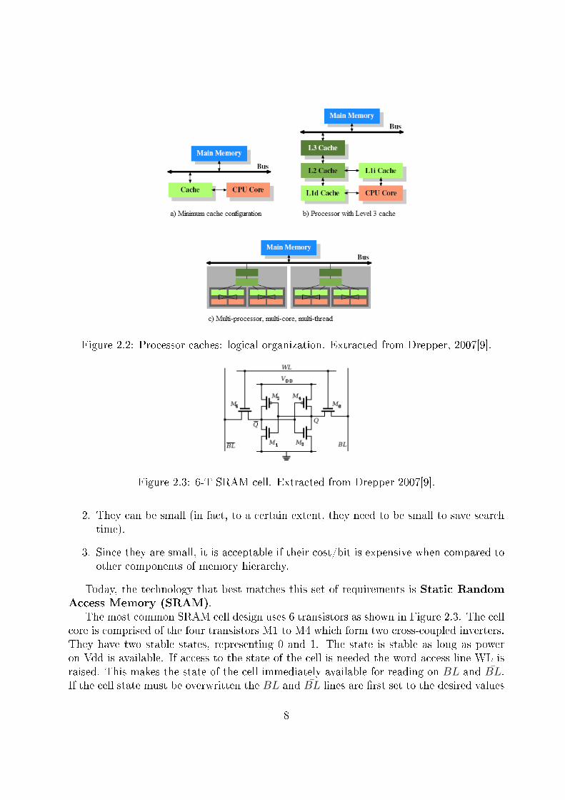
Figure 2.2: Processor caches: logical organization. Extracted from Drepper, 2007[9].
Figure 2.3: 6-T SRAM cell. Extracted from Drepper 2007[9].
2. They can be small (in fact, to a certain extent, they need to be small to save searchtime).
3. Since they are small, it is acceptable if their cost/bit is expensive when compared toother components of memory hierarchy.
Today, the technology that best matches this set of requirements is Static RandomAccess Memory (SRAM).
The most common SRAM cell design uses 6 transistors as shown in Figure 2.3. The cellcore is comprised of the four transistors M1 to M4 which form two cross-coupled inverters.They have two stable states, representing 0 and 1. The state is stable as long as poweron Vdd is available. If access to the state of the cell is needed the word access line WL israised. This makes the state of the cell immediately available for reading on BL and B̄L.If the cell state must be overwritten the BL and B̄L lines are �rst set to the desired values
8
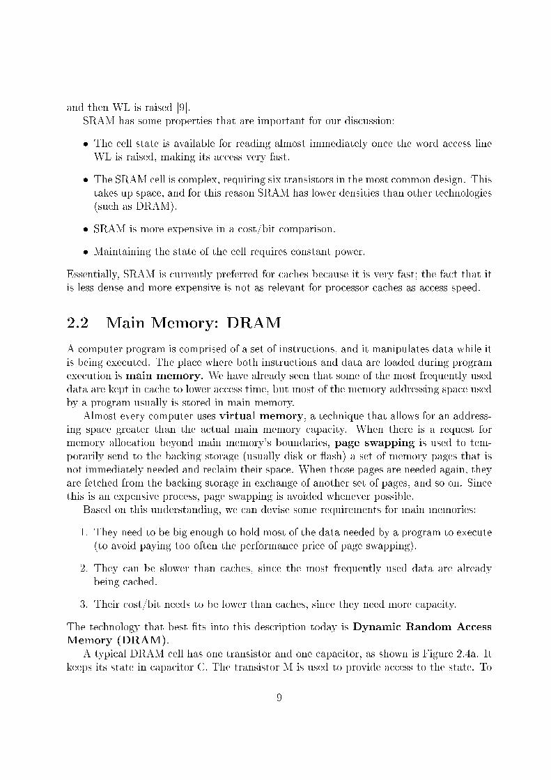
and then WL is raised [9].SRAM has some properties that are important for our discussion:
� The cell state is available for reading almost immediately once the word access lineWL is raised, making its access very fast.
� The SRAM cell is complex, requiring six transistors in the most common design. Thistakes up space, and for this reason SRAM has lower densities than other technologies(such as DRAM).
� SRAM is more expensive in a cost/bit comparison.
� Maintaining the state of the cell requires constant power.
Essentially, SRAM is currently preferred for caches because it is very fast; the fact that itis less dense and more expensive is not as relevant for processor caches as access speed.
2.2 Main Memory: DRAM
A computer program is comprised of a set of instructions, and it manipulates data while itis being executed. The place where both instructions and data are loaded during programexecution is main memory. We have already seen that some of the most frequently useddata are kept in cache to lower access time, but most of the memory addressing space usedby a program usually is stored in main memory.
Almost every computer uses virtual memory, a technique that allows for an address-ing space greater than the actual main memory capacity. When there is a request formemory allocation beyond main memory's boundaries, page swapping is used to tem-porarily send to the backing storage (usually disk or �ash) a set of memory pages that isnot immediately needed and reclaim their space. When those pages are needed again, theyare fetched from the backing storage in exchange of another set of pages, and so on. Sincethis is an expensive process, page swapping is avoided whenever possible.
Based on this understanding, we can devise some requirements for main memories:
1. They need to be big enough to hold most of the data needed by a program to execute(to avoid paying too often the performance price of page swapping).
2. They can be slower than caches, since the most frequently used data are alreadybeing cached.
3. Their cost/bit needs to be lower than caches, since they need more capacity.
The technology that best �ts into this description today is Dynamic Random AccessMemory (DRAM).
A typical DRAM cell has one transistor and one capacitor, as shown is Figure 2.4a. Itkeeps its state in capacitor C. The transistor M is used to provide access to the state. To
9
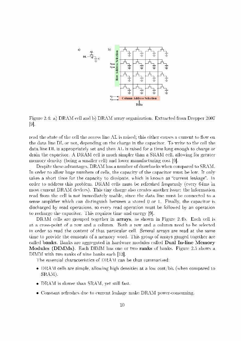
Figure 2.4: a) DRAM cell and b) DRAM array organization. Extracted from Drepper 2007[9].
read the state of the cell the access line AL is raised; this either causes a current to �ow onthe data line DL or not, depending on the charge in the capacitor. To write to the cell thedata line DL is appropriately set and then AL is raised for a time long enough to charge ordrain the capacitor. A DRAM cell is much simpler than a SRAM cell, allowing for greatermemory density (being a smaller cell) and lower manufacturing cost [9].
Despite these advantages, DRAM has a number of drawbacks when compared to SRAM.In order to allow huge numbers of cells, the capacity of the capacitor must be low. It onlytakes a short time for the capacity to dissipate, which is known as �current leakage�. Inorder to address this problem, DRAM cells must be refreshed frequently (every 64ms inmost current DRAM devices). This tiny charge also creates another issue: the informationread from the cell is not immediately usable, since the data line must be connected to asense ampli�er which can distinguish between a stored 0 or 1. Finally, the capacitor isdischarged by read operations, so every read operation must be followed by an operationto recharge the capacitor. This requires time and energy [9].
DRAM cells are grouped together in arrays, as shown in Figure 2.4b. Each cell isat a cross-point of a row and a column. Both a row and a column need to be selectedin order to read the content of that particular cell. Several arrays are read at the sametime to provide the contents of a memory word. This group of arrays ganged together arecalled banks. Banks are aggregated in hardware modules called Dual In-line MemoryModules (DIMMs). Each DIMM has one or two ranks of banks. Figure 2.5 shows aDIMM with two ranks of nine banks each [13].
The essential characteristics of DRAM can be thus summarized:
� DRAM cells are simple, allowing high densities at a low cost/bit (when compared toSRAM).
� DRAM is slower than SRAM, yet still fast.
� Constant refreshes due to current leakage make DRAM power-consuming.
10
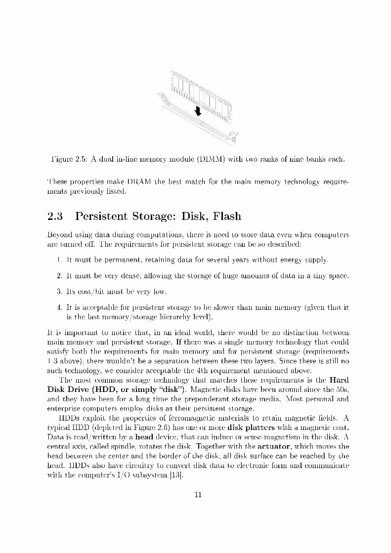
Figure 2.5: A dual in-line memory module (DIMM) with two ranks of nine banks each.
These properties make DRAM the best match for the main memory technology require-ments previously listed.
2.3 Persistent Storage: Disk, Flash
Beyond using data during computations, there is need to store data even when computersare turned o�. The requirements for persistent storage can be so described:
1. It must be permanent, retaining data for several years without energy supply.
2. It must be very dense, allowing the storage of huge amounts of data in a tiny space.
3. Its cost/bit must be very low.
4. It is acceptable for persistent storage to be slower than main memory (given that itis the last memory/storage hierarchy level).
It is important to notice that, in an ideal world, there would be no distinction betweenmain memory and persistent storage. If there was a single memory technology that couldsatisfy both the requirements for main memory and for persistent storage (requirements1-3 above), there wouldn't be a separation between these two layers. Since there is still nosuch technology, we consider acceptable the 4th requirement mentioned above.
The most common storage technology that matches these requirements is the HardDisk Drive (HDD, or simply �disk�). Magnetic disks have been around since the 50s,and they have been for a long time the preponderant storage media. Most personal andenterprise computers employ disks as their persistent storage.
HDDs exploit the properties of ferromagnetic materials to retain magnetic �elds. Atypical HDD (depicted in Figure 2.6) has one or more disk platters with a magnetic coat.Data is read/written by a head device, that can induce or sense magnetism in the disk. Acentral axis, called spindle, rotates the disk. Together with the actuator, which moves thehead between the center and the border of the disk, all disk surface can be reached by thehead. HDDs also have circuitry to convert disk data to electronic form and communicatewith the computer's I/O subsystem [13].
11
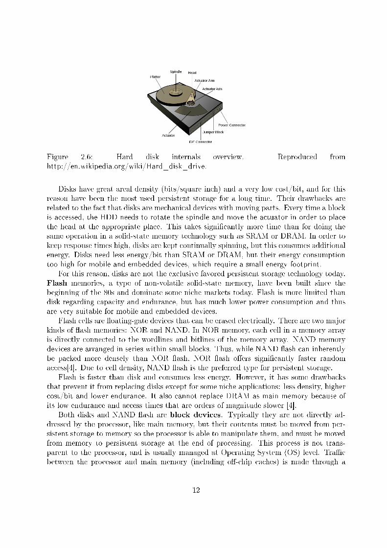
Figure 2.6: Hard disk internals overview. Reproduced fromhttp://en.wikipedia.org/wiki/Hard_disk_drive.
Disks have great areal density (bits/square inch) and a very low cost/bit, and for thisreason have been the most used persistent storage for a long time. Their drawbacks arerelated to the fact that disks are mechanical devices with moving parts. Every time a blockis accessed, the HDD needs to rotate the spindle and move the actuator in order to placethe head at the appropriate place. This takes signi�cantly more time than for doing thesame operation in a solid-state memory technology such as SRAM or DRAM. In order tokeep response times high, disks are kept continually spinning, but this consumes additionalenergy. Disks need less energy/bit than SRAM or DRAM, but their energy consumptiontoo high for mobile and embedded devices, which require a small energy footprint.
For this reason, disks are not the exclusive favored persistent storage technology today.Flash memories, a type of non-volatile solid-state memory, have been built since thebeginning of the 80s and dominate some niche markets today. Flash is more limited thandisk regarding capacity and endurance, but has much lower power consumption and thusare very suitable for mobile and embedded devices.
Flash cells are �oating-gate devices that can be erased electrically. There are two majorkinds of �ash memories: NOR and NAND. In NOR memory, each cell in a memory arrayis directly connected to the wordlines and bitlines of the memory array. NAND memorydevices are arranged in series within small blocks. Thus, while NAND �ash can inherentlybe packed more densely than NOR �ash, NOR �ash o�ers signi�cantly faster randomaccess[4]. Due to cell density, NAND �ash is the preferred type for persistent storage.
Flash is faster than disk and consumes less energy. However, it has some drawbacksthat prevent it from replacing disks except for some niche applications: less density, highercost/bit and lower endurance. It also cannot replace DRAM as main memory because ofits low endurance and access times that are orders of magnitude slower [4].
Both disks and NAND �ash are block devices. Typically they are not directly ad-dressed by the processor, like main memory, but their contents must be moved from per-sistent storage to memory so the processor is able to manipulate them, and must be movedfrom memory to persistent storage at the end of processing. This process is not trans-parent to the processor, and is usually managed at Operating System (OS) level. Tra�cbetween the processor and main memory (including o�-chip caches) is made through a
12
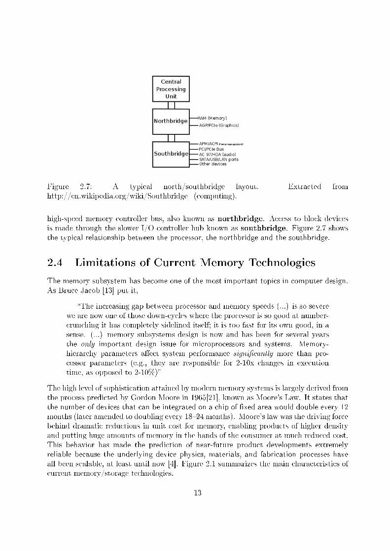
Figure 2.7: A typical north/southbridge layout. Extracted fromhttp://en.wikipedia.org/wiki/Southbridge_(computing).
high-speed memory controller bus, also known as northbridge. Access to block devicesis made through the slower I/O controller hub known as southbridge. Figure 2.7 showsthe typical relationship between the processor, the northbridge and the southbridge.
2.4 Limitations of Current Memory Technologies
The memory subsystem has become one of the most important topics in computer design.As Bruce Jacob [13] put it,
�The increasing gap between processor and memory speeds (...) is so severewe are now one of those down-cycles where the processor is so good at number-crunching it has completely sidelined itself; it is too fast for its own good, in asense. (...) memory subsystems design is now and has been for several yearsthe only important design issue for microprocessors and systems. Memory-hierarchy parameters a�ect system performance signi�cantly more than pro-cessor parameters (e.g., they are responsible for 2-10x changes in executiontime, as opposed to 2-10%)�
The high level of sophistication attained by modern memory systems is largely derived fromthe process predicted by Gordon Moore in 1965[21], known as Moore's Law. It states thatthe number of devices that can be integrated on a chip of �xed area would double every 12months (later amended to doubling every 18�24 months). Moore's law was the driving forcebehind dramatic reductions in unit cost for memory, enabling products of higher densityand putting huge amounts of memory in the hands of the consumer at much reduced cost.This behavior has made the prediction of near-future product developments extremelyreliable because the underlying device physics, materials, and fabrication processes haveall been scalable, at least until now [4]. Figure 2.1 summarizes the main characteristics ofcurrent memory/storage technologies.
13
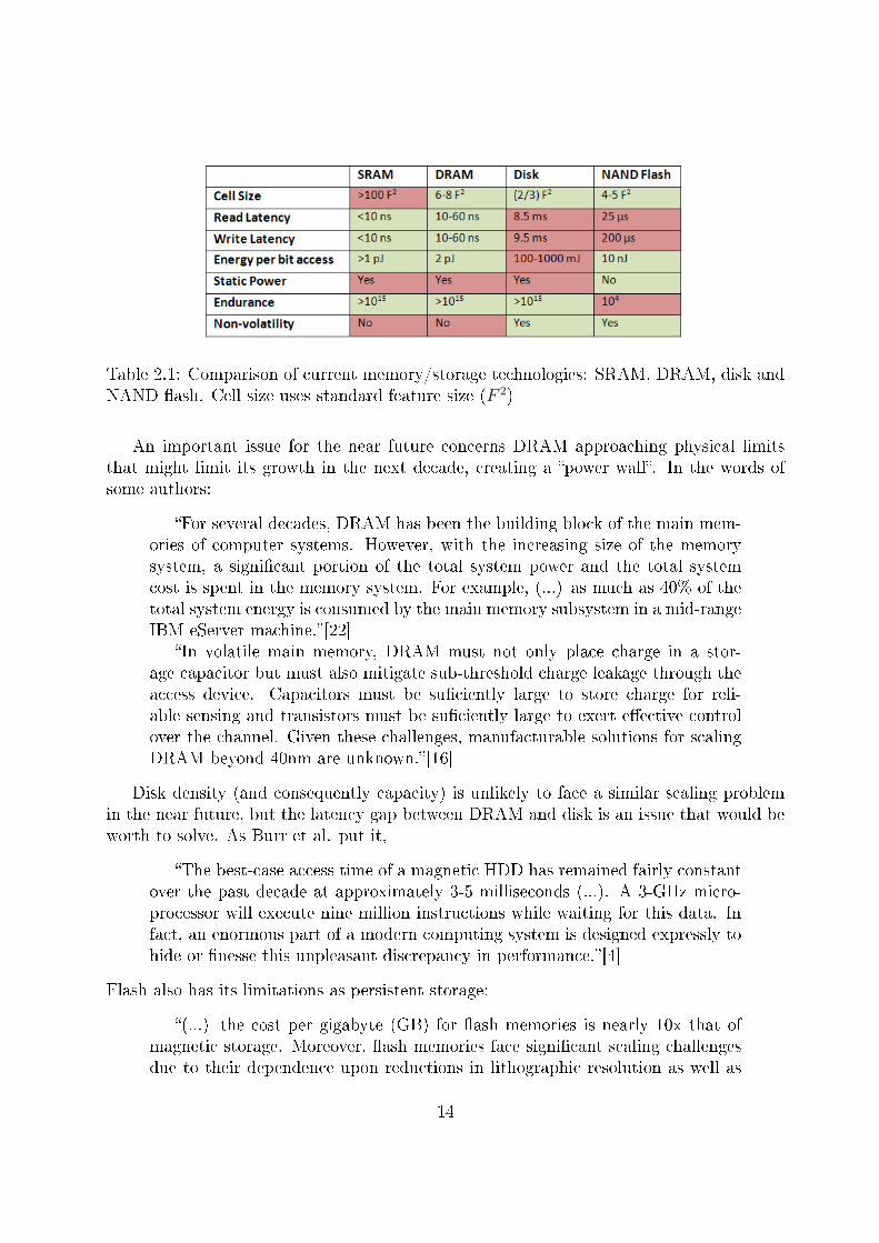
Table 2.1: Comparison of current memory/storage technologies: SRAM, DRAM, disk andNAND �ash. Cell size uses standard feature size (F 2)
An important issue for the near future concerns DRAM approaching physical limitsthat might limit its growth in the next decade, creating a �power wall�. In the words ofsome authors:
�For several decades, DRAM has been the building block of the main mem-ories of computer systems. However, with the increasing size of the memorysystem, a signi�cant portion of the total system power and the total systemcost is spent in the memory system. For example, (...) as much as 40% of thetotal system energy is consumed by the main memory subsystem in a mid-rangeIBM eServer machine.�[22]
�In volatile main memory, DRAM must not only place charge in a stor-age capacitor but must also mitigate sub-threshold charge leakage through theaccess device. Capacitors must be su�ciently large to store charge for reli-able sensing and transistors must be su�ciently large to exert e�ective controlover the channel. Given these challenges, manufacturable solutions for scalingDRAM beyond 40nm are unknown.�[16]
Disk density (and consequently capacity) is unlikely to face a similar scaling problemin the near future, but the latency gap between DRAM and disk is an issue that would beworth to solve. As Burr et al. put it,
�The best-case access time of a magnetic HDD has remained fairly constantover the past decade at approximately 3-5 milliseconds (...). A 3-GHz micro-processor will execute nine million instructions while waiting for this data. Infact, an enormous part of a modern computing system is designed expressly tohide or �nesse this unpleasant discrepancy in performance.�[4]
Flash also has its limitations as persistent storage:
�(...) the cost per gigabyte (GB) for �ash memories is nearly 10x that ofmagnetic storage. Moreover, �ash memories face signi�cant scaling challengesdue to their dependence upon reductions in lithographic resolution as well as
14
fundamental physical limitations beyond the 22 nm process node, such as severe�oating gate interference, lower coupling ratio, short channel e�ects, and lowelectron charge in the �oating gate. Thus, to replace HDDs, alternative NVMtechnologies that can overcome the shortcomings of NAND �ash memories andcompete on a cost per TB basis with HDDs must be found.�[15]
...and as main memory:
�NAND �ash has very limited number of write/erase cycles: 105 rewritesas opposed to 1016 for DRAM. NAND �ash also requires a block to be erasedbefore writing into that block, which introduces considerably extra delay andenergy. Moreover, NAND �ash is not byte-addressable.�[31]
Due to these limitations, there is intense research to create new alternatives of memorytechnology that can address these problems and prevent a �power wall� from being reached.In the next chapter we will present some of the most promising technologies under research.
2.4.1 A Note on Energy-Proportional Computing
Many of the technologies that will be presented in the next chapter can signi�cantly lowerthe power requirements of caches, main memory and persistent storage. We would like topoint out that not only the power requirements are lower, but that the energy consumptionbehavior of such systems is di�erent, exhibiting energy proportionality, a behavior thatcan be specially bene�cial for datacenter environments.
In a 2007 article, Barroso and Hölzle [2] proposed the notion of energy-proportionalcomputing and maintained that it should be a primary design goal for computer design.They argue that datacenters are designed to keep server workload between 10-50% oftheir maximum utilization levels. This is done to ensure that throughput and latencyservice-level agreements will be met and that there will be room for handling componentfailures and planned maintenance. The problem is that the region under 50% utilization isthe lowest energy-e�cient region of servers, due to static power consumption (depicted inFigure 2.8a). As seen, memory/storage components consume both dynamic power (usedto change memory contents) and static power (used for data retention and componentavailability). Static power used by SRAM and DRAM is used mostly for refreshes dueto power leakage; in disks, most static power is used to keep the disk spinning and readyto answer requests with low latencies. As Barroso and Hölzle put it, �essentially, even anenergy-e�cient server still consumes about half of its full power when doing virtually nowork�[2]. This problem is aggravated by the fact that the costs are not re�ected only inthe server electricity bill, but also in energy for cooling the datacenter and infrastructureprovisioning costs, that increase proportionally to the server energy budget.
The authors of the article also mention that CPUs are the components that exhibitmost energy-proportional behavior today, and that the components that most contributeto less server energy e�ciency are, in this order, DRAM (50%), disk drives (25%) andnetworking switches (15%). A machine with a dynamic power range of 90% could cut by
15
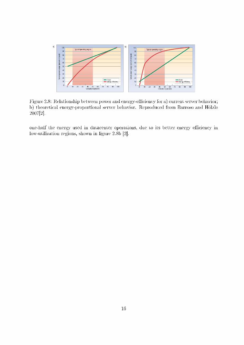
Figure 2.8: Relationship between power and energy-e�ciency for a) current server behavior;b) theoretical energy-proportional server behavior. Reproduced from Barroso and Hölzle2007[2].
one-half the energy used in datacenter operations, due to its better energy e�ciency inlow-utilization regions, shown in �gure 2.8b [2].
16
3 Emerging Memory Technologies
There are several new Non-Volatile Memory (NVM) technologies under research. Onestudy lists 13 such technologies: FRAM, MRAM, STTRAM, PCRAM, NRAM, RRAM,CBRAM, SEM, Polymer, Molecular, Racetrack, Holographic and Probe [15]. Most thesetechnologies are in di�erent stages of maturity. Some of them are still in early researchstages, others have working prototypes, and some of them are already entering into com-mercial manufacturing.
In the present work, we will limit our study to three of these technologies: Phase-ChangeRAM, Resistive RAM (including Memristors) and Magnetoresistive RAM (including Spin-Torque Transfer RAM). All these fall into the category of the most actively researchedtoday, are backed by solid companies of the technology industry, and considered mostpromising of being commercially feasible.
For readers interested in a more broad analysis of all di�erent kinds of NVM underresearch, the works of Burr et al. [4], and Kryder and Kim [15]can be consulted.
3.1 Phase-Change RAM (PCRAM)
Phase-Change Random Access Memory (also called PCRAM, PRAM or PCM) is currentlythe most mature of the new memory technologies under research. It relies on some ma-terials, called phase-change materials, that exist in two di�erent phases with distinctproperties:
1. An amorphous phase, characterized by high electrical resistivity;
2. A crystalline phase, characterized by low electrical resistivity [10].
These two phases can be repeatedly and rapidly cycled by applying heat to the material. Tomake it amorphous, it is melt-quenched using a high-power electrical pulse that is abruptlycut o�. To crystallize the material, it is heated above its crystallization temperature usinga moderate power pulse with a longer duration. Since the duration of this pulse variesaccording to the crystallization speed of the material being used, this operation tends todictate the writing speed of PCRAM. Re�ectivity can vary up to 30%, but resistivitychanges can be as large as �ve orders of magnitude [10, 4].
The principle of phase-change memory is known since the 1960s, but only recent dis-coveries of phase-change materials with faster crystallization speeds led to the possibility ofcommercially feasible memory technology. The most important materials are chalcogenidessuch as Ge2Sb2Te5 (GST), that can crystallize in less than 100 ns [10].
17
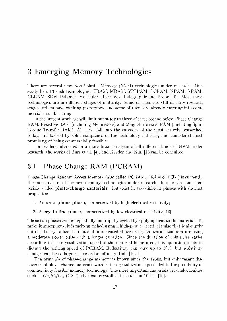
Figure 3.1: Example of a phase-change memory cell. The current is forced to pass throughthe phase-change material. Image obtained from [10].
Figure 3.1 shows a memory cell based on phase-change principles. The SET operationis achieved by crystallizing the material and RESET by making it amorphous. UnlikeFlash memory, PCRAM can be switched from 0 to 1 and vice-versa without an ERASEoperation.
Given the great di�erence in resistance, phase-change materials can be easily used tostore binary states per cell (single-level cell) and even more states (multi-level cell) [4, 16].
PCRAM is argued to be a scalable technology. As the feature density increases, phase-change material layers become thinner and need less current for the programming oper-ations. It has been demonstrated to work in 20nm device prototype and is projected toscale down to 9nm. DRAM probably will not able to scale down beyond 40nm [10, 16].
As previously mentioned, the SET latency is the longest and determines the writeperformance. Latencies of 150 ns for SET and 40 ns for RESET operations have beendemonstrated. Write energy is determined by the RESET operation, which dissipates 480µW , while SET dissipates 90 µW . The read latency is 48 ns and dissipates 40 µW . Bothread and write latencies are several times slower than DRAM, although only by tens ofnanoseconds [16].
Endurance is bound to the number of writes. This happens because when currentis injected into a phase-change material, thermal expansion and contraction degrade thecontacts, so that currents are no more reliably injected into the cell. The current writeendurance varies between 104 and 109 writes, but we can conservatively assume 108 as areasonable reference value [16, 31].
Today PCRAM is positioned as a Flash replacement. It o�ers great advantages overFlash, but given the current limitations of access latency, energy consumption and en-durance, further development is required in order to employ it as a replacement for DRAM[16, 17].
3.2 Resistive RAM (RRAM)
Despite the fact that PCRAM also uses resistance variations to store bit values, the termResistive RAM (RRAM or ReRAM) has been applied to a distinct set of technologies
18
that explore the same phenomenon. Essentially these technologies fall into one of twocategories [4]:
1. Insulator resistive memories: based on bipolar resistance switching properties of somemetal oxides. The most important example is the memristor memory device, whichwill be further described in more detail.
2. Solid-electrolyte memories: based on solid-electrolyte containing mobile metal ionssandwiched between a cathode and an anode. Also known as Programmable Metal-lization Cell (PMC) or Conductive Bridge RAM (CBRAM).
There is a long list of RRAM technologies [3, 4, 15, 30]. In this paper we will concentrateour attention on thememristor, which is currently the most promising RRAM technologyunder research [30].
3.2.1 Memristor
Since the 19th century, three fundamental passive circuit elements were known: the resistor,the inductor and the capacitor. In 1971, Leon Chua theorized the existence of a fourthpassive circuit element, which he called the memristor [5], but no actual physical devicewith memristive properties could be constructed. In 2008, a group of scientists reportedthe invention of a device that behaved as predicted for a memristor[24]. Later the sameyear, an article detailed how that device could be used to create nonvolatile memories [30].
The property of memristors particularly relevant to memory devices is the nonlinearrelationship between current (I) and voltage (V), depicted on Figure 3.2. In the wordsof R. Stanley Williams, the leader of the research team that invented the �rst memristordevice:
�Memristor is a contraction of 'memory resistor', because that is exactlyits function: to remember its history. A memristor is a two-terminal devicewhose resistance depends on the magnitude and polarity of the voltage appliedto it and the length of time that voltage has been applied. When you turn o�the voltage, the memristor remembers its most recent resistance until the nexttime you turn it on, whether that happens a day later or a year later. (...) Theability to inde�nitely store resistance values means that a memristor can beused as a nonvolatile memory.�[26]
This memristor device consisted of a crossbar of platinum wires with titanium dioxide(TiO2) switches, as shown in Figure 3.3. Each switch consists of a lower layer of perfecttitanium dioxide (TiO2), which is electrically insulating, and an upper layer of oxygen-de�cient titanium dioxide (TiO2−x), which is conductive. The size of each layer can bechanged by applying voltage to the top electrode. If a positive voltage is applied, theTiO2−xlayer thickness increases and the switch becomes conductive (ON state). A negativevoltage has the opposite e�ect (OFF state). This behavior matches the hysteresis looppreviously shown in Figure 3.2 [24, 30, 26].
19
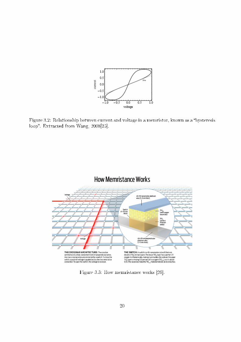
Figure 3.2: Relationship between current and voltage in a memristor, known as a �hysteresisloop�. Extracted from Wang, 2008[25].
Figure 3.3: How memristance works [26].
20
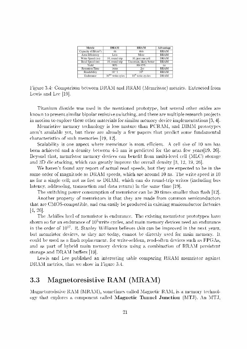
Figure 3.4: Comparison between DRAM and RRAM (Memristor) metrics. Extracted fromLewis and Lee [19].
Titanium dioxide was used in the mentioned prototype, but several other oxides areknown to present similar bipolar resistive switching, and there are multiple research projectsin motion to explore these other materials for similar memory device implementations [3, 4].
Memristive memory technology is less mature than PCRAM, and DIMM prototypesaren't available yet, but there are already a few papers that predict some fundamentalcharacteristics of such memories [19, 12].
Scalability is one aspect where memristor is most e�cient. A cell size of 10 nm hasbeen achieved and a density between 4-5 nm is predicted for the next few years[19, 26].Beyond that, memristor memory devices can bene�t from multi-level cell (MLC) storageand 3D die stacking, which can greatly improve the overall density [3, 12, 19, 26].
We haven't found any report of actual read speeds, but they are expected to be in thesame order of magnitude as DRAM speeds, which are around 10 ns. The write speed is 10ns for a single cell; not as fast as DRAM, which can do round-trip writes (including buslatency, addressing, transaction and data return) in the same time [19].
The switching power consumption of memristor can be 20 times smaller than �ash [12].Another property of memristors is that they are made from common semiconductors
that are CMOS-compatible, and can easily be produced in existing semiconductor factories[4, 26].
The Achilles heel of memristor is endurance. The existing memristor prototypes haveshown so far an endurance of 105write cycles, and main memory devices need an endurancein the order of 1017. R. Stanley Williams believes this can be improved in the next years,but memristor devices, as they are today, cannot be directly used for main memory. Itcould be used as a �ash replacement, for write-seldom, read-often devices such as FPGAs,and as part of hybrid main memory devices using a combination of RRAM persistentstorage and DRAM bu�ers [19].
Lewis and Lee published an interesting table comparing RRAM memristor againstDRAM metrics, that we show in Figure 3.4.
3.3 Magnetoresistive RAM (MRAM)
Magnetoresistive RAM (MRAM), sometimes called Magnetic RAM, is a memory technol-ogy that explores a component called Magnetic Tunnel Junction (MTJ). An MTJ,
21
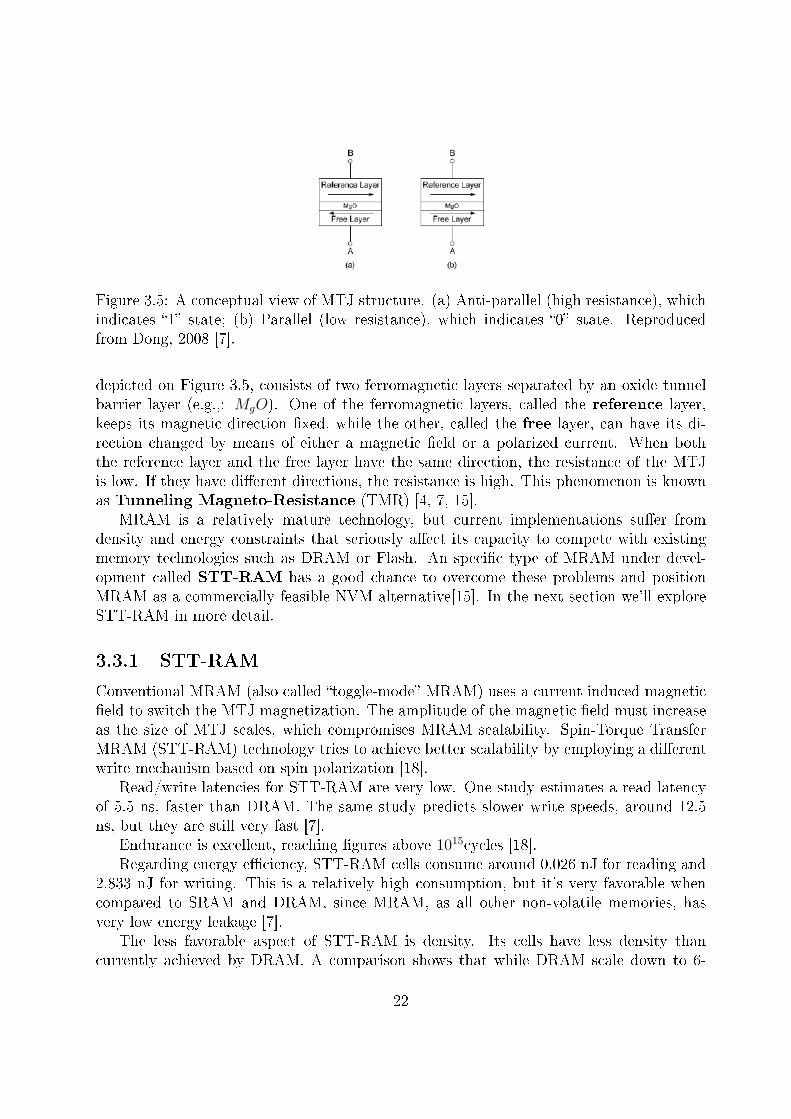
Figure 3.5: A conceptual view of MTJ structure. (a) Anti-parallel (high resistance), whichindicates �1� state; (b) Parallel (low resistance), which indicates �0� state. Reproducedfrom Dong, 2008 [7].
depicted on Figure 3.5, consists of two ferromagnetic layers separated by an oxide tunnelbarrier layer (e.g.,: MgO). One of the ferromagnetic layers, called the reference layer,keeps its magnetic direction �xed, while the other, called the free layer, can have its di-rection changed by means of either a magnetic �eld or a polarized current. When boththe reference layer and the free layer have the same direction, the resistance of the MTJis low. If they have di�erent directions, the resistance is high. This phenomenon is knownas Tunneling Magneto-Resistance (TMR) [4, 7, 15].
MRAM is a relatively mature technology, but current implementations su�er fromdensity and energy constraints that seriously a�ect its capacity to compete with existingmemory technologies such as DRAM or Flash. An speci�c type of MRAM under devel-opment called STT-RAM has a good chance to overcome these problems and positionMRAM as a commercially feasible NVM alternative[15]. In the next section we'll exploreSTT-RAM in more detail.
3.3.1 STT-RAM
Conventional MRAM (also called �toggle-mode� MRAM) uses a current induced magnetic�eld to switch the MTJ magnetization. The amplitude of the magnetic �eld must increaseas the size of MTJ scales, which compromises MRAM scalability. Spin-Torque TransferMRAM (STT-RAM) technology tries to achieve better scalability by employing a di�erentwrite mechanism based on spin polarization [18].
Read/write latencies for STT-RAM are very low. One study estimates a read latencyof 5.5 ns, faster than DRAM. The same study predicts slower write speeds, around 12.5ns, but they are still very fast [7].
Endurance is excellent, reaching �gures above 1015cycles [18].Regarding energy e�ciency, STT-RAM cells consume around 0.026 nJ for reading and
2.833 nJ for writing. This is a relatively high consumption, but it's very favorable whencompared to SRAM and DRAM, since MRAM, as all other non-volatile memories, hasvery low energy leakage [7].
The less favorable aspect of STT-RAM is density. Its cells have less density thancurrently achieved by DRAM. A comparison shows that while DRAM scale down to 6-
22
8F 2, STT-RAM currently doesn't scale below 37F 2, thus being 1.7 times less dense thanDRAM. STT-RAM supports MLC and 3D integration [7].
In 2005, Johan Åkerman published an article[1] proposing that MRAM could be the�universal memory� technology that would render obsolete all other components of memoryhierarchy (SRAM, DRAM, disks, �ash). Since then, papers on MRAM (including STT-RAM) often mention its possible future as �universal memory�. In practice, due to MRAMcurrent density limitations, it is not seen as a real replacement for DRAM as main memory(not to mention disks). Current ideas focus on using STT-RAM as an SRAM replacementfor building cache memories, due to its excellent read/write speeds, endurance, and muchsuperior energy e�ciency [7, 18].
3.4 Comparison Between Memory Technologies
So far, this study presented the most promising NVM technologies. We will now drawa comparison between each one of them as well as against the main current memoryhierarchy components: SRAM, DRAM, disks and �ash. In order to do this comparison,we will employ the following set of criteria:
1. Maturity: whether the technology is currently used in the market or it is in earlyor later research stages before being commercially mature.
2. Cell size: the cell size, using standard feature size (F 2).
3. Read Latency: the speed for reading values from a memory cell.
4. Write Latency: the speed for writing values to a memory cell.
5. Endurance: the number of write cycles that a memory cell endures before eventuallywearing out.
6. Energy: energy spent per bit access. Related to dynamic power.
7. Static Power: whether power needs to be spent while not accessing the memorydevice. This includes refreshing solid memory contents due to energy leakage orkeeping disks spinning to achieve lower access latencies.
8. Non-volatility: whether the memory technology is volatile or not.
Based on the data presented in the last sections of this work, table 3.1 compares thediscussed memory technologies against the de�ned set of criteria.
This concludes our survey of the new NVM technologies. In the next section we willexplore the potential impacts of such technologies on current memory systems.
23

Table 3.1: Comparison of memory technologies. The colors indicate how well each tech-nology scores against the speci�ed criteria. Green means a good score, red means a badscore, yellow is for scores in between. Data gathered from [4, 7, 15, 19, 20, 22].
24
4 Impacts on Memory Systems
No single memory technology of today can satisfy all requirements of low cost, high density,low energy, low latency and high endurance. For this reason, we use memory hierarchiesto obtain a performance similar to the faster technology and cost similar to the cheapertechnology. But one of the drawbacks of a sophisticated memory hierarchy is complexity.Today's memory systems evolved to extremely complex hierarchies, with many specializedlayers, which often interact in unexpected ways. There are some known cases of tech-niques that bring performance improvements to speci�c layers but result in overall systemdegradation [13].
With the current memory technologies approaching physical limits that will preventthem from scaling at the current pace (predicted by Moore's law), it will be necessary todevelop new technologies. The ideal future memory technology would have most (or all)of the bene�ts of cost, density, energy and latency, thus avoiding the need of too complexhierarchies. Recently, an article called such ideal technology �Universal Memory�, andpointed MRAM as its most promising example[1]. Unfortunately, as we have seen, none ofthe current technologies under development has the complete set of attributes to radicallysimplify memory systems.
Despite their inability to meet all �Universal Memory� requirements, these technologiespromise to improve current memory hierarchies, and allow memory systems to continuescaling up. In the last few years several papers have been published exploring the potentialuses of new non-volatile memories. In the next sections, we will present a survey on theirpredicted consequences.
4.1 Cache
On-chip and o�-chip processor caches are currently dominated by SRAM. These are thememory layers where MRAM is proposed to be used. MRAM, and more speci�cally STT-RAM, has excellent performance and endurance properties, but poor density when com-pared to DRAM. For this reason it is not currently considered �t for main memory or diskreplacement, both of which require great densities, and makes it a natural candidate forcaches.
4.1.1 MRAM as L2 and L3 cache
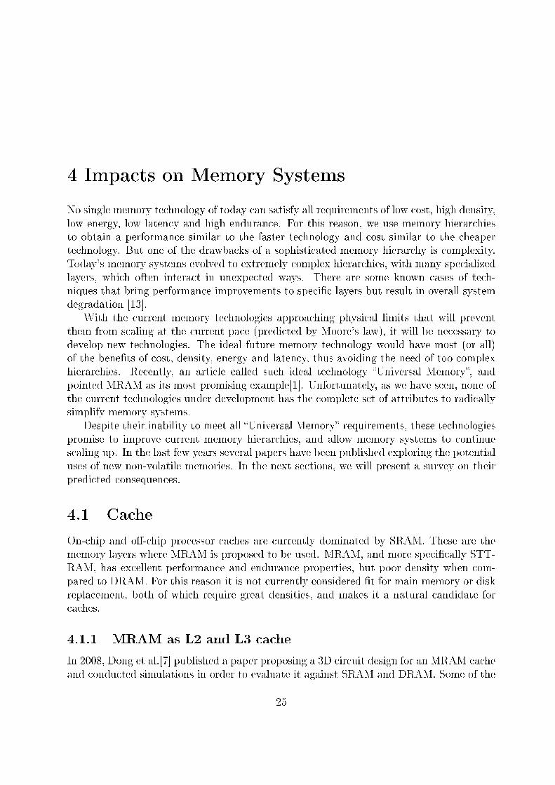
In 2008, Dong et al.[7] published a paper proposing a 3D circuit design for an MRAM cacheand conducted simulations in order to evaluate it against SRAM and DRAM. Some of the
25
Figure 4.1: MRAM L2 cache comparison against SRAM and DRAM. Extracted from [7].
results for MRAM as L2 cache are reproduced in Figure 4.1. The overall performance ofMRAM is not much di�erent from SRAM and DRAM, as seen in Figure 4.1-a, but the totalMRAM power consumption is strikingly superior, as shown in Figure 4.1-b. This di�erenceis rooted in the fact that MRAM is a non-volatile memory. The dynamic power (powerused to switch cell states) consumed by MRAM is actually superior to SRAM, but beingnon-volatile it needs no refresh and thus static power consumption becomes negligible whencompared to volatile memories. Dong et al. propose the usage of MRAM as L2 cache:
�(...) we conclude that using MRAM caches as the replacement of L2 cachescan save total power by 89% compared with SRAM caches and 70% comparedwith DRAM caches.�[7]
The same study also concluded that MRAM brings performance improvements as L3 cacheas well. The research team compared two simulated scenarios: (1) 2D processor with 1MBL2 SRAM cache; (2) 2D processor with 1MB L2 SRAM cache + 128MB MRAM L3 cache.The speedup ranged between 0.03% and 108%, and the best results were in benchmarkswith higher L2 miss rates, which are the most frequent under a current multi-task operatingsystem.
4.1.2 Hybrid SRAM/MRAM and SRAM/PCRAM as L2 and L3caches
Two papers were published in 2009 by Wu et al.[28, 29] proposing a hybrid cache designcombining SRAM and either MRAM or PCRAM into a single memory device. The essentialidea is to create a cache memory with two di�erent regions: a write region using SRAMand a read region using MRAM or PCRAM. Techniques are proposed for moving databetween the two regions. This architecture is called Read-Write aware Hybrid CacheArchitecture (RWHCA). These hybrid memories could be used as L2 and/or L3 caches.
26
They conclude, based on simulations, that a 2-layer 3D cache stack using RWHCA canimprove instructions per cycle (IPC) up to 18% and reduce power by 70% [29].
4.1.3 Fault-tolerant architecture for NVM caches
Elaborating on the previously mentioned papers, a study by Koh et al. [14] highlighted thefact that new NVM technologies, in particular MRAM, can have poorer yields than currenttechnologies, such as SRAM. As an example, the probability of a fault in a MRAM cell canbe 2 to 10x that of an equivalent SRAM cell[18]. Based on the higher densities of MRAM,the article proposes a cache architecture - called the salvage cache - that sacri�ces faultycache blocks to repair faults found in other blocks. They conclude that:
�(...) the salvage cache gives signi�cantly higher yields as well as higher e�ectiveassociativity. The latter results in better performance. We therefore concludethat the salvage cache structure is ideal for implementing a large set-associativeL2 cache with next-generation memory technologies.�[14]
4.2 Main Memory
Main memory today is implemented almost exclusively using DRAM. Most of current non-volatile main memory ideas involve the usage of PCRAM, alone or combined with othermemory technologies.
4.2.1 Pioneer work: �ash-based main memory
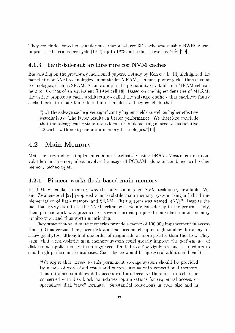
In 1994, when �ash memory was the only commercial NVM technology available, Wuand Zwanenepoel [27] proposed a non-volatile main memory system using a hybrid im-plementation of �ash memory and SRAM. Their system was named �eNVy�. Despite thefact that eNVy didn't use the NVM technologies we are considering in the present study,their pioneer work was precursor of several current proposed non-volatile main memoryarchitecture, and thus worth mentioning.
They state that solid-state memories provide a factor of 100,000 improvement in accesstimes (100ns versus 10ms) over disk and had become cheap enough to allow for arrays ofa few gigabytes, although of one order of magnitude or more greater than the disk. Theyargue that a non-volatile main memory system could greatly improve the performance ofdisk-bound applications with storage needs limited to a few gigabytes, such as medium tosmall high performance databases. Such device would bring several additional bene�ts:
�We argue that access to this permanent storage system should be providedby means of word-sized reads and writes, just as with conventional memory.This interface simpli�es data access routines because there is no need to beconcerned with disk block boundaries, optimizations for sequential access, orspecialized disk �save� formats. Substantial reductions in code size and in
27
Figure 4.2: Diagram of the high-level eNVy architecture. Extracted from Wu andZwaenepoel [27].
instruction pathlengths can result. For backwards compatibility, a simple RAMdisk program can make a memory array usable by a standard �le system.� [27]
Flash memory has some drawbacks when compared to DRAM: memory cannot be updatedin-place (a whole block must be erased before it can be reprogrammed), memory writesare much slower and endurance is more limited. To overcome these limitations, eNVyuses copy-on-write and memory remapping to provide normal in-place update semanticsand a battery-backed SRAM bu�er to hide the latency of �ash write access. They alsopropose a cleaning algorithm to reclaim space in the �ash array invalidated by copy-on-write operations. Figure 4.2 illustrates the high-level eNVy architecture [27].
4.2.2 PCRAM as main memory
In the 36th International Symposium on Computer Architecture (ISCA) that took placeat Austin in 2009, two di�erent papers proposed independent main memory systems basedon PCRAM.
4.2.2.1 Improving latency, energy and endurance through bu�er organizationand partial writes
Lee et al. [16] point out that DRAM has inherent scalability limits that will be reachedsoon, and propose a speci�c PCRAM array architecture to bring this technology withincompetitive range against DRAM as main memory. They argue that the array design mustaddress PCRAM's weak spots, such as write latency, high programming energy cost and�nite endurance. In order to achieve this goal, they propose two strategies, which theyhave evaluated through simulation:
1. Bu�er organization: reorganizing a single, wide bu�er into multiple, narrow bu�ersreduces both energy costs and delay. Their proposed design involves four 512B-widebu�ers instead of a single 2048B-wide bu�er. PCRAM delay penalties are reducedfrom 1.60x to 1.16x when compared to DRAM.
28
2. Partial Writes: data modi�cations are tracked, propagating this information fromthe L1 cache down to the bu�ers at the memory banks. When a bu�ered row is writescontent to the PCRAM array, only modi�ed data is written. As the number of bu�ersincrease, this solution becomes more e�cient. Using the four bu�ers described above,endurance improved up to 5.6 years in the best case [16].
4.2.2.2 Improving endurance and energy consumption through 3D stacking
The work of Zhou et al. [31] tackles the same problems with a di�erent circuit designproposal. Their paper point out the energy issues that plague DRAM today and howNVM technologies such as PCRAM can help overcoming them. They propose a 3D diestacked chip multiprocessor that puts together several processors and main memory onthe same chip. This is di�cult to achieve with DRAM today because such design requirestight power and thermal constraints that aren't �t for memories with high power leakage.They evaluate that the energy e�ciency of using PCRAM in this design can be 65% betterthan DRAM.
Although PCRAM has very low static energy consumption, they acknowledge, on theother hand, that PCRAM has endurance and dynamic power problems. In order to addressthese problems, they propose the following actions:
1. Removing redundant bit-writes: in a typical DRAM implementation, a writeupdates the contents of an entire row (also called a page), even when a single bitvalue changes. Changing this behavior to write only the changed bits requires anadditional read operation before writing. This wouldn't be an advantage for MRAMsince both read/write operations have similar latencies and energy consumption,but PCRAM reads are faster and more e�cient than writes, thus justifying thisstrategy. Simulations showed that endurance could increase between 3x-4.5x usingthis technique.
2. Wear leveling through row shifting: memory updates typically have high lo-cality, with some speci�c sets of bits changing much more often. This creates �hotspots� that fail much sooner than the rest. This can be addressed by periodicallyshifting the cells in a row to even out the wear. Simulations showed that endurancecan be improved around 3x with this change.
3. Wear leveling through segment swapping: row shifting brings some improve-ments to PCRAM, but not enough to achieve endurance to compete with DRAM.The problem is that some rows are written more often than others, thus failing sooner.In addition, they propose an additional wear leveling technique called segment swap-ping. It consists in periodically swapping memory segments of high and low writeaccesses. Simulations indicate that endurance can improve up to 10x by means ofthis change.
Their �nal conclusion is that using all these three techniques it is possible to increase the
29
lifetime of PCRAM main memory from 171 days to 13~22 years, while achieving energysavings of 65% when compared to DRAM [31].
4.2.2.3 Combining both approaches
In 2010, the authors of both papers [16, 31] published an article together proposing thecombination of both into a single approach [17].
4.2.3 Hybrid PCRAM-DRAM main memory
4.2.3.1 Qureshi et al. hybrid approach
Another paper, by Qureshi et al. [22] was presented in the ISCA '09, independentlyproposing a main memory system using a combination of PCRAM and DRAM. The authorsstress the importance of overcoming DRAM's charge issues that prevent the technologyfrom scaling in future years. They point out that PCRAM has the drawbacks of lowendurance and slow access when compared to DRAM. To address both issues, they proposea hybrid architecture where a DRAM bu�er is placed in the front of the main PCRAMstorage, as depicted in Figure 4.3. They evaluate that a bu�er of 3% of the size of themain storage can bridge the latency gap between DRAM and PCRAM.
In order to exploit this architecture, the following mechanisms are proposed:
1. Lazy-write organization: when a page fault is serviced, it is copied from disk tothe DRAM bu�er only, without incurring the write penalty of PCRAM. When thepage is evicted from the DRAM bu�er, if the page is dirty it is written to PCRAMstorage. This helps decreasing latency and improve endurance.
2. Line-level writes: to avoid writing a complete memory page (as DRAM does), onlydirty lines would be written in the PCRAM storage (this is similar to the �removingredundant bit-writes� technique mentioned before). This improves endurance.
3. Fine-grained wear-leveling: since memories tend to have high locality, some pagesare written more often, and can wear out sooner than the rest. They propose arotating mechanism between pages in order to distribute wear more evenly (this issimilar to �wear leveling through segment swapping� mentioned earlier). This helpsto increase endurance.
4. Page Level Bypass for write �ltering: some applications not only do not bene�tfrom the proposed architecture, but can even unnecessarily wear out the PCRAMstorage faster. A typical example are streaming applications, which access a largeamount of data with little reuse. The authors propose a Page Level Bypass (PLB)bit that can be enable by the operating system to indicate that the page should notbe written to the PCM storage after eviction from the DRAM bu�er, but merely bediscarded.
30
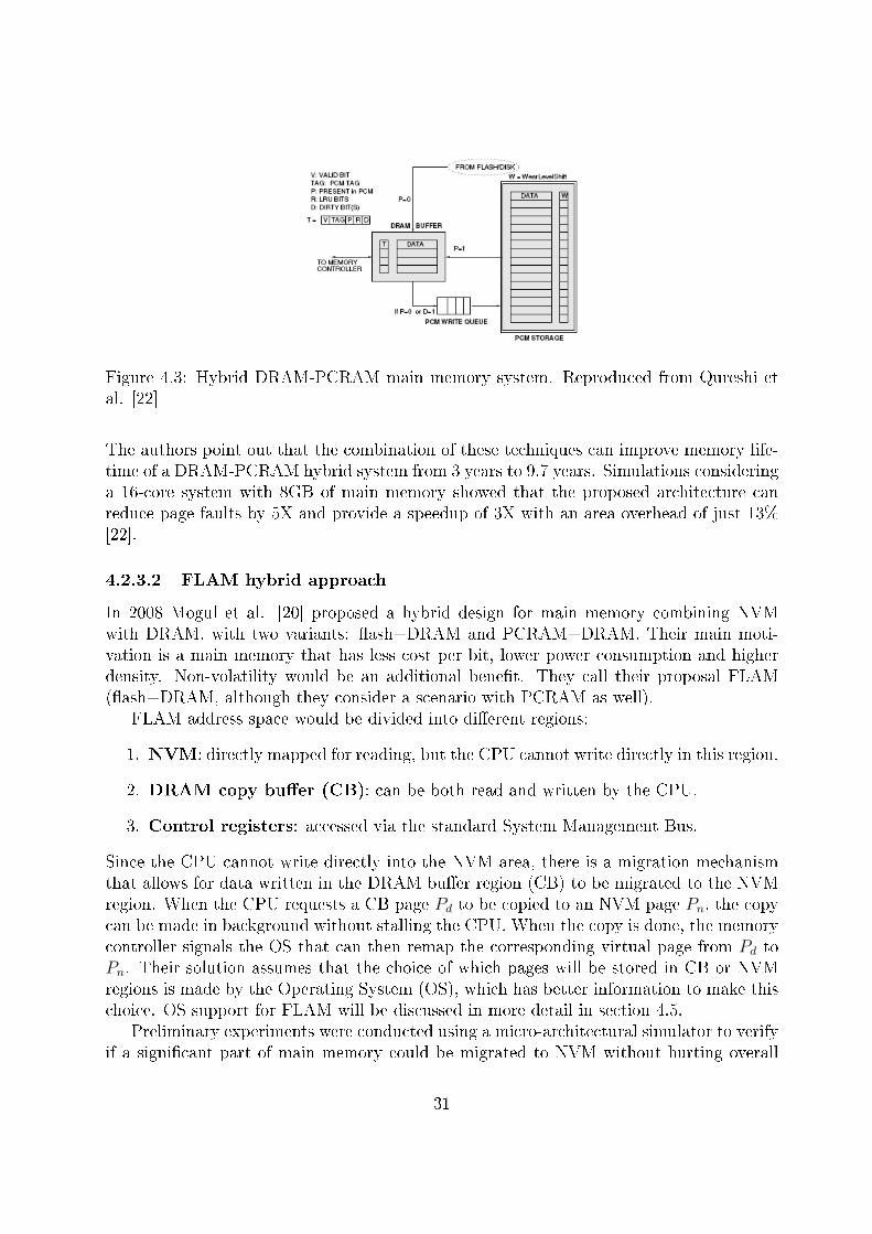
Figure 4.3: Hybrid DRAM-PCRAM main memory system. Reproduced from Qureshi etal. [22]
The authors point out that the combination of these techniques can improve memory life-time of a DRAM-PCRAM hybrid system from 3 years to 9.7 years. Simulations consideringa 16-core system with 8GB of main memory showed that the proposed architecture canreduce page faults by 5X and provide a speedup of 3X with an area overhead of just 13%[22].
4.2.3.2 FLAM hybrid approach
In 2008 Mogul et al. [20] proposed a hybrid design for main memory combining NVMwith DRAM, with two variants: �ash+DRAM and PCRAM+DRAM. Their main moti-vation is a main memory that has less cost per bit, lower power consumption and higherdensity. Non-volatility would be an additional bene�t. They call their proposal FLAM(�ash+DRAM, although they consider a scenario with PCRAM as well).
FLAM address space would be divided into di�erent regions:
1. NVM: directly mapped for reading, but the CPU cannot write directly in this region.
2. DRAM copy bu�er (CB): can be both read and written by the CPU.
3. Control registers: accessed via the standard System Management Bus.
Since the CPU cannot write directly into the NVM area, there is a migration mechanismthat allows for data written in the DRAM bu�er region (CB) to be migrated to the NVMregion. When the CPU requests a CB page Pd to be copied to an NVM page Pn, the copycan be made in background without stalling the CPU. When the copy is done, the memorycontroller signals the OS that can then remap the corresponding virtual page from Pd toPn. Their solution assumes that the choice of which pages will be stored in CB or NVMregions is made by the Operating System (OS), which has better information to make thischoice. OS support for FLAM will be discussed in more detail in section 4.5.
Preliminary experiments were conducted using a micro-architectural simulator to verifyif a signi�cant part of main memory could be migrated to NVM without hurting overall
31
system performance. In other words, they tried to establish if a signi�cant portion of mainmemory is used during long times just for reading and not for writing, using real workloads.The results varied depending on the workload, but they found that at least half of the mainmemory contents stay long periods without being written (above 15 secs), which pointsout that the proposed solution is worth further exploration [20].
4.2.3.3 BPRAM hybrid approach
Condit et al. [6]proposed a �le system (called BPFS) designed for byte-addressable, persis-tent RAM (BPRAM), a term they use to designate NVM technologies such as PCRAM.They argue that with NVM technologies the �le system should use direct-mapped memoryin the memory bus instead of block devices through the I/O subsystem. They proposeboth a �le system (BPFS) and the underlying hardware architecture for persistent mainmemory. In this section we will describe their proposal for the hardware and describe the�le system details in section 4.5.
They assume that PCRAM is presented to the system as DDR-compatible DIMMsavailable through the memory bus. A DRAM bu�er is present, and both PCRAM andDRAM addresses are directly mapped by the CPU for both reading and writing. It is alsoassumed that the PCRAM memory controller implements wear leveling and write failuredetection mechanisms. They suggest that wear leveling techniques proposed by Qureshi etal. [22] and Zhou et al. [31]could be used, along with failure detection mechanisms alreadyemployed by �ash memories.
Each row of the PCRAM array has a volatile bu�er for writes. In order to ensureatomicity for writes, each bu�er must be backed by a capacitor that guarantees that allin-progress writes are completed consistently in case of a power failure. Fortunately, theamount of energy needed is very low and such capacitors can be easily incorporated intothe memory module design.
The use of NVMs introduce an issue related with write ordering. Modern caches andmemory controllers can reorder writes on their way from CPU to memory. There arecache-coherence safeguards to ensure consistency across the hierarchy, but these safeguardsassume that both caches and main memory are volatile. Using NVM as main memory,when recovering from a power failure the main memory state might be inconsistent withthe cache. There are a number of simple solutions for this issue, such as not using the cache(write-through), �ushing all cache lines at each memory barrier or �ushing only the dirtycache lines, but all these solutions are prohibitive from the performance standpoint. Conditet al. propose a new mechanism called epoch barrier. An epoch barrier is determined atsoftware level and indicates a set of writes that are grouped together. When a new epochbarrier is issued, the memory controller must ensure that all writes from previous barrierswere already sent to persistent storage. The epoch barrier mechanism must be supportedby the memory controller and available to be used by software at upper layers [6].
More details on how the �le system uses the proposed hardware architecture are dis-cussed on section 4.5.
Simulations showed that BPFS using BPRAM should outperform NTFS using disks
32
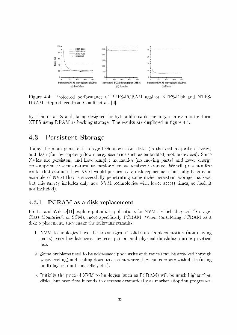
Figure 4.4: Projected performance of BPFS-PCRAM against NTFS-Disk and NTFS-DRAM. Reproduced from Condit et al. [6].
by a factor of 2x and, being designed for byte-addressable memory, can even outperformNTFS using DRAM as backing storage. The results are displayed in �gure 4.4.
4.3 Persistent Storage
Today the main persistent storage technologies are disks (in the vast majority of cases)and �ash (for low capacity/low-energy scenarios such as embedded/mobile devices). SinceNVMs are persistent and have simpler mechanics (no moving parts) and lower energyconsumption, it seems natural to employ them as persistent storage. We will present a fewworks that estimate how NVM would perform as a disk replacement (actually �ash is anexample of NVM that is successfully penetrating some niche persistent storage markets,but this survey includes only new NVM technologies with lower access times, so �ash isnot included).
4.3.1 PCRAM as a disk replacement
Freitas and Wilcke[11] explore potential applications for NVMs (which they call �Storage-Class Memories�, or SCM), more speci�cally PCRAM. When considering PCRAM as adisk replacement, they make the following remarks:
1. NVM technologies have the advantages of solid-state implementation (non-movingparts), very low latencies, low cost per bit and physical durability during practicaluse.
2. Some problems need to be addressed: poor write endurance (can be attacked throughwear-leveling) and scaling down to a point where they can compete with disks (usingmulti-layers, multi-bit cells , etc.).
3. Initially the price of NVM technologies (such as PCRAM) will be much higher thandisks, but over time it tends to decrease dramatically as market adoption progresses.
33

Figure 4.5: Projected 2020 characteristics of NVM (PCRAM). (SIO: start I/O). Repro-duced from Freitas and Wilcke 2008[11].
4. To be accessed as a block device, it may use existing I/O protocols such as SAS(Serial-Attached SCSI [Small Computer System Interface]), SATA (Serial AdvancedTechnology Attachment) or Fibre Channel. However, the authors state that theseprotocols will not allow to fully exploit NVM performance.
5. New protocols/interfaces should be created for accessing NVM, optimizing their usageas memory-mapped devices.
6. NVM will need runtime error detection and correction mechanisms, as used today inboth disks and DRAM.
7. As read accesses do not wear out PCRAM, read/write should be asymmetrical, theread unit being as small as a single word.
They also argue that NVM-based storage systems will be simpler and more predictable:
�The realization of very large, �attened memory address spaces and veryfast I/O devices will greatly improve speeds on practical applications, presum-ably greatly reducing the gap between peak and sustained performance. Also,the simple predictable behavior of SCM, compared to disks, will simplify per-formance tuning. It will eliminate many of the unexpected interactions seentoday when optimizing the memory and storage hierarchy.�[11]
The authors assume some projected characteristics of PCRAM (or similar NVM technol-ogy) by 2020, listed on �gure 4.5. Based on these characteristics, and the estimated I/Oneeds by 2020, they draw a comparison between disks and NVM for both compute-centricand data-centric workloads. The result is displayed on Figure 4.6. Their conclusion is thatNVM storage systems based on PCRAM can provide an e�ective storage system that is50-1,000 times the I/O performance of disk-based systems [11].
4.3.2 PCRAM or STT-MRAM as disk replacement
In an article called �After Hard Drives - What Comes Next� published in October 2009,Kryder and Kim [15] survey 13 NVM technologies (including PCRAM, MRAM and RRAM)
34
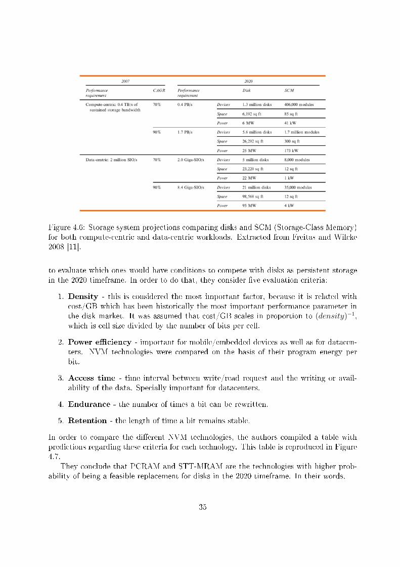
Figure 4.6: Storage system projections comparing disks and SCM (Storage-Class Memory)for both compute-centric and data-centric workloads. Extracted from Freitas and Wilcke2008 [11].
to evaluate which ones would have conditions to compete with disks as persistent storagein the 2020 timeframe. In order to do that, they consider �ve evaluation criteria:
1. Density - this is considered the most important factor, because it is related withcost/GB which has been historically the most important performance parameter inthe disk market. It was assumed that cost/GB scales in proportion to (density)−1,which is cell size divided by the number of bits per cell.
2. Power e�ciency - important for mobile/embedded devices as well as for datacen-ters. NVM technologies were compared on the basis of their program energy perbit.
3. Access time - time interval between write/read request and the writing or avail-ability of the data. Specially important for datacenters.
4. Endurance - the number of times a bit can be rewritten.
5. Retention - the length of time a bit remains stable.
In order to compare the di�erent NVM technologies, the authors compiled a table withpredictions regarding these criteria for each technology. This table is reproduced in Figure4.7.
They conclude that PCRAM and STT-MRAM are the technologies with higher prob-ability of being a feasible replacement for disks in the 2020 timeframe. In their words,
35
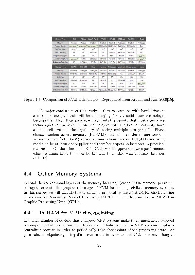
Figure 4.7: Comparison of NVM technologies. Reproduced from Kryder and Kim 2009[15].
�A major conclusion of this study is that to compete with hard drive ona cost per terabyte basis will be challenging for any solid state technology,because the ITRS lithography roadmap limits the density that most alternativetechnologies can achieve. Those technologies with the best opportunity havea small cell size and the capability of storing multiple bits per cell. Phasechange random access memory (PCRAM) and spin transfer torque randomaccess memory (STTRAM) appear to meet these criteria. PCRAMs are beingmarketed by at least one supplier and therefore appear to be closer to practicalrealization. On the other hand, STTRAMs would appear to have a performanceedge assuming they, too, can be brought to market with multiple bits percell.�[15]
4.4 Other Memory Systems
Beyond the conventional layers of the memory hierarchy (cache, main memory, persistentstorage), some studies propose the usage of NVM for some specialized memory systems.In this survey we will include two of them: a proposal to use PCRAM for checkpointingin systems for Massively Parallel Processing (MPP) and another one to use MRAM inGraphic Processing Units (GPUs).
4.4.1 PCRAM for MPP checkpointing
The huge number of devices that compose MPP systems make them much more exposedto component failures. In order to tolerate such failures, modern MPP systems employ acentralized storage in order to periodically take checkpoints of the processing state. Atpetascale, checkpointing using disks can result in overheads of 25% or more. Dong et
36
al. [8] proposed a checkpointing mechanism based on PCRAM. This mechanism assumesthat checkpoints can be local (speci�c to a node), where the node can reboot and recoverfrom the failure, or global, to be able to restore the complete system state in the caseof the removal of a node. In their proposal, 3D PCRAM DIMMs at each node are usedto store the local node checkpoints plus the checkpoints of two neighboring nodes. Theirsimulations indicate that this can enable MPP systems scaling up to 500 peta�ops to havecheckpoint overheads as low as 4% [8].
4.4.2 MRAM in GPU.
General-Purpose Graphic Processing Units (GPGPUs) have been used in modern comput-ers as auxiliary processors for compute-intensive applications. The CPU copies the data tobe processed to the GPGPU global memory and once the processing is complete, it copiesthe results back to the CPU. Today SRAM is used to implement most of the GPGPU globalmemories. Due to SRAM density limitations, the maximum size of these global memoriesare only 16 Kb. Satyamoorthy and Parthasarathy [23] propose an GPGPU design thatuses STT-MRAM as global memory, increasing by 4x the density with power savings of3.5x when compared to SRAM.
4.5 Operating System
Adding NVM to cache or persistent storage layers can be done without signi�cant changesto the Operating System (OS). On the other hand, if main memory was made persistent(or partially persisted) several changes would be required, since the OS decides what isstored in memory and what is persisted to the persistent storage. Particularly some of thehybrid PCRAM-DRAM approaches presented before [20, 6] require improvements on theOS level.
4.5.1 OS improvements to support FLAM.
In section 4.2.3 we presented FLAM [20], a hybrid DRAM+NVM approach for buildingmain memories. FLAM addressable space is divided in a DRAM region, that can be bothdirectly read/written by the CPU, and a NVM region, that the CPU can read but cannotwrite directly - instead, it needs to issue a request to the memory controller for copyinga page from the DRAM region to the NVM region. The criteria for deciding where toplace a page is based on its estimated-time-to-next-write (ETTNW): pages with a shortETTNW should be placed at the DRAM region, and pages with a long ETTNW shouldbe placed at the NVM region. The authors of the proposal argue that the OS shouldbe the responsible for deciding which pages will be placed in each region, since it hassome privileged information to support this decision. These are the di�erent pieces ofinformation that can help the OS to establish the ETTNW of a page:
37
� Page type: some page types, like stack pages and non-�le pages shared betweentwo processes, are bad candidates for NVM region. Others, such as code pages, arebetter candidates.
� File type: �les such as executables, libraries, network shares are mostly read-onlyand can be good candidates for NVM region.
� File reference modes: some OSs, like Microsoft Windows, have a �temporary �le��ag that can be applied to �les. Flags like this are a good indicator of �les thatshould not be placed at the NVM region.
� Application-supplied page attributes: certain large, memory-hungry applica-tions (e.g.,: databases) could be adapted to provide coarse ETTNW values for theOS.
� File usage history: the OS can track the actual time-to-next-write (TTNW) of all�les and use these historical data to estimate the ETTNW for each �le.
� Page usage history: in theory the OS could do the same tracking at page level. Inpractice, it would probably consume a great portion of DRAM to achieve this, whichwould be against the point of using FLAM (to save DRAM).
Preliminary simulations using this proposal showed that more than half of the DRAMpages have long TTNWs (above 15 secs) and could be moved to NVM to achieve energy,cost and density bene�ts [20].
4.5.2 BPFS �le system
Also in section 4.2.3, we presented a hybrid DRAM+PCRAM hardware called BPRAMthat supports BPFS, a �le system designed for byte-addressable, persistent memory [6].Now we will present the main characteristics of the �le system implementation at OS levelthat takes advantage of BPRAM hardware. The three design principles behind BPFS are:
� Direct memory mapping: BPRAM should be exposed directly to the CPU throughthe memory bus, instead of behind an I/O controller.
� Hardware support for ordering and atomicity: BPRAM hardware should pro-vide ordering and atomicity primitives to support software reliability guarantees.
� Short-circuit shadow paging: a technique called short-circuit shadow paging isused by the �le system to provide fast and consistent updates.
Most �le systems ensure reliability by using one of two techniques: write-ahead logging(also called journaling) or shadow paging. Journaling consists in writing the operationsthat will be performed to a separate location before updating the primary storage location.
38
It is the preferred method for disk-based �le systems since it is more e�cient for block-based devices. The drawback is that most writes must be done twice. Shadow pagingconsists in using copy-on-write to make all updates. The �le system is represented in theform a of tree, and when new data on a node is updated via copy-on-write, their parentsmust be successfully updated as well. When the changes propagate to the top of the tree,a single write �nally commits all changes to the �le system. They advocate the use of anspeci�c type of shadow paging, called short-circuit shadow paging, to harvest the bene�tsof using byte-addressable, persistent memory in place of block-based devices.
Simulations showed that BPFS using BPRAM should outperform NTFS using disksby an order of 2x and, being designed for byte-addressable memory, can even outperformNTFS using DRAM as persistent store. It is worth mentioning that, due to its design,BPFS has stronger reliability guarantees than current �le systems such as NTFS or ext3[6].
39
5 Conclusion
For almost 30 years, computer memory systems have been composed of SRAM for caches,DRAM for main memory and magnetic disks and �ash memory for persistent storage. Sofar, this design has enabled growth according to Moore's Law. However, limitations ofthese technologies threaten the ability to sustain this growth rate during the next decade,creating a �power wall�. In order to allow continuing growth, it will be necessary to developnew memory technologies.
As consequence, today we watch the emergence of new memory technologies thatpromise to change radically the landscape of computer memory systems. In this paper,we have presented three of the most promising new memory technologies under devel-opment: Phase-Change RAM (PCRAM), Magnetoresistive RAM (MRAM) and ResistiveRAM (RRAM). We have also surveyed the current proposals on how to apply them formemory systems. We are aware of other works that present emerging memory technologies,such as Burr et al.[4] and Kryder and Kim[15]. Nevertheless, to the best of our knowledge,this is the �rst work that has a comprehensive survey on how these technologies can a�ectthe di�erent layers of memory systems: cache, main memory, persistent storage, operatingsystem, etc.
Based on this analysis, we will now present our conclusions on the impacts these tech-nologies might have on memory systems.
The ideal future memory technology should be non-volatile, low-cost, highly dense,energy-e�cient, fast and with high endurance. Such ideal technology would be a �univer-sal memory�[1], eliminating the need for complex hierarchies in the memory subsystem.Unfortunately, as we've seen, none of the presented technologies has today all the neces-sary attributes to accomplish that. PCRAM is not fast enough and does not have thenecessary endurance. STT-MRAM cannot achieve high densities. RRAM has very limitedendurance. Until these issues are addressed, there will be no single �universal mem-ory� . If RRAM can be made to have high endurance, it can replace (with advantages) bothPCRAM and STT-MRAM for all levels: cache, main memory and disks, becoming a trulyuniversal memory. But this is still a challenge and there is no clear roadmap indicating ifthis will happen and when.
Actually, the introduction of these new technologies will probably result inmore com-plex hierarchies instead of simpler ones. MRAM can improve on-chip and o�-chip caches,but will require more complex cache management algorithms and maybe hybrid designs.PCRAM can be used to create a low-power, highly dense main memory, but will probablydemand hybrid designs that involve DRAM bu�ers. RRAM can be used for write-a-little-read-a-lot devices such as FPGAs and also as main memory in hybrid designs involving
40
DRAM bu�ers. All the three can potentially be used as persistent storage if their cost/bitgoes down enough, which might happen if they become widely adopted and manufacturedin large scale.
These technologies can allow the construction of memory chips that are non-volatile,low-energy, highly dense and with latency close to or better than current DRAM chips.This would be enough to avoid hitting a �power wall� associated with DRAM's currentlimitations. If their cost becomes low enough, they can also replace disks and �ash memoryas persistent storage, closing the latency gap between main memory and persistent storage.In summary, despite their inability to meet all �Universal Memory� requirements, thesetechnologies promise to improve current memory hierarchies, and allow memorysystems to continue scaling up.
At the beginning of this work, we discussed the bene�ts of creating energy-proportionalmemory systems. Since non-volatile memory (NVM) has extremely low static power con-sumption, if it is used in caches, main memory and persistent storage, energy-proportionalitywould be attained for the memory/storage subsystem. Since this subsystem is largely re-sponsible for the non-energy-proportional behavior of current servers, there would be hugeenergy savings, particularly for datacenter environments.
The adoption of one or more of these NVM technologies will bring signi�cant changesto memory systems. Some of these changes will be transparent to software applicationsand operating systems, but others will probably not. We still need to understand carefullythe impacts of such changes and how to prepare for them. This work tries to make acontribution in this direction.
We can foresee two interesting areas for future research:
1. Assuming that memory hierarchy will become more complex by incorporating emer-gent NVM technologies, we suggest more system-wide simulations in order to under-stand its system impact. Today most of the simulations are at component level.
2. Assuming that at some point in the future there will be a �Universal Memory� tech-nology, it would potentially change the complete memory hierarchy, re�ecting evenin operating systems, applications and programming models. We suggest the explo-ration of memory system models based on the assumption of Universal Memory.
41
References
[1] Åkerman, J. �Toward a Universal Memory�. Science 22: Vol. 308. no. 5721, pp. 508 -510, April 2005.
[2] Barroso, L. A., Hölzle, U. �The Case for Energy-Proportional Computing�. Computer40, 12, 33-37, Dec. 2007.
[3] Bruchhaus, R., Waser, R. �Bipolar Resistive Switching in Oxides for Memory Appli-cations� in S. Ramanathan (ed.), �Thin Film Metal-Oxides�, Springer, 2009.
[4] Burr, G. W., Kurdi, B. N., Scott, J. C., Lam, C. H., Gopalakrishnan, K., Shenoy, R.S. ``Overview of Candidate Device Technologies for Storage-Class Memory,'' IBM J.Res. & Dev. 52, No. 4/5, 449�464, 2008.
[5] Chua, L.O. �Memristor-the missing circuit element,� IEEE Transactions on CircuitTheory, vol. ct-18, (no. 5): 507-519, Sept. 1971.
[6] Condit, J., Nightingale, E. B., Frost, C., Ipek, E., Lee, B., Burger, D., Coetzee, D.�Better I/O through byte-addressable, persistent memory�. In Proceedings of the ACMSIGOPS 22nd Symposium on Operating Systems Principles (Big Sky, Montana, USA,October 11 - 14, 2009). SOSP '09. ACM, New York, NY, 133-146, 2009.
[7] Dong, X., Wu, X., Sun, G., Xie, Y., Li, H., Chen, Y. �Circuit and microarchitectureevaluation of 3D stacking magnetic RAM (MRAM) as a universal memory replace-ment�, Proceedings of the 45th annual Design Automation Conference, June 08-13,2008, Anaheim, California, June 2008
[8] Dong, X., Muralimanohar, N., Jouppi, N., Kaufmann, R., Xie, Y. �Leveraging 3DPCRAM technologies to reduce checkpoint overhead for future exascale systems�. InProceedings of the Conference on High Performance Computing Networking, Storageand Analysis (Portland, Oregon, November 14 - 20, 2009). SC '09. ACM, New York,NY, 1-12, November 2009.
[9] Drepper, U. �What Every Programmer Should Know About Memory�. November 21,2007. Captured from http://people.redhat.com/drepper/cpumemory.pdf, June 2010.
42
[10] Raoux, S., Burr, G. W., Breitwisch, M. J., Rettner, C. T., Chen, Y.-C., Shelby, R.M., Salinga, M. ``Phase-Change Random Access Memory: A Scalable Technology,''IBM J. Res. & Dev. 52, No. 4/5, 465�479, 2008.
[11] Freitas, R. F., Wilcke, W. W. �Storage-class memory: the next storage system tech-nology�. IBM J. Res. Dev. 52, 4, 439-447, July 2008.
[12] Ho, Y., Huang, G. M., Li, P. �Nonvolatile memristor memory: device characteris-tics and design implications�. In Proceedings of the 2009 international Conference onComputer-Aided Design (San Jose, California, November 02 - 05, 2009). ICCAD '09.ACM, New York, NY, 485-490, November 2009.
[13] Jacob, B., Ng, S. W., Wang, D. T. �Memory Systems: Cache, DRAM, Disk�. ISBN978-0-12-379751-3. Morgan Kaufmann Publishers, September 2007.
[14] Koh, C., Wong, W., Chen, Y., Li, H. �The Salvage Cache: A Fault-Tolerant CacheArchitecture for Next-generation Memory Technologies,� Proceedings of InternationalConference on Computer Design, Lake Tahoe, CA, October 2009.
[15] Kryder, M. H., Kim, C. S. �After Hard Drives - What Comes Next?�. IEEE Transac-tions on Magnetics, Volume 45, Issue 10, pp. 3406 - 3413, October 2009.
[16] Lee, B., Ipek, E., Mutlu, O., Burger, D. �Architecting phase change memory as ascalable DRAM alternative�. In International Symposium on Computer Architecture(ISCA), 2009.
[17] Lee, B. C., Zhou, P., Yang, J., Zhang, Y., Zhao, B., Ipek, E., Mutlu, O., Burger, D."Phase-Change Technology and the Future of Main Memory," IEEE Micro, vol. 30,no. 1, pp. 143-143, Jan./Feb. 2010.
[18] H. Li, Chen, Y. �An Overview of Non-Volatile Memory Technology and the Implicationfor Tools and Architectures�, Design, Automation & Test in Europe (DATE) 2009,pp. 731-736, 2009.
[19] Lewis, D. L., Lee, H.-H. S. �Architectural Evaluation of 3D Stacked RRAM Caches�.In IEEE International 3D System Integration Conference, 2009.
[20] Mogul, J. C., Argollo, E., Shah, M., Faraboschi, P. �Operating system support forNVM+DRAM hybrid main memory�. 12th Workshop on Hot Topics in OperatingSystems (HatOS XII), May 18-20, 2009.
[21] Moore, G. E. ``Cramming More Components onto Integrated Circuits,'' Electronics38, No. 8, 114�117, 1965.
[22] Qureshi, M. K., Srinivasan, V., Rivers, J. A. �Scalable high performance main memorysystem using phase-change memory technology�. In Proceedings of the 36th Annualinternational Symposium on Computer Architecture (Austin, TX, USA, June 20 - 24,2009). ISCA '09. ACM, New York, NY, 24-33, June 2009.
43
[23] Satyamoorthy, P., Parthasarathy, S. �MRAM for Shared Memory in GPGPUs�. Cap-tured from http://www.cs.virginia.edu/~sp5ej/MRAM.pdf, June 2010.
[24] Strukov, D. B. , Snider, G. S., Stewart, D. R., Williams, R. S. �The missing memristorfound,� Nature (London), vol. 453, pp. 80-83, 2008.
[25] Wang, F.Y. �Memristor for introductory physics�. arXiv:0808.0286 v1 [physics.class-ph], 4 August 2008, p.1-4. Captured from http://arxiv.org/abs/0808.0286, June 2010.
[26] Williams, R. S. �How We Found The Missing Memristor� IEEE Spectrum, vol. 45, pp.28-35, Dec. 2008.
[27] Wu, M., Zwaenepoel, W. �eNVy: a non-volatile, main memory storage system�. InProceedings of the Sixth international Conference on Architectural Support For Pro-gramming Languages and Operating Systems (San Jose, California, United States,October 05 - 07, 1994). ASPLOS-VI. ACM, New York, NY, 86-97, October 1994.
[28] Wu, X., Li, J., Zhang, L., Speight, E., Xie, Y. �Power and Performance of Read-writeaware hybrid caches with non-volatile memories.� Proceedings of Design Automationand Test in Europe (DATE), pp. 737-742, April 2009.
[29] Wu, X., Li, J., Zhang, L., Speight, E., Xie, Y. �Hybrid Cache Architecture withDisparate Memory Technologies.� In Proceedings of the 36th Annual internationalSymposium on Computer Architecture (Austin, TX, USA, June 20 - 24, 2009). ISCA'09. ACM, New York, NY, pp.34-45, June 2009.
[30] Yang, J. J., Pickett, M. D., Li, X. M., Ohlberg, D. A. A., Stewart, D. R., Williams,R. S. �Memristive switching mechanism for metal/oxide/metal nanodevices,� NatureNanotechnology, vol. 3, pp. 429-33, July 2008.
[31] Zhou, P., Zhao, B., Yang, J., Zhang, Y. "A Durable and Energy E�cient Main MemoryUsing Phase Change Memory Technology", The 36th International Symposium onComputer Architecture, pp. 14-23, June 2009.
44


![Phase-change random access memory: A scalable …signallake.com/innovation/raoux.pdfPhase-change random access memory: A scalable technology S. Raoux ... [or phase-change RAM (PCRAM)]](https://img.dokumen.tips/doc/110x75/5ac82a627f8b9a51678bfdc4/phase-change-random-access-memory-a-scalable-random-access-memory-a-scalable.jpg)