Embed Size (px)
Citation preview
AD-A145 356 ROUTING THE POWER AND GROUND WIRES OR A VLSI CHIP(U)
MASSACHUSETT ANS OF TECH CAMBRIDOE LAB FOR COMPUTER
SCIENCE A SMOULTONJUL 84 MITCsTR-322UNRLASSIFIED 000480-C0622 0G9/3 N
11111 ~ ' j* ? 2.5
1111.5 1=6
MICROCOPY RESOLUTION TEST CHARTNATIONAL. BUREAU 01 ST.NA6S -1963-.'
VeLABORATRFO R MASCUET
INSTITUTE O
COMUE CEC PTTCNLG
LfllCS'R-2
ROTNGTE O E
AN RUN IEONAVSICI
An F2V tmmt o lo
'I1,rIj(1 ""~p)td h h )A i~ d a cd R saclcoc .,A c ) (c ,IlIm i )f)tc s , vsm nt rdh
fo~~~ -~ I ( !!-Adft Pbt&c . )rh~td -
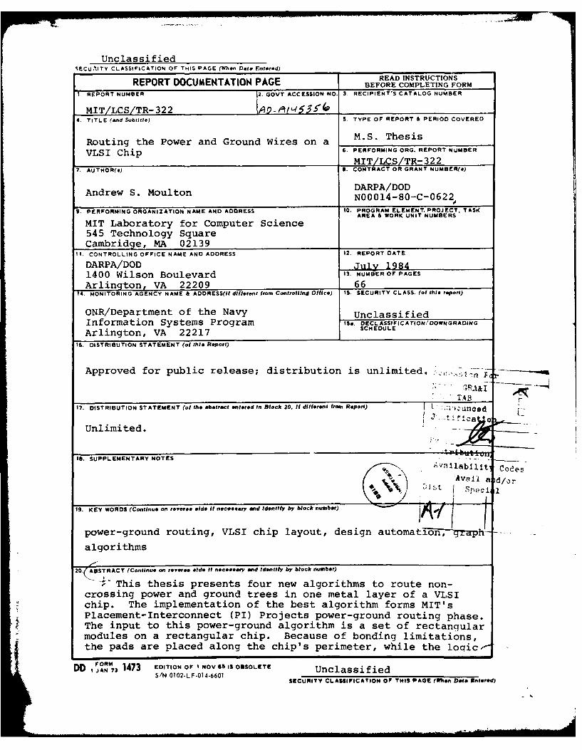
UnclassifiedSECU,' ITY CLASSIFICATION OF THIS PAGE (When Data Entered)
REPORT DOCUMENTATION PAGE READ INSTRUCTIONSBEFORE COMPLETING FORM
I. REPORT NUMBER 2. GOVT ACCESSION NO. 3. RECIPIENT'S CATALOG NUMBER
MIT/LCS/TR-322 ____ -_ A_/q 5"_ _ (04. TITLE (and Subtitle) 5. TYPE OF REPORT & PERIOD COVERED
Routing the Power and Ground Wires on a M.S. Thesis
VLSI Chip 6. PERFORMING ORG. REPORT NUMBER
MIT/LCS/TR-3227. AUTHOR(s) S. CONTRACT OR GRANT NUMBER(S)
DARPA/DODAndrew S. Moulton N00014-80-C-0622
9. PERFORMING ORGANIZATION NAME AND ADDRESS 10. PROGRAM ELEMENT. PROJECT, TASKAREA & WORK UNIT NUMBERS
MIT Laboratory for Computer Science545 Technology SquareCambridge, MA 02139
11. CONTROLLING OFFICE NAME AND ADDRESS 12. REPORT DATE
DARPA/DOD July 19841400 Wilson Boulevard 13. NUMBER OF PAGES
Arlington, VA 22209 6614. MONITORING AGENCY NAME & ADDRESS(f different from Controlling Office) IS. SECURITY CLASS. (of this report)
ONR/Department of the Navy UnclassifiedInformation Systems Program Isa. DECLASSIFICATfON'DOWNGRADING
Arlington, VA 22217 SCHEDULE
16. DISTRIBUTION STATEMENT (of this Report)
Approved for public release; distribution is unlimited. '-:';.n
TAB17. DISTRIBUTION STATEMENT (of the abstract entered In Block 20, It different from Report) IL~lun ed
Unlimited.
10. SUPPLEMENTARY NOTES ...lb lt-t" labllitoC~e
Z"J Avail l d/or
19. KEY WORDS (Continue on reverse aide It necessary end identify by block number)
power-ground routing, VLSI chip layout, design automation, --.. h-
algorithms
20. ABSTRACT (Continue on reveres side It necesesry end Identify by block number)
" ~This thesis presents four new algorithms to route non-
crossing power and ground trees in one metal layer of a VLSIchip. The implementation of the best algorithm forms MIT'sPlacement-Interconnect (PI) Projects power-ground routing phase.The input to this power-ground algorithm is a set of rectangularmodules on a rectangular chip. Because of bonding limitations,the pads are placed along the chip's perimeter, while the loqic.
DD IFORM 1473 EDITION OF 1 NOV 6S.S OBSOLETE
S/01"MA4.0 UnclassifiedS/N 0102-LF-014-6601 SECURITY CLASSIFICATION OF THIS PAGE (MYlen Dots Entered)
UnclassifiedSECJmlTY CLASSIFICATION OF THIS PAGE (When Data Entee.d)
20. continued.
,,modules are placed in the interior. In constructing the power-ground layout, the algorithm first lays a ground ring between thepads and the chip's perimeter, then a power ring between thelogic modules and the pads. Next, a tree of wires connects theground pad with the logic modules' ground connection points.Then, starting at various points on the power ring, severalbranches of wires connect the power ring to the logic modules'power connection points. A tree-traversal algorithm then usesthe modules' current requirements to determine how much currentwill flow through each power-ground wire during the chip'soperation. An algorithm then widens each wire to the width ap-propriate for carrying that current.
UnclassifiedSECURITY CLASSIFICATION OF THIS PAGE(Whfl Date Entet~d)
ROUTING TIlE POWEI AND GROUND WIRES ON A VLSI CHIP
by
ANDREW STROUT MOULTON
submitted to the
DEPARTMENT OF ELECTRICAL ENGINEERING AND COMPUTER SCIENCE
in partial fulfillmentof the requirements for the degree of
MASTER OF SCIENCE
at
MASSACHUSETTS INSTITUTE OF TECHNOLOGY
May, 1984
© Massachusetts Institute of Technology, 1984
This research was supported by the Defense Advanced Research Projects Agencyunder Contract No. N00014-80-C-0622, by the Air Force under Contract No. AFOSR-F49 62 0-8 1A00 54 , and by General Electric.
Signature of Author -A ,i o 1., 522S.t ..Department or Electrical Engineering and Computer Science
May 25, 1984
Certified by-Prof. liondd Linn Rivest
Thesis Supervisor
Accepted byProt Arthur C. Smith
Chairman, DegnIrtmn(,it Committee
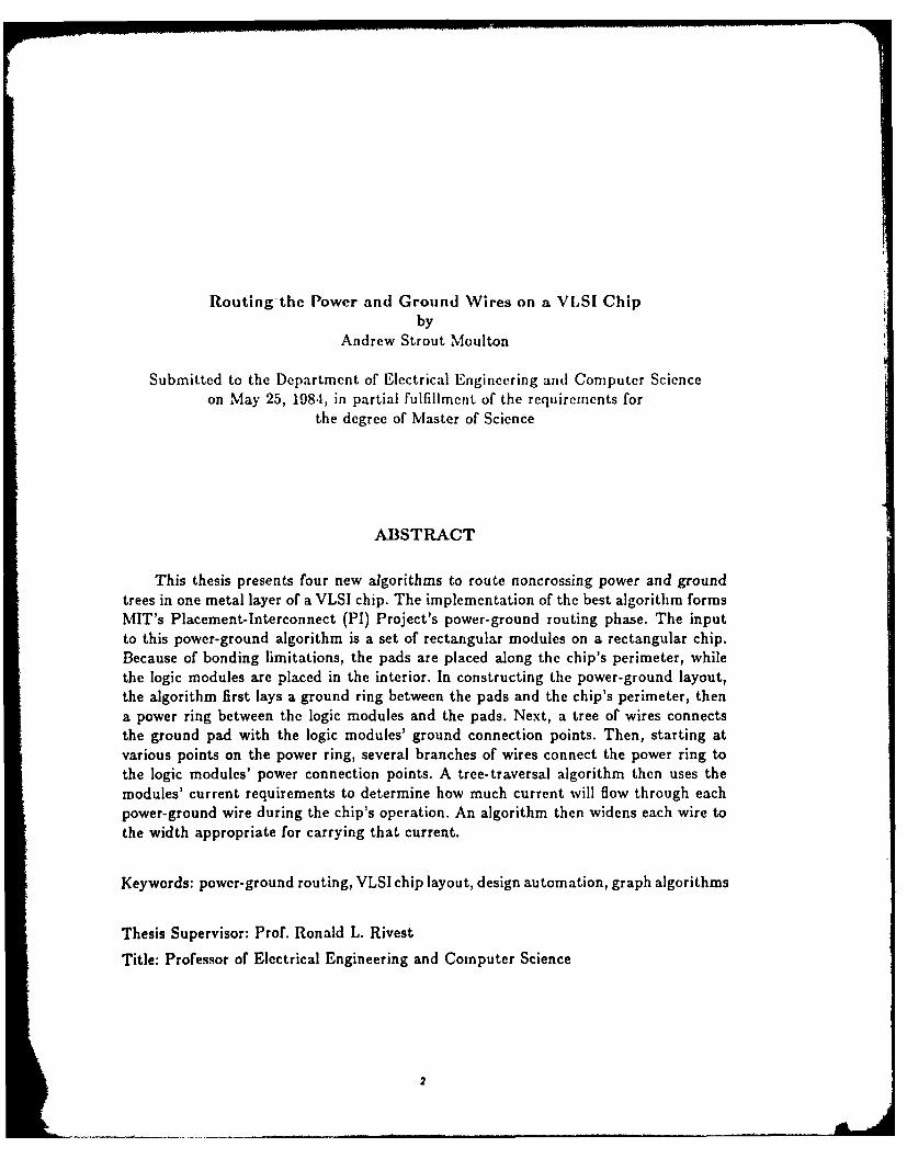
Routing the Power and Ground Wires on a VLSI Chipby
Andrew Strout Moulton
Submitted to the Department of Electrical Engincering and Computer Scienceon May 25, 19841, in partial fulfillment of the requiremecnts for
the degree of Master of Science
ABSTRACT
This thesis presents four new algorithms to route noncrossing power and groundtrees in one metal layer of a VLSI chip. The implementation of the best algorithm formsMIT's Placement- Inte rcon nect (PI) Project's power-ground routing phase. The inputto this power-ground algorithm is a set of rectangular modules on a rectangular chip.Because of bonding limitations, the pads are placed along the chip's perimeter, whilethe logic modules are placed in the interior. In constructing the power-ground layout,the algorithm first lays a ground ring between the pads and the chip's perimeter, thena power ring between the logic modules and the pads. Next, a tree of wires connectsthe ground pad with the logic modules' ground connection points. Then, starting atvarious points on the power ring, several branches of wires connect the power ring tothe logic modules' power connection points. A tree-traversal algorithm then uses themodules' current requirements to determine how much current will flow through eachpower-ground wire during the chip's operation. An algorithm then widens each wire tothe width appropriate for carrying that current.
Keywords: power-ground routing, VLSI chip layout, design automation, graph algorithms
Thesis Supervisor: Prof. Ronald L. Rivest
Title: Professor of Electrical Engineering and Computer Science
2

ACIK NOW IEI)GMENTS
I would like to thank my thesis advisor for first introducing me to the power-groundproblem, for making many helpful suggestions, and for guiding my research toward theproblem's solution.
I am grateful to all members of the Placement-Interconnect Research Group. Ina close-knit effort such as PI, the quality of one's work depends upon the quality ofeveryone else's. It is important to have a group that applies the time, effort, and abilityto produce high-quality work.
I wish to acknowledge the generosity of the organizations that contributed to myfinancial support, and I appreciate MIT and the Laboratory for Computer Science formaking so many facilities available to me.
I am thankful for the many times the support staff of the Theory of ComputationGroup came to my aid. Also, I am indebted to the people who read the many drafts ofthis thesis and gave me many helpful suggestions on my writing style.
Finally, I would like to thank my family for their constant and dependable love,understanding, confidence, and support.
3i
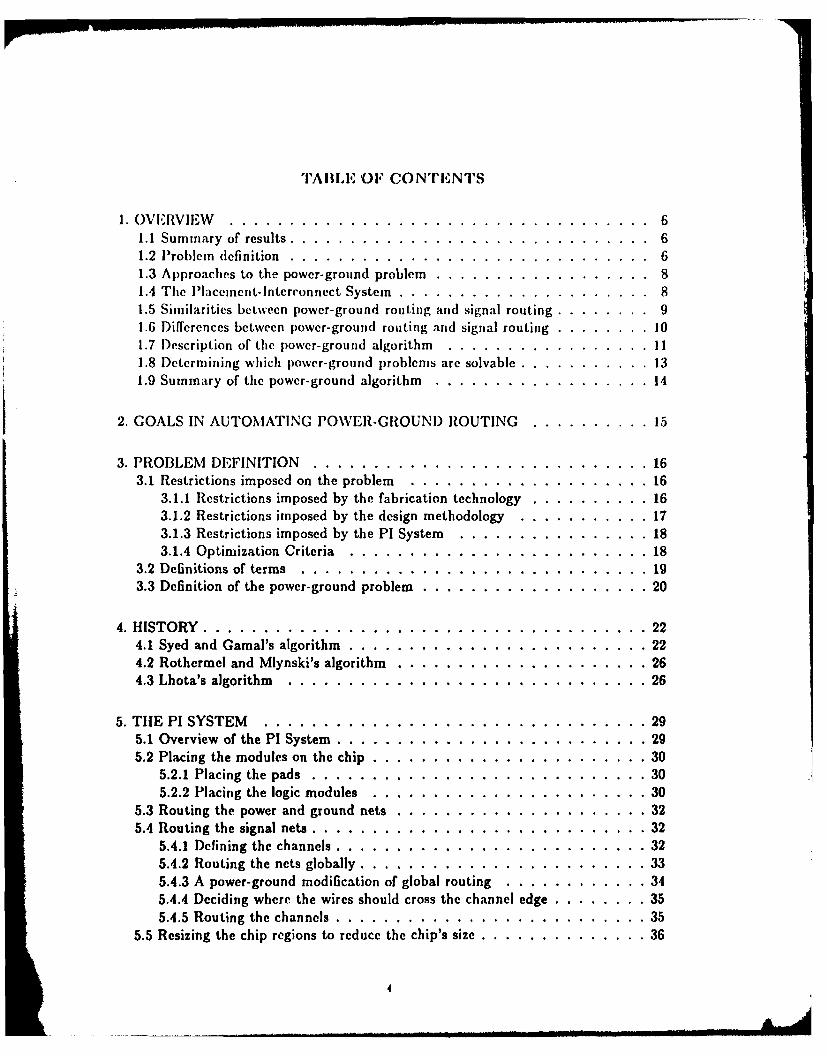
'ABLE, OF CONTr-ENTS
1. OVERVIEW . . . . . . . . . . . . . . . . . . . . . . . . . . . . . . . . . . . 61.1 Summary of results 61.2 Problem definition ..... 61.3 Approaches to the power-ground problem ..... .................. 8
1.4 The Placeinent-Intcrconnect System ..... ..................... 81.5 Similarities between power-ground routing and signal routing ........... 91.6 Differences between power-ground routing and signal routing .......... 101.7 Description of the power-ground algorithm .... ................. 111.8 Determining which power-ground problems are solvable .............. 131.9 Summary of the power-ground algorithm ...... .................. 14
2. GOALS IN AUTOMATING PO\VER-GROUND ROUTING ............. 15
3. PROBLEM DEFINITION ...................................... 163.1 Restrictions imposed on the problem ...... .................... 16
3.1.1 Restrictions imposed by the fabrication technology ............. 163.1.2 Restrictions imposed by the design methodology ... ........... 173.1.3 Restrictions imposed by the PI System ..... ................ 183.1.4 Optimization Criteria ....... ......................... 18
3.2 Definitions of terms ........ ............................. 193.3 Definition of the power-ground problem ..... ................... 20
4. HISTORY ......... ..................................... 224.1 Syed and Gamal's algorithm ....... ......................... 224.2 Rothermel and Mlynski's algorithm ...... ..................... 264.3 Lhota's algorithm ........ .............................. 26
5. THE PI SYSTEM ......... ................................ 295.1 Overview of the PI System ....... .......................... 295.2 Placing the modules on the chip ...... ....................... 30
5.2.1 Placing the pads ........ ............................ 305.2.2 Placing the logic modules ...... ....................... 30
5.3 Routing the power and ground nets ...... ..................... 325.4 Routing the signal nets ....... ............................ 32
5.4.1 Defining the channels ....... .......................... 325.4.2 Routing the nets globally ...... ........................ 335.4.3 A power-ground modification of global routing ................ 345.4.4 Deciding where the wires should cross the channel edge .......... 355.4.5 Routing the channels ....... .......................... 35
5.5 Resizing the chip regions to reduce the chip's size .............. 36
4
6. I)UR ALOITHMIC MICTllOI)S TO GIROV NONCROSSING I'iIES . . . 386.1 Growing the trees sequetitially, one after the other ............. 38
6.1.1 Successively rerouting branchesto shorten the trees' comi)ined length .... ................. 39
6.1.2 Constructing one tree, then a forest of trees .................. 426.2 Constructing the trees concurrently, one branch at a time ........... 436.3 Drawing a llamiltonian cycle through the modules,
then constructing the trees ...... .......................... 166.3.1 Using the Hlamiltonian cycle to divide the chip into regions ...... .. 166.3.2 Defining distance from one module to another ................ 476.3.3 Finding a short laniltonian cycle ..... ................... 486.3.4 Routing the llamiltonian cycle ..... ..................... 196.3.5 Routing the VDD and GND nets ...... .................... 526.3.6 Advantages and disadvantages of using the Iamiltonian cycle . . .. 54
6.4 Laying two rings to connect the pads, then growing the treessequentially to connect the logic modules ..... .................. 546.4.1 Laying two rings to connect the pads .... ................. 546.4.2 Growing the trees sequentially to connect the logic modules ...... .556.4.3 Advantages and disadvantages of laying the rings
and growing the trees sequentially ..... ................... 57
7. TIlE TREE-TRAVERSAL ALGORITHMTIIAT DETERMINES WIRE WIDTH ..... ...................... 58
8. EXPERIMENTAL RESULTS ...... .......................... 61
9. PROBLEMS FOR FURTHER RESEARCH .... ................... 64
10. CONCLUSIONS ....... ................................. 65
11. BIBLIOGRAPHY ....... ................................ 66
1. OVERVIEW
1.1. Sumnmry or results
This thesis presents new algorithmns that route power and ground wires to the
modules of a custom-designed VLSI chip. The algorithms produce two noncrossing,
interdigilated trees of metal wires, each wire being wide enough to carry the current
that will flow through it during the operation oF the chip. The LISP implementat ion
of these algorithins forms one part of the Placeinent-Interconnect (PI) System under
development at Massachusetts Institute of Technology.
1.2. Problem definition
The general power-ground problem is to lay wires that connect every power
connection point on the modules to the power pad(s) and every ground connection
point to the ground pad(s). Each wire must be wide enough to carry the current that
will flow through it during the operation of the chip. Any layout that meets these
specifications is a solution to the problem.
The power-ground problem is part of the larger problem of automating chip layout.
Developments in VLSI technology have greatly increased the number of modules and
nets on a chip. The time and complexity of laying the wires that interconnect the
modules have aroused interest in automating the layout process.
This thesis mostly deals with the design of layouts for chips that have one power
pad, one ground pad, and one metal layer. However, Section 1.7, paragraph 4, describes
how multiple power-ground pads could connect to the rings that route the signal pads.
Electrical considerations make it highly desirable to lay the power-ground wires
entirely in the metal layer. For example, reliable connections are particularly important
in the power and ground nets because proper operation of the chip components depends
critically on a stable voltage difference between power wires and ground wires. Also,
the amount of current in the power-ground wires is often large. A layout of metal wires
provides more reliable connections and can handle larger amounts of current than a
layout of wires that shift between layers.
6
On ihe other hand, with only a single layer of iieal availale, using only netal
imposes Ilie restriction that wires of one iet cannot cross those of the olher net. For
one wire to cross another without connecting to it, the first wire would have to shift
to another laver, run under the other wire, and then shift back to the original layer.
The metal area takeni up by power-ground w ires should be as small as possible.
The reason for this is that decreasing chip size is one goal of VLSI design, and wires
take up so uiuch of the chip area that decreasing wire area significantly decreases
chip size. Also, using less metal area for power-ground routing leaves more for signal
routing, enabling the signal-routing algorithms to run more eiliciently and produce
better results.
Describing a specific power-ground problem instance involves describing the
modules, power net, and ground net of the chip. A module is a collection of various chip
components. For the power-ground problem, the most important facts about a module
are the size and location of the rectangular region it occupies, the amount of current
it will use, and the locations of its connection points. A connection point is a point,
usually on the module's perimeter, where the module can connect to wires outside the
module. A power connection point should connect to a wire running to the power pad,
and a ground connection point should connect to a wire running to the ground pad.
The power net is a set of connection points that are to be connected by wires in the
power-ground layout. These power connection points lie on all modules of the chip.
The ground net is the set of all ground connection points. Chapter 3 describes in more
detail the facts, forms, and assumptions in a description of a specific power-ground
problem.
When regarded as a problem in graph theory, the power-ground problem is the
problem of finding two short, noncrossing Steiner trees in the plane. In this model,
connection points and wires are equivalent to points and edges in the plane. An
edge's cost is defined to be the amount of metal used by the corresponding wire. The
power-ground trees are regarded as Steiner trees because the fabrication technology
allows connections between wires at locations other than modules' connection points.
7
1.3. Approches to tche powr-ground p~roblel
Chapter I presents other researchers' work on the power-ground problem. Sycd
and El Canal keep the power and ground trees from crossing by imposing trallic rules
governing where wires may run in each channel. Rothernial anid Mlynski grow the
power tree from one side of the chip and the ground tree from the other. Lhota studies
the rela',ed problem in graph theory of finding two noncrossing spanning trees. i s
"Saran-Wrap" solution produces trees within 3/2 of optimal.
Chapters 6 and 7 present the main original results of this thesis. Four new solution
techniques arose during this research in the power-ground problem. With respect to
the goals of running efficiently and producing high-qu ality output, the fourth solution
technique seems to be the best. The four techniques are:
Routing one tree, then routing the other tree without crossing the first,
then modifying both in an attempt to find shorter trees.
* Routing the two trees in parallel, one branch at a time. In deciding which
branch to route next, this technique looks ahead and routes the trees so
that the final result will be short trees.
" Keeping the two trees from crossing by drawing a 11amiltonian cycle
through the modules, routing one tree inside and the other outside the
cycle.
" Using bus rings to connect the pads, then routing one tree to the logic
modules, then routing a forest of small trees to the logic modules.
1.4. The Placement-Interconnect System
The Placement-Interconnect (PI) Research Group under Prof. Ronald Rivest at
Massachusetts Institute of Technology is developing algorithms to solve theoretical and
practical problems that arise in designing chip layout. This group's work is described
in [R182]. This group's goal is to automate the entire placement and interconnect
phases of chip design, producing high-quality output with a minimum amount of human
interaction. The chip design follows the simplified rules of Mead and Conway [MCSO]
NA
as applied to standard single-layer metal, n-channel metal-oxide-semiconductor (tiMOS)
fabrication technology. In this thesis, 1 refers to a computer system developed t)y
this research group that implements the algorithms to do module placement and
interconnect.
The input to PI specifies a set of rectangular modules and a set of nets. The input
information for each module is the module's dimensions, its current requireirients, and
the locations of its connection points.
To produce the final chip design, PI goes through four steps:
* Placing the modules (including the pads) on the chip.
* Routing the power and ground nets.
* Routing the signal nets.
* Compacting the placement of the modules and wires to reduce the chip's
size.
This thesis describes algorithms developed for PI's second phase, which routes
the power and ground nets. This phase occurs after P1 has placed the modules and
before it has laid any signal wires. The power-ground algorithms are compatible with
the rest of P1, work within its restrictions and assumptions, and use its data base
and algorithms. Therefore, many aspects of PI, such as its signal-routing techniques,
have greatly influenced the form and scope of the power-ground algorithms. Chapter 5
describes P1 in more detail.
1.5. Similarities between power-ground routing and signal routing
Power-ground routing is in many respects like signal routing. In both routings,
wires connect a set of connection points on various modules. Both routings have the
goal of keeping the wire area small. In PI, both routings route a net by laying a short
Steiner tree of wires that spans the net's connection points.
I)r. Alan I a ratz designedI Pl's algorit ll, that constructs the Steiner trees. A more
&-tailed de ,riptloll of this algorithin is ill Sec tion 5.A.2 anld a full presentation is il
[1181]. To route a net wit i 71 connection points, the algorithn builds a graph where
each connection point is represented by a vertex. It then adds to this graph vertices that
represent in terinediat e points lying in free, unoccupied regions of the chip (see Section
5.A.2, paragraph 4, for the exact placement of these points). The distance between a
pair of vertices reflects the (listance between the represented points. There are initially
?i basis groups, each consisting of one connect ion point vertex.
Paths are made to grow simiultaneously in all directions from all basis groups. For
each basis group, the path grows by adding the vertex that is closest to that basis
group. In this aspect, the algorithm is similar to I)ijkstra's algorithm for finding a
single-source shortest path.
As soon as two paths meet, forming a bridge between two basis groups, the vertices
of the two groups plus the vertices along the bridge form a new basis group that
replaces the two old ones. In the next step, paths grow from each of the n - I remaining
basis groups. The process repeats until there is just one basis group. Reconstructing
each bridge that connected two basis groups builds a Steiner tree that connects the n
connection point vertices.
1.6. Differences between power-ground routing and signal routing
One difference between power-ground routing and signal routing is that a wire of
one signal net can switch layers to cross under a wire of another signal net whereas a
power wire cannot cross under a ground wire, under the assumption that there is only
a single metal layer available.
The difficulties with one wire crossing another are reflected in the cost the
algorithms associate with each edge. A change in the cost rules results in algorithms
that grow noncrossing Steiner trees. For signal routing, if an edge represents a wire
that crosses another wire, the edge's cost is increased by an amount that reflects the
disadvantages of shifting to another layer. For power-ground routing, the crossing cost
10
is set so high that the Steiner tree algorithms, looking for cheap paths, will never
choose an edge representing a wire that gives rise to a crossing.
Another difference between power-ground routing and signal routing is that tile
current in signal wires is typically siiall enough to permit the wire's width to be the
minimum allowed by the fabrication technology whereas the larger currents flowing
through power-ground wires require wire widiths to be determined individually in each
case.
This paragraph describes the technique, presented in Chapter 7, for determining
how wide each power-ground wire should be. The Steiner tree algorithiiis produce
complete trees of minimum-width wires. The trees' roots are the power and ground
pads, and the leaves are the modules' connection points. Using each module's current
requirement, a tree-traversal algorithm calculates how much current flows through each
wire. The design rules are then used to compute the required width for each wire.
The PI Research Group is developing a resizer that modifies the placement of
modules and wires to accomplish any of three tasks:
* Widen power-ground wires.
0 Provide more room for signal routing.
0 Compact a complete layout of modules and wires.
The power-ground algorithms use the resizer to make each power-ground wire grow
to its required width. For each wire, input to the resizer consists of one side of the wire,
the other side of the wire, and the required width of the wire. The resizer modifies the
placement of the sides of the wire so that they are separated by the required distance,
producing a wire of the appropriate width.
1.7. Description of the power-ground algorithm
This section describes the original power-ground routing techniques developed to
implement P's power-ground routing phase.
i1
Il's 1ethod of placilig iiuoduhles inlliences tie power-ground layout.. I'1 places along
the chip's perimeter the power, ground, and signal pads, signal pads being the modules
that carry communications to and from the chip. PI places in the chip's interior the
logic modules, which are the modules that, perform the desired logical or functional
operations.
This placement makes it. natural to separate laying power-ground wires to the
signal pads fromi laying wires to the logic imouiles. There are two reasons for this:
" The placement of the signal pads is uniform.
* The current requirements of signal pads are often much greater than
those of logic modules.
Laying wires to the signal pads creates a uniform pattern of wires. One ground
wire, called the ground ring, runs from the ground pad along the chip's perimeter,
between the signal pads and the chip's edge. One power wire, called the power ring,
runs from the power pad along the inside edge of the signal pads, between the logic
modules and the signal pads. This power ring does not run along the inside edge of the
ground pad, but leaves a gap there to give the ground pad access to the logic modules.
Short wires connect the rings to the connection points on the signal pads. The result is
that for the signal pads the rings connect every ground connection point to the ground
pad and every power connection point to the power pad.
This ring pattern also works with chips that have multiple power and ground
pads. For such chips, the rings lie in the same place. Since all pads lie between the
power ring and the ground ring, a short wire can connect each power-ground pad to
the appropriate ring.
Once the ring layout is complete, the power-ground algorithms route one Steiner
tree that connects the ground pad to every ground connection point on the logic
modules.
12
lhen the power-ground algorithns route a set of small Sieliner trees that connect
the power ring to the power connection points on the logic modules. Each tree has its
root in the power ring and grows so that its wires never cross a wire or the previously
lid ground tree.
When the Steiner trees are routed, the power and ground trees are complete
in the sense that iniiinmuni-width wires connect every power and ground connection
point to the appropriate pad. A( this point, running the tree-traversal algorithm to
determine each wire's required width and then executing the resizer produces the final
power-ground layout.
1.8. Deternmiiiiing which power-ground problems are solvable
A power-ground problem is solvable if and only if every module's perimeter
consists of two segments, one containing all the module's power connection points, the
other containing all its ground connection points. A layout that is a solution to the
power-ground problem connects all the connection points within each net. This means
that from every connection point to every other connection point on the same net,
there is a path of metal wires. If there is a module whose perimeter does not satisfy
the above condition, the module has the following sequence of connection points: one
for power, one for ground, one for power, one for ground. It is topologically impossible
to lay noncrossing wires outside the module in one layer that connect the two power
connection points to each other and the two ground ones to each other.
If a power-ground problem satisfies the above condition, the algorithms of this
thesis always succeed in connecting every connection point ot the appropriate pad.
In the following justification of this statement, the logic region refers to the region
occupied by the logic modules. In routing the chip, the algorithms first consider the
signal pads. Since all pads lie between the power ring and the ground ring, short, local
wires can make the appropriate connections. Routing the logic modules comes next.
There are as yet no wires in the logic region, and the ground pad has access to the
logic region through the gap in the power ring. Therefore, there is a path from the
ground pad to every ground connection point in the logic region, and a tree can make
the appropriate connections. Laying this tree's wires leaves the logic region as one
_J2
continuous region because a tree has no cycles that wol isolale one area. "l'iere is
therefore a path from every power 'onnection point in the logic region to sone point
on the power ring. A set of small trees can iiake the appropriate connections, thus
completing the layout. At each step, being able to call the resizer guarantees that there
will be enough room for the wires of the power-ground layout.
1.9. Summary or the power-grotinid algorithm
PI's power-ground routing phase occurs after the placing of the modules. Its
power-ground algorithms lay a ground ring along the chip's perimeter an(l connect this
ring to the ground connection points on the signial pads. Then a power ring along the
signal pads' inside edges connects to the power connection points on the signal pads.
Next, one Steiner tree is routed that connects the ground connection points on the
logic modules to the ground pad. Several small Steiner trees that grow from the power
ring without crossing the ground tree connect the power connection points on the
logic modules. Regarding the power and ground pads as the power and ground trees'
roots, a tree-traversal algorithm determines how much current flows through each wire
and, hence, how wide each wire must be. The resizer accordingly widens the wires to
produce the final power-ground layout. PI then proceeds to its signal-routing phase.
Chapter 8 contains a sequence of photographs showing the original module
placement, then the power and ground rings for the pads, then the trees for the logic
modules, and finally the power-ground layout with wires of the correct width.
14
2. GOALS IN AUTOMATING PO\VER-GROUND ROUTING
The work on automating power-ground routing described in this thesis is part of
a larger research effort to automate the placement-interconnect phases of chip design.
This in turn k part of a larger effort studying what is sometimes known as "silicon
compilation", the goal of which is to automate the entire chip design process as much
as possible.
As with compilationi of a high-level language, the goals of silicon compilation are
to
0 produce high-quality output
* run efficiently
0 require minimum human interaction
Automation is desirable because recent fabrication technology advances are greatly
increasing the number of objects on a chip. Thus, the algorithms implementing the
automation will be applied to huge problems. This makes the algorithms' efficiency
particularly important.
In finding efficient algorithms, it is important to note that, according to the models
commonly used, many placement and interconnect problems are NP-complete. This
indicates finding good heuristics is more fruitful than searching for algorithms that
produce provably optimal results.
Looking at the underlying problems gives an indication of whether the power-ground
problem is NP-complete. This thesis models the power-ground problem as the problem
of constructing two noncrossing geometric Steiner trees using the rectilinear metric.
In the rectilinear metric, the distance from (XI, YI) to (X2, Y2) is JX2 - X1I + 1Y2 - Y1I.
The problem of constructing one such Steiner tree is NP-complete in the strong sense
([CJ791), but the complexity of constructing two noncrossing Steiner trees on the same
set of vertices is not known, although we conjecture that it, too, is NP-complete.
15
3. PROBLEM DE'FINITION
This chapter deine", the power-ground prollem studied in this thesis. The first
section discusses the rv.,trictions imposed on the prel)en. rhe ,ec,id defines the terms
used in describing tlie prolbhlem. The thir(d des'cribes the probleni's input and the desired
solution.
3.1. estr'lhcions ni)osed on the problem
3.1.1. Restrictions imposed by the fabrication tecliiology
The methods in use for manufacturing chips have greatly influenced the specifics
of the power-ground problem in this thesis. This section presents the main assumptions
these methods impose.
This thesis assumes the chip has one metal layer. Since the metal layer is the only
layer that, can easily handle the large currents the power-ground wires carry, the entire
power tree and ground tree must lie wholly in the metal layer. That there is only one
metal layer imposes the very important restriction that one tree's wires cannot cross
the other's.
Some fabrication methods make chips with two metal layers. For such chips, one
routing method is to route all horizontal wire segments in one layer and all vertical
segments in the other. The algorithms of this thesis cannot be applied when such a
method is used.
For other methods for routing on chips with two layers of metal, one solution
to the power-ground problem is to route the power tree on one metal layer and the
ground tree on the other. To do this efficiently, a Steiner tree could connect each net's
connection points. However, putting both trees in one layer is sometimes desirable
because this leaves the other metal layer free for signal routing. The algorithms of this
thesis can be used for this.
Another restriction imposed by the technology is that the trees' metal wires must
vary in width according to how much current they must carry. This leads to a difference
t| ,6
between signal routing and power-ground routing. rhe current in signal wvires is :anost
always so low that, a ininiinuin-width wire sulfices, whereas the current in power-ground
wires is often very great, even in the lower power CMOS lechnology. Because of this,
power-ground wires must vary greatly in width. Also, a power-ground wire's width
must be able to handle the peak loads. For example, one wire inay supply power to
several modules, all of which may be drawing their maximum currents simultaneously.
This thesis assurmes there are no buried contacts. This means that wire layouts
that carry out the chip's logical functions cannot lie under power-ground wires. Signal
wires are allowed to cross under power-ground wires, but they cannot change layers
under the wire.
Some packaging and bonding techniques require that pads are placed on the chip's
perimeter. This affects placement of not only the pads but also the logic modules
and greatly influences the pattern of power-ground wires that connects the pads, as
explained in Section 6.4. Also, some automatic handling techniques require that the
chip's corners are left free of modules, pads, and wires. This, too, influences the pattern
of power-ground wires that connects the pads.
3.1.2. Restrictions imposed by the design inethodology
This thesis deals with custom-designed chips. It makes very few assumptions
about the placement of the modules. This makes the problem much harder and makes
applying the work of researchers who studied gate arrays or standard cell layouts more
difficult. This thesis does make assumptions about the placement of pads, as described
in Section 6.4.
This thesis uses a rectilinear model for chip objects. This means that objects such
as modules, wires, and connection points are represented by rectangles whose sides are
parallel to the sides of the chip. Also, it is assumed one module does not abut another.
The algorithms of this thesis regard a module as a self-contained unit and do not
know the layout of wires internal to the module. Two consequences of this are that the
algorithms cannot lay a wire over a module and that the module's connection points
must be on its perimeter.
17
The algorithuts assume there is a single VI)l) pad and a singh' (IND pad for
the chip. Section 1.7, paragraph 4, describes how mulliple power-ground pads could
connect to the rings that route the signal pads.
The algorithms also assume each module has one VI)I) connection point and one
GNI) connection point. However, this assumption is not necessary. The algorithms
work with multiple connection points, as long as the connection points' placement is
such that a solution is possible, as described in Section 1.8.
"[he algorithms search for solutions in which the wire layouts are acyclic, forming
trees. There are three reasons for this. Many chip designs use trees for power-ground
distribution. Also, this assumption enables the algorithms to use many powerful
techniques from graph theory that construct trees. Finally, having wires in a tree
facilitates many tasks. One such task is determining the maximum current that will flow
through every wire. Chapter 7 describes the tree-traversal technique that accomplishes
this task.
3.1.3. Restrictions imposed by the PI System
The code that implements the power-ground algorithms of this thesis forms
part of the PI System. As such, the algorithms have been greatly influenced by the
data structure PI uses to represent the chip and by its assumptions. PI adopts that
assumptions presented in the two preceding sections.
3.1.4. Optimization Criteria
This section presents the characteristics that are used, when choosing between
various power-ground layouts, to determine which layout is best.
The metal area used for power-ground wires should be minimum. There are two
reasons for this. The amount of metal used for wiring is an important factor in
determining the chip's size. Using less metal for power-ground routing is apt to prduce
a smaller chip. Also, using less metal for power-ground routing leaves more metal for
signal routing. Given more metal, the signal-routing algorithms are apt to run more
efficiently and produce better results.
IN
The power-ground layout should divide the :hip into simple, regular regions. Signal
routing occurs after power-ground routing and must route around the power-ground
wires. WVorking with simple, regular regions enlhances the signal router's performance.
The power and ground trees' combined length should be minimum. In general, this
goal is compatible with the two given above- short trees tend to use less netal and
form nore regular regions. Also, short trees decrease the worst-case distance fron a
pad to a connection point. This is desirable because it decreases resistance andi makes
the system less suceptible to noise.
3.2. Definitions of terms
This section definies the terms used throughout this thesis to refer to chip objects.
The chip is a custom-designed VLSI chip with three layers- diffusion, polysilicon,
and a single metal layer. Since this thesis deals only with objects on the metal layer, it
regards the chip as a rectangular region in the plane.
The following objects lie on the chip. The algorithms model each object as a
rectangle whose sides are parallel to the chip's sides.
A module is the basic unit of the chip. The designer creates the module's internal
wire layout to carry out a specific logical function. Being of such general purpose,
modules vary greatly in size, complexity, and current requirements. The algorithms of
this thesis know nothing of the module's internal wire layout but know the module's
exact dimensions and maximum current requirement.
A pad is a module to be located on the chip's perimeter that communicates with
objects outside the chip, enabling current and information to enter and leave the chip.
A logic module is a module to be located in the chip's interior that carries out the
chip's logical functions.
A wire carries current or information among the modules. The algorithms regard
a wire as a set of metal rectangles. A wire can abut a module. When the algorithms
first lay wires, each wire has minimum width. Later, each rectangular wire is widened
until it is wide enough to carry the appropriate amount of current.
,i
Laying a wire ineatus calculating the wire's exact placeiieiit or location.
A connection point is a recLangle on whe module's perinicter at wlich a wire can
make contact with a module. This allows one module to communicate with another.
A net is a set. of connection points to he connected. If two connection points lie on
the same net, the final chip design will have a wire running from one connection point
to the other.
Routing a chip, module, net, or connection point means laying wires to connect all
appropriate chip objects.
Power and VDD are interchangeable terms that refer to thme pad, ne!tr, wires, and
connection points that carry electrical current to the modules.
Ground and GATD are int.erchangcable terms that refer to the pad, net, wires, and
connection points that provide the modules with an electrical ground.
Signal describes something involved in carrying information.
A layout is a description of the exact locations of the chip objects.
3.3. Definition of the power-ground problem
The power-ground problem is the problem of routing two nets-the VDD net and
the CND net. There is one VDD pad, with a VDD connection point, and one GND pad,
with a GND connection point. Except for these two pads, it is assumed every module
has one VDD connection point and one GND connection point.
A solution to the power-ground problem is a wire layout that
" connects the VDD connection points to each other
* connects the GND connection points to each other
* has no wire from one net crossing a wire from the other net
* has wires wide enough to carry the current that might flow through them
during the operation of the chip.
20
' , ll . . . . . . .. . ... .. .. .. .. . .... . .. .. . . ..... . -T - --: I II . .. [ 1 .. ..W'
In solving the problem, the goal is to find a wire layout that uses a mihnuiinIuI
amount of the mcla] layer.
21
I. !ISTORY
This chapter presents three previous algorithms that solve the power-ground
problem:
" Syed and (aiial give a rule-based algorithin, where the rules specify
where to route power-ground wires in the "streets" betwcen the modules.
* Rotheriiel and Mlynski give an algorithin that (ividels the chip into left
and right halves, routes the V)l) connection points that are in the left
half, routes the GND connection points that are in the right half, and
then completes the trees.
* Lhota gives an algorithm that solves a special type of power-ground
problem in which modules are points. The algorithm uses a "Saran-Wrap"
technique that produces a pair of non-crossing trees, each of which spans
the set of points. The combined length of the edges of this pair of trees
is within 3/2 of the combined length of the edges of the shortest possible
pair of non-crossing spanning trees.
4.1. Syed and Gamal's algorithm [SO82]
Three assumptions facilitate applying this algorithm:
* The VDD pad is in the upper left corner.
* The GND pad is in the lower right corner.
* There is enough room for the final trees.
22
The a:,goritlh i first routes the \l)l) Iree.. tarting from the V)) pad in the upper
left corner, tie VI)l) tree grows down andc to the right. These rules cont rol the tree's
growth so that its branches will not interf'ere with the growing of the CNI) tree:
For a horizontal channel, run the wire to the right along the bottori of the
chainnel until the wire is obstructed by a moodule or the edge of the chip.
Then delete the wire back to just above the right verticil edge of the
niod ile just. above which the wire was rucn ning just bifore it eno n il ered
(lie obstruction.
For a vertical channel, run the wire down along the right side of the channel
until the wire is obstructed by nieting a four-way inters cetion (where
four channels meet), a module, or the edge of the chip. Then delete the
wire back to just to the left of the bottom horizontal edge of the module
to the left of which the wire was running just before it encountered the
obstruction.
The wires keep from crossing the opposing tree's wires not by referring to the
opposing tree's wires' positions but by keeping to one side of the street. Thus, there are
several valid orders for growing each tree's branches. The algorithm can route tile tree
in a breadth-first manner: it runs a wire to the right along the top horizontal channel,
then runs a wire down each vertical channel that meets this horizontal channel, then
to the right along each horizontal channel that meets one of these vertical channels,
etc. When this tree is complete, every module has a VDD wire running along its left
and top sides.
23
lhe algorithn then rouwes the (ND tree. Stairting froii the (!N) pad il tei lower
right corner, the (NI) tree grows tip ;lai(l to tile ]cft. 'l'h followiig rules corntrol lIh
GNI) tre's branches so th.'at they (o not cross the VI)l) tre's braiiches:
For a horizontal channel, run the wire to the Iteft. along the top of the
cha nnIel uitii it ineets a module or tihe( edge of tie ('hl). I'l}iii delete
the wire back to the left edge of' the module below \%Ihich the wire was
run ning just before it entounltered the o)struction.
For a vertical channel, run the wire up along the left side of tile 'hainicl until
it meets a four-way intersection (where four channels n,,eet), a module,
or the edge of the chip. Then delete the wire back to the top edge of
the module to the right of which the wire was running just before it
encountered the obstruction.
Again, there are several valid orders for routing the GND tree. One technique is
to route it in a breadth-first manner. When this tree is complete, every module has a
GND wire running along its right and bottom sides.
The algorithm then connects the trees' branches to the modules' connection points.
Every module has VDD wires along its left and top sides and GND wires along its right
and bottom sides. Local routing connects each module's VDD and GND connection
points to the appropriate wires.
At this point, the algorithm deletes all useless wire segments. A wire segment is
useless if it does not lie on a simple path between a connection point and a pad.
A tree traversal algorithm examines the modules' current requirements and
determines the maximum current that will flow through each wire segment. The
algorithm's final step widens each wire segment so that it can carry its current.
24
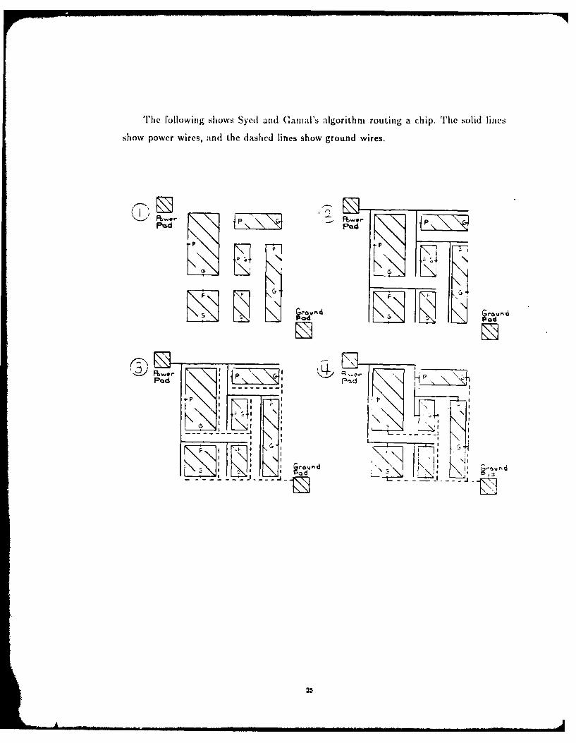
'I'hc following shows Syed and C'nial's algorithni routing a chip. The solid lilies
show power wires, and the dashed lines show ground wires.
__. , . Power
GG
k rowP Gr,.-
Pe~w~P
G'
25
4.2. Iothermel ad Mlynviki's algorthl 1IM8I]
Rothermel and Mlynski's algorithin divides the chip into left and right halves,
routes the VDD connection points that are in the left half, routes the GND connection
points that are in the right half, and then completes the trees. This algorithm's use of
a vertical line to divide the chip iuto regions so that a tree can grow separately in each
region is similar to Section 6.3's algorithm's use of a Ilamiltonian cycle.
This algorithm assumes that there is one VDi) pad in the chip's left half arnd one
GND pad in the chip's right half.
The algorithm first uses a vertical line to divide the chip into halves. A line-search
algorithm similar to lightower's routes one tree that connects the VDD pad to all
the VDD connection points in the left half and another tree that connects the GND
pad to all the GND connection points. An algorithm similar to Lee's completes the
trees. Then, tree traversal calculates each branch's required width. The algorithm
then appropriately widens the wires. If necessary, the algorithm adjusts the modules'
placement to accommodate the thicker wires.
4.3. Lhota's algorithm [1,1IO80]
To obtain insight on the best way to lay power and ground wires, Frank J. Lhota
studies the problem in graph theory of finding two trees that span a set of vertices
in the Cartesian plane, that lie in the plane, and that do not intersect each other.
An optimal solution to this problem is one in which the two trees' combined length is
minimum.
One method of solving this problem is to find a minimum spanning tree and then
find the shortest tree that spans the vertices but does not cross the first tree. This
method is similar to Section 6.1's algorithm.
Lhota's first result is a lower bound on the combined length or the trees in the
optimal solution. Each of the optimal solution's two trees spans the vertices. As such,
the length of each is at least a minimum spanning tree's. Thus, the optimal solution's
trees' combined length is at least twice a minimum spanning tree's.
26
Now consider the technique or finding the trees by first finding a minimurn spanning
tree and then finding another spanning tree that does not cross the first. It sometimes
happens that a certain minimum spanning tree forces the second tree to have twice the
length of the minimum spanning tree. This solution's trees' combined length is then
three times a miniuium spanning tree's.
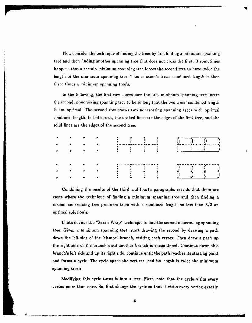
In the following, the first row shows how the first minimum spanning tree forces
the second, noncrossing spanning tree to be so long that the two trees' combined length
is not optimal. The second row shows two noncrossing spanning trees with optimal
combined length. In both rows, the dashed lines are the edges of the first tree, and the
solid lines are the edges of the second tree.
second t p- -- 2 a*I I I I
I I I II
* aP a1 a---------------------------------------.---a"-- I
t I I I I
, i I I,
Combining the results of the third and fourth paragraphs reveals that there are
cases where the technique of finding a minimum spanning tree arnd then finding a
second noncrossing tree produces trees with a combined length no less than 3/2 an
optimal solution's.
Lhota devises the "Saran-Wrap" technique to find the second noncrossing spanning
tree. Given a minimum spanning tree, start drawing the second by drawing a path
down the left side of the leftmost branch, visiting each vertex. Then draw a path up
the right side of the branch until another branch is encountered. Continue down this
branch's left side and up its right side. continue until the path reaches its starting point
and forms a cycle. The cycle spans the vertices, and its length is twice the minimum
spanning tree's.
Modifying this cycle turns it into a tree. First, note that the cycle visits every
vertex more than once. So, first change the cycle so that it visits every vertex exactly
27
once. Deleting one edge from the resulting cycle produces a path that visits every
vertex exactly once. This path is a noncrossing spanning tree with length twice the
minimum spanning tree's. Call this second tree the Saran- Wrap tree.
Note how this Saran-Wrap tree differs from Section 6.1's second, noncrossing tree.
The Saran-Wrap tree is a spanning tree whereas Section 6.1's tree is a Steiner tree. In
general, Steiner trees are shorter. Therefore, the following results cannot be directly
applied to determine Section 6.1's trees' length.
The solution containing a minimum spanning tree and a Saran-Wrap tree has a
combined length three times the minimum spanning tree's. This length is within 3/2
of optimal.
Since the shortest noncrossing tree's length must be less than or equal to the
Saran-Wrap tree's, the solution containing a minimum spanning tree and the shortest
noncrossing spanning tree is also within 3/2 of optimal. However, a previous result
indicated that there are cases where this solution is no better than 3/2 of optimal.
Thus, in some cases the Saran-Wrap tree's length is very close to the shortest
noncrossing tree's. However, there are cases where the Saran-Wrap tree's length is twice
that of the shortest noncrossing tree.
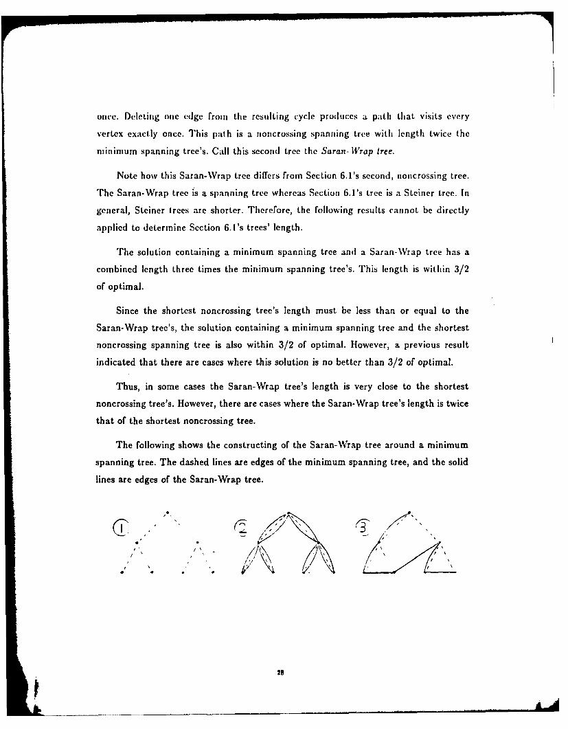
The following shows the constructing of the Saran-Wrap tree around a minimum
spanning tree. The dashed lines are edges of the minimum spanning tree, and the solid
lines are edges of the Saran-Wrap tree.
KL. //,,
, '
/ I, 111
5. 1i1i ! SYSTEM
5. 1. Overview of' the III System
The l'lac'eient-lnterconnect (!l1) Research Group under Prof. Ronald Iivest at
Massachusetts Institute of Technology is implhementing iII l]Sl ;In) al1 ted design
svstei for custom, single-liver metal, NMOS and CMOS chips. The PI group is taking
an ;algorithiiic approach to the problem or COmijplt'ely aitomtiat ing the placetment and
interconnect phases of chip desigl. This group's goal is tile create a system that
produces high-quality output with a in iinium amount of human interaction. Prof.
Rivest described this sy tern, called PI, at the 19th DAC Conference ([RI821).
The following are two important aspects of how PI views the chip design problem:
" In dealing with chip objects, PI uses the absolute coordinates of their
locations on the chip instead of describing their positions symbolically or
relative to other chip objects.
* PI regards modules as rectangles with connection points to connect to
wires outside the module. Since P1 does not know the wiring internal to
the module, it never lays a wire over a module.
When PI routes a chip, it divides the placement-interconnect design process into
four phases:
* Placing tile modules on the chip.
* Routing the power and ground nets.
* Routing the signal nets.
* Compacting the chip regions to reduce the chip's size.
Pl subdivides the third phase (signal routing) into four subphases:
A2
* I)iuing the cha nnels.
* Routing the nets globally.
i )eciding where the wires should cross the channel edges.
* Routing the channels.
The rest of' this chapter on N! describes each phase and subphase with comments
on how eact relates to the power-ground algorithms.
5.2. Placing the modiles on the chip
The placement phase puts each rectangular module into a specific location on the
chip. Upon input, P knows each module's dimensions and the locations of its connection
points. After placement, each module has an exact, absolute location. Placement has
two subphases: one places the pads, which are the modules that carry communications
to and from the chip; the other places the logic modules, which are the modules that
perform the desired logical or functional operations.
5.2.1. Placing the pads
PI places pads (power pad(s), ground pad(s), and signal pads) along the chip's
perimeter. The goals are to place the pads on as few sides as possible and to orient each
pad so its user-specified outside edge is closest to the chip's edge. This pattern of lining
up pads along the chip's perimeter was a major reason for arranging the power-ground
wires in rings, described in Section 6.4.
5.2.2. Placing the logic modules
When PI places the logic modules, it first goes through a top-down, min-cut
procedure to determine the approximate "cations of each one, then goes through a
bottom-up, successive-pairing procedure to determine each module's orientation and
exact location.
At each step, the min-cut procedure uses a line to divide the modules into two
groups so that many of the wires connecting the signal nets' connection points will lie
30
with in each group and Few will lie between groups. lii hir.. step, the lie ivhides
the chip into two regions. The 11in-c'ut proc'cdure pis soine iiodhils oil either side of
the lite. Subject to balancing counstr;iitts that enstre all modules will not lie on one
side, the goal is to uiinilize the number of signal wires that will cross (he line. To
divide the chip into regions, the procedure uses either a vertical or a horizontal line,
depending on which provides the minimum cut.
The procedure continues in a binary, (op-down aiitmer. EI.th region is divided
into two by either a vertical or horizontal line. loving nlodules within each region
liniunizes the number of wires that cross each line. This process continues until each
module is in its own region.
Then tile bottom-up procedure considers two adjacent regions, each containing
one module, to determine for each module its orientation and its placement relative to
the other module. Each module has eight possible orientations, produced by rotating
it 90 degrees four times, flipping it, and rotating it four more times. The definition of
one module's placement relative to another is the differences between the x-coordinates
of the modules' left sides and between the y-coordinates of their bottom sides. In the
next two paragraphs, placement refers to both the orientation and relative placement
of a module.
The bottom-up procedure chooses the best placement for the two modules. When
choosing, the procedure has as its goal minimizing the area of the final layout of wires
and modules. At this point, the procedure has to estimate how much room the signal
routing will require. After it finds the best placement, the two regions become one.
Within the new region, the modules' placements are fixed.
The procedure continues in a bottom-up, successive-pairing manner. When every
region has a pair of modules, the procedure considers the best placement for an adjacent
pair of regions and merges this pair into a new region. This process continues until all
the logic modules are in one region. At this point, each module's location becomes its
exact, absolute location.
31
5.3. Rou ting the power and gromid nets
This phase uses the adgorithms described more fully in Section 6.4 arid Chapter 7.
These algorithms lay a ground ring and a power ring to connect the pads, lay a ground
tree and a forest of power trces to connect the logic modules, and use the resizer to
widen each wire to its appropriate width.
5.4. Routing the signal nets
Signal routing's goal is, for each signal net, to lay a tree of %%ires that span the
signal net's connection points. The following sections describe each of signal routing's
subphases.
5.4.1. Defining the channels
Channel definition divides the chip area into nonoverlapping rectangular chip
objects. Each object is one of the following:
" a module
* a free channel-a routing region that conatins no wires or modules
* a covered channel -a routing region with a power or ground wire occupying
the region's entire metal layer but nothing on the other layers
The channel definition algorithm is executed during many stages in the PI system.
For example, it may be executed immediately after placement, before power-ground
routing is done. Since at this stage there are no power or ground wires, the algorithm
divides the chip into modules and free channels. On the other hand, executing the
algorithm after the power-ground routing is completed divides the chip into modules,
free channels, and covered channels.
Channel definition draws lines on the chip until every chip region is a rectangle.
A line separating two channels is a channel edge. In choosing among possible sizes and
shapes for the channel layout, channel definition's goal is to minimize the total length
of the channel edges it must draw to form the channels.
32
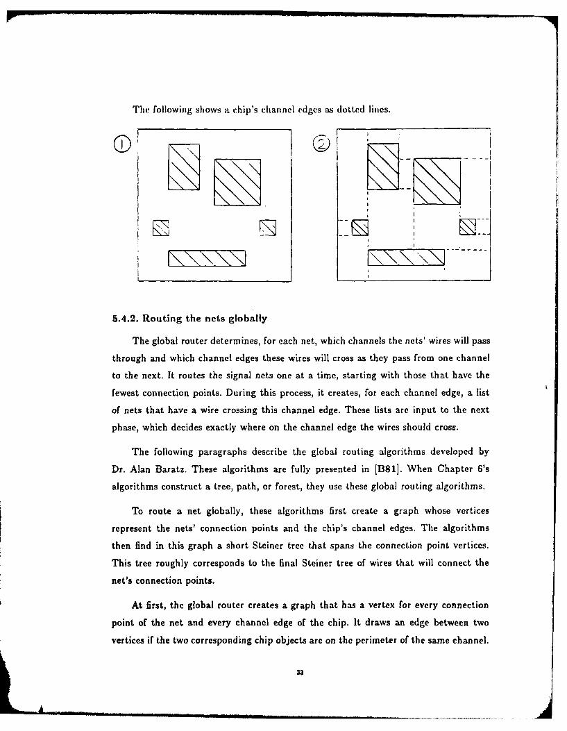
[rhe following shows a c hip's channel edges as dotted lines.
5.4.2. Routing the nets globally
The global router determines, for cach net, which channels the nets' wires will pass
through and which channel edges these wires will cross as they pass from one channel
to the next. It routes the signal nets one at a time, starting with those that have the
fewest connection points. During this process, it creates, for each channel edge, a list
of nets that have a wire crossing this channel edge. These lists are input to the next
phase, which decides exactly where on the channel edge the wires should cross.
The following paragraphs describe the global routing algorithms developed by
Dr. Alan Baratz. These algorithms are fully presented in [1381]. When Chapter 6's
algorithms construct a tree, path, or forest, they use these global routing algorithms.
To route a net globally, these algorithms first Create a graph whose vertices
represent the nets' connection points and the chip's channel edges. The algorithms
then find in this graph a short Steiner tree that spans the connection point vertices.
This tree roughly corresponds to the final Steiner tree of wires that will connect the
net's connection points.
At first, the global router creates a graph that has a vertex for every connection
point of the net and every channel edge of the chip. It draws an edge between two
vertices if the two corresponding chip objects are on the perimeter of the same channel.
33
Each edge's cost rellects how far one chip object is froii the other, how crowded tle
coiimoji channel is because of other nets that have already been routed through it,
and whethaer it is a free or covered channel.
After creating the graph, the algorithnis grow paths from the connection point
vertices until the paths meet to formn a tree. If there are ?i connection point vertices,
there are initially n basis groups, each consisting or one connection point vertex. Paths
grow si iult-aneously in all dIirections froii all hasis groups. Eventui ally, two paths meet,
forming a bridge between two basis groups. The vertices along this bridge are two
connection point vertices plus a number initerinediate vertices representing channel
edges. Then a new basis group consisting of all the vertices on the bridge replaces the
two old ones. In the next step, paths grow from the n - 1 basis groups. This process
repeats until there is just one basis group. At this point, reconstructing each bridge
that connected two basis groups builds a Steiner tree that connects the n connection
point vertices.
The method of growing the paths ensures the process results in a short Steiner
tree. To see why the tree is short, consider how the algorithms grow the bridge that
connects two basis groups. They grow the shortest bridge because they grow the path
from each basis group by adding the shortest edges first, as in Dijkstra's algorithm. To
see why the final tree is a Steiner tree, consider the branch points that can occur at
channel edge vertices. Paths grow simultaneously from each vertex in the basis group,
channel edge vertices as well as connection point vertices. The path from a channel
edge vertex may be the first to meet a path from another basis group. The final tree
will then have a branch point at this channel edge vertex. Since this channel edge
vertex is not one of the original vertices to be spanned by the tree, this branch point
is a Steiner point.
5.4.3. A power-ground modification of global routing
When determining the cost of each edge in the original graph, the global router
considers whether the edge crosses a free or a covered channel. If it crosses a covered
channel, the global router increases the edge's cost to reflect the disadvantages of
running a signal wire over the metal wire that creates the covered channel.
34
Imposing a high penalty oil edges that cross covered channels ensures such edge
will never appear in the final Steiner tree. The power-ground phase uses this technique
to construct noncrossing trees of inetal wires. Arter connecting the logic modules with a
ground tree of metal wires, the power-ground algorithins call channel definition, which
turns the metal wires into covered channels. They then construct a forest of power
trees to connect tlie logic modules. A high penalty at this point preveints these power
trees from crossing the metal wires of the previously laid ground tree.
5.4.4. D~eridin|g where the wires should cross the channel edge
The crossing placement phase determines where the signal wires cross the channel
edge. At the end of the global routing phase, cach channel edge vertex has a list of
signal nets. A signal net appears on a vertex's list if that vertex appears in the Steiner
tree that routes the signal net. Thus, a vertex's list indicates which signal wires will
cross the channel edge that corresponds to the vertex. Using such information as where
the wire comes from and where it is going, crossing placement assigns to each wire a
crossing location.
5.4.5. Routing the channels
The channel router determines exactly where the wires run in each channel. At
this point, crossing placement has already determined the exact location where a wire
enters and exits the channel. The channel router lays wires to connect each entry point
with its exit point. Because the entry and exit points are fixed, the channel router can
attack each channel as a separate, independent, self-contained routing problem.
PI has three channel routers. The channel routing phase first calls the simplest
router, which handles many common layouts. If this router cannot find a valid routing,
the second router searches for a routing by dividing the channel into slices. If the
second router fails, the third router searches for a routing by using Lee's algorithm.
35
5.5. l e'siziiig Lhe chip regions to reduce the clhip's size
The resizer modifies the placenelnt of \w'ires and modules to accolm)lishi any of
three tasks:
" Widen power-ground wires.
* Provide more room for signal routing.
" Compact a complete layout of imodules id wires.
The resizer modifies placement once in the x direction and then once in the y
direction. The next two paragraphs describe resizing in the x direction. A similar
process resizes in the y direction.
First, the resizer creates a graph. Each vertex of the graph corresponds to a
vertical side of a chip object, such as the vertical side of a wire or module. Between
two vertices, the resizer creates a constraint, which is either a minimuum or an equality
constraint. For instance, the constraint between a module's left and right sides is an
equality constraint because the module's dimensions are fixed. On the other hand, the
constraint between a channel's left and right sides is a minimum constraint because a
channel can be wider than its required width.
Once the graph is complete, the resizer finds the longest path from the vertex that
represents the chip's left side to the vertex that represents the chip's right side. The
resizer uses information about this path to find an x-coordinate for each vertex in the
graph so that all constraints are satisfied. Then, for each vertex and its x-coordinate,
the resizer moves the chip objects so the corresponding vertical side is located at the
x-coordinate. This completes resizing in the x-direction.
The next three paragraphs describe how the resizer is used by the power-ground
phase, the signal-routing phase, and the compaction phase.
The power-ground phase uses the resizer to widen the power-ground wires. A
tree-traversal algorithm, described in Chapter 7, finds how much current flows through
£ 36
each po wer-ground wire. Ile iainoit of current determines emdh wire's riiiinium
width. The power-ground phase, for each wire, calls the resizer, indicating the wire's
left and right sides aid its mininium width constraint. lResizing produces wires of the
appropriate width.
Ihe signal-routing phase calls the resizer either in its crossing placement subphase
or it channel routing suil )ase. Crossing placement uses the resizer to lengthen cinel
edges. After glolal routing, crossinig pliceirent may filt 1hat a channel edge is not
wide enough to ;ccommo(Laoe all the wires that must cross it. Crossing placement calls
the resizer, indicating the channel's endpoints and the length required by the crossings.
The channel router uses the resizer to give it more room for routing. If, at first, the
channel router fails because the channel is too small, it calls (he resizer, indicating the
channel's left and right edges, to increase the width of the channel.
After the channel router succeeds, the reduction phase uses the resizer to compact
the layout. Given a layout of wires and modules, the resizer collects constraints that
ensure the layout satisfies the design rules. Subject to the constraints, the resizer
reduces the size of the chip as much as possible.
37
6. FOURALGORITIIJMICMIETi IODSTO GIROV NONCROSSING
TrREES
This chapter describes four new methods to construct the power and ground trees
and discusses each one's advantages and disadvantages. As for running efliciently and
producing high-quality results, the fourth method is the best. The imiplementation of
this fourth method forms part of P1's power-ground phase. The four methods are:
* Constructing the trees sequentially, one after the other.
* Constructing the trees concurrently, one branch at a time.
* Drawing a lamiltonian cycle through the modules, then constructing the
trees, respecting the boundary defined by the cycle.
* Laying two rings to connect the pads, then constructing the trees
sequentially to connect the logic modules.
The algorithms use Section 5.4.2's signal-routing algorithm or Section 5.4.3's
modified signal-routing algorithm to construct Steiner trees to connect various sets of
points. In discussing running times of the algorithms, ST(V) is the time each algorithm
takes to route V vertices.
6.1. Constructing the trees sequentially, one after the other
This algorithm constructs one tree and then constructs the second tree so that
it does not cross the first. To construct the first tree, Section 5.4.2's signal-routing
algorithm finds a short Steiner tree that connects the first net's connection points. To
construct the second tree, Section 5.4.3's modified signal-routing algorithm constructs
a short Steiner tree that connects the second net's connection points and that does not
cross any wire of the first tree.
The advantage of this algorithm is that it quickly produces a valid power-ground
layout in time O(2ST(V)). The layout is valid because one tree connects all the first
3R
net's connection p~oint~s, the othe~r tree coiinects all the second net's connection points,
and the trecs do not cross each other.
The disadvantage of this algorithm is that the trees' comibined length may not be
near optimal. The first trec's length is near the optimal for a spanning Steiner tree.
However, when routing the second tree, the facts that the first is already complete and
that the wires of the second cannot cross those or the first often require the second tree
to have long branches. According to the result in Section 4.3, paragraph 5, there are
cases where constructing the trees sequentially produces trees with a combined length
at least 3/2 of optimal. It should be noted, howver, that the result in Section 4.3,
paragraph 9, indicates that, for most cases, with effective algorithms to grow Steiner
trees, the trees' length wvill be within 3/2 of optimal.
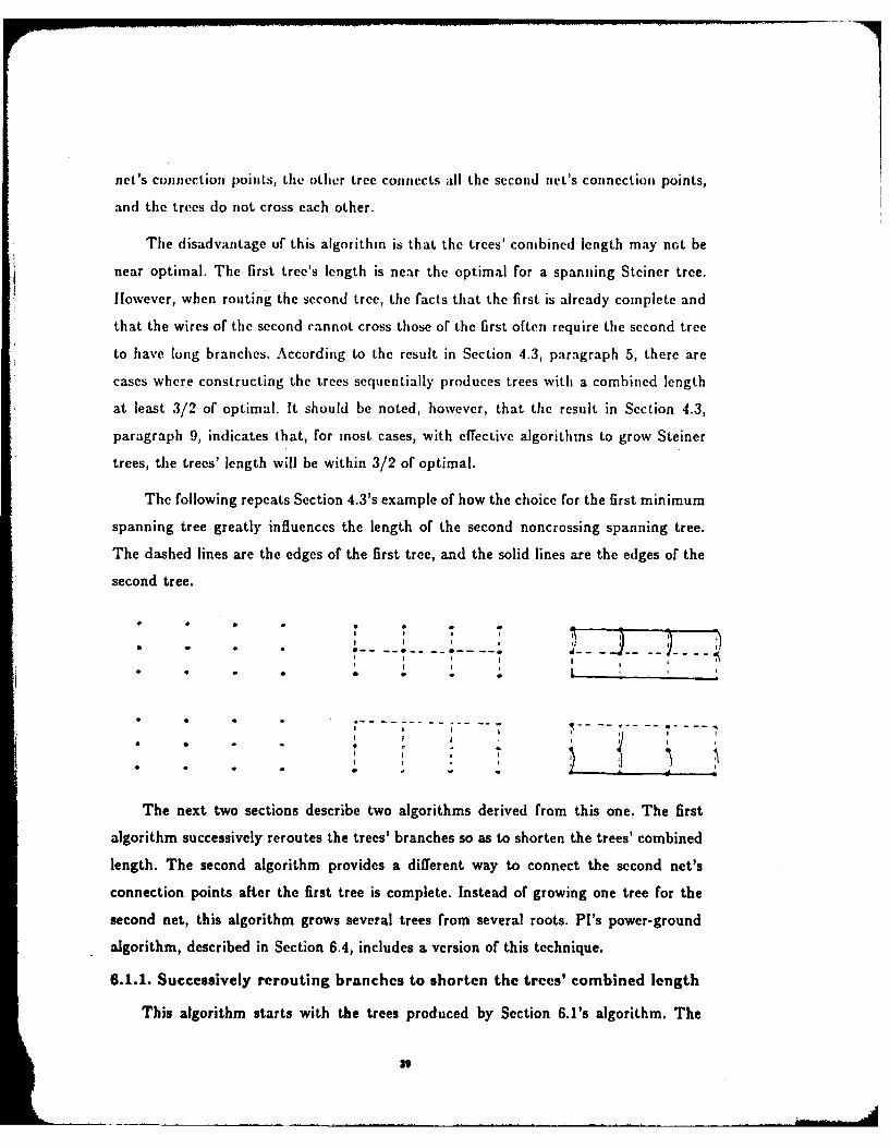
The following repeats Section 4.3's example of how the choice for the first minimum
spanning tree greatly influences the length of the second noncrossing spanning tree.
The dashed lines are the edges of the first tree, and the solid lines are the edges of the
second tree.
legh Th seon aloih poie a difeen wa ocnettescn e'
concto ponsatrtefrtte scmlte nta fgoigoete oh
Theon net twsetosdcrbtw algorithmgrwseratesfomsderveda fromts this oerTegrstn
algorithm, described in Section 6.4, includes a version of this technique.
6.1.1. Successively rerouting branches to shorten thc trees' combined length
This algorithm starts with the trees produced by Section 6.1's algorithm. The
31
dis.advantage, of' th'se I rves is that tIe I re' is very short wlireas Ili' t)thvr Itcind to be'
very long. lh algorthnm ds'ctrib,'d in this section sh(ortvis (lie eto'C nlnd %%lhl slihlly
lngthlingl (lit' first. This retut'es th' tre'es' tcomibiiedl length.
The second tret' mulay b' longer than ie'tssary h ,(auise it iay hiav' lnig, hraui(lehss
paths. hi gtiieral, short trees are v'ry bushy, with fre 'juit braicihinig. hlit ordr to
(ouitu'ct a few (t)uuIt'tionl points to the rest of* the st.,id tret,, I lre is often a
lbr:tuhhil.ss path Ihat gots arouid an obstrietiig l)rach (if' t liv first tree. ''liis path
grt'ati)y increases the sectond t ret's length.
The alIgoritim shortens (t secoid tree by deletiig that trt'e's lo)igt-st hraiciless
path and then (ouilt'eting the resulting ('tco)miniiUt.,, of tlh trtete. l)et tug lht path Iav, s
two coniected Colipolents. Ignoring the first tree, the algorithi finds the shortest path
that connects these components. Because the algorithm ignored the first tree, this path
probably crosses wires of the first tree. The algorithm then deletes any wire of the first
tree that the new path crosses. Because of this, the first tree has now become several
connected components. The algorithm finds paths that connect these components and
that do not cross the wires of the second tree. The result is two complete, connected
trees.
40
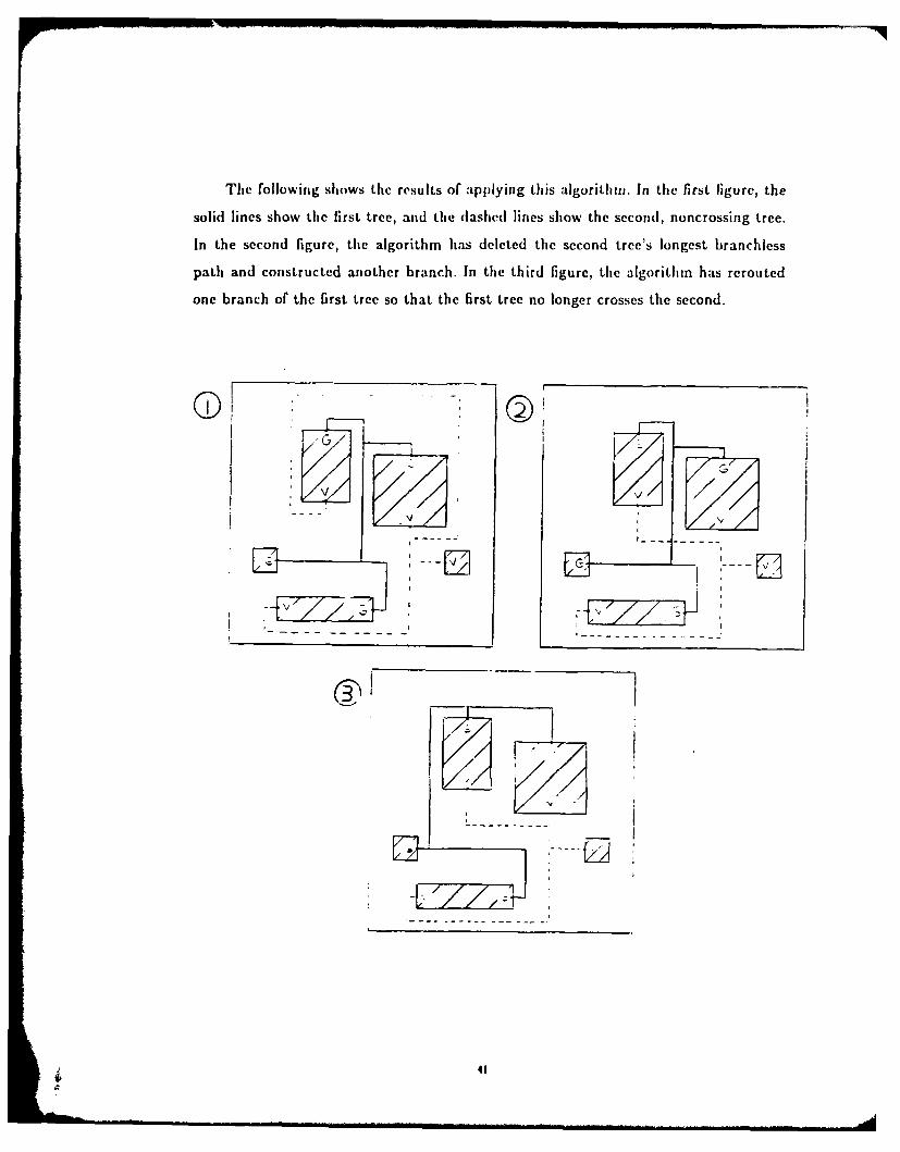
The following shows tle results of applying this algorithm. In tile first figure, the
solid lines show the first tree, and tile dashed lines show the second, noncrossing tree.
In the second figure, the algorithm has deleted the second tree's longest branchless
path and constructed another branch. In the third figure, the algorithm has rerouted
one branch of the first tree so that the first tree no longer crosses the second.
* 'I,
- .V ;I
I . . . . . . . .. . .
I14'
At tiils point, the algorithmi compares the new trees' combined Ih nglh with the
original trees'. If the length decreased, as in the above example, tie new trees become
the best layout yet found. If not, the original trees remain the best layout yet found,
and the algorithi marks the longest branclhless path to tell future iterations that
deleting this path will not lead to shorter trees.
The algorithm continues by searching in the best layout yet found for the longest
)ranchless path not yet considhered. These iterations continue until the algorithm has
considered every branlchless path in the current second tree without reducing the trees'
combined length. At this point, dhe trees of the current layout becone tihe linal power
and ground trees.
The advantage of this algorithmu is that at each step the layout is a valid power tree
and ground tree and that at the end of each step the trees' combined length is never
greater than it was at the end of the previous step. This gives the user flexibility. One
user may tolerate a large combined length for the trees but require a short computation
time. This user should run the algorithm through just a few iterations. Another may
tolerate a long computation time but require a short combined length for the trees.
This user should run the algorithm to completion.
The disadvantage of this algorithm is that running it to completion requires a long
computation time. This is due to the large number of branchless paths to be considered
for deletion and the extensive rerouting required after deleting each branchless path.
6.1.2. Constructing one tree, then a forest of trees
This algorithm grows the first tree in the same way Section 6.1's algorithm does.
To connect the second net's connection points, this algorithm grows several trees.
This technique makes it more likely that the second tree will be short. Constructing
the second tree is difficult because the wires have to avoid crossing the first tree.
Constructing several trees makes it less likely that a long, branchless path will be
needed to get around a branch of the first tree. For example, the algorithm could place
one root for the second tree between the tips or two main branches of the first tree. A
42
tree construc'ted from this root could connect the second net's connection points, that
lie between those branches without worrying about crossing the branches.
The advantage of this algorithm is that. growing the small trees requires less
computation time and results in trees of smaller total length than growing one large
tree.
The disad vantage of this algorithii is th at only special layouts allow one of the
trees to have multiple roots. Il's power-ground phase uses this algorillin to grow the
Vl)I) tree for the logic modules. Since a VI) ring surrounds the logic modules, as
described in Section 6.4.1, the power-ground phase can pick points along this ring as
the VDD trees' roots. These roots and the trees that grow front thetn are connected to
the VDD pad through the VDI) ring.
6.2. Constructinig the trees concurrently, one branch at a time
This algorithm constructs the two trees concurrently, one branch at a time. At
each step, the algorithm constructs the branch that will least hinder the other tree's
growth.
The trees' edges are of two kinds:
* tentative edges that indicate the tree's probable future growth
• committed edges that will definitely appear in the final layout
No edge, tentative or committed, can cross a committed edge. One tentative edge can
cross another.
The algorithm begins by laying two complete trees of tentative edges. For each
tree, the algorithm finds a short Steiner tree that spans the connection points. Since
all the edges are tentatative edges, crossings are allowed, and the algorithm can grow
each tree without considering the other.
The algorithm then determines which tentative edge should turn into a committed
edge. To do this, it observes, for each tentative edge, the changes that would occur
if the edge became a committed edge. Suppose that the algorithm is considering a
43
telitative edge il the first tree that a teintative edge ill the seC'trd tree crosses. Tiing
the first tree's tentative edge into a comlmitted edge voUhil r'pItire some rerouiling of the
second tree's tentative part to avoid crossing the new committed edge. The algorithm
notes how much longer tle new second tree is haln the former.
After considering all the trees' tentative edges, the algorithm c'hanges some
tentative edge into a committed edge such that this change produtces the least increase
in tle length of tle opposite tentative tree. After c ,angi,,g the tentative edge to a
commniitted edge, the algorithm appropriately redraws the opposite tentative tree.
Considering the current layout of trees, the algorithm again searches for the best
tentative edge to change into a committed edge. This continues until there arc no more
tentative edges. At this point, the two trees of committed edges are the final power
and ground trees.
44
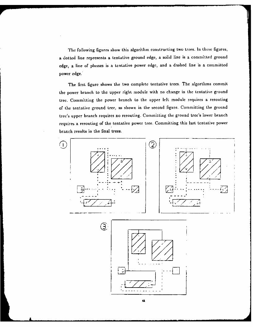
The following figures show this algorithm constructing two trees. In these figures,
a dotted line represents a tentative ground edge, a solid line is a committed ground
edge, a line of plusses is a tentative power edge, and a dashed line is a committed
power edge.
The first figure shows the two complete tentative trees. The algorthins commit
the power branch to the upper right module with no change in the tentative ground
tree. Committing the power branch to the upper left module requires a rerouting
of the tentative ground tree, as shown in the second figure. Committing the ground
tree's upper branch requires no rcrouting. Committing the ground tree's lower branch
requires a rerouting of the tentative power tree. Committing this last tentative power
branch results in the final trees.
O 0.
* __
/
-43 -
. 45
The advantage of this algoritin is that it provides a baLhIMCd, SY111n1Vtric approach
to constructing the trees. This contrasts with the algoritli described in Section 6.1,
which from the beginning gives the advantage to the lirst tree.
The disadvantage of this algorithm is that it requires a long computation time.
This is due to the large number of tentative edges it must consider and, for each
tentative edge consilered, the extensive rerouting of the op~posite tentative tree that
must he carried out. IHowever, there are several characteristics of tlie algorithim that
keep the running time reasonable.
During the algorithm's first steps, there are many tentative edges near the trees'
roots that tentative edges of the opposite tree do not cross. Since no edge crosses them,
turning these tentative edges into committed edges will not increase the length of the
opposite tentative tree. Thus, the first steps require little computation time.
During the algorithm's last steps, most of the trees' edges are committed edges.
Reconstructing the trees' tentative parts is quick because the tentative parts are so
small. Thus, the final steps require little computation time.
6.3. Drawing a lamiltonian cycle through the modules, then constructing
the trees, respecting the boundary defined by the cycle
This technique of keeping the power and ground trees from crossing was presented
at the 20th DAC Conference ([MO83]).
6.3.1. Using the llamiltonian cycle to divide the chip into regions
A Harniltonian cycle helps construct noncrossing trees because it divides the chip
into two regions-one outside and one inside the cycle. If the cycle has all one net's
connection points inside and all the other's outside, the cycle divides the chip into a
VDD region and a GND region. The tree that connects each net's connection points
lies within that net's region. Since the regions are separate, the trees do not cross.
For a set of modules, there are many Hamiltonian cycles, and each relates to a
different power-ground layout. To see this relationship, consider a chip with the power
and ground trees already laid. Imagine standing on a module with its VDI) connection
46
points to your right aind its CNI) connection points to your left. When you try to
walk to another module, keeping the Vl)I) wires on your right and the (N) wires on
your left will determine the next module you encounter. Continuing the walk takes you
through every module and back to where you started. Thus, a layout of power and
ground trees determines a llamilionian cycle through the modules.
Using the reverse of the above technique, drawing the Ilamiltonian cycle first
determines the layout of power and ground trees. In deciding which IHamiltonian cycle
to draw, the algoritlim should pick the cycle that will produce the shortest. power and
ground trees. It is therefore instructive to consider how a cycle's characteristics relate
to the corresponding layout's characteristics.
Such a consideration shows that the desired Hlamiltonian cycle is the shortest one
that can be found in a reasonable amount of time. One support for this conclusion
arises from the need for the Ilamiltonian cycle to split the chip into two regions. To
produce two regions, the cycle must not cross itself. The shortest cycle does not cross
itself, and, in general, shorter cycles have fewer crossings. This indicates a short cycle
is desirable. Another support for this conclusion is that shorter cycles produce regions
of simpler shape. Routing in such regions produces simpler, shorter, more regular trees.
6.3.2. Defining distance from one module to another
This section defines the distance from one module to another. The calculation of
the cycle's length uses this distance, which is basically the Manhattan distance between
the modules.
In keeping with the notion of walking along the cycle, a module's OUT point is
defined to be the point where the cycle leaves the module. As it leaves the module, the
VDD connection points are to its right, the GND connection points to the left. To make
this more specific, find the most counterclockwise VDD connection point and the most
clockwise GND connection point. The module's OUT point is on the module's perimeter
halfway between these two connection points. The OUT point is counterclockwise from
the VDD connection point and clockwise from the GND connection point.
47
A mlodule's IN point is defined to bc the point where the cycle cnltcrs thw muduidw. To
locate it, find the most clockwise V)D connect ion point and the most co unterclock wise
GND connection point. The IN point is halfway between them, clockwise from the
VDD connection point, counterclockwise from the UNI) connection point.
The Manhattan distance from (z , Y I) to (X,',Y2) is IT2 -X I + IY2 -Y I"
The distance from Module A to Module 13 is defined to be the Manhattan distance
fron A's OUT point to I's IN point. Note that this delinition of distance is not
symmetric.
6.3.3. Finding a short llamiltonian cycle
This section describes an algorithm that finds a short lamiltonian cycle. This cycle
consists of abstract edges, each edge having a module at each end. An edge indicates
that the cycle goes from one module to the other but does not specify exactly where
the cycle runs.
It is convenient to think of a lamiltonian cycle as an ordering of the modules. If
the modules are MI, M 2, M 3, ... , M,, any ordering (AM, M 2 MiA,3 ... , Mi.) designates
a lamiltonian cycle with abstract edges (Mi, Mi9) M 2 1 Mi 3), , (Mi.,, Mil).
4'
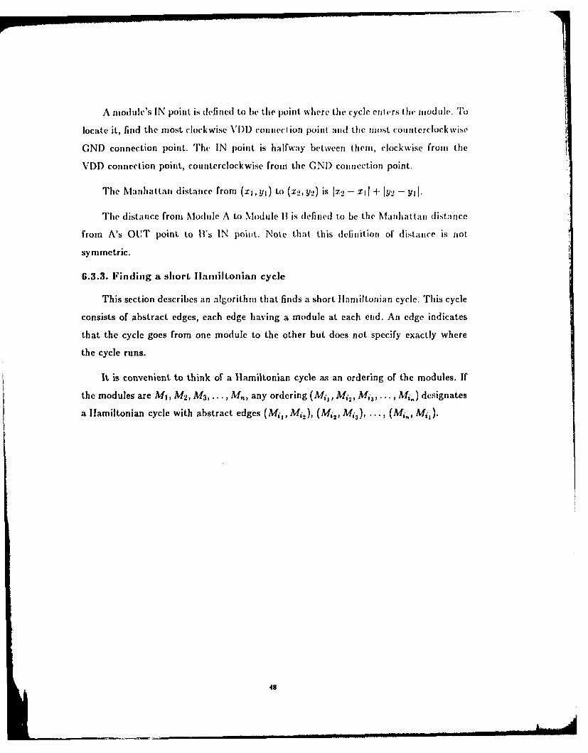
A module's IN point is defined to be the point wliere the cycle enters the module. To
locate it, find the most clockwise \1)!) connect ion point and the most counterclock wise
GND connection point. The IN point is halfway between theni, clockwise from the
VDD connection point, counterclockwise from the GNI) connection point.
The Manhattan distance from (X1 , YI) to (z, Y2) is I2' - X1I + IY2 - YII.
The distance from Modulc A to Module 13 is defined to be the Manhattan distance
from A's OUT point to 11's IN poinit. Note that this definition of distance is not
symmetric.
6.3.3. Finding a short Ilaniitonian cycle
This section describes an algorithm that finds a short lamiltonian cycle. This cycle
consists of abstract edges, each edge having a module at each end. An edge indicates
that the cycle goes from one module to the other but does not specify exactly where
the cycle runs.
It is convenient to think of a Hamiltonian cycle as an ordering of the modules. If
the modules are MI, M2 , M3 ,..., M,,, any ordering (Mi, Mi2, Mi3,... , Mi.,) designates
a lamiltonian cycle with abstract edges (Mi,, Mi2 ), (M i, .. J),..., (Mi, Mi).
4'
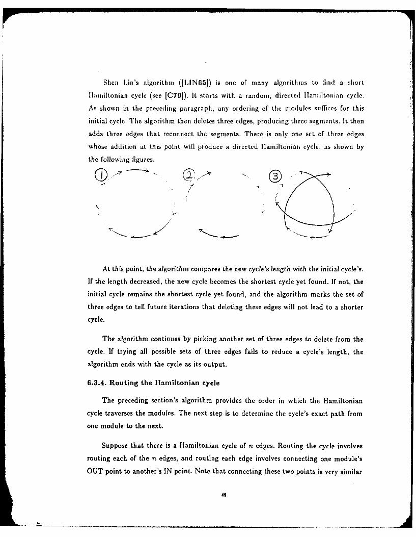
Shen Lin's algorithm ([LING5]) is one or many algorithms to find a short
llantiltonian cycle (see [C79]). It starts with a random, directed Iamiltonian cycle.
As shown in the preceding paragraph, any ordering of the modules suffices for this
initial cycle. The algorithm then deletes three edges, producing three segments. It then
adds three edges that reconnect the segments. There is only one set of three edges
whose addition at this point will produce a directed lamiltonian cycle, as shown by
the following figures.
1 -
//
At this point, the algorithm compares the new cycle's length with the initial cycle's.
If the length decreased, the new cycle becomes the shortest cycle yet found. If not, the
initial cycle remains the shortest cycle yet found, and the algorithm marks the set of
three edges to tell future iterations that deleting these edges will not lead to a shorter
cycle.
The algorithm continues by picking another set of three edges to delete from the
cycle. If trying all possible sets of three edges fails to reduce a cycle's length, the
algorithm ends with the cycle as its output.
6.3.4. Routing the Ilamiltonian cycle
The preceding section's algorithm provides the order in which the Hamiltonian
cycle traverses the modules. The next step is to determine the cycle's exact path from
one module to the next.
Suppose that there is a Hamiltonian cycle of n edges. Routing the cycle involves
routing each of the n edges, and routing each edge involves connecting one module's
OUT point to another's IN point. Note that connecting these two points is very similar
4,
to routing a signal net that has two connection points. For this reason, the algorithims
of Section 5.4 can route each edge of the lamiltonian cycle.
Specifically, using Section 5.4.3's modified algorithm to route the edges ensures
that the cycle will not cross itself. The algorithm routes one edge at a time. When
routing an edge, the algorithm ensures that ils path does not cross a previously routed
edge's path.
The order in which the algorithim should route the nets is not obvious. Because
one edge's path cannot cross another, a different order for routing could produce quite
different paths for the cycle.
The following example shows how the order of routing the edges affects the final
layout of the cycle. The Hiamiltonian cycle goes from Module 1 to Module 2 to Module
3. The second figure shows the result of routing the edges in the following order:
Module 2 to Module 3, Module 3 to Module 1, and Module 1 to Module 2. The third
figure shows the result of the following routing order: Module 1 to Module 2, Module
3 to Module 1, and Module 2 to Module 3.
50
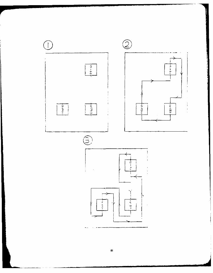
0 __
I
0
N;IW .9
51
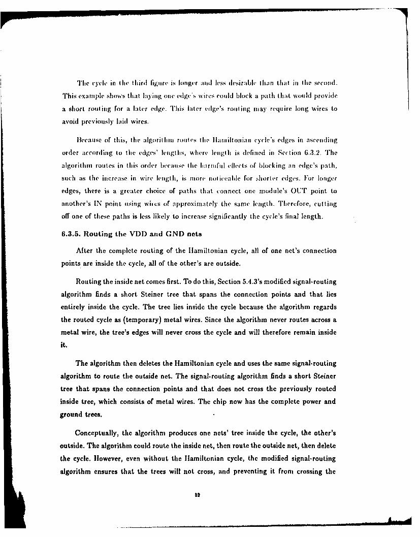
The cy Iv in Ihe third figure is loniger and less des-irable dial that il the second.
This example shows thai laying one edge's irles could block a path that would provide
a short routing for a later edge. This later edge's routing may require long wires to
avoid previously lhid wires.
lBecause or this, the algoriIim roule Iie II: miltonian cycle's edges in ascending
order according to the edges' lengths, where leugth is defined in Section 6.3.2. The
algorithmm routes in this order l eca. se (lie ha rmiful mellects of blocking an edge's path,
such as the increase in wire length, is more noticeable for shor er edges. For longer
edges, there is a greater choice of paths that connect one module's OUT point to
another's IN point using wires of approximnately the same length. Therefore, cutting
off one of these paths is less likely to increase significantly the cycle's final length.
6.3.5. Routing the VDI) and OND nets
After the complete routing of the llamiltonian cycle, all of one net's connection
points are inside the cycle, all of the other's are outside.
Routing the inside net comes first. To do this, Section 5.4.3's modified signal-routing
algorithm finds a short Steiner tree that spans the connection points and that lies
entirely inside the cycle. The tree lies inside the cycle because the algorithm regards
the routed cycle as (temporary) metal wires. Since the algorithm never routes across a
metal wire, the tree's edges will never cross the cycle and will therefore remain inside
it.
The algorithm then deletes the Hamiltonian cycle and uses the same signal-routing
algorithm to route the outside net. The signal-routing algorithm finds a short Steiner
tree that spans the connection points and that does not cross the previously routed
inside tree, which consists of metal wires. The chip now has the complete power and
ground trees.
Conceptually, the algorithm produces one nets' tree inside the cycle, the other's
outside. The algorithm could route the inside net, then route the outside net, then delete
the cycle. However, even without the Hlamiltonian cycle, the modified signal-routing
algorithm ensures that the trees will not cross, and preventing it from crossing the
52
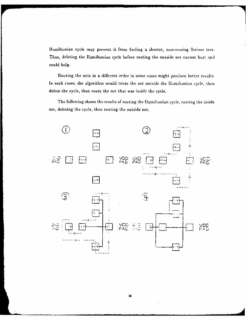
lamiltonian cycle may prevent it from finding a shorter, nuncrossing Steiner tree.
Thus, deleting the lamiltonian cycle before routing the outside net cannot hurt and
could help.
Routing the nets in a different order in sonic cases might produce better results.
In such cases, the algorithm would route the net outside the IHamiltonian cycle, then
delete the cycle, then route the net that was inside the cycle.
The following shows the results of routing the lamiltonian cycle, routing the inside
net, deleting the cycle, then routing the outside net.
:,D H HA
VOD GNmD H1 E El P AD PAD\lkr
-<-
53
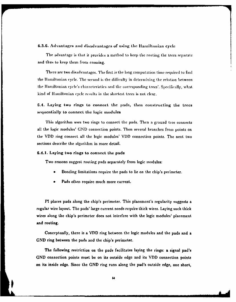
6.3.6. Advaiitages and lisadvantages of usinig tl, Ilainiftoitian cycle
The advantage is that it provides a method to kee l) tile routing the trees separate
and thus to keep tlhem from crossing.
There are two disadvantages. The first is the long computation time required to find
the I lanuilonian cycle. The second is the difficulty in determining the relation between
the Hlamiltonian cycle's characteristics and the corresponding trees'. Specifically, what
kind of Ilaniltonian cycle results in the shortest trees is not clear.
6.4. Laying two rings to connect the pads, then constructing tihe trees
sequentially to connect the logic modules
This algorithm uses two rings to connect the pads. Then a ground tree connects
all the logic modules' GND connection points. Then several branches from points on
the VDD ring connect all the logic modules' VDD connection points. The next two
sections describe the algorithm in more detail.
6.4.1. Laying two rings to connect the pads
Two reasons suggest routing pads separately from logic modules:
* Bonding limitations require the pads to lie on the chip's perimeter.
* Pads often require much more current.
PI places pads along the chip's perimeter. This placement's regularity suggests a
regular wire layout. The pads' large current needs require thick wires. Laying such thick
wires along the chip's perimeter does not interfere with the logic modules' placement
and routing.
Conceptually, there is a VDD ring between the logic modules and the pads and a
CND ring between the pads and the chip's perimeter.
The following restriction on the pads facilitates laying the rings: a signal pad's
CND connection points must be on its outside edge and its VDD connection points
on its inside edge. Since the GND ring runs along the pad's outside edge, one short,
54
st raight wire can connect the ring to the pad's GND connection points. If there were no
restrictions on the pads, local routing could connect the ring to the connection points.
The VDD ring's actual placement is that it runs along the signal pad's inside
edges. It is not truly a ring because there is a gap next to the GND pad. One reason
for this gap is that a wire must connect the GND pad to the logic modules. A solid
VDD ring would cut the GND pad off from the logic modules. Another reason is that
the gap ensures that the VDD wires form a tree.
The GNI) ring's actual placement is that it runs along the pads' outside edges.
A gap in the GND ring next to the VDD pad ensures that the GND wires form a
tree. Also, the GND rings avoids the corners of the chip, as some automatic handling
techniques require.
The following shows the complete VDD and GND rings.
_ LL_ _
6.4.2. Constructing the trees sequentially to connect the logic modules
Next, the algorithm constructs a CND tree to connect all the logic modules. The
CND pad has a GND connection point on its inside edge. The tree that will grow from
M.
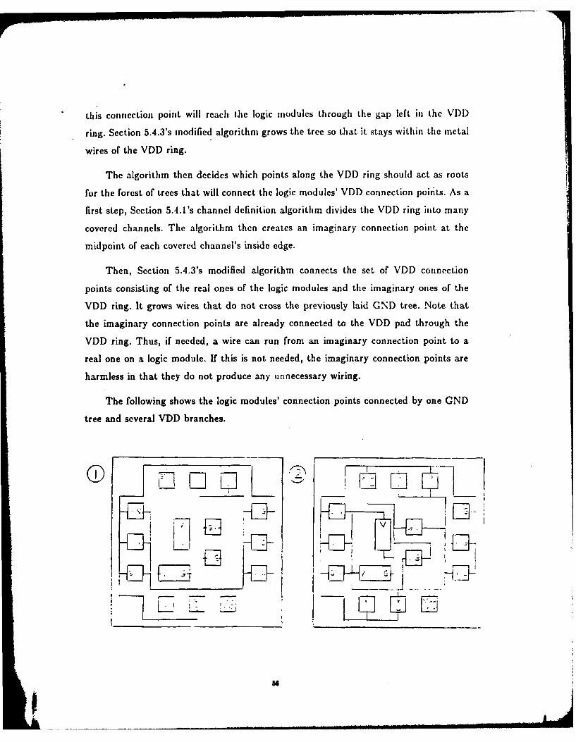
this connection point will reach the logic modules through the gap left in the VDI)
ring. Section 5.4.3's modified algorithm grows the tree so that it stays within tile metal
wires of the VDD ring.
The algorithm then decides which points along the VDD ring should act as roots
for the forest of trees that will connect the logic modules' VDD connection points. As a
first step, Section 5.4.1's channel definition algorithm divides the VDD ring into many
covered channels. The algorithm then creates an imaginary connection point at the
midpoint of each covered channel's inside edge.
Then, Section 5.4.3's modified algorithm connects the set of VDD connection
points consisting of the real ones of the logic modules and the imaginary ones of the
VDD ring. It grows wires that do not cross the previously laid GND tree. Note that
the imaginary connection points are already connected to the VDD pad through the
VDD ring. Thus, if needed, a wire can run from an imaginary connection point to a
real one on a logic module. If this is not needed, the imaginary connection points are
harmless in that they do not produce any unnecessary wiring.
The following shows the logic modules' connection points connected by one GND
tree and several VDD branches.
V -
1 ,
6.4.3. Advantages and disadvwtages of laying the rings and growing the trees
sequentially
The advantages of this algorithm are that it requires little computation time,
makes use of the pads' special placement, and produces short trees. The GNI) tree
is short because Section 5.4.3's algorithm produces short Steiner trees. The VDD tree
is short because the branches coming from many points on the VI)I) ring split the
problem of connecting the l VDD connection points into smaller, more easily solved
problems.
The disadvantage of this algorithm is that it makes certain assumptions on the
placement of the pads and connection points.
57
7. TIIE Ti EE-TRAVII SAL ALG OR ITI IM TI IAT
DETERM I NES WII E VIDTH
The preceding chapter presented several algorithms to construct two noncrossing
interdigitated trees. This chapter describes an algorithm that determines how wide
each wire in tile trees should be to carry tile current that will flow through it. during
the operation of the chip.
The following description of the algorithin traverses through one tree rooted at a
pad. PI's power-ground phase runs this algorithm twice, once for the VDD tree and
once for the GND tree.
After the algorithm has determined each wire's required width, it runs P1's resizing
algorithms to change the wire's dimensions until it attains its required width. The fact
that the tree-traversal algorithm works so closely with the resizer greatly influences
the algorithm's design.
One important feature of the resizer is that it resizes in one direction at a time.
For example, to adjust the placement of chip objects, it would resize in the x-direction,
then in the y-direction. Resizing in the x-direction means that the chip objects' vertical
sides are moved to different x-coordinates. Resizing in the y-direction means that the
horizontal sides are moved to different y-coordinates. These two resizings acieve the
desired placement of the chip objects.
The tree-traversal algorithm also considers only one direction at a time. It does
one tree-traversal for the x-direction and one for the y-direction.
Dealing with only one direction is often counterintuitive. One can consider a wire
as having a length and a width and the current as flowing along the wire. However,
applying these notions is more difficult when a wire is merely a rectangle in the plane.
Which dimension is the "length" is not clear. Its "length" could be less than its "width".
At intersections, the direction of current flow is not clear.
Thus, when the algorithm traverses the tree in the i-direction, it worries only
about whether the rectangle's horizontal dimension is sufficient to carry the current
5N
that will flow through the rectangle. It (foes not worry about the direction of current
flow.
The following description traverses the tree in the x-direction. Traversing in the
y-direction is similar.
Tile basic step in the tree traversal is adding the children's currents to find the
parent's current. Suppose that a wire comes from a pad and forks into two wires that
connect to two modules requiring 3 and 5 units of current. 3 units will flow through
one fork, 5 units through the other, and 8 through the base wire.
The algorithm traverses the tree in postorder, finding each child's current and then
summing to find the parent's current. As usual with a postorder traversal, the algorithm
recursively finds a child's current by finding its children's currents and summing.
The tree traversal finds the current for every wire of the tree. Multiplying by a
design rule constant gives each wire's required width. Then, for each wire, the algorithm
passes as parameters to the resizer the left side of the wire rectangle, the right side of
the wire rectangle, and the required width. Running the resizer adjusts the rectangle's
sides' placement so that the wire attains its required width.
The algorithm must define a tree node in a way that'is compatible with considering
only the x-direction. One'bree node often corresponds with one metal rectangle
representing a metal wire. The rectangle's left side is the node's left side and the
rectangle's right side is the node's right side.
In some cases, one tree node could be several rectangles. Suppose there are
several rectangles lined up horizontally. The rectangles' bottom sides have the same
y-coordinate, and their top sides have the same y-coordinate. In this case, the node's
left side is the leftmost rectangle's left side, and the node's right side is the rightmost
rectangle's right side.
5,
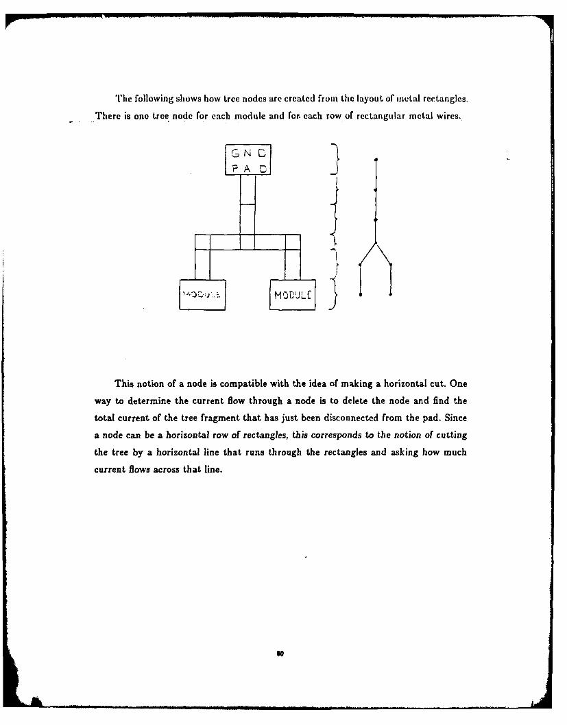
Trhe following shows how tree niodes are created from itth layout or metal rectangles.
There is one tree node for each module and for. each row of rectangular metal wires.
This notion of a node is compatible with the idea of making a horizontal cut. One
way to determine the current flow through a node is to delete the node and find the
total current of the tree fragment that has just been disconnected from the pad. Since
a node can be a horizontal row of rectangles, this corresponds to the notion of cutting
the tree by a horizontal line that runs through the rectangles and asking how much
current flows across that line.
so
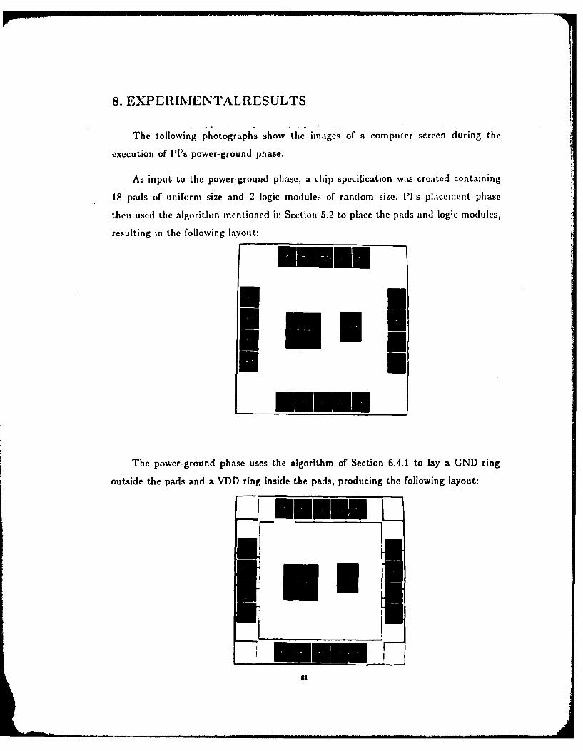
8. EXPERIMENTALRESULTS
The tollowing photographs show the images of a computer screen during the
execution of PI's power-ground phase.
As input to the power-ground phase, a chip specification w;s created containing
18 pads of uniform size and 2 logic modules of random size. P1's placement phase
then used the algorithm mentioned in Section 5.2 to place the pads and logic modules,
resulting in the following layout:
-o-U I!
IEmEUI Um
.ME-
The power-ground phase uses the algorithm of Section 6.4.1 to lay a GND ring
outside the pads and a VDD ring inside the pads, producing the following layout:
_ I L ___
II/SI
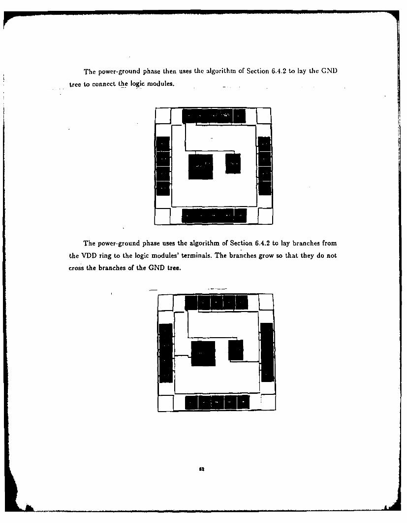
Tie power-ground phase then uses the algorithm of Section 6.4.2 to lay the GND
tree to connect the logic modules.
The power-ground phase uses the algorithm of Section 6.4.2 to lay branches from
the VDD ring to the logic modules' terminals. The branches grow so that they do not
cross the branches of the GND tree.
LIL
L MENEM-
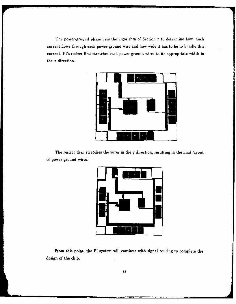
The power-ground phase uses the algorithm of Section 7 to determine how much
current flows through each power-ground wire and how wide it has to be to handle this
current. P1's resizer first stretches' each power-ground wires to its appropriate width in
the x direction.
The resizer then stretches the wires in the y direction, resulting in the final layout
of power-ground wires.
From this point, the PI system will continue with signal routing to complete the
design of the chip.
63
9. PROBLEMS FOR FUITIER IESEARCII
It is not known whether the following problem is NP-complete:
Given two sets of points in the plane, find two noncrossing Steiner trees
such that one tree spans one set, the other tree spans the other set, and
the trees' combined length is niniinum.
The metric for determining lengt li can be eit her Elulcidean ( X( .- )' _* ('- -Y yl ' ) or
Manhattan (IX2 - III + IY2 - YI I). Since this problem models the power-ground problen,
knowing its complexity would greatly influence this part of VLSI research.
Using the lamiltonian cycle to divide the chip into separate routing regions raises
the question of how the cycle's characteristics relate to the resulting tree's length and
other characteristcs.
This suggests a more general question of the best method to divide the chip into
routing regions. There are three such methods in this thesis:
0 Section 6.3's Ilamiltonian cycle separating GND routing from VDD
routing.
* Section 6.4's VDD ring separating logic module routing from pad routing.
0 Rothermel and Mlynski's method, described in Section 4.2, separating
routing the chip's left half from routing the right half.
Further research could determine how effective each method is at constructing short
trees and could develop new methods for creating separate routing regions.
The goal of the algorithms of this thesis is to minimize the amount of metal used by
the trees. Further research might reveal other desirable characteristics the trees should
possess. An interesting part of this aspect would be to determine what characteristics
of the trees result in better signal routing.
6A
10. CONCLUSIONS
As the preceding chapter shows, ll's power-ground phase successfully automates
the power-ground phase of chip design. Tie algorithm's high success rate, its low
running time, and the high quality of its output make it a useful tool in chip design.
The research that produced the algorithms explored the similarities an(d differences
between signal routing and power-ground routing. It showed that many signal-routing
techniques are applical)e to power-groun(d routing.
Through its application of signal-routing techniques, the research showed new
applications of techniques in graph theory, such as growing Steiner trees.
To keep the trees from crossing, the algorithm introduced the idea of using a
Hlamiltonian cycle to separate the chip into two separate routing regions. By extension,
using this concept in other situations could control the growth of trees. Extending
the idea of separate routing regions, other lines besides a Hamiltonian cycle could
control tree growth. For example, the VDD ring, described in Section 6.4, separates
logic module routing from pad routing. This relates to Rothermel and Mlynski's work,
where a vertical line divides the chip into two routing regions.
65
II. BIABLIOCRAPtlY
[1181) Baratz, Alan. A Graph Theoretic VLSI Layout Procedure, Ili. D. rhesis,N'lassachusetts Institute of Technology, August, 1981.
I(79] Nicos ('hristolides. "ili'raveliig Salesnan Problem", Chapter 6, CombinatorialOptimization, Wiley , Sons, 1979, pages 1.18-149.
[(CJ79Michael R. Garey an( David S. Johnson. Computers and Intractability: A Guideto the Theory of NP- Completeness, Freeman and Company, 1979, page 209.
[11821 llassett, James E. "Automated Layout in ASIILAR: An Approach to the Prohlemsof 'General Cell' Layout for VLSr", ACM IEEt, Nineteenth Designl AutomationConference Proceedings, .July, 1982, pages 777-784.
1,11080] Lhota, Frank J. Dual Spanning Trees. Term paper for Course 6.85.1,Massachusetts Institute of Technology, May, 1980.
[1,1182] Lie, Margaret, and Chi-Song florng. "A Bus Router for IC Layout", ACMIEEE Nineteenth Design Automation Conference Proceedings, July, 1982, pages129-132.
[LIN651 Lin, Shen. "Some Computer Solutions of the Traveling-Salesman Problem",Bell System Technical Journal 44, 2245-2269 (1965).
[MC80] Mead, C. A., and L. A. Conway. Introduction to VLSI Systems, Addison-WesleyPublishing Co., Reading, Massachusetts, 1980.
[M083] Moulton, Andrew. "Laying the Power and Ground Wires on a VLSI Chip",ACM IEE, 20th Design Automation Conference, 1983, pages 754-755.
[IZ182] Rivest, Ronald L. "The 'PI' (Placement and Interconnect) System", ACM IEEENineteenth Design Automation Conference Proceedings, July, 1982, pages 475-481.
[ltM81] Rothermel, 11-J., and D. A. Mlynski. "Computation of Power Supply Nets inVLSI Layout", AGM IEEE Eighteenth Design Automation Conference Proceedings,1981, pages 37-42.
[S082] Syed, Zahir A., and Abbas El Gamal. "Single Layer Routing of Power andGround Networks in Integrated Circuits", Journal of Digital Systems, Volume VI,Number 1, Spring, 1982, pages 53-63.
[SGJ382] Syed, Zahir A., Abbas El Gamal, and M. A. Breuer. "On Routing for CustomIntegrated Circuits", ACM IEEE Nineteenth Design Automation ConferenceProceedings, July, 1982, pages 887-893.
66
IiA
OFFICIAL DISTRIBUTION LIST
1984
Director 2 CopiesInformation Processing Techniques OfficeDefense Advanced Research Projects Agency1400 Wilson BoulevardArlington, VA 22209
Office of Naval Research 2 Copies800 North Quincy StreetArlington, VA 22217Attn: Dr. R. Grafton, Code 433
Director, Code 2627 6 CopiesNaval Research LaboratoryWashington, DC 20375
Defense Technical Information Center 12 CopiesCameron StationAlexandria, VA 22314
National Science Foundation 2 CopiesOffice of Computing Activities1800 G. Street, N.W.Washington, DC 20550Attn: Program Director
Dr. E.B. Royce, Code 38 1 CopyHead, Research DepartmentNaval Weapons CenterChina Lake, CA 93555
Dr. G. Hopper, USNR 1 CopyNAVDAC-OOHDepartment of the NavyWashington, DC 20374