Embed Size (px)
Citation preview
FACULDADE DE ENGENHARIA DA UNIVERSIDADE DO PORTO
The Impact of Timer Resolution in theEfficiency Optimization of Synchronous
Buck Converters
Pedro Amaral
FOR JURY EVALUATION
MESTRADO INTEGRADO EM ENGENHARIA ELETROTÉCNICA E DE COMPUTADORES
Supervisor: Cândido Duarte (FEUP)
Co-Supervisor: Pedro Costa (Infineon Technologies AG)
June 29, 2015

c© Pedro Amaral, 2015

Abstract
Power efficiency is now, more than ever, a major topic for systems, households, providers andgovernments. The amount of electronic devices has increased exponentially in the last decade,and the growth rhythm is not estimated to slow down. Due to an imminent energy crisis and theinability of power suppliers to easily step up their production, the stress of reducing consumption,increasing efficiency and minimizing the power stage footprints is passed through to the systemproviders.
The switching frequency of power converters is driving the footprint reduction by enablingsmaller components (e.g. coils, capacitors, etc), but at the same time imposing another levelof optimization in some variables of a power converter. One of the variables that most impactsthe efficiency of the converter is linked to the non-optimization of the dead time in synchronousswitching. Simultaneously, the market of non-digital power supplies is steadily losing ground tothe digitalized counterparts. This creates new possibilities to tackle old issues with unprecedentedapproaches and create business and innovation opportunities.
This dissertation aims at analyzing the influence of one of the most important characteristicsof a digital controller, the timer resolution, in the issue of dead time optimization for synchronousbuck converters. An algorithm has been designed and implemented using state-of-the-art hardwarefrom Infineon Technologies to prove the concept and demonstrate the results.
i

ii
Resumo
A eficiência energética é hoje, mais do que nunca, um tema preponderante em sistemas, lares,produtores e administração. A quantidade de aparelhos electrónicos tem crescido exponencial-mente na última década e o ritmo não dá sinais de abrandamento. Devido à iminente crise en-ergética e à incapacidade dos fornecedores de energia em aumentar rapidamente a sua produção, apressão para reduzir o consumo, aumentar a eficiência e minimizar o tamanho e custo de andaresde potência é transmitida para o lado dos fornecedores de sistemas.
A frequência de comutação em conversores de potência tem liderado a redução do seu custopela diminuição do tamanho dos componentes (como bobinas e condensadores), mas simultanea-mente tem imposto um outro nível de optimização das variáveis. Uma dessas variáveis que maisinfluencia a eficiência do conversor está ligada à não optimização do tempo morto em conversoressíncronos. Simultaneamente, o mercado das fontes de potência não-digitais tem vindo a perder ter-reno para os equivalentes digitais. Isto cria novas possibilidades para abordar problemas antigoscom recursos nunca utilizados e assim criar oportunidades de inovação e negócio.
Esta dissertação tem como objectivo analizar a influência de uma das características mais im-portantes em controladores digitais, a resolução do timer, na questão da optimização do tempomorto em conversores abaixadores síncronos. Será desenhado e implementado um algoritmo emtecnologia moderna da Infineon Technologies de forma a provar o conceito e demonstrar os resul-tados.
iii

iv

Acknowledgments
I would like to start by thanking my supervisors, Cândido Duarte, for his constant supportand dedication, scientific experience and helpful advices, and Pedro Costa, for his vast industrialbackground, the idea of this dissertation and his valuable guidance. Without them, this work wouldhave never taken off.
Furthermore, I would like to acknowledge the engineers of Infineon Technologies AG, whohave directly or indirectly contributed to this dissertation, and the technical staff of the Departmentof Electrical Engineering of this Faculty, for promptly fulfilling my requests.
Moreover, I would like to express my gratitude to my family for supporting me, not onlythrough the duration of this dissertation, but also during the 5 years I had in this university.
I would also like to thank my friends, not only for the valuable technical insights, but forthe support, friendship and companionship. If anything, we all had a good laugh over this wholedissertation deal.
Finally, I would like to thank my girlfriend Jenny, for being the wideband low-pass filter to myhigh switching frequency mood oscillator. Her support and encouragement was invaluable. Thankyou.
Pedro Amaral
v

vi

“There is only one way to avoid criticism:do nothing, say nothing, and be nothing.”
Aristotle
vii

viii

Contents
Abstract i
Resumo iii
1 Introduction 11.1 Objectives of this Work . . . . . . . . . . . . . . . . . . . . . . . . . . . . . . . 51.2 Organization of the Dissertation . . . . . . . . . . . . . . . . . . . . . . . . . . 6
2 Literature Review 72.1 Fixed dead times . . . . . . . . . . . . . . . . . . . . . . . . . . . . . . . . . . 72.2 Switching current sensing . . . . . . . . . . . . . . . . . . . . . . . . . . . . . . 82.3 Switching voltage sensing . . . . . . . . . . . . . . . . . . . . . . . . . . . . . 8
2.3.1 Adaptive control . . . . . . . . . . . . . . . . . . . . . . . . . . . . . . 92.3.2 Predictive control . . . . . . . . . . . . . . . . . . . . . . . . . . . . . . 10
2.4 Sensorless methods . . . . . . . . . . . . . . . . . . . . . . . . . . . . . . . . . 112.5 Summary and discussion . . . . . . . . . . . . . . . . . . . . . . . . . . . . . . 14
3 Analysis of Dead Time Optimization 173.1 Modeling of the Algorithm . . . . . . . . . . . . . . . . . . . . . . . . . . . . . 173.2 Operation Limits . . . . . . . . . . . . . . . . . . . . . . . . . . . . . . . . . . 203.3 Resource Usage . . . . . . . . . . . . . . . . . . . . . . . . . . . . . . . . . . . 223.4 Power Efficiency Improvement . . . . . . . . . . . . . . . . . . . . . . . . . . . 233.5 Summary . . . . . . . . . . . . . . . . . . . . . . . . . . . . . . . . . . . . . . 26
4 Experimental Results 294.1 Powertrain and Microcontroller Unit . . . . . . . . . . . . . . . . . . . . . . . . 294.2 Software and Algorithm . . . . . . . . . . . . . . . . . . . . . . . . . . . . . . 324.3 Measurements and Results . . . . . . . . . . . . . . . . . . . . . . . . . . . . . 364.4 Simulations . . . . . . . . . . . . . . . . . . . . . . . . . . . . . . . . . . . . . 41
5 Conclusions and Future Work 435.1 Fulfillment of the Objectives . . . . . . . . . . . . . . . . . . . . . . . . . . . . 435.2 Future Work . . . . . . . . . . . . . . . . . . . . . . . . . . . . . . . . . . . . . 44
A Calculation of Real Dead Time 47
B Results of the Simulation 49
ix

x CONTENTS
List of Figures
1.1 Synchronous buck converter. . . . . . . . . . . . . . . . . . . . . . . . . . . . . 21.2 Typical waveforms of a buck converter. . . . . . . . . . . . . . . . . . . . . . . 31.3 Rising edge and falling edge dead times. . . . . . . . . . . . . . . . . . . . . . . 41.4 The current flow through the transistors and the body diode. . . . . . . . . . . . 41.5 The steady growth on the market of digitalized power supplies. . . . . . . . . . . 5
2.1 Fixed dead time approach . . . . . . . . . . . . . . . . . . . . . . . . . . . . . . 82.2 Switching current sensing method . . . . . . . . . . . . . . . . . . . . . . . . . 92.3 Adaptive optimization methods . . . . . . . . . . . . . . . . . . . . . . . . . . . 92.4 Non-optimal and optimal switching waveforms . . . . . . . . . . . . . . . . . . 112.5 Maximum Efficiency Point Tracking algorithm . . . . . . . . . . . . . . . . . . 122.6 Accumulator and input current method for sensorless optimization . . . . . . . . 132.7 Sensorless dead time optimization using duty cycle minimization . . . . . . . . . 13
3.1 Switching node voltage vsw. . . . . . . . . . . . . . . . . . . . . . . . . . . . . . 183.2 The four sequential stages of the dead time optimization algorithm. . . . . . . . . 193.3 Representation in IR3 of the set of possible operation points r . . . . . . . . . . . 203.4 Example of a set of possible operation points defined by the resources of the con-
troller. . . . . . . . . . . . . . . . . . . . . . . . . . . . . . . . . . . . . . . . . 213.5 Dependency of ϕ on Ntimer and NADC. . . . . . . . . . . . . . . . . . . . . . . . 233.6 Depictions of Ψ(γ). . . . . . . . . . . . . . . . . . . . . . . . . . . . . . . . . . 253.7 Dependency of the efficiency improvement factor Ψ with ADC and timer resolution. 26
4.1 The proof-of-concept prototype: buck converter kit and XMC4200 control card. . 304.2 A view of the microcontroller peripherals required by the project. . . . . . . . . . 304.3 High-side current sensing for calculation of the power efficiency. . . . . . . . . . 314.4 The buck converter and its control law, realized on a XMC4200 microcontroller. . 324.5 Generation of an High Resolution PWM waveform. . . . . . . . . . . . . . . . . 334.6 The illustrative relation between dead time and duty cycle. . . . . . . . . . . . . 344.7 Flowchart of the sensorless dead optimization algorithm. . . . . . . . . . . . . . 354.8 Screenshot of the xSPY interface designed to control and debug the algorithm. . . 374.9 Duty cycle variation after manually triggering the algorithm. Running time is 80 ms. 374.10 Duty cycle response to changes in rising edge dead time followed by falling edge
dead time. . . . . . . . . . . . . . . . . . . . . . . . . . . . . . . . . . . . . . . 384.11 Buck converter control signals measured with an oscilloscope. . . . . . . . . . . 404.12 Relation between temperatures of control and synchronous MOSFETs and dead
time. . . . . . . . . . . . . . . . . . . . . . . . . . . . . . . . . . . . . . . . . . 414.13 Simulation model used in Simulink. . . . . . . . . . . . . . . . . . . . . . . . . 424.14 Simulation results for different NADC curves. . . . . . . . . . . . . . . . . . . . . 42
xi

xii LIST OF FIGURES
A.1 Representation of the delay between the signal out of the microcontroller pins andthe switching node voltage. . . . . . . . . . . . . . . . . . . . . . . . . . . . . . 47
A.2 Oscilloscope print of the difference between defined and real dead time for bothedges. The two signals are measured at the output pins of the microcontrollerwhile the bottom one is measured at the swithing node voltage. . . . . . . . . . . 48
B.1 Results of the simulation. . . . . . . . . . . . . . . . . . . . . . . . . . . . . . . 50

List of Tables
2.1 Summary of proposed dead time optimization methods and their claimed results. 15
4.1 Operation parameters for the prototype buck converter. . . . . . . . . . . . . . . 294.2 Experimental results using both low and high resolution PWM. . . . . . . . . . . 39
A.1 Time parameters that affect the signal. . . . . . . . . . . . . . . . . . . . . . . . 48
xiii

xiv LIST OF TABLES

Abbreviations
AC Alternate CurrentADC Analog to Digital ConverterCCM Continuous Conduction ModeCS Control SwitchDC Direct CurrentDCM Descontinuous Conduction ModeDPWM Digital Pulse Width ModulationDSP Digital Signal ProcessorDTLL Dead Time Locked-LoopFPGA Field Programmable Gate ArrayFS Full ScaleHRPWM High Resolution Pulse Width ModulationIC Integrated CircuitMOSFET Metal Oxide Semiconductor Field Effect TransistorMEPT Maximum Efficiency Point TrackingMPPT Maximum Power Point TrackingPI Proportial IntegralPWM Pulse-Width ModulationSMPS Switched Mode Power SupplySS Synchronous Switch
xv


Chapter 1
Introduction
Since the dawn of electrical engineering, power conversion has been one of the most important
disciplines in the area. From the 19th century until the present day, engineers have come up with an
incredible variety of electric energy sources and applications. However, these two are not always
related, neither in geographic nor in operational terms. The conversion from and into different
voltage, current and frequency levels was and still is pivotal to deliver electricity to billions of
people, propel the development of new technologies and fuel the modern machinery that supports
our society.
But we live in a different time. We are able to transport energy for very long distances and
convert it in many ways, but the global energetic and environmental situation pushes us one step
forward: we must do it efficiently. This means that the scientific community must pose questions
and rethink even the most established design principles in electrical engineering.
Power converters can be divided into four different classes:
1. AC/DC (rectifiers);
2. DC/AC (inverters);
3. DC/DC;
4. AC/AC (transformers).
DC/DC converters are the type of circuit used to convert a direct current supply from one
voltage level to another. One family of DC/DC converters are the linear voltage regulators. These
circuits act like variable resistors that continuously adjust a voltage divider in order to supply a
steady average output voltage. However, they dissipate the extra energy as heat. Switched-mode
converters (commonly called DC/DC converters due to their popularity) on the other hand, use
a storage element (capacitor or inductor) that is charged and discharged continuously by driving
switching elements. Switched-mode converters are much more efficient than linear regulators
(theorically, up to 100 %) and have become extremely popular with the declining prices of power
switches.
Switched-mode DC/DC converters are available in many topologies, namely buck, boost,
buck-boost, Cuk, full-bridge, split-pi, SEPIC, zeta, etc. In this dissertation, the focus will be on
1
2 Introduction
buck converters, as they find their way in a wide variety of applications: residential, commercial,
industrial, aerospace, transportation, utilities and telecommunications [1].
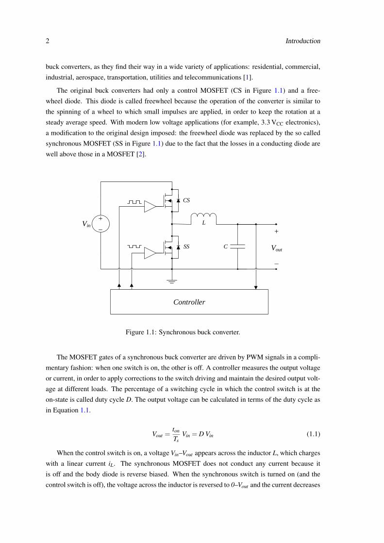
The original buck converters had only a control MOSFET (CS in Figure 1.1) and a free-
wheel diode. This diode is called freewheel because the operation of the converter is similar to
the spinning of a wheel to which small impulses are applied, in order to keep the rotation at a
steady average speed. With modern low voltage applications (for example, 3.3 VCC electronics),
a modification to the original design imposed: the freewheel diode was replaced by the so called
synchronous MOSFET (SS in Figure 1.1) due to the fact that the losses in a conducting diode are
well above those in a MOSFET [2].
CS
SS
VinL
C Vout
+
Controller
Figure 1.1: Synchronous buck converter.
The MOSFET gates of a synchronous buck converter are driven by PWM signals in a compli-
mentary fashion: when one switch is on, the other is off. A controller measures the output voltage
or current, in order to apply corrections to the switch driving and maintain the desired output volt-
age at different loads. The percentage of a switching cycle in which the control switch is at the
on-state is called duty cycle D. The output voltage can be calculated in terms of the duty cycle as
in Equation 1.1.
Vout =ton
TsVin = D Vin (1.1)
When the control switch is on, a voltage Vin–Vout appears across the inductor L, which charges
with a linear current iL. The synchronous MOSFET does not conduct any current because it
is off and the body diode is reverse biased. When the synchronous switch is turned on (and the
control switch is off), the voltage across the inductor is reversed to 0–Vout and the current decreases
Introduction 3
linearly as the inductor discharges. This current also flows through the synchronous MOSFET. The
capacitor C acts as a filter in order to keep Vout within an acceptable ripple (Figure 1.2).
Vout
Vin Vout
ton toff
Ts
CS
SS
vL
iLIL=Iout
vOUT
Vout
Figure 1.2: Typical waveforms of a buck converter.
For medium to heavy loads (Iout), the inductor current never reaches zero, which means the
converter is operating on Continuous Conduction Mode (CCM) as seen in Figure 1.2. If the
load is light, the inductor current reaches zero and the converter enters Discontinuous Conduction
Mode (DCM). In DCM, the switches can be operated normally, in fixed switching frequency (as
in CCM), or in a variable frequency mode, known as pulse-skipping. Pulse-skipping increases the
efficiency at light loads by reducing the switching losses [3].
In practice, the turn-on of a MOSFET is not instantaneous, which means that a dead time must
be added to the PWM waveform in order to prevent a short-circuit between supply and ground
(see Figure 1.3). This would cause a high shoot-through current to flow through the transistors,
increasing losses and possibly destroying both MOSFETs. Dead time is also called "blanking
time" or simply "delay".
In unoptimized systems, this dead time is safely set to the worst-case scenario: a time interval
large enough to account for the highest possible load and temperature conditions. However, when
both MOSFETs are off, even though the synchronous switch is not conducting, the body diode is
4 Introduction
CS
SS
td,r
tontoff
td,f
Figure 1.3: Rising edge and falling edge dead times.
forward biased and current is flowing through it, as shown in Figure 1.4. As previously mentioned,
a conducting diode has much higher losses than a conducting MOSFET, which means that the
existence of dead time decreases the general efficiency of a converter.
CS
SS
CS
SS
CS
SS
CS
SS
Figure 1.4: The current flow through the transistors and the body diode.
Fortunately, it is not necessary to fix the dead times for the entire operation of the converter.
Several dead time optimization methods have been proposed to dynamically adjust both rising and
falling edge dead times and, consequently, improve the converter power efficiency. This disserta-
tion proposes an approach to this issue.

1.1 Objectives of this Work 5
1.1 Objectives of this Work
In the last decade, the world market for digitalized power converters has been growing steadily.
Digital control introduces features that are not possible in non-digital power supplies, such as
communication and diagnostic capabilities. Efficiency can be also addressed with digital control,
for example, in the ability to enter different operation modes for particular loads. The decline of
microprocessor and microcontroller costs is making digitalized power converters more attractive
over the years and the tendency is not stopping, as seen in Figure 1.5. Top technology companies
such as Infineon, Microchip, TI and Freescale are investing in these products and widening their
portfolios to meet the most demanding customer requirements.
Figure 1.5: The steady growth on the market of digitalized power supplies.
That said, it is scientifically and industrially relevant to address the topic of dead time opti-
mization in light of the use of digital control, particularly microcontrollers.
This dissertation has the following objectives:
• Investigate the relation of an important feature of any digital controller, the timer resolution,
with the power efficiency improvement that dead time optimization can offer;
• Design and test an optimization algorithm in a proof-of-concept experimental setup;
• Achieve an algorithm that is simple, computationally inexpensive, effective and cheap to
implement, seemlessly taking advantage of the digital controller to resolve the issue of
dead time induced power losses.

6 Introduction
The new Infineon Technologies Buck Kit will be used as powertrain for the prototype. The
control will be performed on a XMC4200 microcontroller and will take advantage of the inno-
vative High-Resolution PWM module (HRPWM). The XMC family is the world’s first ARM
Cortex-based microcontroller to offer a DPWM resolution of only 150 ps [4].
1.2 Organization of the Dissertation
After this introduction, a literature review on the topic of dead time optimization will be made
in Chapter 2. Different approaches to the theme applied in buck converters will be explored and
compared to each other.
In Chapter 3, a theoretical analysis of the problem will be done: the buck converter will be
analyzed and the operation of an hypothetical algorithm will be related to the characteristics of
a generic digital controller. The impact of said characteristics on power efficiency will also be
deducted.
Chapter 4 presents a concrete design and implementation of an optimization algorithm. The
hardware and software are exposed and discussed. The results are to be presented and related to
ones expected from the previous chapter.
The document will end with the conclusions, a balance of the fulfillment of the objectives and
suggestions for future work.

Chapter 2
Literature Review
The reduction of power losses by optimization of dead times has been the goal of many aca-
demic and industrial publications. There are several proposed methods using different technolo-
gies which can be classified as follows:
1. Fixed dead times;
2. Based on the sensing of switching currents;
3. Based on the sensing of switching voltages:
(a) Adaptive;
(b) Predictive;
4. Sensorless.
In this chapter, a literature review of the mentioned optimization methods will be done, along
with explanations to the peculiarities of certain approaches, illustrated examples and an analysis
of advantages and disadvantages to each method.
2.1 Fixed dead times
The fixed dead time control (sometimes referred to as the first generation) is the simplest
method but yields the worst performance. It simply consists of choosing a rising edge and falling
edge dead time period that stays constant throughout the entire operation. The chosen td,r and td, fmust be long enough to account for the worst case scenario in terms of process, temperature and
load variations, which leads inevitably to a reduced power efficiency, mostly due to unnecessary
body diode conduction. This method can be implemented with a cross-coupled latch with delay as
explained by Ramachandran in [5] and shown in Figure 2.1. Furthermore, most microcontroller
timers and PWM generation ICs also include complementary operation modes with fixed dead
time insertion [6].
7
8 Literature Review
delay
delay
PWM in
Figure 2.1: Fixed dead time approach [5].
2.2 Switching current sensing
The methods based on switching current sensing are based on the idea of preventing overlap-
ping gate driving commands by measuring the current flowing through the synchronous MOSFET
and detecting shoot-through currents (a basic set-up can be seen in Figure 2.2). When this high
current is detected, the dead times should be increased to prevent overlapping. Otherwise, they
should be decreased [7]. In Huang et al. [8] a more advanced method is proposed. By monitor-
ing the switching current, the authors are able to estimate the load and quickly adjust the dead
times accordingly, using a digitally implemented tri-mode controller. Despite the power efficiency
improvement (up to 5 % in [8]), the fact that these methods depend on high-bandwidth current
sensors (such as the “SENSEFET” technology, proposed in [9] and applied in [8]) makes their
implementation difficult and sometimes impracticable.
2.3 Switching voltage sensing
The most common dead time control methods in the scientific literature are those based on
switching voltage measurement. They are normally sub-divided into the adaptive and predictive
type. The adaptive control (also known as second generation methods) consists of measuring the
switching voltage across the synchronous rectifier and adjusting the dead times accordingly and
on-the-fly. The predictive control (also called third generation methods) differs from the adaptive
counterpart by using the information from the previous switching cycle to set the best possible
dead time in the current cycle. In the following subsections, some examples of both technologies
will be presented and discussed.
2.3 Switching voltage sensing 9
Figure 2.2: Switching current sensing method - basic setup for shoot-through current detection [7].
2.3.1 Adaptive control
A concrete example of an adaptive optimization method is presented in Mappus [10]: as shown
in Figure 2.3a, a simple logic circuit is able to detect the zero-voltage crossing at the synchronous
rectifier and avoid prolonged body diode conduction by closing it. This emulates the behavior of
an ideal diode. The work presented in Krein et al. [11] is in fact one of the first articles to emulate
multiple switching devices with a MOSFET, including the ideal diode (see Figure 2.3b).
PWM in
(a) (b)
Figure 2.3: Adaptive optimization methods: (a) Adaptive gate driving circuit [10] and (b) Idealdiode emulation [11].
The same concept is used by Lau et al. [12] and Acker et al. [13]: when the control MOSFET
is turned off, the switch node voltage drops from Vin to zero. A comparator detects the zero
crossing and immediately turns on the synchronous MOSFET to avoid body diode conduction.
Similarly, when the synchronous rectifier is turned off, the body diode is forward biased and the
10 Literature Review
drain to source voltage goes from zero to negative. By detecting this instant, the control MOSFET
is immediately turned on to prevent further diode conduction losses.
The advantages of adaptive control methods are very relevant, particularly when compared to
the fixed dead time solution: they allow on-the-fly adjustment for different MOSFETs, temperature
and operation conditions. However, despite their popularity, adaptive methods still have some
drawbacks: the sensing of the noisy switching voltage, the need for high-speed comparators and
the non-compensated MOSFET gate driving delays, which make the adaptive control methods
especially ineffective at high switching frequencies.
2.3.2 Predictive control
To overcome the problems mentioned in the previous subsection, the third generation of dead
time control methods appeared: the predictive type.
S. Mappus [10] proposes a method that is based on the premise that the dead time required for
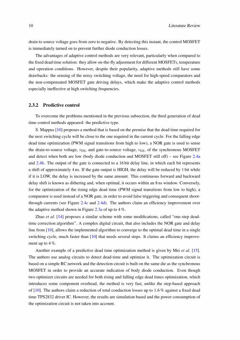
the next switching cycle will be close to the one required in the current cycle. For the falling edge
dead time optimization (PWM signal transitions from high to low), a NOR gate is used to sense
the drain-to-source voltage, vDS, and gate-to-source voltage, vGS, of the synchronous MOSFET
and detect when both are low (body diode conduction and MOSFET still off) – see Figure 2.4a
and 2.4b. The output of the gate is connected to a 16 bit delay line, in which each bit represents
a shift of approximately 4 ns. If the gate output is HIGH, the delay will be reduced by 1 bit while
if it is LOW, the delay is increased by the same amount. This continuous forward and backward
delay shift is known as dithering and, when optimal, it occurs within an 8 ns window. Conversely,
for the optimization of the rising edge dead time (PWM signal transitions from low to high), a
comparator is used instead of a NOR gate, in order to avoid false triggering and consequent shoot-
through currents (see Figure 2.4c and 2.4d). The authors claim an efficiency improvement over
the adaptive method shown in Figure 2.3a of up to 4 %.
Zhao et al. [14] proposes a similar scheme with some modifications, called “one-step dead-
time correction algorithm”. A complex digital circuit, that also includes the NOR gate and delay
line from [10], allows the implemented algorithm to converge to the optimal dead time in a single
switching cycle, much faster than [10] that needs several steps. It claims an efficiency improve-
ment up to 4 %.
Another example of a predictive dead time optimization method is given by Mei et al. [15].
The authors use analog circuits to detect dead-time and optimize it. The optimization circuit is
based on a simple RC network and the detection circuit is built on the same die as the synchronous
MOSFET in order to provide an accurate indication of body diode conduction. Even though
two optimizer circuits are needed for both rising and falling edge dead times optimization, which
introduces some component overhead, the method is very fast, unlike the step-based approach
of [10]. The authors claim a reduction of total conduction losses up to 1.6 % against a fixed dead
time TPS2832 driver IC. However, the results are simulation based and the power consumption of
the optimization circuit is not taken into account.
2.4 Sensorless methods 11
V
t0 V
VTH
VDS VGSNOR gate
(a)
V
t0 V
VTH
VDS VGS
(b)
V
t0 V
VGS VDSComparator
Output
-0.3 V
(c)
V
t0 V
VGS VDS
(d)
Figure 2.4: Non-optimal and optimal switching waveforms [10]: (a) Non-optimal falling edgeswitching, (b) optimal falling edge switching, (c) non-optimal rising edge switching, (d) optimalrising edge switching.
Trescases et al. [16] is also commonly referenced in the literature. This paper presents a
predictive method based on an analog Dead-Time Locked-Loop (DTLL). Two comparators sense
the drain-to-source voltage vDS (to detect the zero-voltage crossing) and the gate-to-source voltage
vGS (to detect the threshold voltage crossing). The comparators are followed by a phase detector
that provides up and down pulses for a charge pump. The charge pump then outputs a linear
delay control voltage that determines the dead time for the MOSFET under control, completing
the feedback loop. Both the control and synchronous MOSFET have a DTLL block to drive them,
which introduces some overhead. However, the experimental results show a significative reduction
in body diode losses.
2.4 Sensorless methods
In spite of their undeniable ingenuity and results, the previously mentioned techniques always
rely on external circuitry. This can bring cost and effort overhead as well as added power con-
sumption, which counters the benefits of adding said circuitry. Sensorless methods are the answer
for applications where extra components cannot be added. They depend exclusively on parameters
that are already measured for control or protection of the converter.
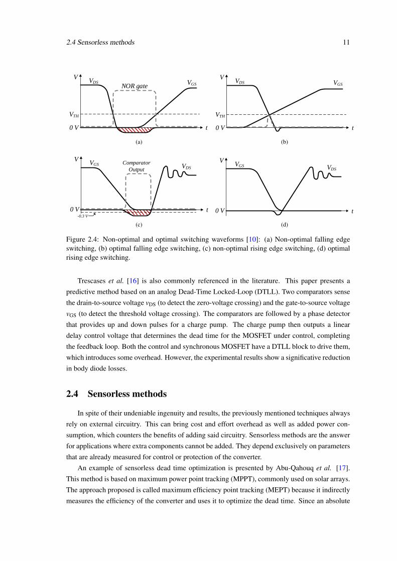
An example of sensorless dead time optimization is presented by Abu-Qahouq et al. [17].
This method is based on maximum power point tracking (MPPT), commonly used on solar arrays.
The approach proposed is called maximum efficiency point tracking (MEPT) because it indirectly
measures the efficiency of the converter and uses it to optimize the dead time. Since an absolute
12 Literature Review
value of the efficiency is not required, only the input current, Iin, is monitored. The algorithm
evaluates the signal of the gradient of the input current and the dead time shift. If they are the
same, the time step should be added to the current dead time. Conversely, if they are opposite,
the current dead time should be subtracted a time step. The search stops when the operation point
of minimal input current (maximum efficiency) is found, as seen in Figure 2.5. Despite being
comparatively slow and thus unsuitable for applications with a fast varying load, this method
yields good results with a claimed efficiency improvement of 2 %.
Efficiency
Dead time (td)
light load
mid load
full load
td1 td2 td3
Figure 2.5: Maximum Efficiency Point Tracking algorithm [17].
Pizzutelli et al. [18] proposes another sensorless dead time control method based on input
current. It claims to improve over [17] because it can never get stuck at local minima and it is
suitable for high efficiency (>90 %) applications, where the small current variations cannot be
easily measured. In this method, a compare algorithm is used to test two different dead times and
choose the one that yields the highest efficiency. This is achieved by summing the input current
to an accumulator while one dead time is applied and subtracting while the other dead time is
applied. After multiple cycles, the signal of the result from the accumulator indicates which of
the dead time values produced a lower input current and consequently a higher efficiency (see
Figure 2.6). The authors use the compare algorithm iteratively in a global search algorithm that is
capable of ignoring local minima. The experimental results point to a maximum of 1 % efficiency
improvement.
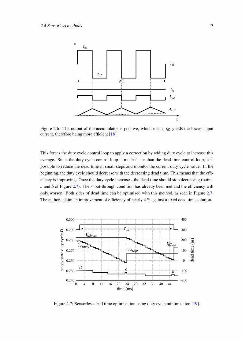
Yousefzadeh et al. [19] proposes another method of optimization of dead times without sens-
ing. The idea behind it is to optimize the efficiency by minimizing the duty cycle. For a given
load, there is an optimal duty cycle: when the dead times are too long (body diode conduction)
or too short (shoot-through current) the average value of the switching voltage 〈vS〉 is reduced.
2.4 Sensorless methods 13
t
td1
td2
tdi
Iout
Iin
Acc
NT
Figure 2.6: The output of the accumulator is positive, which means td2 yields the lowest inputcurrent, therefore being more efficient [18].
This forces the duty cycle control loop to apply a correction by adding duty cycle to increase this
average. Since the duty cycle control loop is much faster than the dead time control loop, it is
possible to reduce the dead time in small steps and monitor the current duty cycle value. In the
beginning, the duty cycle should decrease with the decreasing dead time. This means that the effi-
ciency is improving. Once the duty cycle increases, the dead time should stop decreasing (points
a and b of Figure 2.7). The shoot-through condition has already been met and the efficiency will
only worsen. Both sides of dead time can be optimized with this method, as seen in Figure 2.7.
The authors claim an improvement of efficiency of nearly 4 % against a fixed dead time solution.
stead
y s
tate
duty
cy
cle
D
0.300
0.290
0.280
0.270
0.260
0.250
0.2400 4 8 12 16 20 24 28 32 36 40 44
time (ms)
dead
tim
e (n
s)
400
300
200
100
0
-100
-200
ttot
td2max
td1maxtd1opt
td2opt
ab
D
Figure 2.7: Sensorless dead time optimization using duty cycle minimization [19].
14 Literature Review
Reiter et al. [20] proposes another method based on duty cycle monitoring. It is only suitable
for multiphase DC/DC converter, a typical automotive architecture. The algorithm introduces
a perturbation to the dead times in one phase of the converter and monitors the phase-currents
deviation. The most efficient phase is the one with the highest phase-current. A current-based
controller compensates this deviation by adjusting the duty cycles. The duty cycle difference
between phases allows the detection of the optimal dead times (similarly to [19]). This method
achieved an efficiency improvement of 1.40 %.
An interesting controller with incorporated dead time optimization is presented by Peterchev
et al. [21]. It is based on an extremum-seeking algorithm. Extremum-seeking control is a non-
model based real-time optimization approach used when only limited knowledge of the system
is available. In this paper, the controller introduces perturbations to the dead times and measures
the gradient of a cost function related to power efficiency (input current, temperature, duty cycle,
etc.).
2.5 Summary and discussion
A review of the literature related to the optimization of dead times on DC/DC converters has
been done. Each method presented has advantages and disadvantages, and it is not always easy
to compare them: each approach is tested in unequal conditions and compared with different
techniques (see Table 2.1). That said, the efficiency improvement values presented by each author
cannot be taken in an absolute manner – the conditions in which they are obtained must be analysed
if one wants to infer truthful comparisons.
The 5 % efficiency raise in Huang et al. [8] is mainly at light load conditions, when a width
controller is able to down size the integrated power MOSFETs. This is not available for larger
DC/DC converters made of discrete components. Despite the promising results, this method uses
complex circuitry which introduces some overhead.
Zhao et al. [14] is appropriate for applications with frequent load variations. However, it is
considerably more complex than other predictive methods, such as Mappus [10]. The latter case
displays a larger efficiency improvement than the first, because even though they both rank at
4 %, [14] is compared against a fixed dead time solution, while Mappus [10] is tested against an
adaptive method which, by itself, already improves over fixed dead time.
The results presented by Mei et al. [15] should be taken with caution, since they were not
produced under real testing conditions, but rather by simulation in PSIM. The benchmark was a
TPS2832, a synchronous buck converter MOSFET driver with adaptive dead time control. The IC
was modelled in PSIM with a fixed dead time of 15 ns, its minimal achievable delay.
The proposed sensorless methods have an overall worse performance than the switching volt-
age and current methods. They are also slower and thus not suitable for fast varying loads. But the
fact that no additional components are necessary to implement them, makes them a very attractive
option for digitally controlled DC/DC converters with minimal component overhead.
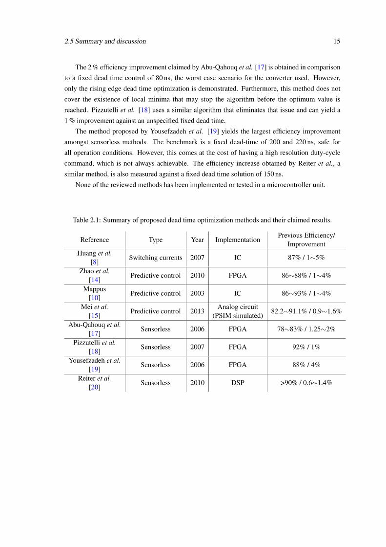
2.5 Summary and discussion 15
The 2 % efficiency improvement claimed by Abu-Qahouq et al. [17] is obtained in comparison
to a fixed dead time control of 80 ns, the worst case scenario for the converter used. However,
only the rising edge dead time optimization is demonstrated. Furthermore, this method does not
cover the existence of local minima that may stop the algorithm before the optimum value is
reached. Pizzutelli et al. [18] uses a similar algorithm that eliminates that issue and can yield a
1 % improvement against an unspecified fixed dead time.
The method proposed by Yousefzadeh et al. [19] yields the largest efficiency improvement
amongst sensorless methods. The benchmark is a fixed dead-time of 200 and 220 ns, safe for
all operation conditions. However, this comes at the cost of having a high resolution duty-cycle
command, which is not always achievable. The efficiency increase obtained by Reiter et al., a
similar method, is also measured against a fixed dead time solution of 150 ns.
None of the reviewed methods has been implemented or tested in a microcontroller unit.
Table 2.1: Summary of proposed dead time optimization methods and their claimed results.
Reference Type Year ImplementationPrevious Efficiency/
ImprovementHuang et al.
[8]Switching currents 2007 IC 87% / 1∼5%
Zhao et al.[14]
Predictive control 2010 FPGA 86∼88% / 1∼4%
Mappus[10]
Predictive control 2003 IC 86∼93% / 1∼4%
Mei et al.[15]
Predictive control 2013Analog circuit
(PSIM simulated)82.2∼91.1% / 0.9∼1.6%
Abu-Qahouq et al.[17]
Sensorless 2006 FPGA 78∼83% / 1.25∼2%
Pizzutelli et al.[18]
Sensorless 2007 FPGA 92% / 1%
Yousefzadeh et al.[19]
Sensorless 2006 FPGA 88% / 4%
Reiter et al.[20]
Sensorless 2010 DSP >90% / 0.6∼1.4%

16 Literature Review
Chapter 3
Analysis of Dead Time Optimization
Multiple variables influence the behavior of a synchronous buck converter in a complex way.
In this chapter a theoretical analysis of the processes behind dead time optimization is done. The
first section addresses the modeling of the algorithm, in mathematical terms. In the second section
the existence and consequences of certain system constraints is explored. The third section is about
the resources necessary in the digital controller responsible for running the algorithm. Lastly, in
the fourth section, an analysis of the power efficiency improvement is made and related to the
characteristics of the controller.
Since one of the objectives of this thesis is to implement a simple, computationally inexpensive
algorithm that takes advantage of the preexisting hardware for the elimination of dead time induced
power losses, the duty cycle minimizing approach reported by Yousefzadeh et al. [19] will be taken
as the starting point of this work. However, this does not impose any limitation to the analysis that
is made in this chapter.
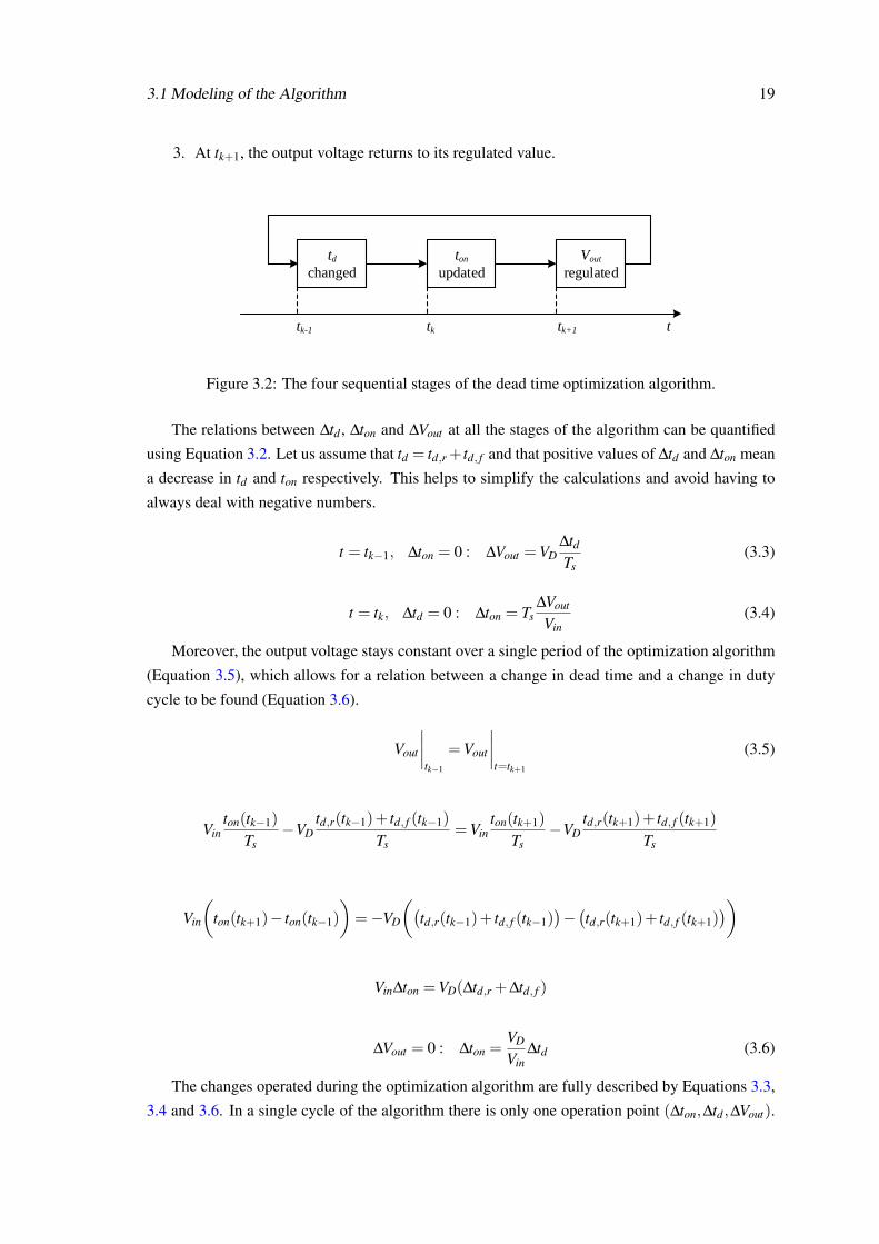
3.1 Modeling of the Algorithm
Switched mode converters are characterized for having a storage element that is sequentially
charged and discharged to provide controlled energy flow. In a synchronous buck converter, this
element is the inductor L. The average voltage across an inductor at steady state is null, which
implies that integrating the voltage across L over a single switching period Ts must equal 0. This
allows us to derive the output voltage as
∫ Ts
0VL dt = 0 (3.1)
∫td,r
VL dt +∫
ton
VL dt +∫
td, fVL dt +
∫to f f
VL dt = 0
∫td,r(−VD−Vout) dt +
∫ton
(Vin−Vout) dt +∫
td, f(−VD−Vout) dt +
∫to f f
−Vout dt = 0
17

18 Analysis of Dead Time Optimization
(−VD−Vout) td,r +(Vin−Vout) ton +(−VD−Vout) td, f −Vout (Ts− td,r− td, f ) = 0
Vout =Vinton
Ts−VD
td,r + td, fTs
(3.2)
where ton is the conduction time of the control switch, to f f is the conduction time of the syn-
chronous switch, and ton/Ts is the duty cycle. These quantities are depicted in Figure 1.2.
This mathematical relation1 can easily be given a physical significance: increasing the duty
cycle results in a higher output voltage, while increasing the dead time results in a lower output
voltage. In fact, the output voltage equals the average voltage at the switching node vsw (between
CS and SS) as seen in Figure 3.1.
+
--td,r td,f
˂vsw> = vout
˂vsw> = vout
Figure 3.1: The voltage at the switching node is either −VD or Vin. Its average equals the outputvoltage Vout .
Since the output voltage is regulated by the converter control loop, whatever this might be
composed of, any perturbation in the dead time has a direct impact on the duty cycle. This is
important for a sensorless, duty cycle minimizing algorithm for dead time optimization, such as
the one that is going to be used in this work. However this behavior is common to all converters
with a regulated output voltage. Considering the diagram of Figure 3.2, it is possible to describe
each stage in time as follows:
1. At tk−1, the dead time is changed (∆td), leading to a variation on the output voltage (∆Vout);
2. At tk, the controller detects the deviation ∆Vout and compensates by regulating the duty
cycle (∆ton);
1Equation 3.2 without the negative term is used for the case of an ideal converter, where the effects of the dead timeare not considered.
3.1 Modeling of the Algorithm 19
3. At tk+1, the output voltage returns to its regulated value.
td
changed
ton
updated
Vout
regulated
ttk-1 tk tk+1
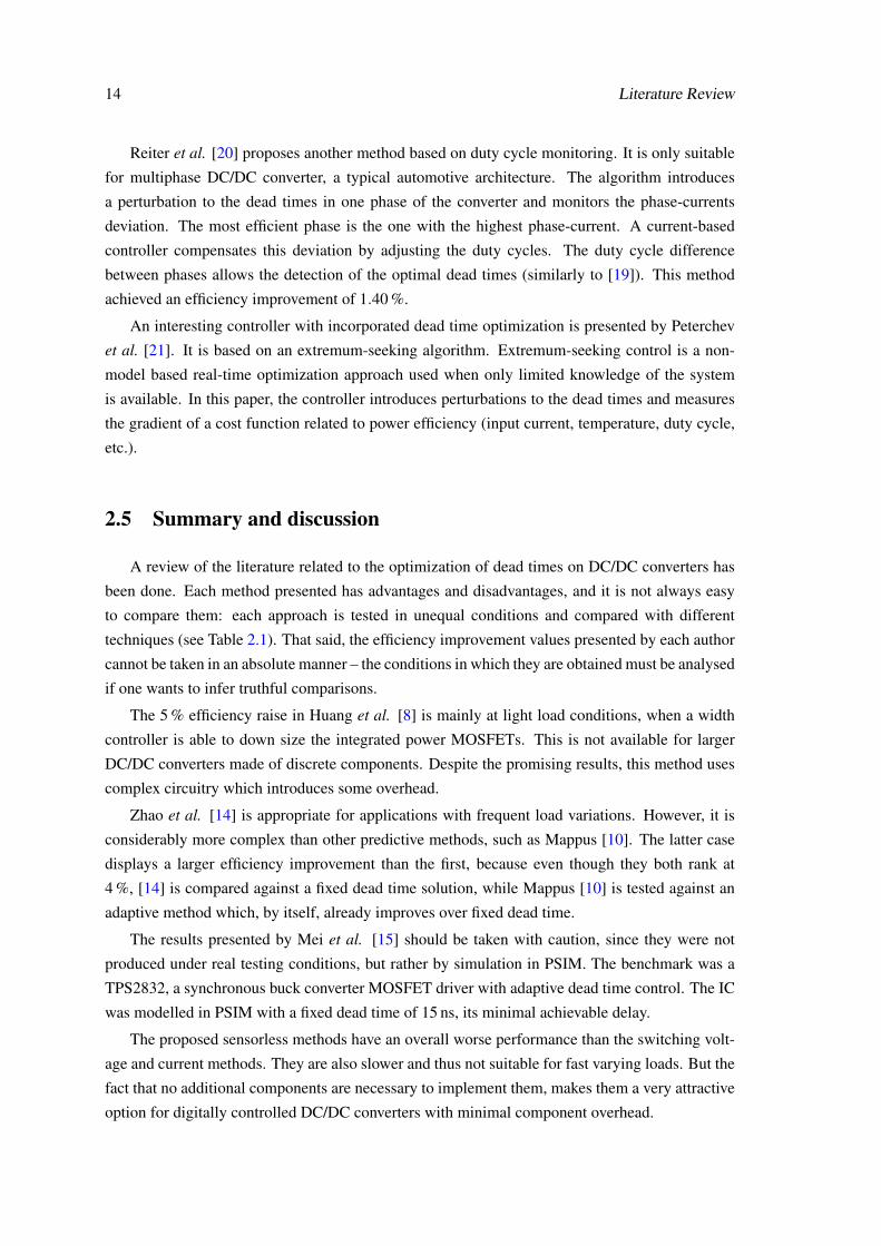
Figure 3.2: The four sequential stages of the dead time optimization algorithm.
The relations between ∆td , ∆ton and ∆Vout at all the stages of the algorithm can be quantified
using Equation 3.2. Let us assume that td = td,r + td, f and that positive values of ∆td and ∆ton mean
a decrease in td and ton respectively. This helps to simplify the calculations and avoid having to
always deal with negative numbers.
t = tk−1, ∆ton = 0 : ∆Vout =VD∆tdTs
(3.3)
t = tk, ∆td = 0 : ∆ton = Ts∆Vout
Vin(3.4)
Moreover, the output voltage stays constant over a single period of the optimization algorithm
(Equation 3.5), which allows for a relation between a change in dead time and a change in duty
cycle to be found (Equation 3.6).
Vout
∣∣∣∣tk−1
=Vout
∣∣∣∣t=tk+1
(3.5)
Vinton(tk−1)
Ts−VD
td,r(tk−1)+ td, f (tk−1)
Ts=Vin
ton(tk+1)
Ts−VD
td,r(tk+1)+ td, f (tk+1)
Ts
Vin
(ton(tk+1)− ton(tk−1)
)=−VD
((td,r(tk−1)+ td, f (tk−1)
)−(td,r(tk+1)+ td, f (tk+1)
))
Vin∆ton =VD(∆td,r +∆td, f )
∆Vout = 0 : ∆ton =VD
Vin∆td (3.6)
The changes operated during the optimization algorithm are fully described by Equations 3.3,
3.4 and 3.6. In a single cycle of the algorithm there is only one operation point (∆ton,∆td ,∆Vout).
20 Analysis of Dead Time Optimization
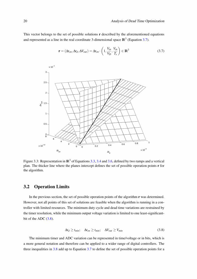
This vector belongs to the set of possible solutions r described by the aforementioned equations
and represented as a line in the real coordinate 3-dimensional space IR3 (Equation 3.7).
r = (∆ton,∆td ,∆Vout) = ∆ton ·(
1,Vin
VD,Vin
Ts
)∈ IR3 (3.7)
0 0.2 0.4 0.6 0.8 1
x 10−8
02
46
8
x 10−10
0
0.5
1
1.5
2
2.5
3
x 10−3
∆td
∆ton
∆vou
t
Figure 3.3: Representation in IR3 of Equations 3.3, 3.4 and 3.6, defined by two ramps and a verticalplan. The thicker line where the planes intercept defines the set of possible operation points r forthe algorithm.
3.2 Operation Limits
In the previous section, the set of possible operation points of the algorithm r was determined.
However, not all points of this set of solutions are feasible when the algorithm is running in a con-
troller with limited resources. The minimum duty cycle and dead time variations are restrained by
the timer resolution, while the minimum output voltage variation is limited to one least-significant-
bit of the ADC (3.8).
∆td ≥ tmin; ∆ton ≥ tmin; ∆Vout ≥Vmin (3.8)
The minimum timer and ADC variation can be represented in time/voltage or in bits, which is
a more general notation and therefore can be applied to a wider range of digital controllers. The
three inequalities in 3.8 add up to Equation 3.7 to define the set of possible operation points for a
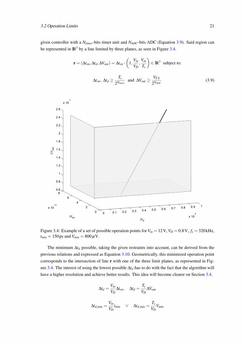
3.2 Operation Limits 21
given controller with a Ntimer-bits timer unit and NADC-bits ADC (Equation 3.9). Said region can
be represented in IR3 by a line limited by three planes, as seen in Figure 3.4.
r = (∆ton,∆td ,∆Vout) = ∆ton ·(
1,Vin
VD,Vin
Ts
)∈ IR3 subject to:
∆ton, ∆td ≥Ts
2Ntimerand ∆Vout ≥
VFS
2NADC(3.9)
Figure 3.4: Example of a set of possible operation points for Vin = 12V, VD = 0.8V, fs = 320kHz,tmin = 150ps and Vmin = 800 µV.
The minimum ∆td possible, taking the given restraints into account, can be derived from the
previous relations and expressed as Equation 3.10. Geometrically, this minimized operation point
corresponds to the intersection of line r with one of the three limit planes, as represented in Fig-
ure 3.4. The interest of using the lowest possible ∆td has to do with the fact that the algorithm will
have a higher resolution and achieve better results. This idea will become clearer on Section 3.4.
∆td =Vin
VD∆ton, ∆td =
Ts
VD∆Vout
∆td,min =Vin
VDtmin ∨ ∆td,min =
Ts
VDVmin
22 Analysis of Dead Time Optimization
∆td,min =Vin
VD
Ts
2Ntimer∨ ∆td,min =
Ts
VD
VFS
2NADC
∆td,min = max
Vin
VD
Ts
2Ntimer,
Ts
VD
VFS
2NADC
∆td,min = TsVin
VDmax
2−Ntimer ,
VFS
Vin2−NADC
(3.10)
At Equation 3.10 the maximum value is used for calculating ∆td,min because choosing the
minimum would imply that one of the other two variables ∆ton or ∆Vout would be smaller than tmin
or Vmin and violate the restraints imposed by the system.
3.3 Resource Usage
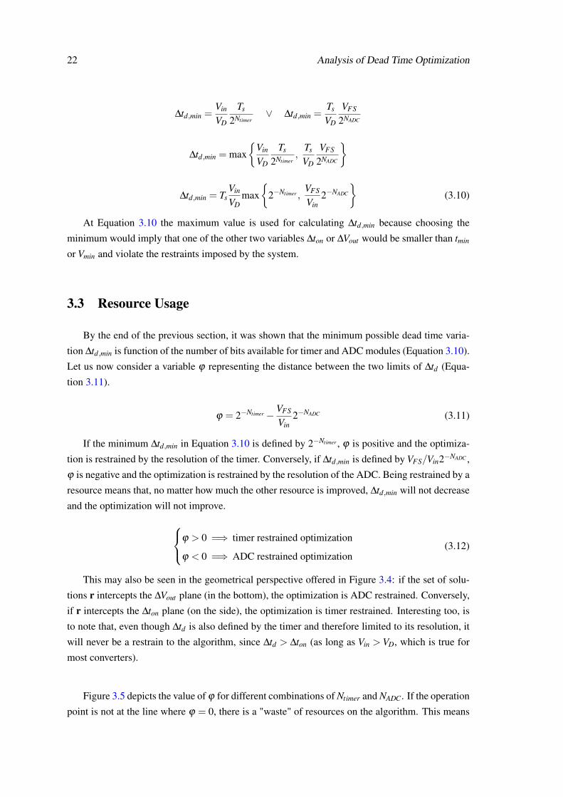
By the end of the previous section, it was shown that the minimum possible dead time varia-
tion ∆td,min is function of the number of bits available for timer and ADC modules (Equation 3.10).
Let us now consider a variable ϕ representing the distance between the two limits of ∆td (Equa-
tion 3.11).
ϕ = 2−Ntimer − VFS
Vin2−NADC (3.11)
If the minimum ∆td,min in Equation 3.10 is defined by 2−Ntimer , ϕ is positive and the optimiza-
tion is restrained by the resolution of the timer. Conversely, if ∆td,min is defined by VFS/Vin2−NADC ,
ϕ is negative and the optimization is restrained by the resolution of the ADC. Being restrained by a
resource means that, no matter how much the other resource is improved, ∆td,min will not decrease
and the optimization will not improve.ϕ > 0 =⇒ timer restrained optimization
ϕ < 0 =⇒ ADC restrained optimization(3.12)
This may also be seen in the geometrical perspective offered in Figure 3.4: if the set of solu-
tions r intercepts the ∆Vout plane (in the bottom), the optimization is ADC restrained. Conversely,
if r intercepts the ∆ton plane (on the side), the optimization is timer restrained. Interesting too, is
to note that, even though ∆td is also defined by the timer and therefore limited to its resolution, it
will never be a restrain to the algorithm, since ∆td > ∆ton (as long as Vin > VD, which is true for
most converters).
Figure 3.5 depicts the value of ϕ for different combinations of Ntimer and NADC. If the operation
point is not at the line where ϕ = 0, there is a "waste" of resources on the algorithm. This means
3.4 Power Efficiency Improvement 23
that either the timer or the ADC use excessive bits that are not contributing to the optimization.
That said, the resource usage is optimal for
Ntimer = NADC + log2
(Vin
VFS
)(3.13)
If a certain operation point where ϕ = |ϕi| is moved to a point where ϕ =∣∣ϕ f∣∣< |ϕi|, the re-
source usage is improved. However, this does not guarantee that the power efficiency will improve.
Over the next section this will be explained further.
-0.06 -0.06-0.05 -0.05-0.04
-0.04 -0.04-0.03
-0.03 -0.03-0.0
2
-0.02 -0.02
-0.01
-0.01 -0.01
0
0
0
0
0.01
0.01
0.01
0.02
0.02
0.02
0.03
0.03
0.03
0.04
0.04
0.04
0.05
0.05
0.05
0.06
0.06
0.06
0.07
0.07
0.07
0.08
0.08
0.08
0.09
0.09
0.09
0.1
0.1
0.1
Ntimer
NADC
2 4 6 8 10 12 14 162
4
6
8
10
12
14
16
Figure 3.5: Dependency of ϕ on timer (Ntimer) and ADC resolution (NADC) for Vin = 12V, VD =0.8V, fs = 320kHz and VFS = 3.3V.
3.4 Power Efficiency Improvement
In Chapter 1 the problem of dead time, diodes and power losses has already been mentioned:
asynchronous buck converters lose energy through the freewheel diode during the entire to f f time,
while synchronous buck converters partially resolve this by replacing the diode with a MOSFET.
However, the body diode of the synchronous switch still conducts for td . Despite being signifi-
cantly lower than in the asynchronous counterpart, the diode losses of the synchronous converter
still weight in the total converter efficiency.
The dominant part of the losses on a diode comes from conduction. Conduction losses are
directly proportional to the diode conduction time, or as it is most commonly called, the dead time
(Equation 3.14). Additionally, the body diode suffers from reverse recovery losses. For a diode to
24 Analysis of Dead Time Optimization
transition from conducting to blocking state, the charge distribution must change. This movement
of the free carriers does not occur instantaneously, so during this short period of time, known
as reverse recovery time, the diode will not block and, therefore, temporarily conduct a large
current in the reverse direction [22]. The losses produced by this non-ideality are represented by
Equation 3.15.
PD,cond =VDIout fs(td,r + td, f ) (3.14)
PD,RR =12
QRRVins fs (3.15)
Another source of losses due to the existence of dead time is the increase of conduction time
of the control switch, in order to maintain the same output voltage, as represented in Equation 3.6.
However, these losses are in the order of nW compared to the hundreds of mW of the conduction
losses and will not be taken into account. The reverse recovery losses are also considerably smaller
than the conduction losses, about 100 times less. Furthermore, they are constantly present, unless
the diode is not at all forward-biased to begin with. Therefore, from now on the total diode losses
will be approximated by the conduction losses only.
Ploss ≈VDIout fstd
We are now in conditions to quantify how much the power losses in the body diode change
when there is a variation in the dead time. In the previous section of this chapter, the mini-
mum dead time variation ∆td,min for a system with certain characteristics was determined (Equa-
tion 3.10). This is the dead time variation that also produces the minimum power loss variation.
∆Ploss,min =VDIout fs∆td,min (3.16)
Let us consider an initial (fixed) dead time td,i that causes a certain amount of initial power
losses Ploss,i. Since the minimum dead time decrement is given by ∆td,min, and such variation
reduces the power losses in ∆Ploss,min, it is possible to determine how much from the initial losses
can be eliminated with a given algorithm operation point. Let Ψ be the efficiency improvement
factor, a relation between eliminated losses Ploss,elim and total initial losses Ploss,i.
Ψ =Ploss,elim
Ploss,i(3.17)
The algorithm will reduce the dead time in steps of ∆td,min, subtracting with each step ∆Ploss,min
from the total losses Ploss,i. This means that Ploss,elim = bγc ·∆Ploss,min where bγc is the integer
number of steps that is possible to take towards null losses. Hence, Ψ can be expressed as
Ψ =b Ploss,i
∆Ploss,minc∆Ploss,min
Ploss,i(3.18)
3.4 Power Efficiency Improvement 25
As explained before, γ is the ideal number of steps that are necessary to achieve total loss
elimination. In practice however, steps can only be integer, which allows Equation 3.20 to be
formulated, by replacing in Equation 3.18.
Ploss,elim = bγc ·∆Ploss,min
Ploss,i = γ ·∆Ploss,min
γ =Ploss,i
∆Ploss,min=
VDIout fstd,iVDIout fs∆td,min
=td,i
∆td,min(3.19)
Ψ =bγcγ
(3.20)
Ψ can be depicted as a function of γ , as seen in Figure 3.6a. Notice that when γ is an integer,
even at small values, the losses are fully eliminated. However, this only happens at very precise
points: if γ suffers the slighest variation, the improvement will drop significantly. To overcome
this, the floor function b·c may be approximated by bxc = x− 12 +
1π
∑∞k=1
sin(2πkx)k ≈ x− 1
2 and
Equation 3.20 ends up being represented as Equation 3.21. Figure 3.6b depicts the approximated,
averaged relation of γ with Ψ which better describes what happens in reality than Figure 3.6a.
Ψ = 1−∆Ploss,min
2Ploss,i= 1−
∆td,min
2td,i(3.21)
0 2 4 6 8 10 12 14 16 18 200
10
20
30
40
50
60
70
80
90
100
(a)
0 2 4 6 8 10 12 14 16 18 200
10
20
30
40
50
60
70
80
90
100
(b)
Figure 3.6: Depictions of Ψ(γ): (a) Using the theoretical bγc , (b) using the floor function approx-imation that better models the real variations of γ .
A small value of γ means a large initial dead time td,i or a large step ∆td,min , which is caused by
having a low resolution at either the timer or the ADC. Conversely, a large γ means a small ∆td,min
or a small td,i, which is the direct consequence of having a high resolution at both resources.
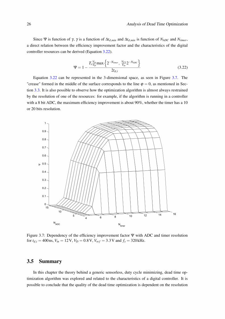
26 Analysis of Dead Time Optimization
Since Ψ is function of γ , γ is a function of ∆td,min and ∆td,min is function of NADC and Ntimer,
a direct relation between the efficiency improvement factor and the characteristics of the digital
controller resources can be derived (Equation 3.22).
Ψ = 1−Ts
VinVD
max
2−Ntimer , VFSVin
2−NADC
2td,i
(3.22)
Equation 3.22 can be represented in the 3-dimensional space, as seen in Figure 3.7. The
"crease" formed in the middle of the surface corresponds to the line ϕ = 0, as mentioned in Sec-
tion 3.3. It is also possible to observe how the optimization algorithm is almost always restrained
by the resolution of one of the resources: for example, if the algorithm is running in a controller
with a 8 bit ADC, the maximum efficiency improvement is about 90%, whether the timer has a 10
or 20 bits resolution.
4 6 8 10 12 14 165
10
150
0.1
0.2
0.3
0.4
0.5
0.6
0.7
0.8
0.9
1
Ntimer
NADC
Figure 3.7: Dependency of the efficiency improvement factor Ψ with ADC and timer resolutionfor td,i = 400ns, Vin = 12V, VD = 0.8V, Vre f = 3.3V and fs = 320kHz.
3.5 Summary
In this chapter the theory behind a generic sensorless, duty cycle minimizing, dead time op-
timization algorithm was explored and related to the characteristics of a digital controller. It is
possible to conclude that the quality of the dead time optimization is dependent on the resolution

3.5 Summary 27
of timer and ADC and that these two are also related between each other: the resolution of one
of the resources may restrain the optimization, no matter how good the resolution of the non-
restraining resource is. Since the algorithm is theoretically proved, the next chapter will present a
practical implementation and relate its results with the theory.

28 Analysis of Dead Time Optimization

Chapter 4
Experimental Results
In the previous chapter, the theory behind the optimization of dead time related losses using
a duty cycle minimizing algorithm was presented. Now a concrete application of an algorithm of
this kind is presented. In the first section, the hardware and its relevant capabilities are explored
as well as the experimental setup used in this work. Next the software is presented, consisting of
the voltage control law, the dead time algorithm and its coding. The third section consists of the
performed measurements and their relation with the previously expected results. Lastly, the fourth
section presents a simulation in Simulink and the extracted data.
4.1 Powertrain and Microcontroller Unit
The most important part of the hardware is the buck converter and the microcontroller. In this
work Infineon synchronous buck converter kit with a control card was used as the proof-of-concept
prototype. This kit has two channels and is controlled by a detachable card containing an ARM-
Cortex M4 based XMC4200 microcontroller [4] and on-board Segger J-Link debugger. The most
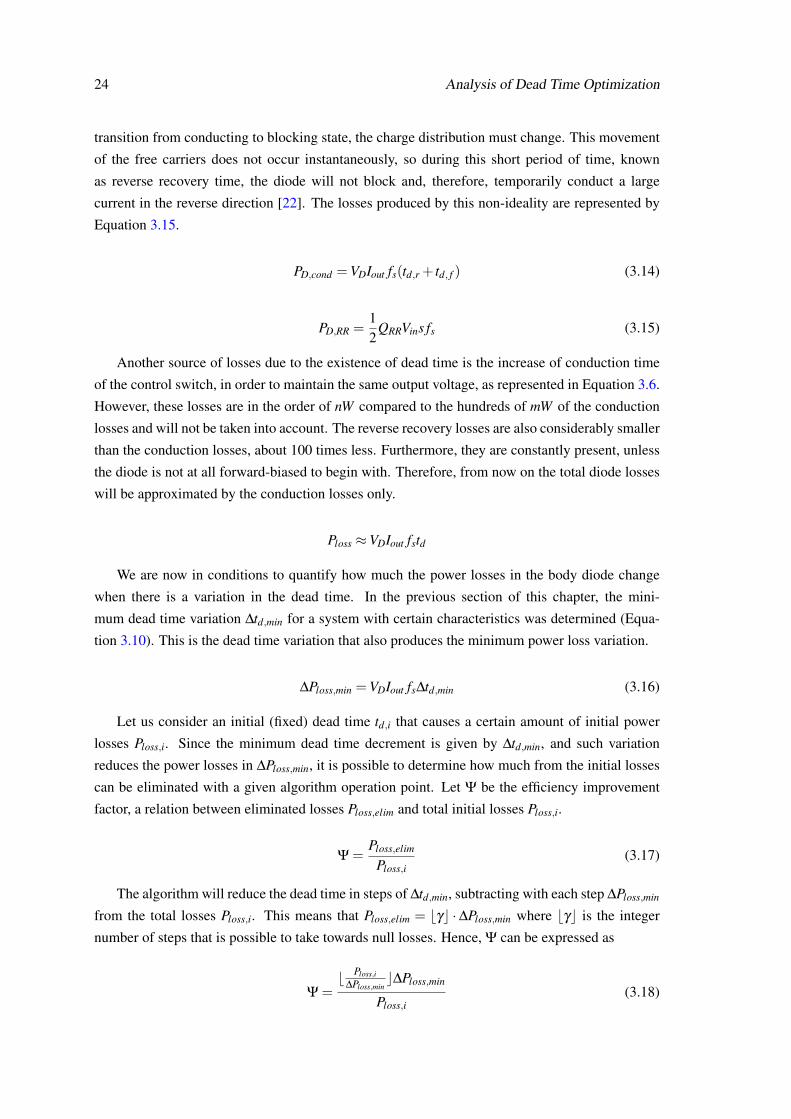
important parameters and components of the converter and control card are listed on Table 4.1.
Figure 4.1 shows the main features of the buck converter kit and the control card, as well as how
the assembled setup looks like.
Table 4.1: Operation parameters for the prototype buck converter.
Parameter ValueVin 12 V
Vout,nom 1.8 VIout,max 5 APout,max 9 W
L 33 µHC 330 µFfs 320 kHz
29
30 Experimental Results
12V DC Power Supply Connector
Control Card Connector
Buck Converter 0
Buck Converter 1 Network Analysis
Probe Points
Load Connector
Step Load
Switch
Micro USB
Isolator
Control Card Connector
Power-On LED
XMC4200
On-Board COM and
Segger J-Link debugger
Figure 4.1: The proof-of-concept prototype: buck converter kit and XMC4200 control card.
The load selected is a 0.5 Ω, 15 W power resistor. However, the step load switch also gives
the possibility to transition from and to no-load conditions instantaneously. This will be useful for
testing load variations, as explained further in this chapter.
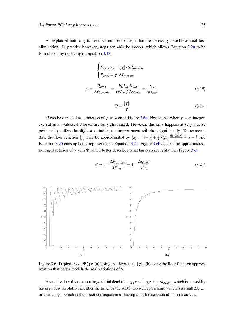
The XMC4200 features several peripherals that are relevant for this kind of application, such
as the Interrupt Controller (NVIC), Input/Outputs (GPIO) and the Analog-to-Digital Controller
(VADC). An overview of all the used peripherals in this application is depicted in Figure 4.2.
Figure 4.2: A view of the microcontroller peripherals required by the project.
The most important for this work is, however, the High Resolution PWM and the Timer,
which is called Capture and Compare Unit (CCU8) in this microcontroller family. The HRPWM
4.1 Powertrain and Microcontroller Unit 31
is a peripheral that consists of a Compare and Slope Generator (CSG) for peak current control,
slope compensation, clamping, blanking, etc., and a High Resolution Channel (HRC) which can
adjust the edges of its input signal by very small steps in the order of picoseconds. The CCU8
(12.5 ns resolution) generates a low resolution PWM waveform which enters the HRPWM (150 ps
resolution), is fine adjusted and then can be output to a pin, as a high-resolution PWM waveform
(as depicted in Figure 4.5 of the next section). Later, there will be an explanation on how the
HRPWM is programmed and used.
Using HRPWM for a dead time optimization algorithm is interesting for two reasons: not
only the minimum dead time step ∆td,min can be smaller and hence the efficiency improvement
factor Ψ increases, but also because the control loop can vary the duty cycle in a much finer way,
leading to smaller ∆ton values. For an algorithm that uses the duty cycle as a minimization variable,
increasing the resolution of the duty cycle is a clear advantage.
The power efficiency of the converter can be expressed as
µ =Pout
Pin=
Vout · Iout
Vin · Iin(4.1)
Since the load is constant and known in this experimental setup and the output and input
voltages are fixed and constant, only the input current is missing in order to calculate the absolute
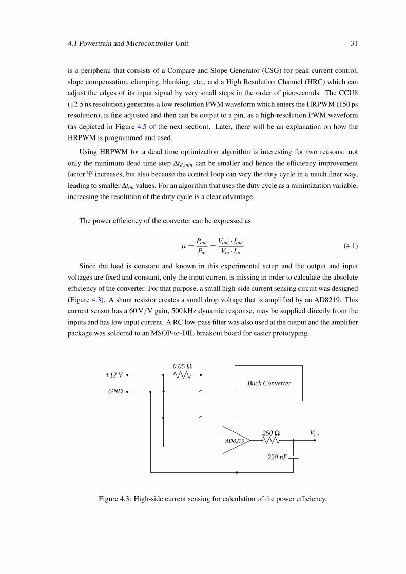
efficiency of the converter. For that purpose, a small high-side current sensing circuit was designed
(Figure 4.3). A shunt resistor creates a small drop voltage that is amplified by an AD8219. This
current sensor has a 60 V/V gain, 500 kHz dynamic response, may be supplied directly from the
inputs and has low input current. A RC low-pass filter was also used at the output and the amplifier
package was soldered to an MSOP-to-DIL breakout board for easier prototyping.
Buck Converter
+12 V
GND
0.05
250
220 nF
VIin
AD8219
Figure 4.3: High-side current sensing for calculation of the power efficiency.
32 Experimental Results
4.2 Software and Algorithm
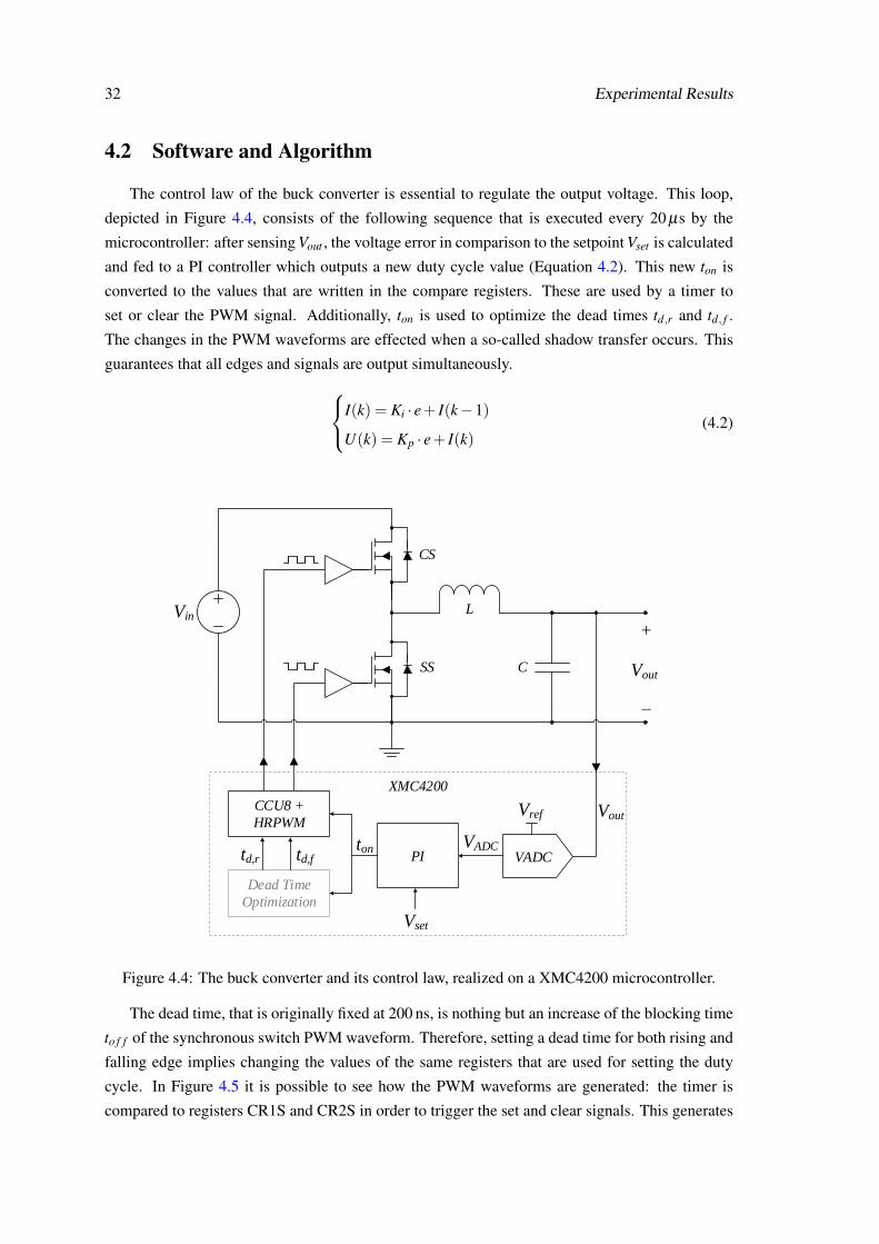
The control law of the buck converter is essential to regulate the output voltage. This loop,
depicted in Figure 4.4, consists of the following sequence that is executed every 20 µs by the
microcontroller: after sensing Vout , the voltage error in comparison to the setpoint Vset is calculated
and fed to a PI controller which outputs a new duty cycle value (Equation 4.2). This new ton is
converted to the values that are written in the compare registers. These are used by a timer to
set or clear the PWM signal. Additionally, ton is used to optimize the dead times td,r and td, f .
The changes in the PWM waveforms are effected when a so-called shadow transfer occurs. This
guarantees that all edges and signals are output simultaneously.I(k) = Ki · e+ I(k−1)
U(k) = Kp · e+ I(k)(4.2)
CS
SS
VinL
C Vout
+
VADCPI
ton
CCU8 +
HRPWM
Dead Time
Optimization
td,r td,f
XMC4200
Vout
Vset
VADC
Vref
Figure 4.4: The buck converter and its control law, realized on a XMC4200 microcontroller.
The dead time, that is originally fixed at 200 ns, is nothing but an increase of the blocking time
to f f of the synchronous switch PWM waveform. Therefore, setting a dead time for both rising and
falling edge implies changing the values of the same registers that are used for setting the duty
cycle. In Figure 4.5 it is possible to see how the PWM waveforms are generated: the timer is
compared to registers CR1S and CR2S in order to trigger the set and clear signals. This generates
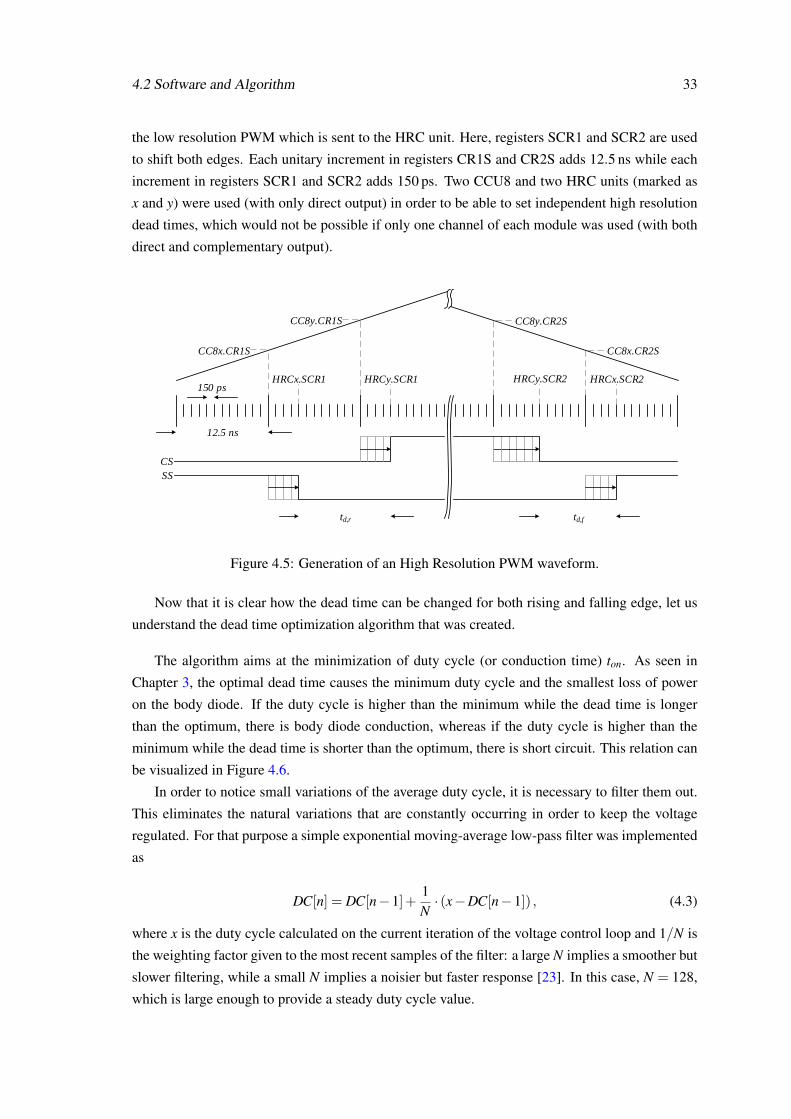
4.2 Software and Algorithm 33
the low resolution PWM which is sent to the HRC unit. Here, registers SCR1 and SCR2 are used
to shift both edges. Each unitary increment in registers CR1S and CR2S adds 12.5 ns while each
increment in registers SCR1 and SCR2 adds 150 ps. Two CCU8 and two HRC units (marked as
x and y) were used (with only direct output) in order to be able to set independent high resolution
dead times, which would not be possible if only one channel of each module was used (with both
direct and complementary output).
CC8y.CR2S
HRCy.SCR2HRCx.SCR1
CC8x.CR1S
HRCy.SCR1
CC8y.CR1S
CC8x.CR2S
12.5 ns
150 psHRCx.SCR2
td,r td,f
CS
SS
Figure 4.5: Generation of an High Resolution PWM waveform.
Now that it is clear how the dead time can be changed for both rising and falling edge, let us
understand the dead time optimization algorithm that was created.
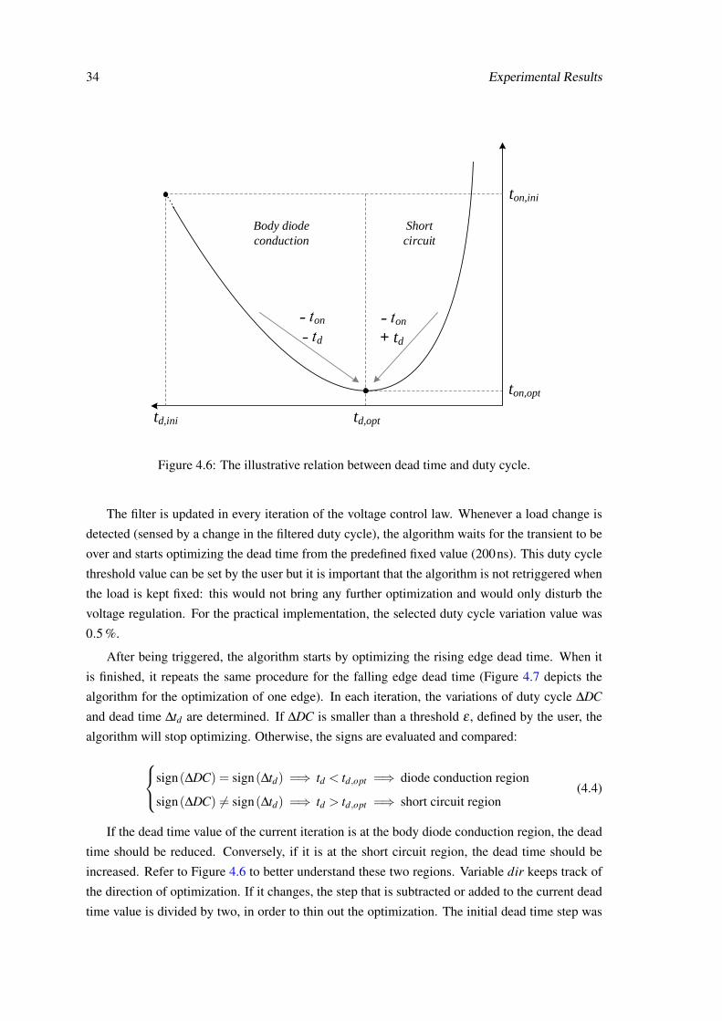
The algorithm aims at the minimization of duty cycle (or conduction time) ton. As seen in
Chapter 3, the optimal dead time causes the minimum duty cycle and the smallest loss of power
on the body diode. If the duty cycle is higher than the minimum while the dead time is longer
than the optimum, there is body diode conduction, whereas if the duty cycle is higher than the
minimum while the dead time is shorter than the optimum, there is short circuit. This relation can
be visualized in Figure 4.6.
In order to notice small variations of the average duty cycle, it is necessary to filter them out.
This eliminates the natural variations that are constantly occurring in order to keep the voltage
regulated. For that purpose a simple exponential moving-average low-pass filter was implemented
as
DC[n] = DC[n−1]+1N· (x−DC[n−1]) , (4.3)
where x is the duty cycle calculated on the current iteration of the voltage control loop and 1/N is
the weighting factor given to the most recent samples of the filter: a large N implies a smoother but
slower filtering, while a small N implies a noisier but faster response [23]. In this case, N = 128,
which is large enough to provide a steady duty cycle value.
34 Experimental Results
td,opttd,ini
ton,opt
˗ ton
˗ td
˗ ton
+ td
ton,ini
Body diode
conduction
Short
circuit
Figure 4.6: The illustrative relation between dead time and duty cycle.
The filter is updated in every iteration of the voltage control law. Whenever a load change is
detected (sensed by a change in the filtered duty cycle), the algorithm waits for the transient to be
over and starts optimizing the dead time from the predefined fixed value (200ns). This duty cycle
threshold value can be set by the user but it is important that the algorithm is not retriggered when
the load is kept fixed: this would not bring any further optimization and would only disturb the
voltage regulation. For the practical implementation, the selected duty cycle variation value was
0.5 %.
After being triggered, the algorithm starts by optimizing the rising edge dead time. When it
is finished, it repeats the same procedure for the falling edge dead time (Figure 4.7 depicts the
algorithm for the optimization of one edge). In each iteration, the variations of duty cycle ∆DC
and dead time ∆td are determined. If ∆DC is smaller than a threshold ε , defined by the user, the
algorithm will stop optimizing. Otherwise, the signs are evaluated and compared:sign(∆DC) = sign(∆td) =⇒ td < td,opt =⇒ diode conduction region
sign(∆DC) 6= sign(∆td) =⇒ td > td,opt =⇒ short circuit region(4.4)
If the dead time value of the current iteration is at the body diode conduction region, the dead
time should be reduced. Conversely, if it is at the short circuit region, the dead time should be
increased. Refer to Figure 4.6 to better understand these two regions. Variable dir keeps track of
the direction of optimization. If it changes, the step that is subtracted or added to the current dead
time value is divided by two, in order to thin out the optimization. The initial dead time step was
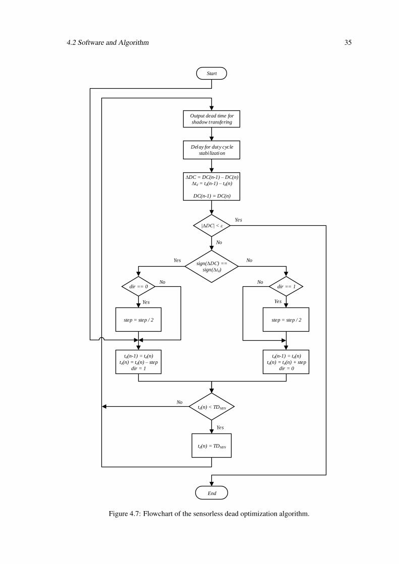
4.2 Software and Algorithm 35
Start
Delay for duty cycle
stabilization
sign(∆DC) ==
sign(∆td)
∆DC = DC(n-1) – DC(n)
∆td = td(n-1) – td(n)
DC(n-1) = DC(n)
|∆DC| < ε
td(n-1) = td(n)
td(n) = td(n) – step
dir = 1
td(n-1) = td(n)
td(n) = td(n) + step
dir = 0
td(n) < TDMIN
dir == 0 dir == 1
step = step / 2 step = step / 2
td(n) = TDMIN
No
NoYes
Yes Yes
Yes
End
Yes
No No
No
Output dead time for
shadow transfering
Figure 4.7: Flowchart of the sensorless dead optimization algorithm.

36 Experimental Results
set to 25 ns but it can be changed for other applications. The duty cycle value varies similarly to
a ball falling in a round container, bouncing left and right reaching smaller and smaller heights,
until it stops at the bottom.
An interesting side note is to understand that ε , the minimum duty cycle variation in order to
keep the algorithm running, is equal to the minimum possible duty cycle variation ∆ton,min, derived
in Section 3.2.
Another feature is the existence of a user defined minimum dead time. This prevents that
when the step is still large (has not been divided yet), the dead time is set to a value well inside the
short circuit region, guaranteeing the integrity of the hardware. For this specific application, the
minimum was set at 25 ns, slightly into the short circuit operation region.
After an iteration of the algorithm is finished and the current dead time is selected, the delay
is armed, the program returns to the control routine and shadow transfers the values of duty cycle
and dead time in the registers. The optimization algorithm is only resumed after a certain number
of control loop executions, when the delay is over, in order to allow the duty cycle to settle and the
filter to obtain the new average value.
4.3 Measurements and Results
The platform that was used to write the code, configure the peripherals, program the micro-
controller and debug the project was DAVE3, the integrated development environment for XMC
microcontrollers by Infineon Technologies. One of the most useful and interesting features is
called xSPY, a plug-in that enables users to visualize data in real time and create graphic inter-
faces to control and interact with the running application. It is also possible to export data for
.csv files in order to plot variables in MATLAB. xSPY was the way that most measurements were
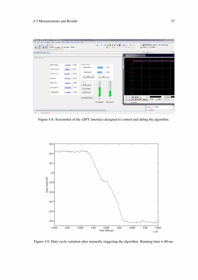
produced. Figure 4.8 shows the used interface while the converter is running. It is possible to use
a virtual oscilloscope to watch the duty cycle and log the data, as well as manually set dead time
values and trigger the optimization algorithm.
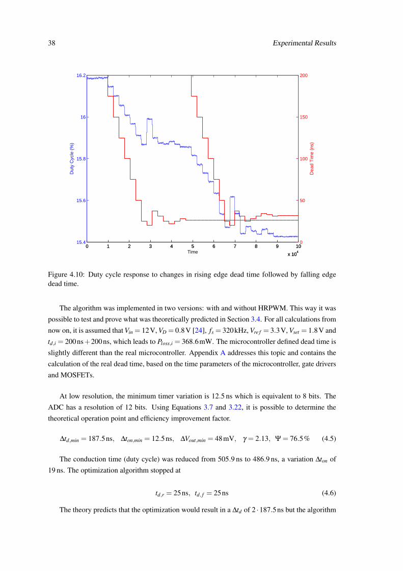
With the help of this plug-in it was possible to measure how quick the algorithm is. In Fig-
ure 4.9, every unity in the time domain corresponds to 500 µs, the streaming frequency of xSPY.
This means that the whole optimization takes roughly 80 ms. It is also possible to observe in the
middle and end of the optimization how the algorithm slows down. This corresponds to the time
when the minimum dead times are being searched more finely. In Figure 4.10 it is possible to
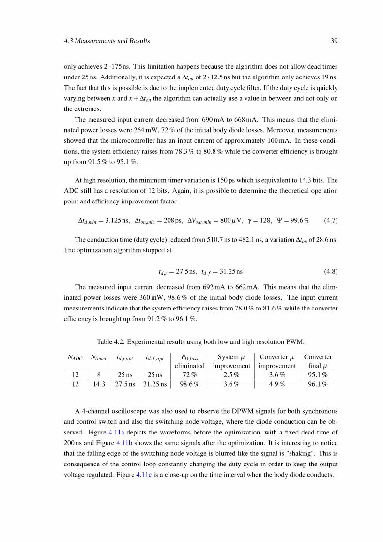
observe a very slow run of the optimization algorithm. The blue line corresponds to the duty cycle
while the red represents first the rising edge dead time and second the falling edge dead time. It
is interesting to notice that the peaks of duty cycle, corresponding to when the dead time is inside
the short circuit region, are small. This demonstrates how the safety of the powertrain is kept at
all times by only allowing the dead time to "probe" the short circuit region. At full speed, these
peaks are even shorter and the hardware is not compromised.
4.3 Measurements and Results 37
Figure 4.8: Screenshot of the xSPY interface designed to control and debug the algorithm.
4.815 4.82 4.825 4.83 4.835 4.84 4.845 4.85 4.855
x 104
15.5
15.6
15.7
15.8
15.9
16
16.1
16.2
16.3
Time (500 µs)
Dut
y C
ycle
(%
)
Figure 4.9: Duty cycle variation after manually triggering the algorithm. Running time is 80 ms.
38 Experimental Results
0 1 2 3 4 5 6 7 8 9 10
x 104
15.4
15.6
15.8
16
16.2
Time
Dut
y C
ycle
(%
)
0 1 2 3 4 5 6 7 8 9 10
x 104
0
50
100
150
200
Dea
d T
ime
(ns)
Figure 4.10: Duty cycle response to changes in rising edge dead time followed by falling edgedead time.
The algorithm was implemented in two versions: with and without HRPWM. This way it was
possible to test and prove what was theoretically predicted in Section 3.4. For all calculations from
now on, it is assumed that Vin = 12V, VD = 0.8V [24], fs = 320kHz, Vre f = 3.3V, Vset = 1.8V and
td,i = 200ns+200ns, which leads to Ploss,i = 368.6mW. The microcontroller defined dead time is
slightly different than the real microcontroller. Appendix A addresses this topic and contains the
calculation of the real dead time, based on the time parameters of the microcontroller, gate drivers
and MOSFETs.
At low resolution, the minimum timer variation is 12.5 ns which is equivalent to 8 bits. The
ADC has a resolution of 12 bits. Using Equations 3.7 and 3.22, it is possible to determine the
theoretical operation point and efficiency improvement factor.
∆td,min = 187.5ns, ∆ton,min = 12.5ns, ∆Vout,min = 48mV, γ = 2.13, Ψ = 76.5% (4.5)
The conduction time (duty cycle) was reduced from 505.9 ns to 486.9 ns, a variation ∆ton of
19 ns. The optimization algorithm stopped at
td,r = 25ns, td, f = 25ns (4.6)
The theory predicts that the optimization would result in a ∆td of 2 ·187.5ns but the algorithm
4.3 Measurements and Results 39
only achieves 2 ·175ns. This limitation happens because the algorithm does not allow dead times
under 25 ns. Additionally, it is expected a ∆ton of 2 ·12.5ns but the algorithm only achieves 19 ns.
The fact that this is possible is due to the implemented duty cycle filter. If the duty cycle is quickly
varying between x and x+∆ton the algorithm can actually use a value in between and not only on
the extremes.
The measured input current decreased from 690 mA to 668 mA. This means that the elimi-
nated power losses were 264 mW, 72 % of the initial body diode losses. Moreover, measurements
showed that the microcontroller has an input current of approximately 100 mA. In these condi-
tions, the system efficiency raises from 78.3 % to 80.8 % while the converter efficiency is brought
up from 91.5 % to 95.1 %.
At high resolution, the minimum timer variation is 150 ps which is equivalent to 14.3 bits. The
ADC still has a resolution of 12 bits. Again, it is possible to determine the theoretical operation
point and efficiency improvement factor.
∆td,min = 3.125ns, ∆ton,min = 208ps, ∆Vout,min = 800 µV, γ = 128, Ψ = 99.6% (4.7)
The conduction time (duty cycle) reduced from 510.7 ns to 482.1 ns, a variation ∆ton of 28.6 ns.
The optimization algorithm stopped at
td,r = 27.5ns, td, f = 31.25ns (4.8)
The measured input current decreased from 692 mA to 662 mA. This means that the elim-
inated power losses were 360 mW, 98.6 % of the initial body diode losses. The input current
measurements indicate that the system efficiency raises from 78.0 % to 81.6 % while the converter
efficiency is brought up from 91.2 % to 96.1 %.
Table 4.2: Experimental results using both low and high resolution PWM.
NADC Ntimer td,r,opt td, f ,opt PD,loss System µ Converter µ Convertereliminated improvement improvement final µ
12 8 25 ns 25 ns 72 % 2.5 % 3.6 % 95.1 %12 14.3 27.5 ns 31.25 ns 98.6 % 3.6 % 4.9 % 96.1 %
A 4-channel oscilloscope was also used to observe the DPWM signals for both synchronous
and control switch and also the switching node voltage, where the diode conduction can be ob-
served. Figure 4.11a depicts the waveforms before the optimization, with a fixed dead time of
200 ns and Figure 4.11b shows the same signals after the optimization. It is interesting to notice
that the falling edge of the switching node voltage is blurred like the signal is "shaking". This is
consequence of the control loop constantly changing the duty cycle in order to keep the output
voltage regulated. Figure 4.11c is a close-up on the time interval when the body diode conducts.
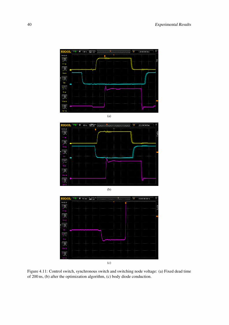
40 Experimental Results
(a)
(b)
(c)
Figure 4.11: Control switch, synchronous switch and switching node voltage: (a) Fixed dead timeof 200 ns, (b) after the optimization algorithm, (c) body diode conduction.
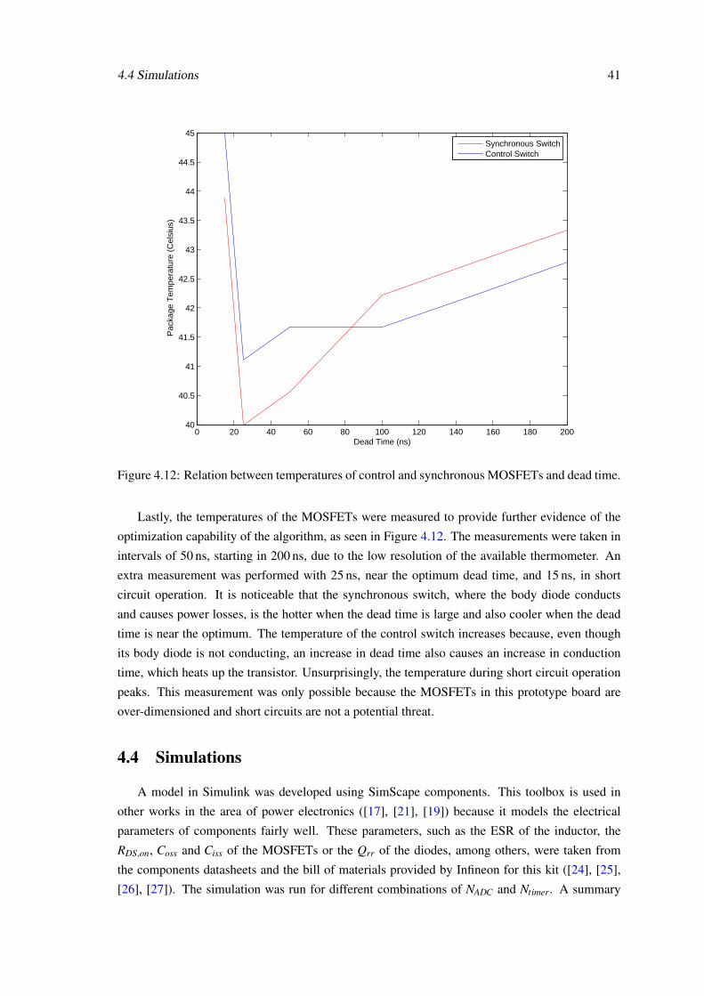
4.4 Simulations 41
0 20 40 60 80 100 120 140 160 180 20040
40.5
41
41.5
42
42.5
43
43.5
44
44.5
45
Pac
kage
Tem
pera
ture
(C
elsi
us)
Dead Time (ns)
Synchronous SwitchControl Switch
Figure 4.12: Relation between temperatures of control and synchronous MOSFETs and dead time.
Lastly, the temperatures of the MOSFETs were measured to provide further evidence of the
optimization capability of the algorithm, as seen in Figure 4.12. The measurements were taken in
intervals of 50 ns, starting in 200 ns, due to the low resolution of the available thermometer. An
extra measurement was performed with 25 ns, near the optimum dead time, and 15 ns, in short
circuit operation. It is noticeable that the synchronous switch, where the body diode conducts
and causes power losses, is the hotter when the dead time is large and also cooler when the dead
time is near the optimum. The temperature of the control switch increases because, even though
its body diode is not conducting, an increase in dead time also causes an increase in conduction
time, which heats up the transistor. Unsurprisingly, the temperature during short circuit operation
peaks. This measurement was only possible because the MOSFETs in this prototype board are
over-dimensioned and short circuits are not a potential threat.
4.4 Simulations
A model in Simulink was developed using SimScape components. This toolbox is used in
other works in the area of power electronics ([17], [21], [19]) because it models the electrical
parameters of components fairly well. These parameters, such as the ESR of the inductor, the
RDS,on, Coss and Ciss of the MOSFETs or the Qrr of the diodes, among others, were taken from
the components datasheets and the bill of materials provided by Infineon for this kit ([24], [25],
[26], [27]). The simulation was run for different combinations of NADC and Ntimer. A summary
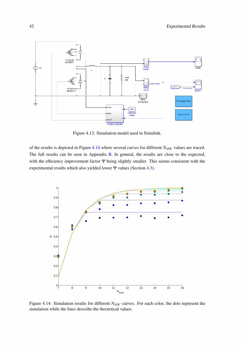
42 Experimental Results
Figure 4.13: Simulation model used in Simulink.
of the results is depicted in Figure 4.14 where several curves for different NADC values are traced.
The full results can be seen in Appendix B. In general, the results are close to the expected,
with the efficiency improvement factor Ψ being slightly smaller. This seems consistent with the
experimental results which also yielded lower Ψ values (Section 4.3).
7 8 9 10 11 12 13 14 15 160
0.1
0.2
0.3
0.4
0.5
0.6
0.7
0.8
0.9
1
Ntimer
Ψ
Figure 4.14: Simulation results for different NADC curves. For each color, the dots represent thesimulation while the lines describe the theoretical values.
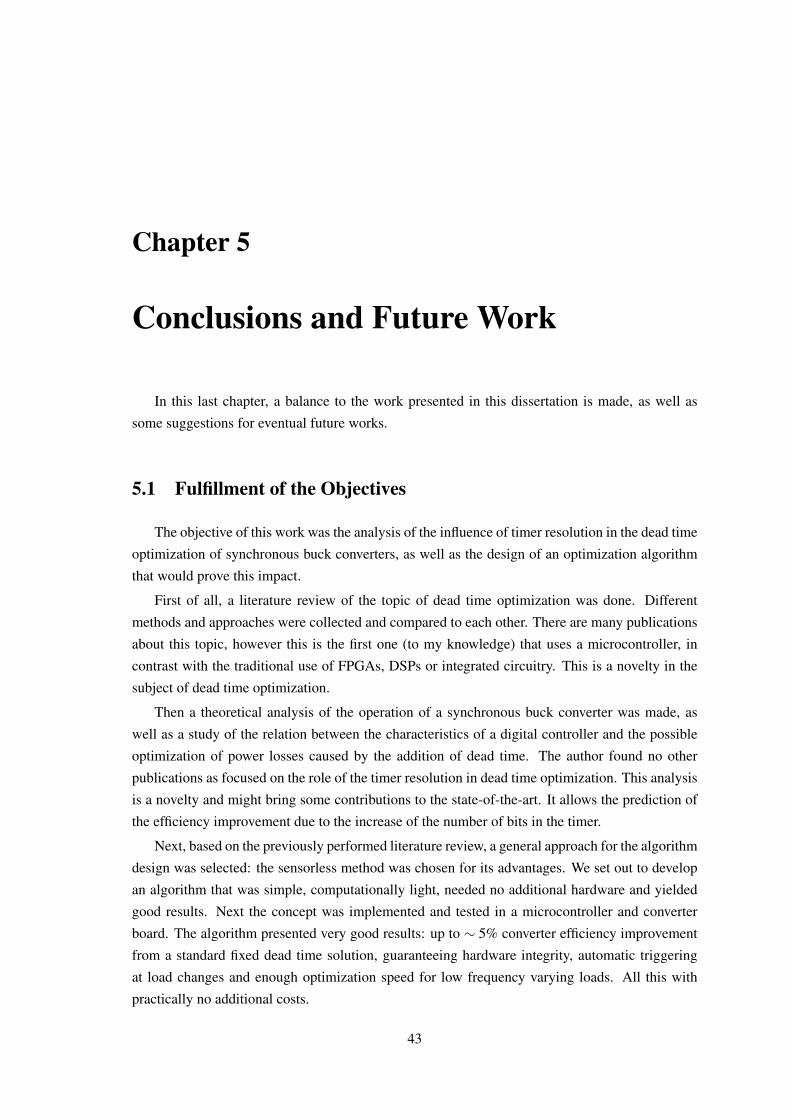
Chapter 5
Conclusions and Future Work
In this last chapter, a balance to the work presented in this dissertation is made, as well as
some suggestions for eventual future works.
5.1 Fulfillment of the Objectives
The objective of this work was the analysis of the influence of timer resolution in the dead time
optimization of synchronous buck converters, as well as the design of an optimization algorithm
that would prove this impact.
First of all, a literature review of the topic of dead time optimization was done. Different
methods and approaches were collected and compared to each other. There are many publications
about this topic, however this is the first one (to my knowledge) that uses a microcontroller, in
contrast with the traditional use of FPGAs, DSPs or integrated circuitry. This is a novelty in the
subject of dead time optimization.
Then a theoretical analysis of the operation of a synchronous buck converter was made, as
well as a study of the relation between the characteristics of a digital controller and the possible
optimization of power losses caused by the addition of dead time. The author found no other
publications as focused on the role of the timer resolution in dead time optimization. This analysis
is a novelty and might bring some contributions to the state-of-the-art. It allows the prediction of
the efficiency improvement due to the increase of the number of bits in the timer.
Next, based on the previously performed literature review, a general approach for the algorithm
design was selected: the sensorless method was chosen for its advantages. We set out to develop
an algorithm that was simple, computationally light, needed no additional hardware and yielded
good results. Next the concept was implemented and tested in a microcontroller and converter
board. The algorithm presented very good results: up to ∼ 5% converter efficiency improvement
from a standard fixed dead time solution, guaranteeing hardware integrity, automatic triggering
at load changes and enough optimization speed for low frequency varying loads. All this with
practically no additional costs.
43
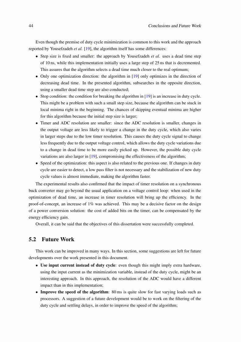
44 Conclusions and Future Work
Even though the premise of duty cycle minimization is common to this work and the approach
reported by Yousefzadeh et al. [19], the algorithm itself has some differences:
• Step size is fixed and smaller: the approach by Yousefzadeh et al. uses a dead time step
of 10 ns, while this implementation initially uses a large step of 25 ns that is decremented.
This assures that the algorithm selects a dead time much closer to the real optimum;
• Only one optimization direction: the algorithm in [19] only optimizes in the direction of
decreasing dead time. In the presented algorithm, subsearches in the opposite direction,
using a smaller dead time step are also conducted;
• Stop condition: the condition for breaking the algorithm in [19] is an increase in duty cycle.
This might be a problem with such a small step size, because the algorithm can be stuck in
local minima right in the beginning. The chances of skipping eventual minima are higher
for this algorithm because the initial step size is larger;
• Timer and ADC resolution are smaller: since the ADC resolution is smaller, changes in
the output voltage are less likely to trigger a change in the duty cycle, which also varies
in larger steps due to the low timer resolution. This causes the duty cycle signal to change
less frequently due to the output voltage control, which allows the duty cycle variations due
to a change in dead time to be more easily picked up. However, the possible duty cycle
variations are also larger in [19], compromising the effectiveness of the algorithm;
• Speed of the optimization: this aspect is also related to the previous one. If changes in duty
cycle are easier to detect, a low pass filter is not necessary and the stabilization of new duty
cycle values is almost immediate, making the algorithm faster.
The experimental results also confirmed that the impact of timer resolution on a synchronous
buck converter may go beyond the usual application on a voltage control loop: when used in the
optimization of dead time, an increase in timer resolution will bring up the efficiency. In the
proof-of-concept, an increase of 1% was achieved. This may be a decisive factor on the design
of a power conversion solution: the cost of added bits on the timer, can be compensated by the
energy efficiency gain.
Overall, it can be said that the objectives of this dissertation were successfully completed.
5.2 Future Work
This work can be improved in many ways. In this section, some suggestions are left for future
developments over the work presented in this document.
• Use input current instead of duty cycle: even though this might imply extra hardware,
using the input current as the minimization variable, instead of the duty cycle, might be an
interesting approach. In this approach, the resolution of the ADC would have a different
impact than in this implementation;
• Improve the speed of the algorithm: 80 ms is quite slow for fast varying loads such as
processors. A suggestion of a future development would be to work on the filtering of the
duty cycle and settling delays, in order to improve the speed of the algorithm;

5.2 Future Work 45
• Include second order effects on the analysis: the theoretical study of the buck converter
and the dead time optimization does not take second order effects into consideration, such
as ringing on the switching of the MOSFETs. However, these effects are present and can
affect the optimization;
• Avoid local minima: The algorithm designed in this work did not take local minima into
account. The optimization might end up "stuck" far away from the true optimum;
• Extend this work to other converter topologies: there are multiple topologies of SMPS
only in DC/DC conversion. The work presented in this paper might be adaptable to some
of these other topologies or even to other power converter types.

46 Conclusions and Future Work

Appendix A
Calculation of Real Dead Time
This appendix contains the calculation of the real dead time for a certain microcontroller-
defined dead time. The signal has to pass through the microcontroller output pins, gate driver and
MOSFET, with certain delays that are different for both rising and falling edge. The consequence
is a deviation from the defined dead time.
td,r2 td,f2ton
Ts
vgs,CS
vsw
vgs,SS
td,f1tontd,r1
P0.8
P0.4
Figure A.1: Representation of the delay between the signal out of the microcontroller pins and theswitching node voltage.
Firstly, the parameters that influence the timing of the signals must be fetched from the
datasheets of the microcontroller [4], gate driver [25] and MOSFET [24]. The parameters are
organized in table A.1.
47
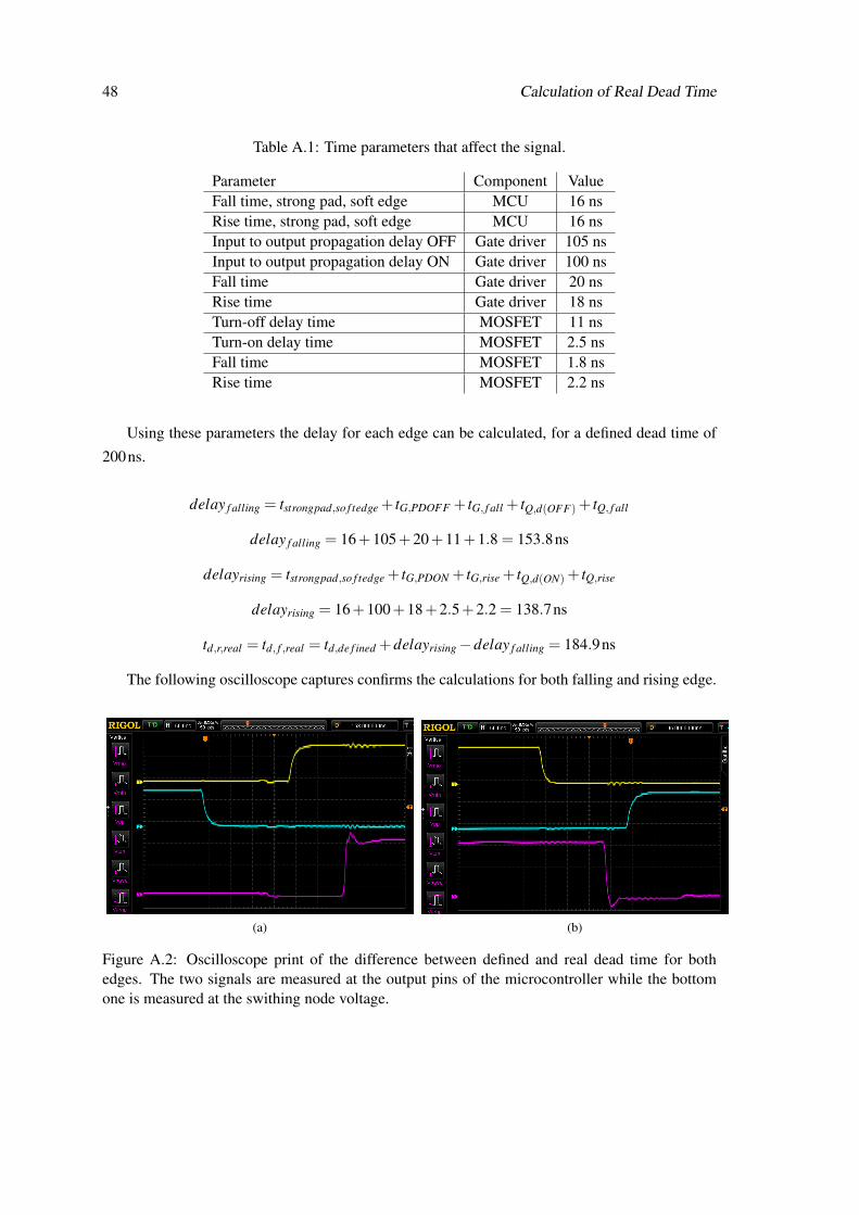
48 Calculation of Real Dead Time
Table A.1: Time parameters that affect the signal.
Parameter Component ValueFall time, strong pad, soft edge MCU 16 nsRise time, strong pad, soft edge MCU 16 nsInput to output propagation delay OFF Gate driver 105 nsInput to output propagation delay ON Gate driver 100 nsFall time Gate driver 20 nsRise time Gate driver 18 nsTurn-off delay time MOSFET 11 nsTurn-on delay time MOSFET 2.5 nsFall time MOSFET 1.8 nsRise time MOSFET 2.2 ns
Using these parameters the delay for each edge can be calculated, for a defined dead time of
200ns.
delay f alling = tstrongpad,so f tedge + tG,PDOFF + tG, f all + tQ,d(OFF)+ tQ, f all
delay f alling = 16+105+20+11+1.8 = 153.8ns
delayrising = tstrongpad,so f tedge + tG,PDON + tG,rise + tQ,d(ON)+ tQ,rise
delayrising = 16+100+18+2.5+2.2 = 138.7ns
td,r,real = td, f ,real = td,de f ined +delayrising−delay f alling = 184.9ns
The following oscilloscope captures confirms the calculations for both falling and rising edge.
(a) (b)
Figure A.2: Oscilloscope print of the difference between defined and real dead time for bothedges. The two signals are measured at the output pins of the microcontroller while the bottomone is measured at the swithing node voltage.
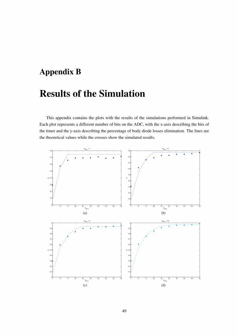
Appendix B
Results of the Simulation
This appendix contains the plots with the results of the simulations performed in Simulink.
Each plot represents a different number of bits on the ADC, with the x-axis describing the bits of
the timer and the y-axis describing the percentage of body diode losses elimination. The lines are
the theoretical values while the crosses show the simulated results.
7 8 9 10 11 12 13 14 15 160
0.1
0.2
0.3
0.4
0.5
0.6
0.7
0.8
Ntimer
Ψ
NADC = 7
(a)
7 8 9 10 11 12 13 14 15 160
0.1
0.2
0.3
0.4
0.5
0.6
0.7
0.8
0.9
Ntimer
Ψ
NADC = 8
(b)
7 8 9 10 11 12 13 14 15 160
0.1
0.2
0.3
0.4
0.5
0.6
0.7
0.8
0.9
1
Ntimer
Ψ
NADC = 9
(c)
7 8 9 10 11 12 13 14 15 160
0.1
0.2
0.3
0.4
0.5
0.6
0.7
0.8
0.9
1
Ntimer
Ψ
NADC = 10
(d)
49
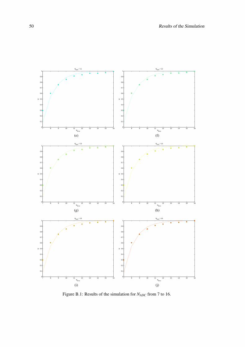
50 Results of the Simulation
7 8 9 10 11 12 13 14 15 160
0.1
0.2
0.3
0.4
0.5
0.6
0.7
0.8
0.9
1
Ntimer
Ψ
NADC = 11
(e)
7 8 9 10 11 12 13 14 15 160
0.1
0.2
0.3
0.4
0.5
0.6
0.7
0.8
0.9
1
Ntimer
Ψ
NADC = 12
(f)
7 8 9 10 11 12 13 14 15 160
0.1
0.2
0.3
0.4
0.5
0.6
0.7
0.8
0.9
1
Ntimer
Ψ
NADC = 13
(g)
7 8 9 10 11 12 13 14 15 160
0.1
0.2
0.3
0.4
0.5
0.6
0.7
0.8
0.9
1
Ntimer
Ψ
NADC = 14
(h)
7 8 9 10 11 12 13 14 15 160
0.1
0.2
0.3
0.4
0.5
0.6
0.7
0.8
0.9
1
Ntimer
Ψ
NADC = 15
(i)
7 8 9 10 11 12 13 14 15 160
0.1
0.2
0.3
0.4
0.5
0.6
0.7
0.8
0.9
1
Ntimer
Ψ
NADC = 16
(j)
Figure B.1: Results of the simulation for NADC from 7 to 16.
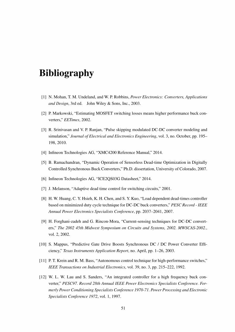
Bibliography
[1] N. Mohan, T. M. Undeland, and W. P. Robbins, Power Electronics: Converters, Applications
and Design, 3rd ed. John Wiley & Sons, Inc., 2003.
[2] P. Markowski, “Estimating MOSFET switching losses means higher performance buck con-
verters,” EETimes, 2002.
[3] R. Srinivasan and V. P. Ranjan, “Pulse skipping modulated DC-DC converter modeling and
simulation,” Journal of Electrical and Electronics Engineering, vol. 3, no. October, pp. 195–
198, 2010.
[4] Infineon Technologies AG, “XMC4200 Reference Manual,” 2014.
[5] B. Ramachandran, “Dynamic Operation of Sensorless Dead-time Optimization in Digitally
Controlled Synchronous Buck Converters,” Ph.D. dissertation, University of Colorado, 2007.
[6] Infineon Technologies AG, “ICE2QS03G Datasheet,” 2014.
[7] J. Melanson, “Adaptive dead time control for switching circuits,” 2001.
[8] H. W. Huang, C. Y. Hsieh, K. H. Chen, and S. Y. Kuo, “Load dependent dead-times controller
based on minimized duty cycle technique for DC-DC buck converters,” PESC Record - IEEE
Annual Power Electronics Specialists Conference, pp. 2037–2041, 2007.
[9] H. Forghani-zadeh and G. Rincon-Mora, “Current-sensing techniques for DC-DC convert-
ers,” The 2002 45th Midwest Symposium on Circuits and Systems, 2002. MWSCAS-2002.,
vol. 2, 2002.
[10] S. Mappus, “Predictive Gate Drive Boosts Synchronous DC / DC Power Converter Effi-
ciency,” Texas Instruments Application Report, no. April, pp. 1–26, 2003.
[11] P. T. Krein and R. M. Bass, “Autonomous control technique for high-performance switches,”
IEEE Transactions on Industrial Electronics, vol. 39, no. 3, pp. 215–222, 1992.
[12] W. L. W. Lau and S. Sanders, “An integrated controller for a high frequency buck con-
verter,” PESC97. Record 28th Annual IEEE Power Electronics Specialists Conference. For-
merly Power Conditioning Specialists Conference 1970-71. Power Processing and Electronic
Specialists Conference 1972, vol. 1, 1997.
51
52 BIBLIOGRAPHY
[13] B. Acker, C. Sullivan, and S. Sanders, “Synchronous rectification with adaptive timing con-
trol,” Proceedings of PESC ’95 - Power Electronics Specialist Conference, vol. 1, 1995.
[14] A. Zhao, A. A. Fomani, and W. T. Ng, “One-step digital dead-time correction for DC-DC
converters,” Conference Proceedings - IEEE Applied Power Electronics Conference and Ex-
position - APEC, pp. 132–137, 2010.
[15] L. Mei, D. Williams, and W. Eberle, “A Synchronous Buck Converter Using a New Predic-
tive Analog Dead-Time Control Circuit to Improve Efficiency,” Canadian Journal of Elec-
trical and Computer Engineering, vol. 36, no. 4, pp. 181–187, 2013.
[16] O. Trescases, W. T. N. W. T. Ng, and S. C. S. Chen, “Precision gate drive timing in a zero-
voltage-switching DC-DC converter,” Power Semiconductor Devices and ICs, 2004. Pro-
ceedings. ISPSD ’04. The 16th International Symposium on, 2004.
[17] J. Abu-Qahouq, H. M. H. Mao, H. Al-Atrash, and I. Batarseh, “Maximum Efficiency Point
Tracking (MEPT) Method and Digital Dead Time Control Implementation,” IEEE Transac-
tions on Power Electronics, vol. 21, no. 5, pp. 1273–1281, 2006.
[18] A. Pizzutelli, A. Carrera, M. Ghioni, and S. Saggini, “Digital dead time auto-tuning for
maximum efficiency operation of isolated DC-DC converters,” PESC Record - IEEE Annual
Power Electronics Specialists Conference, pp. 839–845, 2007.
[19] V. Yousefzadeh and D. Maksimovic, “Sensorless optimization of dead times in dc-dc con-
verters with synchronous rectifiers,” IEEE Transactions on Power Electronics, vol. 21, no. 4,
pp. 994–1002, 2006.
[20] T. Reiter, D. Polenov, H. Pröbstle, and H. G. Herzog, “PWM dead time optimization method
for automotive multiphase DC/DC-converters,” IEEE Transactions on Power Electronics,
vol. 25, no. 6, pp. 1604–1614, 2010.
[21] A. V. Peterchev and S. R. Sanders, “Digital multimode buck converter control with loss-
minimizing synchronous rectifier adaptation,” IEEE Transactions on Power Electronics,
vol. 21, no. 6, pp. 1588–1599, 2006.
[22] P. Haaf and J. Harper, “Understanding Diode Reverse Recovery and its Effect on Switching
Losses,” Fairchild Power Seminar, pp. 23–33, 2007.
[23] H. Tajiri and T. Kumano, “Input Filtering of MPPT Control by Exponential Moving Average
in Photovoltaic System,” IEEE International Conference on Power and Energy (PECon), no.
December, pp. 372–377, 2012.
[24] Infineon Technologies AG, “BSZ060NE2LS Datasheet,” 2013.
[25] ——, “1EDI60N12AF Datasheet,” 2014.

BIBLIOGRAPHY 53
[26] Bourns, “SRF1280 Datasheet,” 2011.
[27] Infineon Technologies AG, “XMC Buck Converter Kit - Bill of Materials,” 2014.


![CONVERSORES ELECTRÓNICOS DE CONVERSORES · PDF filepotência [W/cm3] IST-DEEC ... η](https://img.dokumen.tips/doc/110x75/5a7a606a7f8b9a07508d5aae/conversores-electrnicos-de-conversores-wcm3-ist-deec-80-conversores.jpg)
