Embed Size (px)
Citation preview
May 2000 Novem
THIN-FILM SOLAR CELLS
Technology Evaluation and Perspectives
R.H. Bossert *
C.J.J. Tool #
J.A.M. van Roosmalen #
C.H.M. Wentink #
M.J.M. de Vaan *
* Berenschot# Netherlands Energy Research Foundation – ECN
Netherlands, tel. +31 46 4202250, report number DV 1.1.170
This report can be ordered free of charge at Novem, PO Box 17, 6130 AA Sittard,
2
Acknowledgement/Preface
This report is the result of contract research by order of the Netherlands Agency for Energy andthe Environment (Novem, contract no. 146.150-010.1) to Berenschot and the NetherlandsEnergy Research Foundation ECN.
AbstractThe main thin-film solar cell technologies are evaluated with respect to the criteria Cost,Applicability, Sustainability and Compatibility with the Dutch PV infrastructure. Thisevaluation concerns the following technologies in particular: thin film crystalline silicon,separated into low and high temperature deposition processes (LT-f-Si, HT-f-Si), amorphoussilicon (a-(Si,Ge):H), copper indium-gallium di-selenide-sulphide (CIGS), cadmium telluride(CdTe) and dye-sensitized (DSC) solar cells technologies. For this evaluation, multicrystallinesilicon (mc-Si) is used as a reference. This means that all scores (low, high, etc.) are relative tomc-Si. Organic/polymeric cells are of special interest for the long term, but not enough data isavailable for a full analysis. Interviews with experts from industry and R&D institutions and atechnology review form the basis for this evaluation. The present status, the short- and long-term perspective are reviewed and the risk involved in the further developments is assessed, therisk being separately evaluated and weighed. To facilitate comparison the criteria are quantifiedand weighing factors are used to normalise the evaluation. Where possible, the developmentsand data reflect the expected status in 2005.
A number of interesting patterns can be observed from this evaluation. In the category Cost,a-(Si,Ge):H, LT-f-Si and DSC score better than mc-Si. In the category Applicability,a-(Si,Ge):H, and to a lesser extent CIGS and CdTe, score high. LT-f-Si scores high forSustainability, both for its low toxicity content and a high resource availability. CIGS, CdTe andHT-f-Si score low in the categorie Cost, Sustainability and Dutch infrastructure. As expected,only the a-(Si,Ge):H technology scores well on the availability of a good PV R&Dinfrastructure in The Netherlands. DSC scores relatively high on the R&D infrastructure, whereespecially the international technological position is excellent.
Industrial activities world-wide are concentrated on high-rate and low-cost manufacturingprocesses. At present industry is investing mainly in the x-Si, a-(Si,Ge):H, CIGS and CdTetechnologies. R&D is focused on improving efficiency, gaining a thorough understanding of thematerial properties and developing new deposition techniques.
The interviews with experts indicate confidence in x-Si and a-(Si,Ge):H technologies withregard to the criteria Costs, Efficiency and Risk control. The technology mapping confirmsthese expectations. A major difficulty in scaling up the CIGS and CdTe technologies is thecontrol of active layer deposition over a large area. The critical risks involved in processingLT-f-Si technologies are the deposition of the active layer and control of the material properties.The a-(Si,Ge):H and LT-f-Si are strongly related and it is expected that they can benefit fromeach other, with mutual spin-off’s and probably combined devices. HT-f-Si has a potential forhigh efficiencies, but the development time is still long and no real successful depositionprocess has been identified yet, so the level of uncertainty is high. It is anticipated that the dye-sensitised and the organic/polymeric solar cells will become important in the mid- to longerterm with advantages in Costs and Applicability. Much basic and applied research has yet to bedone on the stability for both types and the charge transport properties of organic/polymericmaterials.
During the interviews, several experts mentioned that more co-operation between researchgroups and the industry is important on a European and intercontinental level.
Keywords: thin-film solar cells, technological evaluation, perspectivesContains: 24 tables, 7 figures and 99 references
3
CONTENTS
1. INTRODUCTION 5
2. EVALUATED TECHNOLOGIES 62.1 Crystalline silicon 62.2 Amorphous silicon a-(Si,Ge):H 62.3 Thin-film crystalline silicon 72.4 Cu(In,Ga)(Se,S)2 72.5 CdTe 72.6 Dye solar cells and organic solar cells 72.7 Others 8
3. CRITERIA AND WEIGHING-FACTORS 93.1 Cost 93.2 Applicability 93.3 Sustainability 103.4 PV R&D in The Netherlands 113.5 Summary 11
4. INTERVIEWS WITH KEY FIGURES 124.1 Research approach 124.2 Significant patterns from the expert scores 134.3 Overview of the expert interviews 134.4 International aspects 19
5. TECHNOLOGY MAPPING 215.1 Method and limitation 215.2 Technology maps 225.3 Summary 31
6. LITERATURE REVIEW FOR COST AND SUSTAINABILITY 326.1 Module production costs 326.2 Energy payback time 336.3 Availability of resources 356.4 Toxicity 37
7. DISCUSSION 397.1 Evaluation matrix 397.2 Relevant market parties 41
8. CONCLUSION 43
9. REFERENCES 44
APPENDIX A: QUESTIONNAIRE FOR THE INTERVIEWS 50
APPENDIX B: INDIVIDUALS INTERVIEWED 53
APPENDIX C: EXPERT SCORE 55
APPENDIX D: THE HELIANTHOS PROJECT 58

4
5
1. INTRODUCTION
Thin-film solar cells will become an important resource for our sustainable energy supply in thenear future. At present, several PV technologies are available with different properties in termsof efficiency, maturity, stability and applicability. Novem B.V., the Netherlands Agency forEnergy and the Environment, is planning to conduct a technology review to support the processleading to a new four-years programme. Several thin-film solar-cell research activities are beingsupported by Novem as a part of the National R&D Programme on Photovoltaic Solar Energy(NOZ-PV). In this context, several thin-film solar-cell technologies have to be evaluated withregard to their prospects and feasibility. The seven evaluated technologies are multicrystallinesilicon, amorphous silicon, thin-film silicon, Cu(In,Ga)(Se,S)2, CdTe, dye-sensitised solar cellsand polymer solar cells. This study has been conducted by Berenschot B.V., together with theNetherlands Energy Research Foundation ECN. The results of this report will be used as aguideline to determine the most promising thin-film solar-cell technologies with potential forDutch research and industrial activities.
The basis for the evaluation is an assumption about the status of the technologies in 2005.Throughout the report, this is the reference date, unless otherwise specified. The timeframe of2005 corresponds most closely to the various developments that are currently under way, costsprojections, market introduction, R&D programmes, etc. Of course, for some technologies anddevelopments this will be somewhat earlier or later. Specifically for HT-f-Si and polymericsolar cells, but also to some extent for LT-f-Si and dye-sensitized solar cells, the perspective insome parts of the report is more to the mid- to long term. The technologies have beeninvestigated with regard to their future potential and the risks involved, in order to design astrategic compass for thin-film solar-cell activities. This report starts with a short description ofthe seven technologies investigated. The reasons for selecting these specific thin-filmtechnologies are also given. Criteria and weighing factors have been developed in order toconstruct a transparent quantitative method of evaluating the different technologicalpossibilities. The criteria are clustered within the dimensions of Cost, Applicability,Sustainability and Compatibility with the Dutch PV R&D infrastructure. Weighing factors areused to balance the importance of the various criteria.
The help and involvement of several thin-film PV experts have broadened the context of thissurvey. We are grateful to key figures who were interviewed for sharing their vision andopinions on the various technology developments in an open and constructive way. Theopinions given in these interviews are summarised in Section 4.
To develop a better understanding of and detailed insight into the technologies, theircharacteristics and risks, we constructed several technology maps to identify critical technologysteps within each thin-film production process. These steps are given scores on a wide scalefrom the laboratory stage to the industrial production phase. The results have been clusteredwith the interview results and used to make an overall matrix with criteria analyses. Especiallyin the analysis and evaluation of the risks involved the uncertainty in the time horizon and thedifferent perspectives are expressed. Finally the technology evaluation is discussed andcomments are made about the results.
6
2. EVALUATED TECHNOLOGIES
The selection of technologies to be evaluated was based on the thin-film technologiesinvestigated within the current NOZ-PV programme: amorphous silicon (a-(Si,Ge):H), thin-filmcrystalline Si, DSC (dye-sensitised solar cell), and organic/polymeric bulk heterojunctionstogether with some additional technologies that are close to market introduction if not on themarket already: Cu(In,Ga)(Se,S)2 and CdTe. Crystalline silicon is the dominant PV-material onthe market and all thin-film technologies will have to compete with it to generate a certainmarket share. Multicrystalline silicon is therefore used as a reference and used to scale the dataof the evaluation table.
2.1 Crystalline silicon
The thin-film technologies will continue to have to compete with crystalline silicon (x-Si) in thefuture as they do now. The present total market share of crystalline silicon is 85%. For thatreason, crystalline silicon technology is used as a reference case for the thin-film technologies.Instead of using the current state of x-Si, we have made an estimation of the status of the mc-Sitechnology in 2005. This method is used to compare the various thin-film technologies.
It is expected that, by 2005, feedstock material will consist of custom made solar-grade silicon(SOG) and electronic-grade scrap at a ratio of 50-50%. While mc-Si will still be a wafertechnology, part of the wafers will be produced by direct casting (e.g. EFG, RGS, string ribbon)instead of by directional solidification and sawing. The processing of the wafers into cells willstill be mainly based on the well-known techniques:
• wet etching for saw damage / surface removal and texturing• spraying, spinning, screen printing or similar techniques to apply a P-source
followed by diffusion for pn junction formation• (PE-)CVD SiNx anti reflection coating• screen printing and sintering of metallisation• soldering or ultrasonic welding to interconnect strings• laminating the cells using EVA/glass/tedlar, with fully plastic encapsulation as an
alternative
To ease the interconnection, alternative device layouts (e.g. Pin Up Module, Bultman 2000) areexpected for part of the modules. It is expected that the efficiency of the wafers resulting fromdirect solidification will be around 16%, while the efficiency of the sheet and ribbon materialwill be around 13.5% (module efficiencies). About 25% of the NOZ-PV solar-cell R&Dfunding was attributed to crystalline silicon in 1999.
2.2 Amorphous silicon a-(Si,Ge):H
Amorphous silicon, a-(Si,Ge):H, is the only thin-film technology that already has a substantialmarket share (15%, Maycock 1999), and it is generally believed to be the first thin-filmtechnology that can compete with x-Si. The discussion on a-(Si,Ge):H will be based on threepossible production methods: batch deposition on a glass superstrate, roll-to-roll deposition on aflexible substrate (e.g. steel as done by United Solar; see Yang, 1998; Nath, 1998; Guha, 1997),and roll-to-roll on a temporary superstrate (Helianthos by AKZO-Nobel; see Middelman, 1998;Schropp, 1998). For the evaluation table, the triple junction on a flexible substrate will be usedmainly. About 40% of the NOZ-PV solar-cell R&D funding was attributed to a-(Si,Ge):H in1999.
7
2.3 Thin-film crystalline silicon
Thin-film crystalline silicon (f-Si) covers a broad technological field, which is usually dividedin two main routes:• High-temperature replacement of thick, expensive, silicon by a thin (< 50 µm) silicon film
on a low-cost substrate• Low-temperature the use of micro crystalline silicon < 5 µm in an amorphous silicon-like
or amorphous silicon-based structure.
A lot of research has been done on the high-temperature approach, as it has the potential toresult in large-grain material with an efficiency close to that of multicrystalline silicon. Thesilicon film on substrate can be processed into cells with conventional mc-Si technology. Theonly film silicon produced on a pilot scale is operated by AstroPower.
The low-temperature route results in a microcrystalline silicon film. The technology closelyresembles that of amorphous silicon. Tandems are often made with both micro crystalline andamorphous silicon. In particular, the results of the Japanese company Kaneka (>10%) received alot of attention.
In addition, a number of intermediate routes are being developed, based on the growth of large-grain material at low temperatures using plasma-assisted, ion-assisted, or liquid-assisted growth.Clearly there are many options for making thin-film silicon, although no favoured approach hasbeen chosen yet. With the reliability and efficiency character of x-Si compared with the natureof f-Si, it is believed that specific thin film developments have a high potential. This could bethe reason for the amount of attention given on this technology world-wide. About 15% of theNOZ-PV solar-cell R&D funding was attributed to f-Si in 1999.
2.4 Cu(In,Ga)(Se,S)2
Although Cu(In,Ga)(Se,S)2 is not being investigated in the current NOZ-PV programme, it is animportant material to incorporate in this evaluation. Many R&D and industry groups world-wide are investigating it. Besides, commercial Cu(In,Ga)(Se,S)2 modules have entered themarket (Siemens Solar shipped 300 kWp in 1999, Maycock, 2000) with top efficiencies of over11% (Eikelboom, 1999; Karg, 2000). Moreover, with respect to the other technologies currentlybeing developed, Cu(In,Ga)(Se,S)2 represents an entirely different set of material properties andprocessing techniques.
2.5 CdTe
Like Cu(In,Ga)(Se,S)2, CdTe is also not included in the current NOZ-PV programme. In 1999CdTe was mainly produced for consumer electronics (by Matsushita; with a production ofaround 1.5 MWp, it constituted less than 1% of the total shipped PV volume, Maycock 1999).Several industries (e.g. BP Solarex, Antec, First Solar; Maycock 1999) have plans to start largerscale CdTe production for outdoor applications. It is widely accepted that CdTe is a promisingthin-film technology. Special attention will be given to the possible toxicity of CdTe withrespect to the use of Cd, especially in relation to Dutch legislation.
2.6 Dye solar cells and organic solar cells
Actually, organic solar cells are a set of several different technologies, ranging from the well-known dye-sensitised solar cells (DSC, dye cell) via the antenna cell, and molecular organicsolar cells to bulk heterojunction solar cells and completely polymeric devices. Because it isbelieved that the dye cell is closest to market introduction, this type will be evaluated separately.The other possible organic solar cell concepts will be evaluated in less detail. About 20% of theNOZ-PV solar cell R&D funding was attributed to organic solar cells in 1999.
8
2.7 Others
Several other materials and technologies have not been incorporated in this evaluation. That byno means implies that the authors believe that those technologies are not of interest or have nopotential. It simply means that those technologies are beyond the scope of the presentevaluation.Materials such as InGaP and AlGaAs may well be very interesting as possible future high-efficiency technologies. The main issue for III/V solar cells is the cost of the substrate. Recentlyvery promising results were obtained with a lift-off process that allow re-use of the substrate(Bauhuis, 2000). This process is claimed to be competitive in 10 years with other low-costthin-film options. At this moment, the main application for this type of solar cells is inconcentrator systems. Concentrator systems are, however, not included, because concentratorsystems are less relevant to the Dutch situation with its high diffuse part of the total irradiation.Mechanically stacked tandem structures such as InGaP on x-Si or a-Si on x-Si, are also notincluded. The same holds for system approaches that either decrease the generation costs of PVor increase the overall efficiency of PV systems, such as thermal electrical hybrid systems(sometimes referred to as PV-Combi or “zonne-WKK”).
Although research on very-high-efficiency PV technologies is necessary for the long termdevelopment of PV (Sinke, 2000; Green, 2000; Kazmerski, 2000a), such materials are notincluded here because this would involve true basic research on (yet unknown or unexplored)materials and device structures. Conventional multi-junction devices, which might also yieldhigh efficiencies, may be reasonably served by research on the individual materials andtechnologies in the tandem structure.
9
3. CRITERIA AND WEIGHING-FACTORS
In order to evaluate the thin-film technologies, various criteria and weighing-factors have beenidentified. To make the evaluation more flexible, the criteria have been grouped into fourcategories. Within each category the weighing-factors are scaled so that the sum of the factors is1 within each category. This means that weighing-factors within different categories can notsimply be compared. To do the actual comparison, each category is given an additional weight.Although this might seem to complicate the analysis, it has the advantage that the reader him- orherself can easily change the importance of the different categories. For example, possibleweighing-factors for different market players are given at the end of Section 7.The four categories in which the various criteria have been combined are the three factors asevolved from earlier evaluation work (Roosmalen, 1995): Costs, Applicability andSustainability, completed with the Dutch PV R&D infrastructure.
3.1 Cost
Within the category Cost, three criteria are evaluated:
• module production costs (€ / Wp )The BOS costs are omitted because they largely depend on the type of system inwhich the module will be used (e.g. grid-connected vs stand-alone).
• efficiencyEven within the same system category, the BOS costs can vary considerably fromone technology to another (e.g. due to differences in module area in order to obtaincomparable output). This effect is partly overcome by using the module efficiencyas a criterion.
• riskThis criterion indicates the maturity of the technology. It is measured by means oftechnology mapping, and also includes the amount of time expected before thistechnology will live up to the promises it makes.
Because the production costs are generally mentioned as the greatest obstacle to the large-scaleintroduction of PV (Kampen, 1999; Groenendaal, 2000), this criterion has been given a weightof 0.5. Because the importance of efficiency is partly incorporated in the €/Wp criterion, theweight for the criterion “efficiency” has been set at 0.2, while the weight for “risk” has been setat 0.3
Other possible cost criteria such as module costs/kWh, module costs/m2, economic lifetime, andthroughput in production, have been omitted in this evaluation. Most of those criteria are eitherrelated to the criteria that are being evaluated, or depend more on the specific application(location) than on the technology (e.g. costs/kWh)
3.2 Applicability
Within the category Applicability, three criteria are evaluated:
• design, colourIn some cases, design may be the decisive factor for PV application. At present,design and colour is the added value of PV and sometimes more important than thebasic economy of electricity generation.
10
• product diversityThis criterion measures the flexibility of a possible production facility in order tosee if it is possible to serve different markets with a single production line. In otherwords, it indicates which market segments can be served without needing separateproduction lines for each market.
• market shareThis criterion is partly correlated to the previous one, as it measures the potentialmarket for a technology.
Because product diversity and market share are partly correlated with each other, and design +colour are (at least at the moment) important items, the weight of design + colour is set at 0.4.Market share and product diversity have a comparable importance, and have therefore beengiven the same weight (0.3).
Other criteria such as technical lifetime, reliability, flexibility (here used as pliable),standardisation, and maintenance, are not included because their importance is mainly on asystems level (e.g. maintenance), because they do not discriminate between the thin-filmtechnologies (e.g. standardisation), or because they are included in other criteria.
3.3 Sustainability
Also within the category Sustainability three criteria are identified:
• energy payback timeThe energy payback time is an often used indicator for the sustainability of solarcells. The technical lifetime of solar modules dominantly determined by theencapsulation protecting the solar module from environmental attack.. It is assumedhere that, in 2005, the quality of the encapsulation method used will be such that alltechnologies will have a comparably long lifetime, which well exceeds the energypay-back period.
• availability of resourcesIf only a limited volume of the solar cells can be produced due to limited resourcesof crucial materials, the technology cannot be a long-term option.
• toxicityAn important point in sustainability is the ecological footprint of a technology. Toestimate this, a life-cycle analysis (LCA) of all technologies would be necessary.That goes beyond the scope of this survey. Moreover, it is impossible to make a fullLCA for germinating technologies. To quantify the toxicity of the thin-filmmodules, a different approach has been used. Instead of performing the completeLCA, the effect of an accident (burning of the module) on people near the accidenthas been estimated.We have chosen to evaluate the toxicity by emissions to air because:
• according to Steinberger (1998) emissions to water from a broken panel ona roof are insignificant;
• there is only a small amount of leaching of metals into the soil due to abroken panel (Steinberger, 1998);
• most toxicological data for materials are known on emissions to air(Heijungs, 1992).
Other sustainable criteria, such as recycleability, health aspects, and safety, have not beenincluded because they either go beyond the scope of this investigation (health aspects), can onlybe evaluated if detailed module design and materials are known (recycleability), or are includedin other criteria (safety in production as part of the costs).

11
3.4 PV R&D in The Netherlands
This survey has been undertaken in order to guide the Dutch NOZ-PV programme. The DutchPV R&D is therefore considered as a separate category within this evaluation. Within thiscategory a distinction is made between industrial and institutional (e.g. universities, researchinstitutes) R&D activities. Those criteria are given the same weight.
The Dutch infrastructure in related or supporting technology fields, such as the expertise ofPhilips on polymeric LED’s is not included in the evaluation. Due to this limitation, the Dutchinfrastructure is probably underestimated for those technologies on which only limited PV-related research has been conducted. Fundamental knowledge of those materials (e.g.Cu(In,Ga)(Se,S)2 and CdTe) is lacking, but knowledge on the individual production steps iscertainly available, either from the other solar-cell technologies, or in related industrial areas.
3.5 Summary
The table below provides a brief summary of the selected criteria and their respective weight.This list is definitely not conclusive for evaluating the potential of PV. In this evaluation, ofvarious thin-film solar cell technologies are compared with each other in terms of theirpotential. Therefore, criteria that are important for the introduction of (thin-film) PV in general,but that do not discriminate between the various thin-film technologies (e.g. a distribution andsales network) are not included. Also, some criteria are beyond the scope of this survey (e.g. acomplete LCA).
Overview of weighing factorsCriterion Weight CommentsCost
cost/Wp 0.5 €/Wp module production costsefficiency 0.2 on a module level
risk 0.3 maturity of the technology
Applicabilitydesign, colour 0.4 possibilities for choosing properties, outlook
product diversity 0.3 using a single production facilitymarket share 0.3 possible market share
Sustainabilityenergy payback time 0.4
available resources 0.4 which quantity (Wp) that can be produced using the assumedproduction technology
toxicity 0.2 based on emission in a fire
PV R&D in NLindustrial 0.5 number of people active in PV-R&D in industry
others 0.5 number of people active in PV-R&D in universities,research institutes
12
4. INTERVIEWS WITH KEY FIGURES
4.1 Research approach
In this investigation we opted for a broad expert orientation on the various thin-film solartechnologies. We have spoken with different Dutch and foreign experts and asked them to scorethe technologies using the various criteria of the evaluation. The experts were selected in such away that all technologies would be covered. During the personal interviews, these experts weregiven the opportunity to describe their vision, expectations, research experiences, risks andresults. The interviews were conducted by an impartial party, Berenschot, with the objective ofdrafting an overview with qualitative judgements for each thin-film solar-cell technology route.The experts were given the chance to elucidate the scores they gave for each technology.Research data and publications were presented during some interviews. The questionnairecontained in Appendix A served as a guide for the interviews. A detailed list of the expertsinterviewed is provided in Appendix B.
The interview results were supplemented with information from discussions held during thefollowing conferences:- Photovoltaic Devices, Thin-film Technology, organised by European Research Conferences
(EU) in Berlin, 31 March - 4 April 2000- National Center for Photovoltaics Program Review Meeting (NREL) in Denver, 12-16 April
2000- 16th European Photovoltaic Solar Energy Conference (EU) in Glasgow, 1-5 May 2000
The experts consulted within the framework of this investigation are:
general thin-film technologies- T. Bruton, BP Solarex (UK) 1
- S. Kato, New Energy and Industrial Technology Development Organization (NEDO),Japan 2
- P.W. Kwant, Shell International B.V.- J. Wilkie, Shell Solar B.V. and R.J.C. van Zolingen, Shell Solar Energy BV- P.D. Maycock, Photo Voltaic Energy Systems Inc. (USA)- B. von Roedern, National Renewable Energy Laboratory, NREL (USA)- W.C. Sinke, J.A.M. van Roosmalen, H.H.C. de Moor, ECN Solar Energy3
- G. Willeke, Fraunhofer Institut für Solare Energiesysteme (D)
x-Si- B. Wiersma, Sunergy- G.P. Wyers, A. Schönecker, ECN Solar Energy3
a-(Si,Ge):H- G.J. Jongerden, Akzo Nobel- M.C.M. van de Sanden, Eindhoven University of Technology- R.E.I. Schropp, Utrecht University
1 No matrix data available, only private communication2 Only matrix data available, no private communication3 Resulted in one matrix response of ECN
13
f-Si- A. Goossens, Delft University of Technology- M. Zeman, Delft University of Technology
Cu(In,Ga)(Se,S)2
- M. Powalla, ZSW Materials Science (D)- P. van der Vleuten, Free Energy Europe B.V.
CdTe- D. Bonnet, Antec Solar GmbH (D)
Organic Solar cells- J.W. Hofstraat, Philips Electronics Nederland B.V.- J.C. Hummelen, University of Groningen- H. Zuilhof, Wageningen University- J.A.M. van Roosmalen, ECN Solar Energy3
4.2 Significant patterns from the expert scores
In Appendix C an overview is given of the scores of the experts on the various criteria for theinvestigated technologies. Some interesting patterns can be observed from these tables.
CostWith the possible exception of f-Si, the thin-film technologies all score better than mc-Si on themodule costs/Wp. The scores on the efficiencies of the thin-films show more variation. f-Si,Cu(In,Ga)(Se,S)2 and CdTe score the best (although still lower than mc-Si). The organic solarcells (both DSC and full organic) have the lowest score. On the risk criterion, both organic celltechnologies score the highest, and a-(Si,Ge):H the lowest. The scattered score of f-Si can be anindication of the different perspectives of the respondents (HT-f-Si vs LT-f-Si). It is obviousthat the risk for all thin-film technologies is higher than for mc-Si.
SustainabilityAll thin-film technologies score better than mc-Si on the energy payback time, with a-(Si,Ge):Hhaving the highest score. Again, the scores on f-Si are scattered. The score on the toxicity of themodule materials is high for Cu(In,Ga)(Se,S)2 and CdTe, modest for both organic solar cells,and low for the silicon devices. A comparable score is given on the availability of raw materials.
ApplicabilityThe table indicates that all thin-film technologies have comparable scores on all criteria in theapplicability category. The product diversity of mc-Si is believed to be less flexible compared tothat of the thin-film technologies.
Dutch PV infrastructureThe Dutch PV R&D infrastructure for mc-Si, a-(Si,Ge):H, f-Si, DSC and the full organic cells isestimated to be highly developed by the experts. The R&D structure for Cu(In,Ga)(Se,S)2 andCdTe is seen as being poorly developed.
4.3 Overview of the expert interviews
Besides the score on the various criteria, also discussion with the experts revealed noteworthyinformation. This information is summarised below, together with results from the visits to thevarious PV conferences. The results are summarised per technology.
Crystalline silicon (x-Si)Crystalline Si (x-Si) technology has benefited from the fast-paced research in the semiconductorindustry and is currently the dominant PV technology. Experts believe that further development

14
could still lead to a significant further reduction in production costs. The results of theinterviews show a strong belief in the good performance of x-Si in terms of the criteria:efficiency, technology control, toxicity, the availability of raw materials, market share and theDutch PV infrastructure. The perception of the issues cost/Wp, design and product diversityshows a reasonable and neutral score. The x-Si technology is by far the most developedtechnology and shows in the response few 'no comment' signs.
The interviews revealed some interesting information, a short overview of which is given on thebasic topics. The developmental activities focus on:
− decreasing the cost of the silicon− increasing the module efficiency− automation of the production and increasing the throughput.
As silicon is the most important cost factor a lot of effort is put into:− new routes to produce solar grade silicon feedstock at reduced cost to secure its
supply− direct crystallisation of silicon into sheets or ribbons, avoiding significant kerf
losses− the use of thinner wafers.
In the processing of the silicon wafers into solar cells and in the manufacturing of the modulesthe following issues are considered important:
- the ability to process wafers made of solar-grade feedstock- understanding the processes of passivation and gettering in relation to defects and
impurities present in the silicon to improve the material quality- the increase of cell efficiency up to 16% and higher- the processing of thinner wafers and sheets down to 100 µm or below
- the need for light trapping and surface passivation- development of metallisation and interconnection techniques, able to handle fragile
and uneven cells- the reduction of the encapsulation costs.
Last but not least, automation and increase of the plant size from the now typical 10 MWp perannum to 50 MWp and beyond, will have a significant impact on the module cost.The focus is on:
- integrating the processes, e.g. sealing and framing- avoiding batch-type production processes, such as soldering, or wet chemical cleaning- improving the process control.
It is believed that the x-Si technology will maintain a major market position for at least another10 years. This will be allowed by:
- a reduction of the production costs by 40-70% for PV systems that is expected withinseveral years
- the improvement of the market applicability (e.g. the compatibility with the buildingsector).
Thin-film silicon (f-Si)Thin-film silicon is usually divided up according to the silicon deposition conditions in high andlow-temperature f-Si (respectively HT-f-Si and LT-f-Si for short). The experts most involved inresearch on film silicon indicate that though this subdivision clearly proved its value during thelast 10 years, there is a trend of combining aspects of both routes.
It can not be deduced from the survey itself whether film silicon was meant to be the high- orlow-temperature approach. A much clearer picture could be drawn in the interviews.
15
High-temperature film silicon (HT-f-Si)The evaluation by the experts indicates serious doubts concerning the criteria: Modulecosts/Wp, Efficiency, Energy payback time and Technological risks. Though they did notexplicitly mention it, the respondents probably thought of the growth of silicon by CVD or LPEon ceramics or low-cost silicon when filling in the questionnaire.
The advantage of the HT approach is the high efficiency that can be obtained. High depositiontemperatures can result in a good crystallographic quality of the silicon absorber. Also, theprocessing of the silicon film can be compatible with standard crystalline silicon technology.The promises have not been fulfilled, however. Growth on a non-crystalline silicon substratehas not yet resulted in a good crystal structure of the film.Clearly, a break-through is needed. If a high-quality film can be deposited on a low-costsubstrate, other research topics are:
- throughput of the film deposition- light engineering- surface passivation- maintaining a good material quality during the processing
The potential of HT-f-Si has to be judged against the possible availability of low-cost siliconand the direct growth of silicon sheets. Right now, it can be considered a high-potential, high-risk option.
A recent development is the re-use of the expensive mono-crystalline substrate using a lift-offprocess (Feldrapp 2000, Bilyalov 2000, Catchpole 1998; Rinke, 2000). This could result inefficiencies approaching that of thin mono-crystalline silicon wafers.
Low-temperature film silicon (LT-f-Si)Those experts who mentioned LT-f-Si, are positive. This is certainly influenced by the goodresults of the Kaneka company (Japan), which obtained efficiencies of over 10% for microcrystalline silicon on a glass substrate.
Amorphous silicon research and the LT-f-Si route can be considered as one technology field.Especially if the expertise on amorphous and crystalline silicon is combined, a strong positioncould be obtained. The main issues that should be given attention are:
- the crystal structure of the films and the electrical activity of the grain boundaries- optical and electrical modelling of the device structure- enhancement of the growth rate
Right now the Dutch PV R&D infrastructure is relatively weak compared to the internationalresearch activities, which are really booming. There is a lot of expertise on the silicondeposition and cell processing, but little on the material properties and the designconsiderations. Some experts expect that film silicon whether low-temperature or high-temperature or a combination of the best of the two will become the dominant technology on thelong term (2020), replacing crystalline silicon.
Amorphous Si (a-Si)The a-Si technology has scored well on the criteria: cost/Wp, energy payback time, non-toxicity,availability of raw materials, infra structure, expected market share and product diversity. Thereare some doubts on the properties: efficiency and technological risks.
The tendency in a-Si research and production is to go to multi-junction devices to increaseefficiency and stability. United Solar reached a 10% stabilised record module efficiency(30 x 30 cm2). Nevertheless, some groups claim that single junction cells have the bestprice/performance ratio; 8% large-area (910×455 mm2) module efficiencies have been obtained
16
(Tawada, 1999). Amorphous silicon is the second best of the technologies rated within theoverall matrix, with room for further improvement.
The main R&D issues that could be identified from the interviews and conference visits are:- better understanding of the material structure of the films- better modelling tools to optimise the device structure- new approaches to improve the deposition processes
In order to obtain high stabilised module efficiencies, a thorough understanding of the materialsand processes is needed. Research in this area is directed towards:
- the material structure of the films on atomic and nano scales- the nature and control of defects in pure and alloyed materials in particular:
- the behaviour and role of H- doping and carrier mobility
A field becoming increasingly important when using tandem structures is device physics:- optimisation of the thickness and doping profiles of the different layers to maximise the
current and minimise the light-induced degradation (Stäbler-Wronski effect)- light management / light trapping by modelling scattering and reflections at front and
back contacts
A better understanding of the physics and chemistry of the deposition processes is needed:- to control the structure of the layer- to enhance the deposition rate while maintaining a good (enough) material quality
- to be able to apply successfully new deposition techniques like:- hot-wire chemical vapour deposition (University of Utrecht)- cascade arc deposition (Technical University of Eindhoven)- to be able to use new substrate materials, such as a temporary superstrate for later
transfer to polymer foils (Middelman, 1998)
Novel device production technologies are being explored to obtain a higher throughput,efficiency and yield and lower costs (several studies are being conducted within the EU (e.g.Korevaar, 2000), Japan and the USA). The industrial perspective of scaling up the productionvolume of a-Si appears to be promising, taken into account the amount of investments made byseveral industries. Automation of deposition and assembly is being researched by United SolarSystems Corporation, which is designing the process for a 25 MWp plant.The main industrial players in this field are United Solar, Solarex and Kaneka. Akzo Nobel (TheNetherlands) is developing an new production method using a temporary superstrate(Helianthos project). Fuji is developing the new SCAF-concept (Ichikawa, 1999) The Dutch PVinfrastructure (know-how and industry) appears to be competitive with the global developmentson a-Si technology.
Cu(In,Ga)(Se,S)2 (CIGS)The interviews indicate that the costs/Wp is promising and the efficiency is the highest amongthe thin films. It is believed that CIGS together with CdTe will conquer their market share onprice and the use of relatively simple production technologies. The homogeneously blackappearance of the present Siemens CIGS modules may represent an important advantage withrespect to the aesthetics. However there is a feeling that the risks involved are considerable andthe availability of raw material is an important issue as well. The Dutch PV infrastructure ispoorly developed.Though many question marks (and lack of expertise) on several criteria are given in thequestionaire, the response is in good agreement with the general opinion that can be heardduring the conferences and workshops.
17
The basic understanding of the material, properties and processing has increased significantlyover the past few years. However, an issue that has remained a concern is the complex nature ofthe phase diagram, that makes it difficult to obtain a reliable and robust large-area deposition.The main R&D issues that could be identified in the interviews were in the field of:
- device physics and materials science to understand:- the structure of the heterojunction and the interfaces in relation to:
- development of new cadmium free window layers- the nature of the contacts, the effect of buffer layers in order to prevent
degradation- point defects and the effect on the electrical properties of the device- development of wide band gap materials, such as CuInS2 (Klenk, 2000)
- process development- to improve the yield of the present vacuum deposition of the metals and
selenisation- to develop new low-cost non-vacuum processing- CIGS on flexible substrates (Rudmann, 2000; Jacobs, 1998; Kessler, 2000)
When assessing the potential of CIGS it should be realised that many routes exist and especiallywill be available to manufacture CIGS and that a wide range of compositions is possible for thisfamily of compound semiconductors (Eberspacher, 2000; Güldner, 2000; Klenk, 2000; Schock,2000).
CIGS is at the point of the first pilot-production. Siemens Solar has a running pilot line andshipped 300 kWp in 1999. Though the module efficiency is very good with more than 11%, amajor concern is the yield (Karg, 2000). Würth Solar has made impressive progress and isplanning pilot-production to start mid-2000 on 60 x 120 cm2 modules (Powalla, 2000; Powalla,2000a). EPV is offering production lines (EPV, 2000), although the first still have to be realised.
CdTeThe general expectation is that CdTe will have a good balance of cost/Wp and efficiency. It is amaterial very easy to make with an almost ideal bandgap. It obtained a good score onapplicability. However, the cadmium issue could influence the market perspective. The scorefor risk is indeed higher than to be expected from the relative maturity of the technology. In theinterviews the toxicity and availability of raw materials is considered a drawback for CdTe. TheDutch PV infrastructure is poorly developed.
In many respects CdTe resembles CIGS. It can be produced with similar techniques, thoughmuch easier. It does not have the difficulty of a complex phase diagram, but it has not thepossibility to tune the composition either. The issues that need to be addressed are:
- device physics and materials science- point defects (deep-level impurities) and the influence on the electrical
characteristics.- the nature of the CdS/CdTe heterojunction- grain boundary passivation and the interdiffusion across the junction and grain
boundaries (Durose, 2000; Özsan, 2000; Romeo, 2000)- manufacturing technology
- uniformity on large-areas- novel deposition techniques that require lower temperature processing- high speed deposition- processes that generate less waste material- improved contact technologies that show good long-term stability.
CdTe is at the point of first production. Matsushita is already in production (1.5 MWp),however for consumer electronic applications. BP Solarex has started pilot-production inCalifornia using an electrochemical deposition process. This is despite the very strict
18
regulations, indicating that an environmental problem during production can be prevented.Being able to deposit homogeneously on 60 cm x 155 cm2 TCO glass substrates efficienciesover 9% could be obtained (Özsan, 2000).First Solar is scaling up to 100 employees with itsnew thin-film CdTe inline factory (20 MWp). Antec Solar GmbH is planning to start its firstCdTe production line this summer (Antec, 2000).
The dye cell and organic solar cellsOrganic materials are generally considered to offer a range of new possibilities in terms ofmaterials use (materials design) and device concepts. Although it is found to be still difficult tomake firm statements on the different technologies in this category, there is a reasonable tostrong belief that they may be produced at (very) low cost. Uncertainty exist on the efficiencylevels that may be expected on the medium- to long term. So far, they are generally notcategorised as true high-efficiency approaches, but it is acknowledged that the full potential maynot be seen yet.Basic issues and questions are mainly related to:
- intrinsic and device stability (and hence, practical lifetime);- charge carrier transport (and hence, device performance).
Significant areas for advance in this area of PV technology include nano/molecular compositesand interpenetrating network structures, organic semiconductors, transparent conductingpolymers and device architecture that could significantly differ from flat p/n systems. The dye-sensitised solar cells are already a step in this direction, as exemplified by the light absorptionby an organo-metallic molecular material and the increased surface area of the semiconductor(nanocrystalline TiO2) in combination with apparent surface passivation. The science of novel(organic) materials is just now being established and is still a wide-open field. This field isexplored world-wide by a large and rapidly expanding research community for a wide range ofapplications, relating to telecommunication, integrated circuits, smart electronics, light-emittingdevices and various other optical and electrical devices. Especially the recent success in stabilityof polymer light-emitting devices is encouraging for the development of solar cells on the basisof polymers. It is also foreseen that the increasing attention for the PV community in this fieldwill generate spin-offs to the above-mentioned fields.
The dye-sensitised solar cell (Grätzel) is closer to production than the fully organic solar cell.Progress towards commercialisation of indoor and outdoor applications and development ofbasic understanding is pursued by eight license holders (INAP, Leclanché, Solaronix,Swatch/Asulab, Toyota/IMRA, Solterra, Glas Trösch, and STA) of EPFL patents and a largenumber of other groups, including several Japanese companies, Shell, research institutes (ECN,NREL) and universities (Univ. Uppsala, Univ. Freiburg, Imperial College, Delft University,Yanagida, and, of course, the Grätzel group at EPFL). Several products for indoor applicationsare technically capable of fulfilling all demands and are now in the stage of preparation forproduction and introduction to market parties. For outdoor applications INAP recentlydemonstrated 50×50 cm2 modules (Uhlendorf, 2000). The main challenges are now (company)economics. Compared to the organic/polymeric devices, a higher efficiency (the maximumlaboratory efficiency is 11%) and stability is achieved with this type of cell in the present stageof development. The long-term research on sensitised oxide solar cells is focusing on solid-statedevices with improved properties, the first step of which could be the use of gels. The Dutchresearch infrastructure for the dye cell is good and strongly synergetically cross-linked with thedevelopments on fully organic/polymeric solar cells in this field of novel materials.
The field of fully organic/polymeric solar cells has a high-potential and high-risk profile.Fundamental research has to be done and huge improvements in terms of stability andefficiency must be made in order to develop promising devices. The experts believe that the firstapplications for the fully organic cells will occur on a 10-years time frame although the recentefficiency improvement from below 1% to around 3% (Brabec, 2000) could indicate anacceleration. Many question marks have been given because of the technological novelty. The
19
experts believe that the efficiency of these organic solar cells will be relatively low compared toother technologies in the short term. In the long term, due to molecular engineering andadvanced device concepts the highest efficiencies are foreseen. The applicability shows goodperspectives, because of the low costs and product diversity.
Transparent conducting oxide (TCO)In the technological development of the various solar-cell types as described above, there areseveral aspects of cross-fertilisation and common problems. Examples are glass washing, glassbending and warpage at elevated temperatures, roll-to-roll processing, vacuum deposition, laserscribing, heat treatments, etc. While special attention was drawn to this during the interviews,no common answers were found, except in the area of transparent conductive oxides.
For all thin-film PV technologies, optimisation of the transparent conductive oxides for thetransparent contacts is of crucial importance. Improvement is needed, since current materials arefar from optimal with respect to the light transmittance and conductivity that are desired for PVapplications. Development and exploring characterisation techniques are important for theunderstanding of the material properties and behaviour. All thin-film solar-cell technologies willbenefit of these developments. For PV applications a thorough understanding of the optical andelectrical properties of the TCO material is important in order to minimise optical and electricallosses.
4.4 International aspects
With respect to the international status of the R&D efforts, there are some differences betweenthe three main PV development regions: Japan, USA and Europe. The Japanese programme isthe most well defined, ambitious and targeted. There seems to have been a change in policyresulting in more co-operation with other countries. This change is evidently based on therealisation that PV is a global solution for environmental problems and that if PV products aredeveloped as a low-cost option, this will also benefit those countries that are still usingrelatively highly pollutant fossil-fuel sources such as coal (Hamakawa, 2000). The Japaneseprogramme is also very well funded and has grown over the past few years, whereas theprogramme in the USA has decreased slightly in size (Kazmerski, 2000). In combination withthe 2,000,000 roofs programme, the funding possibilities and the active promotion of PV, theJapanese development seems to be the most powerful, also in comparison to the Europeansituation. European developments are characterised by a strong diversity in nationalprogrammes, some of which are individually strong (e.g. Germany, The Netherlands) and wellfunded. The European approach looks fragmented. In the European Union projects aresupported through calls for proposals. The major part (50-75%) of the European Union’s budgetis not spent on long term strategic R&D but on PV-demonstration projects. The total portion ofthe budget for Energy that is spent on Renewable Energy is large (60%). A short overview ofthe strategy in Japan, Germany and the USA is given below.
JapanThe Japanese programme is mainly characterised by Si-technology. The governmental focus ismainly directed towards a-(Si,Ge):H (Fuji, Kaneka, Canon, Sanyo, Sharp) and also LT-f-Si(Kaneka, Canon, Sharp). Besides, x-Si is mainly developed through companies (like Kyocera,Sharp) and there is also some attention for HT-f-Si (Mitsubishi, Sony, Canon, Daido Hoxan).The polycrystalline semiconductors are also under investigation, but less intensive (for instanceMatsushita with CdTe and CIGS and Showa Shell with CIGS). Although not always clearlyvisible, a large number of Japanese groups is involved in dye cells (Solaronix, privatecommunications). The Japanese R&D programme is characterised by a strong focus, strongcollaboration through governmental programmes (even by competing companies), specifictargets, milestones, goals and deadlines, a good financial situation and is focussed relatively onthe short term. In addition also a long term R&D programme is defined, with attention for dye
20
sensitised solar cells (liquid and solid) and various new materials, such as thin carbon (C) p/njunctions.
GermanyWithin Europe several significant approaches are followed. The reason to look specifically intoGermany here is that the German programme is quite different from the Dutch, although it isgeographically closely related and the relatively large size of the activities as a whole. TheGerman governmental programme is characterised by a short term approach (1-5 years), withthe main focus on CIGS (Würth Solar, Siemens, Univ. Stuttgart, ZSW, Univ. Erlangen) andCdTe (Antec). Besides, several other programmes and initiatives exist, often in relation to thevarious federal states (e.g. Nordrhein-Westfalen / AG Solar). HMI has a strong programme onwide-band gap polycrystalline semiconductors (e.g. the world record for CuInS2, 12.5%). Alsonoticeable is the relatively new CISCuT (CuInS2 on flexible copper tapes) process byIST/OderSun. Besides the focus on polycrystalline semiconductors, the other technologies arealso well represented: x-Si (ASE, Shell, Siemens, Access, Bayer, FhG-ISE, Univ. Konstanz,ISFH, Univ. Aachen), HT-f-Si (Univ. Stuttgart, ZAE Bayern, FhG-ISE, ASE, Centrotherm,Shell, HMI), a-Si (Phototronics, FZ-Jülich, Univ. Stuttgart), dye/organic solar cells (INAP,Univ. Freiburg/FMF, Univ. Bremen).
USAThe US-programme is characterised by partnership programmes, in which several companies,universities and research institutes work closely together. Most often this is moderated throughthe national laboratories, NREL and Sandia (presently joint under NCPV = National Center forPhotovoltaics), that are often also partners in the partnership programmes and projects.
The PV roadmap (NCPV, 1999) and the DOE PV programme plan (Rannels, 2000) give anoverview of the USA vision. The main items are: - maintain the U.S.A. industry's world wide technological leadership- achieve economic competitiveness with conventional technologies- maintain a sustained market and PV production growth- make the PV industry profitable and attractive to investors
Research, development and production are well established. Most activities are running for tensof years and good positions in most of the technologies are formed. Internationally seen, theCIGS-development is most noticeable: NREL holds the world record cell efficiency with18.8%; Siemens is at present the only company world-wide that has taken CIGS into pilot-production and is selling the products; Global Solar is relatively far with CIGS on flexiblesubstrates; EPV is offering production lines and several other interesting developments exist(e.g. ISET, Univ. South Florida, IEC, Colorado State Univ.). For x-Si especially the production-oriented side is well developed, e.g. Siemens (sc-Si); BP Solarex (sc-Si, mc-Si); ASE (EFG-ribbon); AstroPower (both sc-Si and APextm ribbon); Evergreen (string ribbon); Ebara (dendriticweb ribbon); SunPower (high efficiency) and Sandia National Laboratory. Besides CIGS, alsoa-(Si,Ge):H and CdTe are well represented, a-Si e.g.: Uni-Solar; Solarex; EPV; Iowa Thin Film;IEC, Pennsylvania State Univ.; Iowa State Univ. and CdTe e.g.: First Solar; BP Solarex(transfer of European activities); IEC; NREL; Univ. South Florida; Colorado School of Mines;Univ. Toledo. Relatively little attention is paid to f-Si: HT-f-Si e.g.: AstroPower; NREL. In thelong term programme very high efficiency devices, LT-f-Si on glass and dye- and organic solarcells are under investigation.
21
5. TECHNOLOGY MAPPING
5.1 Method and limitation
Although this is a mainly technological evaluation, it would go far beyond the scope of thisreport to provide a detailed overview of all the possible production routes of the varioustechnologies. Most of the technologies evaluated here have not been fully developed, anddifferent research and industrial groups use many different approaches. If known, references forreviews are given for each technology.Within this evaluation the mappings are used to identify maturity at this moment and to rank therisks of the different technologies. Therefore only general fabrication routes will be given, witha more detailed discussion of the critical process steps.
The starting point is the technology at this moment, i.e. 2000. For some technologies, mainly the(high-temperature) thin-film silicon technologies, the time horizon is somewhat wider. It is notexpected that this technology will be available on an industrial scale in 2005. The risk in thedevelopment for the next five years is estimated.
For each production step the maturity is indicated by a number:1. Industrial level: this means the process step can be performed with high yield and
high reproducibility. Note that process steps on an industrial level can be developedfurther, e.g. to decrease costs or increase product quality.
2. Pilot level: the process step has proven to be reliable on a small scale; scaling up toindustrial level is (in principle) possible.
3. Pre-pilot level: in short runs, the process step worked well. It is not yet obviouswhether or not scaling up to an industrial level is possible.
4. Laboratory level: in the lab, highly qualified persons have developed the processunder well-controlled circumstances. The reliability of the process can bequestionable and it is not obvious that the process can be scaled up to an industriallevel.
To estimate the risk for the technology, each level has been given a maturity score: industrial=1,pilot=2, pre-pilot=4, and laboratory=6. The lower value for the risk is calculated by multiplyingthe number of steps by the level score, and then dividing the result by the number of steps. Therange is calculated by ignoring the industrial level, multiplying the number of steps by the levelscore and dividing this arbitrarily by 10. This is added to the lower risk value in order to givethe higher risk value. If more options are given for a certain step, the one with the highestmaturity is used in the risk calculations. In formula form: Σ
=
=n
step
scorematurityrisk1
, and
Σ=
=n
step
scorematurityrange1
10 . In the second formula steps on industrial level are ignored.
22
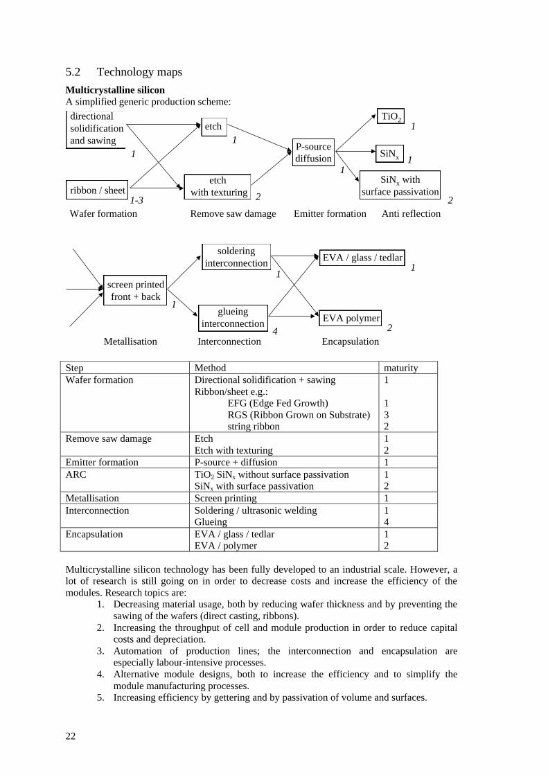
5.2 Technology maps
Multicrystalline siliconA simplified generic production scheme:
directionalsolidificationand sawing
ribbon / sheet
etch
etch with texturing
P-sourcediffusion
TiO2
SiNx
SiNx withsurface passivation
screen printedfront + back
solderinginterconnection
glueinginterconnection
EVA / glass / tedlar
EVA polymer
Wafer formation Remove saw damage Emitter formation Anti reflection
Metallisation Interconnection Encapsulation
1
1
1-3
1
2
11
1
2
1
1
4 2
Step Method maturityWafer formation Directional solidification + sawing
Ribbon/sheet e.g.:EFG (Edge Fed Growth)RGS (Ribbon Grown on Substrate)string ribbon
1
132
Remove saw damage EtchEtch with texturing
12
Emitter formation P-source + diffusion 1ARC TiO2 SiNx without surface passivation
SiNx with surface passivation12
Metallisation Screen printing 1Interconnection Soldering / ultrasonic welding
Glueing14
Encapsulation EVA / glass / tedlarEVA / polymer
12
Multicrystalline silicon technology has been fully developed to an industrial scale. However, alot of research is still going on in order to decrease costs and increase the efficiency of themodules. Research topics are:
1. Decreasing material usage, both by reducing wafer thickness and by preventing thesawing of the wafers (direct casting, ribbons).
2. Increasing the throughput of cell and module production in order to reduce capitalcosts and depreciation.
3. Automation of production lines; the interconnection and encapsulation areespecially labour-intensive processes.
4. Alternative module designs, both to increase the efficiency and to simplify themodule manufacturing processes.
5. Increasing efficiency by gettering and by passivation of volume and surfaces.
23
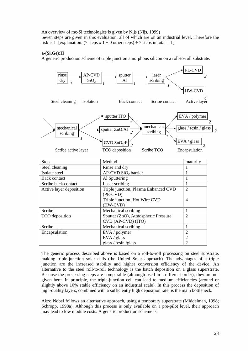
An overview of mc-Si technologies is given by Nijs (Nijs, 1999)Seven steps are given in this evaluation, all of which are on an industrial level. Therefore therisk is 1 [explanation: (7 steps x 1 + 0 other steps) ÷ 7 steps in total = 1].
a-(Si,Ge):HA generic production scheme of triple junction amorphous silicon on a roll-to-roll substrate:
rinsedry
AP-CVDSiO2
sputterAl
laserscribing
PE-CVD
HW-CVD
mechanicalscribing
sputter ITO
sputter ZnO:Al
CVD SnO2:F
mechanicalscribing
EVA / polymer
EVA / glass
Steel cleaning Isolation Back contact Scribe contact Active layer
Scribe active layer TCO deposition Scribe TCO Encapsulation
1 1 1 1
2
4
1
2
2
2
1
2
2
glass / resin / glass2
Step Method maturitySteel cleaning Rinse and dry 1Isolate steel AP-CVD SiO2 barrier 1Back contact Al Sputtering 1Scribe back contact Laser scribing 1Active layer deposition Triple junction, Plasma Enhanced CVD
(PE-CVD)Triple junction, Hot Wire CVD(HW-CVD)
2
4
Scribe Mechanical scribing 1TCO deposition Sputter (ZnO), Atmospheric Pressure
CVD (AP-CVD) (ITO)2
Scribe Mechanical scribing 1Encapsulation EVA / polymer
EVA / glassglass / resin /glass
222
The generic process described above is based on a roll-to-roll processing on steel substrate,making triple-junction solar cells (the United Solar approach). The advantages of a triplejunction are the increased stability and higher conversion efficiency of the device. Analternative to the steel roll-to-roll technology is the batch deposition on a glass superstrate.Because the processing steps are comparable (although used in a different order), they are notgiven here. In principle, the triple-junction cell can lead to medium efficiencies (around orslightly above 10% stable efficiency on an industrial scale). In this process the deposition ofhigh-quality layers, combined with a sufficiently high deposition rate, is the main bottleneck.
Akzo Nobel follows an alternative approach, using a temporary superstrate (Middelman, 1998;Schropp, 1998a). Although this process is only available on a pre-pilot level, their approachmay lead to low module costs. A generic production scheme is:
24
Step Method Maturitytemporary superstrate Al, Cu or steel foil 1TCO deposition SnO2:F 2scribe TCO laser scribing 1active layer deposition double junction PE-CVD 3a
scribe laser scribing 1back contact deposition ZnO Ag/Al 1scribe back contact mechanical scribing 1laminate permanent substrate EVA / polymer 2remove superstrate etching 4encapsulation EVA / polymer 2a: maturity score 3 because of the width of over 1 metre in Helianthos.
Schropp (1998) and Caymax (1994) give an overview of the a-(Si,Ge):H technology. The lowerrisk value for a-(Si,Ge):H is ({6 industrial steps * 1 + 3 pilot steps * 2} / 9 steps) = 1.3. Thehigher value is (1.3 + [3 pilot steps * 2 / 10]) = 1.9.For the Helianthos route the risk value is 2.1 - 3.7
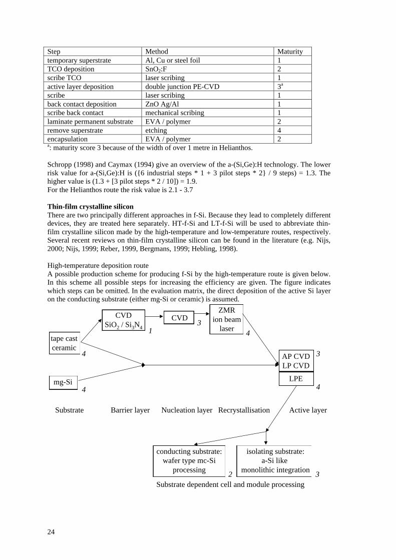
Thin-film crystalline siliconThere are two principally different approaches in f-Si. Because they lead to completely differentdevices, they are treated here separately. HT-f-Si and LT-f-Si will be used to abbreviate thin-film crystalline silicon made by the high-temperature and low-temperature routes, respectively.Several recent reviews on thin-film crystalline silicon can be found in the literature (e.g. Nijs,2000; Nijs, 1999; Reber, 1999, Bergmans, 1999; Hebling, 1998).
High-temperature deposition routeA possible production scheme for producing f-Si by the high-temperature route is given below.In this scheme all possible steps for increasing the efficiency are given. The figure indicateswhich steps can be omitted. In the evaluation matrix, the direct deposition of the active Si layeron the conducting substrate (either mg-Si or ceramic) is assumed.
tape castceramic
mg-Si
CVDSiO2 / Si3N4
CVD ZMR
ion beamlaser
AP CVDLP CVD
LPE
Substrate Barrier layer Nucleation layer Recrystallisation Active layer
4
4
4
4
3
3
conducting substrate:wafer type mc-Si
processing
isolating substrate:a-Si like
monolithic integration
Substrate dependent cell and module processing
1
2 3
25
Step Method MaturitySubstrate Ceramic tape casting
Metallurgical grade Si44
Barrier layer Optional in some routes; CVD of SiO2,Si3N4
1
Nucleation layer Optional in some routes, Si CVD 3Recrystallisation Optional in some routes, Zone Melting
Recrystallisation (ZMR), laserrecrystallisation , ion beamrecrystallisation
4
Active layer deposition AP-CVD or Low Pressure CVD(LP-CVD)LPE (Liquid Phase Epitaxy)
3
4Cell processing Depends on device design
for conducting substrate:emitter formation (diffusion)ARC (TiO2, SiNx)metallisation (screen printing)
2
Interconnection Depends on device design, monolithicintegration or soldering
2 / 3
Encapsulation EVA / glassEVA / polymer
14
From the above generic production scheme it is obvious that high-temperature film silicon onlyexists on a laboratory level. Although some techniques are available on an industrial level (e.g.tape casting of ceramics), either the material itself has to be developed (e.g. which ceramicmaterial) or the technique does not yet meet the desired throughput (e.g. Si CVD). Because it isnot yet clear how the final device will look, some of the processing steps given here areoptional, in order to increase the efficiency of the device. These additional steps will alsoincrease the production cost. Once f-Si is on a pilot-line level, it may benefit from the existenceof available industrial mc-Si production technology. If the (initial) HT-f-Si is based on a wafertype conducting substrate with an active layer on top, processing may be relatively simple in theexisting mc-Si production lines.
Research on high-temperature film silicon has a long history, but the progress has (thus far)been only limited (Poortmans, 2000). If this route does not show promising results within thenext couple of years (e.g. laboratory cells on cheap substrate with an efficiency in the range of15%) it is questionable whether or not it will be useful to develop it further (Glasgow, 2000).From the table above, the calculated risk is 3.0 - 4.4.
26
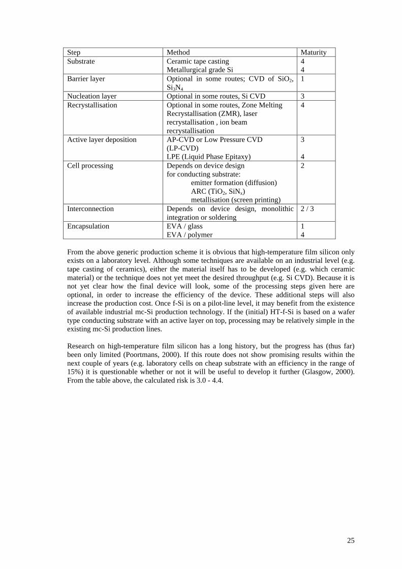
Low-temperature deposition routeA possible production scheme is given below. A glass superstrate is assumed.
rinsescribebreak
laserscribing
PE-CVD
HW-CVD
mechanicalscribing
sputter ITO
sputter ZnO:Al
CVD SnO2:F
mechanicalscribing
EVA / polymer
EVA / glass
Glass cleaning TCO deposition Scribe TCO Active layer
Scribe active layer Back contact Scribe contact Encapsulation
11
4
2
2
2
1
2
2
LP-CVD4
4
sputterAl
11
Step Method MaturityGlass cutting and cleaning Rinse, scribe and break 1TCO deposition Sputter, AP-CVD 2scribing Laser scribing 1Active layer deposition Si CVD (PE-CVD, LP-CVD, HW-CVD) 4Scribing Mechanical scribing 1Back contact Metal sputtering 1Scribing Mechanical scribing 1Encapsulation EVA / glass
EVA / polymer22
The low-temperature route is based on the amorphous silicon approach, but the silicon isdeposited as nano- or microcrystalline silicon. Although nice results have been obtained on alaboratory level (10% by Neuchatel; Shah, 1997), the main bottleneck is scaling up thedeposition. In the laboratory, high-vacuum systems are used and (very) low growth rates areaccepted. However, neither is preferable on an industrial level. Also, the use of fine-grainedmaterial probably limits the efficiency of the devices. Low temperature f-Si remains aninteresting option, because it is expected that fully stable devices can be produced.From the table above, the risk is 1.6 - 2.6
27
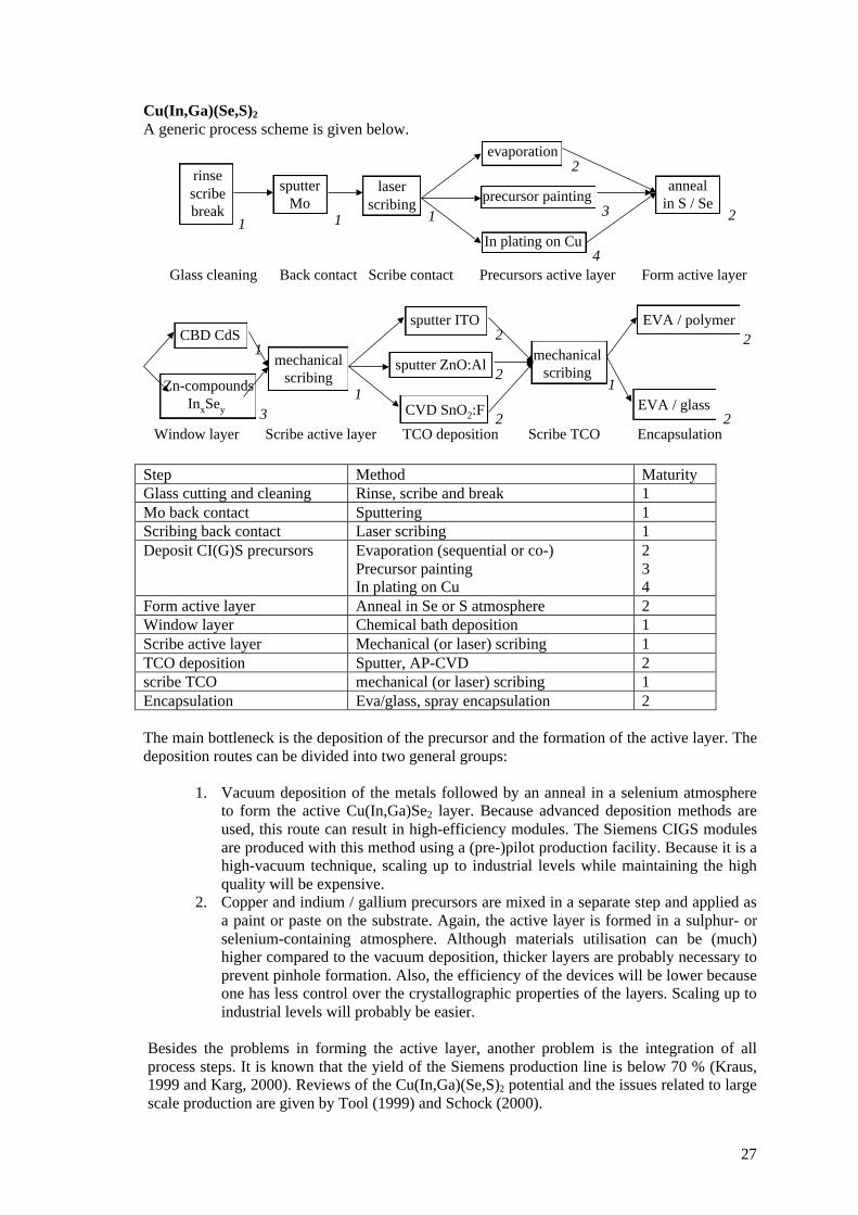
Cu(In,Ga)(Se,S)2
A generic process scheme is given below.
rinsescribebreak
laserscribing
evaporation
In plating on Cu
annealin S / Se
sputter ITO
sputter ZnO:Al
CVD SnO2:F
mechanicalscribing
EVA / polymer
EVA / glass
Glass cleaning Back contact Scribe contact Precursors active layer Form active layer
Window layer Scribe active layer TCO deposition Scribe TCO Encapsulation
1 1
4
2
2
2
1
2
2
precursor painting3
2sputter
Mo
1
2
CBD CdS
Zn-compoundsInxSey 3
1
mechanicalscribing
1
Step Method MaturityGlass cutting and cleaning Rinse, scribe and break 1Mo back contact Sputtering 1Scribing back contact Laser scribing 1Deposit CI(G)S precursors Evaporation (sequential or co-)
Precursor paintingIn plating on Cu
234
Form active layer Anneal in Se or S atmosphere 2Window layer Chemical bath deposition 1Scribe active layer Mechanical (or laser) scribing 1TCO deposition Sputter, AP-CVD 2scribe TCO mechanical (or laser) scribing 1Encapsulation Eva/glass, spray encapsulation 2
The main bottleneck is the deposition of the precursor and the formation of the active layer. Thedeposition routes can be divided into two general groups:
1. Vacuum deposition of the metals followed by an anneal in a selenium atmosphereto form the active Cu(In,Ga)Se2 layer. Because advanced deposition methods areused, this route can result in high-efficiency modules. The Siemens CIGS modulesare produced with this method using a (pre-)pilot production facility. Because it is ahigh-vacuum technique, scaling up to industrial levels while maintaining the highquality will be expensive.
2. Copper and indium / gallium precursors are mixed in a separate step and applied asa paint or paste on the substrate. Again, the active layer is formed in a sulphur- orselenium-containing atmosphere. Although materials utilisation can be (much)higher compared to the vacuum deposition, thicker layers are probably necessary toprevent pinhole formation. Also, the efficiency of the devices will be lower becauseone has less control over the crystallographic properties of the layers. Scaling up toindustrial levels will probably be easier.
Besides the problems in forming the active layer, another problem is the integration of allprocess steps. It is known that the yield of the Siemens production line is below 70 % (Kraus,1999 and Karg, 2000). Reviews of the Cu(In,Ga)(Se,S)2 potential and the issues related to largescale production are given by Tool (1999) and Schock (2000).
28
From the table above, the risk is 1.4 - 2.2
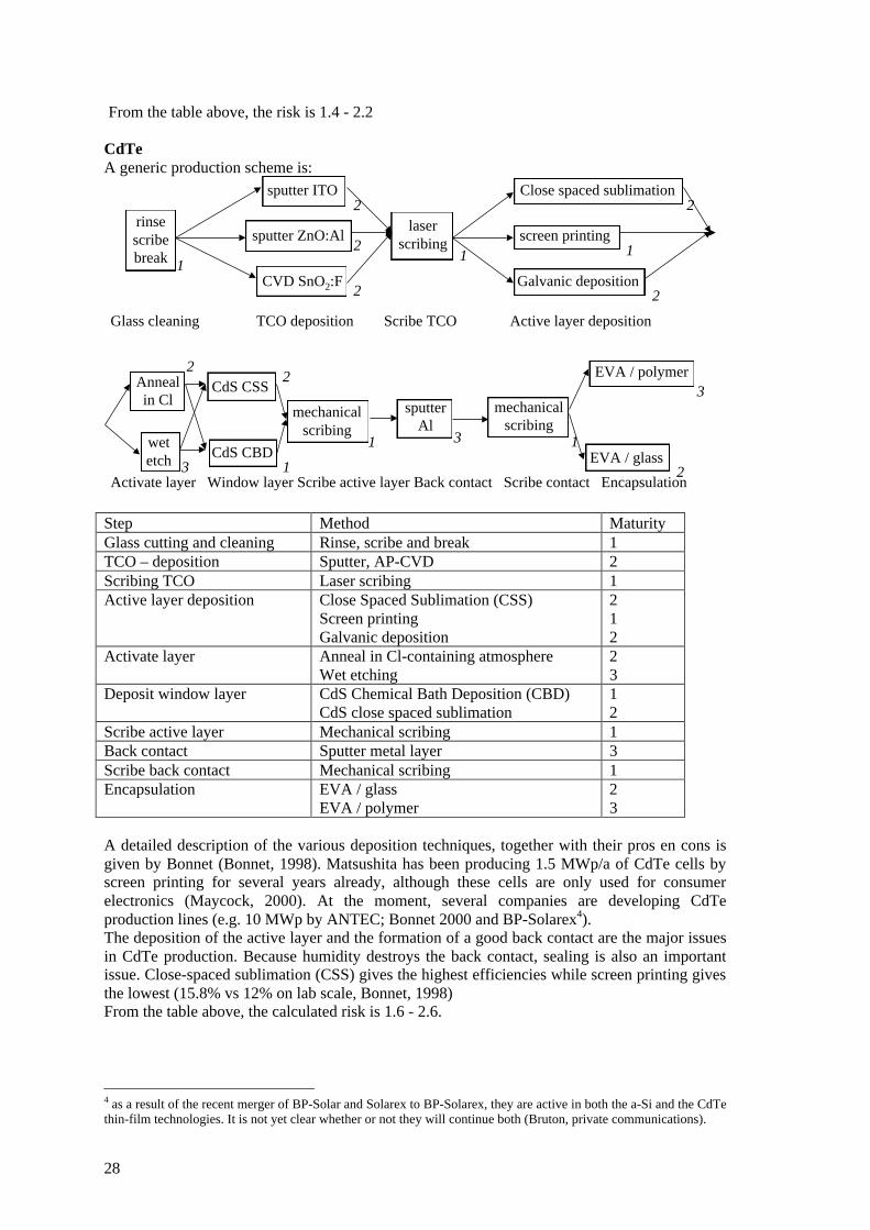
CdTeA generic production scheme is:
rinsescribebreak
laserscribing
Close spaced sublimation
Galvanic deposition
mechanicalscribing
sputter ITO
sputter ZnO:Al
CVD SnO2:F
mechanicalscribing
EVA / polymer
EVA / glass
Glass cleaning TCO deposition Scribe TCO Active layer deposition
Activate layer Window layer Scribe active layer Back contact Scribe contact Encapsulation
11
2
2
2
2
1
3
2
screen printing1
2
sputterAl
31
Annealin Cl
wetetch
CdS CSS
CdS CBD3
2
1
2
Step Method MaturityGlass cutting and cleaning Rinse, scribe and break 1TCO – deposition Sputter, AP-CVD 2Scribing TCO Laser scribing 1Active layer deposition Close Spaced Sublimation (CSS)
Screen printingGalvanic deposition
212
Activate layer Anneal in Cl-containing atmosphereWet etching
23
Deposit window layer CdS Chemical Bath Deposition (CBD)CdS close spaced sublimation
12
Scribe active layer Mechanical scribing 1Back contact Sputter metal layer 3Scribe back contact Mechanical scribing 1Encapsulation EVA / glass
EVA / polymer23
A detailed description of the various deposition techniques, together with their pros en cons isgiven by Bonnet (Bonnet, 1998). Matsushita has been producing 1.5 MWp/a of CdTe cells byscreen printing for several years already, although these cells are only used for consumerelectronics (Maycock, 2000). At the moment, several companies are developing CdTeproduction lines (e.g. 10 MWp by ANTEC; Bonnet 2000 and BP-Solarex4).The deposition of the active layer and the formation of a good back contact are the major issuesin CdTe production. Because humidity destroys the back contact, sealing is also an importantissue. Close-spaced sublimation (CSS) gives the highest efficiencies while screen printing givesthe lowest (15.8% vs 12% on lab scale, Bonnet, 1998)From the table above, the calculated risk is 1.6 - 2.6.
4 as a result of the recent merger of BP-Solar and Solarex to BP-Solarex, they are active in both the a-Si and the CdTethin-film technologies. It is not yet clear whether or not they will continue both (Bruton, private communications).
29
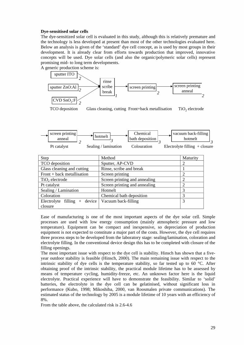
Dye-sensitised solar cellsThe dye-sensitized solar cell is evaluated in this study, although this is relatively premature andthe technology is less developed at present than most of the other technologies evaluated here.Below an analysis is given of the ‘standard’ dye cell concept, as is used by most groups in theirdevelopment. It is already clear from efforts towards production that improved, innovativeconcepts will be used. Dye solar cells (and also the organic/polymeric solar cells) representpromising mid- to long term developments.A generic production scheme is:
sputter ITO
sputter ZnO:Al
CVD SnO2:F
2
2
2
rinsescribebreak
screen printing screen printinganneal
screen printinganneal hotmelt
Chemical bath deposition
vacuum back-fillinghotmelt
TCO deposition Glass cleaning, cutting Front+back metallisation TiO2 electrode
Pt catalyst Sealing / lamination Colouration Electrolyte filling + closure
12
2
2 3 3 3
Step Method MaturityTCO deposition Sputter, AP-CVD 2Glass cleaning and cutting Rinse, scribe and break 1Front + back metallisation Screen printing 2TiO2 electrode Screen printing and annealing 2Pt catalyst Screen printing and annealing 2Sealing / Lamination Hotmelt 3Coloration Chemical bath deposition 3Electrolyte filling + deviceclosure
Vacuum back-filling 3
Ease of manufacturing is one of the most important aspects of the dye solar cell. Simpleprocesses are used with low energy consumption (mainly atmospheric pressure and lowtemperature). Equipment can be compact and inexpensive, so depreciation of productionequipment is not expected to constitute a major part of the costs. However, the dye cell requiresthree process steps to be developed from the laboratory stage: sealing/lamination, coloration andelectrolyte filling. In the conventional device design this has to be completed with closure of thefilling openings.The most important issue with respect to the dye cell is stability. Hinsch has shown that a five-year outdoor stability is feasible (Hinsch, 2000). The main remaining issue with respect to theintrinsic stability of dye cells is the temperature stability, so far tested up to 60 °C. Afterobtaining proof of the intrinsic stability, the practical module lifetime has to be assessed bymeans of temperature cycling, humidity-freeze, etc. An unknown factor here is the liquidelectrolyte. Practical experience will have to demonstrate the feasibility. Similar to ‘solid’batteries, the electrolyte in the dye cell can be gelatinised, without significant loss inperformance (Kubo, 1998; Mikoshiba, 2000, van Roosmalen private communications). Theestimated status of the technology by 2005 is a module lifetime of 10 years with an efficiency of8%.From the table above, the calculated risk is 2.6-4.6
30
Organic solar-cell devicesThis discussion on alternative organic solar-cell devices has a time horizon that exceeds 2005.
Organic/polymeric solar cells are by many considered to have a high potential, in terms of costand possibly in terms of efficiency. This is related to the fact that they are based on the use oflow cost materials or on the use of very small quantities of more expensive materials. Also theprocesses used for device fabrication are (expected or demonstrated to be) suitable for low-cost,large-scale, large area manufacturing. Ideally, high-efficiency organic/polymeric cells can beapplied at temperatures compatible with almost any surface or substrate, using atmosphericpressure techniques and environmentally benign materials (Roosmalen, 2000). In spite of themany fundamental questions that still exist, this perspective, and the fact that exploration hasonly just begun, causes a strong driving force to develop this type of solar cells.The principal fields of research concern, a.o., the following topics:
- device design, both on a molecular level and on a macroscopic level;- chemical stability of the active materials, in their interaction with light and with other
materials and molecules (including those unintentionally built in during manufacturingor diffused in through the encapsulant);
- stability of the molecular structures used (e.g. phase separation);- charge transport and collection;- device modelling and understanding;- deposition/manufacturing techniques suitable for high efficiency and/or high-
throughput;- encapsulation (related to the question whether the active part of the devices should be
closed on a molecular level, or made compatible with indiffusing species).
A multitude of approaches is followed, which reflects the possibilities in terms of deviceconcepts, materials use and materials engineering (molecular design). Apart from the sensitisedoxides mentioned earlier, they can be divided roughly into two other categories, flat-layersystems and bulk heterojunctions. Typical exponents of the flat-layer systems are the organicp/n junctions as investigated by Meissner (Meissner, 2000) and Tang (Tang, 1986) and theantenna concept (WAU, 2000).
Several approaches are being followed to transform the liquid-containing dye solar cell intosolid-state devices, replacing the liquid electrolyte with solid hole conductors. Bach (Bach,1998) replaced the liquid electrolyte by an amorphous molecular hole conductor (spiro-compound, OMeTAD). Tennakone (Tennakone, 1995.) and O’Regan (personalcommunications) replaced the liquid electrolyte by an inorganic hole conducting salt (CuI,CuSCN) while maintaining an organic-based dye. Salafsky (Salafsky, 1998; Christiaans, 1999;Hal, 1999) combine the function of light absorption (dye) and hole conduction in a singlepolymeric phase, where MEH-PPV and polythiophene are used as polymers. Several attemptshave also been made to replace all organic components with inorganic ones, such as in the ETA(extremely thin absorber), in which for instance CuInS2 can be used as the dye and an inorganicsalt (CuI, CuSCN) can be used as the hole conductor (Möller, 1998).
Likewise, several attempts have been made to obtain bulk heterojunction or interpenetratingnetwork organic/polymeric solar cells. The most well known is the polymer (MEH-PPV)/modified C60 device, introduced by the Heeger group (Yu, 1995). The molecular organicC60 material and the polymer are spin-coated in a single layer but form two interpenetratingnetworks that form a bulk heterojunction, this way functioning as a solar cells. Following this,the route of interpenetrating networks of two polymeric materials is also pursued. The Friendgroup (Petritsch, 1998) realised this by laminating the two polymeric layers on top of eachother, a treatment that resulted in (partial) intermixing. Transforming a single, crystallineorganic molecular material (pentacene) into a bulk heterojunction by doping the materialforming doped and non-doped phase regions of interpenetrating networks is another approachthat was recently reported by Lucent Technologies (Schön, 2000; Schön, 2000a).
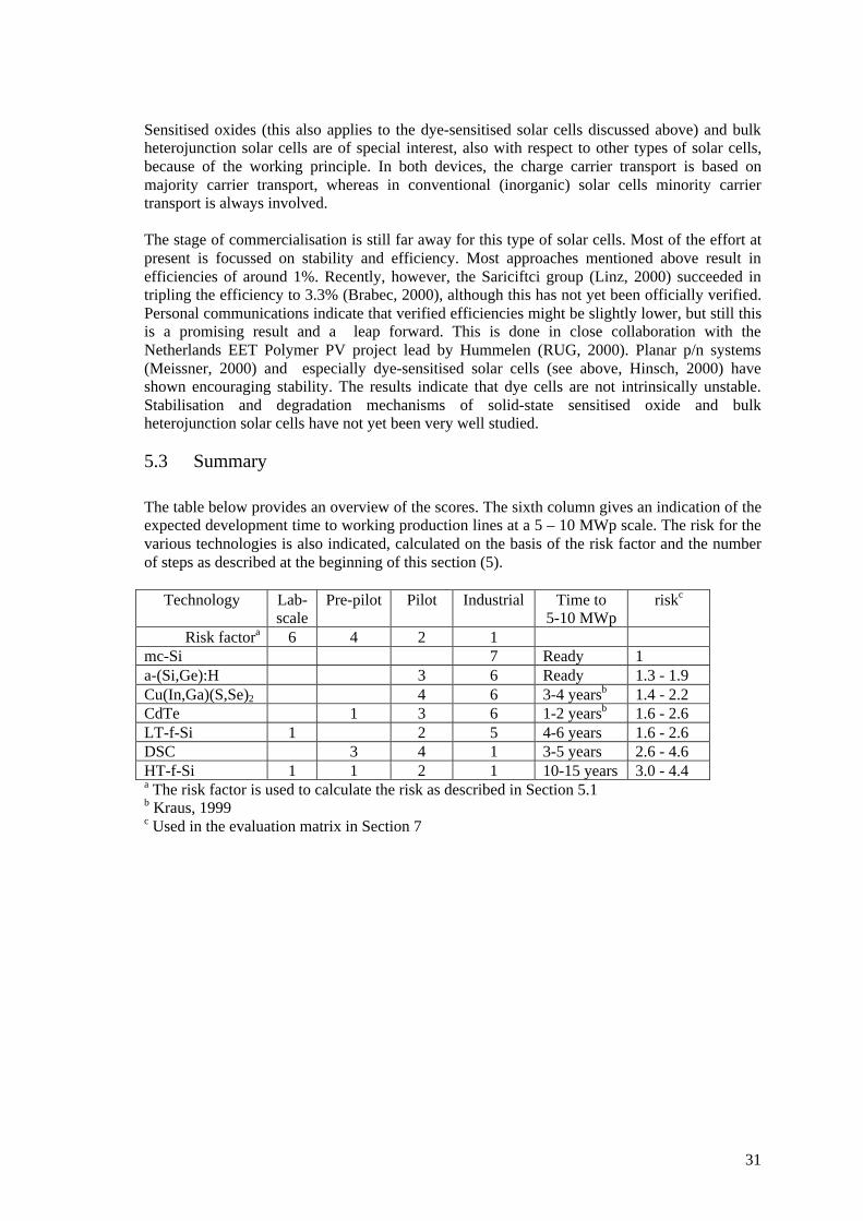
31
Sensitised oxides (this also applies to the dye-sensitised solar cells discussed above) and bulkheterojunction solar cells are of special interest, also with respect to other types of solar cells,because of the working principle. In both devices, the charge carrier transport is based onmajority carrier transport, whereas in conventional (inorganic) solar cells minority carriertransport is always involved.
The stage of commercialisation is still far away for this type of solar cells. Most of the effort atpresent is focussed on stability and efficiency. Most approaches mentioned above result inefficiencies of around 1%. Recently, however, the Sariciftci group (Linz, 2000) succeeded intripling the efficiency to 3.3% (Brabec, 2000), although this has not yet been officially verified.Personal communications indicate that verified efficiencies might be slightly lower, but still thisis a promising result and a leap forward. This is done in close collaboration with theNetherlands EET Polymer PV project lead by Hummelen (RUG, 2000). Planar p/n systems(Meissner, 2000) and especially dye-sensitised solar cells (see above, Hinsch, 2000) haveshown encouraging stability. The results indicate that dye cells are not intrinsically unstable.Stabilisation and degradation mechanisms of solid-state sensitised oxide and bulkheterojunction solar cells have not yet been very well studied.
5.3 Summary
The table below provides an overview of the scores. The sixth column gives an indication of theexpected development time to working production lines at a 5 – 10 MWp scale. The risk for thevarious technologies is also indicated, calculated on the basis of the risk factor and the numberof steps as described at the beginning of this section (5).
Technology Lab-scale
Pre-pilot Pilot Industrial Time to5-10 MWp
riskc
Risk factora 6 4 2 1mc-Si 7 Ready 1a-(Si,Ge):H 3 6 Ready 1.3 - 1.9Cu(In,Ga)(S,Se)2 4 6 3-4 yearsb 1.4 - 2.2CdTe 1 3 6 1-2 yearsb 1.6 - 2.6LT-f-Si 1 2 5 4-6 years 1.6 - 2.6DSC 3 4 1 3-5 years 2.6 - 4.6HT-f-Si 1 1 2 1 10-15 years 3.0 - 4.4a The risk factor is used to calculate the risk as described in Section 5.1b Kraus, 1999c Used in the evaluation matrix in Section 7
32
6. LITERATURE REVIEW FOR COST AND SUSTAINABILITY
Unless otherwise stated, this literature review contains data for the expected situation in 2005.
6.1 Module production costs
Unless stated otherwise, the module production costs given here are the basic production costs,not including overhead costs such as marketing and sales. The module production costs aregiven in €/Wp. All data are derived from the literature described below. The efficiency differsbetween the studies. We corrected for this variance by choosing a fixed efficiency for eachtechnology. The dollar ($) and the euro (€) are assumed to be of equal value.
Multicrystalline siliconThe costs for crystalline silicon modules is estimated to be between 0.88 €/Wp and 1.22 €/Wpwith an efficiency of 16%. Frantzis (2000) reports a value of 1.15 $/Wp for the year 2010. Thismodule has an efficiency of 17% at a production scale of 100 MWp. The MusicFM study (BPSolar, 1996) gives costs of 0.91 €/Wp at an efficiency of 15.5%. A 500 MWp plant was used inthat report.
a-(Si,Ge):HAmorphous-silicon solar modules with an efficiency of 10% will cost between 0.55 €/Wp and0.75 €/Wp. The first value is derived from the BP Solar (1996) report. For a 60 MWp plantamorphous-silicon solar cells with 8% efficiency can be produced for 0.69 €/Wp. Maycock(2000) reports the expectation that a 10 MWp plant will be able to produce a 10% efficientmodule at 0.75 €/Wp near the year 2005.The target for the module costs in the Helianthos project is 0.5 €/Wp. This target must bereached by a roll to roll production at a sufficiently high yield (Middelman, 1998).
Thin-film crystalline siliconThe only cost calculation for thin-film crystalline silicon gives a figure of 0.78 €/Wp (Tool,1998). This calculation is based on a high-temperature production route, that is fully automated.The modules produced will have an efficiency of 16%. Assuming a 14% efficiency, theproduction costs of HT-f-Si will be 0.98 €/Wp.No data are available for the low-temperature f-Si route. This route is comparable to the a-Sitechnology, although additional efforts on e.g. light trapping will be important. However, forthis evaluation the costs for low-temperature f-Si are assumed to be comparable to a-(Si,Ge):H.
Cu(In,Ga)(Se,S)2
The costs for CIS modules vary from 0.7 €/Wp to 0.94 €/Wp for an efficiency of 12%. Kapur(1997) states the value of 0.94 €/Wp for the production in a 16 MWp plant. In the MusicFMstudy the cost is 0.70 €/Wp in a 60 MWp plant.
CdTeFrom MusicFM (BP Solar, 1996) cadmium-telluride solar cells with an efficiency of 12% canbe produced for 0.72 €/Wp in a 60 MWp plant. For an efficiency of 10% the cost would be 0.86€/Wp. Frantzis (2000) reports module production costs of 0.95 €/Wp at an efficiency of 13%for a 100 MWp plant. This gives costs of 1.24 €/Wp at an efficiency of 10%.
Dye-sensitised cellGrätzel (1994), referring to a study of the Research Triangle Institute, reports the value of 0.6€/Wp for a 10 MWp production scale. No background information on this figure is known.
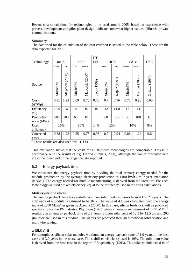
33
Recent cost calculations for technologies to be used around 2005, based on experience withprocess development and pilot-plant design, indicate somewhat higher values. (Hinsch, privatecommunication).
SummaryThe data used for the calculation of the cost criterion is stated in the table below. These are thedata expected for 2005.
Technology mc-Si a-SiaHT-f-Si CIGS CdTe DSC
min max min max min max min max
Source
Mus
icFM
May
cock
(20
00)
Mus
icFM
May
cock
(20
00)
Too
l (19
99)
Mus
icFM
Kap
ur (
1997
)
Mus
icFM
Fran
zis
(200
0)
Grä
ztel
(19
94)
Costs(€/Wp)
0.91 1.22 0.69 0.75 0.76 0.7 0.96 0.72 0.95 0.60
Efficiency(%)
15.5 16 8 10 16 12 11.8 12 13
Productionscale (MW)
500 100 60 10 60 16 60 100 10
Usedefficiency
16% 10% 14% 12% 10% 8%
Correctedcosts
0.88 1.22 0.55 0.75 0.98 0.7 0.94 0.86 1.24 0.6
a These results are also used for LT-f-Si
This evaluation shows that the costs for all thin-film technologies are comparable. This is inaccordance with the results of e.g. Franzis (Franzis, 2000), although the values presented hereare at the lower end of the range that she reported.
6.2 Energy payback time
We calculated the energy payback time by dividing the total primary energy needed for themodule production by the average electricity production at 1100 kWh / m2 / year irradiation(KNMI). The energy needed for module manufacturing is derived from the literature. For eachtechnology we used a fixed efficiency, equal to the efficiency used in the costs calculations.
Multicrystalline siliconThe energy payback time for crystalline-silicon solar modules varies from 4.1 to 2.3 years. Theefficiency of a module is assumed to be 16%. The value of 4.1 was calculated from the energyinput of 2600 MJ/m2 as given by Alsema (2000). In this case, silicon feedstock will be producedspecifically for the PV industry. Phylipsen (1995) gives an energy requirement of 1440 MJ/m2,resulting in an energy payback time of 2.3 years. Silicon solar cells of 12.5 by 12.5 cm and 200µm thick are used in this module. The wafers are produced through directional solidification andmultiwire sawing.
a-(Si,Ge):HFor amorphous silicon solar modules we found an energy payback time of 1.9 years in the bestcase and 3.0 years in the worst case. The stabilised efficiency used is 10%. The minimum valueis derived from the base case in the report of Engelenburg (1993). This solar module consists of
34
a tandem silicon layer (a-Si:H) deposited on a glass substrate. The back of the module is alsoencapsulated with a glass layer. Both glass plates are 2 mm thick.Alsema (2000) reported the worst-case figure (1200 MJ/m2) by comparing several energystudies on amorphous silicon. The encapsulation materials used determine a major part of theenergy requirement of amorphous silicon modules. In this case, a glass/glass encapsulation isused. Alsema also reports that a polymer back cover reduces the energy requirements by 150MJ/m2.
We calculated the energy payback time for a roll-to-roll amorphous silicon technology as beingresearched in the Heliantos project (Middelman, 1998; Schropp, 1998a). For the basic celldesign and cell processing we used the data from Engelburg (1993). The cells are processed ona temporary substrate of 50 µm thick aluminium foil. Then the back cover of PMMA of 0.5 mm
is laminated with a 50 µm thick layer of EVA. The aluminium substrate is removed in a wetetching step with hydrochloric acid. Finally, the front cover is laminated in the same way as theback cover. The energy requirement for this process is 740 MJ/m2, which is equal to normalamorphous silicon technology. The objective of the Helianthos project is to manufacturemodules with an efficiency of 5%. This will lead to an energy payback time of 3.7 years.
Thin film-crystalline siliconNo exact data on the energy use during the production of thin-film crystalline silicon on glassare known. Because the production route, the efficiency and the technical lifetime are allcomparable to those of amorphous silicon, and the energy payback time is expected to becomparable too.As information is also lacking for HT-f-Si, we have used the energy input of mc-Si. Because thesubstrate production probably requires a high temperature, the highest estimated value for mc-Siis taken. Together with an efficiency of 14%, this gives an energy payback time of 4.7 years.
Cu(In,Ga)(Se,S)2
The energy payback time of CIGS modules is derived from the study of Alsema (1992) due tothe lack of more recent data. His base case resulted in a payback time of 1.8 and the best case in1.3 years. The design of both solar cells is similar. The main difference lies in the choice of theencapsulation materials, which are two glass plates in the base case and glass/plasticencapsulation in the best case. A future scenario for energy use during the production of glass isalso taken into account for the best case. A further difference stems from the assumptions madefor the energy requirements for the production of the capital goods. The efficiency is set at 12%.
CdTeThe energy payback time of CdTe solar modules is the lowest of all evaluated technologies,namely between 0.5 and 0.9 years. These figures are calculated from the same report we usedfor CIGS (Alsema, 1992).
Dye-sensitised solar cellsThe energy payback time for the organic dye-sensitised solar module is calculated to be 1 year.A range cannot be given because only one internal ECN document was available (Ruseler,1999). As the data in this report are derived from a laboratory production process, it can beexpected that the energy payback time will decrease on an industrial production scale. However,since the energy requirement is dominated by the used glass substrate (about 60%) it is likelythat the energy requirement will not decrease by more than 20 to 30%. The efficiency for thisorganic cell is estimated to be 8%.
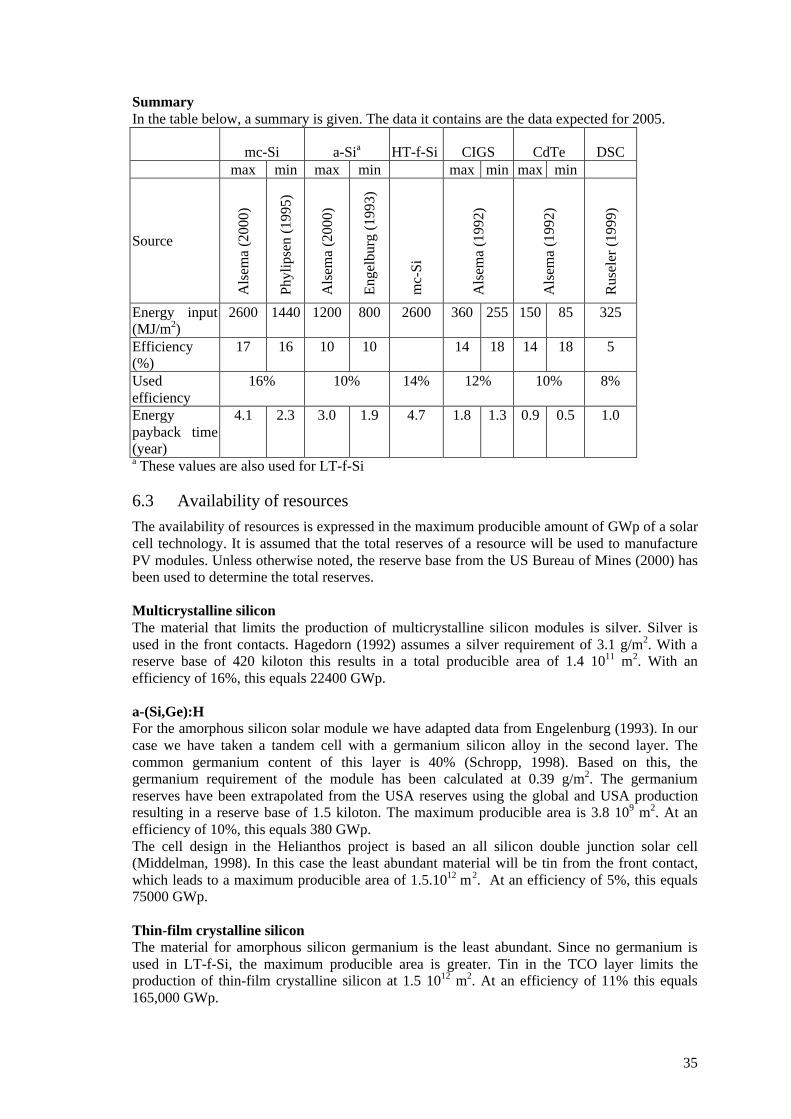
35
SummaryIn the table below, a summary is given. The data it contains are the data expected for 2005.
mc-Si a-Sia HT-f-Si CIGS CdTe DSCmax min max min max min max min
SourceA
lsem
a (2
000)
Phyl
ipse
n (1
995)
Als
ema
(200
0)
Eng
elbu
rg (
1993
)
mc-
Si
Als
ema
(199
2)
Als
ema
(199
2)
Rus
eler
(19
99)
Energy input(MJ/m2)
2600 1440 1200 800 2600 360 255 150 85 325
Efficiency(%)
17 16 10 10 14 18 14 18 5
Usedefficiency
16% 10% 14% 12% 10% 8%
Energypayback time(year)
4.1 2.3 3.0 1.9 4.7 1.8 1.3 0.9 0.5 1.0
a These values are also used for LT-f-Si
6.3 Availability of resources
The availability of resources is expressed in the maximum producible amount of GWp of a solarcell technology. It is assumed that the total reserves of a resource will be used to manufacturePV modules. Unless otherwise noted, the reserve base from the US Bureau of Mines (2000) hasbeen used to determine the total reserves.
Multicrystalline siliconThe material that limits the production of multicrystalline silicon modules is silver. Silver isused in the front contacts. Hagedorn (1992) assumes a silver requirement of 3.1 g/m2. With areserve base of 420 kiloton this results in a total producible area of 1.4 1011 m2. With anefficiency of 16%, this equals 22400 GWp.
a-(Si,Ge):HFor the amorphous silicon solar module we have adapted data from Engelenburg (1993). In ourcase we have taken a tandem cell with a germanium silicon alloy in the second layer. Thecommon germanium content of this layer is 40% (Schropp, 1998). Based on this, thegermanium requirement of the module has been calculated at 0.39 g/m2. The germaniumreserves have been extrapolated from the USA reserves using the global and USA productionresulting in a reserve base of 1.5 kiloton. The maximum producible area is 3.8 109 m2. At anefficiency of 10%, this equals 380 GWp.The cell design in the Helianthos project is based an all silicon double junction solar cell(Middelman, 1998). In this case the least abundant material will be tin from the front contact,which leads to a maximum producible area of 1.5.1012 m2. At an efficiency of 5%, this equals75000 GWp.
Thin-film crystalline siliconThe material for amorphous silicon germanium is the least abundant. Since no germanium isused in LT-f-Si, the maximum producible area is greater. Tin in the TCO layer limits theproduction of thin-film crystalline silicon at 1.5 1012 m2. At an efficiency of 11% this equals165,000 GWp.
36
For the high temperature film silicon, a situation comparable to mc-Si is assumed, which meansthe total producible area is 1.4.1011 m2. At an efficiency of 14%, this equals 19600 GWp.
Cu(In,Ga)(Se,S)2
Several studies have been conducted on the resource availability for the CIGS solar module. Allthese studies conclude that indium is the least abundant material. According to Eberspacher(1996) the indium reserves vary between 2.3 and 4.6 kiloton. With an indium requirement of 2.3g/m2, the maximum producible amount is 2.0.109 m2, which corresponds to 240 GWp.According to Alsema (1992), the maximum indium requirement is higher (9.8 g/m2), resultingin a maximum producible area of 4.7 108 m2. At an efficiency of 12%, this equals 56 GWp.
CdTeIn cadmium telluride solar modules tellurium is the least abundant material. Andersson (2000)states a tellurium requirement of 6.5 g/m2. Alsema (1992) reports a tellurium requirement of 8.8g/m2. The total reserve base for tellurium is 38 kiloton, which results in a maximum produciblearea from 3.1 109 to 4.3 109 m2. At an efficiency of 10% this equals from 310 GWp to 430GWp.
Dye-sensitised cellRuthenium is the scarcest material in the dye-sensitised solar cell. Andersson (2000) mentioneda maximum producible area of 6.1010 m2, using a requirement of 0.1 g/m2 and a reserve of 6kiloton (equivalent to 4800 GWp). Ruseler (1999) stated a maximum producible area of 7.1010
m2 or 5600 GWp using a requirement of 22 mg and a reserve of 1.6 kiloton. At an efficiency of8%, this equals 5640 GWp. Both the reserves and requirements mentioned in these sourcesdiffer a lot. This may have something to do with the cell design and the availability of exact dataon ruthenium reserves.
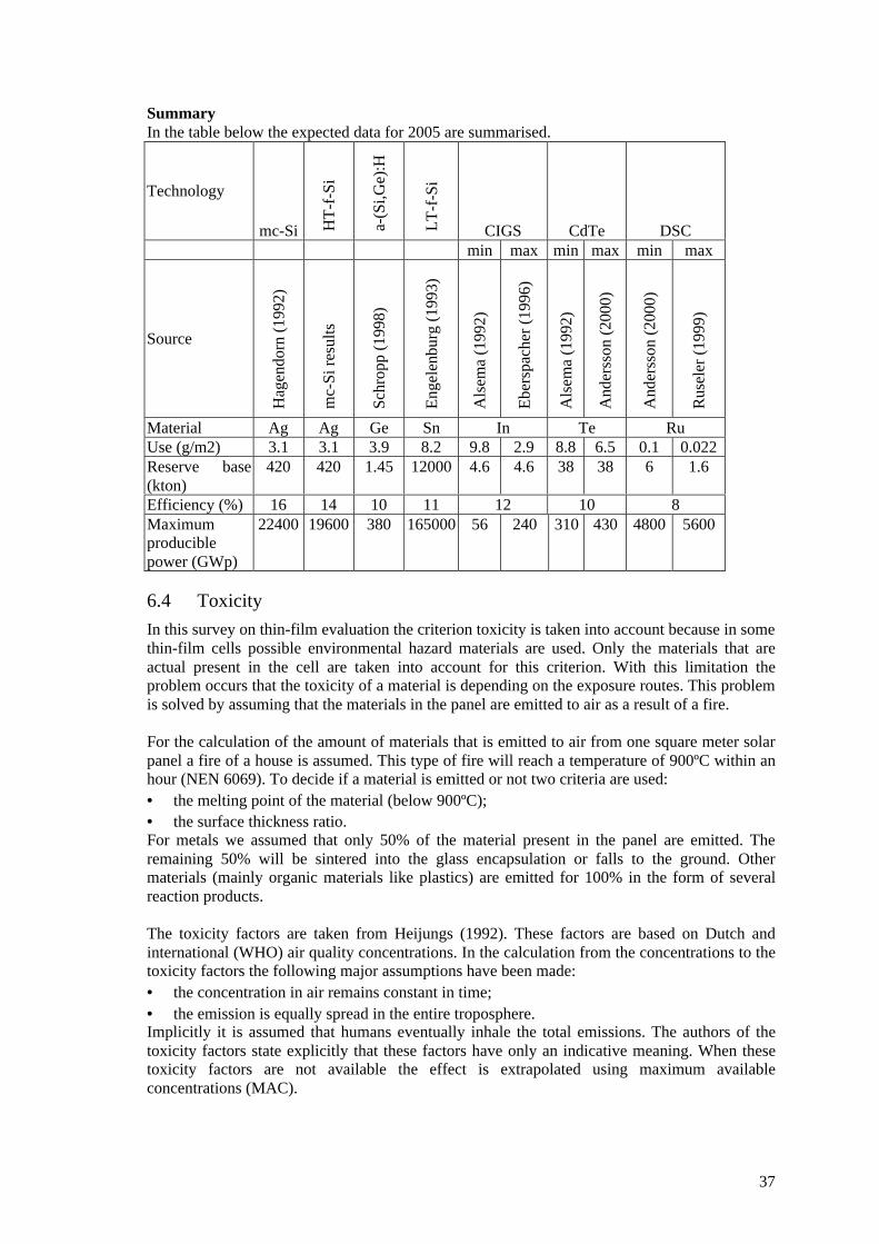
37
SummaryIn the table below the expected data for 2005 are summarised.
Technology
mc-Si HT
-f-S
i
a-(S
i,Ge)
:H
LT
-f-S
i
CIGS CdTe DSCmin max min max min max
Source
Hag
endo
rn (
1992
)
mc-
Si r
esul
ts
Schr
opp
(199
8)
Eng
elen
burg
(19
93)
Als
ema
(199
2)
Ebe
rspa
cher
(19
96)
Als
ema
(199
2)
And
erss
on (
2000
)
And
erss
on (
2000
)
Rus
eler
(19
99)
Material Ag Ag Ge Sn In Te RuUse (g/m2) 3.1 3.1 3.9 8.2 9.8 2.9 8.8 6.5 0.1 0.022Reserve base(kton)
420 420 1.45 12000 4.6 4.6 38 38 6 1.6
Efficiency (%) 16 14 10 11 12 10 8Maximumproduciblepower (GWp)
22400 19600 380 165000 56 240 310 430 4800 5600
6.4 Toxicity
In this survey on thin-film evaluation the criterion toxicity is taken into account because in somethin-film cells possible environmental hazard materials are used. Only the materials that areactual present in the cell are taken into account for this criterion. With this limitation theproblem occurs that the toxicity of a material is depending on the exposure routes. This problemis solved by assuming that the materials in the panel are emitted to air as a result of a fire.
For the calculation of the amount of materials that is emitted to air from one square meter solarpanel a fire of a house is assumed. This type of fire will reach a temperature of 900ºC within anhour (NEN 6069). To decide if a material is emitted or not two criteria are used:• the melting point of the material (below 900ºC);• the surface thickness ratio.For metals we assumed that only 50% of the material present in the panel are emitted. Theremaining 50% will be sintered into the glass encapsulation or falls to the ground. Othermaterials (mainly organic materials like plastics) are emitted for 100% in the form of severalreaction products.
The toxicity factors are taken from Heijungs (1992). These factors are based on Dutch andinternational (WHO) air quality concentrations. In the calculation from the concentrations to thetoxicity factors the following major assumptions have been made:• the concentration in air remains constant in time;• the emission is equally spread in the entire troposphere.Implicitly it is assumed that humans eventually inhale the total emissions. The authors of thetoxicity factors state explicitly that these factors have only an indicative meaning. When thesetoxicity factors are not available the effect is extrapolated using maximum availableconcentrations (MAC).
38
In formula from:toxicity = ∑ mmetals × 0.5 × TF + ∑ morganics × TF
in which:mmetals is mass of the metals in kg/m2 modulemorganics is mass of the reaction products of burned organic materials in kg/m2 moduleTF is Toxicity Factor in kg body mass
The result of the toxicity criterion can be interpreted as the body mass that is contaminated tothe maximum tolerable limits as a result of a burning of one square meter module. The unit forthe toxicity figures stated in this report is kg body mass / m2 module.
Multicrystalline siliconThe toxicity of one square meter of a multicrystalline silicon module is calculated to be 0.086.This is mainly due to the aluminium in the back foil and the lead from the printing pastes, solderand tabs. The composition of the module is derived from Hagedorn (1992) and that of theprinting pastes from the material safety data sheets for these products (Ferro ElectronicMaterials Division).
a-SiGe:HAmorphous silicon has the lowest toxicity score with 4.8 10-3. The aluminium in the backcontact has the greatest impact. The design of the module is derived from Engelenburg (1993).In the second silicon layer 40% germanium is added (Schropp, 1998). No toxicity data forgermanium were available. Therefore the toxicity data of molybdenum were used as anapproximation.The toxicity of the modules in the Heliantos project is comparable to that of LT-f-Si solar cells.
Thin-film crystalline siliconThe toxicity of thin-film crystalline silicon, from a low-temperature production route, can becompared with that of amorphous silicon. There is a slight difference since no germanium isused. This will lead to a toxicity score of 4.5 10-3.For high-temperature f-Si it is assumed that the substrate will have no influence on the toxicityunder the assumptions made. So, assuming processing comparable to mc-Si, the toxicity alsoequals the mc-Si value, which is 0.086.
Cu(In,Ga)(Se,S)2
For CIGS, the composition described by Alsema (1992) is used. The toxicity score for CIGS is0.47. The main contributions to this score are indium and selenium from the active layer and toa lesser extent cadmium in the window layer.
CdTeAs could be expected, the cadmium-telluride solar module has the highest score for toxicity.The score of 2.5 is divided between cadmium and telluride in the proportion 2 to 1. For thecomposition we used the design given in Alsema (1992).
Dye-sensitised solar cellFor the dye-sensitised solar cell, the back and the front contacts have the greatest impact on thetoxicity score of 2.1 10-2. A major uncertainty with this technology is the toxicity of ruthenium,because very little data on this material are known, although the first results for the AMES testof the dye are promising (Vries, 2000). Instead of ruthenium the toxicity value of molybdenumis used. Ruthenium then is responsible for 15% of the toxicity score. The composition used isderived from Ruseler (1999).
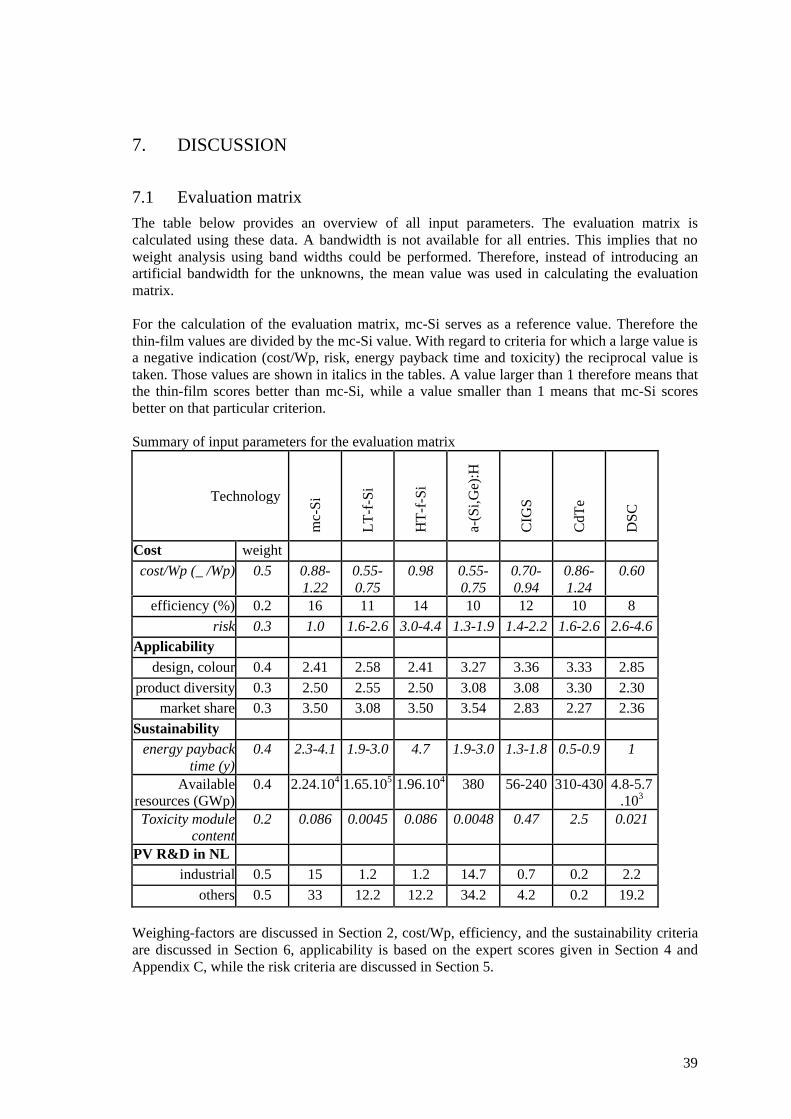
39
7. DISCUSSION
7.1 Evaluation matrix
The table below provides an overview of all input parameters. The evaluation matrix iscalculated using these data. A bandwidth is not available for all entries. This implies that noweight analysis using band widths could be performed. Therefore, instead of introducing anartificial bandwidth for the unknowns, the mean value was used in calculating the evaluationmatrix.
For the calculation of the evaluation matrix, mc-Si serves as a reference value. Therefore thethin-film values are divided by the mc-Si value. With regard to criteria for which a large value isa negative indication (cost/Wp, risk, energy payback time and toxicity) the reciprocal value istaken. Those values are shown in italics in the tables. A value larger than 1 therefore means thatthe thin-film scores better than mc-Si, while a value smaller than 1 means that mc-Si scoresbetter on that particular criterion.
Summary of input parameters for the evaluation matrix
Technology
mc-
Si
LT
-f-S
i
HT
-f-S
i
a-(S
i,Ge)
:H
CIG
S
CdT
e
DSC
Cost weight
cost/Wp (_/Wp) 0.5 0.88-1.22
0.55-0.75
0.98 0.55-0.75
0.70-0.94
0.86-1.24
0.60
efficiency (%) 0.2 16 11 14 10 12 10 8
risk 0.3 1.0 1.6-2.6 3.0-4.4 1.3-1.9 1.4-2.2 1.6-2.6 2.6-4.6Applicability
design, colour 0.4 2.41 2.58 2.41 3.27 3.36 3.33 2.85
product diversity 0.3 2.50 2.55 2.50 3.08 3.08 3.30 2.30market share 0.3 3.50 3.08 3.50 3.54 2.83 2.27 2.36
Sustainabilityenergy payback
time (y)0.4 2.3-4.1 1.9-3.0 4.7 1.9-3.0 1.3-1.8 0.5-0.9 1
Availableresources (GWp)
0.4 2.24.104 1.65.105 1.96.104 380 56-240 310-430 4.8-5.7.103
Toxicity modulecontent
0.2 0.086 0.0045 0.086 0.0048 0.47 2.5 0.021
PV R&D in NLindustrial 0.5 15 1.2 1.2 14.7 0.7 0.2 2.2
others 0.5 33 12.2 12.2 34.2 4.2 0.2 19.2
Weighing-factors are discussed in Section 2, cost/Wp, efficiency, and the sustainability criteriaare discussed in Section 6, applicability is based on the expert scores given in Section 4 andAppendix C, while the risk criteria are discussed in Section 5.
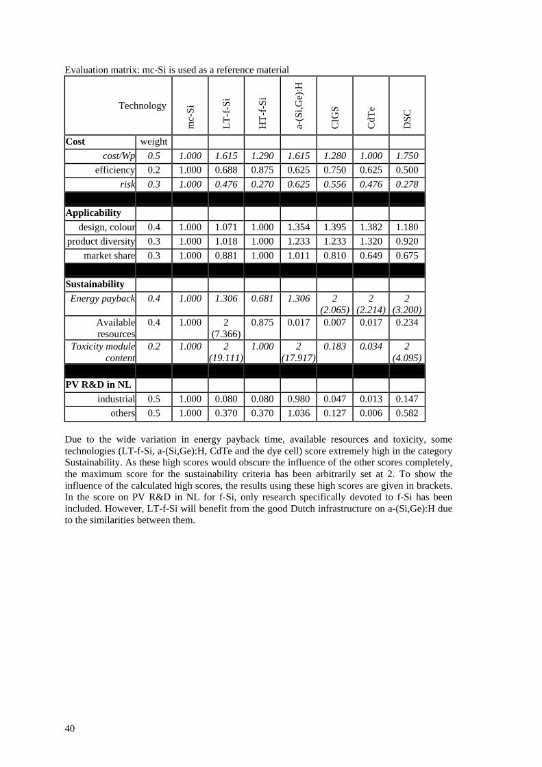
40
Evaluation matrix: mc-Si is used as a reference material
Technology
mc-
Si
LT
-f-S
i
HT
-f-S
i
a-(S
i,Ge)
:H
CIG
S
CdT
e
DSC
Cost weight
cost/Wp 0.5 1.000 1.615 1.290 1.615 1.280 1.000 1.750
efficiency 0.2 1.000 0.688 0.875 0.625 0.750 0.625 0.500
risk 0.3 1.000 0.476 0.270 0.625 0.556 0.476 0.278
Applicability
design, colour 0.4 1.000 1.071 1.000 1.354 1.395 1.382 1.180
product diversity 0.3 1.000 1.018 1.000 1.233 1.233 1.320 0.920
market share 0.3 1.000 0.881 1.000 1.011 0.810 0.649 0.675
Sustainability
Energy payback 0.4 1.000 1.306 0.681 1.306 2(2.065)
2(2.214)
2(3.200)
Availableresources
0.4 1.000 2(7.366)
0.875 0.017 0.007 0.017 0.234
Toxicity modulecontent
0.2 1.000 2(19.111)
1.000 2(17.917)
0.183 0.034 2(4.095)
PV R&D in NL
industrial 0.5 1.000 0.080 0.080 0.980 0.047 0.013 0.147
others 0.5 1.000 0.370 0.370 1.036 0.127 0.006 0.582
Due to the wide variation in energy payback time, available resources and toxicity, sometechnologies (LT-f-Si, a-(Si,Ge):H, CdTe and the dye cell) score extremely high in the categorySustainability. As these high scores would obscure the influence of the other scores completely,the maximum score for the sustainability criteria has been arbitrarily set at 2. To show theinfluence of the calculated high scores, the results using these high scores are given in brackets.In the score on PV R&D in NL for f-Si, only research specifically devoted to f-Si has beenincluded. However, LT-f-Si will benefit from the good Dutch infrastructure on a-(Si,Ge):H dueto the similarities between them.
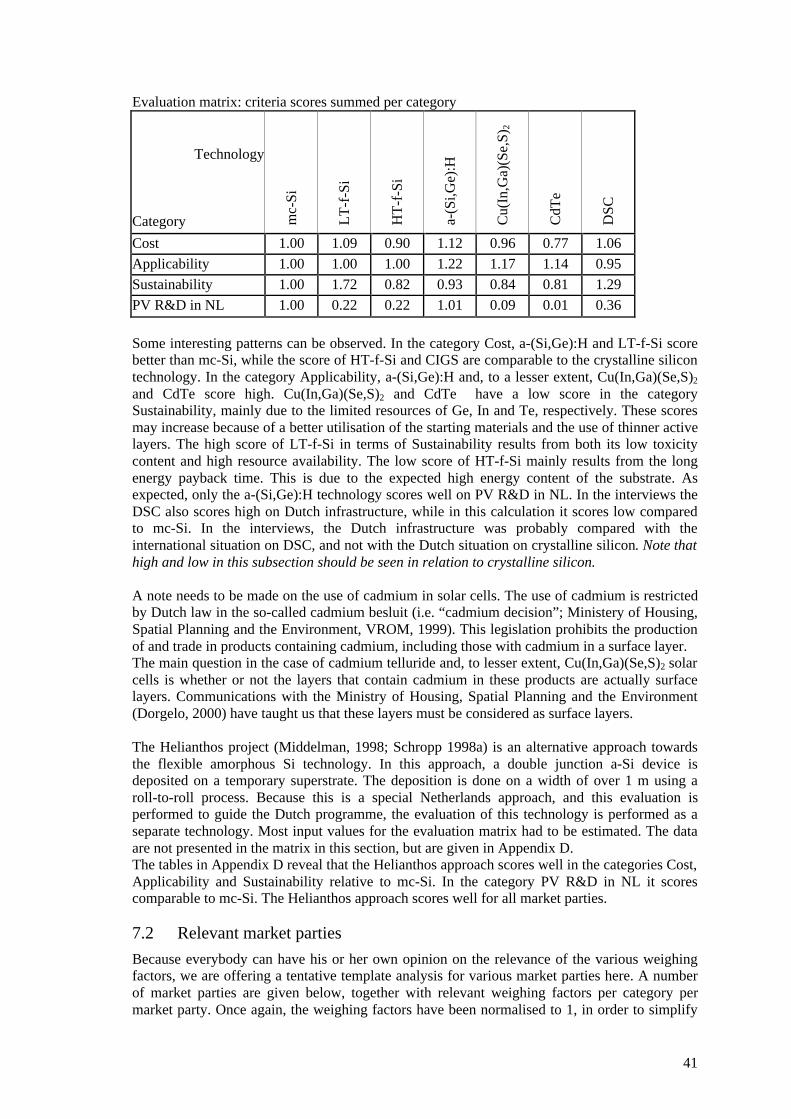
41
Evaluation matrix: criteria scores summed per category
Technology
Category mc-
Si
LT
-f-S
i
HT
-f-S
i
a-(S
i,Ge)
:H
Cu(
In,G
a)(S
e,S)
2
CdT
e
DSC
Cost 1.00 1.09 0.90 1.12 0.96 0.77 1.06
Applicability 1.00 1.00 1.00 1.22 1.17 1.14 0.95
Sustainability 1.00 1.72 0.82 0.93 0.84 0.81 1.29
PV R&D in NL 1.00 0.22 0.22 1.01 0.09 0.01 0.36
Some interesting patterns can be observed. In the category Cost, a-(Si,Ge):H and LT-f-Si scorebetter than mc-Si, while the score of HT-f-Si and CIGS are comparable to the crystalline silicontechnology. In the category Applicability, a-(Si,Ge):H and, to a lesser extent, Cu(In,Ga)(Se,S)2
and CdTe score high. Cu(In,Ga)(Se,S)2 and CdTe have a low score in the categorySustainability, mainly due to the limited resources of Ge, In and Te, respectively. These scoresmay increase because of a better utilisation of the starting materials and the use of thinner activelayers. The high score of LT-f-Si in terms of Sustainability results from both its low toxicitycontent and high resource availability. The low score of HT-f-Si mainly results from the longenergy payback time. This is due to the expected high energy content of the substrate. Asexpected, only the a-(Si,Ge):H technology scores well on PV R&D in NL. In the interviews theDSC also scores high on Dutch infrastructure, while in this calculation it scores low comparedto mc-Si. In the interviews, the Dutch infrastructure was probably compared with theinternational situation on DSC, and not with the Dutch situation on crystalline silicon. Note thathigh and low in this subsection should be seen in relation to crystalline silicon.
A note needs to be made on the use of cadmium in solar cells. The use of cadmium is restrictedby Dutch law in the so-called cadmium besluit (i.e. “cadmium decision”; Ministery of Housing,Spatial Planning and the Environment, VROM, 1999). This legislation prohibits the productionof and trade in products containing cadmium, including those with cadmium in a surface layer.The main question in the case of cadmium telluride and, to lesser extent, Cu(In,Ga)(Se,S)2 solarcells is whether or not the layers that contain cadmium in these products are actually surfacelayers. Communications with the Ministry of Housing, Spatial Planning and the Environment(Dorgelo, 2000) have taught us that these layers must be considered as surface layers.
The Helianthos project (Middelman, 1998; Schropp 1998a) is an alternative approach towardsthe flexible amorphous Si technology. In this approach, a double junction a-Si device isdeposited on a temporary superstrate. The deposition is done on a width of over 1 m using aroll-to-roll process. Because this is a special Netherlands approach, and this evaluation isperformed to guide the Dutch programme, the evaluation of this technology is performed as aseparate technology. Most input values for the evaluation matrix had to be estimated. The dataare not presented in the matrix in this section, but are given in Appendix D.The tables in Appendix D reveal that the Helianthos approach scores well in the categories Cost,Applicability and Sustainability relative to mc-Si. In the category PV R&D in NL it scorescomparable to mc-Si. The Helianthos approach scores well for all market parties.
7.2 Relevant market parties
Because everybody can have his or her own opinion on the relevance of the various weighingfactors, we are offering a tentative template analysis for various market parties here. A numberof market parties are given below, together with relevant weighing factors per category permarket party. Once again, the weighing factors have been normalised to 1, in order to simplify
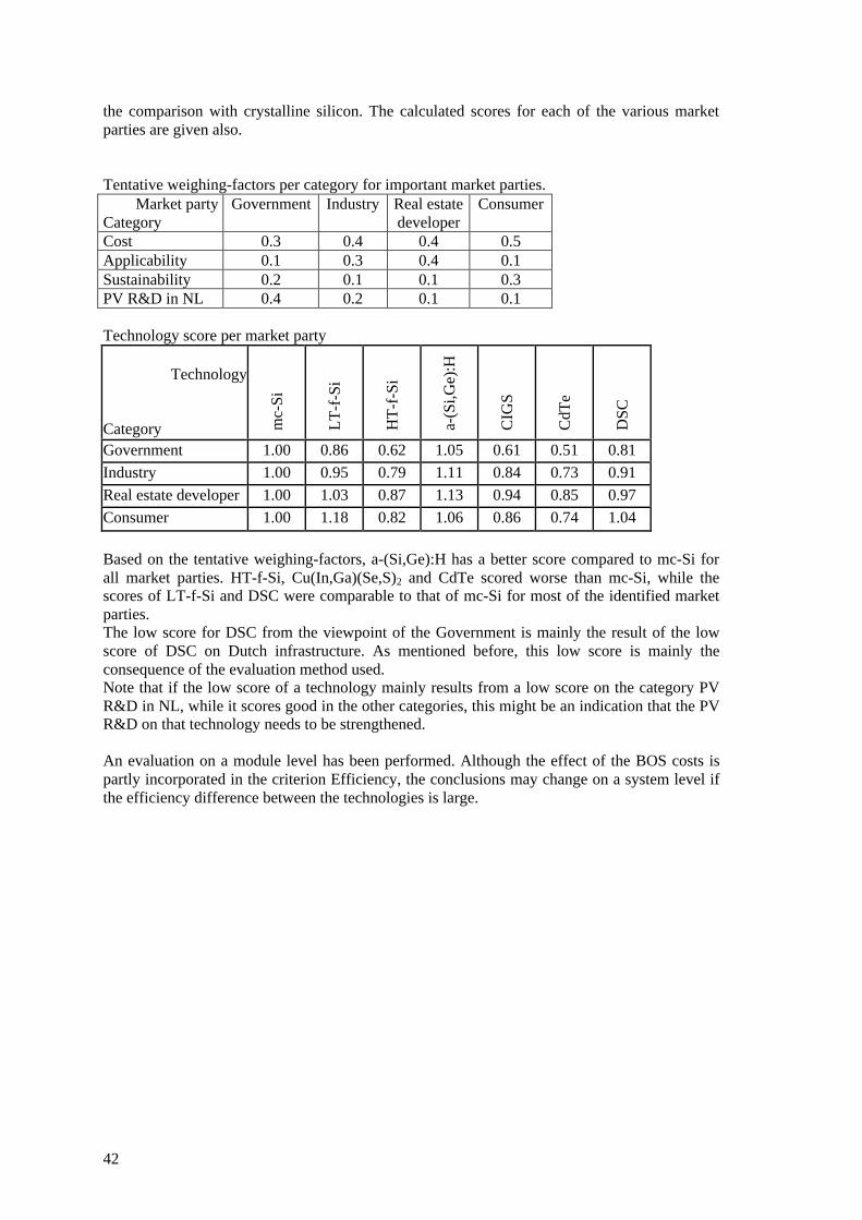
42
the comparison with crystalline silicon. The calculated scores for each of the various marketparties are given also.
Tentative weighing-factors per category for important market parties.Market party
CategoryGovernment Industry Real estate
developerConsumer
Cost 0.3 0.4 0.4 0.5Applicability 0.1 0.3 0.4 0.1Sustainability 0.2 0.1 0.1 0.3PV R&D in NL 0.4 0.2 0.1 0.1
Technology score per market party
Technology
Category mc-
Si
LT
-f-S
i
HT
-f-S
i
a-(S
i,Ge)
:H
CIG
S
CdT
e
DSC
Government 1.00 0.86 0.62 1.05 0.61 0.51 0.81
Industry 1.00 0.95 0.79 1.11 0.84 0.73 0.91
Real estate developer 1.00 1.03 0.87 1.13 0.94 0.85 0.97
Consumer 1.00 1.18 0.82 1.06 0.86 0.74 1.04
Based on the tentative weighing-factors, a-(Si,Ge):H has a better score compared to mc-Si forall market parties. HT-f-Si, Cu(In,Ga)(Se,S)2 and CdTe scored worse than mc-Si, while thescores of LT-f-Si and DSC were comparable to that of mc-Si for most of the identified marketparties.The low score for DSC from the viewpoint of the Government is mainly the result of the lowscore of DSC on Dutch infrastructure. As mentioned before, this low score is mainly theconsequence of the evaluation method used.Note that if the low score of a technology mainly results from a low score on the category PVR&D in NL, while it scores good in the other categories, this might be an indication that the PVR&D on that technology needs to be strengthened.
An evaluation on a module level has been performed. Although the effect of the BOS costs ispartly incorporated in the criterion Efficiency, the conclusions may change on a system level ifthe efficiency difference between the technologies is large.
43
8. CONCLUSION
In this evaluation a 5 years time frame is used. The, at present, most explored technologies arex-Si, a-Si, CIGS and CdTe. Therefore, a large amount of information is available for thesetechnologies. This provides a clear view on critical process and manufacturing steps, indicatedin the technology maps. However several technologies (f-Si, DSC, and organic solar cells) stillhave a long development period (> 5 years). Therefore, the uncertainty for these technologies ismuch larger (either in numerical value or in time frame). Despite this recognised uncertainty, a5 years time frame provides in our view the most workable and reliable technology profile. The5 years perspective used to evaluated the technologies is similar to the time indicationsmentioned by the interviewed experts in managing their research activities.
Interesting patterns can be observed in the evaluation matrix. In the Cost category a-(Si,Ge):Hand LT-f-Si score better than mc-Si, while HT-f-Si and CIGS score comparably with thecrystalline silicon technology. In the Applicability category, a-(Si,Ge):H and, to a lesser extentCu(In,Ga)(Se,S)2 and CdTe score high. These last two technologies score low in the categorySustainability, mainly due to the limited resources of Ge, In and Te, respectively. In the future,these scores may increase because of a better utilisation of the starting materials and the use ofthinner active layers. The high score of LT-f-Si in the Sustainability category results from bothits low toxicity content and high resource availability. The low score of HT-f-Si is mainly theresult of the long energy payback time. This is due to the expected high-energy content of thesubstrate. As expected, only the a-(Si,Ge):H technology scores well on PV R&D in NL. In theinterviews the DSC also scores high on Dutch infrastructure, while in this calculation it scoreslow compared to mc-Si. In the interviews, the Dutch infrastructure is compared with theinternational situation on DSC, rather than with the Dutch situation on crystalline silicon.Note that high and low in this paragraph means relative to crystalline silicon.
The exploration and optimisation of the optical and electrical solar cell properties are the presentR&D focus. Basic issues are the thorough understanding of the material deposition processesand characterisation results. Industrial activities are concentrated on high rate and low costmanufacturing processes. At present the industry is investing (world-wide) mainly in the x-Si,a-(Si,Ge):H, Cu(In,Ga)(Se,S)2 and CdTe technologies.
The interviews with experts indicate a positive belief in the x-Si and a-(Si,Ge):H technologieson the criteria Costs, Efficiency and Risk control. The technology mapping confirms thisexpectations by indicating a low-risk profile on the readiness of the dominant processtechnologies. In scaling up the Cu(In,Ga)(Se,S)2 and CdTe technologies, a major difficulty isthe control of active layer deposition over a large area. The critical risk involved on processingLT-f-Si is the deposition of the active layer. It is expected that a-(Si,Ge):H and LT-f-Si willmerge into one technology. The dye-sensitised and the organic solar cell are expected to becomeimportant in the long term. Much basic and applied research still has to be done on the electricalproperties of polymeric materials and the stability.
During the interviews, several experts mentioned that more co-operation between European /Benelux research groups and industry is important. The thin-film solar-cell development is aworld wide activity, and the competitors in the USA, Japan and Germany are strong (largebudget, big R&D institutes and much industry). The organic solar cell is still too unexplored toscore on the several criteria.
44
9. REFERENCES
Alsema, E.A.. Energy pay-back time and CO2 emissions of PV systems. In: Progress inphotovoltaics: research and applications. John Wiley & Sons, 2000.
Alsema, E.A.; Engelenburg, B.C.W.. Risiko’s en milieu-effecten van polykristallijne dunne-laag zonnecellen. Utrecht, Vakgroep Natuurwetenschap en samenlevening UniversiteitUtrecht, 1992.
Andersson, B.A.. Materials availability for large-scale thin-film photovoltaics. In: Progress inphotovoltaics: research and applications. John Wiley & Sons, 2000.
Antec, 2000; http://www.antec-gmbh.com
Bach U., Lupo D., Comte P., Moser J.E., Weissö F., Salbeck J., Spreitzer H., Grätzel M.; Solid-state dye-sensitized mesoporous TiO2 solar cells with high proton-to-electron conversionefficiencies; Nature, 395, 583-585, 1998
Bauhuis G.J., Schermer J.J., Mulder P., Haverkamp E.J., Voncken M.M.A.J. and Larsen P.K.;High rate weight induced epitaxial lift-off for high efficiency III/V film solar cells. 16th
European Photovoltaic Solar Energy Conference, 1-5 May 2000, Glasgow, UnitedKingdom.
Bergmann, R. B. (1999); Crystalline Si thin-film solar cells: a review, Applied Physics A.Solidsand Surfaces, 69, pp 187-194, 1999.
Bilyalov R.R., Solanski C.S., Poortmans J. and Nijs J. The Silicon Films for Solar Cells basedon Porous Silicon.16th European Photovoltaic Solar Energy Conference, 1-5 May 2000,Glasgow, United Kingdom.
Bonnet D., private communication 2000
Bonnet, D. and Meyers, P. (1998); Cadmium-telluride - material for thin film solar cells,Journal of Materials Research, 13(10), pp 2740-2753, 1998.
BP Solar. Multi-megawatt upscaling of silicon and thin film solar cell and modulemanufacturing – MUSIC FM. Sunbury on Thames, BP Solar, 1996.
Brabec C.J., Fromherz T., Padinger F., Sariciftci N.S., Janssen R.A.J., Hummelen J.C.;Interpenetrating networks of fullerenes and conjugated polymers for plastic photovoltaics;16th European Photovoltaic Solar Energy Conference, 1-5 May 2000, Glasgow, UnitedKingdom.
Bultman J.H., Weeber A.W., Brieko M.W., Hoornstra J., Burgers A.R., Dijkstra J.A., Tip A.C.,Schuurmans F.M.; Pin up module: a design for higher efficiency, easy modulemanufacturing and attractive appearance, presented at 16th EPSEC, Glasgow, 1-5 May2000.
Catchpole K.R., Weber K.J., Sproul A.B. and Blakers A.W. Characterisation of SiliconEpitaxial Layers for Solar Cell Applications. 16th European Photovoltaic Solar EnergyConference, 1-5 May 2000, Glasgow, United Kingdom
Caymax M.R., Leong W.Y., Low thermal budget chemical vapour deposition techniques for Siand SiGe, chapter 4 in Advance silicon & semiconducting silicon-alloy based materials &devices, Ed: Nijs, J.F.A., Institute of Physics Publishing, Bristol, 1994.
Christiaans M.P.T., Wienk M.M., Hal P.A.v., Kroon J.M., Janssen R.A.J.; Photoinducedelectron transfer from conjugated polymers onto TiO2; Synthet Metal 101, 265-266, 1999.
45
Degrave S., Burgelman M., Nollet P.; Electrical properties of copper indium disulphide(CuInS2) solar cells on copper substrates produced by the CISCuT-process; 16th EuropeanPhotovoltaic Solar Energy Conference, 1-5 May 2000, Glasgow, United Kingdom.
Dorgelo, letter no DGM/SVS/2000057847, 16 May 2000.
Durose K.; CdTe/CdS solar cell: materials factors; European Research ConferencePhotovoltaic Devices Thin Film Technology, 31 March – 5 April 2000, Teltow, Germany.
Eberspacher C., Fredric C., Pauls K. and Serra J.; Thin-film CIGS PV modules fabricated usingsimple, non-vacuum techniques. 16th European Photovoltaic Solar Energy Conference, 1-5May 2000, Glasgow, United Kingdom.
Eberspacher, C.; Fthenakis, V.M.; Moskowitz, P.D.. Environmental, health and safety issuesrelated to commercializing CuInSe2-based photovoltaics. New York, Brookhaven NationalLaboratory, 1996.
Eikelboom J.A., personal communication (1999)
Engelenburg, B.C.W. van; Alsema, E.A.. Environmental aspects and risks of amourphoussilicon solar cells. Utrecht, Department of Science, Technology and Society of Universityof Utrecht, 1993.
EPV, 2000; http://www.epv.net
Feldrapp K., Scholten D., Oelting D., Nagel H., Steinhof M., Auer R. and Brendel R. Thinmonocrystalline Si Solar Cells fabricated by the porous Si (PSi) Process using IonAssisted Deposition. 16th European Photovoltaic Solar Energy Conference, 1-5 May 2000,Glasgow, United Kingdom.
Ferro Electronic Materials. Division.Material Safety Data Sheet.
Frantzis, L.; Jones, E.. Opportunities for cost reduction in photovoltaic modules; presented at16th EPSEC, Glasgow, 1-5 May 2000
Glasgow, private communications at the 16th EPSEC, 1-5 May 2000.
Grätzel, M.. A new solar cell based on the principe of plant photosynthesis. Lausanne, Institutde chimie-physique, Ecole Polytechnique Fédérale, 1994.
Green M.A., Third generation photovoltaics: advanced structures capable of high efficiency atlow cost, presented at 16th EPSEC, Glasgow, 1-5 May 2000.
Groenendaal B., Lange T.J. de, Lako P., Roosmalen J.A.M. van, Tool C.J.J., Critical successfactors for the large-scale deployment of grid-connected photovoltaic systems, A surveyfocussing on the non-technical aspects, ECN-report, to be published, 2000.
Guha S., Yang, J., Banerje A., Hoffman K., Sugiyama S., Call J., Jones S.J., Deng X., DoehlerJ., Izu M., Ovshinsky H.C.; Triple junction amorphous silicon alloy PV manufacturingplant of 5 MW annual capacity; 26th IEEE Photovoltaic Specialists Conference, 29September – 3 October 1997, Anaheim, CA; pp. 607-610.
Güldner R., Penndorf J., Winkler M. and Tober O. Flexible, Polymer Encapsulated SolarModules - A new Concept for Cu-In-S Solar Devices Produced by the CISCuTTechnology. 16th European Photovoltaic Solar Energy Conference, 1-5 May 2000,Glasgow, United Kingdom.
Hagedorn, G.; Hellriegel, E.. Umweltrelevante Masseneinträge bei der Herstellungverschiedener Solarzelltypen: eine vergleichende Analyse konventioneller undausgewälter neuer Verfahren unter Berücksichtung der Einsatsstoffe und Prozeßkettensowie der Entsorgungs- und Recyclingmöglichkeiten: Teil 1: Konventionelle Verfahren.München, Forschungsstelle für Energiewirtshaft, 1992.
46
Hal P.A.van, Christiaans M.P.T., Wienk M.M., Kroon J.M., and Janssen R.A.J.; Photoinducedelectron transfer from conjugated polymers to TiO2; J.Phys.Chem.B 103, 4352-4359,1999.
Hamakawa Y.; Recent advances in solar photovoltaic activities in Japan and new energystrategy for 21st century; 16th European Photovoltaic Solar Energy Conference, 1-5 May2000, Glasgow, United Kingdom.
Hebling, C., Eyer, A., Faller, F. R., Hurrle, A., Lüdemann, R., Reber, S. and Wettling, W.(1998); The crystalline silicon thin-film solar cell. The high temperature approach,Festkörperprobleme, 38, pp 607-622, 1998.
Heijungs, R.; e.a.. Handleiding milieugerichte levenscyclusanalyse van producten. Leiden,Centrum voor Milieukunde, 1992.
Hinsch A., Kroon J.M., Späth M., Roosmalen J.A.M. van, Bakker N.J., Sommeling P., Burg N.van der, Kinderman R., Kern R., Ferber J., Schill C., Schubert M., Meyer A., Meyer T.,Uhlendorf I., Holzbock J., Niepmann R., Long-term stability of dye sensitized solar cellsfor large area power applications (LOTS-DSC), 16th European Photovoltaic Solar EnergyConference, 1-5 May 2000, Glasgow, United Kingdom.
Ichikawa Y., Yoshida T., Hama T., Sakai H., Harashima K.; Production technology foramorphous silicon based flexible solar cells; 11th International Photovoltaic Science andEngineering Conference, 20-24 September 1999, Sapporo, Japan, pp. 49-52.
Jacobs K., Penndorf J., Röser D., Tober O., Winkler M.; CISCuT – A non-vacuum roll to rolltechnique for the preparation of copper indium chalcogenide absorber layers on coppertape; 2nd World Photovoltaic Solar Energy Conference, 6-10 July 1998, Vienna, Austria;pp. 409-412.
Kampen B.J.M. van, Jansen W.C.H.C., Knelpunten bij de inpassing van fotovoltaïsche zonne-energie in de gebouwde omgeving, TNO-report 98-BBI-R0966, 1999.
Kapur, V.K.. Low cost manufacturing of PV modules through improved CIS technology.Presented at: World Photovoltaic Power ’97, San Diego 1999.
Karg F.H., Gay R.R.; Experience with manufacturing CIS products; European ResearchConference Photovoltaic Devices Thin Film Technology, 31 March – 5 April 2000,Teltow, Germany.
Kazmerski L.L., Rannels J.; The US PV programme; 16 th European Photovoltaic Solar EnergyConference, 1-5 May 2000, Glasgow, United Kingdom.
Kazmerski, L.L.; Photovoltaics R&D: A tour through the 21st century; 16th EuropeanPhotovoltaic Solar Energy Conference, 1-5 May 2000a, Glasgow, United Kingdom.
Kessler, F., Herz K., Powalla M., Baumgärtner K.-M., Schulz A.; Herrero; CIS thin-film solarcells on metal foils; 16th European Photovoltaic Solar Energy Conference, 1-5 May 2000,Glasgow, United Kingdom.
Klenk R., Luck I., Klaer J., Scheer R., Dobson P., Falz M., Janke N., Pérez-Rodríguez A.,Romano-Rodríguez, Terzini E.; SULFURCELL: Efficient thin film solar cells based onCuInS2; 16th European Photovoltaic Solar Energy Conference, 1-5 May 2000, Glasgow,United Kingdom.
KNMI (Royal Dutch Meteorological Institute). Test Reference Year De Bilt.
Korevaar B.A., Adriaenssens G.J., Smets A.H.M., Kessels W.M.M., Song H.-Z., SandenM.C.M. van de, Schram D.C.; High hole drift mobility in a-Si:H deposited at high growthrates for solar cell application; J. of Non Cryst. Sol., 266, 380-384, 2000.
Kraus M.M., Status of thin-film manufacturing technologies with respect to maturity forindustrial application, Fraunhofer Management GmbH, 1999.
47
Kubo W., Murakoshi K., Kitamura T., Wada Y., Hanabusa K., Shirai H., Yanagida S.;Fabrication of quasi-solid-state dye-sensitized TiO2 solar cells using low molecularweight gelators; Chemistry Letters, 1241-1242, 1998.
Linz, 2000; http://www.ipc.uni-liz.ac.at
Maycock, P.D.. Photovoltaic technology, performance, and cost 1995-2010. Warrenton, PVEnergy Systems, 2000.
Maycock, P.D.. The world photovoltaic market 1975-1998. Warrenton, PV Energy Systems,1999.
Meissner D., Rostalski J.; Highly efficient molecular organic solar cells; 16th EuropeanPhotovoltaic Solar Energy Conference, 1-5 May 2000, Glasgow, United Kingdom.
Middelman E., Andel E. van, Schropp R.E.I., Jonge-Meschaninova L.V. de, Peters P.M.G.M.,Severens R.J., Meiling H., Zeman M., Sanden M.C.M. van de, Kuijpers A., SpeeC.I.M.A., Jongerden G.J.; New temporary superstrate process for roll-to-roll productionof thin film solar cells; 2nd World Photovoltaic Solar Energy Conference, 6-10 July 1998,Vienna, Austria; pp. 816-819.
Mikoshiba S., Sumino H., Yonetsu M., Hayase S.; High efficiency photoelectrochemical cellwith novel polymer-gel-electrolytes; 16th European Photovoltaic Solar Energy Conference,1-5 May 2000, Glasgow, United Kingdom.
Ministerie van VROM [Dutch Ministry of Housing, Spatial Planning and the Environment].Cadmiumbesluit Wms 1999, The Hague, 1999.
Möller J.; Fischer Ch.-H., Siebentritt S.; Könenkamp R., Lux-Steiner M.Ch.; CuInS2 as anextremely thin absorber in an eta solar cell; 2nd World Photovoltaic Solar EnergyConference, 6-10 July 1998, Vienna, Austria; pp. 209-211.
Nath P., Vogeli C., Singh A., Slominsky L., Call J., Walters M., Guha S.; Amorphous siliconalloy based building integrated PV roofing elements; 2nd World Photovoltaic Solar EnergyConference, 6-10 July 1998, Vienna, Austria; pp. 2538-2541.
NCPV, U.S. Photovoltaics industry, PV technology roadmap workshop,Chicago, Il, 22-25 June1999.
Nijs, J. (2000); Visie op NOZ-PV zonnecelonderzoek, presented at the Dutch NOZ-PVconference, Bussum 17 February 2000.
Nijs, J. F., Szlufcik, J., Poortmans, J., Sivoththaman, S. and Mertens, R. P. (1999); Advancedmanufacturing concepts for crystalline silicon solar cells, IEEE Transactions on ElectronDevices, 46(10), pp 1948-1969, 1999.
Özsan M.E.; Large area electrodeposited CdTe solar cells; European Research ConferencePhotovoltaic Devices Thin Film Technology, 31 March – 5 April 2000, Teltow, Germany.
Petritsch K., Granström M., Arias A.C., Friend R.H., Lux A., Rozenberg G.G., Moratti S.C.,Holmes A.B., Andersson M.R.; Towards inexpensive solar cells; 2nd World PhotovoltaicSolar Energy Conference, 6-10 July 1998, Vienna, Austria; pp. 2411-2414.
Phylipsen, G.J.M.; Alsema, E.A.. Environmental life-cycle assessment of multicrystallinesilicon solar cell modules. Utrecht, Department of Science, Technology and SocietyUtrecht University, 1995.
Poortmans J., Diet A., Raeuber A., Survey of the European activities and progress in the fieldof CVD-grown crystalline Si thin-films for solar cells on low-cost insulating substrates,presented at 16th EPSEC, Glasgow, 1-5 May 2000.
Powalla M., Dimmler B.; CIS thin film photovoltaic modules; European Research ConferencePhotovoltaic Devices Thin Film Technology, 31 March – 5 April 2000, Teltow, Germany.
48
Powalla M., Dimmler B.; Manufacturing issues and strategies of CIGS solar modules massproduction; 16th European Photovoltaic Solar Energy Conference, 1-5 May 2000a,Glasgow, United Kingdom.
Rannels J.E.; Photovoltaics, Eneregy for the new millennium, The national 2000-2004Photovoltaics program plan; NREL, Golden Co, 2000
Reber, S. and Wettling, W. (1999); High-temperature processing of crystalline silicon thin-filmsolar cells, Applied Physics A.Solids and Surfaces, 69, pp 215-220, 1999.
Rinke T.J., Bergmann R.B. and Werner J.H. Efficient Thin Film Solar Cells by Transfer ofMono-crystalline Si Layers. 16th European Photovoltaic Solar Energy Conference, 1-5May 2000, Glasgow, United Kingdom
Romeo N.; The role of front and back contact in the preparation of high efficiency thin filmCdTe/CdS solar cells; European Research Conference Photovoltaic Devices Thin FilmTechnology, 31 March – 5 April 2000, Teltow, Germany.
Roosmalen J.A.M. van; Third generation solar cells; European Research ConferencePhotovoltaic Devices Thin Film Technology, 31 March – 5 April 2000, Teltow, Germany.
Roosmalen J.A.M., Thin-film solar cells, ECN report ECN-C--95-107, 1995.
Rudmann D., Haug F.-J., Krejci M., Zogg H., Tiwari A.N.; Development of flexibleCu(In,Ga)Se2 solar cells on polymers with lift-off processes; 16th European PhotovoltaicSolar Energy Conference, 1-5 May 2000, Glasgow, United Kingdom.
RUG, 2000; http://www.fwn.rug.nl/solar
Ruseler, C.H.. De LCA-methodiek als richtinggevend element in ontwikkelingstrajecten? : Casestudy naar organische zonnecellen. Petten, Energieonderzoek Centrum Nederland, 1999.
Salafsky J.S., Schropp R.E.I.; Solid state polymer-semiconductor nanocrystal photovoltaicdevices; 2nd World Photovoltaic Solar Energy Conference, 6-10 July 1998, Vienna,Austria; pp. 272-275.
Schock, H. W. and Noufi, R. (2000); CIGS-based solar cells for the next millenium, Progress inPhotovoltaics: Research and Applications, 8, pp 151-160, 2000.
Schön J.H., Kloc C., Batlogg B.; Doped pentacene for efficient photovoltaic devices; 16th
European Photovoltaic Solar Energy Conference, 1-5 May 2000a, Glasgow, UnitedKingdom.
Schön J.H., Kloc Ch., Bucher E., Batlogg B.; Efficient organic photovoltaic diodes based ondoped pentacene; Nature 403, 408-410, 2000.
Schropp R.E.I., Middelman E., Andel E. van, Meiling H., Werf C.H.M. van der, PetersP.M.G.M., Jonge-Meschaninova L.V. de, Winkeler J., Severens R.J., Zeman M., SandenM.C.M. van de, Kuipers A., Spee C.I.M.A., Jongerden G.J.; Novel superstrate process fortextured SnO2:F/p+-i-n+ amorphous silicon solar cells suitable for roll-to-roll deposition;2nd World Photovoltaic Solar Energy Conference, 6-10 July 1998a, Vienna, Austria; pp.820-822.
Schropp, R.E.I.; Zeman, M.. Amorphous and microcrystalline silicon solar cells. Dordrecht,Kluwer Academic Publishers, 1998.
Shah A., Meier J., Torres P., Kroll U., Fischer D., Beck N., Wyrsch N., Keppner H., Recentprogress on microcrystalline solar cells, Proc. 26th IEEE PVSEC, Anahamein CA, p 569,1997.
Sinke W.C., Nederlands zonnecelonderzoek: waar staan we?; presented at the Dutch NOZ-PVconference, Bussum 17 February 2000.
49
Steinberger, H. Health, safety and environmental risks from the operation of CdTe and CISthin-film modules. In: Progress in photovoltaics: research and applications. Chichester,John Wiley & Sons, 1998.
Tang C.W.; Two-layer organic photovoltaic cell; Applied Physics Letters 48, 183-183, 1986.
Tawada Y., Yamagishi H.; Mass-production of large size a-Si modules and future plan; 11th
International Photovoltaic Science and Engineering Conference, 20-24 September 1999,Sapporo, Japan, pp. 53-55.
Tennakone K., Kumara G.R.R.A., Kumarasinghe A.R., Wijayantha K.G.U., Sirimanne P.M.; Adye-sensitized nano-porous solid-state photovoltaic cell; Semiconductor Science andTechnology 10, 1689-1693, 1995.
Tiwari A.N., Krejci M., Haug F.-J. Zogg H.; Development of Cu(In,Ga)Se2 solar cells onpolymer with a record efficiency of 12.8%; ; 11th International Photovoltaic Science andEngineering Conference, 20-24 September 1999, Sapporo, Japan, p. 992.
Tool, C.J.J.; Roosmalen, J.A.M. van; Daey Ouwens, J .. CISZO: the potential of CIS solar cells .ECN-report . ECN-C--99-046, 1999.
Uhlendorf I.; Dye sensitized solar cells and modules, efficiency and upscaling; EuropeanResearch Conference Photovoltaic Devices Thin Film Technology, 31 March – 5 April2000, Teltow, Germany.
US Bureau of Mines. Mineral Commodity Summaries. Reston, US Geological Survey, 2000.Internet: http://www.minerals.usgs.gov/minerals/pubs/commodity
Vries J.G. de, Scholtens B.J.R., Maes I., Grätzel M., Winkel S., Burnside S., Wolf M., HinschA., Kroon J.M., Ahlse M., Tjerneld F., Ferrero G., Bruno E., Hagfeldt A., Bradbury C.,Carlsson P., Pettersson H., Verspeekrio C.M., and Enninga I.C.; Negative Ames-test of cis-di(Thiocyanato)-N,N '-bis(4,4 '- dicarboxy-2,2 '-bipyridine)Ru(II), the sensitizer dye of thenanocrystalline TiO2 solar cell; Solar Energy Materials and Solar Cells 60, 43-49, 2000.
WAU, 2000; http://www.spb.wau.nl/oc/research/orgsolcells/index.htm
Yang J., Banerjee A., Lord K., Guha S.; Correlation of component cells with high efficiencyamorphous silicon alloy triple-juntion solar cells and modules; 2nd World PhotovoltaicSolar Energy Conference, 6-10 July 1998, Vienna, Austria; pp. 387-390.
Yu G., Gao J., Hummelen J.C., Wudl F., Heeger A.J.; Polymer photovoltaic cells: enhancedefficiencies via a network of internal donor-acceptor heterojunctions; Science 270, 1789-1791, 1995.
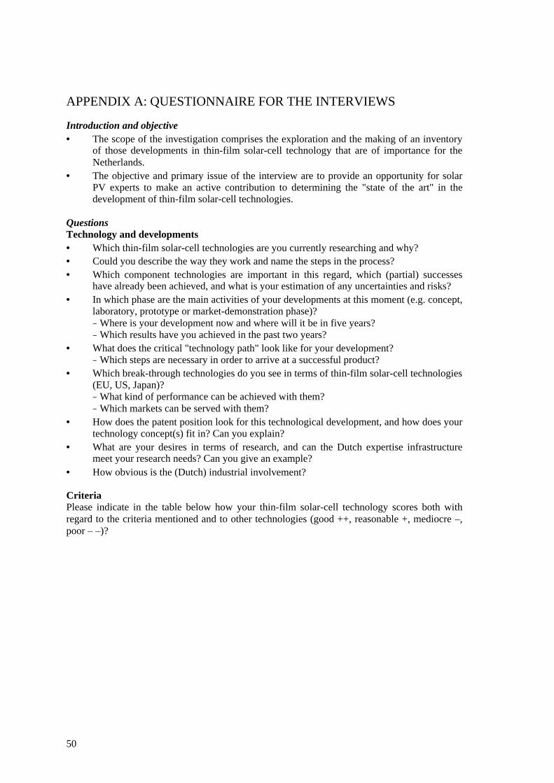
50
APPENDIX A: QUESTIONNAIRE FOR THE INTERVIEWS
Introduction and objective• The scope of the investigation comprises the exploration and the making of an inventory
of those developments in thin-film solar-cell technology that are of importance for theNetherlands.
• The objective and primary issue of the interview are to provide an opportunity for solarPV experts to make an active contribution to determining the "state of the art" in thedevelopment of thin-film solar-cell technologies.
QuestionsTechnology and developments• Which thin-film solar-cell technologies are you currently researching and why?• Could you describe the way they work and name the steps in the process?• Which component technologies are important in this regard, which (partial) successes
have already been achieved, and what is your estimation of any uncertainties and risks?• In which phase are the main activities of your developments at this moment (e.g. concept,
laboratory, prototype or market-demonstration phase)?− Where is your development now and where will it be in five years?− Which results have you achieved in the past two years?
• What does the critical "technology path" look like for your development?− Which steps are necessary in order to arrive at a successful product?
• Which break-through technologies do you see in terms of thin-film solar-cell technologies(EU, US, Japan)?− What kind of performance can be achieved with them?− Which markets can be served with them?
• How does the patent position look for this technological development, and how does yourtechnology concept(s) fit in? Can you explain?
• What are your desires in terms of research, and can the Dutch expertise infrastructuremeet your research needs? Can you give an example?
• How obvious is the (Dutch) industrial involvement?
CriteriaPlease indicate in the table below how your thin-film solar-cell technology scores both withregard to the criteria mentioned and to other technologies (good ++, reasonable +, mediocre –,poor – –)?
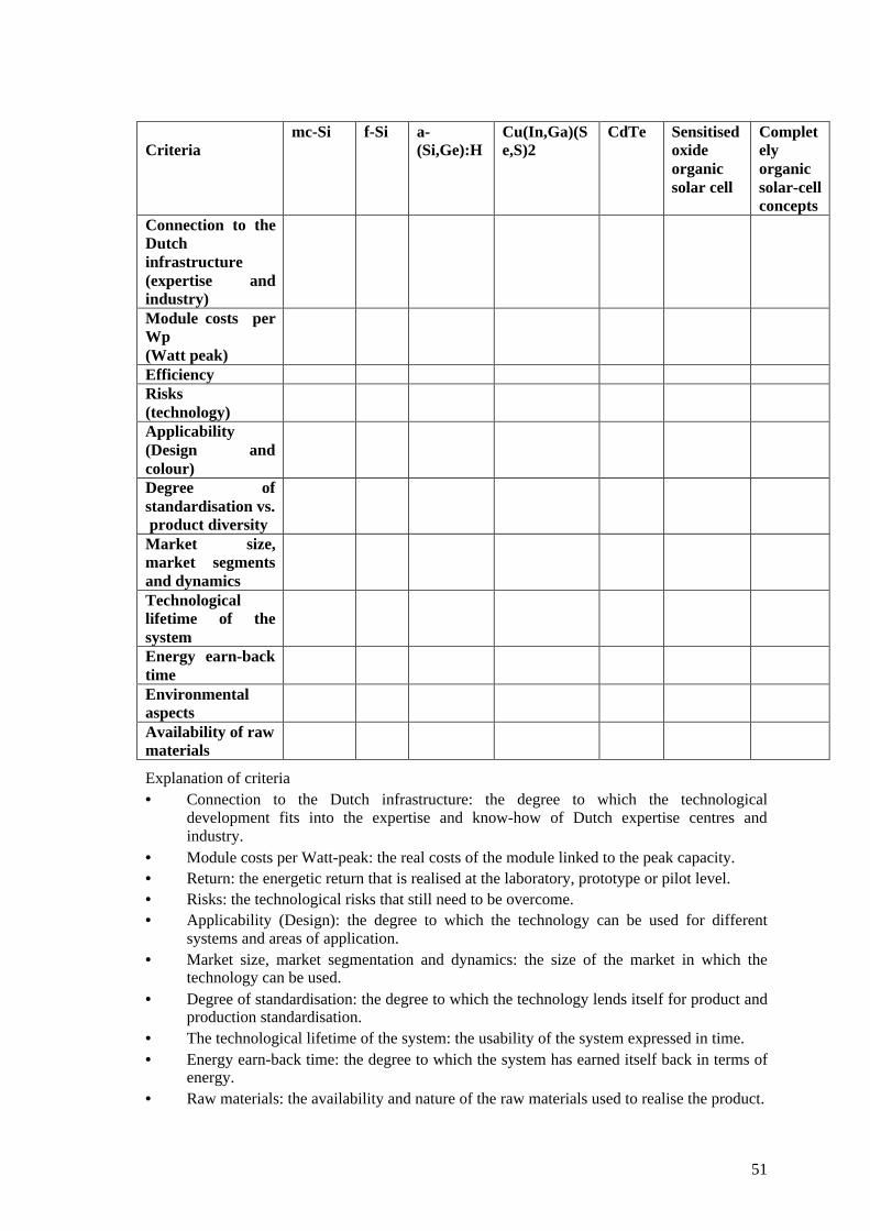
51
Criteriamc-Si f-Si a-
(Si,Ge):HCu(In,Ga)(Se,S)2
CdTe Sensitisedoxideorganicsolar cell
Completelyorganicsolar-cellconcepts
Connection to theDutchinfrastructure(expertise andindustry)Module costs perWp(Watt peak)EfficiencyRisks(technology)Applicability(Design andcolour)Degree ofstandardisation vs. product diversityMarket size,market segmentsand dynamicsTechnologicallifetime of thesystemEnergy earn-backtimeEnvironmentalaspectsAvailability of rawmaterials
Explanation of criteria• Connection to the Dutch infrastructure: the degree to which the technological
development fits into the expertise and know-how of Dutch expertise centres andindustry.
• Module costs per Watt-peak: the real costs of the module linked to the peak capacity.• Return: the energetic return that is realised at the laboratory, prototype or pilot level.• Risks: the technological risks that still need to be overcome.• Applicability (Design): the degree to which the technology can be used for different
systems and areas of application.• Market size, market segmentation and dynamics: the size of the market in which the
technology can be used.• Degree of standardisation: the degree to which the technology lends itself for product and
production standardisation.• The technological lifetime of the system: the usability of the system expressed in time.• Energy earn-back time: the degree to which the system has earned itself back in terms of
energy.• Raw materials: the availability and nature of the raw materials used to realise the product.
52
Can you briefly explain the reasons for your score for each of these criteria?
Management
• What is your vision and strategy in terms of the further elaboration of the technologicaldevelopments?
• On the basis of which indicators do you manage the developmental technologies?− Hours, budget, laboratory results, market expectations, etc.− Which indicators do you use?
• Do R&D developments take place in collaboration with other parties?− Which companies or research institutions are those?− How do you experience the collaboration with other parties?− Which success factors play a role in this?
• How are your developmental activities currently financed and which interests play a rolein this respect?− Concerned parties and roles− Access to market channels
General
• Do you have relevant research data or publications that could contribute to this survey(e.g. technological road-mapping, market analyses, solar-cell R&D programme memos,scenario planning, etc.)?
• Are there any other subjects that you feel should be mentioned?
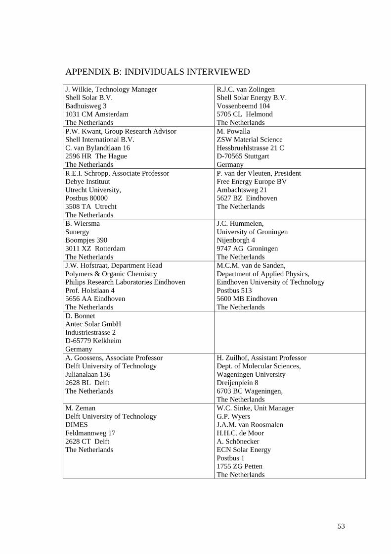
53
APPENDIX B: INDIVIDUALS INTERVIEWED
J. Wilkie, Technology ManagerShell Solar B.V.Badhuisweg 31031 CM AmsterdamThe Netherlands
R.J.C. van ZolingenShell Solar Energy B.V.Vossenbeemd 1045705 CL HelmondThe Netherlands
P.W. Kwant, Group Research AdvisorShell International B.V.C. van Bylandtlaan 162596 HR The HagueThe Netherlands
M. PowallaZSW Material ScienceHessbruehlstrasse 21 CD-70565 StuttgartGermany
R.E.I. Schropp, Associate ProfessorDebye InstituutUtrecht University,Postbus 800003508 TA UtrechtThe Netherlands
P. van der Vleuten, PresidentFree Energy Europe BVAmbachtsweg 215627 BZ EindhovenThe Netherlands
B. WiersmaSunergyBoompjes 3903011 XZ RotterdamThe Netherlands
J.C. Hummelen,University of GroningenNijenborgh 49747 AG GroningenThe Netherlands
J.W. Hofstraat, Department HeadPolymers & Organic ChemistryPhilips Research Laboratories EindhovenProf. Holstlaan 45656 AA EindhovenThe Netherlands
M.C.M. van de Sanden,Department of Applied Physics,Eindhoven University of TechnologyPostbus 5135600 MB EindhovenThe Netherlands
D. BonnetAntec Solar GmbHIndustriestrasse 2D-65779 KelkheimGermanyA. Goossens, Associate ProfessorDelft University of TechnologyJulianalaan 1362628 BL DelftThe Netherlands
H. Zuilhof, Assistant ProfessorDept. of Molecular Sciences,Wageningen UniversityDreijenplein 86703 BC Wageningen,The Netherlands
M. ZemanDelft University of TechnologyDIMESFeldmannweg 172628 CT DelftThe Netherlands
W.C. Sinke, Unit ManagerG.P. WyersJ.A.M. van RoosmalenH.H.C. de MoorA. SchöneckerECN Solar EnergyPostbus 11755 ZG PettenThe Netherlands
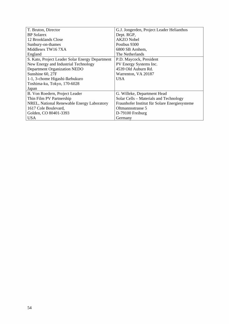
54
T. Bruton, DirectorBP Solarex12 Brooklands CloseSunbury-on-thamesMiddlesex TW16 7XAEngland
G.J. Jongerden, Project Leader HelianthosDept. RGP,AKZO NobelPostbus 93006800 SB Arnhem,The Netherlands
S. Kato, Project Leader Solar Energy DepartmentNew Energy and Industrial TechnologyDepartment Organization NEDOSunshine 60, 27F1-1, 3-chome Higashi-IkebukuroToshima-ku, Tokyo, 170-6028Japan
P.D. Maycock, PresidentPV Energy Systems Inc.4539 Old Auburn Rd.Warrenton, VA 20187USA
B. Von Roedern, Project LeaderThin Film PV PartnershipNREL, National Renewable Energy Laboratory1617 Cole Boulevard,Golden, CO 80401-3393USA
G. Willeke, Department HeadSolar Cells – Materials and TechnologyFraunhofer Institut für Solare EnergiesystemeOltmannsstrasse 5D-79100 FreiburgGermany
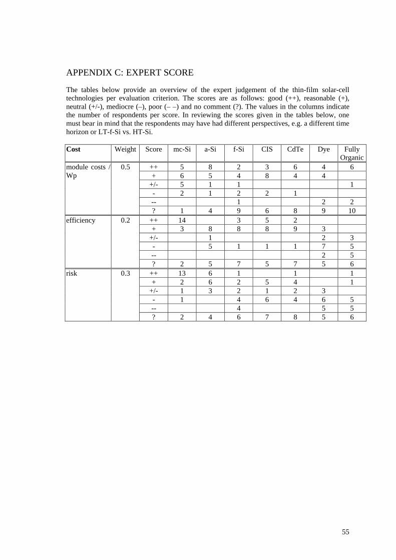
55
APPENDIX C: EXPERT SCORE
The tables below provide an overview of the expert judgement of the thin-film solar-celltechnologies per evaluation criterion. The scores are as follows: good (++), reasonable (+),neutral (+/-), mediocre (–), poor (– –) and no comment (?). The values in the columns indicatethe number of respondents per score. In reviewing the scores given in the tables below, onemust bear in mind that the respondents may have had different perspectives, e.g. a different timehorizon or LT-f-Si vs. HT-Si.
Cost Weight Score mc-Si a-Si f-Si CIS CdTe Dye FullyOrganic
++ 5 8 2 3 6 4 6+ 6 5 4 8 4 4
+/- 5 1 1 1- 2 1 2 2 1-- 1 2 2
module costs /Wp
0.5
? 1 4 9 6 8 9 10++ 14 3 5 2+ 3 8 8 8 9 3
+/- 1 2 3- 5 1 1 1 7 5-- 2 5
efficiency 0.2
? 2 5 7 5 7 5 6++ 13 6 1 1 1+ 2 6 2 5 4 1
+/- 1 3 2 1 2 3- 1 4 6 4 6 5-- 4 5 5
risk 0.3
? 2 4 6 7 8 5 6
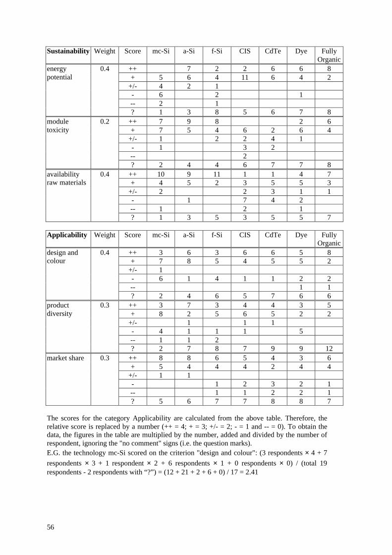
56
Sustainability Weight Score mc-Si a-Si f-Si CIS CdTe Dye FullyOrganic
++ 7 2 2 6 6 8+ 5 6 4 11 6 4 2
+/- 4 2 1- 6 2 1-- 2 1
energypotential
0.4
? 1 3 8 5 6 7 8++ 7 9 8 2 6+ 7 5 4 6 2 6 4
+/- 1 2 2 4 1- 1 3 2-- 2
moduletoxicity
0.2
? 2 4 4 6 7 7 8++ 10 9 11 1 1 4 7+ 4 5 2 3 5 5 3
+/- 2 2 3 1 1- 1 7 4 2-- 1 2 1
availabilityraw materials
0.4
? 1 3 5 3 5 5 7
Applicability Weight Score mc-Si a-Si f-Si CIS CdTe Dye FullyOrganic
++ 3 6 3 6 6 5 8+ 7 8 5 4 5 5 2
+/- 1- 6 1 4 1 1 2 2-- 1 1
design andcolour
0.4
? 2 4 6 5 7 6 6++ 3 7 3 4 4 3 5+ 8 2 5 6 5 2 2
+/- 1 1 1- 4 1 1 1 5-- 1 1 2
productdiversity
0.3
? 2 7 8 7 9 9 12++ 8 8 6 5 4 3 6+ 5 4 4 4 2 4 4
+/- 1 1- 1 2 3 2 1-- 1 1 2 2 1
market share 0.3
? 5 6 7 7 8 8 7
The scores for the category Applicability are calculated from the above table. Therefore, therelative score is replaced by a number (++ = 4; + = 3; +/- = 2; - = 1 and -- = 0). To obtain thedata, the figures in the table are multiplied by the number, added and divided by the number ofrespondent, ignoring the "no comment" signs (i.e. the question marks).E.G. the technology mc-Si scored on the criterion "design and colour": (3 respondents × 4 + 7
respondents × 3 + 1 respondent × 2 + 6 respondents × 1 + 0 respondents × 0) / (total 19respondents - 2 respondents with “?”) = (12 + 21 + 2 + 6 + 0) / 17 = 2.41
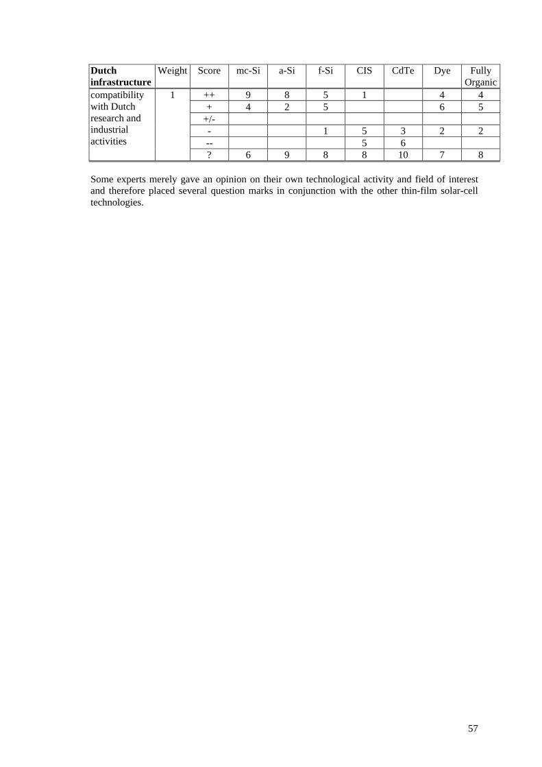
57
Dutchinfrastructure
Weight Score mc-Si a-Si f-Si CIS CdTe Dye FullyOrganic
++ 9 8 5 1 4 4+ 4 2 5 6 5
+/-- 1 5 3 2 2-- 5 6
compatibilitywith Dutchresearch andindustrialactivities
1
? 6 9 8 8 10 7 8
Some experts merely gave an opinion on their own technological activity and field of interestand therefore placed several question marks in conjunction with the other thin-film solar-celltechnologies.
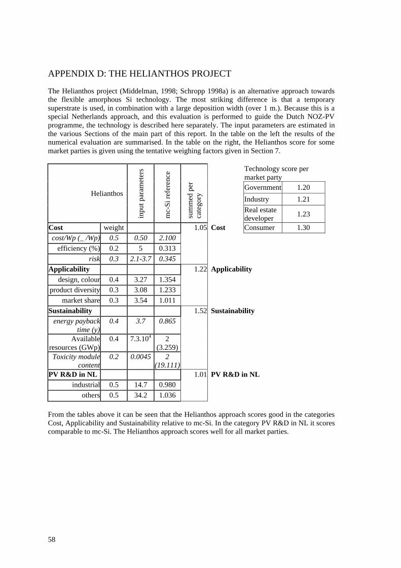
58
APPENDIX D: THE HELIANTHOS PROJECT
The Helianthos project (Middelman, 1998; Schropp 1998a) is an alternative approach towardsthe flexible amorphous Si technology. The most striking difference is that a temporarysuperstrate is used, in combination with a large deposition width (over 1 m.). Because this is aspecial Netherlands approach, and this evaluation is performed to guide the Dutch NOZ-PVprogramme, the technology is described here separately. The input parameters are estimated inthe various Sections of the main part of this report. In the table on the left the results of thenumerical evaluation are summarised. In the table on the right, the Helianthos score for somemarket parties is given using the tentative weighing factors given in Section 7.
Technology score permarket partyGovernment 1.20
Industry 1.21Helianthos
inpu
t par
amet
ers
mc-
Si r
efer
ence
sum
med
per
cate
gory
Real estatedeveloper
1.23
Cost weight 1.05 Cost Consumer 1.30cost/Wp (_/Wp) 0.5 0.50 2.100
efficiency (%) 0.2 5 0.313
risk 0.3 2.1-3.7 0.345Applicability 1.22 Applicability
design, colour 0.4 3.27 1.354product diversity 0.3 3.08 1.233
market share 0.3 3.54 1.011
Sustainability 1.52 Sustainabilityenergy payback
time (y)0.4 3.7 0.865
Availableresources (GWp)
0.4 7.3.104 2(3.259)
Toxicity modulecontent
0.2 0.0045 2(19.111)
PV R&D in NL 1.01 PV R&D in NLindustrial 0.5 14.7 0.980
others 0.5 34.2 1.036
From the tables above it can be seen that the Helianthos approach scores good in the categoriesCost, Applicability and Sustainability relative to mc-Si. In the category PV R&D in NL it scorescomparable to mc-Si. The Helianthos approach scores well for all market parties.